| website for students | vtu notes ...... | website for students | vtu notes | question papers |...
TRANSCRIPT
www.bookspar.com | Website for Students | VTU NOTES | QUESTION PAPERS | NEWS | RESULTS
www.bookspar.com | Website for Students | VTU NOTES | QUESTION PAPERS | NEWS | RESULTS
• Assembler: is a program that accepts an assembly language program as input and converts it into an object
module and prepares for loading the program into memory for execution. • Loader (linker) further converts the object module prepared by the assembler into executable form, by linking it
with other object modules and library modules. • The final executable map of the assembly language program is prepared by the loader at the time of loading into
the primary memory for actual execution. • The assembler prepares the relocation and linkages information (subroutine, ISR) for loader. • The operating system that actually has the control of the memory, which is to be allotted to the program for
execution, passes the memory address at which the program is to be loaded for execution and the map of the available memory to the loader.
• Based on this information and the information generated by the assembler, the loader generates an executable map of the program and further physically loads it into the memory and transfers control to for execution.
• Thus the basic task of an assembler is to generate the object module and prepare the loading and linking information.
Procedure for assembling a program • Assembling a program proceeds statement by statement sequentially. • The first phase of assembling is to analyze the program to be converted. This phase is called Pass1 defines and
records the symbols, pseudo operands and directives. It also analyses the segments used by the program types and labels and their memory requirements.
• The second phase looks for the addresses and data assigned to the labels. It also finds out codes of the instructions from the instruction machine, code database and the program data.
• It processes the pseudo operands and directives. • It is the task of the assembler designer to select the suitable strings for using them as directives, pseudo
operands or reserved words and decides syntax. Directives
• Also called as pseudo operations that control the assembly process. • They indicate how an operand or section of a program to be processed by the assembler. • They generate and store information in the memory.
Assembler Memory models • Each model defines the way that a program is stored in the memory system. • Tiny: data fits into one segment written in .COM format • Small: has two segments data and memory. • There are several other models too. Directive for string data in a memory segment
• DB define byte • DW define word • DD define double word • DQ define 10 bytes
Example Data1 DB 10H,11H,12H Data2 DW 1234H
• SEGMENT: statement to indicate the start of the program and its symbolic name. • Example
Name SEGMENT
www.bookspar.com | Website for Students | VTU NOTES | QUESTION PAPERS | NEWS | RESULTS
www.bookspar.com | Website for Students | VTU NOTES | QUESTION PAPERS | NEWS | RESULTS
Variable_name DB ……. Variable_name DW ……. Name ENDS Data SEGMENT Data1 DB ……. Data2 DW ……. Data ENDS Code SEGMENT START: MOV AX,BX … … … Code ENDS
Similarly the stack segment is also declared. • For small models
.DATA … … ENDS The ENDS directive indicates the end of the segment.
• Memory is reserved for use in the future by using a ? as an operand for DB DW or DD directive. The assembler sets aside a location and does not initialize it to any specific value (usually stores a zero). The DUP (duplicate) directive creates an array and stores a zero.
• Example Data1 DB 5 DUP(?) This reserves 5 bytes of memory for a array data1 and initializes each location with 05H
• ALIGN: memory array is stored in word boundaries. • Example
ALIGN 2 means storing from an even address
Address 0 XX Address 1 YY Address 2 XX
The data XX is aligned to the even address.
• ASSUME, EQU, ORG • ASSUME tells the assembler what names have been chosen for Code, Data Extra and Stack segments. Informs
the assembler that the register CS is to be initialized with the address allotted by the loader to the label CODE and DS is similarly initialized with the address of label DATA.
• Example ASSUME CS: Name of code segment ASSUME DS: Name of the data segment ASSUME CS: Code1, DS: Data1
• EQU: Equates a numeric, ASCII(American Standard Code for Information Interchange) or label to another label.
• Example Data SEGMENT
www.bookspar.com | Website for Students | VTU NOTES | QUESTION PAPERS | NEWS | RESULTS
www.bookspar.com | Website for Students | VTU NOTES | QUESTION PAPERS | NEWS | RESULTS
Num1 EQU 50H Num2 EQU 66H Data ENDS Numeric value 50H and 66H are assigned to Num1 and Num2
• ORG: Changes the starting offset address of the data in the data segment • Example
ORG 100H 100 data1 DB 10H it can be used for code too.
• PROC & ENDP: indicate the start and end of the procedure. They require a label to indicate the name of the procedure.
• NEAR: the procedure resides in the same code segment. (Local) • FAR: resides at any location in the memory. • Example
Add PROC NEAR ADD AX,BX MOV CX,AX RET Add ENDP PROC directive stores the contents of the register in the stack.
• EXTRN, PUBLIC informs the assembler that the names of procedures and labels declared after this directive have been already defined in some other assembly language modules.
• Example If you want to call a Factorial procedure of Module1 from Module2 it must be declared as PUBLIC in Module1.
• Example A sample for full segment definition Data SEGMENT Num1 DB 10H Num2 DB 20H Num3 EQU 30H Data ENDS ASSUME CS:Code,DS:Data Code SEGMENT START: MOV AX,Data MOV DS,AX MOV AX,Num1 MOV CX,Num2 ADD AX,CX Code ENDS
• Example
A sample for small model . MODEL SMALL .Data
www.bookspar.com | Website for Students | VTU NOTES | QUESTION PAPERS | NEWS | RESULTS
www.bookspar.com | Website for Students | VTU NOTES | QUESTION PAPERS | NEWS | RESULTS
Num1 DB 10H Num2 DB 20H Num3 EQU 30H .Code HERE: MOV AX,@Data MOV DS,AX MOV AX,Num1 MOV CX,Num2 ADD AX,CX
QUESTIONS
1: What is a directive? 2: Describe the purpose of DB DW and DQ directive? 3: What is the purpose of .386 directive? 4: What does START indicate? --------------------------------------------------------------------------------------------------------------------------------------------
www.bookspar.com | Website for Students | VTU NOTES | QUESTION PAPERS | NEWS | RESULTS
www.bookspar.com | Website for Students | VTU NOTES | QUESTION PAPERS | NEWS | RESULTS
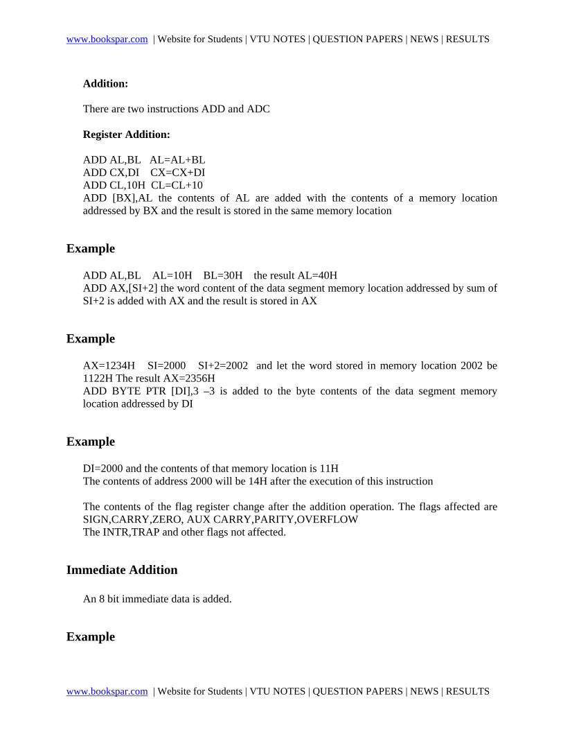
Addition: There are two instructions ADD and ADC Register Addition: ADD AL,BL AL=AL+BL ADD CX,DI CX=CX+DI ADD CL,10H CL=CL+10 ADD [BX],AL the contents of AL are added with the contents of a memory location addressed by BX and the result is stored in the same memory location
Example
ADD AL,BL AL=10H BL=30H the result AL=40H ADD AX,[SI+2] the word content of the data segment memory location addressed by sum of SI+2 is added with AX and the result is stored in AX
Example
AX=1234H SI=2000 SI+2=2002 and let the word stored in memory location 2002 be 1122H The result AX=2356H ADD BYTE PTR [DI],3 –3 is added to the byte contents of the data segment memory location addressed by DI
Example
DI=2000 and the contents of that memory location is 11H The contents of address 2000 will be 14H after the execution of this instruction The contents of the flag register change after the addition operation. The flags affected are SIGN,CARRY,ZERO, AUX CARRY,PARITY,OVERFLOW The INTR,TRAP and other flags not affected.
Immediate Addition An 8 bit immediate data is added.
Example
www.bookspar.com | Website for Students | VTU NOTES | QUESTION PAPERS | NEWS | RESULTS
www.bookspar.com | Website for Students | VTU NOTES | QUESTION PAPERS | NEWS | RESULTS
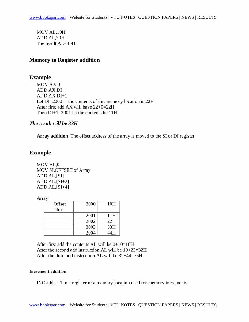
MOV AL,10H ADD AL,30H The result AL=40H
Memory to Register addition
Example MOV AX,0 ADD AX,DI ADD AX,DI+1 Let DI=2000 the contents of this memory location is 22H After first add AX will have 22+0=22H Then DI+1=2001 let the contents be 11H
The result will be 33H Array addition The offset address of the array is moved to the SI or DI register
Example
MOV AL,0 MOV SI,OFFSET of Array ADD AL,[SI] ADD AL,[SI+2] ADD AL,[SI+4]
Array
Offset addr
2000 10H
2001 11H 2002 22H 2003 33H 2004 44H
After first add the contents AL will be 0+10=10H After the second add instruction AL will be 10+22=32H After the third add instruction AL will be 32+44=76H
Increment addition
INC adds a 1 to a register or a memory location used for memory increments
www.bookspar.com | Website for Students | VTU NOTES | QUESTION PAPERS | NEWS | RESULTS
www.bookspar.com | Website for Students | VTU NOTES | QUESTION PAPERS | NEWS | RESULTS
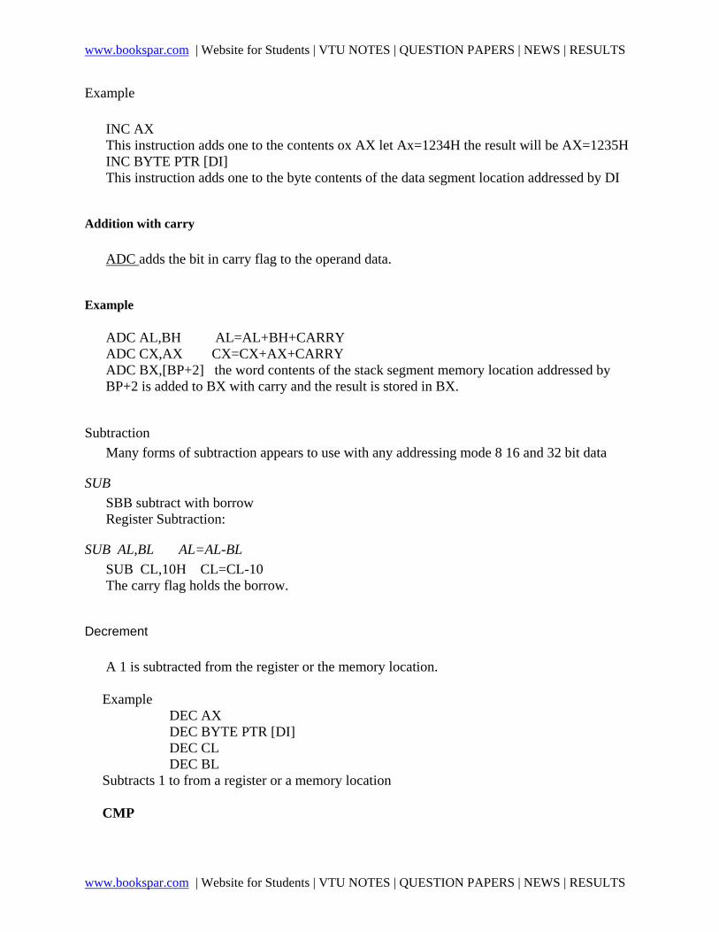
Example INC AX This instruction adds one to the contents ox AX let Ax=1234H the result will be AX=1235H INC BYTE PTR [DI] This instruction adds one to the byte contents of the data segment location addressed by DI
Addition with carry ADC adds the bit in carry flag to the operand data.
Example
ADC AL,BH AL=AL+BH+CARRY ADC CX,AX CX=CX+AX+CARRY ADC BX,[BP+2] the word contents of the stack segment memory location addressed by BP+2 is added to BX with carry and the result is stored in BX.
Subtraction Many forms of subtraction appears to use with any addressing mode 8 16 and 32 bit data
SUB SBB subtract with borrow Register Subtraction:
SUB AL,BL AL=AL-BL SUB CL,10H CL=CL-10 The carry flag holds the borrow.
Decrement A 1 is subtracted from the register or the memory location.
Example DEC AX DEC BYTE PTR [DI] DEC CL DEC BL Subtracts 1 to from a register or a memory location
CMP
www.bookspar.com | Website for Students | VTU NOTES | QUESTION PAPERS | NEWS | RESULTS
www.bookspar.com | Website for Students | VTU NOTES | QUESTION PAPERS | NEWS | RESULTS
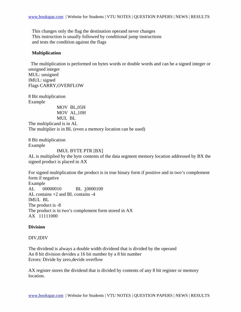
This changes only the flag the destination operand never changes This instruction is usually followed by conditional jump instructions and tests the condition against the flags Multiplication The multiplication is performed on bytes words or double words and can be a signed integer or unsigned integer MUL: unsigned IMUL: signed Flags CARRY,OVERFLOW 8 Bit multiplication Example MOV BL,05H MOV AL,10H MUL BL The multiplicand is in AL The multiplier is in BL (even a memory location can be used) 8 Bit multiplication Example IMUL BYTE PTR [BX] AL is multiplied by the byte contents of the data segment memory location addressed by BX the signed product is placed in AX For signed multiplication the product is in true binary form if positive and in two’s complement form if negative Example AL 00000010 BL 10000100 AL contains +2 and BL contains -4 IMUL BL The product is -8 The product is in two’s complement form stored in AX AX 11111000 Division DIV,IDIV The dividend is always a double width dividend that is divided by the operand An 8 bit division devides a 16 bit number by a 8 bit number Errors: Divide by zero,devide overflow AX register stores the dividend that is divided by contents of any 8 bit register or memory location.
www.bookspar.com | Website for Students | VTU NOTES | QUESTION PAPERS | NEWS | RESULTS
www.bookspar.com | Website for Students | VTU NOTES | QUESTION PAPERS | NEWS | RESULTS
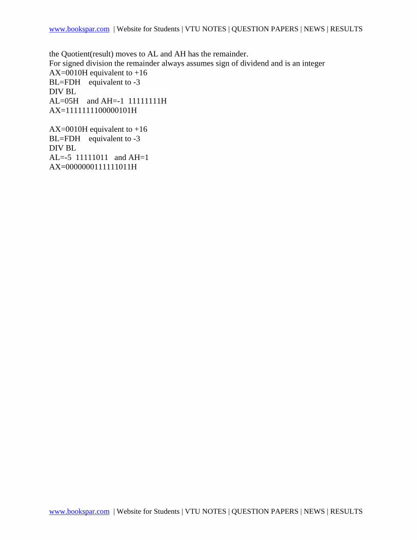
the Quotient(result) moves to AL and AH has the remainder. For signed division the remainder always assumes sign of dividend and is an integer AX=0010H equivalent to +16 BL=FDH equivalent to -3 DIV BL AL=05H and AH=-1 11111111H AX=1111111100000101H AX=0010H equivalent to +16 BL=FDH equivalent to -3 DIV BL AL=-5 11111011 and AH=1 AX=0000000111111011H
www.bookspar.com | Website for Students | VTU NOTES | QUESTION PAPERS | NEWS | RESULTS
www.bookspar.com | Website for Students | VTU NOTES | QUESTION PAPERS | NEWS | RESULTS
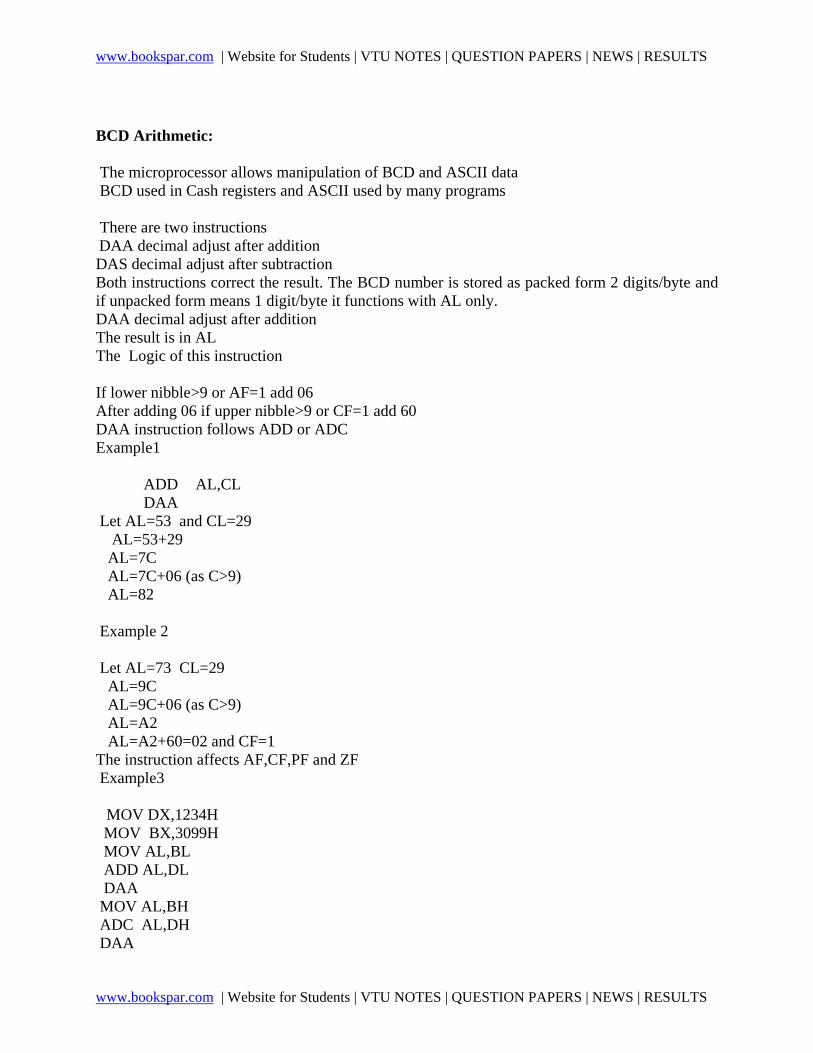
BCD Arithmetic: The microprocessor allows manipulation of BCD and ASCII data BCD used in Cash registers and ASCII used by many programs There are two instructions DAA decimal adjust after addition DAS decimal adjust after subtraction Both instructions correct the result. The BCD number is stored as packed form 2 digits/byte and if unpacked form means 1 digit/byte it functions with AL only. DAA decimal adjust after addition The result is in AL The Logic of this instruction If lower nibble>9 or AF=1 add 06 After adding 06 if upper nibble>9 or CF=1 add 60 DAA instruction follows ADD or ADC Example1 ADD AL,CL DAA Let AL=53 and CL=29 AL=53+29 AL=7C AL=7C+06 (as C>9) AL=82 Example 2 Let AL=73 CL=29 AL=9C AL=9C+06 (as C>9) AL=A2 AL=A2+60=02 and CF=1 The instruction affects AF,CF,PF and ZF Example3 MOV DX,1234H MOV BX,3099H MOV AL,BL ADD AL,DL DAA MOV AL,BH ADC AL,DH DAA
www.bookspar.com | Website for Students | VTU NOTES | QUESTION PAPERS | NEWS | RESULTS
www.bookspar.com | Website for Students | VTU NOTES | QUESTION PAPERS | NEWS | RESULTS
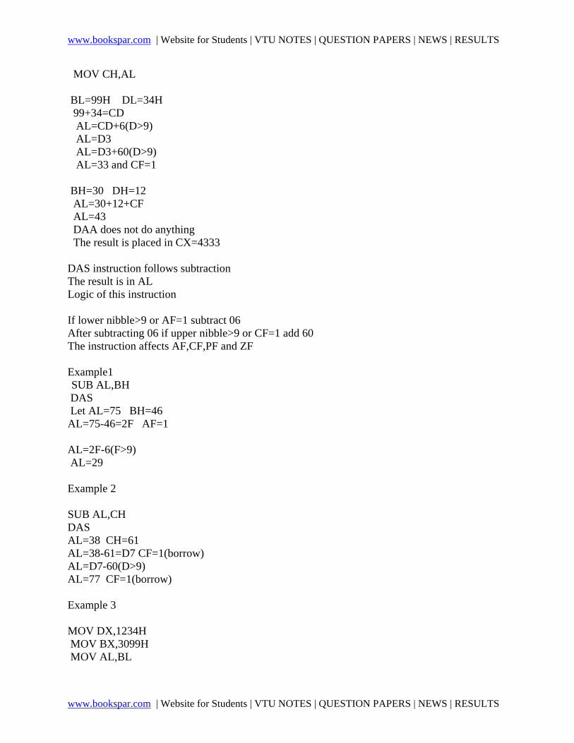
MOV CH,AL BL=99H DL=34H 99+34=CD AL=CD+6(D>9) AL=D3 AL=D3+60(D>9) AL=33 and CF=1 BH=30 DH=12 AL=30+12+CF AL=43 DAA does not do anything The result is placed in CX=4333 DAS instruction follows subtraction The result is in AL Logic of this instruction If lower nibble>9 or AF=1 subtract 06 After subtracting 06 if upper nibble>9 or CF=1 add 60 The instruction affects AF,CF,PF and ZF Example1 SUB AL,BH DAS Let AL=75 BH=46 AL=75-46=2F AF=1 AL=2F-6(F>9) AL=29 Example 2 SUB AL,CH DAS AL=38 CH=61 AL=38-61=D7 CF=1(borrow) AL=D7-60(D>9) AL=77 CF=1(borrow) Example 3 MOV DX,1234H MOV BX,3099H MOV AL,BL
www.bookspar.com | Website for Students | VTU NOTES | QUESTION PAPERS | NEWS | RESULTS
www.bookspar.com | Website for Students | VTU NOTES | QUESTION PAPERS | NEWS | RESULTS
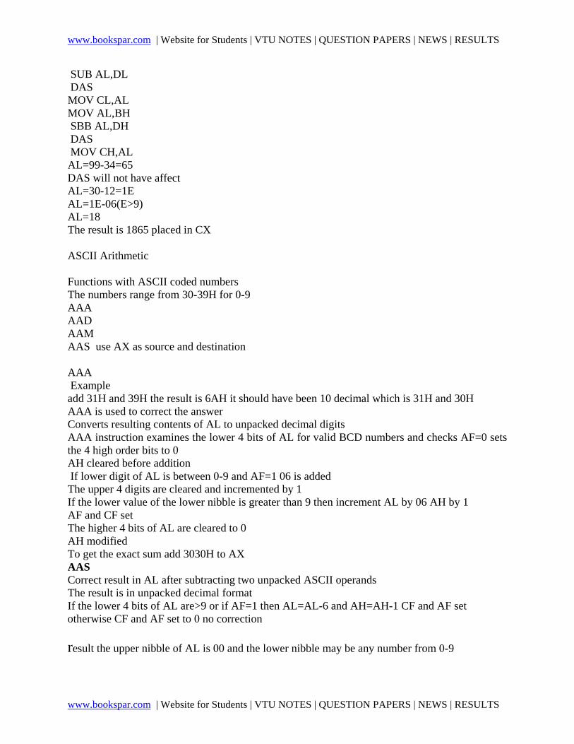
SUB AL,DL DAS MOV CL,AL MOV AL,BH SBB AL,DH DAS MOV CH,AL AL=99-34=65 DAS will not have affect AL=30-12=1E AL=1E-06(E>9) AL=18 The result is 1865 placed in CX ASCII Arithmetic Functions with ASCII coded numbers The numbers range from 30-39H for 0-9 AAA AAD AAM AAS use AX as source and destination AAA Example add 31H and 39H the result is 6AH it should have been 10 decimal which is 31H and 30H AAA is used to correct the answer Converts resulting contents of AL to unpacked decimal digits AAA instruction examines the lower 4 bits of AL for valid BCD numbers and checks AF=0 sets the 4 high order bits to 0 AH cleared before addition If lower digit of AL is between 0-9 and AF=1 06 is added The upper 4 digits are cleared and incremented by 1 If the lower value of the lower nibble is greater than 9 then increment AL by 06 AH by 1 AF and CF set The higher 4 bits of AL are cleared to 0 AH modified To get the exact sum add 3030H to AX AAS Correct result in AL after subtracting two unpacked ASCII operands The result is in unpacked decimal format If the lower 4 bits of AL are>9 or if AF=1 then AL=AL-6 and AH=AH-1 CF and AF set otherwise CF and AF set to 0 no correction result the upper nibble of AL is 00 and the lower nibble may be any number from 0-9
www.bookspar.com | Website for Students | VTU NOTES | QUESTION PAPERS | NEWS | RESULTS
www.bookspar.com | Website for Students | VTU NOTES | QUESTION PAPERS | NEWS | RESULTS
AAM Follows multiplication instruction after multiplying two unpacked BCD numbers Converts the product available in AL into unpacked BCD Lower byte of result is in AL and upper in AH Example let the product is 5D in AL D>9 so add 6 =13H LSD of 13H is lower unpacked byte Increment AH, AH=5+1=6 upper unpacked byte After execution AH=06 and AL=03 MOV AL,5 MOV CL,5 MUL CL AAM Accomplishes conversion by dividing AX by 10 Benefit of AAM –converts from binary to unpacked BCD use of AAM for conversion XOR DX,DX MOV CX,100 DIV CX AAM ADD AX,3030H XCHG AX,DX AAM ADD AX,3030H AAD Appears before division requires AX to contain two digit unpacked BCD number(not ASCII) before executing After adjusting AX with AAD it is divided by an unpacked BCD number to generate a single digit result in AL with remainder in AH Example .MODEL .CODE .STARTUP MOV AL,48H MOV AH,0 AAM ADD AX,3030H MOV DL,AH MOV AH,2 PUSH AX INT 21H POP AX MOV DL,AL

www.bookspar.com | Website for Students | VTU NOTES | QUESTION PAPERS | NEWS | RESULTS
www.bookspar.com | Website for Students | VTU NOTES | QUESTION PAPERS | NEWS | RESULTS
INT 21H .EXIT END Logic instructions AND OR Exclusive OR NOT TEST The above instructions perform bitwise operation and the src and destination could be register or memory location. Their function is same as logic opeartions
www.bookspar.com | Website for Students | VTU NOTES | QUESTION PAPERS | NEWS | RESULTS
www.bookspar.com | Website for Students | VTU NOTES | QUESTION PAPERS | NEWS | RESULTS
Shift instructions They manipulate binary numbers Used to control I/O Devices. Shift operation moves the number either to left or right within memory location or a register. There are four instructions.There are two types of shift (1) arithmetic and (2) logical. The shift left operation is equivalent to multiply operation and shift right is divide operation. The data is shifted to left or right only by one position. Shift left operation Logical left: The contents of the register or memory location are shifted left by one position the MSB bit moves to Carry flag bit and a zero is added to the LSB position Example SHL AX,1 AX=0000 1111 0000 1111 and Carry=1 After the execution of the instruction AX=0001 1110 0001 1110 and Carry =0 Example MOV CL,3 SHL DX,CL The contents of the DX register are shifted left by three postions Arithmetical Left: It is same as logical left shift. Logical right: The contents of the register or memory location are shifted right by one position the LSB bit moves to Carry flag bit and a zero is added to the MSB position Example SHR AX,1 AX=0000 1111 0000 1111 and Carry=0 Result AX=0000 0111 1000 0111 and carry=1 Arithmetic right: The contents of the register or memory location are shifted right by one position the LSB bit moves to Carry flag bit and the sign bit is copied through the MSB position Example SAL AX,1 AX=1000 0000 0000 1111 and carry=0 Result AX=1100 0000 0000 0111 and carry=1
www.bookspar.com | Website for Students | VTU NOTES | QUESTION PAPERS | NEWS | RESULTS
www.bookspar.com | Website for Students | VTU NOTES | QUESTION PAPERS | NEWS | RESULTS
Example SAR SI,3 SI= 1010 1100 1010 0101 C=0 After first shift SI= 1101 0110 0101 0010 C=1 second shift SI=1110 1011 0010 1001 C=0 third shift SI= 1111 0101 1001 0100 C=1 All condition flags are affected Rotation instructions There are four rotate instructions. Rotate left: The contents of the memory location or the register are rotated left by the no of positions indicated in the instruction through the carry or without the carry. ROL BL,4 Let BL=0001 0110 C=0 After first rotate C= 0 BL= 0010 1100 After second rotate C=0 BL= 0101 1000 After third rotate C=0 BL= 1011 0000 After fourth rotate C=1 BL= 0110 0000 Rotate right The contents of the memory location or the register are rotated right by the no of positions indicated in the instruction through the carry or without the carry. String instructions REP it is a prefix used with instruction REPE/REPZ REPNE/REPNZ These are used with CMPS and SCAS instructions These instructions are used in the program as prefix. CMPS Compare string byte or string word Only Flags affected Zero flag set if strings match otherwise reset DS:SI and ES:DI are used to point to the two strings
www.bookspar.com | Website for Students | VTU NOTES | QUESTION PAPERS | NEWS | RESULTS
www.bookspar.com | Website for Students | VTU NOTES | QUESTION PAPERS | NEWS | RESULTS
SCAS Scans the string of bytes or words for an operand byte or word specified in register AL or AX When match found the ZF=1 otherwise it is reset LODS Load string byte or string word Loads the AL/AX register by the contents of a string pointed by DS:SI No flag affected STOS Stores contents of AL/AX register to a location in a string pointed by ES:DI No flag affected
www.bookspar.com | Website for Students | VTU NOTES | QUESTION PAPERS | NEWS | RESULTS
www.bookspar.com | Website for Students | VTU NOTES | QUESTION PAPERS | NEWS | RESULTS
A bus is used to communicate between components in a computer system. They are typically specialized, with (for instance) a memory bus having different characteristics from an IO bus. Communications used in networks are different again.
An important distinction to be drawn early is that between a bus and a point-to-point network. A bus has a single wire, or connection of wires with multiple sources and destinations. A point-to-point network has some sort of interconnection scheme between sources and destinations in which the nodes are endpoints. In general a bus is cheaper and slower than other network topologies; there is a shift in progress in some areas from busses to point-to-point networks; this is most noticeable in high-speed ethernet and in AMD's multiprocessor system ``busses.''
Bus operations should be thought of in terms of transactions. A bus transaction is an operation on the bus; for instance, a memory read, or an interrupt service, or an IO write. A bus transaction is initiated by a bus master who requests that some operation take place; a slave will respond to the transaction appropriately. Different busses support different sets of transactions
Bus Components Busses typically have several components in common. In general, dedicated groups of wires are used for the different components (but see multiplexing, below).
1. Data: this is the whole purpose of the bus - to transmit data. Ordinarily, when you talk about the ``width'' of a bus (8-bit bus, 32-bit bus, etc), you're talking about how many wires are used for data.
2. Address: this is how the components on the bus recognize that data on the bus is intended for them. Ordinarily, whenever a bus transaction takes place, an address is put on the bus... recipient can tell who it's for. Memory and IO busses don't normally put a source address on; that's either implicit in the transaction or irrelevant. Networks, on the other hand, usually do.
3. Control: these wires contain a variety of information about the transaction, for instance what type of transaction it is (read, write, interrupt request, etc). Most parallel busses may also have a global clock, which would be a control line as well. A serial bus can't very well do that, so the clock has to be carried with the data somehow.
4. Power and Ground: the bus has to have a ground wire, so the different components have a common voltage reference (they'll normally have lots of ground wires, for electrical immunity!). Also, all the cards in the bus need to get power from somewhere, so the bus itself is a convenient place to distribute it.
PCI Bus The Peripheral Component Interconnect (PCI) bus is the standard I/O bus on recent computers in general, and PCs in particular. It was developed by Intel in 1993 to replace the various busses which had been in use on both PCs and Macintoshes.
www.bookspar.com | Website for Students | VTU NOTES | QUESTION PAPERS | NEWS | RESULTS
www.bookspar.com | Website for Students | VTU NOTES | QUESTION PAPERS | NEWS | RESULTS
It is a 32-bit, 33MHz bus with multiplexed address and data, and very nice capabilities for autoconfiguration ("Plug and Play"). It also supports both old, 5 volt devices and newer, 3.3 volt devices.
Just as a brief note, it was developed by Intel in 1993 to replace the various busses which had been in use on both PCs and Macintoshes. To Intel's credit, it is a remarkably architecture-neutral bus. A very brief description would be that it is a 32-bit, 33MHz bus with multiplexed address and data, and very nice capabilities for autoconfiguration ("Plug and Play"). It also supports both old, 5 volt devices and newer, 3.3 volt devices.
There are many extensions to PCI. Best known is that it has simply been extended to 64 bits and 66 MHz. In addition, there is a variant called PC-104+, which is a 32-bit PCI bus in a highly shock and vibration resistant packaging. PCI-X is a backward-compatible extension to PCI, with PCI-X itself running at 266MHz and PCI-X 2.0 at 533 MHz. This latter also defines a 16 bit interface for space-constrained applications, and a new bus mastering protocol (PCI SIG likes to call this peer-to-peer) that looks a lot like messaging.
All transfers on the PCI bus are "burst" transfers. What this means is that once a device obtains the bus to perform a transfer, it is able to hang on to the bus indefinitely, and keep sending more data every bus cycle (there's actually a time in the bus controller which will take control back after some configurable time period, to keep transfers from being too long. The longer the tranfers are the better the throughput, but this can cause unacceptable delays for other devices).
Configuration Space
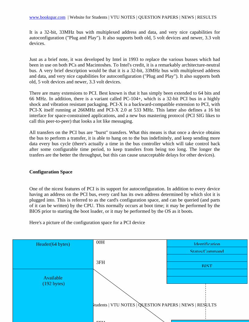
One of the nicest features of PCI is its support for autoconfiguration. In addition to every device having an address on the PCI bus, every card has its own address determined by which slot it is plugged into. This is referred to as the card's configuration space, and can be queried (and parts of it can be written) by the CPU. This normally occurs at boot time; it may be performed by the BIOS prior to starting the boot loader, or it may be performed by the OS as it boots.
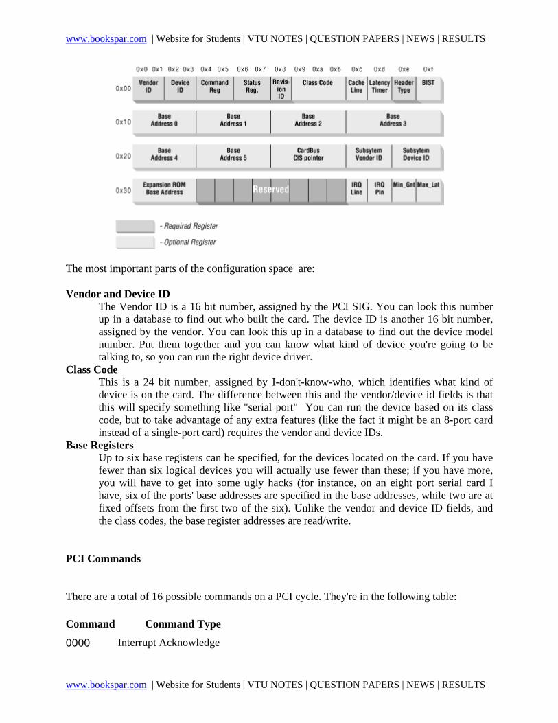
Here's a picture of the configuration space for a PCI device
Header(64 bytes)
Available (192 bytes)
00H
3FH
FFH
Identification Status/Command
BIST
www.bookspar.com | Website for Students | VTU NOTES | QUESTION PAPERS | NEWS | RESULTS
www.bookspar.com | Website for Students | VTU NOTES | QUESTION PAPERS | NEWS | RESULTS
The most important parts of the configuration space are:
Vendor and Device ID The Vendor ID is a 16 bit number, assigned by the PCI SIG. You can look this number up in a database to find out who built the card. The device ID is another 16 bit number, assigned by the vendor. You can look this up in a database to find out the device model number. Put them together and you can know what kind of device you're going to be talking to, so you can run the right device driver.
Class Code This is a 24 bit number, assigned by I-don't-know-who, which identifies what kind of device is on the card. The difference between this and the vendor/device id fields is that this will specify something like "serial port" You can run the device based on its class code, but to take advantage of any extra features (like the fact it might be an 8-port card instead of a single-port card) requires the vendor and device IDs.
Base Registers Up to six base registers can be specified, for the devices located on the card. If you have fewer than six logical devices you will actually use fewer than these; if you have more, you will have to get into some ugly hacks (for instance, on an eight port serial card I have, six of the ports' base addresses are specified in the base addresses, while two are at fixed offsets from the first two of the six). Unlike the vendor and device ID fields, and the class codes, the base register addresses are read/write.
PCI Commands
There are a total of 16 possible commands on a PCI cycle. They're in the following table:
Command Command Type
0000 Interrupt Acknowledge
www.bookspar.com | Website for Students | VTU NOTES | QUESTION PAPERS | NEWS | RESULTS
www.bookspar.com | Website for Students | VTU NOTES | QUESTION PAPERS | NEWS | RESULTS
0001 Special Cycle
0010 I/O Read
0011 I/O Write
0100 reserved
0101 reserved
0110 Memory Read
0111 Memory Write
1000 reserved
1001 reserved
1010 Configuration Read
1011 Configuration Write
1100 Multiple Memory Read
1101 Dual Address Cycle
1110 Memory-Read Line
1111 Memory Write and Invalidate
Here are some notes on the different transfer types
Interrupt Acknowledge (0000) The interrupt controller automatically recognizes and reacts to the INTA (interrupt acknowledge) command. In the data phase, it transfers the interrupt vector to the AD lines.
Special Cycle (0001) AD15-AD0
0x0000 Processor Shutdown
0x0001 Processor Halt
0x0002 x86 Specific Code
0x0003 to 0xFFFF Reserved I/O Read (0010) and I/O Write (0011)
Input/Output device read or write operation. The AD lines contain a byte address (AD0 and AD1 must be decoded). PCI I/O ports may be 8 or 16 bits. PCI allows 32 bits of address space. On IBM compatible machines, the Intel CPU is limited to 16 bits of I/O
www.bookspar.com | Website for Students | VTU NOTES | QUESTION PAPERS | NEWS | RESULTS
www.bookspar.com | Website for Students | VTU NOTES | QUESTION PAPERS | NEWS | RESULTS
space, which is further limited by some ISA cards that may also be installed in the machine (many ISA cards only decode the lower 10 bits of address space, and thus mirror themselves throughout the 16 bit I/O space). This limit assumes that the machine supports ISA or EISA slots in addition to PCI slots. The PCI configuration space may also be accessed through I/O ports 0x0CF8 (Address) and 0x0CFC (Data). The address port must be written first.
Memory Read (0110) and Memory Write (0111) A read or write to the system memory space. The AD lines contain a doubleword address. AD0 and AD1 do not need to be decoded. The Byte Enable lines (C/BE) indicate which bytes are valid.
Configuration Read (1010) and Configuration Write (1011) A read or write to the PCI device configuration space, which is 256 bytes in length. It is accessed in doubleword units. AD0 and AD1 contain 0, AD2-7 contain the doubleword address, AD8-10 are used for selecting the addressed unit a the malfunction unit, and the remaining AD lines are not used.
Multiple Memory Read (1100) This is an extension of the memory read bus cycle. It is used to read large blocks of memory without caching, which is beneficial for long sequential memory accesses.
Dual Address Cycle (1101) Two address cycles are necessary when a 64 bit address is used, but only a 32 bit physical address exists. The least significant portion of the address is placed on the AD lines first, followed by the most significant 32 bits. The second address cycle also contains the command for the type of transfer (I/O, Memory, etc). The PCI bus supports a 64 bit I/O address space, although this is not available on Intel based PCs due to limitations of the CPU.
Memory-Read Line (1110) This cycle is used to read in more than two 32 bit data blocks, typically up to the end of a cache line. It is more effecient than normal memory read bursts for a long series of sequential memory accesses.
Memory Write and Invalidate (1111) This indicates that a minimum of one cache line is to be transferred. This allows main memory to be updated, saving a cache write-back cycle.
Interrupt Handling PCI uses four pins, called INTA-INTD, for interrupt requests. When an interrupt is required, the proper pin is asserted. A card which only has a single interrupt will normally use INTA In the modern systems BIOS exists which support PCI bus ------------------------------------------------------------------------------------------------------------------

www.bookspar.com | Website for Students | VTU NOTES | QUESTION PAPERS | NEWS | RESULTS
www.bookspar.com | Website for Students | VTU NOTES | QUESTION PAPERS | NEWS | RESULTS
Port details The parallel port LPT1 is normally at I/O port addresses 378H, 379H and 37AH
The secondary port(if present) is located at 278H, 279H and 27AH The parallel printer interface is located on the rear of the PC LPT stands for Line printer The printer interface gives access to eight lines that can be programmed to receive or send data The Centronics interface implemented by the parallel port uses two connecters One is 25 pin D type on the back of the PC The other one is 36 pin on the back of the Printer The parallel port can work as both transmitter and as well as receiver Other than printers CD ROMs can also be interfaced through parallel port.
Universal Serial Bus (USB) allows the addition of a new device to a PC by plugging it into the back of the machine or daisy-chaining it from another device on the bus. The device is immediately available for use (no rebooting required) and often does not need a device driver to be installed (depending on the operating system being used.
USB 1.1 allows communication speeds of 12 Megabits per second (or 1.5 Megabytes per second). The enhanced USB 2.0 will use the same cables, connectors, and software interfaces and will be backward compatible with older devices. USB 2.0 carries data at 360 to 480 Mbps (60 MBps). All cables use four wires; the distance between two devices can be up to five meters.
A big advantage of USB devices, apart from their much greater speed, is that USB devices configure themselves automatically: gone are the days when you had to fiddle with IRQ settings, DMA channels, and I/O addresses to make a gadget work. Another benefit is that because USB devices do not require IRQ settings, DMA channels, or I/O settings, COM and LPT ports currently occupying an IRQ can be freed up, making more IRQ interrupts available for other uses.
Another advantage of USB is that it is a standard port and can support just about any type of device, including keyboards, mice, serial peripherals (e.g. modems), printers, audio input/output, joysticks, digital cameras, scanners, external hard disks and CD burners. Soon, the collection of space-consuming and costly dedicated ports for keyboards, printers, mice, modems etc will disappear and replaced by USB. USB can be built into most chipsets for about $1. The other advantage is that you can mix and match devices as much as you like. In the old days, if you had a parallel port scanner and a printer, they had to share the single printer port (and neither of them would work properly for long.)
If you have several USB devices, it is best to use a USB hub. This is a little box that splits a single USB port into 4 or more ports
www.bookspar.com | Website for Students | VTU NOTES | QUESTION PAPERS | NEWS | RESULTS
www.bookspar.com | Website for Students | VTU NOTES | QUESTION PAPERS | NEWS | RESULTS
USB uses a four-wire cable interface. Two of the wires are used in a differential mode for both transmitting and receiving data, and the remaining two wires are power and ground. The source of the power to a USB device can come from the host, a hub, or the device can be "self powered." There are two different connector types on each end of a USB cable. One of these connectors is for upstream communications, and the other for downstream. Each cable length is limited to about 5 meters. USB has four types of communication transfer modes:
• control, • interrupt, • bulk, and • isochronous.
Control mode is initiated by the host. In this mode, every data transfer must send data in both directions, but only in one direction at a time. The control mode is used mainly for initialization of devices, but it can also be used to transfer small amounts of data. In interrupt mode, interrupts do not occur in the usual sense. As in control mode, the host has to initiate the transfer of data. Interrupt mode works by the host querying devices to see if they need
To be serviced
Bulk mode and isochronous mode complement each other in a sense. Bulk mode is used when data accuracy is of prime importance, but the rate of data transfer is not guaranteed. An example of this would be disk drive storage. Isochronous mode sacrifices data accuracy in favor of guaranteed timing of data delivery. An example of this would be USB audio speakers. These four modes will be discussed in more detail below.
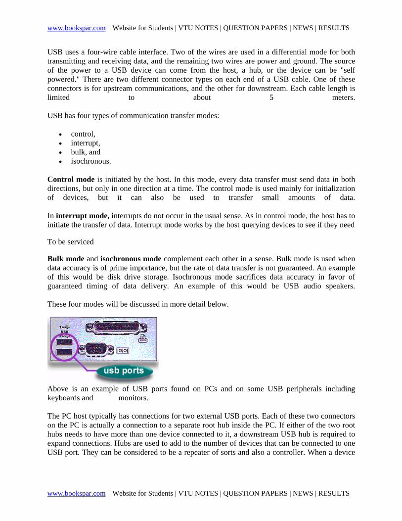
Above is an example of USB ports found on PCs and on some USB peripherals including keyboards and monitors. The PC host typically has connections for two external USB ports. Each of these two connectors on the PC is actually a connection to a separate root hub inside the PC. If either of the two root hubs needs to have more than one device connected to it, a downstream USB hub is required to expand connections. Hubs are used to add to the number of devices that can be connected to one USB port. They can be considered to be a repeater of sorts and also a controller. When a device
www.bookspar.com | Website for Students | VTU NOTES | QUESTION PAPERS | NEWS | RESULTS
www.bookspar.com | Website for Students | VTU NOTES | QUESTION PAPERS | NEWS | RESULTS
is connected downstream of a hub, the hub does the connect detection of the new device and notifies the host.
Hubs can be inside the device itself -- for example, in a keyboard that may have an additional two downstream USB connectors for additional devices. A hub can have a combination of high and low speed devices connected to it, up to a maximum of four additional hubs downstream from itself. A hub's upstream port to the PC must be high speed. The hub acts as a traffic cop, handling communication to downstream devices as either high or low speed. A hub can ignore a downstream device that is not behaving properly. Hubs can be either self-powered or receive power from the USB bus. USB 1.x hubs support both low and high-speed data transfers. There are several hardware requirements for devices that are placed on the USB bus. Five volts is the nominal supply voltage on the bus. A device that requires 100mA or less can be powered from the host or any hub, provided that the total available power hasn't already been exhausted by other devices. A device on the bus can draw up to 500mA from it. However, not all USB hosts (especially a battery powered PC) or bus-powered hubs will allow a device to draw more than 100mA from the bus. For this reason, a USB device that draws more than 100mA should, in most cases, be self-powered . A device tells the host how much current is required for its operation. Self-powered devices usually get their power from a separate power supply or batteries. A battery-powered device plugged into the bus can get its power from the bus if it meets the tests above, and it can then switch back over to battery power when it is disconnected from the bus or when the host is shut down. When a device is in suspend mode, it cannot draw any more than 500uA from the bus if it is bus-powered. Also, if a device has not seen any activity on its bus in 3 mS, it needs to go into suspend mode. A host can initiate a resume command to a device that is in suspend mode. A device can also issue a remote wakeup to an inactive host to make it active. All devices have endpoints, which are memory buffers. An endpoint can be as simple as an addressable single register, or it can be a block of memory that is used to store incoming and/or outgoing data. There may be multiple endpoints inside a device. Each device has at least one endpoint -- "endpoint 0"-- which is used as a control endpoint. It must be able to both send and receive data, but can only communicate in one direction at a time. Typically, when a device receives data such as an Out or Setup command from the host, this data is stored in the endpoint and the device's microprocessor is interrupted and works on this data. When a device receives an In command that is addressed to it from the host, data for the host that is stored in the endpoint is sent to the host. The host is considered to be the master in most all cases. One exception is when a device issues a remote wakeup to the host as discussed above. There are time limits for both the host and device to respond to each other. For example, if the host requests data from a device using an In command, the device must send the data back to the host within 500mS, in some cases. Depending on the transaction type, the host and/or the device may respond to data received with an acknowledgement. Data transfer involves quite a bit of error-checking and handshaking. The different types of data packets sent and received use different ways to verify correct data transfer. A logical connection link needs to be set up between the host and a device before a transaction can occur. This connection is referred to as a Pipe. It is set up as soon as possible after a host has recognized a device as being connected. When the host responds to a connect signal from the device, one of the parameters that is sent to the host is the device's required data transfer type and speed. The host can refuse to establish a Pipe if the host does not have enough bandwidth to support the device's request or if its power requirements cannot be met. The device at its
www.bookspar.com | Website for Students | VTU NOTES | QUESTION PAPERS | NEWS | RESULTS
www.bookspar.com | Website for Students | VTU NOTES | QUESTION PAPERS | NEWS | RESULTS
discretion can lower its requested data rate and try again until the host accepts it and initiates a Pipe. When a device is connected, it also sends to the host descriptor information on the types of endpoints in the device, the type of data transfer it uses, size of data packets, endpoint addresses within the device, and if used, the time required between data transfers. The following describes a typical data flow for a device when it is initially plugged into a host's bus while the host is active. Remember here that the host has an internal USB hub, and additional hubs may be connected downstream from the host's hub.
1. The host recognizes that a device has been attached to one of its USB hubs. It realizes this by a simple resistive divider that is connected to the differential data pair of wires in the USB bus. These resistors are inside the USB hubs and devices.
2. The host sends a Get_Port_Status request to the hub to find out more about what has been plugged in. It could be another hub, a device connected directly to the host hub, or a device that has been plugged into one of the downstream hubs.
3. After receiving a response from the hub, the host issues a Set_Port_Feature command in which the hub issues a reset over the data pair but only to the newly connected device on the USB bus.
4. The host then checks to see if the device has come out of the reset state by issuing a Get_Port_Status command to the hub. After reset, the device is in the Default state and can only draw a maximum of 100mA. In Default state, the device can communicate with the host through Endpoint 0.
5. The hub now detects the device's speed by using the resistive dividers that are attached to the USB bus. The hub sends the speed of this device back to the host.
6. The host then sends a Get_Descriptor command to the hub in which the hub gets the packet size needed from this particular device and sends the result back to the host.
7. The host now issues a Set_Address command to the hub which sends this information to the device. The device in turn acknowledges the command back through the hub to the host and sets up this address internally.
8. To learn more about this device, the host sends a Get_Descriptor command to the address that the device has been given. The information that is returned to the host consists of various details of the device that the host needs to know for its operation. These queries by the host continue two more times to retrieve all the information needed.
9. Based on the information received from the device, the host determines the best device driver to use for communications with it.
10. The device driver in the host now takes over by requesting a Set_Configuration command. There can be several configurations for one device, and the device driver determines which to use based on information received from the device in response to the Get_Descriptor command.
www.bookspar.com | Website for Students | VTU NOTES | QUESTION PAPERS | NEWS | RESULTS
www.bookspar.com | Website for Students | VTU NOTES | QUESTION PAPERS | NEWS | RESULTS
11. The device is now ready for use.
As you can see, the USB protocol is a fairly complex arrangement. This strict pattern of query and response, however, is important in alleviating potential conflicts on the bus. --------------------------------------------------------------------------------------------------------------------
www.bookspar.com | Website for Students | VTU NOTES | QUESTION PAPERS | NEWS | RESULTS
www.bookspar.com | Website for Students | VTU NOTES | QUESTION PAPERS | NEWS | RESULTS
Introduced in 1986, the Intel 80386 provided a major upgrade to the earlier 8086 and 80286 processors in system architecture and features. The 80386 provided a base reference for the design of all Intel processors in the X86 family since that time, including the 80486, Pentium, Pentium Pro, and the Pentium II and III. All of these processors are extensions of the original design of the 80386. All are upwardly compatible with it. Programs written to run on the 80386 can be run with little or no modification on the later devices. The addressing scheme and internal architecture of the 80386 have been maintained and improved in the later microprocessors – thus a family of devices has evolved over the years that is the standard of a wide industry and upon which is based a vast array of software and operating system environments.
Major features of the 80386 include the following:
• A 32-bit wide address bus providing a real memory space of 4 gigabytes. • A 32-bit wide data bus. • Preemptive multitasking. • Memory management, with four levels of protection. • Virtual memory support, allowing 64 terabytes of virtual storage. • Support for 8, 16, and 32-bit data types. • Three primary modes of operation (Real, Protected, Virtual 8086). • CMOS IV technology, 132-pin grid array. • Object code compatibility with earlier X86 designs.
PIN DESCRIPTIONS
Symbol Type Function
CLK2 In Provides the fundamental timing for the device.
D0 – D31 I/O Data Bus inputs data during memory, I/O, or interrupt read cycles, and outputs data during memory and I/O cycles.
A2 – A31 Out Address Bus provides physical memory or I/O port addresses.
BE0# - BE3# Out Byte Enable signals decode A0 and A1 to indicate specific banks for memory
data transfers.
W/R# Out Write/Read defines nature of data transaction in progress.
D/C# Out Data/Control distinguishes data transfer cycles (memory or I/O) from control cycles (interrupt, halt, instruction fetch).
M/IO# Out Memory/IO identifies source/destination of current cycles.
LOCK# Out Bus Lock responds to a prefix byte on an instruction that indicates that other bus masters may not intercede the current cycle until it is complete.
www.bookspar.com | Website for Students | VTU NOTES | QUESTION PAPERS | NEWS | RESULTS
www.bookspar.com | Website for Students | VTU NOTES | QUESTION PAPERS | NEWS | RESULTS
ADS# Out Address Status indicates that a valid set of addressing signals are being driven onto the device pins.These include W/R#, D/C#, M/IO#, BE0#-BE3#, and A2-A31.
NA# In Next Address is used to request address pipelining.
READY# In Bus Ready requests a wait state from attached devices.
BS16# In Bus Size 16 requests a 16-bit rather than a 32-bit data transfer.
HOLD In Bus Hold Request initiates a DMA cycle.
HLDA Out Bus Hold Acknowledge indicates that the processor is honoring a DMA request./TD>
BUSY# In Busy is a synchronization signal from an attached coprocessor, e.g., 80387.
ERROR# In Error signals an error condition in an attached coprocessor.
PEREQ In Processor Extension Request synchronizes a coprocessor data transfer via the 80386.
INTR In Interrupt accepts a request from a interrupting device (maskable).
NMI In Non-Maskable Interrupt forces an interrupt that cannot be ignored.
RESET In Reset causes the processor to enter a known state and destroys any execution in progress.
N/C No Connect indicates pins that are not to have any electrical connections.
VCC In Power Supply typically +5 volts.
VSS In Ground.
DATA FLOW Refer to the following diagram for illustration. The Intel 80386 data flow consists of three primary areas. These are the bus interface unit (BIU), the central processing unit (CPU), and a memory management unit (MMU). These are interconnected within the device by several 32-bit-wide data busses and an internal control bus. The Bus Interface Unit (BIU) provides the attachments of the device to the external bus system. The circuits include a set of address bus drivers which generate or receive the A2 – A31 address lines; the BE0 – BE3 byte selection lines; the control lines M/IO, D/C, W/R, Lock, ADS, NA, BS16, and Ready; and interface with the D0 – D31 data bus lines. The unit includes a pipeline control element which provides the memory access pipelining that permits fast data transfer from contiguous memory locations. The unit also includes a set of multiplex transceivers to handle the direction of incoming or outgoing data and address information. Also included is a control element that handles requests for interrupts, DMA cycles, and coprocessor synchronization.
www.bookspar.com | Website for Students | VTU NOTES | QUESTION PAPERS | NEWS | RESULTS
www.bookspar.com | Website for Students | VTU NOTES | QUESTION PAPERS | NEWS | RESULTS
The Central Processing Unit (CPU) is connected to the BIU via two paths. One is the direct ALU bus (across the bottom of the drawing) that allows exchange of addressing information and data between the CPU and the BIU if needed. The second is the normal path for instruction parts which go by way of an instruction prefetching element that is responsible for requesting instruction bytes from the memory as needed; an instruction predecoder that accepts bytes from the queue and ensures at least 3 instructions are available for execution; the instruction decoder and execution unit that causes the instruction to be performed. This is accomplished by the use of microprograms stored in the system control ROM which is stepped through to control the data flow within and around the Arithmetic Logic Unit (ALU). The ALU consists of a register stack which contains both programmer-accessible and non-accessible 32-bit registers; a hardware multiply/divide element; and a 64-bit barrel shifter for shifts, rotates, multiplies, and divides. The ALU provides not only the data processing for the device but also is used to compute effective addresses (EAs) for protected mode addressing. The Memory Management Unit (MMU) provides the support for both the segmentation of main memory for both protected mode and real mode, and the paging elements for virtual memory. In real mode, the segmentation of the main memory is limited to a maximum segment size of 64K bytes, and a maximum memory space of 1.024 megabytes. This is in concert with the Intel 8086 upon which this processor is based. In protected mode, several additional registers are added to support variable length segments to a maximum theoretical size of 4 gigabytes, which in turn supports multitasking and execution priority levels. Virtual mode using the device’s paging unit allows a program or task to consume more memory than is physically attached to the device through the translation of supposed memory locations into either real memory or disk-based data. MODES OF OPERATION The Intel 80386 has three modes of operation available. These are Real Mode, Protected Mode, and Virtual 8086 mode. Real Mode operation causes the device to function as would an Intel 8086 processor. It is faster by far that the 8086. While the 8086 was a 16-bit device, the 80386 can provide 32-bit extensions to the 8086’s instructions. There are additional instructions to support the shift to protected mode as well as to service 32-bit data. In Real Mode, the address space is limited to 1.024 megabytes. The bottom 1,024 bytes contain the 256 4-byte interrupt vectors of the 8086. The Reset vector is FFFF0h. While the system can function as a simple DOS computer in this mode forever, the main purpose of the mode is to allow the initialization of several memory tables and flags so that a jump to Protected Mode may be made. Protected Mode provides the 80386 with extensive capabilities. These include the memory management, virtual memory paging, multitasking, and the use of four privilege levels which allows the creation of sophisticated operating systems such as Windows NT and OS/2. (These will be further explained.) Virtual 8086 Mode allows the system, once properly initialized in Protected Mode, to create one or more virtual 8086 tasks. These are implemented essentially as would be a Real Mode task, except that they can be located anywhere in memory, there can be many of them, and they are limited by Real Mode constructs. This feature allows a 386-based computer, for example, to provide multiple DOS sessions or to run multiple operating systems, each one located in its own 8086 environment. OS/2 made use of this feature in providing multiple DOS sessions and to support its Windows 3.1 emulator. Windows NT uses the feature for its DOS windows. REGISTER ORGANIZATION
www.bookspar.com | Website for Students | VTU NOTES | QUESTION PAPERS | NEWS | RESULTS
www.bookspar.com | Website for Students | VTU NOTES | QUESTION PAPERS | NEWS | RESULTS
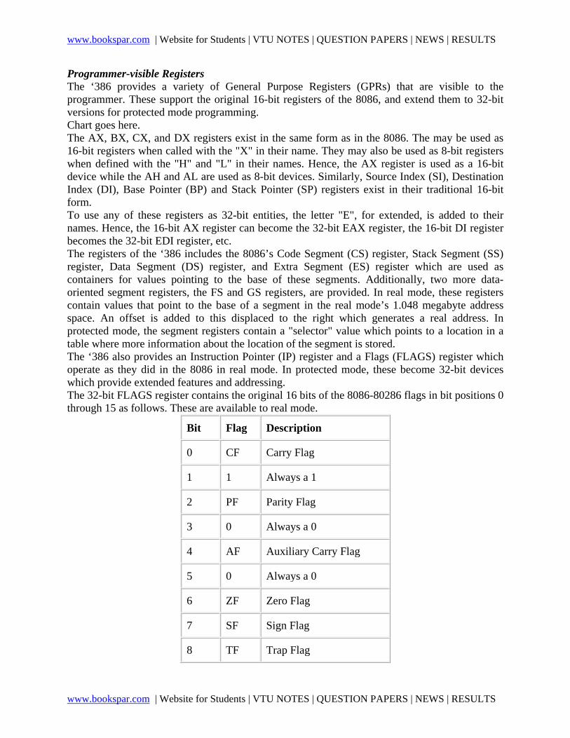
Programmer-visible Registers The ‘386 provides a variety of General Purpose Registers (GPRs) that are visible to the programmer. These support the original 16-bit registers of the 8086, and extend them to 32-bit versions for protected mode programming. Chart goes here. The AX, BX, CX, and DX registers exist in the same form as in the 8086. The may be used as 16-bit registers when called with the "X" in their name. They may also be used as 8-bit registers when defined with the "H" and "L" in their names. Hence, the AX register is used as a 16-bit device while the AH and AL are used as 8-bit devices. Similarly, Source Index (SI), Destination Index (DI), Base Pointer (BP) and Stack Pointer (SP) registers exist in their traditional 16-bit form. To use any of these registers as 32-bit entities, the letter "E", for extended, is added to their names. Hence, the 16-bit AX register can become the 32-bit EAX register, the 16-bit DI register becomes the 32-bit EDI register, etc. The registers of the ‘386 includes the 8086’s Code Segment (CS) register, Stack Segment (SS) register, Data Segment (DS) register, and Extra Segment (ES) register which are used as containers for values pointing to the base of these segments. Additionally, two more data-oriented segment registers, the FS and GS registers, are provided. In real mode, these registers contain values that point to the base of a segment in the real mode’s 1.048 megabyte address space. An offset is added to this displaced to the right which generates a real address. In protected mode, the segment registers contain a "selector" value which points to a location in a table where more information about the location of the segment is stored. The ‘386 also provides an Instruction Pointer (IP) register and a Flags (FLAGS) register which operate as they did in the 8086 in real mode. In protected mode, these become 32-bit devices which provide extended features and addressing. The 32-bit FLAGS register contains the original 16 bits of the 8086-80286 flags in bit positions 0 through 15 as follows. These are available to real mode.
Bit Flag Description
0 CF Carry Flag
1 1 Always a 1
2 PF Parity Flag
3 0 Always a 0
4 AF Auxiliary Carry Flag
5 0 Always a 0
6 ZF Zero Flag
7 SF Sign Flag
8 TF Trap Flag
www.bookspar.com | Website for Students | VTU NOTES | QUESTION PAPERS | NEWS | RESULTS
www.bookspar.com | Website for Students | VTU NOTES | QUESTION PAPERS | NEWS | RESULTS
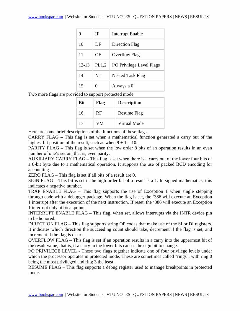
9 IF Interrupt Enable
10 DF Direction Flag
11 OF Overflow Flag
12-13 PL1,2 I/O Privilege Level Flags
14 NT Nested Task Flag
15 0 Always a 0
Two more flags are provided to support protected mode.
Bit Flag Description
16 RF Resume Flag
17 VM Virtual Mode
Here are some brief descriptions of the functions of these flags. CARRY FLAG – This flag is set when a mathematical function generated a carry out of the highest bit position of the result, such as when 9 + 1 = 10. PARITY FLAG – This flag is set when the low order 8 bits of an operation results in an even number of one’s set on, that is, even parity. AUXILIARY CARRY FLAG – This flag is set when there is a carry out of the lower four bits of a 8-bit byte due to a mathematical operation. It supports the use of packed BCD encoding for accounting. ZERO FLAG – This flag is set if all bits of a result are 0. SIGN FLAG – This bit is set if the high-order bit of a result is a 1. In signed mathematics, this indicates a negative number. TRAP ENABLE FLAG – This flag supports the use of Exception 1 when single stepping through code with a debugger package. When the flag is set, the ‘386 will execute an Exception 1 interrupt after the execution of the next instruction. If reset, the ‘386 will execute an Exception 1 interrupt only at breakpoints. INTERRUPT ENABLE FLAG – This flag, when set, allows interrupts via the INTR device pin to be honored. DIRECTION FLAG – This flag supports string OP codes that make use of the SI or DI registers. It indicates which direction the succeeding count should take, decrement if the flag is set, and increment if the flag is clear. OVERFLOW FLAG – This flag is set if an operation results in a carry into the uppermost bit of the result value, that is, if a carry in the lower bits causes the sign bit to change. I/O PRIVILEGE LEVEL - These two flags together indicate one of four privilege levels under which the processor operates in protected mode. These are sometimes called "rings", with ring 0 being the most privileged and ring 3 the least. RESUME FLAG – This flag supports a debug register used to manage breakpoints in protected mode.
www.bookspar.com | Website for Students | VTU NOTES | QUESTION PAPERS | NEWS | RESULTS
www.bookspar.com | Website for Students | VTU NOTES | QUESTION PAPERS | NEWS | RESULTS
VIRTUAL MODE – This flag supports the third mode of operation of the processor, Virtual 8086 mode. Once in protected mode, if set, this flag causes the processor to switch to virtual 8086 mode. Programmer-invisible Registers To support protected mode, a variety of other registers are provided that are not accessible by the programmer. In real mode, the programmer can see and reference the segment registers CS, SS, DS, ES, FS, and GS as 16-bit entities. The contents of these registers are shifted four bit positions to the left, then added to a 16-bit offset provided by the program. The resulting 20-bit value is the real address of the data to be accessed at that moment. This allows a real address space of 220 or 1.048 megabytes. In this space, all segments are limited to 64K maximum size. In protected mode, segments may from 1 byte to 4.3 gigabytes in size. Further, there is more information that is needed than in real mode. Therefore, the segment registers of real mode become holders for "selectors", values which point to a reference in a table in memory that contains more detail about the area in the desired segment. Also, a set of "Descriptor Registers" is provided, one for each segment register. These contain the physical base address of the segment, the segment limit (or the size of the segment relative to the base), and a group of other data items that are loaded from the descriptor table. In protected mode, when a segment register is loaded with a new selector, that selector references the table that has previously been set up, and the descriptor register for that segment register is given the new information from the table about that segment. During the course of program execution, addressing references to that segment are made using the descriptor register for that segment. Four Control Registers CR0 – CR3 are provided to support specific hardware needs. CR0 is called the Machine Control Register and contains several bits that were derived in the 80286. These are: PAGING ENABLED, bit 31 – This bits when set enables the on-chip paging unit for virtual memory. TASK SWITCHED, bit 3 – This bit is set when a task switch is performed. EMULATE COPROCESSOR, bit 2 – This bit causes all coprocessor OP codes to cause a Coprocessor-Not-Found exception. This is turn will cause 80387 math coprocessor instructions to have to be interpreted by software. MONITOR COPROCESSOR, bit 1 – Works with the TS bit above to synchronize the coprocessor. PROTECTION ENABLED, bit 0 – This bit enables the shift to protected mode from real mode. System Address Registers Four special registers are provided to reference the tables needed to support protected mode. These tables are the Global Descriptor Table (GDT), the Interrupt Descriptor Table (IDT), the Local Descriptor Table (LDT) , and the Task State Segment (TSS). The addresses of these tables are stored in four special registers called the Global Descriptor Table Register (GDTR), the Interrupt Descriptor Table Register (IDTR), the Local Descriptor Table Register (LDTR), and the Task State Segment Register (TR). These tables and registers will be discussed more fully below. Briefly, the GDTR and IDTR hold the 32-bit linear base address and the 16-bit limit of the GDT and IDT, respectively. Both of these tables are global in nature and so may be located anywhere, including in paged virtual memory. These tables are not located using segment registers. The LDTR and TR hold 16-bit selector values for the LDT descriptor and the TSS descriptor, respectively. The LDT and TSS are task-specific segments, tied to individual tasks within the
www.bookspar.com | Website for Students | VTU NOTES | QUESTION PAPERS | NEWS | RESULTS
www.bookspar.com | Website for Students | VTU NOTES | QUESTION PAPERS | NEWS | RESULTS
system. Selectors to locate these segments are stored in system segment registers. These selectors point to the table areas and work in conjunction with two descriptor registers that contain a 32-bit linear base address for the table, a 32-bit segment limit, and some attribute bytes. This is in concert with the approach for the programmer-visible segment registers. MEMORY ORGANIZATION In the 80386, data may take the physical form of an 8-bit byte, a 16-bit word, or a 32-bit double word. The electrical organization of the memory connections to the processor follow this model. For a word, the high-order byte is in the higher-addressed of the two bytes, while the low-order byte is in the lower-addressed address. In the case of a 32-bit double word, the highest-most byte is located in the highest address, and the lowest byte is located in the lowest address. The address of the lowest byte is the address of the word or double word. The 80386 also supports two other memory units. These are segments and pages. Segments can be variable in length, and this supports a programmer’s approach to arranging code and data in some sort of logical order for the work being done. Pages in this case are 4,096 bytes in length, and these support the use of physical memory management, e.g., virtual memory. Intel defines three distinct address spaces. These are physical, logical, and linear. The programmer sees and works with the logical address space. It is constructed of the information contained in a selector’s table reference plus the addition of various offsets and indexes created by the addressing modes of the program’s instructions. The programmer does not care about the amount of memory consumed – he/she considers it to be "virtually" infinite in size. In fact, since each task in an 80386 can have 16K selectors, and since offsets can be as much as 4 gigabytes in size, the programmer can work with as much as 64 terabytes of memory. The segmentation unit of the processor translates the logical address space of the programmer to the 32-bit linear address space. If the paging unit is not enabled, the linear address space and the physical address space are one and the same, and the linear address space is sent directly to the device pins, thus becoming the physical address. If the paging unit is in use, then it will further modify the linear address space to a different address space that may engage outside storage to implement the memory that doesn’t really exist in the system. The primary difference between real and protected mode is the way in which the segmentation unit performs the translation between logical and linear addresses. Just like the 8086, in real mode the 80386 shifts the contents of the segment register left four bit positions, then adds the offset to create a 20-bit linear address which is the same as the physical address (in the 8086, there is no paging unit, so the linear and the physical addresses are always the same). In protected mode, every selector has a linear base address connected with it. This linear base address is stored in either the GDT or an LDT for the segment. From the table, the selector’s linear base address is added to the offset from the program’s instructions to create the final linear address. If paging is off, this is also the physical address. If paging is on, further modification occurs to create the final physical address from the logical address. REAL MODE ARCHITECTURE When the 80386 is reset, it assumes real mode. Real mode has the same base architecture as the 8086. The addressing mechanism, memory size, and interrupt handling are all identical to the real mode of the 80286. However, the system allows access to the 32-bit register set. Almost all of the 80386 instructions are accessible in real mode. The default operand size is 16 bits. To use the 32-bit registers and addressing modes of the 80386 in real mode, override prefixes must be used. The segment size in real mode is a maximum of 64K. Because of the paging feature
www.bookspar.com | Website for Students | VTU NOTES | QUESTION PAPERS | NEWS | RESULTS
www.bookspar.com | Website for Students | VTU NOTES | QUESTION PAPERS | NEWS | RESULTS
available for protected mode, it is not possible to use the lock prefix on repetitive string instructions. In real mode, the memory size is limited to one megabyte, using addressing lines A2 through A19. The exception to this is that the A20 – A31 lines are available from reset to the first execution of an intersegment jump or call. This allows the ROM holding the power-on reset vector and initialization code to be accessed. There is no paging in real mode, so the linear address is the physical address. The physical address is created by the offset addition of the contents of a particular segment register (CS, DS, SS, or ES) and an offset provided by the analysis of an instruction, such as the contents of an index register (SI or DI). The addition is offset such that the segment register’s contents is added four bit positions to the left of the offset’s value, thus: Illustration Hence, although the segment registers and the offsets can contain no more than 16 bits each, the sum generated is 20 bits long, sufficient to access any location with the 1.048 megabyte address space of real mode. Since the segment register contents is always shifted four bits to the left, segments must always begin on 16-byte boundaries. Segments may be overlapped, that is, there is no restriction to segment registers containing values that are within another segment’s 64-K address space. This allows programmers to use only what is needed for a small program. There are two reserved areas of the memory map. The interrupt vectors occupy the first 1,024 bytes of them memory space, addresses 0 to 3FFh. This permits 256 4-byte jump vectors as in the 8086. Also, locations FFFFFFF0h through FFFFFFFFh are reserved for the reset vector. The system will initially attempt to execute an instruction at FFFFFFF0h following the clearing of reset. The Halt (HLT) instruction will cause the processor to stop execution and keeps it from using its local bus. Halt can be cleared by three methods:
1. A non-maskable interrupt (NMI); 2. A regular interrupt (INTR) with interrupts enabled; 3. A system reset.
PROTECTED MODE ARCHTECTURE The 80386 is most impressive when running in protected mode. The linear address space can be as great as 232 (4294967295) bytes. With the paging unit enabled, the limit is 246 or about 64 terabytes. The device can run all 8086 and 80286 code. It provides a memory management and a hardware-assisted protection mechanism that keeps one program’s execution from interfering with another. Additional instructions are provided to support multitasking. The programmer sees an expanded address space available to her/him, and different addressing scheme. Memory Segmentation Memory segmentation in protected mode uses a segment base value and an offset in the manner of real mode. However, because of the increased size of the address space now available, a more complex arrangement is used. The segment register now contains a value called a selector. This is a 16-bit value which contains an offset into a table. This table, called a descriptor table, contains descriptors which are 8-byte values that describe more about the segment in question. Two tables provided are the Global Descriptor Table (GDT) and the Local Descriptor Table (LDT). The GDT contains information about segments that are global in nature, that is, available to all programs and normally used most heavily by the operating system. The LDT contains
www.bookspar.com | Website for Students | VTU NOTES | QUESTION PAPERS | NEWS | RESULTS
www.bookspar.com | Website for Students | VTU NOTES | QUESTION PAPERS | NEWS | RESULTS
descriptors that are application specific. Both of these tables have a limit of 64K, that is, 8,192 8-byte entries. There is also an Interrupt Descriptor Table (IDT) that contains information about segments containing code used in servicing interrupts. This table has a maximum of 256 entries. The upper 13 bits of the selector are used as an offset into the descriptor table to be used. The lower 3 bits are:
• TI, a table selection bit – 0 = use the GDT, 1 = use the LDT. • RPL, Requested Privilege Level bits = 00 is the highest privilege level, 11 is the lowest.
The selector identifies the table to be used and the offset into that table where a set of descriptor bytes identifies the segment specifically. Each table can be 64K bytes in size, so if there are 8 bytes per table entry, a total of 8,192 entries can be held in one table at a given time. The contents of a descriptor are: Bytes 0 and 1 – A 16-bit value that is connected to bits 0 – 3 of byte 6 to form the uppermost offset, or limit, allowed for the segment. This 20 bit limit means that a segment can be between 1 byte and 1 megabyte in size. See the discussion of the granularity bit below. Bytes 2 and 3 – A 16-bit value connected to byte 4 and byte 7 to form a 32-bit base value for the segment. This is the value added to the offset provided by the program execution to form the linear address. AV bit – Segment available bit, where AV=0 indicates not available and AV=1 indicates available. D bit – If D=0, this indicates that instructions use 16-bit offsets and 16-bit registers by default. If D=1, the instructions are 32-bit by default. Granularity (G) bit – If G=0, the segments are in the range of 1 byte to 1 megabyte. If G=1, the segment limit value is multiplied by 4K, meaning that the segments can have a minimum of 4K bytes and a maximum limit of 4 gigabytes in steps of 4K. Byte 5, Access Rights byte – This byte contains several flags to further define the segment:
• Bit 0, Access bit – A=0 indicates that the segment has not been accessed; A=1 indicates that the segment has been accessed (and is now "dirty").
• Bits 1, R/W bit; bit 2, ED/C bit; and bit 3, E bit. If bit 3 = 0, then the descriptor references a data segment and the other bits are interpreted as follows: bit 2, interpreted as the ED bit, if 0, indicates that the segment expands upward, as in a data segment; if 1, indicates that the segment expands in the downward direction, as in a stack segment; bit 1, the R/W bit, if 0, indicates that the segment may not be written, while if 1 indicates that the segment is writeable. If bit 3 = 1, then the descriptor references a code segment and the other bits are interpreted as follows: bit 2, interpreted as the C bit, if 0, indicates that we should ignore the descriptor privilege for the segment, while if 1 indicates that privilege must be observed; bit 1, the R/W bit, if 0, indicates that the code segment may not be read, while if 1 indicates that the segment is readable.
• Bit 4, System bit – If 0, this is a system descriptor; if 1, this is a regular code or data segment.
• Bits 5 and 6, Descriptor Privilege Level (DPL) bits – These two bits identify the privilege level of the descriptor.
www.bookspar.com | Website for Students | VTU NOTES | QUESTION PAPERS | NEWS | RESULTS
www.bookspar.com | Website for Students | VTU NOTES | QUESTION PAPERS | NEWS | RESULTS
• Bit 7, Segment Valid (P) bit – If 0, the descriptor is undefined. If 1, the segment contains a valid base and limit.
Use the illustration below to follow the flow of address translation. Numbers in circles on the drawing match those below. File goes here
1. The execution of an instruction causes a request to access memory. The segment portion of the address to be used is represented by a selector value. This is loaded into the segment register. Generally, this value is not changed too often, and is controlled by the operating system.
2. The selector value in the segment register specifies a descriptor table and points to one of 8,192 descriptor areas. These contain 8 bytes that identify the base of the real segment, its limit, and various access and privilege information.
3. The base value in the descriptor identifies the base address of the segment to be used in linear address space.
4. The limit value in the descriptor identifies the offset of the top of the segment area from the base.
5. The offset provided by the instruction is used to identify the specific location of the desired byte(s) in linear address space, relative to the base value.
The byte(s) thus specified are read or written as dictated by the instruction. Program Invisible Registers Several additional registers are provided that are normally invisible to the programmer but are required by the hardware of the processor to expedite its functions. Each of the segment registers (CS, DS, SS, ES, FS, and GS) have an invisible portion that is called a cache. The name is used because they store information for short intervals – they are not to be confused with the L1 or L2 cache of the external memory system. The program invisible portions of the segment registers are loaded with the base value, the limit value, and the access information of the segment each time the segment register is loaded with a new selector. This allows just one reference to the descriptor table to be used for multiple accesses to the same segment. It is not necessary to reference the descriptor table again until the contents of the segment register is changed indicating a new segment of that type is being accessed. This system allows for faster access to the main memory as the processor can look in the cache for the information rather than having to access the descriptor table for every memory reference to a segment. The Global Descriptor Table Register (GDTR) and the Interrupt Descriptor Table Register (IDTR) contain the base address of the descriptor tables themselves and their limits, respectively. The limit is a 16-bit value because the maximum size of the tables is 64K. System Descriptors The Local Descriptor Table Register contains a 16-bit wide selector only. This value references a system descriptor, which is similar to that as described above, but which contains a type field that identifies one of 16 types of descriptor (specifically type 0010) that can exist in the system. This system descriptor in turn contains base and limit values that point to the LDT in use at the moment. In this way, there is one global descriptor table for the operating system, but there can be many local tables for individual applications or tasks if needed.
www.bookspar.com | Website for Students | VTU NOTES | QUESTION PAPERS | NEWS | RESULTS
www.bookspar.com | Website for Students | VTU NOTES | QUESTION PAPERS | NEWS | RESULTS
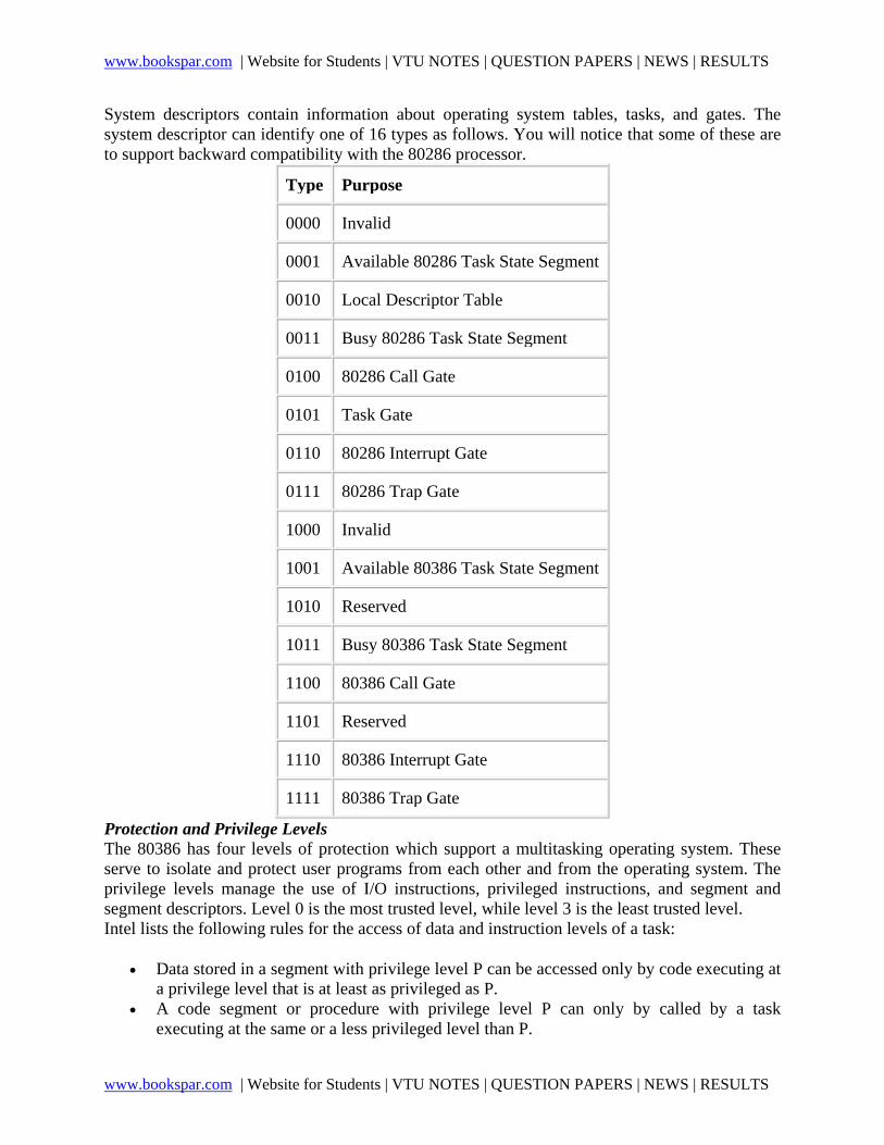
System descriptors contain information about operating system tables, tasks, and gates. The system descriptor can identify one of 16 types as follows. You will notice that some of these are to support backward compatibility with the 80286 processor.
Type Purpose
0000 Invalid
0001 Available 80286 Task State Segment
0010 Local Descriptor Table
0011 Busy 80286 Task State Segment
0100 80286 Call Gate
0101 Task Gate
0110 80286 Interrupt Gate
0111 80286 Trap Gate
1000 Invalid
1001 Available 80386 Task State Segment
1010 Reserved
1011 Busy 80386 Task State Segment
1100 80386 Call Gate
1101 Reserved
1110 80386 Interrupt Gate
1111 80386 Trap Gate
Protection and Privilege Levels The 80386 has four levels of protection which support a multitasking operating system. These serve to isolate and protect user programs from each other and from the operating system. The privilege levels manage the use of I/O instructions, privileged instructions, and segment and segment descriptors. Level 0 is the most trusted level, while level 3 is the least trusted level. Intel lists the following rules for the access of data and instruction levels of a task:
• Data stored in a segment with privilege level P can be accessed only by code executing at a privilege level that is at least as privileged as P.
• A code segment or procedure with privilege level P can only by called by a task executing at the same or a less privileged level than P.
www.bookspar.com | Website for Students | VTU NOTES | QUESTION PAPERS | NEWS | RESULTS
www.bookspar.com | Website for Students | VTU NOTES | QUESTION PAPERS | NEWS | RESULTS
At any point in time, a task can be operating at any of the four privilege levels. This is called the task’s Current Privilege Level (CPL). A task’s privilege level may only be changed by a control transfer through a gate descriptor to a code segment with a different privilege level. The lower two bits of selectors contain the Requested Privilege Level (RPL). When a change of selector is made, the CPL of the task and the RPL of the new selector are compared. If the RPL is more privileged than the CPL, the CPL determines the level at which the task will continue. If the CPL is more privileged than the RPL, the RPL value will determine the level for the task. Therefore, the lowest privilege level is selected at the time of the change. The purpose of this function is to ensure that pointers passed to an operating system procedure are not of a higher privilege than the procedure that originated the pointer. Gates Gates are used to control access to entry points within the target code segment. There are four types:
• Call Gates – those associated with Call, Jump, Return and similar operations codes. They provide a secure method of privilege transfer within a task.
• Task Gates – those involved with task switching. • Interrupt Gates – those involved with normal interrupt service needs. • Trap Gates – those involved with error conditions that cause major faults in the
execution.
A gate is simply a small block of code in a segment that allows the system to check for privilege level violations and to control entry to the operating system services. The gate code lives in a segment pointed to by special descriptors. These descriptors contain base and offset values to locate the code for the gate, a type field, a two-bit Default Privilege Level (DPL) and a five-bit word count field. This last is used to indicate the number of words to be copied from the stack of the calling routine to that of the called routine. This is used only in Call Gates when there is a change in privilege level required. Interrupt and Trap gates work similarly except that there is no pushing of parameters onto the stack. For interrupt gates, further interrupts are disabled. Gates are part of the operating system and are mainly of interest to system programmers. Task Switching An important part of any multitasking system is the ability to switch between tasks quickly. Tasks may be anything from I/O routines in the operating system to parts of programs written by you. With only a single processor available in the typical PC, it is essential that when the needs of the system or operator are such that a switch in tasks is needed, this be done quickly. The 80386 has a hardware task switch instruction. This causes the machine to save the entire current state of the processor, including all the register contents, address space information, and links to previous tasks. It then loads a new execution state, performs protection checks, and begins the new task, all in about 17 microseconds. The task switch is invoked by executing an intersegment jump or call which refers to a Task Switch Segment (TSS) or a task gate descriptor in the LDT or GDT. An INT n instruction, exception, trap, or external interrupt may also invoke a task switch via a task gate descriptor in the associated IDT. Each task must have an associated Task Switch Segment. This segment contains an image of the system’s conditions as they exist for that task. The TSS for the current task, the one being executed by the system at the moment, is identified by a special register called the Task Switch Segment Register (TR). This register contains a selector referring to the task state segment
www.bookspar.com | Website for Students | VTU NOTES | QUESTION PAPERS | NEWS | RESULTS
www.bookspar.com | Website for Students | VTU NOTES | QUESTION PAPERS | NEWS | RESULTS
descriptor that defines the current TSS. A hidden base and limit register connected to the TR are loaded whenever TR is updated. Returning from a task is accomplished with the IRET instruction which returns control to the task that was interrupted with the switch. The current task’s segment is stored and the previous task’s segment is used to bring it into the current task. Control Registers The 80386 has four "Control Registers" called CR0 through CR3. CR0 contains several bit flags as follows: PG – When set to 1, causes the translation of linear addresses to physical addresses. Indicates that paging is enabled and virtual memory is being used. ET – When set to 1, indicates that the 80387 math coprocessor is in use. TS – When set to 1, indicates that the processor has switched tasks. EM – When set to 1, causes a type 7 interrupt for the ESC (escape) instruction for the math coprocessor. MP – When set to 1, indicates that the math coprocessor is present in the system. PE – Selects protected mode of operation. CR 1 is not used by the ‘386. CR2 contains page fault linear addresses for the virtual memory manager. CR3 contains a pointer to the base of the page directory for virtual memory management. Switching to Protected Mode At reset, the 80386 begins operation in Real Mode. This is to allow setup of various conditions before the switch to Protected Mode is made. The actual switch is accomplished by setting the PE bit in CR0. The following steps are needed.
1. Initialize the interrupt descriptor table to contain valid interrupt gates for at least the first 32 interrupt types. The IDT can contain 256 8-byte gates.
2. Set up the GDT so that it contains a null descriptor at position 0, and valid descriptors for at least one code, one data, and one stack segment.
3. Switch to protected mode by setting PE to 1. 4. Execute a near JMP to flush the internal instruction queue and to load the TR with the
base TSS descriptor. 5. Load all the data selectors with initial values. 6. The processor is now running in Protected Mode using the given GDT and IDT.
In the case of a multitasking system, an alternate approach is to load the GDT with at least two TSS descriptors in addition to the code and data descriptors needed for the first task. The first JMP following the setting of the PE bit will cause a task switch that loads all the data needed from the TSS of the first task to be entered. Multitasking is then initialized. VIRTUAL 8086 MODE The third mode of operation provided by the 80386 is that of Virtual 8086 Mode. Once in protected mode, one or more virtual 8086 tasks can be initiated. Virtual 8086 tasks appear to be like real mode. The task is limited to 1 megabyte of memory whose address space is located at 0 through FFFFFh; the segment registers are used as they are in real mode (no selectors or lookup tables are involved). Each of the virtual 8086 tasks are given a certain amount of time using a time-slice algorithm typical of mainframes (timesharing). The software for such tasks is written as if they were to run in a real mode address space. However, using paging, multiple such sessions can be located anywhere in the virtual memory space of the 80386.
www.bookspar.com | Website for Students | VTU NOTES | QUESTION PAPERS | NEWS | RESULTS
www.bookspar.com | Website for Students | VTU NOTES | QUESTION PAPERS | NEWS | RESULTS
Windows NT and OS/2 use this technique to support one or more DOS sessions, or low-priority utilities such as a print spooler. VIRTUAL MEMORY AND PAGING Using selectors and tables, the 80386 generates what Intel defines as a linear address as a means of locating data or instructions for real mode or for the current task in protected mode. If the system is not using virtual memory or paging, then the linear address is the physical address of the desired data or bytes, and is forwarded to the pins of the device to become the physical address. Paging allows a level of interpretation to be inserted between the linear address and the physical address. The linear address is passed to the paging unit, and it in turn converts it to a physical address that will be different than the linear one. This allows several options, including 1) mapping a linear address to some other physical address according to the needs of a multitasking operating system to place tasks at convenient locations, or 2) mapping linear addresses to memory that does not exist in the system, but might be replaced by disk space. Paging logically divides the available virtual space into "pages" that are 4Kbytes in size. Three elements are needed to implement paging. These are the page directory, the page table, and the actual physical memory page. Values in these tables are obtained by combining parts of the linear address with values from the tables which point to other values. The page directory is a table of as many as 1,024 4-byte entries. (This is a maximum number; most systems use far fewer entries.) The base of the page directory is determined by the value contained in CR3. An offset into the directory is created from the uppermost 10 bits (positions 22-31) of the linear address. At this offset in the directory, we find a pointer to the base of a page table. This means that there can be as many as 1,024 page tables in a system. There are 1,024 entries possible in each page table. The middle 10 bits of the linear address (bit positions 12 through 21) are used as a offset into the selected page table. The value thus determined is a pointer to the base of a 4K memory page. The offset into the page to located the specific data needed is contained in the lower 12 bits of the linear address. The entries in the page directory and page tables are identical. They contain 10 bits of addressing, and the following flags: D or DIRTY bit: This bit is not used in the page directory. In the page table entries, it indicates that the 4K area defined by this entry has been written to, and so must be saved (as to disk) if the area is to be reused for something else. A or ACCESSED bit: This bit is set to a 1 when the processor accesses the 4K page. R/W or Read/Write and U/S or User/Supervisor bits: These are used in conjunction with privilege management. P or PRESENT bit: This bit when set to 1 indicates that the referenced page is present in memory. If 0, it can be used to indicate that the page is not in RAM, e.g., is on disk. Performance of the paging system would be affected if the system needed to reference memory tables each time a reference to RWM was made. To offset this, a Translation Lookaside Buffer (TLB) is provided. This is a 4-way set-associative cache that contains entries for the last 32 pages needed by the processor. This provides immediate information about 98% of the time, causing only 2% of memory accesses to make the page directory-page table translation. HARDWARE HIGHLIGHTS The instructor will provide you with illustrations of the timing sequences for the various read and write cycles available on the 80386. There are two items of interest that we note here. Address Pipelining
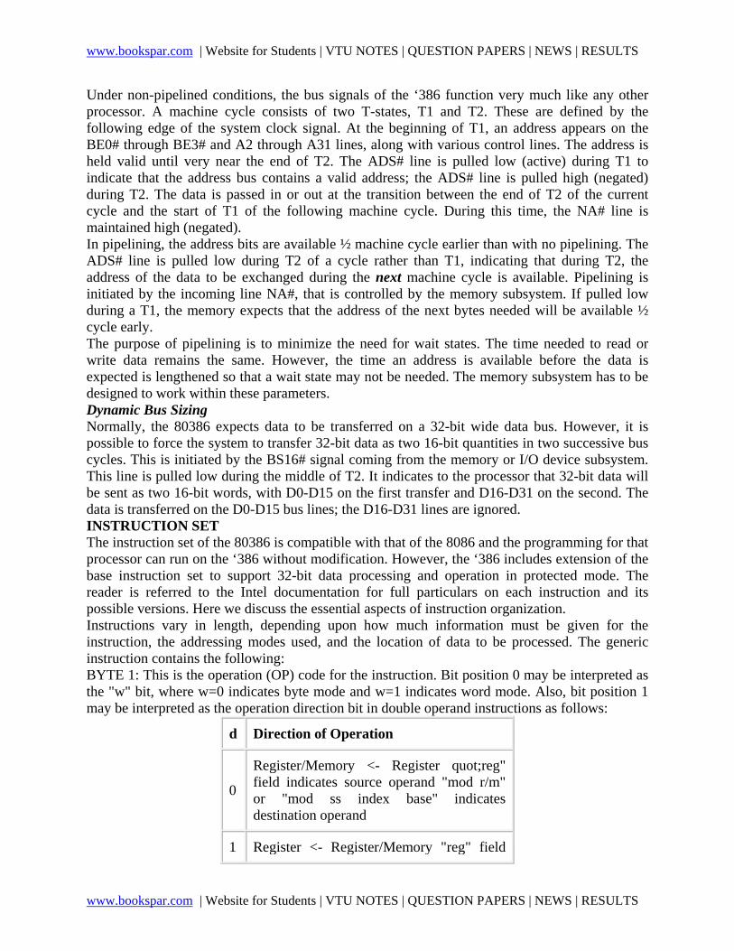
www.bookspar.com | Website for Students | VTU NOTES | QUESTION PAPERS | NEWS | RESULTS
www.bookspar.com | Website for Students | VTU NOTES | QUESTION PAPERS | NEWS | RESULTS
Under non-pipelined conditions, the bus signals of the ‘386 function very much like any other processor. A machine cycle consists of two T-states, T1 and T2. These are defined by the following edge of the system clock signal. At the beginning of T1, an address appears on the BE0# through BE3# and A2 through A31 lines, along with various control lines. The address is held valid until very near the end of T2. The ADS# line is pulled low (active) during T1 to indicate that the address bus contains a valid address; the ADS# line is pulled high (negated) during T2. The data is passed in or out at the transition between the end of T2 of the current cycle and the start of T1 of the following machine cycle. During this time, the NA# line is maintained high (negated). In pipelining, the address bits are available ½ machine cycle earlier than with no pipelining. The ADS# line is pulled low during T2 of a cycle rather than T1, indicating that during T2, the address of the data to be exchanged during the next machine cycle is available. Pipelining is initiated by the incoming line NA#, that is controlled by the memory subsystem. If pulled low during a T1, the memory expects that the address of the next bytes needed will be available ½ cycle early. The purpose of pipelining is to minimize the need for wait states. The time needed to read or write data remains the same. However, the time an address is available before the data is expected is lengthened so that a wait state may not be needed. The memory subsystem has to be designed to work within these parameters. Dynamic Bus Sizing Normally, the 80386 expects data to be transferred on a 32-bit wide data bus. However, it is possible to force the system to transfer 32-bit data as two 16-bit quantities in two successive bus cycles. This is initiated by the BS16# signal coming from the memory or I/O device subsystem. This line is pulled low during the middle of T2. It indicates to the processor that 32-bit data will be sent as two 16-bit words, with D0-D15 on the first transfer and D16-D31 on the second. The data is transferred on the D0-D15 bus lines; the D16-D31 lines are ignored. INSTRUCTION SET The instruction set of the 80386 is compatible with that of the 8086 and the programming for that processor can run on the ‘386 without modification. However, the ‘386 includes extension of the base instruction set to support 32-bit data processing and operation in protected mode. The reader is referred to the Intel documentation for full particulars on each instruction and its possible versions. Here we discuss the essential aspects of instruction organization. Instructions vary in length, depending upon how much information must be given for the instruction, the addressing modes used, and the location of data to be processed. The generic instruction contains the following: BYTE 1: This is the operation (OP) code for the instruction. Bit position 0 may be interpreted as the "w" bit, where w=0 indicates byte mode and w=1 indicates word mode. Also, bit position 1 may be interpreted as the operation direction bit in double operand instructions as follows:
d Direction of Operation
0
Register/Memory <- Register quot;reg" field indicates source operand "mod r/m" or "mod ss index base" indicates destination operand
1 Register <- Register/Memory "reg" field
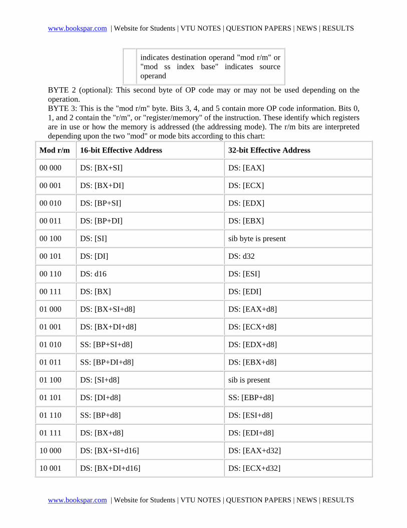
www.bookspar.com | Website for Students | VTU NOTES | QUESTION PAPERS | NEWS | RESULTS
www.bookspar.com | Website for Students | VTU NOTES | QUESTION PAPERS | NEWS | RESULTS
indicates destination operand "mod r/m" or "mod ss index base" indicates source operand
BYTE 2 (optional): This second byte of OP code may or may not be used depending on the operation. BYTE 3: This is the "mod r/m" byte. Bits 3, 4, and 5 contain more OP code information. Bits 0, 1, and 2 contain the "r/m", or "register/memory" of the instruction. These identify which registers are in use or how the memory is addressed (the addressing mode). The r/m bits are interpreted depending upon the two "mod" or mode bits according to this chart:
Mod r/m 16-bit Effective Address 32-bit Effective Address
00 000 DS: [BX+SI] DS: [EAX]
00 001 DS: [BX+DI] DS: [ECX]
00 010 DS: [BP+SI] DS: [EDX]
00 011 DS: [BP+DI] DS: [EBX]
00 100 DS: [SI] sib byte is present
00 101 DS: [DI] DS: d32
00 110 DS: d16 DS: [ESI]
00 111 DS: [BX] DS: [EDI]
01 000 DS: [BX+SI+d8] DS: [EAX+d8]
01 001 DS: [BX+DI+d8] DS: [ECX+d8]
01 010 SS: [BP+SI+d8] DS: [EDX+d8]
01 011 SS: [BP+DI+d8] DS: [EBX+d8]
01 100 DS: [SI+d8] sib is present
01 101 DS: [DI+d8] SS: [EBP+d8]
01 110 SS: [BP+d8] DS: [ESI+d8]
01 111 DS: [BX+d8] DS: [EDI+d8]
10 000 DS: [BX+SI+d16] DS: [EAX+d32]
10 001 DS: [BX+DI+d16] DS: [ECX+d32]
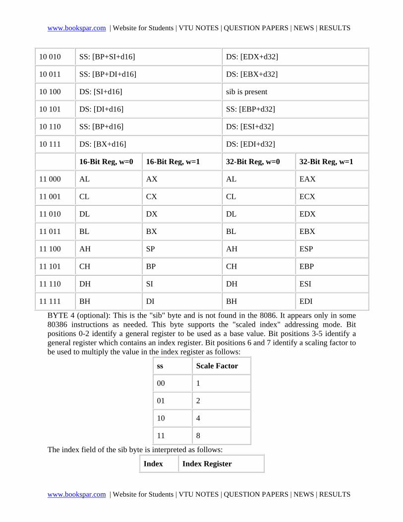
www.bookspar.com | Website for Students | VTU NOTES | QUESTION PAPERS | NEWS | RESULTS
www.bookspar.com | Website for Students | VTU NOTES | QUESTION PAPERS | NEWS | RESULTS
10 010 SS: [BP+SI+d16] DS: [EDX+d32]
10 011 SS: [BP+DI+d16] DS: [EBX+d32]
10 100 DS: [SI+d16] sib is present
10 101 DS: [DI+d16] SS: [EBP+d32]
10 110 SS: [BP+d16] DS: [ESI+d32]
10 111 DS: [BX+d16] DS: [EDI+d32]
16-Bit Reg, w=0 16-Bit Reg, w=1 32-Bit Reg, w=0 32-Bit Reg, w=1
11 000 AL AX AL EAX
11 001 CL CX CL ECX
11 010 DL DX DL EDX
11 011 BL BX BL EBX
11 100 AH SP AH ESP
11 101 CH BP CH EBP
11 110 DH SI DH ESI
11 111 BH DI BH EDI
BYTE 4 (optional): This is the "sib" byte and is not found in the 8086. It appears only in some 80386 instructions as needed. This byte supports the "scaled index" addressing mode. Bit positions 0-2 identify a general register to be used as a base value. Bit positions 3-5 identify a general register which contains an index register. Bit positions 6 and 7 identify a scaling factor to be used to multiply the value in the index register as follows:
ss Scale Factor
00 1
01 2
10 4
11 8
The index field of the sib byte is interpreted as follows:
Index Index Register
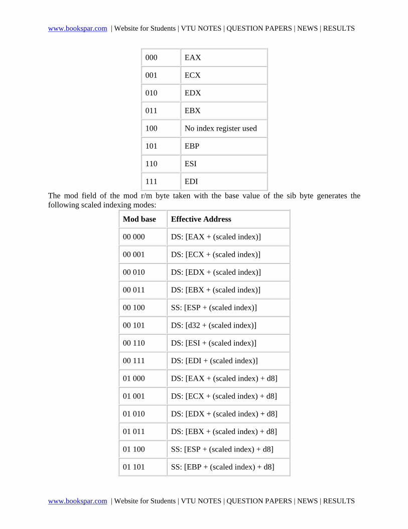
www.bookspar.com | Website for Students | VTU NOTES | QUESTION PAPERS | NEWS | RESULTS
www.bookspar.com | Website for Students | VTU NOTES | QUESTION PAPERS | NEWS | RESULTS
000 EAX
001 ECX
010 EDX
011 EBX
100 No index register used
101 EBP
110 ESI
111 EDI
The mod field of the mod r/m byte taken with the base value of the sib byte generates the following scaled indexing modes:
Mod base Effective Address
00 000 DS: [EAX + (scaled index)]
00 001 DS: [ECX + (scaled index)]
00 010 DS: [EDX + (scaled index)]
00 011 DS: [EBX + (scaled index)]
00 100 SS: [ESP + (scaled index)]
00 101 DS: [d32 + (scaled index)]
00 110 DS: [ESI + (scaled index)]
00 111 DS: [EDI + (scaled index)]
01 000 DS: [EAX + (scaled index) + d8]
01 001 DS: [ECX + (scaled index) + d8]
01 010 DS: [EDX + (scaled index) + d8]
01 011 DS: [EBX + (scaled index) + d8]
01 100 SS: [ESP + (scaled index) + d8]
01 101 SS: [EBP + (scaled index) + d8]
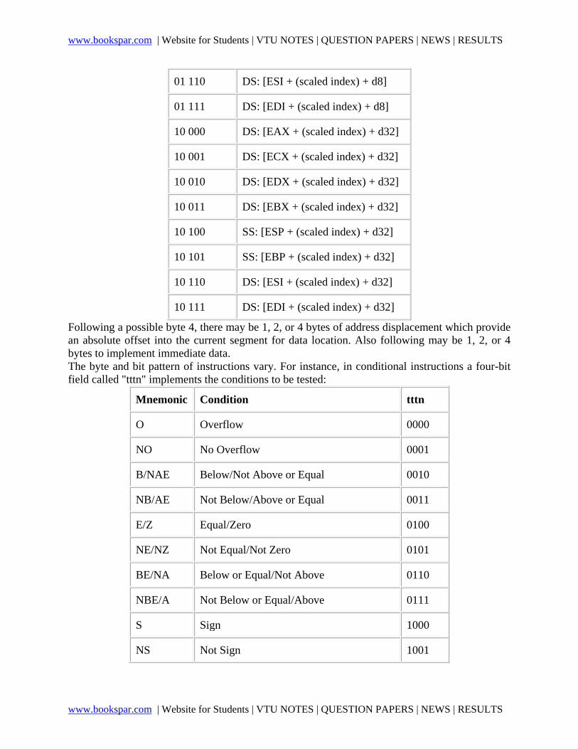
www.bookspar.com | Website for Students | VTU NOTES | QUESTION PAPERS | NEWS | RESULTS
www.bookspar.com | Website for Students | VTU NOTES | QUESTION PAPERS | NEWS | RESULTS
01 110 DS: [ESI + (scaled index) + d8]
01 111 DS: [EDI + (scaled index) + d8]
10 000 DS: [EAX + (scaled index) + d32]
10 001 DS: [ECX + (scaled index) + d32]
10 010 DS: [EDX + (scaled index) + d32]
10 011 DS: [EBX + (scaled index) + d32]
10 100 SS: [ESP + (scaled index) + d32]
10 101 SS: [EBP + (scaled index) + d32]
10 110 DS: [ESI + (scaled index) + d32]
10 111 DS: [EDI + (scaled index) + d32]
Following a possible byte 4, there may be 1, 2, or 4 bytes of address displacement which provide an absolute offset into the current segment for data location. Also following may be 1, 2, or 4 bytes to implement immediate data. The byte and bit pattern of instructions vary. For instance, in conditional instructions a four-bit field called "tttn" implements the conditions to be tested:
Mnemonic Condition tttn
O Overflow 0000
NO No Overflow 0001
B/NAE Below/Not Above or Equal 0010
NB/AE Not Below/Above or Equal 0011
E/Z Equal/Zero 0100
NE/NZ Not Equal/Not Zero 0101
BE/NA Below or Equal/Not Above 0110
NBE/A Not Below or Equal/Above 0111
S Sign 1000
NS Not Sign 1001
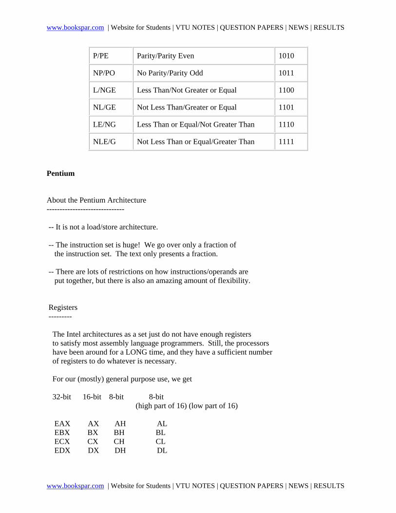
www.bookspar.com | Website for Students | VTU NOTES | QUESTION PAPERS | NEWS | RESULTS
www.bookspar.com | Website for Students | VTU NOTES | QUESTION PAPERS | NEWS | RESULTS
P/PE Parity/Parity Even 1010
NP/PO No Parity/Parity Odd 1011
L/NGE Less Than/Not Greater or Equal 1100
NL/GE Not Less Than/Greater or Equal 1101
LE/NG Less Than or Equal/Not Greater Than 1110
NLE/G Not Less Than or Equal/Greater Than 1111
Pentium About the Pentium Architecture ------------------------------ -- It is not a load/store architecture. -- The instruction set is huge! We go over only a fraction of the instruction set. The text only presents a fraction. -- There are lots of restrictions on how instructions/operands are put together, but there is also an amazing amount of flexibility. Registers --------- The Intel architectures as a set just do not have enough registers to satisfy most assembly language programmers. Still, the processors have been around for a LONG time, and they have a sufficient number of registers to do whatever is necessary. For our (mostly) general purpose use, we get 32-bit 16-bit 8-bit 8-bit (high part of 16) (low part of 16) EAX AX AH AL EBX BX BH BL ECX CX CH CL EDX DX DH DL
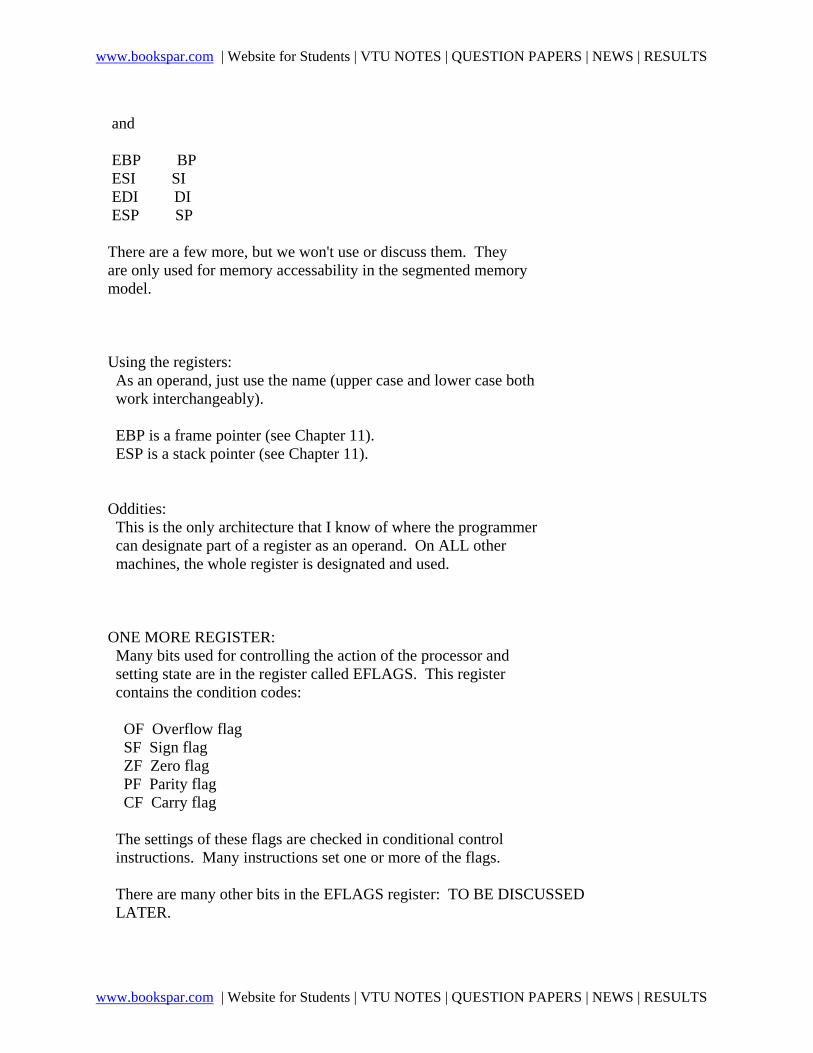
www.bookspar.com | Website for Students | VTU NOTES | QUESTION PAPERS | NEWS | RESULTS
www.bookspar.com | Website for Students | VTU NOTES | QUESTION PAPERS | NEWS | RESULTS
and EBP BP ESI SI EDI DI ESP SP There are a few more, but we won't use or discuss them. They are only used for memory accessability in the segmented memory model. Using the registers: As an operand, just use the name (upper case and lower case both work interchangeably). EBP is a frame pointer (see Chapter 11). ESP is a stack pointer (see Chapter 11). Oddities: This is the only architecture that I know of where the programmer can designate part of a register as an operand. On ALL other machines, the whole register is designated and used. ONE MORE REGISTER: Many bits used for controlling the action of the processor and setting state are in the register called EFLAGS. This register contains the condition codes: OF Overflow flag SF Sign flag ZF Zero flag PF Parity flag CF Carry flag The settings of these flags are checked in conditional control instructions. Many instructions set one or more of the flags. There are many other bits in the EFLAGS register: TO BE DISCUSSED LATER.
www.bookspar.com | Website for Students | VTU NOTES | QUESTION PAPERS | NEWS | RESULTS
www.bookspar.com | Website for Students | VTU NOTES | QUESTION PAPERS | NEWS | RESULTS
The use of the EFLAGS register is implied (rather than explicit) in instructions. Accessing Memory ---------------- There are 2 memory models supported in the Pentium architecture. (Actually it is the 486 and more recent models that support 2 models.) In both models, memory is accessed using an address. It is the way that addresses are formed (within the processor) that differs in the 2 models. FLAT MEMORY MODEL -- The memory model that we use. AND, the memory model that every other manufactures' processors also use. -- SEGMENTED MEMORY MODEL -- Different parts of a program are assumed to be in their own, set-aside portions of memory. These portions are called segments. -- An address is formed from 2 pieces: a segment location and an offset within a segment. Note that each of these pieces can be shorter (contain fewer bits) than a whole address. This is much of the reason that Intel chose this form of memory model for its earliest single-chip processors. -- There are segments for: code data stack other -- Which segment something is in can be implied by the memory access involved. An instruction fetch will always be looking
www.bookspar.com | Website for Students | VTU NOTES | QUESTION PAPERS | NEWS | RESULTS
www.bookspar.com | Website for Students | VTU NOTES | QUESTION PAPERS | NEWS | RESULTS
in the code segment. A push instruction (we'll talk about this with chapter 11) always accesses the stack segment. Etc. Addressing Modes ---------------- Some would say that the Intel architectures only support 1 addressing mode. It looks (something like) this: effective address = base reg + (index reg x scaling factor) + displacement where base reg is EAX, EBX, ECX, EDX or ESP or EBP index reg is EDI or ESI scaling factor is 1, 2, 4, or 8 The syntax of using this (very general) addressing mode will vary from system to system. It depends on the preprocessor and the syntax accepted by the assembler. For our implementation, an operand within an instruction that uses this addressing mode could look like [EAX][EDI*2 + 80] The effective address calculated with be the contents of register EDI multiplied times 2 added to the constant 80, added to the contents of register EAX. There are extremely few times where a high-level language compiler can utilize such a complex addressing mode. It is much more likely that simplified versions of this mode will be used. SOME ADDRESSING MODES -- register mode -- The operand is in a register. The effective address is the register
www.bookspar.com | Website for Students | VTU NOTES | QUESTION PAPERS | NEWS | RESULTS
www.bookspar.com | Website for Students | VTU NOTES | QUESTION PAPERS | NEWS | RESULTS
Example instruction: mov eax, ecx Both operands use register mode. The contents of register ecx is copied to register eax. -- immediate mode -- The operand is in the instruction. The effective address is within the instruction. Example instruction: mov eax, 26 The second operand uses immediate mode. Within the instruction is the operand. It is copied to register eax. -- register direct mode -- The effective address is in a register. Example instruction: mov eax, [esp] The second operand uses register direct mode. The contents of register esp is the effective address. The contents of memory at the effective address are copied into register eax. -- direct mode -- The effective address is in the instruction. Example instruction: mov eax, var_name The second operand uses direct mode. The instruction contains the effective address. The contents of memory at the effective address are copied into register eax. -- base displacement mode -- The effective address is the sum of a constant and the contents
www.bookspar.com | Website for Students | VTU NOTES | QUESTION PAPERS | NEWS | RESULTS
www.bookspar.com | Website for Students | VTU NOTES | QUESTION PAPERS | NEWS | RESULTS
of a register. Example instruction: mov eax, [esp + 4] The second operand uses base displacement mode. The instruction contains a constant. That constant is added to the contents of register esp to form an effective address. The contents of memory at the effective address are copied into register eax. -- base-indexed mode -- (Intel's name) The effective address is the sum of the contents of two registers. Example instruction: mov eax, [esp][esi] The contents of registers esp and esi are added to form an effective address. The contents of memory at the effective address are copied into register eax. Note that there are restrictions on the combinations of registers that can be used in this addressing mode. -- PC relative mode -- The effective address is the sum of the contents of the PC and a constant contained within the instruction. Example instruction: jmp a_label The contents of the program counter is added to an offset that is within the machine code for the instruction. The resulting sum is placed back into the program counter. Note that from the assembly language it is not clear that a PC relative addressing mode is used. It is the assembler that generates the offset to place in the instruction. Instruction Set ----------------
www.bookspar.com | Website for Students | VTU NOTES | QUESTION PAPERS | NEWS | RESULTS
www.bookspar.com | Website for Students | VTU NOTES | QUESTION PAPERS | NEWS | RESULTS
Generalities: -- Many (most?) of the instructions have exactly 2 operands. If there are 2 operands, then one of them will be required to use register mode, and the other will have no restrictions on its addressing mode. -- There are most often ways of specifying the same instruction for 8-, 16-, or 32-bit oeprands. I left out the 16-bit ones to reduce presentation of the instruction set. Note that on a 32-bit machine, with newly written code, the 16-bit form will never be used. Meanings of the operand specifications: reg - register mode operand, 32-bit register reg8 - register mode operand, 8-bit register r/m - general addressing mode, 32-bit r/m8 - general addressing mode, 8-bit immed - 32-bit immediate is in the instruction immed8 - 8-bit immediate is in the instruction m - symbol (label) in the instruction is the effective address Data Movement ------------- mov reg, r/m ; copy data r/m, reg reg, immed r/m, immed movsx reg, r/m8 ; sign extend and copy data movzx reg, r/m8 ; zero extend and copy data lea reg, m ; get effective address (A newer instruction, so its format is much restricted over the other ones.) EXAMPLES: mov EAX, 23 ; places 32-bit 2's complement immediate 23 ; into register EAX movsx ECX, AL ; sign extends the 8-bit quantity in register ; AL to 32 bits, and places it in ECX mov [esp], -1 ; places value -1 into memory, address given
www.bookspar.com | Website for Students | VTU NOTES | QUESTION PAPERS | NEWS | RESULTS
www.bookspar.com | Website for Students | VTU NOTES | QUESTION PAPERS | NEWS | RESULTS
; by contents of esp lea EBX, loop_top ; put the address assigned (by the assembler) ; to label loop_top into register EBX Integer Arithmetic ------------------ add reg, r/m ; two's complement addition r/m, reg reg, immed r/m, immed inc reg ; add 1 to operand r/m sub reg, r/m ; two's complement subtraction r/m, reg reg, immed r/m, immed dec reg ; subtract 1 from operand r/m neg r/m ; get additive inverse of operand mul eax, r/m ; unsigned multiplication ; edx||eax <- eax * r/m imul r/m ; 2's comp. multiplication ; edx||eax <- eax * r/m reg, r/m ; reg <- reg * r/m reg, immed ; reg <- reg * immed div r/m ; unsigned division ; does edx||eax / r/m ; eax <- quotient ; edx <- remainder idiv r/m ; 2's complement division ; does edx||eax / r/m ; eax <- quotient ; edx <- remainder cmp reg, r/m ; sets EFLAGS based on
www.bookspar.com | Website for Students | VTU NOTES | QUESTION PAPERS | NEWS | RESULTS
www.bookspar.com | Website for Students | VTU NOTES | QUESTION PAPERS | NEWS | RESULTS
r/m, immed ; second operand - first operand r/m8, immed8 r/m, immed8 ; sign extends immed8 before subtract EXAMPLES: neg [eax + 4] ; takes doubleword at address eax+4 ; and finds its additive inverse, then places ; the additive inverse back at that address ; the instruction should probably be ; neg dword ptr [eax + 4] inc ecx ; adds one to contents of register ecx, and ; result goes back to ecx Logical ------- not r/m ; logical not and reg, r/m ; logical and reg8, r/m8 r/m, reg r/m8, reg8 r/m, immed r/m8, immed8 or reg, r/m ; logical or reg8, r/m8 r/m, reg r/m8, reg8 r/m, immed r/m8, immed8 xor reg, r/m ; logical exclusive or reg8, r/m8 r/m, reg r/m8, reg8 r/m, immed r/m8, immed8 test r/m, reg ; logical and to set EFLAGS
www.bookspar.com | Website for Students | VTU NOTES | QUESTION PAPERS | NEWS | RESULTS
www.bookspar.com | Website for Students | VTU NOTES | QUESTION PAPERS | NEWS | RESULTS
r/m8, reg8 r/m, immed r/m8, immed8 EXAMPLES: and edx, 00330000h ; logical and of contents of register ; edx (bitwise) with 0x00330000, ; result goes back to edx Floating Point Arithmetic ------------------------- Since the newer architectures have room for floating point hardware on chip, Intel defined a simple-to-implement extension to the architecture to do floating point arithmetic. In their usual zeal, they have included MANY instructions to do floating point operations. The mechanism is simple. A set of 8 registers are organized and maintained (by hardware) as a stack of floating point values. ST refers to the stack top. ST(1) refers to the register within the stack that is next to ST. ST and ST(0) are synonyms. There are separate instructions to test and compare the values of floating point variables. finit ; initialize the FPU fld m32 ; load floating point value m64 ST(i) fldz ; load floating point value 0.0 fst m32 ; store floating point value m64 ST(i)

www.bookspar.com | Website for Students | VTU NOTES | QUESTION PAPERS | NEWS | RESULTS
www.bookspar.com | Website for Students | VTU NOTES | QUESTION PAPERS | NEWS | RESULTS
fstp m32 ; store floating point value m64 ; and pop ST ST(i) fadd m32 ; floating point addition m64 ST, ST(i) ST(i), ST faddp ST(i), ST ; floating point addition ; and pop ST I/O --- The only instructions which actually allow the reading and writing of I/O devices are priviledged. The OS must handle these things. But, in writing programs that do something useful, we need input and output. Therefore, there are some simple macros defined to help us do I/O. These are used just like instructions. put_ch r/m ; print character in the least significant ; byte of 32-bit operand get_ch r/m ; character will be in AL put_str m ; print null terminated string given ; by label m Control Instructions -------------------- These are the same control instructions that all started with the character 'b' in SASM. jmp m ; unconditional jump jg m ; jump if greater than 0 jge m ; jump if greater than or equal to 0 jl m ; jump if less than 0 jle m ; jump if less than or equal to 0 --------------------------------------------------------------------------------------------------------