file · web viewstated simply. insulators are those materials in which valence electrons are bound...
TRANSCRIPT

I Mid Term examinationSession: 2018-19
B. Tech II Year (III Semester)Subject with code: Electronic Devices, (3EC4-07)
SET-ATime: 2 hrs. M.M.:40
Instruction for students:
1. No provision for supplementary answer book.2. Question paper contains three sections. Sec A includes 5 Short answers type questions (upto 25
words) Sec B- contains 06 Questions out of which any 04 questions to be attempt by the student (Analytical/Problem solving questions.).Sec C- contains 03 Questions out of which any 02 questions to be attempt by the student (Descriptive /Design questions.)
Sec-A(5*2=10 Marks)
Q.1 What is the Insulator?
Ans: They does not flow the current
Q.2 What is the Drift Current?
Ans: It is flow due to External Electrical Field.
Q.3 Write the formula of the Mass Action low.
Ans: np=ni2
Q.4 Write the Diode current Equation.
Ans: I =I0 (ev/nvT-1)2
Q.5 Write the Einstein Equation.
Ans: Dn/Dp=Un/Up=VT
Sec-B (4*4=16 Marks)
Q.1 Explain the Band gap Structure of Insulator, Conductor and Semiconductor.
Ans:
Solid state materials can be classified into three groups: insulators, semiconductors and conductors.
Insulators have no free charge carriers available with them under normal conditions. Conducting
materials have plenty of free electrons available for electric conduction. A semiconductor material is one
whose electrical properties lie in between those of insulators and good conductors.
Insulators are materials having an electrical conductivity less than 10-8S/cm (like diamond: 10-16S/cm);
semiconductors have a conductivity between 10-8S/cm and 103S/cm (for silicon it can range from 10-
5S/cm to 103S/cm ); at last conductors are materials with high conductivities, greater than 103S/cm :(like
silver: 106S/cm.)

The electrical conduction properties of different elements and compounds can be explained in terms of
the electrons having energies in the valence and conduction bands. The electrons lying in the lower
energy bands. which are normally filled. play no part in the conduction process.
(i) InsulatorsStated simply. insulators are those materials in which valence electrons are bound very tightly to their
parents atoms, thus requiring very large electric field to remove them from the attraction of their nuclei.
In other words, insulators have no free charge carriers available with them under normal conditions.
In terms of energy bands, it means that insulators [Fig(a)] have a full valence band,
have an empty conduction band,
have a large energy gap (of several eV) between them and
at ordinary temperatures, the probability of electrons from full valence band gaining sufficient energy so
as to surmount energy gap and thus become available for conduction in the conduction band, is slight.
This is shown in Fig(a). For conduction to take place, electrons must be given sufficient energy to jump
from the valence band to the conduction band. Increase in temperature enables some electrons to go to the
conduction band which fact accounts for the negative resistance temperature coefficient of insulators.
(ii) ConductorsPut in a simple way, conducting materials are those in which plenty of free electrons are available for
electric conduction.
In terms of energy bands, it means that electrical conductors are those which have overlapping valence
and conduction bands as shown in Fig (b).
In fact, there is no physical distinction between the two bands. Hence, the availability of a large number
of conduction electrons.
Another point worth noting is that in the absence of forbidden energy gap in good conductors, there is no
structure to establish holes. The total current in such conductors is simply allow of electrons. It is exactly
for this reason that the existence of holes was not discovered until semiconductors were studied
thoroughly.
(iii) SemiconductorsA semiconductor material is one whose electrical properties lie in between those of insulators and good
conductors. Examples are : germanium and silicon.

In terms of energy bands, semiconductors can be defined as those materials which have almost an empty
conduction band and almost filled valence band with a very narrow energy gap (of the order of 1 eV)
separating the two.
At 0°K, there are no electrons in the conduction band and the valence band is completely filled. However,
with increase in temperature, width of the forbidden energy bands is decreased so that some of the
electrons are liberated into the conduction band In other words, conductivity of semiconductors increases
with temperature.
Moreover, such departing electrons leave behind positive holes in the valence band. Hence,
semiconductor current is the sum of electron and hole currents flowing in opposite directions.
Q.2 Explain the Difference between Generate and Non- Degenerate
Semiconductor material.Ans:
Non-degenerate:
Non-degenerate semiconductors contain moderate level of doping, where the dopant atoms are well
separated from each other in the semiconductor host lattice with negligible interactions. Consequently, the
dopant atoms exhibit discrete energy levels and are usually formed either below the conduction band edge
or on top of the valence band edge
Degenerate:
Degenerate semiconductors contain high level of doping, with significant interaction between dopant
atoms. The interaction results in formation of donor/acceptor bands rather than discrete energy levels.
These impurity bands formed can overlap with the corresponding band edges of conduction or valence
bands.
At such high doping levels the Fermi level is expected to lie in the conduction or valence bands rather
than in the forbidden region.
The degenerate semiconductors can act like a metal if the Fermi level lies in the conduction band even at
absolute zero K (usually observed in metals). In other words, the electrical conductivity decreases with
the increase in temperature. If the Fermi level lies outside at low temperatures the degenerate
semiconductor behaves like a semiconductor.

Q.3 what do you understand by Mobility? Explain with the help of Formula.Ans:
Electric charge moving through a conductor is electric current. Mobile charge carriers don't have a
straight path through a conductor. This lesson describes the drift velocity of charge carriers and how to
calculate it.
Drift Velocity
Have you ever been in a large crowd heading in a certain direction? Think about a mass of students
heading into the cafeteria at lunch time or a massive crowd of people moving towards their seats at a
concert or sporting event. Now that you have that image in your head, pick one person in the crowd, and
imagine he has white paint on the bottom of his shoes.
After the crowd has dissipated, you can see the white shoe prints marking his path. It's not a straight line
from his starting point to his ending point, is it? He zigged and zagged, jockeying for position as he
drifted towards his destination. This is an analogy for what happens to electrons or charge carriers when
they move through a wire.
Anything that carries charge through a conductor is a charge carrier. For the purposes of this lesson, let's
assume our charge carriers are electrons moving through a simple battery-powered circuit on their way to
illuminate a light bulb.
It is a common misconception to think electrons just flow through a wire at the speed of light. The
misconception could come from many diagrams and animations that show this exact thing in an attempt
to explain electric current, or it could be because the instant you turn on a light switch, it lights up. Let's
look at what really happens.
Electron Mobility & Drift Velocity

Quantum mechanics tells us that electrons exhibit random motion. When the switch is flipped turning on
our light bulb, an electric field is immediately created along the wire inducing the electrons to move to
higher potential, which is the positive side of the battery. When the electrons move towards the positive
terminal, they bounce into the atoms in the wire. The combination of their intrinsic random motion and
their collisions with atoms cause the electrons to zig and zag along their journey. In this diagram, the
black dots are copper atoms, and the little red dots represent an electron as it bounces its way through the
atoms. The path is jagged, but the net displacement is to the right.
Electron mobility is how quickly an electron can move through a conductor. It's determined by the drift
velocity and the strength of the electric field as shown in this equation:
Q.4 Explain the different Properties of Silicon, germanium and Gallium
ArsenideAns:

Q.5 How Schottky diode is better than PN Junction Diode?
Ans:
In the normal rectifier grade PN junction diode, the junction is formed between P type semiconductor to
N type semiconductor.
Whereas in Schottky diode the junction is in between N type semiconductor to Metal plate.
The schottky barrier diode has electrons as majority carriers on both sides of the junction. So it is a
unipolar device.
Thus there is no depletion layer formed near the junction. It give very less voltage drop across the
junction.
In other words the forward voltage drop (Vf) is less compared to normal PN junction type diodes.
In the schottky barrier diode, the current conduction is happening due to movement of electrons only.
There is no holes movement in the opposite direction. It means, the leakage current is negligible.
As the schottky diode is unipolar device(ie, no holes movement in the opposite direction), it does not have
much reverse leakage current( current that flows from cathode to anode during reverse biased condition).
Thus there is less delay will happen during electron-hole recombination.
Hence schottky diode can switch( ON / OFF ) faster than PN junction diode.
When the schottky diode is forward biased, conduction electrons in the N layer gets huge energy to cross
the junction and enter the metal.
Since these electrons plunge into the metal with huge energy, they are generally known as hot carriers.

Thus the schotty barrier diode is also known as hot carrier diode.
Applications of Schottky diode:
It is used in switching power supplies (SMPS).
As it generates less noise, it will use in sensitive communication receivers like radars.
It is used in clipping and clamping circuits and in computer gating.
It is used in construction of integrated circuits designed for high-speed digital logic applications.
The following table gives us the summary of comparative study between Schottky Diode and normal PN
Junction diode
Schottky Diode P-N Junction DiodeJunction is formed between N type semiconductor to Metal plate.
Junction is formed between P and N type semiconductors.
It has low forward voltage drop. Compare to schottky diode it has more forward voltage drop.
Reverse recovery time and reverse recovery loss are very very less.
The Reverse recovery time and reverse recovery loss are more.
They are used in High frequency applications like SMPS circuit.
They can be used in high frequency applications.
It is a unipolar deviceie, Current conduction is happening due to movement of electrons only.
It is a bipolar device.ie, Current conduction is due to movement of both holes and electrons.
Q.6 what is the Output waveform of the Given Circuit?

\

Sec-C(2*7=14 Marks)
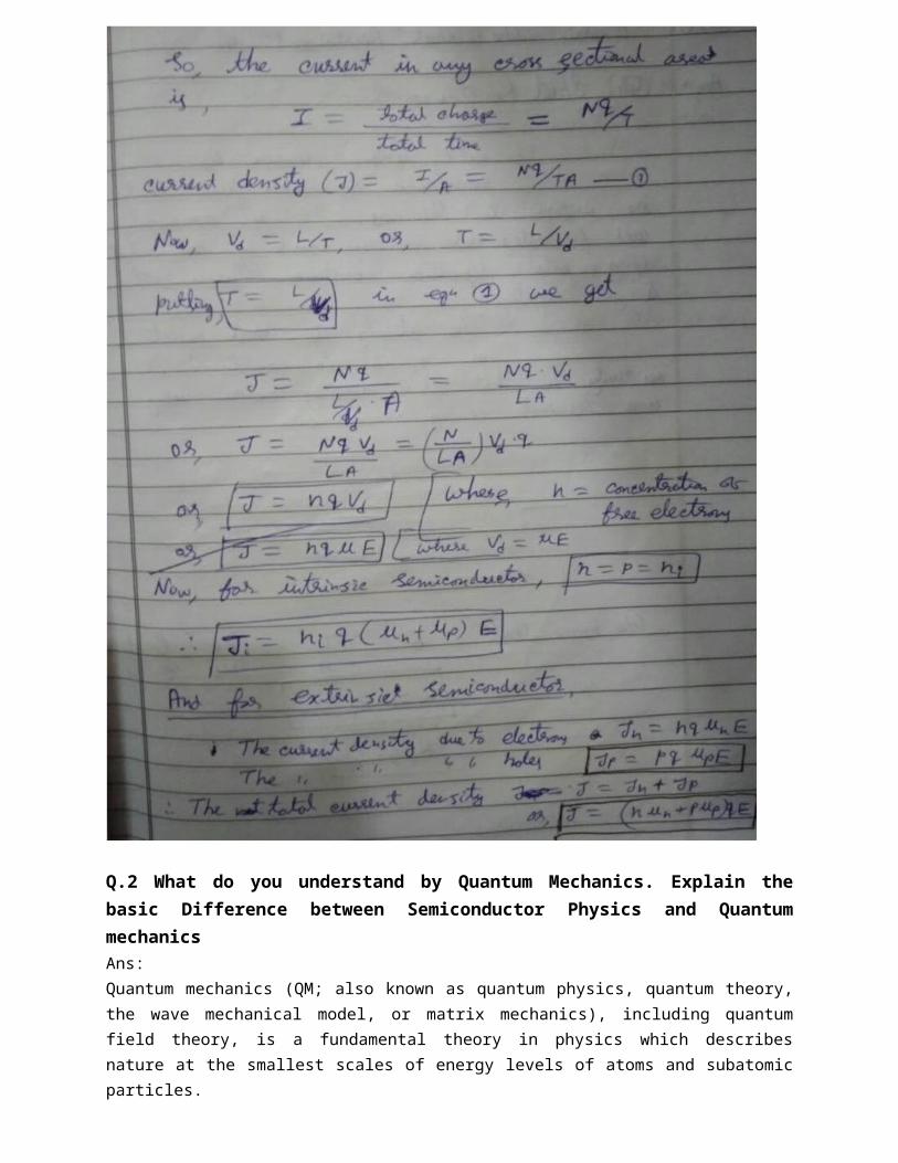
Q.1 Derive the Drift Current for Intrinsic and Extrinsic Semiconductor.Ans:

Q.2 What do you understand by Quantum Mechanics. Explain the basic Difference between Semiconductor Physics and Quantum mechanicsAns:Quantum mechanics (QM; also known as quantum physics, quantum theory, the wave mechanical model, or matrix mechanics), including quantum field theory, is a fundamental theory in physics which describes nature at the smallest scales of energy levels of atoms and subatomic particles.
Classical physics, the physics existing before quantum mechanics, describes nature at ordinary (macroscopic) scale. Most theories in classical physics can be derived from quantum mechanics as an approximation valid at large (macroscopic) scale. Quantum mechanics differs from classical physics in that energy, momentum, angular momentum and other quantities of a system are restricted to discrete

values (quantization); objects have characteristics of both particles and waves (wave-particle duality); and there are limits to the precision with which quantities can be measured (uncertainty principle).
Quantum mechanics gradually arose from theories to explain observations which could not be reconciled with classical physics, such as Max Planck's solution in 1900 to the black-body radiation problem, and from the correspondence between energy and frequency in Albert Einstein's 1905 paper which explained the photoelectric effect. Early quantum theory was profoundly re-conceived in the mid-1920s by Erwin Schrödinger, Werner Heisenberg, Max Born and others. The modern theory is formulated in various specially developed mathematical formalisms. In one of them, a mathematical function, the wave function, provides information about the probability amplitude of position, momentum, and other physical properties of a particle.
Important applications of quantum theory include quantum chemistry, quantum optics, quantum computing, superconducting magnets, light-emitting diodes, and the laser, the transistor and semiconductors such as the microprocessor, medical and research imaging such as magnetic resonance imaging and electron microscopy. Explanations for many biological and physical phenomena are rooted in the nature of the chemical bond, most notably the macro-molecule DNA.Quantum mechanics (QM) is important because it plays a fundamental role in explaining how the world works. Physicists often say QM governs the behaviour of microscopic systems when in fact it governs the behaviour of all physical systems, regardless of their size.QM tells us a lot about the structure of reality. For example, all physical systems exist in multiple versions. Information flows between different systems and under the circumstances we are familiar with in everyday life, the different versions sort themselves into approximately autonomous layers, each of which acts approximately like the world described by classical physics. The whole of physical reality in this context is called the multiverse. And information can flow in the multiverse in ways that can’t happen in classical physics, such as single particle interference and entanglement.QM has some importance in technology as it is needed to design optical and electronic components, which often take advantage of distinctively quantum mechanical effects.QM is also important for the theory of computation. According to QM it is possible to build a universal quantum computer that can simulate any physical system. This means we can test theories about physical systems by simulating them and then checking the results of the simulations against reality.For more on quantum mechanics, you might want to read “The Fabric of Reality” and “The Beginning of Infinity” by David Deutsch.
Q.3 Explain the EBERS moll model of the Transistor.Ans: