#ˇ ˛ˇ˘ ˙ ?˘ - keekleskeekles.org/~w9cr/tait 2020 software and docs/t2000_servicemanual... ·...
TRANSCRIPT
673)
; #?
The T2000-80 line interface kit enables connection of the T2000 receiver and transmitteraudio circuitry to a two wire transmission line. The line interface PCB is mounted in theoptions position inside the T2000 Series II radio, and is application configurable usingPCB links.
The following topics are covered in this Section:
Section Title Page
8.14.1 Components Required 8.14.2
8.14.2 Fitting 8.14.2
8.14.3 Line Interface Options 8.14.4
8.14.4 T2000-80 Set-Up 8.14.7
8.14.5 Signal Specifications 8.14.9
8.14.6 Applications 8.14.10
8.14.7 Specifications 8.14.16
8.14.8 Circuit Description 8.14.18
8.14.9 PCB Information 8.14.21

673)
!)6(
The T2000-80 kit contains the following components:
.&
1 Refer to Figure 8.14.1.
Remove the top cover of the radio by unscrewing the four cover screws, unclip theD-range blanking plate in the rear of the T2000 radio, unscrew the logic PCB andfold-out.
Position the T2000-80 PCB as shown, and connect the Micromatch connectors P13and P14 to S13 and S14 on the T2000 logic PCB.
' , 8 & * -! (.
2 T2010 & T2015: Remove R513 (0Ω resistor) on the logic PCB.
Quantity Description
1 T2000-80 Line Interface PCB assembly
1 15-way high density D-range plug
1 shroud (alternative shroud - not required for T2000 Series II radios)
28 0Ωchip resistors
1 1µ capacitor (*C64)
1 4µ7 capacitor (*C60)
3 M3x8 pan Pozi Taptite screws
2 4-40x¼ pan Pozi Taptite screws (black)
T2000-80 PCB
S24
S21
CGND
BC
D1
BC
D0
TP609
T2010 & T2015Logic PCB
S1
S2
S13
P13 P14
S14 S15
SK505
P2
P1

673)
3 Tx/Rx Out Function
Connect a wire from S24 on the T2000-80 PCB to S609 on the logic PCB, as shownin Figure 8.14.1.
4 External Channel Control (T2010 Only)
Connect the 2 BCD lines a shown in Figure 8.14.1.
5 Refer to Section 8.14.3, “Line Interface Options”, Section 8.14.6, “Applications”and the circuit diagram before selecting the T2000-80 PCB linking options.
Set up the T2000-80, as described in Section 8.14.4, “T2000-80 Set-Up”.
6 Carefully fold the logic and T2000-80 PCBs back in position, guiding the D-rangeconnector through the hole provided in the T2000 chassis.
Secure using the three logic PCB retaining screws and the three M3x8 screws pro-vided, and refit the top cover.
Plug the D-range assembly provided in the kit into the D-range connector (S21).
Holes are provided in the T2000 chassis for the D-range plug locking screws.Use the two black 4-40 Taptite screws provided in the kit to form the threads.
673)
#
; #8
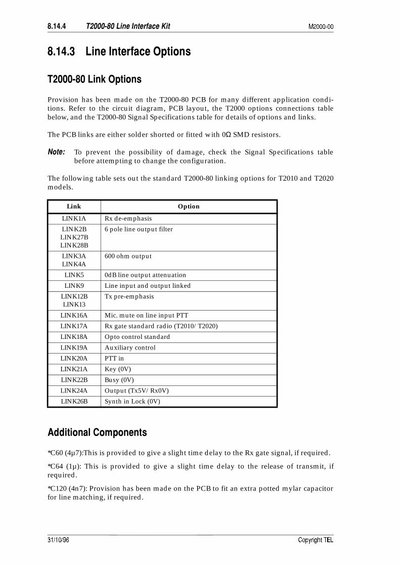
Provision has been made on the T2000-80 PCB for many different application condi-tions. Refer to the circuit diagram, PCB layout, the T2000 options connections tablebelow, and the T2000-80 Signal Specifications table for details of options and links.
The PCB links are either solder shorted or fitted with 0Ω SMD resistors.
To prevent the possibility of damage, check the Signal Specifications tablebefore attempting to change the configuration.
The following table sets out the standard T2000-80 linking options for T2010 and T2020models.
((!
*C60 (4µ7):This is provided to give a slight time delay to the Rx gate signal, if required.
*C64 (1µ): This is provided to give a slight time delay to the release of transmit, ifrequired.
*C120 (4n7): Provision has been made on the PCB to fit an extra potted mylar capacitorfor line matching, if required.
Link Option
LINK1A Rx de-emphasis
LINK2BLINK27BLINK28B
6 pole line output filter
LINK3ALINK4A
600 ohm output
LINK5 0dB line output attenuation
LINK9 Line input and output linked
LINK12BLINK13
Tx pre-emphasis
LINK16A Mic. mute on line input PTT
LINK17A Rx gate standard radio (T2010/T2020)
LINK18A Opto control standard
LINK19A Auxiliary control
LINK20A PTT in
LINK21A Key (0V)
LINK22B Busy (0V)
LINK24A Output (Tx5V/Rx0V)
LINK26B Synth in Lock (0V)

673)
; (!
The following table describes the T2000-80 pad connections found on the bottom side ofthe T2000-80 PCB.
Pad Signal Description
S22 BCD1 Connect to S15 pins 9 (BCD0) and 10 (BCD1) on T2010 logic PCB for channel remote switching. Enabled in software.S23 BCD0
S24 TX-REG Output indicating whether the radio is transmitting or receiving. Used for modem control applications.Tx = +5VRx = 0V
S25 Spare Uncommitted line to S21
S35 CGND True ground used for RF decoupling capacitors. Must be connected to radio chassis if logic and T2000-80 PCBs are folded out during set-up and test.

* 673)
!
The following table described the signals used for line interface on P13 and P14.
Pin No.
Signal Description
P13-1 DET-AF-OUT Output, buffered and low pass filtered, for flat response (60% devia-tion, 0.25Vp-p, 1kHz).
P13-3 RX-LINE-OUT De-emphasised and high pass filtered output (60% deviation, 0.4Vp-p, 1kHz). High pass filter circuit depends on presence of sub-audible tone signalling. Used for de-emphasised response.
P13-6 TX-LINE-IN Input to pre-emphasis stage, bypasses compressor. Used for the pre-emphasised response (60% deviation, 0.3Vp-p, 1kHz). Line input will override microphone signal if both are present.
P13-8 TX-SIG-IN Low gain input to T2000 limiter stage. Bypasses pre-emphasis and high pass filtering, used for the flat response (60% deviation, 2.2Vp-p, 1kHz).
P13-11 OPT-GND Earth from the regulator section of the T2000 main PCB. Used to avoid earth loop noise.
P13-12 +13.8V-UNSW Unswitched +13.8V supply from the T2000. Powers audio PA and external opto key circuits.
P14-1 +13.8V Switched +13.8V supply from T2000. Powers line interface PCB +8V regulator.
P14-2 +5.0V +5V from T2000 main PCB regulator. Powers hex invertor ICs and trunking switches.
P14-3 BUSY Output BUSY = 0V is used to inhibit line input derived key and line input mutes. On trunked versions is used for inhibit logic.
P14-4 RX-GATE Output port used to open the mute element in the T2000. Used to control line output mute.Note: Unmute = +5V for T2010 and T2020;Unmute = 0V for T2030 and T2040.This also drives the line key and opto driver indirectly.
P14-5 PTT-TO-OPT Output mirrors PTT from microphone or signalling. PTT = 0V. On trunked versions is used for inhibit logic.
P14-6 PTT-FROM-OPT Input port to key transmitter. Used for line input derived key and microphone derived key.
P14-7 IN-LOCK Synthesiser phase lock detector output. Used for modem control applications. Lock = 0V.
P14-8 MIC-MUTE Input port used to disable local microphone signal on line input derived PTT (not on microphone PTT). Mute = +5V.
P14-13 AUX Auxiliary control output configurable in software. Used to enable/disable crossband linking, 2 wire linking etc. (see trunked versions). Aux on = +5V.
Trunking Models: Additional Functions
P14-5 PTT-TP-OPT For inhibiting modem output on PTT from microphone.
P14-10 EMERG Performs a new function. ‘External call request’ = 0V input. Used for modem calls on a trunked system.
P14-11 CALL-SW Performs a new function. ‘Traffic channel allocated’ = +5V output. Used for modem calls on trunked system.
P14-13 FCN/BELL/AUX Performs a new function. ‘Not clear to send’ = +5V output. Used for modem calls on trunked system.

673) +
; ;4
56)6(
• AF signal generator
• distortion analyser
• frequency counter
• Modulation analyser
• High impedance voltmeter (e.g. VTVM)
• Oscilloscope
• Power meter
• Power supply (+13.8V)
• RF signal generator
• 40dB RF attenuator
• 600Ω step attenuator
The following diagram shows the test set-up.
' 12 $3
RF RF
4ΩSpeaker
Line
In/O
ut
600Ω
Pwr/Spkr
Option Board
Control Board
RF
OPT
S21-12Busy/Rx Gate Out1K
5V Logic
S20-10 Gnd
DC Control
S21-1 Opto In
Opto In
S21-4 +13.8V Out
S21-3 +8V Out
Opto Key
S21-2 Opto Out
FrequencyCounter
AFSignalGenerator
Ext. AF
RF SignalGenerator
RF ModulationAnalyser
AF
+13.8VPowerSupply
40dBPad
PowerMeter
DummyMic. &PTT
AudioVoltmeter
AudioVoltmeter
DistortionMeter
AFSignalGenerator
Oscilloscope
FrequencyCounter
T2000
MainBoard
Test Signal
600ΩStep Attenuator
Mic. Socket
Test Signal(Speech)
TestMic. &PTT
S20-11 PTT In
673)
;4
1 The adjustment section assumes that the T2000 radio has been correctly alignedfor normal operation. Refer to Section 8.14.3, “Line Interface Options” and the cir-cuit diagram for linking and application details.
2 If the logic and T2000-80 PCBs are unscrewed and folded out for adjustment, awire should be temporarily fitted from the radio chassis to the options chassisground pad (S35), as shown in Figure 8.14.1.
3 Signals for balanced transmissions are generally less than 0dBm, and are typicallybetween -10dBm and -20dBm.
4 Ensure that the LED is on ( LED on trunking radios).
Deviation settings are given first for wide band radios, followed by settings fornarrow band radios in brackets [ ].
##,
1 Ensure that the LED is on ( LED on trunked radios).
2 Monitor the line output (S21 pin 5).
Apply an on channel signal from the RF signal generator at an output level of-70dBm, modulated to ±3kHz [±1.5kHz] deviation, at 1kHz AF.
Adjust the RV1 (line output control) for the required output level.
If the line output level is to be less than -15dBm, short LINK6 (600Ω output) andremove LINK5, to select 15dB of attenuation.
#,
1 Monitor the line input (S21 pin 15).
Ensure the indicator is off, and key the transmitter via the opto input (+8V).
2 Adjust RV2 (line input sensitivity control) until ±3kHz [±1.5kHz] deviation at1kHz is achieved.
For input signals of greater than -15dBm, set the line input attenuation for 15dB(LINK11 open).
7!
This circuit delays audio gate turn on after PTT, to prevent squelch noise bursts inrepeater applications.
1 Enable the time delay circuit by solder shorting LINK23.
2 Set the required time delay using RV3 (time delay control).
Fn
Fn
673) -
&
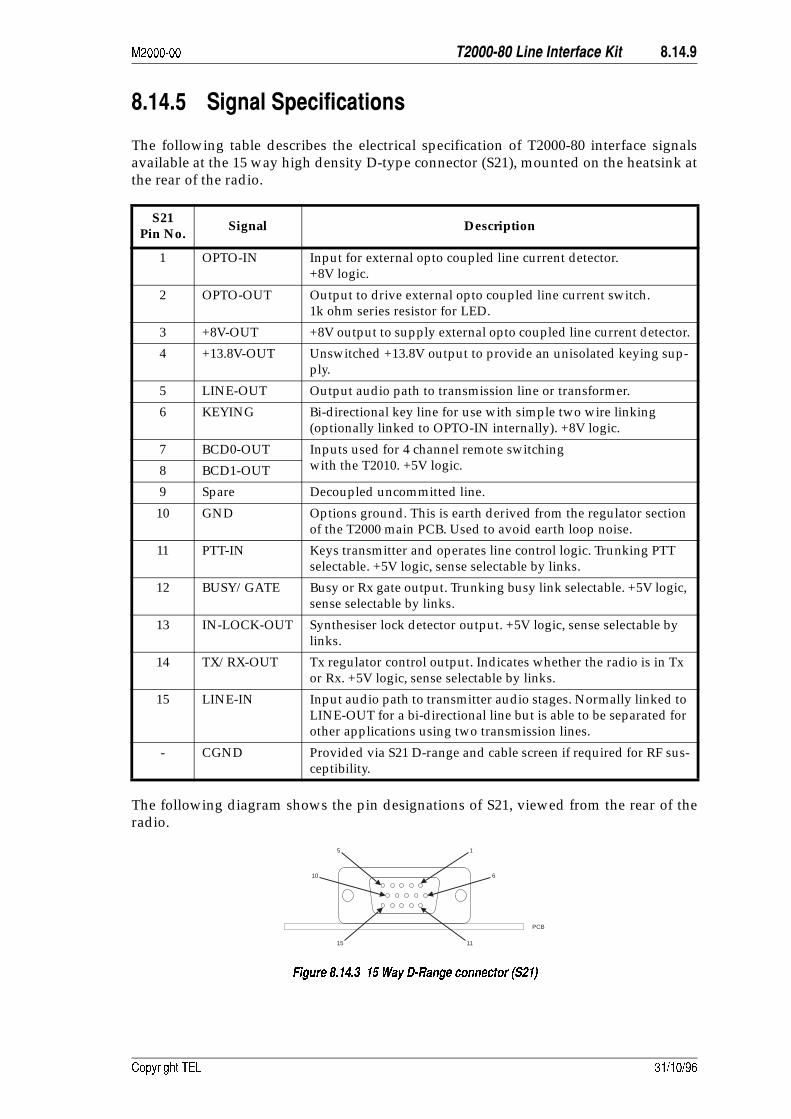
The following table describes the electrical specification of T2000-80 interface signalsavailable at the 15 way high density D-type connector (S21), mounted on the heatsink atthe rear of the radio.
The following diagram shows the pin designations of S21, viewed from the rear of theradio.
' 56 -$.
S21Pin No.
Signal Description
1 OPTO-IN Input for external opto coupled line current detector.+8V logic.
2 OPTO-OUT Output to drive external opto coupled line current switch.1k ohm series resistor for LED.
3 +8V-OUT +8V output to supply external opto coupled line current detector.
4 +13.8V-OUT Unswitched +13.8V output to provide an unisolated keying sup-ply.
5 LINE-OUT Output audio path to transmission line or transformer.
6 KEYING Bi-directional key line for use with simple two wire linking (optionally linked to OPTO-IN internally). +8V logic.
7 BCD0-OUT Inputs used for 4 channel remote switchingwith the T2010. +5V logic.8 BCD1-OUT
9 Spare Decoupled uncommitted line.
10 GND Options ground. This is earth derived from the regulator section of the T2000 main PCB. Used to avoid earth loop noise.
11 PTT-IN Keys transmitter and operates line control logic. Trunking PTT selectable. +5V logic, sense selectable by links.
12 BUSY/GATE Busy or Rx gate output. Trunking busy link selectable. +5V logic, sense selectable by links.
13 IN-LOCK-OUT Synthesiser lock detector output. +5V logic, sense selectable by links.
14 TX/RX-OUT Tx regulator control output. Indicates whether the radio is in Tx or Rx. +5V logic, sense selectable by links.
15 LINE-IN Input audio path to transmitter audio stages. Normally linked to LINE-OUT for a bi-directional line but is able to be separated for other applications using two transmission lines.
- CGND Provided via S21 D-range and cable screen if required for RF sus-ceptibility.
5 1
10 6
1115
PCB

673)
*
.
The frequency response of the line output low pass filter is selectable by LINK2, LINK27and LINK28.
• 2 pole: -12dB/octave stopband attenuation, f > 4kHz.
• 6 pole: -36dB/octave stopband attenuation, f > 4kHz.
The 2 pole LPF is for applications requiring minimal group delay and stopband attenua-tion, e.g. standard configuration, crossband 2 wire + earth, modem connection.
The 6 pole LPF is for applications requiring external network connection where stop-band attenuation is mandatory above 4kHz, e.g. crossband via external network (bal-anced line + opto key), remote controlled audio via external network (balanced line +opto key).

673)
9#8&
This is the control of 2 radios operated together, crossband or repeater linked.
1 Check that LINE-OUT is linked toLINE-IN internally (LINK9 fitted).
Fit LINK15 to link KEYING toOPTO-IN. This provides control inboth directions. The unit generat-ing the keying signal is already Txinhibited.
2 Wire LINE-OUT (S21-5) on oneT2000 to LINE-OUT (S21-5) on theother T2000. Wire KEYING (S21-6)on one T2000 to KEYING (S21-6)on the other T2000.
T2000No. 1
-+Power Suppply13.8V
4ΩSpeaker
Pwr/Spr
T2000No. 2
-+
PowerSuppply13.8V
4ΩSpeaker
Pwr/SprHDD-Range
HDD-Range
Line Out to Line Out
Keying I/O to Keying I/O
3 The time delay circuit may be required to eliminate squelch noise bursts for cross-band operation with repeaters. LINK23 enables this circuit, which is adjustableusing RV3 (refer to Section 8.14.4, “T2000-80 Set-Up”).
The 2 wire circuit assumes that the 2 radios are effectively earthed together ateither the power supply or the power connector.
A high line level is desirable to avoid earth noise i.e. 0dBm (0.775Vrms).
!3()(
Crossbanded radios i.e. UHF/VHF, can be achieved by using space isolated antennas toavoid de-sensing, as shown below.
Alternatively, in-band linked radios will require a duplexor to feed a common aerial.
T2000No. 1
T2000No. 2
-+ -+Power Suppply13.8V
Power Suppply13.8V
4ΩSpeaker
4ΩSpeaker
Pwr/Spr Pwr/Spr
Duplexor
Common Antenna UHF AntennaVHF Antenna
RF RF
673)
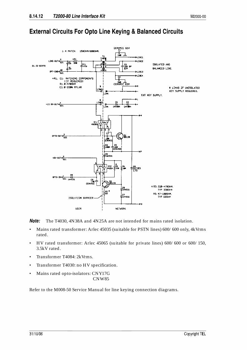
5=!.#?&</(!
The T4030, 4N38A and 4N25A are not intended for mains rated isolation.
• Mains rated transformer: Arlec 45035 (suitable for PSTN lines) 600/600 only, 4kVrmsrated.
• HV rated transformer: Arlec 45065 (suitable for private lines) 600/600 or 600/150,3.5kV rated.
• Transformer T4084: 2kVrms.
• Transformer T4030: no HV specification.
• Mains rated opto-isolators: CNY17GCNW85
Refer to the M008-50 Service Manual for line keying connection diagrams.
673)
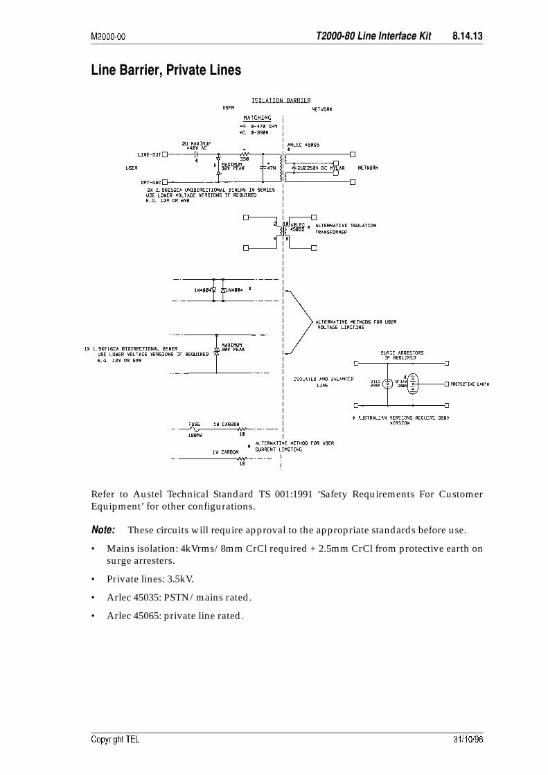
#/A,#
Refer to Austel Technical Standard TS 001:1991 ‘Safety Requirements For CustomerEquipment’ for other configurations.
These circuits will require approval to the appropriate standards before use.
• Mains isolation: 4kVrms/8mm CrCl required + 2.5mm CrCl from protective earth onsurge arresters.
• Private lines: 3.5kV.
• Arlec 45035: PSTN/mains rated.
• Arlec 45065: private line rated.

673)
"
' 89 )
Cores must be properly aligned when assembled.Core faces must be clean and free from grease and dirt.Ensure tag plate is firmly pressed against can before folding tabs.
Core .. P26/16 - µ1910
Former .. single
Number of Turns:Primary .. 250 bifilarSecondary .. 250 bifilar
Material .. 15mm self flux
Tape .. thermosetting electrical grade
Sleeving .. inside diameter all colours, 0.5mm
Inductance 1 .. 6±1.5H(total series inductance, pin 1 to 5 - connect pins 2 & 3, 4 & 8 and 7 & 6)
Inductance 2 .. 1.5±0.4H(any winding, with all others open circuit)
Secondary
Primary
56 7
8
43 2
1
Underside View
Can
Core
Former(Wound)
Tag plate
Spring
MylarInsulator
Section A-A
Primary
Secondary
Leads tobe sleeved
Tin endsof leads
Tape outsideof turns
Former and Windings
1
3
2
4
SleevingColours
SleevingColours
Start
PriBifilar
Finish Finish
Pri 250T - 15 Red & GreenSec 250T - 15Red & Green
Green250T
Green250T
Red250T
Red250T
8
6
7
5
Brown
BlueRed
A A
Start
SecBifilar
Grey
Sleeving Colours:Pin 1,3 Brown 2,4 Red
5,7 Blue 6,8 Grey
673)
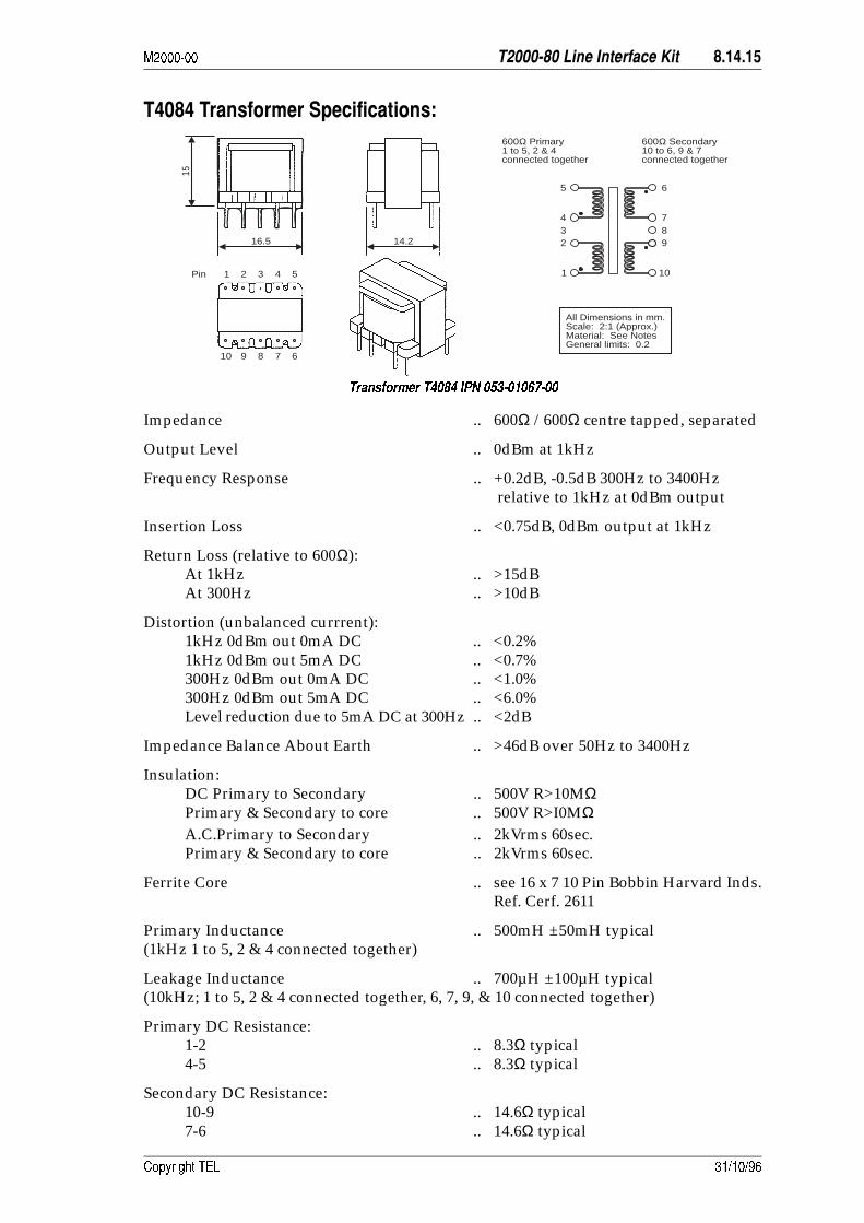
"
'' 89 ")
Impedance .. 600Ω /600Ω centre tapped, separated
Output Level .. 0dBm at 1kHz
Frequency Response .. +0.2dB, -0.5dB 300Hz to 3400Hz relative to 1kHz at 0dBm output
Insertion Loss .. <0.75dB, 0dBm output at 1kHz
Return Loss (relative to 600Ω):At 1kHz .. >15dBAt 300Hz .. >10dB
Distortion (unbalanced currrent):1kHz 0dBm out 0mA DC .. <0.2%1kHz 0dBm out 5mA DC .. <0.7%300Hz 0dBm out 0mA DC .. <1.0%300Hz 0dBm out 5mA DC .. <6.0%Level reduction due to 5mA DC at 300Hz .. <2dB
Impedance Balance About Earth .. >46dB over 50Hz to 3400Hz
Insulation:DC Primary to Secondary .. 500V R>10MΩ
Primary & Secondary to core .. 500V R>I0MΩA.C.Primary to Secondary .. 2kVrms 60sec.
Primary & Secondary to core .. 2kVrms 60sec.
Ferrite Core .. see 16 x 7 10 Pin Bobbin Harvard Inds.Ref. Cerf. 2611
Primary Inductance .. 500mH ±50mH typical(1kHz 1 to 5, 2 & 4 connected together)
Leakage Inductance .. 700µH ±100µH typical(10kHz; 1 to 5, 2 & 4 connected together, 6, 7, 9, & 10 connected together)
Primary DC Resistance:1-2 .. 8.3Ω typical4-5 .. 8.3Ω typical
Secondary DC Resistance: 10-9 .. 14.6Ω typical7-6 .. 14.6Ω typical
600Ω Secondary10 to 6, 9 & 7connected together
600Ω Primary1 to 5, 2 & 4connected together
6
789
10
5
432
1
All Dimensions in mm.Scale: 2:1 (Approx.)Material: See NotesGeneral limits: 0.2
15
16.5 14.2
678910
Pin 1 2 3 4 5

* 673)
+
;
Input Voltage .. 10.8V to 16V DC(from S13 & S14 on the T2000 logic PCB)
Operating Temperature Range .. -10°C to +60°C ambient
DC Input Current .. < 40mA total (+13.8V supply)
Line Input Sensitivity (60% deviation) .. -20dBm to +6dBm (600Ω)
Line Output Level (60% deviation) .. -20dBm to +6dBm (600Ω)
Line Impedance .. 600 or 150Ω
Return Loss (300Hz to 3kHz). .. > 20dB relative to 600 or 150Ω
Line Output Filter Response (stopband):2 pole .. -12dB/octave, f > 4kHz6 pole .. -36dB/octave, f > 4kHz
B ; #
a Receiver + Line Output
Receiver Frequency Response (relative to 1kHz, 60% deviation):Receiver Processed:
Bandwidth .. 300Hz to 3kHz (standard) 400Hz to 3kHz (CTCSS)
Response .. +1, -3dB relative to -6dB/octaveReceiver Unprocessed .. +1, -3dB (300Hz to 3kHz)
Test signal .. -70dBm RF, 60% deviation at 1kHz,0dBm line output.
Signal-to-Noise Ratio:Narrow Band .. > 39dBWide Band .. > 45dB
Mute Ratio .. > 65dB
Distortion (30kHz band width distortion meter):Wide Band De-emphasised .. < 2%Narrow Band De-emphasised .. < 3%Wide Band Flat .. < 4%Narrow Band Flat .. < 6%
673) +
b Transmitter + Line Input
Transmitter Frequency response:Transmitter Processed:(relative to 1kHz, 20% deviation, below limiting)
Bandwidth .. 300Hz to 2.55kHz (narrow band) 300Hz to 3kHz (wide band)
Response .. +1, -3dB relative to +6dB/octaveTransmitter Unprocessed (relative to 1kHz, 60% deviation):
Bandwidth .. 300Hz to 2.55kHz (narrow band) 300Hz to 3kHz (wide band)
Response .. +1, -3dB
Test signal .. 0dBm line input, 1kHz, 60% deviation
Signal-to-Noise Ratio:(demodulated, filtered 300Hz to 3kHz + de-emphasised 750µsrms)
Narrow Band .. > 39dBWide Band .. > 45dB
Distortion .. < 2%(demodulated, filtered 15kHz low pass)

673)
!7
Refer to Figure 8.14.4, Figure 8.14.4 and the circuit diagram.
#$
Flat or de-emphasised audio from the receiver is selected by links to DET-AF-OUT orRX- LINE-OUT. Receiver audio passes through a mute element to a buffer amplifier, andthen to three stages of low pass filtering. Two responses are selectable by links: 2 pole or6 pole roll-off beyond 4kHz.
The filtered signal passes to a second mute element and level control before passing tothe line output drive amplifier. Line output impedance and attenuation are selectable bylinks. Line output can be linked to line input for a shared line in, line out.
'' , 8 & &: 5
#$
The line input has terminations for two line impedances which are link selectable. Theline input level can be attenuated, if required, before passing to the line sensitivity con-trol. Protection diodes are fitted to prevent the following amplifier stage from beingoverdriven.
The amplifier provides gain and buffers the signal, which is split into two paths foreither pre-emphasis or flat response. The pre-emphasis path is via a mute element andoptions linking. This signal drives TX-LINE-IN, which will override the microphonesignal. Normally, the microphone is muted on line derived PTT.
The flat response path is amplified and then passes to a mute element which drivesTX-SIG-IN. This input requires a high signal level, due to the high input impedance.The amplifier is disabled by links, when not used, to prevent the possibility of crosstalkand leakage to other circuitry.
Control Logic
ExternalLogic
T2000Logic
PowerSuppliers
LineDriver Attenuator
Attenuator
MuteElement
MuteElement
MuteElement
MuteElement
Line OutLevelLink2
B AN=4N=2
GainStage
BufferAmp
LineSensitivity
Line Out
Line In
T2000Control PCBVia OptionConnectors
RxAFDe-Emph.
RxAFFlat
TxAFPre-Emph.
TxAFFlat
External CircuitsVia HD D-Range
Connector
673) -
!#&
For standard mobiles in normal operation, the audio mute elements, transmit inhibitand opto driver are all inhibited by the auxiliary control. The radio can be used nor-mally with ‘auxiliary off’, and line controlled with ‘auxiliary on’.
With ‘auxiliary on’, the line output mute elements and opto driver are controlled fromthe RX-GATE. A signal on the BUSY line inhibits the transmitter line key circuitry. Linederived key signals, such as OPTO-IN, KEYING and PTT-IN, can be used to key theradio, provided the auxiliary control is on and the radio is not busy.
The KEYING line is used for back-to-back control of two radios, each with a line inter-face PCB. This enables crossband linking to be achieved with a minimum of external cir-cuitry. In this case, the KEYING line can be linked to the OPTO-IN line on each unit,with a wire between the two OPTO-IN lines providing bi-directional control. KEYING iscontrolled by the receive gate and is used to drive the opto input of another line inter-face PCB.
The opto input is intended to be connected to the output of an optocoupler circuit (BJT)used for loop and tail keying via transmission lines (refer to Section 8.14.6, “Applica-tions”).
The opto output is intended to be connected to the input of an optocoupler circuit (LED)used for loop and tail keying via transmission lines (refer to Section 8.14.6, “Applica-tions”). The sense of this circuit can be changed by a link.
An adjustable time delay circuit is available to prevent transmitter cycling when cross-band connected radios are both operating on repeater channels. The circuit is adjustableto approximately 1.5 seconds, with the time delay control fully clockwise, and can bedisabled completely by removing a link.
PTT-IN can be used to key the transmitter. Links are available to enable either logicsense. For trunked versions using modems, a circuit is provided to set up a call automat-ically.
Control logic for telemetry and modems is provided so that the radio can be operatedautomatically. IN-LOCK-OUT, BUSY/GATE and TX/RX-OUT outputs can be set bylinks for either logic sense.
Trunked modems operate in a different manner, and first have to set up a call to obtain atraffic channel allocation.
Logic is available which requires several link changes, as some of the radio options con-nections perform different functions:
Standard Trunked
AUX on/off not clear to send
emergency external call request
call traffic channel allocated
673)
+5V is provided from the main regulator via the options connector. +8V is provided by aTO-92 3 terminal regulator. This is also available on the T2000-80 PCB D-range connec-tor, for powering an optocoupler transistor used for line key current detection. The+13.8V input of the regulator is derived from the options connector. The +3.2V rail pro-vides bias to the audio stages and is derived from the +8V regulator. The unswitched+13.8V from the options connector powers the line drive amplifier, and is available onthe T2000-80 D-range for use as an unisolated line key supply option.

; #0: ; +; 2
673)
- !/
( %
( %
" %
(
(
" %
( %
( %
( %
( %
" %
( %
( %
" %
%
(
(
(
(
(
(
(
(
(
(
(
(
(
(
(
(
(
%
%
(
%
(
(
%
%
(
( %
( %
( %
%
%
(
( %
(
(
(
(
(
(
(
(
(
( %
(
(
" %
( %
(
(
(
#$ % ( %
#$ % ( &
#$ % ( %
#$ % ( % %
#$ % ( %
#$ % ( %
#$ % ( %
#$ (
#$ %
#$ %
#$ (
#$ %
#$ % (
#$ % (
#$ & %
#$ *
! ( . % %(
(
! ( . % %(
! ( . % %(
! ( . % %(
! ( . % %(
! ( . % %(
! ( . % %(
! ( . % %(
! ( . % %(
! ( . % %(
! ( . % %(
! ( . % %(
! ( . % %(
! ( . % %(
! ( . % %(
! ( . % %(
! ( . % %(
! ( . % %(
! ( . % %(
! ( . % %(
! ( . % %(
! ( . % %(
! ( . % %(
! ( . % %(
! ( . % %(
! ( . % %(
! ( . % %(
! ( . % %(
% " % (
& " %
& " '
) #$ ! %
) #$ ! %
) #$ ! %
) #$ ! %
) #$ ! %
) #$ ! %
) #$ ! %
) #$ ! %
) #$ ! %
) #$ ! %
) #$ ! %
) #$ ! %
) #$ ! %
% 0
% 0
% 0
! (
! (
! (
! (
! (
! (
! (
! (
! (
! (
! (
! (
! (
! (
! (
673)
! (
! (
! (
! (
! (
! (
! (
! (
! (
! (
! (
! (
! (
! (
! (
! (
! (
! (
! (
! (
! (
! (
! (
! (
! (
! (
! (
! (
! (
! (
! (
! (
! (
! (
! (
! (
! (
! (
! (
! (
! (
! (
! (
! (
! (
! (
! (
! (
! (
! (
! (
! (
! (
! (
! (
! (
! (
! (
! (
! (
! (
! (
! (
! (
! (
! (
! (
! (
! (
! (
! (
! (
! (
! (
! (
! (
! (
! (
! (
! (
! (
! (
! (
! (
! (
! (
! (
! (
! (
! (
! (
! (
! (
! (
! (
! (
! (
! (
" & ( " & &
'$<' % #'$
#'$
% !!* & "
# $
& " & ( %
% " % (
(%%!% " & % % %
(%%!% " & %& (
! %.
#% ( (% $
%. .
( ! (
( ! ) !
& '
& ( &
% %
&

673)
; ()(=0: ; +; 2
3
!
3
!
3
3
3
3
3
3
3
3
"
3
*
* 3
* 3
3
3
! "
*
*
*
*
*
"
3
3
*
*
3
4
3
3
4
4 3
3
3
3
3
3
3
* 3
* 3
3
*
*
*
*
*
*
6
7
3)
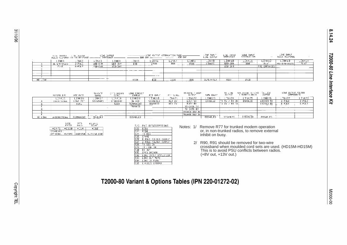
Notes: 1/ Remove R77 for trunked modem operationor, in non-trunked radios, to remove externalinhibit on busy.
2/ R90, R91 should be removed for two-wirecrossband when moulded cord sets are used. (HD15M-HD15M)This is to avoid PSU conflicts between radios.(+8V out, +13V out.)
; %<30: ; +; 2
6
7
3)
"#0(
!
$
*
673)
"#0( !!##$

&)&$)'+"!),$
!,),&)-0$#)

&)&$)'+"!),$