© r.lauwereins imec 2001 digital design combina- torial circuits sequential circuits fsmd design...
TRANSCRIPT
2/1
© R.LauwereinsImec 2001
Digitaldesign
Combina-torialcircuits
Sequentialcircuits
FSMDdesign
VHDL
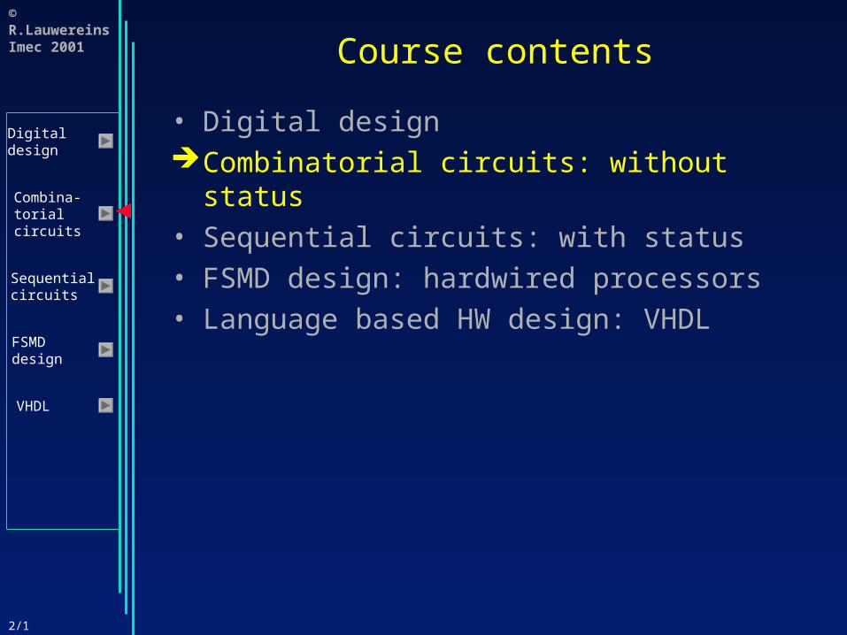
Course contents
• Digital designCombinatorial circuits: without status• Sequential circuits: with status• FSMD design: hardwired processors• Language based HW design: VHDL

2/2
© R.LauwereinsImec 2001
Digitaldesign
Combina-torialcircuits
Sequentialcircuits
FSMDdesign
VHDL
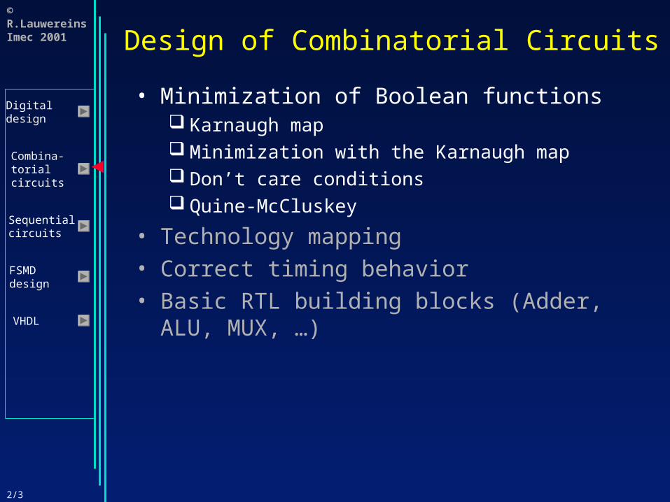
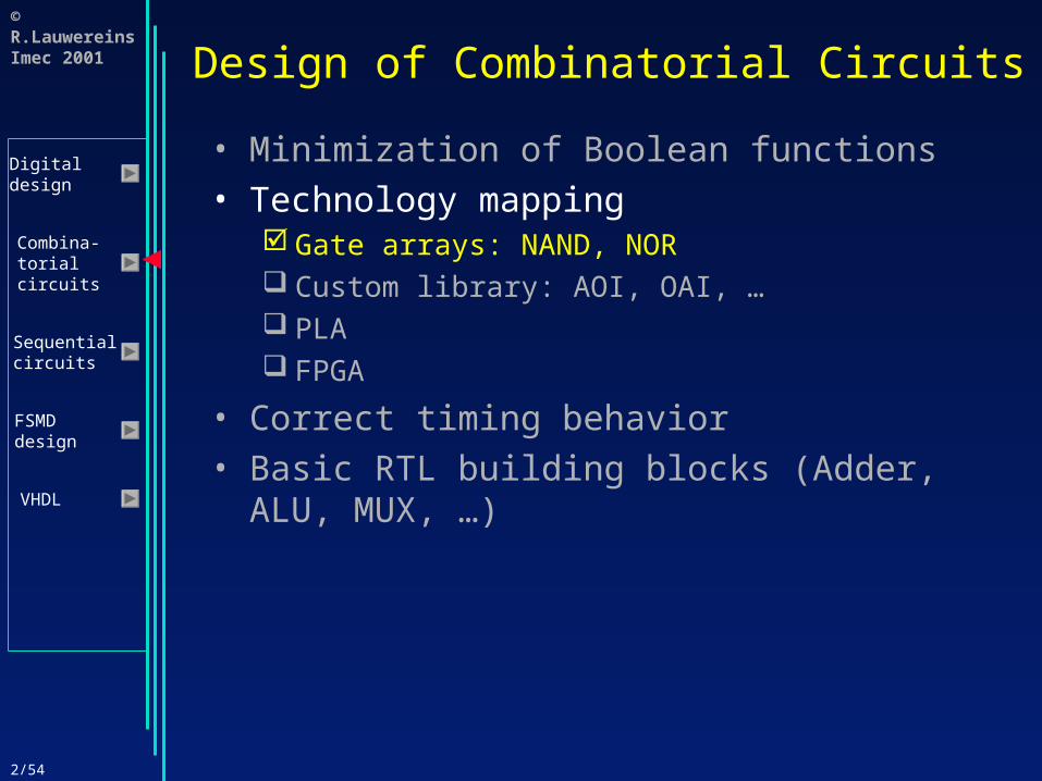
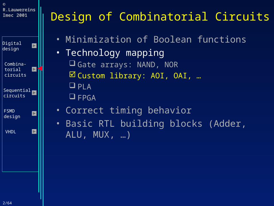
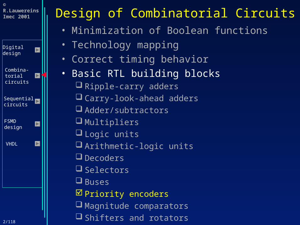
Design of Combinatorial Circuits
• Minimization of Boolean functions• Technology mapping• Correct timing behavior• Basic RTL building blocks (Adder, ALU, MUX,
…)
2/3
© R.LauwereinsImec 2001
Digitaldesign
Combina-torialcircuits
Sequentialcircuits
FSMDdesign
VHDL
Design of Combinatorial Circuits
• Minimization of Boolean functions Karnaugh map Minimization with the Karnaugh map Don’t care conditions Quine-McCluskey
• Technology mapping• Correct timing behavior• Basic RTL building blocks (Adder, ALU, MUX,
…)

2/4
© R.LauwereinsImec 2001
Digitaldesign
Combina-torialcircuits
Sequentialcircuits
FSMDdesign
VHDL
Design of Combinatorial Circuits
• Minimization of Boolean functions Karnaugh map Minimization with the Karnaugh map Don’t care conditions Quine-McCluskey
• Technology mapping• Correct timing behavior• Basic RTL building blocks (Adder, ALU, MUX,
…)
2/5
© R.LauwereinsImec 2001
Digitaldesign
Combina-torialcircuits
Sequentialcircuits
FSMDdesign
VHDL
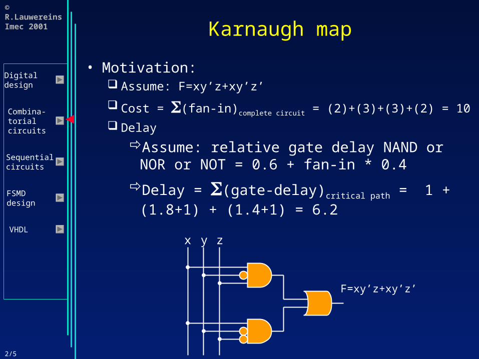
Karnaugh map
• Motivation: Assume: F=xy’z+xy’z’
Cost = (fan-in)complete circuit = (2)+(3)+(3)+(2) = 10
Delay
Assume: relative gate delay NAND or NOR or NOT = 0.6 + fan-in * 0.4
Delay = (gate-delay)critical path = 1 + (1.8+1) + (1.4+1) = 6.2
x y z
F=xy’z+xy’z’
2/6
© R.LauwereinsImec 2001
Digitaldesign
Combina-torialcircuits
Sequentialcircuits
FSMDdesign
VHDL
Karnaugh map
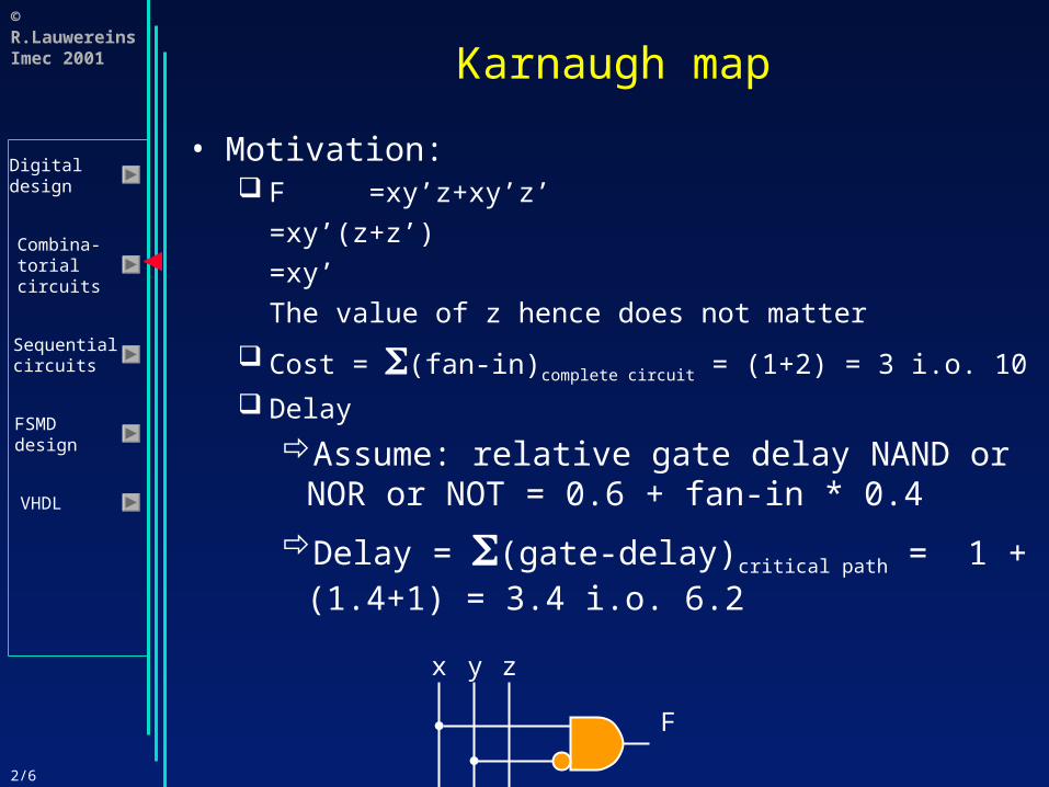
• Motivation: F =xy’z+xy’z’
=xy’(z+z’)=xy’The value of z hence does not matter
Cost = (fan-in)complete circuit = (1+2) = 3 i.o. 10
Delay
Assume: relative gate delay NAND or NOR or NOT = 0.6 + fan-in * 0.4
Delay = (gate-delay)critical path = 1 + (1.4+1) = 3.4 i.o. 6.2
x y z
F
2/7
© R.LauwereinsImec 2001
Digitaldesign
Combina-torialcircuits
Sequentialcircuits
FSMDdesign
VHDL
Karnaugh map
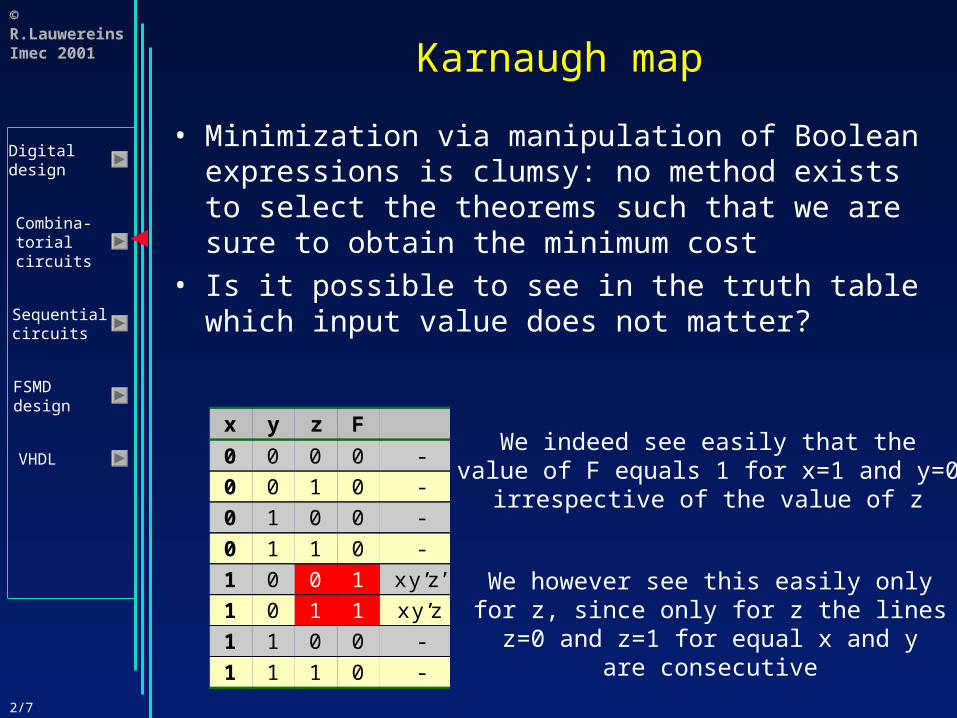
• Minimization via manipulation of Boolean expressions is clumsy: no method exists to select the theorems such that we are sure to obtain the minimum cost
• Is it possible to see in the truth table which input value does not matter?
x y z F
0 0 0 0 -0 0 1 0 -
0 1 0 0 -
0 1 1 0 -
1 0 0 1 xy’z’
1 0 1 1 xy’z
1 1 0 0 -
1 1 1 0 -
We indeed see easily that thevalue of F equals 1 for x=1 and y=0
irrespective of the value of z
We however see this easily onlyfor z, since only for z the linesz=0 and z=1 for equal x and y
are consecutive
2/8
© R.LauwereinsImec 2001
Digitaldesign
Combina-torialcircuits
Sequentialcircuits
FSMDdesign
VHDL
Karnaugh map
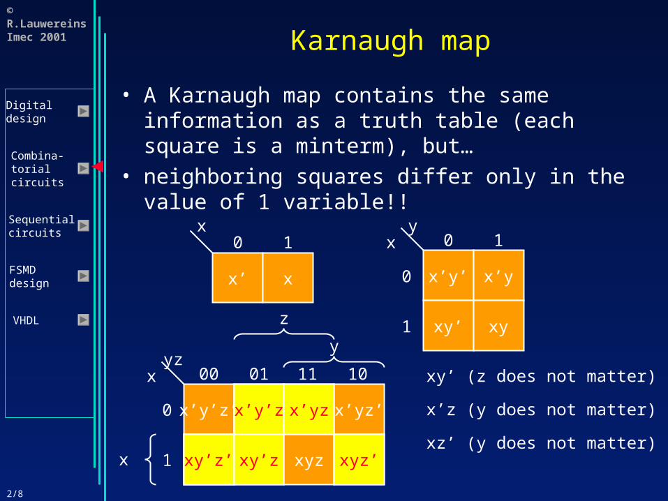
• A Karnaugh map contains the same information as a truth table (each square is a minterm), but…
• neighboring squares differ only in the value of 1 variable!!
x’ x
x0 1
x’y’ x’y
xy’ xy
x
0
1
y0 1
x’y’z’ x’y’z
xy’z’ xy’z
x
0
1
yz00 01
x’yz x’yz’
xyz xyz’
11 10
x
y
z
x’z (y does not matter)x’y’z x’yz
xy’z’ xyz’xz’ (y does not matter)
xy’z’ xy’z
xy’ (z does not matter)

2/9
© R.LauwereinsImec 2001
Digitaldesign
Combina-torialcircuits
Sequentialcircuits
FSMDdesign
VHDL
Karnaugh map
m0 m1
x0 1
m0 m1
m2 m3
x
0
1
y0 1
0 1
4 5
x
0
1
yz00 01
3 2
7 6
11 10
x
y
z

2/10
© R.LauwereinsImec 2001
Digitaldesign
Combina-torialcircuits
Sequentialcircuits
FSMDdesign
VHDL
x y z w F
0 0 0 0 10 0 0 1 0
0 0 1 0 0
0 0 1 1 0
0 1 0 0 0
0 1 0 1 1
0 1 1 0 0
0 1 1 1 1
1 0 0 0 1
1 0 0 1 0
1 0 1 0 1
1 0 1 1 0
1 1 0 0 0
1 1 0 1 1
1 1 1 0 0
1 1 1 1 1
Karnaugh map
0 1
4 5
xy
00
01
zw00 01
3 2
7 6
11 10
x
z
w
12 13
8 9
15 14
11 10
11
10
y
x y z w F
0 0 0 0 10 0 0 1 0
0 0 1 0 0
0 0 1 1 0
0 1 0 0 0
0 1 0 1 1
0 1 1 0 0
0 1 1 1 1
1 0 0 0 1
1 0 0 1 0
1 0 1 0 1
1 0 1 1 0
1 1 0 0 0
1 1 0 1 1
1 1 1 0 0
1 1 1 1 1
1
x y z w F
0 0 0 0 10 0 0 1 0
0 0 1 0 0
0 0 1 1 0
0 1 0 0 0
0 1 0 1 1
0 1 1 0 0
0 1 1 1 1
1 0 0 0 1
1 0 0 1 0
1 0 1 0 1
1 0 1 1 0
1 1 0 0 0
1 1 0 1 1
1 1 1 0 0
1 1 1 1 1
0
x y z w F
0 0 0 0 10 0 0 1 0
0 0 1 0 0
0 0 1 1 0
0 1 0 0 0
0 1 0 1 1
0 1 1 0 0
0 1 1 1 1
1 0 0 0 1
1 0 0 1 0
1 0 1 0 1
1 0 1 1 0
1 1 0 0 0
1 1 0 1 1
1 1 1 0 0
1 1 1 1 1
0
x y z w F
0 0 0 0 10 0 0 1 0
0 0 1 0 0
0 0 1 1 0
0 1 0 0 0
0 1 0 1 1
0 1 1 0 0
0 1 1 1 1
1 0 0 0 1
1 0 0 1 0
1 0 1 0 1
1 0 1 1 0
1 1 0 0 0
1 1 0 1 1
1 1 1 0 0
1 1 1 1 1
0
x y z w F
0 0 0 0 10 0 0 1 0
0 0 1 0 0
0 0 1 1 0
0 1 0 0 0
0 1 0 1 1
0 1 1 0 0
0 1 1 1 1
1 0 0 0 1
1 0 0 1 0
1 0 1 0 1
1 0 1 1 0
1 1 0 0 0
1 1 0 1 1
1 1 1 0 0
1 1 1 1 1
0 1
x y z w F
0 0 0 0 10 0 0 1 0
0 0 1 0 0
0 0 1 1 0
0 1 0 0 0
0 1 0 1 1
0 1 1 0 0
0 1 1 1 1
1 0 0 0 1
1 0 0 1 0
1 0 1 0 1
1 0 1 1 0
1 1 0 0 0
1 1 0 1 1
1 1 1 0 0
1 1 1 1 1
x y z w F
0 0 0 0 10 0 0 1 0
0 0 1 0 0
0 0 1 1 0
0 1 0 0 0
0 1 0 1 1
0 1 1 0 0
0 1 1 1 1
1 0 0 0 1
1 0 0 1 0
1 0 1 0 1
1 0 1 1 0
1 1 0 0 0
1 1 0 1 1
1 1 1 0 0
1 1 1 1 1
0
x y z w F
0 0 0 0 10 0 0 1 0
0 0 1 0 0
0 0 1 1 0
0 1 0 0 0
0 1 0 1 1
0 1 1 0 0
0 1 1 1 1
1 0 0 0 1
1 0 0 1 0
1 0 1 0 1
1 0 1 1 0
1 1 0 0 0
1 1 0 1 1
1 1 1 0 0
1 1 1 1 1
1
x y z w F
0 0 0 0 10 0 0 1 0
0 0 1 0 0
0 0 1 1 0
0 1 0 0 0
0 1 0 1 1
0 1 1 0 0
0 1 1 1 1
1 0 0 0 1
1 0 0 1 0
1 0 1 0 1
1 0 1 1 0
1 1 0 0 0
1 1 0 1 1
1 1 1 0 0
1 1 1 1 1
1
x y z w F
0 0 0 0 1
0 0 0 1 0
0 0 1 0 0
0 0 1 1 0
0 1 0 0 0
0 1 0 1 1
0 1 1 0 0
0 1 1 1 1
1 0 0 0 1
1 0 0 1 0
1 0 1 0 1
1 0 1 1 0
1 1 0 0 0
1 1 0 1 1
1 1 1 0 0
1 1 1 1 1
0
x y z w F
0 0 0 0 10 0 0 1 0
0 0 1 0 0
0 0 1 1 0
0 1 0 0 0
0 1 0 1 1
0 1 1 0 0
0 1 1 1 1
1 0 0 0 1
1 0 0 1 0
1 0 1 0 1
1 0 1 1 0
1 1 0 0 0
1 1 0 1 1
1 1 1 0 0
1 1 1 1 1
1
x y z w F
0 0 0 0 10 0 0 1 0
0 0 1 0 0
0 0 1 1 0
0 1 0 0 0
0 1 0 1 1
0 1 1 0 0
0 1 1 1 1
1 0 0 0 1
1 0 0 1 0
1 0 1 0 1
1 0 1 1 0
1 1 0 0 0
1 1 0 1 1
1 1 1 0 0
1 1 1 1 1
0
x y z w F
0 0 0 0 10 0 0 1 0
0 0 1 0 0
0 0 1 1 0
0 1 0 0 0
0 1 0 1 1
0 1 1 0 0
0 1 1 1 1
1 0 0 0 1
1 0 0 1 0
1 0 1 0 1
1 0 1 1 0
1 1 0 0 0
1 1 0 1 1
1 1 1 0 0
1 1 1 1 1
0
x y z w F
0 0 0 0 10 0 0 1 0
0 0 1 0 0
0 0 1 1 0
0 1 0 0 0
0 1 0 1 1
0 1 1 0 0
0 1 1 1 1
1 0 0 0 1
1 0 0 1 0
1 0 1 0 1
1 0 1 1 0
1 1 0 0 0
1 1 0 1 1
1 1 1 0 0
1 1 1 1 1
1
x y z w F
0 0 0 0 1
0 0 0 1 0
0 0 1 0 0
0 0 1 1 0
0 1 0 0 0
0 1 0 1 1
0 1 1 0 0
0 1 1 1 1
1 0 0 0 1
1 0 0 1 0
1 0 1 0 1
1 0 1 1 0
1 1 0 0 0
1 1 0 1 1
1 1 1 0 0
1 1 1 1 1
0
x y z w F
0 0 0 0 10 0 0 1 0
0 0 1 0 0
0 0 1 1 0
0 1 0 0 0
0 1 0 1 1
0 1 1 0 0
0 1 1 1 1
1 0 0 0 1
1 0 0 1 0
1 0 1 0 1
1 0 1 1 0
1 1 0 0 0
1 1 0 1 1
1 1 1 0 0
1 1 1 1 1
1
Fill out from truth table
2/11
© R.LauwereinsImec 2001
Digitaldesign
Combina-torialcircuits
Sequentialcircuits
FSMDdesign
VHDL
Karnaugh map
1 0
0 1
xy
00
01
zw00 01
0 0
1 0
11 10
x
z
w
0 1
1 0
1 0
0 1
11
10
y
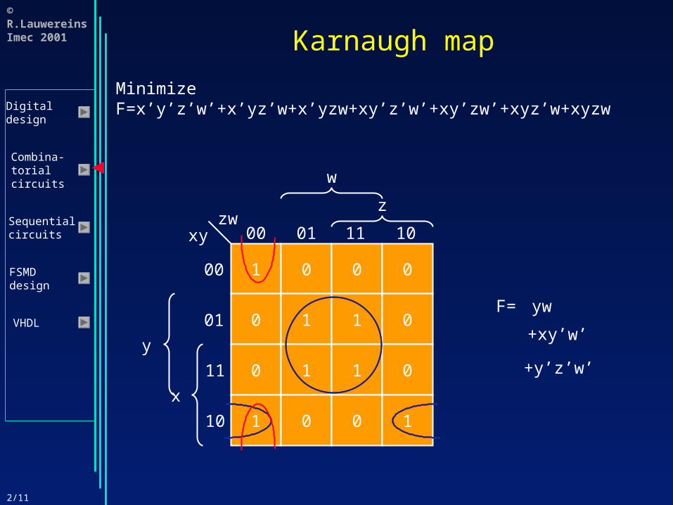
MinimizeF=x’y’z’w’+x’yz’w+x’yzw+xy’z’w’+xy’zw’+xyz’w+xyzw
F= yw
+xy’w’
+y’z’w’
2/12
© R.LauwereinsImec 2001
Digitaldesign
Combina-torialcircuits
Sequentialcircuits
FSMDdesign
VHDL
Karnaugh map
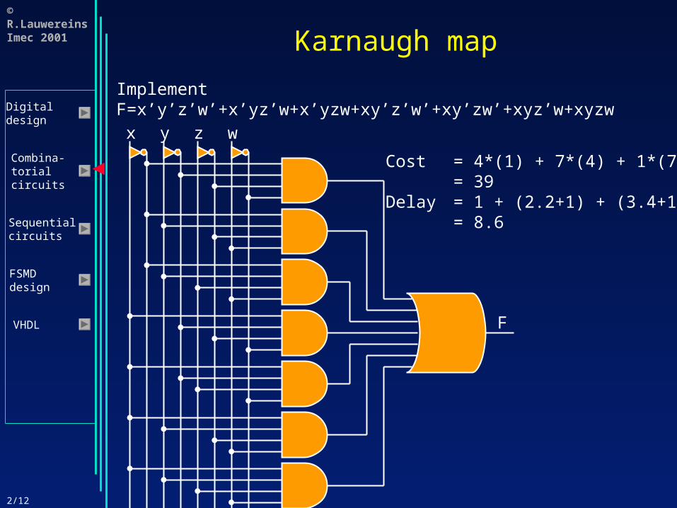
ImplementF=x’y’z’w’+x’yz’w+x’yzw+xy’z’w’+xy’zw’+xyz’w+xyzwx y z w
F
Cost = 4*(1) + 7*(4) + 1*(7)= 39
Delay = 1 + (2.2+1) + (3.4+1)= 8.6

2/13
© R.LauwereinsImec 2001
Digitaldesign
Combina-torialcircuits
Sequentialcircuits
FSMDdesign
VHDL
Karnaugh map
ImplementF=yw+xy’w’+y’z’w’x y z w
Cost = 3*(1) + {1*(2)+2*(3)} + 1*(3)= 14 i.p.v. 39
Delay = 1 + (1.8+1) + (1.8+1)= 6.6 i.p.v. 8.6
F
2/14
© R.LauwereinsImec 2001
Digitaldesign
Combina-torialcircuits
Sequentialcircuits
FSMDdesign
VHDL
Karnaugh map
0xy00
01
zw00 01 11 10
1 3 2
4 5 7 6
12 13 15 14
8 9 11 10
18 19 17 16
22 23 21 20
30 31 29 28
26 27 25 24
xy
11
10
10 11 01 00
00
01
11
10x
y
z
w
x
z
w
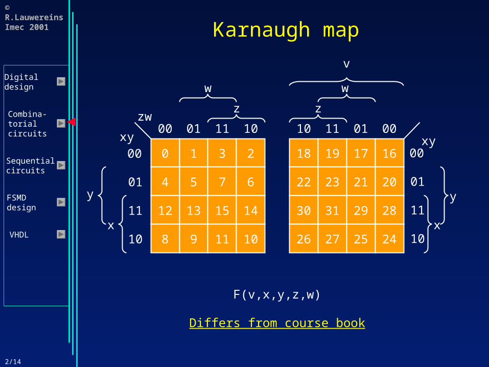
v
y
Differs from course book
F(v,x,y,z,w)
2/15
© R.LauwereinsImec 2001
Digitaldesign
Combina-torialcircuits
Sequentialcircuits
FSMDdesign
VHDL
Karnaugh map
0xy00
01
zw00 01 11 10
1 3 2
4 5 7 6
12 13 15 14
8 9 11 10
18 19 17 16
22 23 21 20
30 31 29 28
26 27 25 24
xy
11
10
10 11 01 00
00
01
11
10x
y
z
w
x
z
w
v
y
40 41 43 42
44 45 47 46
36 37 39 38
32 33 35 34
58 59 57 56
62 63 61 60
54 55 53 52
50 51 49 48
10
11
01
00
x
y
10
11
01
00
x
y u
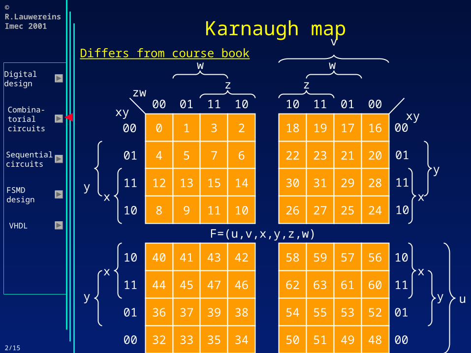
F=(u,v,x,y,z,w)
Differs from course book

2/16
© R.LauwereinsImec 2001
Digitaldesign
Combina-torialcircuits
Sequentialcircuits
FSMDdesign
VHDL
Design of Combinatorial Circuits
• Minimization of Boolean functions Karnaugh map Minimization with the Karnaugh map Don’t care conditions Quine-McCluskey
• Technology mapping• Correct timing behavior• Basic RTL building blocks (Adder, ALU, MUX,
…)
2/17
© R.LauwereinsImec 2001
Digitaldesign
Combina-torialcircuits
Sequentialcircuits
FSMDdesign
VHDL
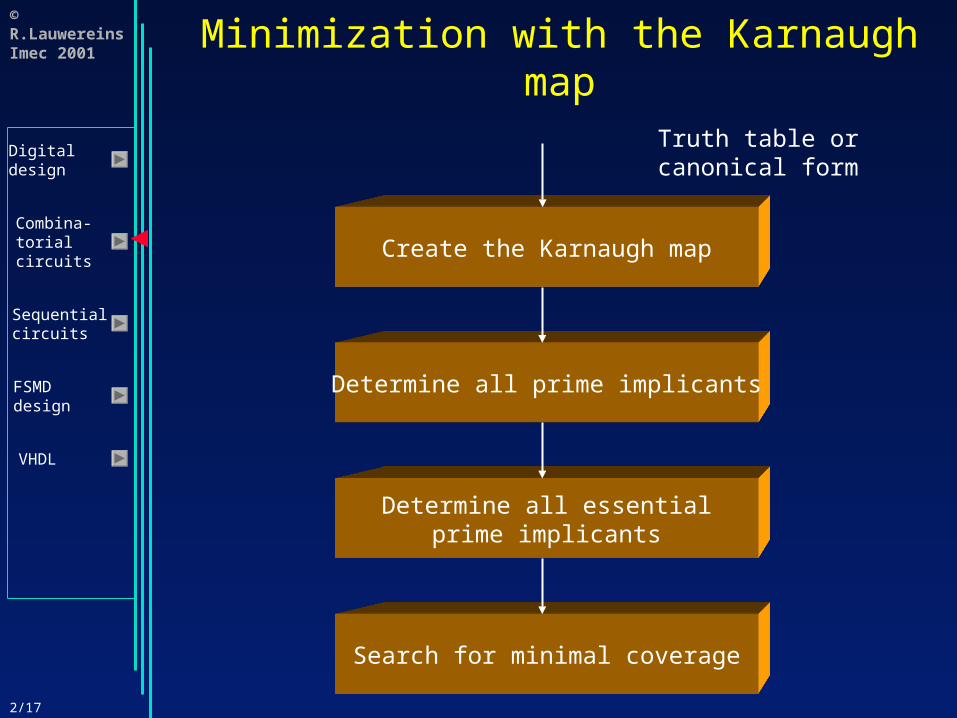
Minimization with the Karnaugh map
Determine all prime implicants
Determine all essentialprime implicants
Search for minimal coverage
Create the Karnaugh map
Truth table orcanonical form
2/18
© R.LauwereinsImec 2001
Digitaldesign
Combina-torialcircuits
Sequentialcircuits
FSMDdesign
VHDL
Minimization with the Karnaugh map
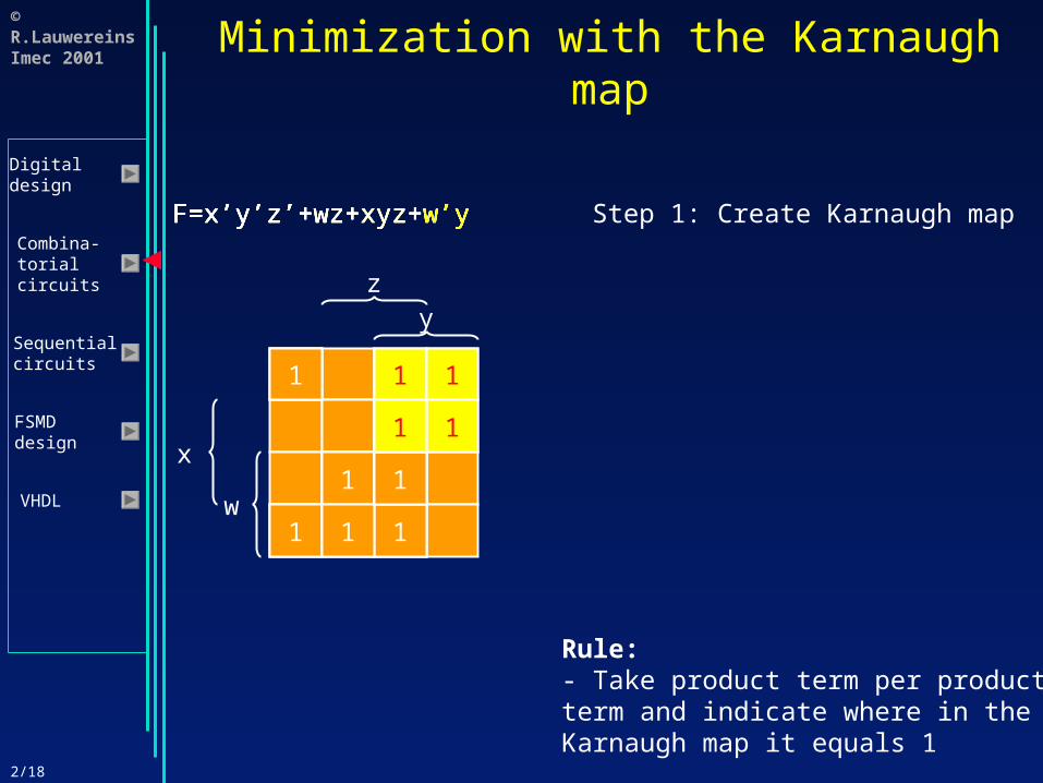
Step 1: Create Karnaugh map
w
x
yz
1
1
F=x’y’z’+wz+xyz+w’yF=x’y’z’+wz+xyz+w’yF=x’y’z’+wz+xyz+w’y
1
1
1 1
11
F=x’y’z’+wz+xyz+w’y
1 1
11
1
1
F=x’y’z’+wz+xyz+w’y
1
1
1 1
11
Rule:- Take product term per productterm and indicate where in theKarnaugh map it equals 1
2/19
© R.LauwereinsImec 2001
Digitaldesign
Combina-torialcircuits
Sequentialcircuits
FSMDdesign
VHDL
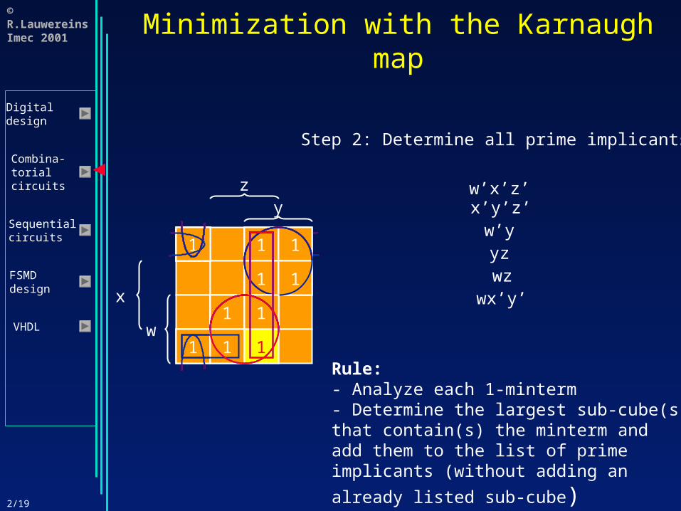
Minimization with the Karnaugh map
Step 2: Determine all prime implicants
1 1 1
1 1
1 1
1 1 1w
x
yz
11
w’x’z’x’y’z’
1 1w’yyz1 1
1
1
1 11
1
wz
1 11
1
wx’y’
1 11 1Rule:- Analyze each 1-minterm- Determine the largest sub-cube(s)that contain(s) the minterm andadd them to the list of primeimplicants (without adding an
already listed sub-cube)
2/20
© R.LauwereinsImec 2001
Digitaldesign
Combina-torialcircuits
Sequentialcircuits
FSMDdesign
VHDL
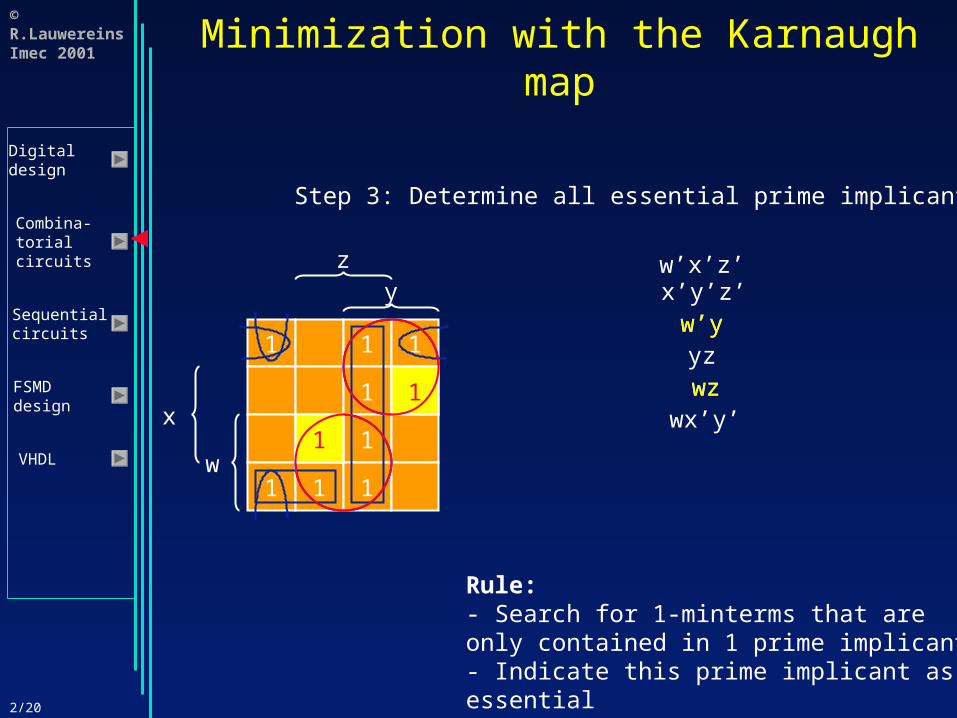
Minimization with the Karnaugh map
Step 3: Determine all essential prime implicants
1 1 1
1 1
1 1
1 1 1w
x
yz w’x’z’
x’y’z’w’yyzwz
wx’y’1
1
wz
w’y
Rule:- Search for 1-minterms that areonly contained in 1 prime implicant- Indicate this prime implicant asessential
2/21
© R.LauwereinsImec 2001
Digitaldesign
Combina-torialcircuits
Sequentialcircuits
FSMDdesign
VHDL
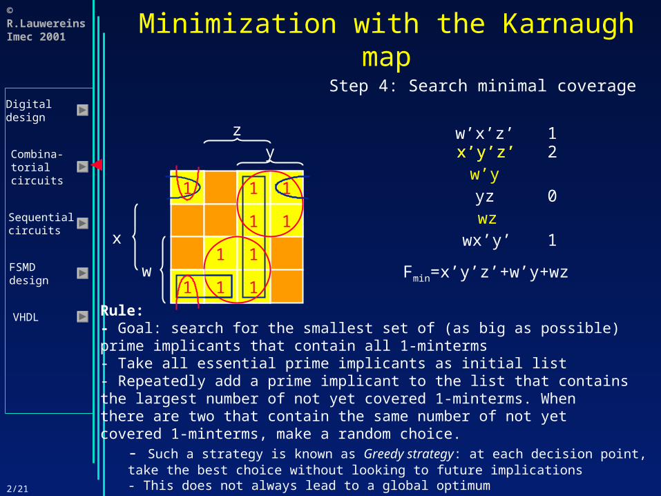
Minimization with the Karnaugh map
Step 4: Search minimal coverage
w’x’z’x’y’z’w’yyzwz
wx’y’
1 1 1
1 1
1 1
1 1 1w
x
yz
1 1
1 1
1 1
1 1
12
0
1
1
1
x’y’z’
Fmin=x’y’z’+w’y+wz
Rule:- Goal: search for the smallest set of (as big as possible)prime implicants that contain all 1-minterms- Take all essential prime implicants as initial list- Repeatedly add a prime implicant to the list that containsthe largest number of not yet covered 1-minterms. Whenthere are two that contain the same number of not yetcovered 1-minterms, make a random choice.
- Such a strategy is known as Greedy strategy: at each decision point,take the best choice without looking to future implications- This does not always lead to a global optimum
2/22
© R.LauwereinsImec 2001
Digitaldesign
Combina-torialcircuits
Sequentialcircuits
FSMDdesign
VHDL
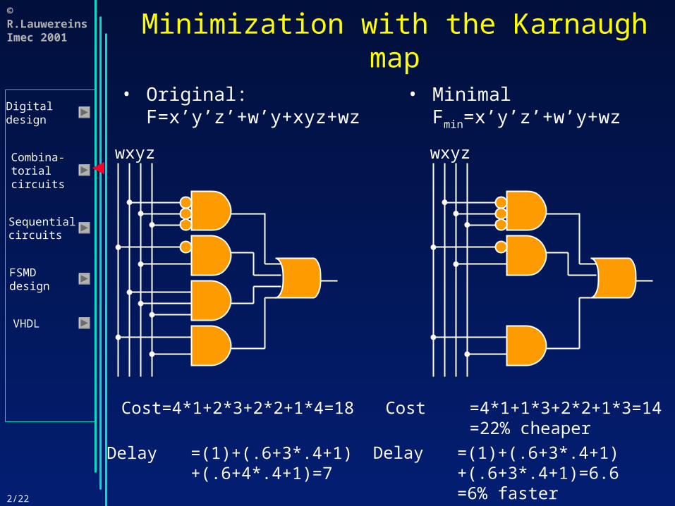
Minimization with the Karnaugh map
• Original:F=x’y’z’+w’y+xyz+wz
• MinimalFmin=x’y’z’+w’y+wz
wxyz wxyz
Cost=4*1+2*3+2*2+1*4=18 Cost =4*1+1*3+2*2+1*3=14=22% cheaper
Delay =(1)+(.6+3*.4+1)+(.6+4*.4+1)=7
Delay =(1)+(.6+3*.4+1)+(.6+3*.4+1)=6.6=6% faster

2/23
© R.LauwereinsImec 2001
Digitaldesign
Combina-torialcircuits
Sequentialcircuits
FSMDdesign
VHDL
Minimization with the Karnaugh map
• Example 2: F(v,w,x,y,z)v w x y z F
0 0 0 0 0 00 0 0 0 1 0
0 0 0 1 0 0
0 0 0 1 1 0
0 0 1 0 0 0
0 0 1 0 1 0
0 0 1 1 0 1
0 0 1 1 1 1
0 1 0 0 0 0
0 1 0 0 1 0
0 1 0 1 0 1
0 1 0 1 1 1
0 1 1 0 0 0
0 1 1 0 1 0
0 1 1 1 0 1
0 1 1 1 1 1
v w x y z F
1 0 0 0 0 0
1 0 0 0 1 0
1 0 0 1 0 0
1 0 0 1 1 0
1 0 1 0 0 0
1 0 1 0 1 1
1 0 1 1 0 0
1 0 1 1 1 1
1 1 0 0 0 0
1 1 0 0 1 1
1 1 0 1 0 0
1 1 0 1 1 1
1 1 1 0 0 0
1 1 1 0 1 1
1 1 1 1 0 0
1 1 1 1 1 1
2/24
© R.LauwereinsImec 2001
Digitaldesign
Combina-torialcircuits
Sequentialcircuits
FSMDdesign
VHDL
Minimization with the Karnaugh map
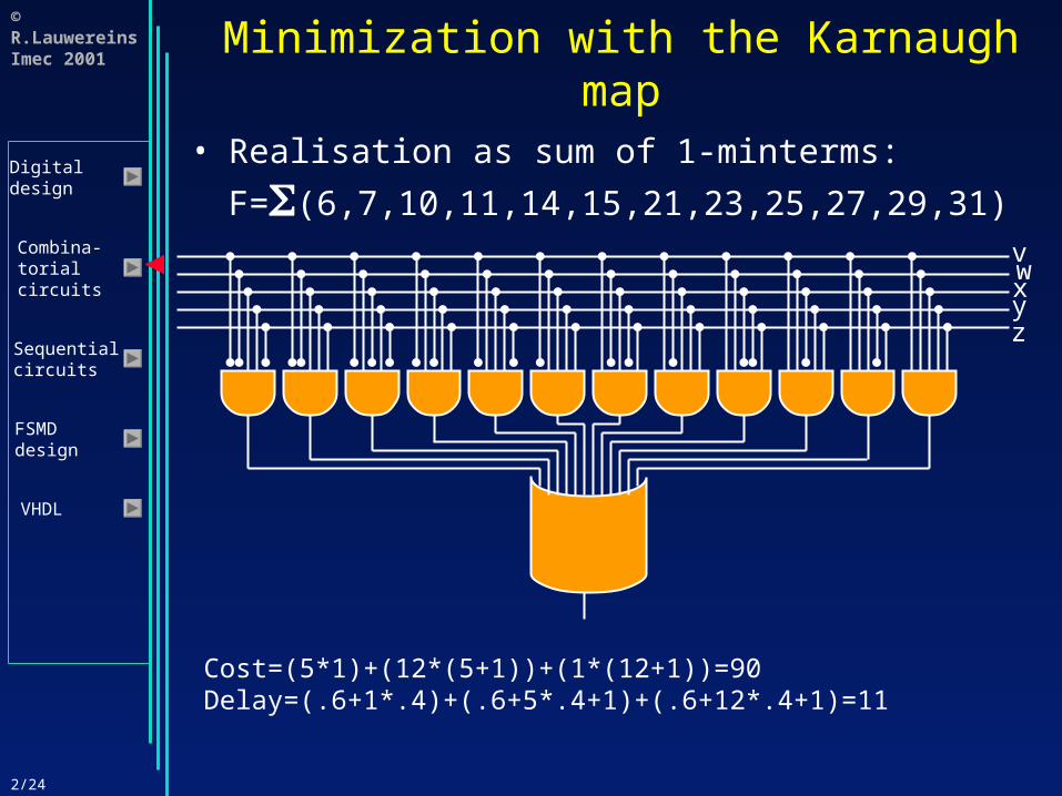
• Realisation as sum of 1-minterms:
F=(6,7,10,11,14,15,21,23,25,27,29,31)vwxyz
Cost=(5*1)+(12*(5+1))+(1*(12+1))=90Delay=(.6+1*.4)+(.6+5*.4+1)+(.6+12*.4+1)=11
2/25
© R.LauwereinsImec 2001
Digitaldesign
Combina-torialcircuits
Sequentialcircuits
FSMDdesign
VHDL
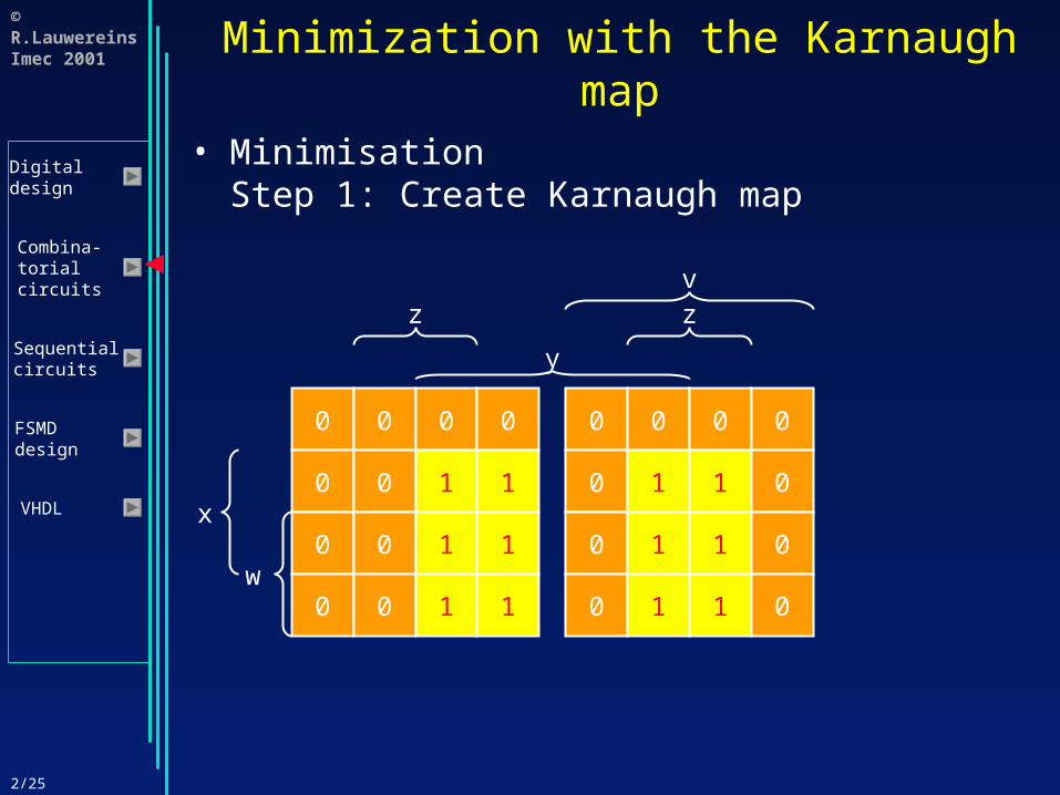
Minimization with the Karnaugh map
• MinimisationStep 1: Create Karnaugh map
0 0 0 0
0 0 1 1
0 0 1 1
0 0 1 1
0 0 0 0
0 1 1 0
0 1 1 0
0 1 1 0w
x
y
z zv
2/26
© R.LauwereinsImec 2001
Digitaldesign
Combina-torialcircuits
Sequentialcircuits
FSMDdesign
VHDL
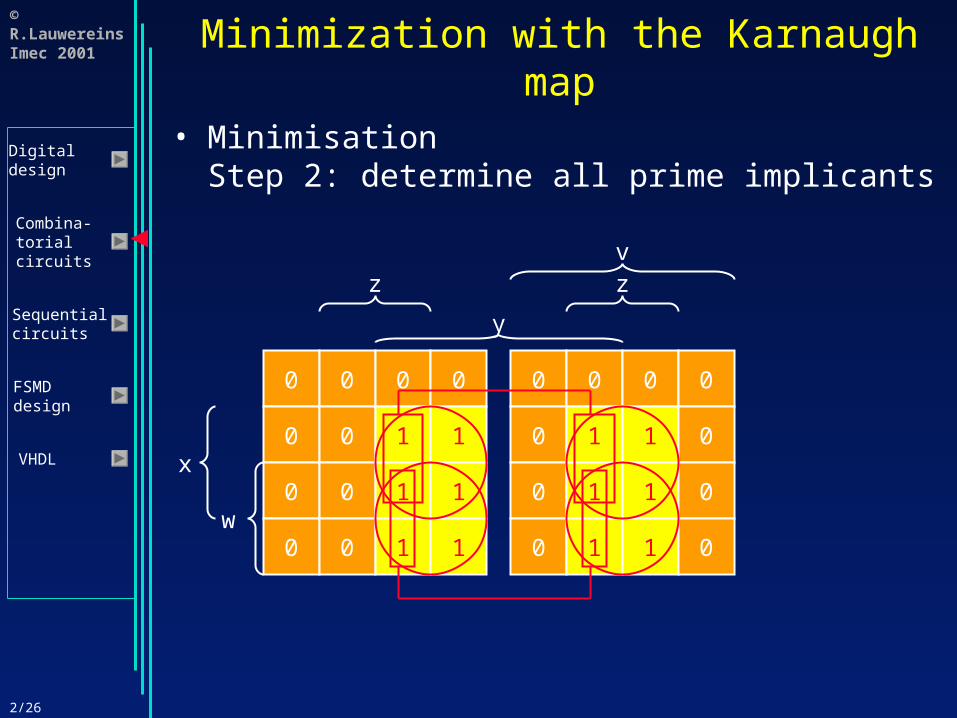
Minimization with the Karnaugh map
• MinimisationStep 2: determine all prime implicants
0 0 0 0
0 0 1 1
0 0 1 1
0 0 1 1
0 0 0 0
0 1 1 0
0 1 1 0
0 1 1 0w
x
y
z zv

2/27
© R.LauwereinsImec 2001
Digitaldesign
Combina-torialcircuits
Sequentialcircuits
FSMDdesign
VHDL1 1
11
1 1
11
Minimization with the Karnaugh map
• MinimisationStep 3: Determine all essential prime implicants
0 0 0 0
0 0
0 0 1 1
0 0
0 0 0 0
0 0
0 1 1 0
0 0w
x
y
z zv
1
1
1
1
F1min2=v’xy+v’wy+vxz+vwz
Is already the minimum coverage
2/28
© R.LauwereinsImec 2001
Digitaldesign
Combina-torialcircuits
Sequentialcircuits
FSMDdesign
VHDL
Minimization with the Karnaugh map
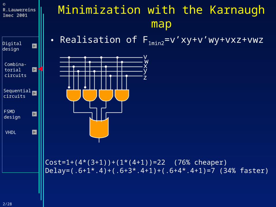
• Realisation of F1min2=v’xy+v’wy+vxz+vwz
vwxyz
Cost=1+(4*(3+1))+(1*(4+1))=22 (76% cheaper)Delay=(.6+1*.4)+(.6+3*.4+1)+(.6+4*.4+1)=7 (34% faster)
2/29
© R.LauwereinsImec 2001
Digitaldesign
Combina-torialcircuits
Sequentialcircuits
FSMDdesign
VHDL
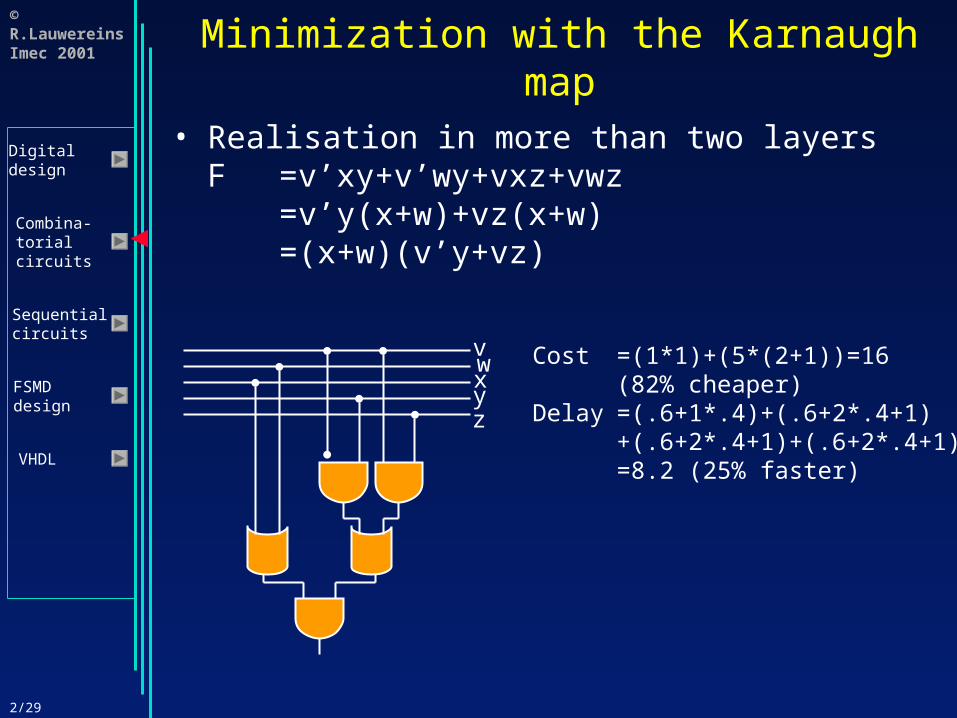
Minimization with the Karnaugh map
• Realisation in more than two layers F =v’xy+v’wy+vxz+vwz
=v’y(x+w)+vz(x+w)=(x+w)(v’y+vz)
vwxyz
Cost =(1*1)+(5*(2+1))=16(82% cheaper)
Delay =(.6+1*.4)+(.6+2*.4+1)+(.6+2*.4+1)+(.6+2*.4+1)=8.2 (25% faster)

2/30
© R.LauwereinsImec 2001
Digitaldesign
Combina-torialcircuits
Sequentialcircuits
FSMDdesign
VHDL
Minimization with the Karnaugh map
• Dual minimisationStep 1: Create the Karnaugh map
0 0 0 0
0 0 1 1
0 0 1 1
0 0 1 1
0 0 0 0
0 1 1 0
0 1 1 0
0 1 1 0w
x
y
z zv

2/31
© R.LauwereinsImec 2001
Digitaldesign
Combina-torialcircuits
Sequentialcircuits
FSMDdesign
VHDL
Minimization with the Karnaugh map
• Dual minimisationStep 2: Determine all prime implicants
0 0 0 0
0 0 1 1
0 0 1 1
0 0 1 1
0 0 0 0
0 1 1 0
0 1 1 0
0 1 1 0w
x
y
z zv

2/32
© R.LauwereinsImec 2001
Digitaldesign
Combina-torialcircuits
Sequentialcircuits
FSMDdesign
VHDL
Minimization with the Karnaugh map
• Dual minimisationStep 3: Determine all essential prime implicants
0 0 0 0
0 0 1 1
0 0 1 1
0 0 1 1
0 0 0 0
0 1 1 0
0 1 1 0
0 1 1 0w
x
y
z zv
0
0
0
0 0
0
0
0
00
Is already the minimum coverageF0min2=(v+y)(w+x)(v’+z)

2/33
© R.LauwereinsImec 2001
Digitaldesign
Combina-torialcircuits
Sequentialcircuits
FSMDdesign
VHDL
Minimization with the Karnaugh map
• Realisation of F0min2=(v+y)(w+x)(v’+z)
vwxyz
Cost=(1*1)+(3*(2+1))+(1*(3+1))=14 (84% cheaper)Delay=(.6+1*.4)+(.6+2*.4+1)+(.6+3*.4+1)=6.2 (44% faster)
2/34
© R.LauwereinsImec 2001
Digitaldesign
Combina-torialcircuits
Sequentialcircuits
FSMDdesign
VHDL
Minimization with the Karnaugh map
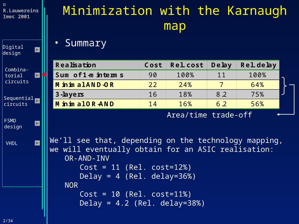
• Summary
Realisation Cost Rel. cost Delay Rel. delay
Sum of 1-minterms 90 100% 11 100%
Minimal AND-OR 22 24% 7 64%3-layers 16 18% 8.2 75%Minimal OR-AND 14 16% 6.2 56%
Area/time trade-off
We’ll see that, depending on the technology mapping, we will eventually obtain for an ASIC realisation:
OR-AND-INVCost = 11 (Rel. cost=12%)Delay = 4 (Rel. delay=36%)
NORCost = 10 (Rel. cost=11%)Delay = 4.2 (Rel. delay=38%)

2/35
© R.LauwereinsImec 2001
Digitaldesign
Combina-torialcircuits
Sequentialcircuits
FSMDdesign
VHDL
Design of Combinatorial Circuits
• Minimization of Boolean functions Karnaugh map Minimization with the Karnaugh map Don’t care conditions Quine-McCluskey
• Technology mapping• Correct timing behavior• Basic RTL building blocks (Adder, ALU, MUX,
…)
2/36
© R.LauwereinsImec 2001
Digitaldesign
Combina-torialcircuits
Sequentialcircuits
FSMDdesign
VHDL
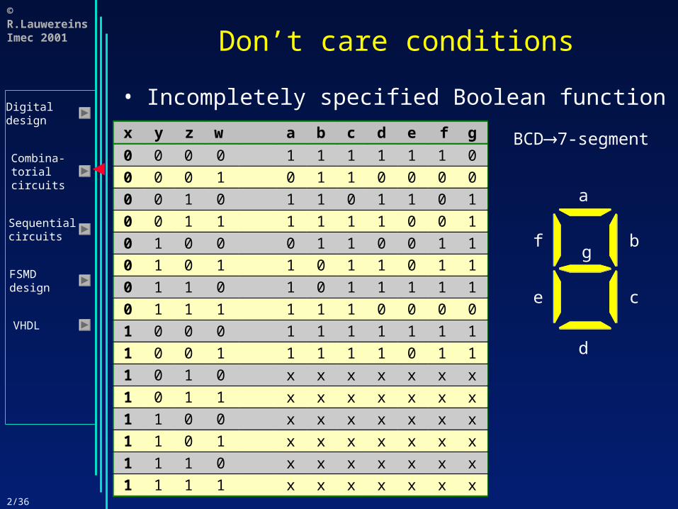
Don’t care conditions
• Incompletely specified Boolean function
BCD7-segment
a
b
c
d
e
fg
x y z w a b c d e f g
0 0 0 0 1 1 1 1 1 1 00 0 0 1
0 0 1 0
0 0 1 1
0 1 0 00 1 0 1
0 1 1 0
0 1 1 1
1 0 0 0
1 0 0 1
1 0 1 0
1 0 1 1
1 1 0 0
1 1 0 1
1 1 1 0
1 1 1 1
x y z w a b c d e f g
0 0 0 0 1 1 1 1 1 1 00 0 0 1 0 1 1 0 0 0 0
0 0 1 0
0 0 1 1
0 1 0 00 1 0 1
0 1 1 0
0 1 1 1
1 0 0 0
1 0 0 1
1 0 1 0
1 0 1 1
1 1 0 0
1 1 0 1
1 1 1 0
1 1 1 1
x y z w a b c d e f g
0 0 0 0 1 1 1 1 1 1 00 0 0 1 0 1 1 0 0 0 0
0 0 1 0 1 1 0 1 1 0 1
0 0 1 1
0 1 0 00 1 0 1
0 1 1 0
0 1 1 1
1 0 0 0
1 0 0 1
1 0 1 0
1 0 1 1
1 1 0 0
1 1 0 1
1 1 1 0
1 1 1 1
x y z w a b c d e f g
0 0 0 0 1 1 1 1 1 1 00 0 0 1 0 1 1 0 0 0 0
0 0 1 0 1 1 0 1 1 0 1
0 0 1 1 1 1 1 1 0 0 1
0 1 0 0 0 1 1 0 0 1 10 1 0 1 1 0 1 1 0 1 1
0 1 1 0 1 0 1 1 1 1 1
0 1 1 1 1 1 1 0 0 0 0
1 0 0 0 1 1 1 1 1 1 1
1 0 0 1 1 1 1 1 0 1 1
1 0 1 0 x x x x x x x
1 0 1 1
1 1 0 0
1 1 0 1
1 1 1 0
1 1 1 1
x y z w a b c d e f g
0 0 0 0 1 1 1 1 1 1 00 0 0 1 0 1 1 0 0 0 0
0 0 1 0 1 1 0 1 1 0 1
0 0 1 1 1 1 1 1 0 0 1
0 1 0 0 0 1 1 0 0 1 1
0 1 0 1 1 0 1 1 0 1 1
0 1 1 0 1 0 1 1 1 1 1
0 1 1 1 1 1 1 0 0 0 0
1 0 0 0 1 1 1 1 1 1 1
1 0 0 1 1 1 1 1 0 1 1
1 0 1 0 x x x x x x x
1 0 1 1 x x x x x x x
1 1 0 0 x x x x x x x
1 1 0 1 x x x x x x x
1 1 1 0 x x x x x x x
1 1 1 1 x x x x x x x

2/37
© R.LauwereinsImec 2001
Digitaldesign
Combina-torialcircuits
Sequentialcircuits
FSMDdesign
VHDL
Don’t care conditions
• Step 1: Create Karnaugh maps
1 0 1 1
0 1 1 1
x x x x
1 1 x x
1 1 1 1
1 0 1 0
x x x x
1 1 x x
1 1 1 0
1 1 1 1
x x x x
1 1 x x
1 0 1 1
0 1 0 1
x x x x
1 1 x x
1 0 0 1
0 0 0 1
x x x x
1 0 x x
1 0 0 0
1 1 0 1
x x x x
1 1 x x
0 0 1 1
1 1 0 1
x x x x
1 1 x x
x
x
y
y
z z z zw w w w
a b c d
e f g

2/38
© R.LauwereinsImec 2001
Digitaldesign
Combina-torialcircuits
Sequentialcircuits
FSMDdesign
VHDL
Don’t care conditions
• Step 2: determine all prime implicants
1 0 1 1
0 1 1 1
x x x x
1 1 x x
1 1 1 1
1 0 1 0
x x x x
1 1 x x
1 1 1 0
1 1 1 1
x x x x
1 1 x x
1 0 1 1
0 1 0 1
x x x x
1 1 x x
1 0 0 1
0 0 0 1
x x x x
1 0 x x
1 0 0 0
1 1 0 1
x x x x
1 1 x x
0 0 1 1
1 1 0 1
x x x x
1 1 x x
x
x
y
y
z z z zw w w w
a b c d
e f g
2/39
© R.LauwereinsImec 2001
Digitaldesign
Combina-torialcircuits
Sequentialcircuits
FSMDdesign
VHDL
Don’t care conditions
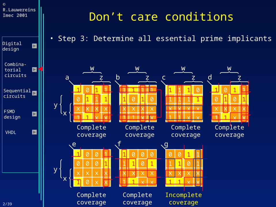
• Step 3: Determine all essential prime implicants
1 0 1 1
0 1 1 1
x x x x
1 1 x xx
y
zw
a
Completecoverage
1 1 1 0
1 1 1 1
x x x x
1 1 x x
zw
c
Completecoverage
1 0 1 1
0 1 0 1
x x x x
1 1 x x
zw
d
Completecoverage
1 0 0 1
0 0 0 1
x x x x
1 0 x xxy
e
Completecoverage
1 0 0 0
1 1 0 1
x x x x
1 1 x x
f
Completecoverage
0 0 1 1
1 1 0 1
x x x x
1 1 x x
g
Incompletecoverage
1 1 1 1
1 0 1 0
x x x x
1 1 x x
zw
b
Completecoverage
2/40
© R.LauwereinsImec 2001
Digitaldesign
Combina-torialcircuits
Sequentialcircuits
FSMDdesign
VHDL
Don’t care conditions
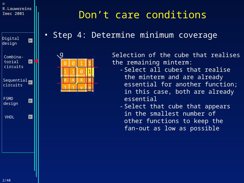
• Step 4: Determine minimum coverage
0 0 1 1
1 1 0 1
x x x x
1 1 x x
g Selection of the cube that realisesthe remaining minterm:
- Select all cubes that realisethe minterm and are alreadyessential for another function;in this case, both are alreadyessential
- Select that cube that appearsin the smallest number ofother functions to keep thefan-out as low as possible
2/41
© R.LauwereinsImec 2001
Digitaldesign
Combina-torialcircuits
Sequentialcircuits
FSMDdesign
VHDL
Don’t care conditions
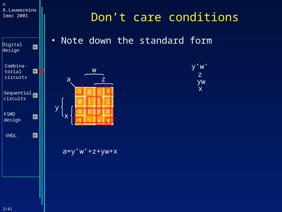
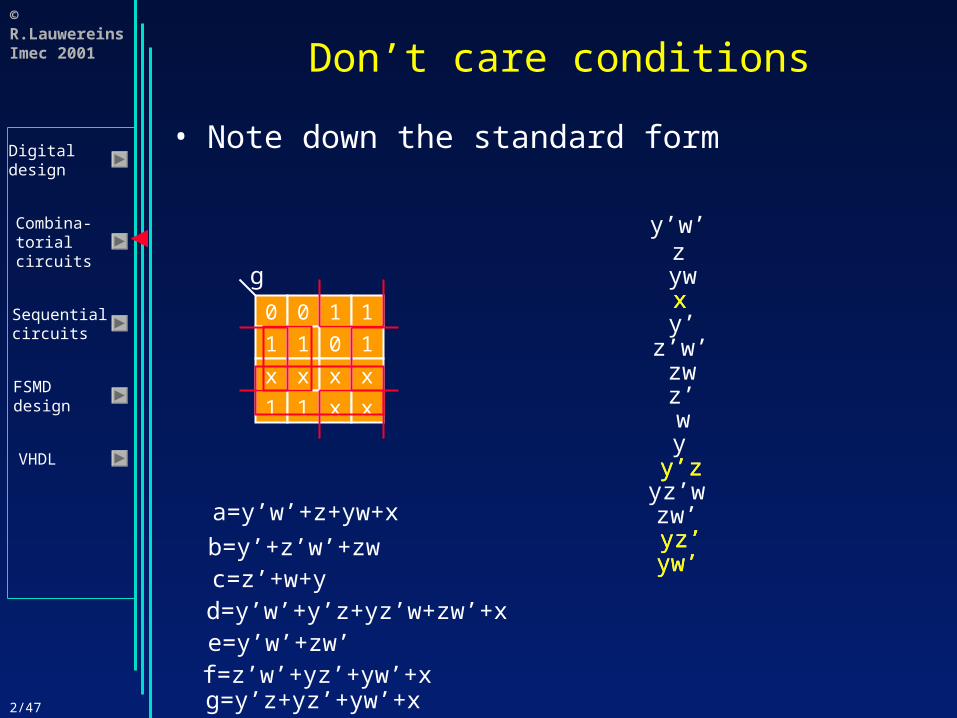
• Note down the standard form
1 0 1 1
0 1 1 1
x x x x
1 1 x xx
y
zw
a
y’w’zywx
a=y’w’+z+yw+x

2/42
© R.LauwereinsImec 2001
Digitaldesign
Combina-torialcircuits
Sequentialcircuits
FSMDdesign
VHDL
1 1 1 1
1 0 1 0
x x x x
1 1 x x
zw
b
Don’t care conditions
• Note down the standard form
y’w’zywx
a=y’w’+z+yw+x
z’w’zw
b=y’+z’w’+zw
y’

2/43
© R.LauwereinsImec 2001
Digitaldesign
Combina-torialcircuits
Sequentialcircuits
FSMDdesign
VHDL
1 1 1 0
1 1 1 1
x x x x
1 1 x x
zw
c
Don’t care conditions
• Note down the standard form
y’w’zywx
a=y’w’+z+yw+x
y’z’w’zw
b=y’+z’w’+zw
z’wy
c=z’+w+y

2/44
© R.LauwereinsImec 2001
Digitaldesign
Combina-torialcircuits
Sequentialcircuits
FSMDdesign
VHDL
1 0 1 1
0 1 0 1
x x x x
1 1 x x
zw
d
Don’t care conditions
• Note down the standard form
y’w’zywx
a=y’w’+z+yw+x
y’z’w’zw
b=y’+z’w’+zw
z’wy
c=z’+w+y
y’w’
y’zyz’wzw’
x
d=y’w’+y’z+yz’w+zw’+x
2/45
© R.LauwereinsImec 2001
Digitaldesign
Combina-torialcircuits
Sequentialcircuits
FSMDdesign
VHDL
1 0 0 1
0 0 0 1
x x x x
1 0 x xxy
e
Don’t care conditions
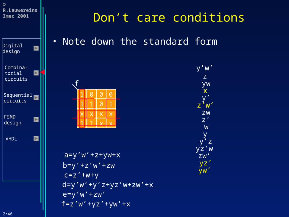
• Note down the standard form
zywx
a=y’w’+z+yw+x
y’z’w’zw
b=y’+z’w’+zw
z’wy
c=z’+w+y
y’zyz’wzw’
d=y’w’+y’z+yz’w+zw’+x
y’w’y’w’
zw’
e=y’w’+zw’
2/46
© R.LauwereinsImec 2001
Digitaldesign
Combina-torialcircuits
Sequentialcircuits
FSMDdesign
VHDL
1 0 0 0
1 1 0 1
x x x x
1 1 x x
f
Don’t care conditions
• Note down the standard form
zywx
a=y’w’+z+yw+x
y’z’w’zw
b=y’+z’w’+zw
z’wy
c=z’+w+y
y’zyz’wzw’
d=y’w’+y’z+yz’w+zw’+xe=y’w’+zw’
z’w’
yz’yw’
x
f=z’w’+yz’+yw’+x
y’w’
2/47
© R.LauwereinsImec 2001
Digitaldesign
Combina-torialcircuits
Sequentialcircuits
FSMDdesign
VHDL
0 0 1 1
1 1 0 1
x x x x
1 1 x x
g
Don’t care conditions
• Note down the standard form
zywx
a=y’w’+z+yw+x
y’z’w’zw
b=y’+z’w’+zw
z’wy
c=z’+w+y
y’zyz’wzw’
d=y’w’+y’z+yz’w+zw’+xe=y’w’+zw’
yz’yw’
f=z’w’+yz’+yw’+x
yz’
y’z
yw’
x
g=y’z+yz’+yw’+x
y’w’

2/48
© R.LauwereinsImec 2001
Digitaldesign
Combina-torialcircuits
Sequentialcircuits
FSMDdesign
VHDL
Don’t care conditions
xyzw
a cb d e f g

2/49
© R.LauwereinsImec 2001
Digitaldesign
Combina-torialcircuits
Sequentialcircuits
FSMDdesign
VHDL
Don’t care conditions
• Cost when realising as (1-minterms): a: 4*1+8*(4+1)+1*(8+1)=53 b: 4*1+8*(4+1)+1*(8+1)=53 c: 4*1+9*(4+1)+1*(9+1)=59 d: 4*1+7*(4+1)+1*(7+1)=47 e: 4*1+4*(4+1)+1*(4+1)=29 f: 4*1+6*(4+1)+1*(6+1)=41 g: 4*1+7*(4+1)+1*(7+1)=47
• Cost for minimal 2-layer-implementation Invertors: 4*1=4 AND-gates: 8*(2+1)+1*(3+1)=28 OR-gates: 1*(2+1)+2*(3+1)+3*(4+1)
+1*(5+1)=32
329 (100%)
64 (19%)
2/50
© R.LauwereinsImec 2001
Digitaldesign
Combina-torialcircuits
Sequentialcircuits
FSMDdesign
VHDL
Don’t care conditions
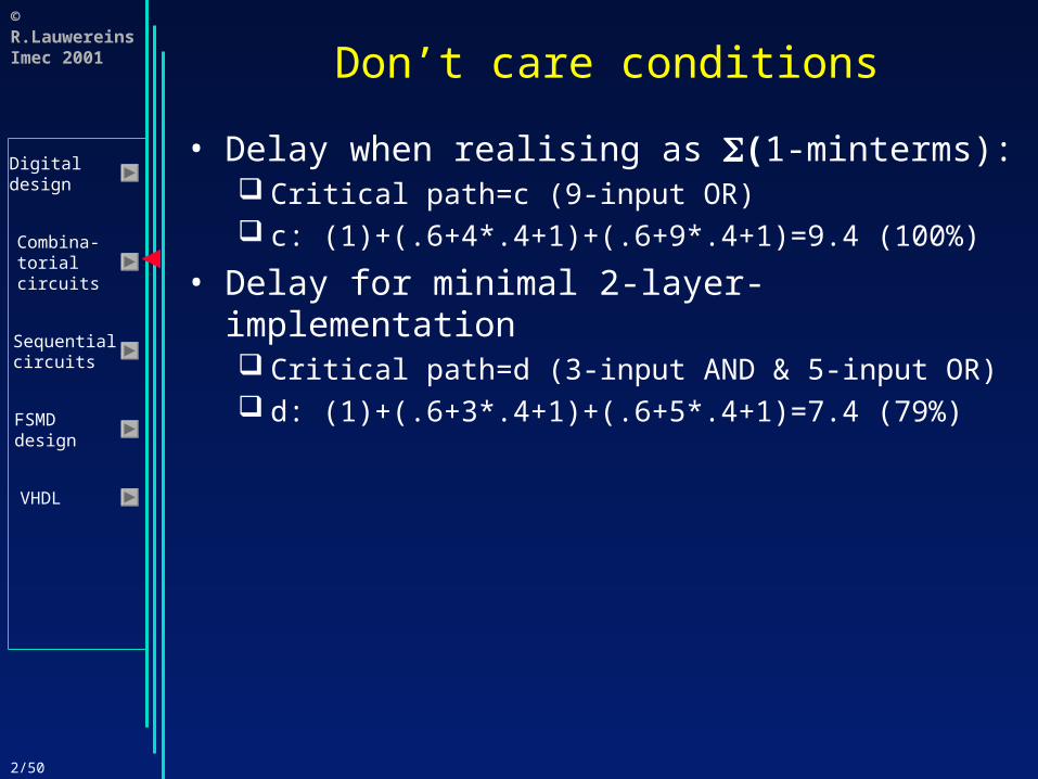
• Delay when realising as (1-minterms): Critical path=c (9-input OR) c: (1)+(.6+4*.4+1)+(.6+9*.4+1)=9.4 (100%)
• Delay for minimal 2-layer-implementation Critical path=d (3-input AND & 5-input OR) d: (1)+(.6+3*.4+1)+(.6+5*.4+1)=7.4 (79%)
2/51
© R.LauwereinsImec 2001
Digitaldesign
Combina-torialcircuits
Sequentialcircuits
FSMDdesign
VHDL
Design of Combinatorial Circuits
• Minimization of Boolean functions Karnaugh map Minimization with the Karnaugh map Don’t care conditions Quine-McCluskey
• Technology mapping• Correct timing behavior• Basic RTL building blocks (Adder, ALU, MUX,
…)
2/52
© R.LauwereinsImec 2001
Digitaldesign
Combina-torialcircuits
Sequentialcircuits
FSMDdesign
VHDL
Quine-McCluskey
• Method with Karnaugh map OK for human minimisation : visually oriented no guarantee for optimum solution
• Computer method Quine-McCluskey table oriented leads to optimum solution is the basis of all CAD circuit design tools hardly doable by hand

2/53
© R.LauwereinsImec 2001
Digitaldesign
Combina-torialcircuits
Sequentialcircuits
FSMDdesign
VHDL
Design of Combinatorial Circuits
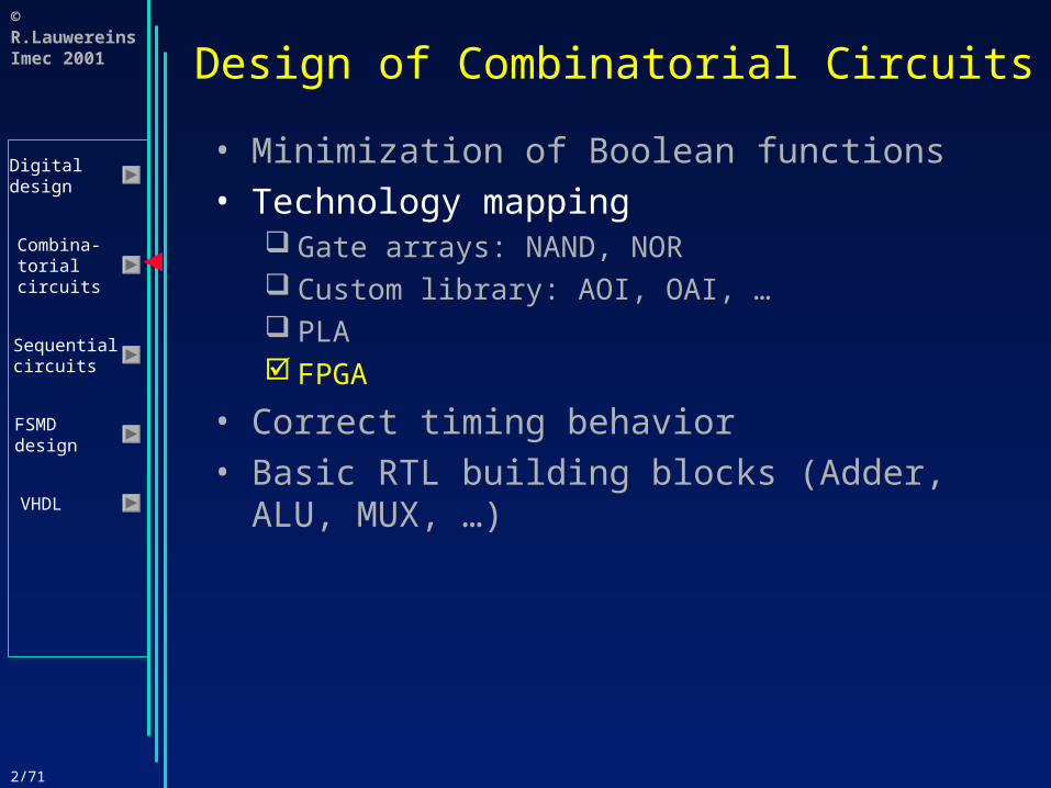
• Minimization of Boolean functions• Technology mapping
Gate arrays: NAND, NOR Custom library: AOI, OAI, … PLA FPGA
• Correct timing behavior• Basic RTL building blocks (Adder, ALU, MUX,
…)
2/54
© R.LauwereinsImec 2001
Digitaldesign
Combina-torialcircuits
Sequentialcircuits
FSMDdesign
VHDL
Design of Combinatorial Circuits
• Minimization of Boolean functions• Technology mapping
Gate arrays: NAND, NOR Custom library: AOI, OAI, … PLA FPGA
• Correct timing behavior• Basic RTL building blocks (Adder, ALU, MUX,
…)

2/55
© R.LauwereinsImec 2001
Digitaldesign
Combina-torialcircuits
Sequentialcircuits
FSMDdesign
VHDL
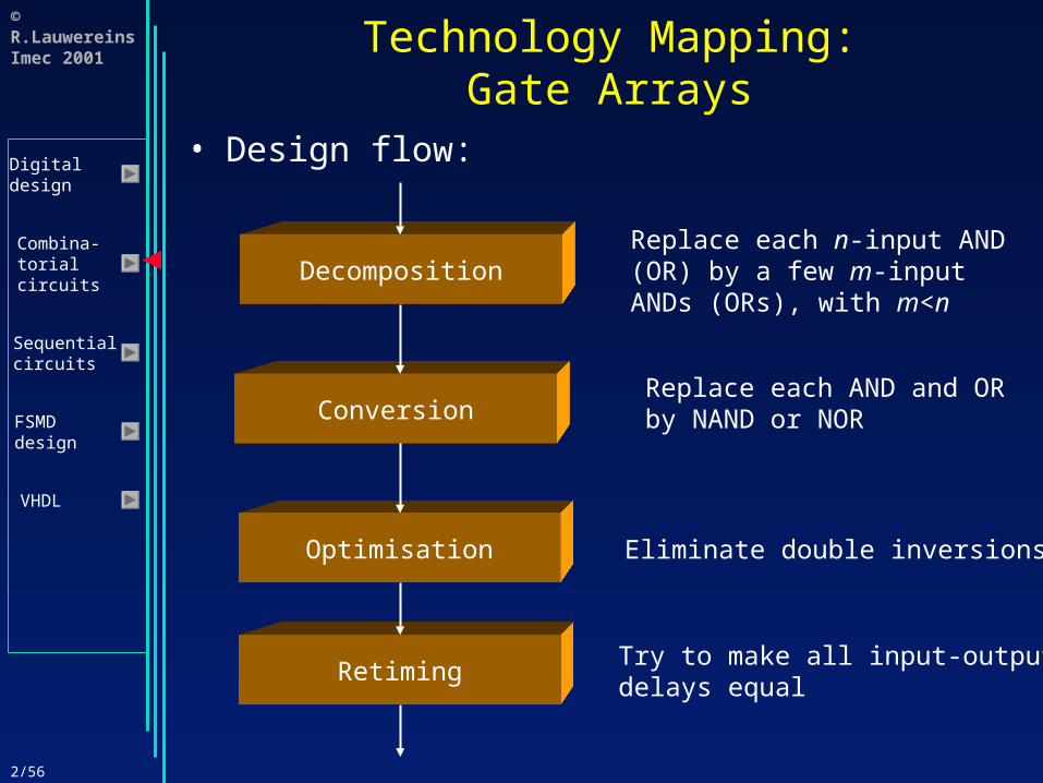
Technology Mapping:Gate Arrays
• Properties of the methodology followed: When minimizing 1-minterms: INV-AND-OR When minimizing 0-maxterms: INV-OR-AND Any function can be realized in two layers of logic
with this methodology The fan-in of the gates can become arbitrary large
• Properties of gate arrays: They only contain m-input NAND or m-input NOR
gates
• Technology mapping is: Translating a circuit consisting of INV-AND-OR to
one with only m-input NAND Dual: INV-OR-AND m-input NOR
2/56
© R.LauwereinsImec 2001
Digitaldesign
Combina-torialcircuits
Sequentialcircuits
FSMDdesign
VHDL
Technology Mapping:Gate Arrays
• Design flow:
ConversionReplace each AND and ORby NAND or NOR
Optimisation Eliminate double inversions
Replace each n-input AND(OR) by a few m-inputANDs (ORs), with m<n
Decomposition
RetimingTry to make all input-outputdelays equal
2/57
© R.LauwereinsImec 2001
Digitaldesign
Combina-torialcircuits
Sequentialcircuits
FSMDdesign
VHDL
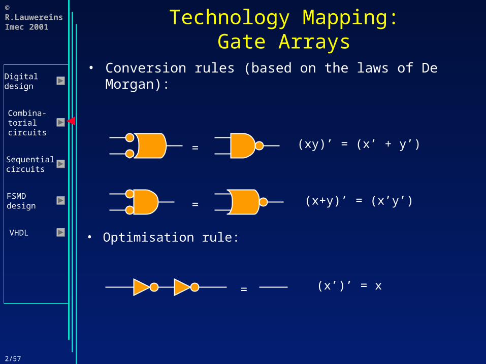
Technology Mapping:Gate Arrays
• Conversion rules (based on the laws of De Morgan):
= (xy)’ = (x’ + y’)
= (x+y)’ = (x’y’)
• Optimisation rule:
= (x’)’ = x
2/58
© R.LauwereinsImec 2001
Digitaldesign
Combina-torialcircuits
Sequentialcircuits
FSMDdesign
VHDL
Technology Mapping:Gate Arrays
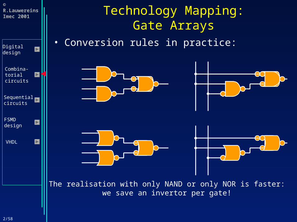
• Conversion rules in practice:
The realisation with only NAND or only NOR is faster:we save an invertor per gate!

2/59
© R.LauwereinsImec 2001
Digitaldesign
Combina-torialcircuits
Sequentialcircuits
FSMDdesign
VHDL
Technology Mapping:Gate Arrays
• Realisation of an invertor:
=
2/60
© R.LauwereinsImec 2001
Digitaldesign
Combina-torialcircuits
Sequentialcircuits
FSMDdesign
VHDL
Technology Mapping:Gate Arrays
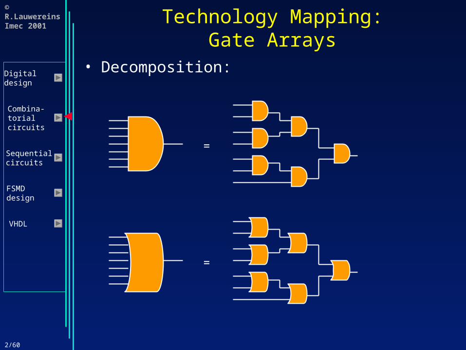
• Decomposition:
=
=
2/61
© R.LauwereinsImec 2001
Digitaldesign
Combina-torialcircuits
Sequentialcircuits
FSMDdesign
VHDL
Technology Mapping:Gate Arrays
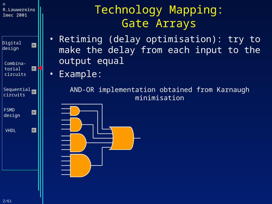
• Retiming (delay optimisation): try to make the delay from each input to the output equal
• Example:
AND-OR implementation obtained from Karnaughminimisation
2/62
© R.LauwereinsImec 2001
Digitaldesign
Combina-torialcircuits
Sequentialcircuits
FSMDdesign
VHDL
Technology Mapping:Gate Arrays
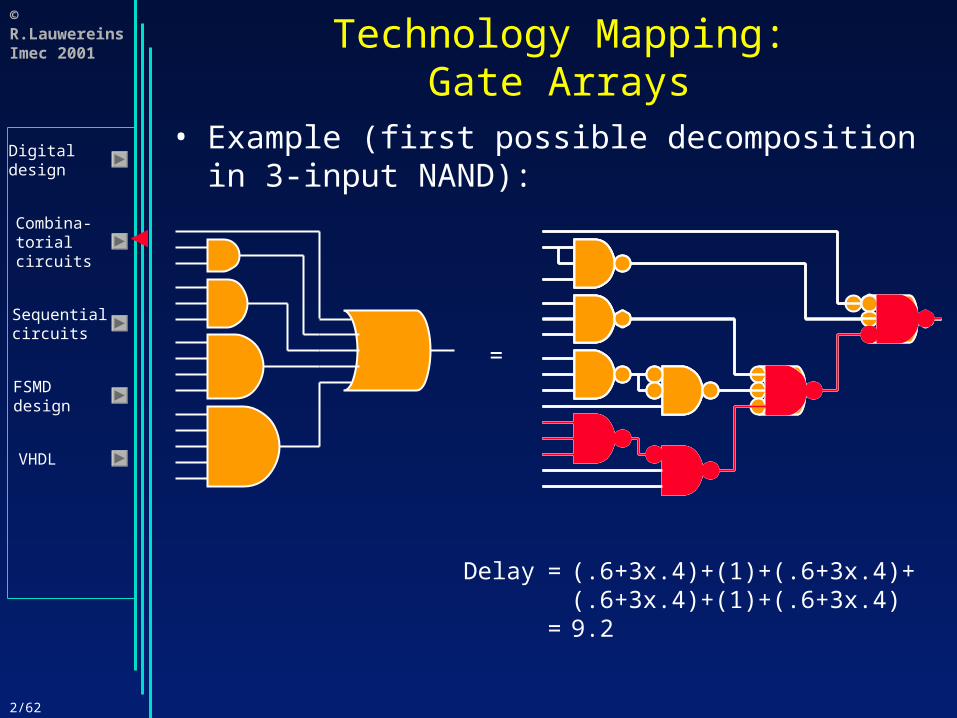
• Example (first possible decomposition in 3-input NAND):
=
Delay =(.6+3x.4)+(1)+(.6+3x.4)+(.6+3x.4)+(1)+(.6+3x.4)
=9.2
2/63
© R.LauwereinsImec 2001
Digitaldesign
Combina-torialcircuits
Sequentialcircuits
FSMDdesign
VHDL
Technology Mapping:Gate Arrays
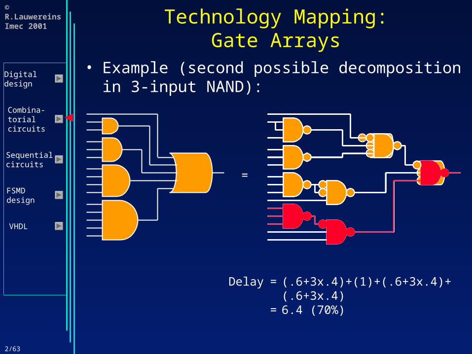
• Example (second possible decomposition in 3-input NAND):
=
Delay =(.6+3x.4)+(1)+(.6+3x.4)+(.6+3x.4)
=6.4 (70%)
2/64
© R.LauwereinsImec 2001
Digitaldesign
Combina-torialcircuits
Sequentialcircuits
FSMDdesign
VHDL
Design of Combinatorial Circuits
• Minimization of Boolean functions• Technology mapping
Gate arrays: NAND, NOR Custom library: AOI, OAI, … PLA FPGA
• Correct timing behavior• Basic RTL building blocks (Adder, ALU, MUX,
…)

2/65
© R.LauwereinsImec 2001
Digitaldesign
Combina-torialcircuits
Sequentialcircuits
FSMDdesign
VHDL
Technology Mapping:Custom Library
• ASICs have AOI en OAI: small and fast!• For small functions (not in course book):
Realise the inverse function with AND-OR or OR-AND
• Example: realise again following function:
F=(6,7,10,11,14,15,21,23,25,27,29,31) Realisation as sum of 1-minterms: cost = 90; delay
= 11 Minimal realisation as OR-AND: cost = 14 (16%);
delay = 6.2 (56%)
2/66
© R.LauwereinsImec 2001
Digitaldesign
Combina-torialcircuits
Sequentialcircuits
FSMDdesign
VHDL
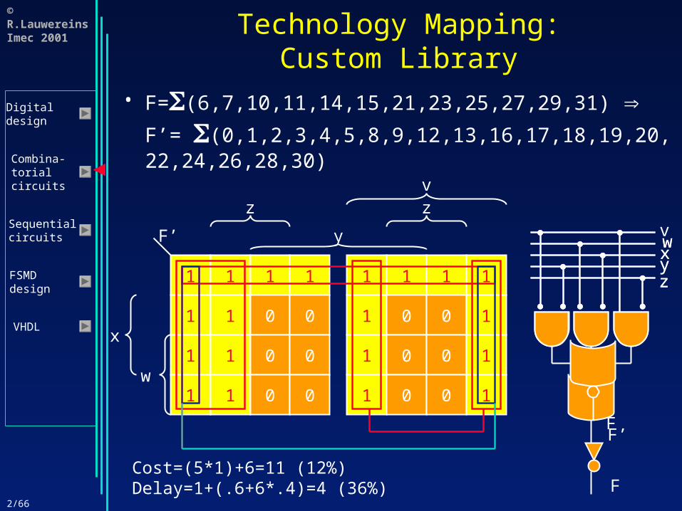
Technology Mapping:Custom Library
• F=(6,7,10,11,14,15,21,23,25,27,29,31)
F’= (0,1,2,3,4,5,8,9,12,13,16,17,18,19,20, 22,24,26,28,30)
1 1 1 1
1 1 0 0
1 1 0 0
1 1 0 0
1 1 1 1
1 0 0 1
1 0 0 1
1 0 0 1w
x
y
z zv
F’ vwxyz
F’
F
wxyz
F
Cost=(5*1)+6=11 (12%)Delay=1+(.6+6*.4)=4 (36%)
2/67
© R.LauwereinsImec 2001
Digitaldesign
Combina-torialcircuits
Sequentialcircuits
FSMDdesign
VHDL
Technology Mapping:Custom Library
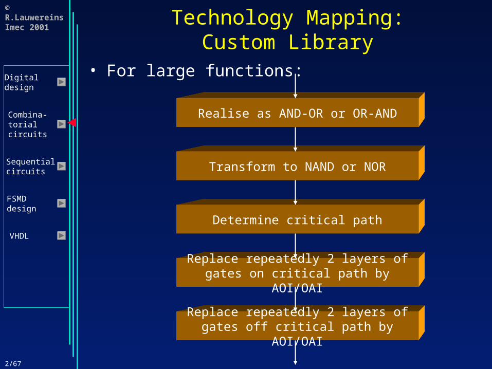
• For large functions:
Transform to NAND or NOR
Realise as AND-OR or OR-AND
Replace repeatedly 2 layers of gates off critical path by AOI/OAI
Determine critical path
Replace repeatedly 2 layers of gates on critical path by AOI/OAI
2/68
© R.LauwereinsImec 2001
Digitaldesign
Combina-torialcircuits
Sequentialcircuits
FSMDdesign
VHDL
Technology Mapping:Custom Library
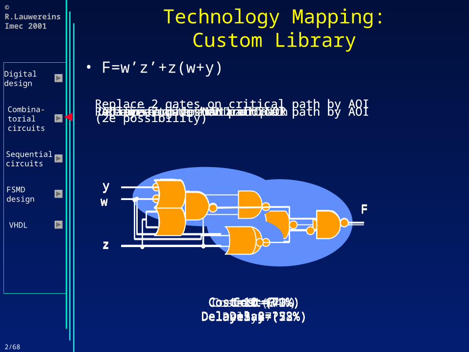
• F=w’z’+z(w+y)
Realise with AND and OR
y
z
wF
Cost=14Delay=7.2
Transform to NAND and NOR
y
z
wF
Cost=?Delay=?
Transform to NAND and NOR
y
z
wF
Cost=11 (79%)Delay=5.2 (72%)
Determine the critical path
y
z
wF
Cost=11 (79%)Delay=5.2 (72%)
Replace 2 gates on critical path by AOI
y
z
wF
Cost=?Delay=?
Replace 2 gates on critical path by AOI
y
z
wF
Cost=10 (71%)Delay=5.6 (78%)
Replace 2 gates on critical path by AOI(2e possibility)
y
z
wF
Cost=?Delay=?
Replace 2 gates on critical path by AOI(2e possibility)
y
z
wF
Cost=10 (71%)Delay=3.8 (53%)
Analyze the other path
y
z
wF
Cost=10 (71%)Delay=3.8 (53%)
Analyze the other path
y
z
wF
Cost=9 (64%)Delay=3.8 (53%)

2/69
© R.LauwereinsImec 2001
Digitaldesign
Combina-torialcircuits
Sequentialcircuits
FSMDdesign
VHDL
Design of Combinatorial Circuits
• Minimization of Boolean functions• Technology mapping
Gate arrays: NAND, NOR Custom library: AOI, OAI, … PLA FPGA
• Correct timing behavior• Basic RTL building blocks (Adder, ALU, MUX,
…)
2/70
© R.LauwereinsImec 2001
Digitaldesign
Combina-torialcircuits
Sequentialcircuits
FSMDdesign
VHDL
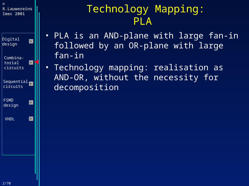
Technology Mapping:PLA
• PLA is an AND-plane with large fan-in followed by an OR-plane with large fan-in
• Technology mapping: realisation as AND-OR, without the necessity for decomposition
2/71
© R.LauwereinsImec 2001
Digitaldesign
Combina-torialcircuits
Sequentialcircuits
FSMDdesign
VHDL
Design of Combinatorial Circuits
• Minimization of Boolean functions• Technology mapping
Gate arrays: NAND, NOR Custom library: AOI, OAI, … PLA FPGA
• Correct timing behavior• Basic RTL building blocks (Adder, ALU, MUX,
…)

2/72
© R.LauwereinsImec 2001
Digitaldesign
Combina-torialcircuits
Sequentialcircuits
FSMDdesign
VHDL
Technology Mapping:FPGA
• CLB is 2 functions of 4 variables or 1 function of 5 variables
• Technology mapping is similar as for custom design but i.o. AOI/OAI we search for sub-circuits of 4 or 5 variables, first on the critical path, next on the other paths
• For FPGAs technology mapping is done by automatic tools (see next slide); when prototype: no hand optimalisation, when final product: hand optimalisation beneficial. Also for ASICs automatic tools exist, hand optimalisation is beneficial
• BCD7-segment: create 7 truth tables i.f.o. 4 variables: the rest is done by the tools

2/73
© R.LauwereinsImec 2001
Digitaldesign
Combina-torialcircuits
Sequentialcircuits
FSMDdesign
VHDL
Technology mapping:FPGA
Technologymapping
2/74
© R.LauwereinsImec 2001
Digitaldesign
Combina-torialcircuits
Sequentialcircuits
FSMDdesign
VHDL
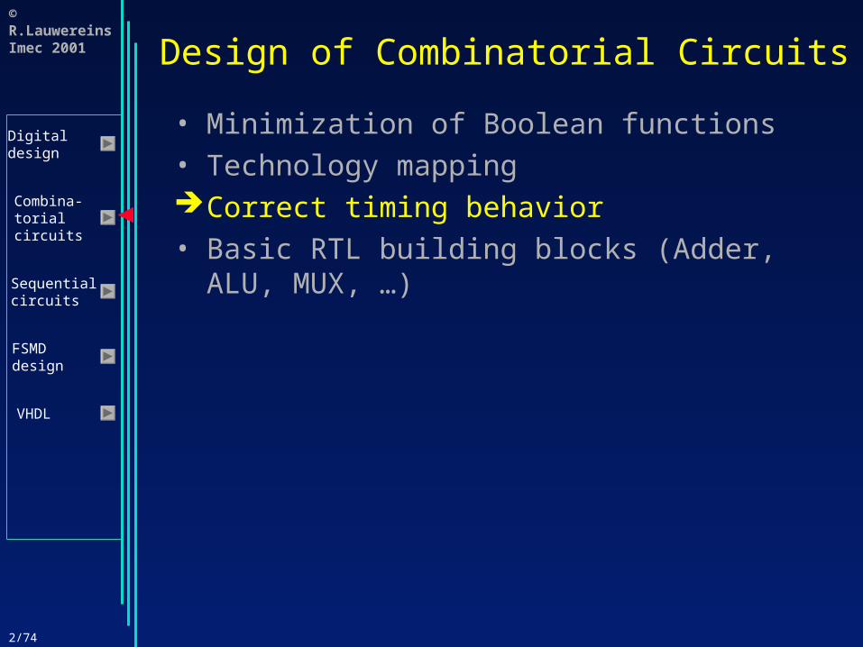
Design of Combinatorial Circuits
• Minimization of Boolean functions• Technology mappingCorrect timing behavior• Basic RTL building blocks (Adder, ALU, MUX,
…)

2/75
© R.LauwereinsImec 2001
Digitaldesign
Combina-torialcircuits
Sequentialcircuits
FSMDdesign
VHDL
Correct timing behavior:Hazard-free design
1
1 1 1x
yz
x
y
z
y’a
b
F
x
y
y’
z
a
b
F
1
x
y
z
y’a
b
F
1 1
0 1 2 3 4 5 6
x
y
z
y’a
b
Fx
y
z
y’a
b
Fx
y
z
y’a
b
Fx
y
z
y’a
b
Fx
y
z
y’a
b
Fx
y
z
y’a
b
F
Static 1-hazard
2/76
© R.LauwereinsImec 2001
Digitaldesign
Combina-torialcircuits
Sequentialcircuits
FSMDdesign
VHDL
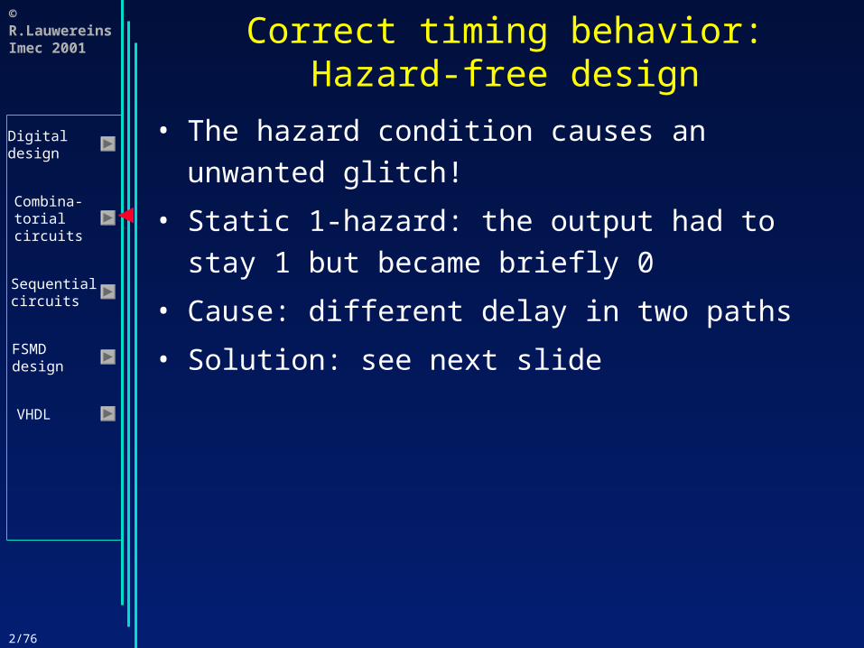
Correct timing behavior:Hazard-free design
• The hazard condition causes an unwanted glitch!
• Static 1-hazard: the output had to stay 1 but became briefly 0
• Cause: different delay in two paths
• Solution: see next slide

2/77
© R.LauwereinsImec 2001
Digitaldesign
Combina-torialcircuits
Sequentialcircuits
FSMDdesign
VHDL
Correct timing behavior:Hazard-free design
1
1 1 1x
yz
x
y
z
y’a
bF
c1
x
y
y’
z
a
b
F
0 1 2 3 4 5 6
c
x
y
z
y’a
bF
c
x
y
z
y’a
bF
c11
x
y
z
y’a
bF
c
x
y
z
y’a
bF
c
x
y
z
y’a
bF
c
2/78
© R.LauwereinsImec 2001
Digitaldesign
Combina-torialcircuits
Sequentialcircuits
FSMDdesign
VHDL
Correct timing behavior:Hazard-free design
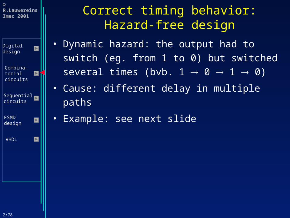
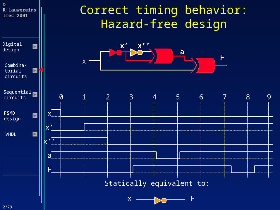
• Dynamic hazard: the output had to switch (eg. from 1 to 0) but switched several times (bvb. 1 0 1 0)
• Cause: different delay in multiple paths
• Example: see next slide
2/79
© R.LauwereinsImec 2001
Digitaldesign
Combina-torialcircuits
Sequentialcircuits
FSMDdesign
VHDL
x’ x’’a
F
x’ x’’a
Fx
Correct timing behavior:Hazard-free design
Statically equivalent to:
x F
x’’
0 1 2 3 4 5 6 7 8 9
x
x’
a
F
x’ x’’a
F
x’ x’’a
F
x’ x’’a
F
x’ x’’a
F
x’ x’’a
F
x’ x’’a
F
x’ x’’a
F
x’ x’’a
F
x’ x’’a
F
x’ x’’a
F
2/80
© R.LauwereinsImec 2001
Digitaldesign
Combina-torialcircuits
Sequentialcircuits
FSMDdesign
VHDL
Correct timing behavior:Hazard-free design
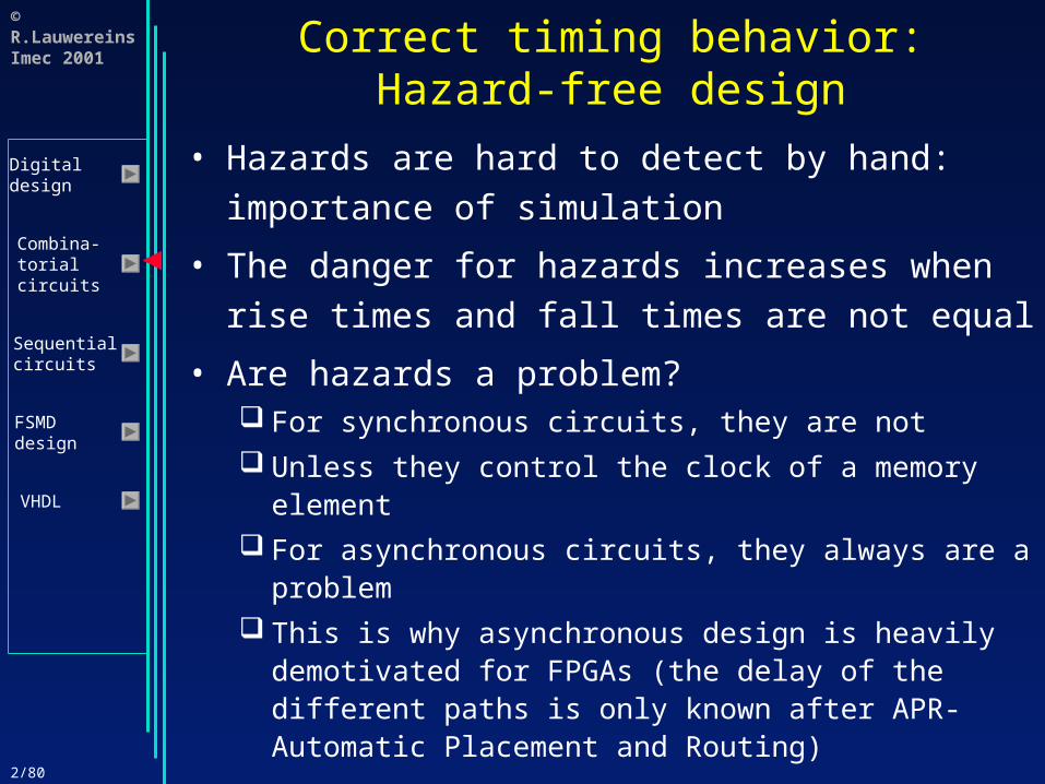
• Hazards are hard to detect by hand: importance of simulation
• The danger for hazards increases when rise times and fall times are not equal
• Are hazards a problem? For synchronous circuits, they are not Unless they control the clock of a memory element For asynchronous circuits, they always are a
problem This is why asynchronous design is heavily
demotivated for FPGAs (the delay of the different paths is only known after APR-Automatic Placement and Routing)
2/81
© R.LauwereinsImec 2001
Digitaldesign
Combina-torialcircuits
Sequentialcircuits
FSMDdesign
VHDL
Design of Combinatorial Circuits• Minimization of Boolean functions• Technology mapping• Correct timing behavior• Basic RTL building blocks
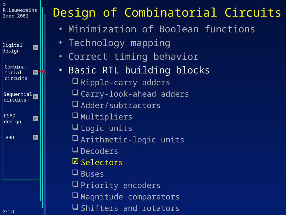
Ripple-carry adders Carry-look-ahead adders Adder/subtractors Multipliers Logic units Arithmetic-logic units Decoders Selectors Buses Priority encoders Magnitude comparators Shifters and rotators

2/82
© R.LauwereinsImec 2001
Digitaldesign
Combina-torialcircuits
Sequentialcircuits
FSMDdesign
VHDL
Design of Combinatorial Circuits• Minimization of Boolean functions• Technology mapping• Correct timing behavior• Basic RTL building blocks
Ripple-carry adders Carry-look-ahead adders Adder/subtractors Multipliers Logic units Arithmetic-logic units Decoders Selectors Buses Priority encoders Magnitude comparators Shifters and rotators
2/83
© R.LauwereinsImec 2001
Digitaldesign
Combina-torialcircuits
Sequentialcircuits
FSMDdesign
VHDL
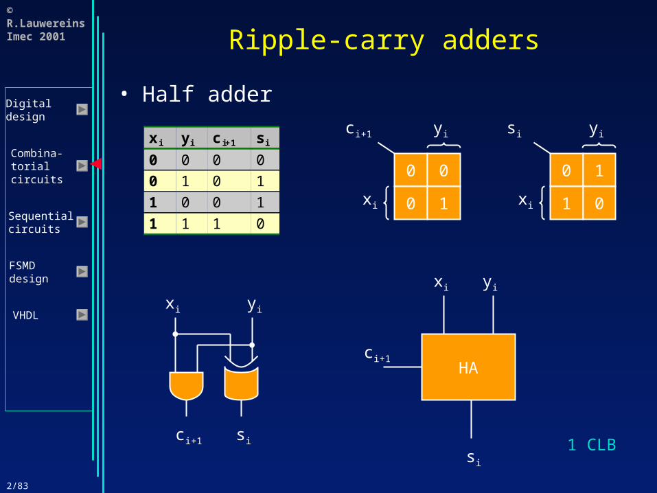
Ripple-carry adders
• Half adder
xi yi c i+1 si
0 0 0 00 1 0 1
1 0 0 1
1 1 1 0
0 0
0 1xi
yici+1
0 1
1 0xi
yisi
xi yi
ci+1 si
HA
xi yi
ci+1
si
1 CLB
2/84
© R.LauwereinsImec 2001
Digitaldesign
Combina-torialcircuits
Sequentialcircuits
FSMDdesign
VHDL
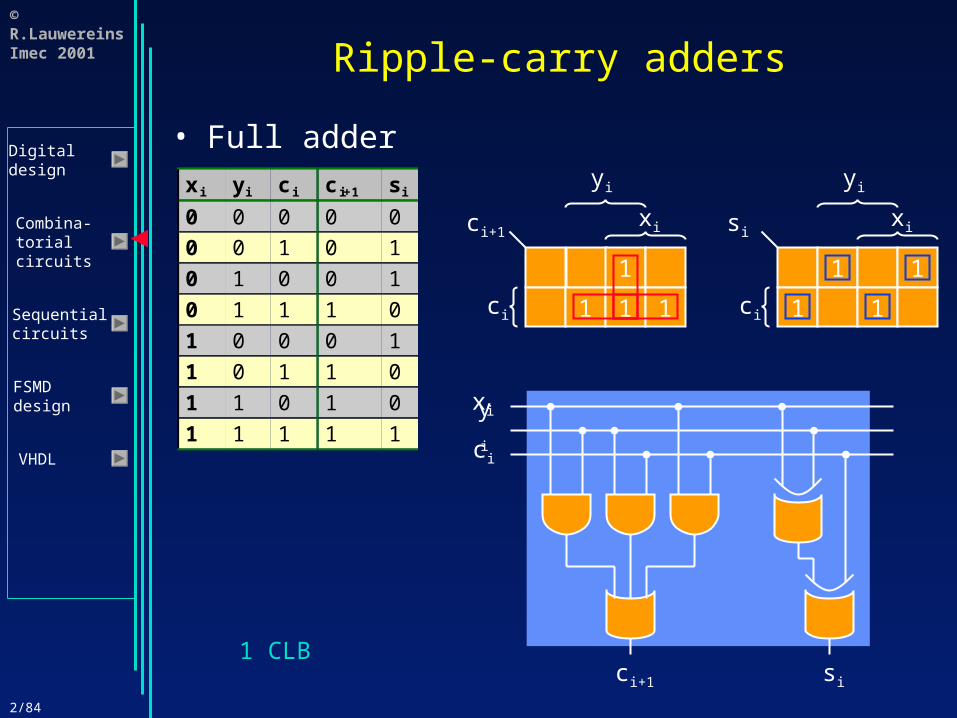
Ripple-carry adders
• Full adderxi yi c i c i+1 si
0 0 0 0 00 0 1 0 1
0 1 0 0 1
0 1 1 1 0
1 0 0 0 1
1 0 1 1 0
1 1 0 1 0
1 1 1 1 1
1
1 1 1ci
xi
yi
ci+1
1 1
1 1ci
xi
yi
si
xiyi
ci
ci+1 si
1 CLB
2/85
© R.LauwereinsImec 2001
Digitaldesign
Combina-torialcircuits
Sequentialcircuits
FSMDdesign
VHDL
Ripple-carry adders
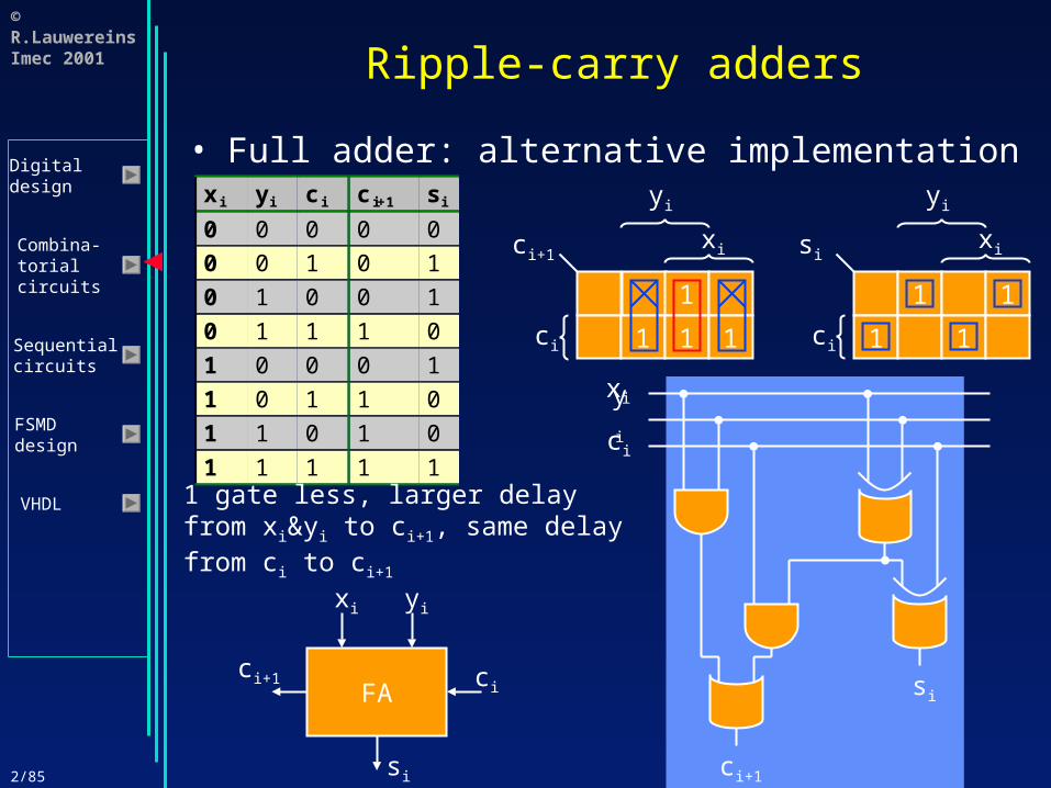
• Full adder: alternative implementationxi yi c i c i+1 si
0 0 0 0 00 0 1 0 1
0 1 0 0 1
0 1 1 1 0
1 0 0 0 1
1 0 1 1 0
1 1 0 1 0
1 1 1 1 1
yi
1 1
1 1ci
xi
yi
si
1
1 1 1ci
xici+1
xiyi
ci
ci+1
si
1 gate less, larger delayfrom xi&yi to ci+1, same delayfrom ci to ci+1
FA
xi yi
cici+1
si
2/86
© R.LauwereinsImec 2001
Digitaldesign
Combina-torialcircuits
Sequentialcircuits
FSMDdesign
VHDL
Ripple-carry adders
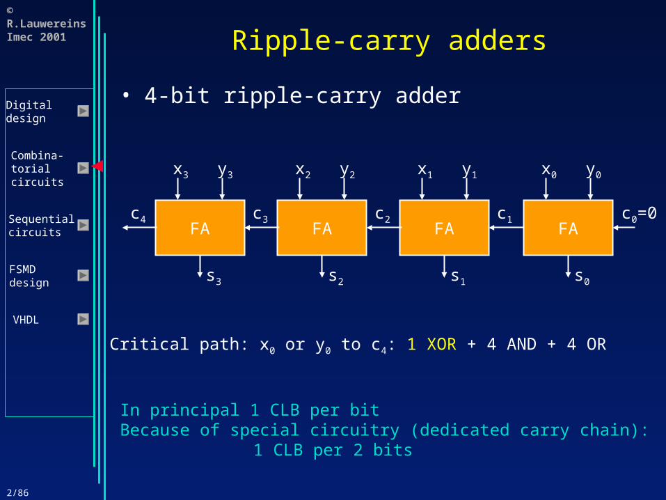
• 4-bit ripple-carry adder
FA
x0 y0
c0=0c1
s0
FA
x1 y1
c2
s1
FA
x2 y2
c3
s2
FA
x3 y3
c4
s3
Critical path: x0 or y0 to c4: 1 XOR + 4 AND + 4 OR
In principal 1 CLB per bitBecause of special circuitry (dedicated carry chain):
1 CLB per 2 bits
2/87
© R.LauwereinsImec 2001
Digitaldesign
Combina-torialcircuits
Sequentialcircuits
FSMDdesign
VHDL
Design of Combinatorial Circuits• Minimization of Boolean functions• Technology mapping• Correct timing behavior• Basic RTL building blocks
Ripple-carry adders Carry-look-ahead adders Adder/subtractors Multipliers Logic units Arithmetic-logic units Decoders Selectors Buses Priority encoders Magnitude comparators Shifters and rotators

2/88
© R.LauwereinsImec 2001
Digitaldesign
Combina-torialcircuits
Sequentialcircuits
FSMDdesign
VHDL
Carry-look-ahead adders
• Ripple-carry adder is slow because the critical path x0 to cn+1 is long
• Speed-up is possible by computing for example c4 directly (in principle in 2 layers of logic) from c0, x0…x3 en y0…y3. Hence the name Carry-look-ahead
• How is this done? See exercises and course book
4-bit CLA ci
xi…i+3 yi…i+3
si…i+3
ci+4
2/89
© R.LauwereinsImec 2001
Digitaldesign
Combina-torialcircuits
Sequentialcircuits
FSMDdesign
VHDL
Design of Combinatorial Circuits• Minimization of Boolean functions• Technology mapping• Correct timing behavior• Basic RTL building blocks
Ripple-carry adders Carry-look-ahead adders Adder/subtractors Multipliers Logic units Arithmetic-logic units Decoders Selectors Buses Priority encoders Magnitude comparators Shifters and rotators

2/90
© R.LauwereinsImec 2001
Digitaldesign
Combina-torialcircuits
Sequentialcircuits
FSMDdesign
VHDL
Adder-subtractors
FA
x0 y0
c0c1
f0
FA
x1 y1
c2
f1
FA
x2 y2
c3
f2
FA
x3 y3
c4
f3
S
S Function Note
0 X+Y Addition
1 X-Y =X+Y *=X+Y ’+1 SubtractionAdder/
subtractor
X Y
F
SCout
overflow Only for 2-complement!!!

2/91
© R.LauwereinsImec 2001
Digitaldesign
Combina-torialcircuits
Sequentialcircuits
FSMDdesign
VHDL
Design of Combinatorial Circuits• Minimization of Boolean functions• Technology mapping• Correct timing behavior• Basic RTL building blocks
Ripple-carry adders Carry-look-ahead adders Adder/subtractors Multipliers Logic units Arithmetic-logic units Decoders Selectors Buses Priority encoders Magnitude comparators Shifters and rotators

2/92
© R.LauwereinsImec 2001
Digitaldesign
Combina-torialcircuits
Sequentialcircuits
FSMDdesign
VHDL
Multipliers
• A 1-bit by 1-bit multiplier:C = B • A
b0
a0
a0b0
b0 a0 c0=a0.b0
0 0 0
b0 a0 c0=a0.b0
0 0 0
0 1 0
b0 a0 c0=a0.b0
0 0 0
0 1 0
1 0 0
b0 a0 c0=a0.b0
0 0 0
0 1 0
1 0 0
1 1 1
b0 a0 c0=a0.b0
0 0 0
0 1 0
1 0 0
1 1 1
A 1-bit by 1-bit multiplier is hence an AND gate
a0 b0
c0
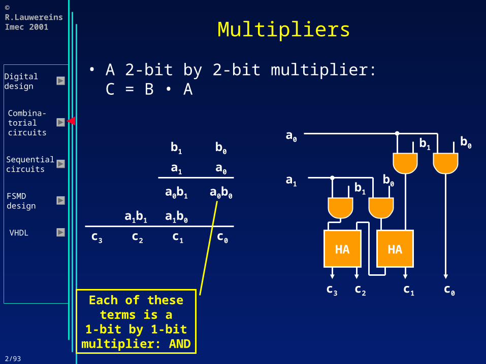
2/93
© R.LauwereinsImec 2001
Digitaldesign
Combina-torialcircuits
Sequentialcircuits
FSMDdesign
VHDL
Multipliers
• A 2-bit by 2-bit multiplier:C = B • A
a0b0
b0
a0
b1
a1
a0b1
a1b0a1b1
c0c1c2c3
Each of theseterms is a
1-bit by 1-bitmultiplier: AND
b0b1
a0
b0b1
a1
HAHA
c0c1c2c3

2/94
© R.LauwereinsImec 2001
Digitaldesign
Combina-torialcircuits
Sequentialcircuits
FSMDdesign
VHDL
Multipliers
• A 4-bit by 3-bit multiplier: cost=O(n2)b0
b1
a0b2b3
b0b1
a1 b2b3
4-bit adder
0
b0b1
a2 b2b3
4-bit adder
c0c1c2c3c4c5c6
s0s1s2s3cout
s0s1s2s3cout
2/95
© R.LauwereinsImec 2001
Digitaldesign
Combina-torialcircuits
Sequentialcircuits
FSMDdesign
VHDL
Design of Combinatorial Circuits• Minimization of Boolean functions• Technology mapping• Correct timing behavior• Basic RTL building blocks
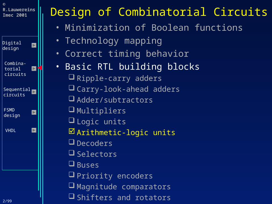
Ripple-carry adders Carry-look-ahead adders Adder/subtractors Multipliers Logic units Arithmetic-logic units Decoders Selectors Buses Priority encoders Magnitude comparators Shifters and rotators
2/96
© R.LauwereinsImec 2001
Digitaldesign
Combina-torialcircuits
Sequentialcircuits
FSMDdesign
VHDL
Logic units
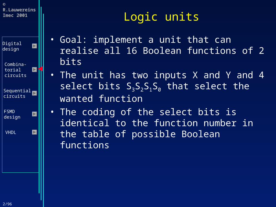
• Goal: implement a unit that can realise all 16 Boolean functions of 2 bits
• The unit has two inputs X and Y and 4 select bits S3S2S1S0 that select the wanted function
• The coding of the select bits is identical to the function number in the table of possible Boolean functions
2/97
© R.LauwereinsImec 2001
Digitaldesign
Combina-torialcircuits
Sequentialcircuits
FSMDdesign
VHDL
Logic units
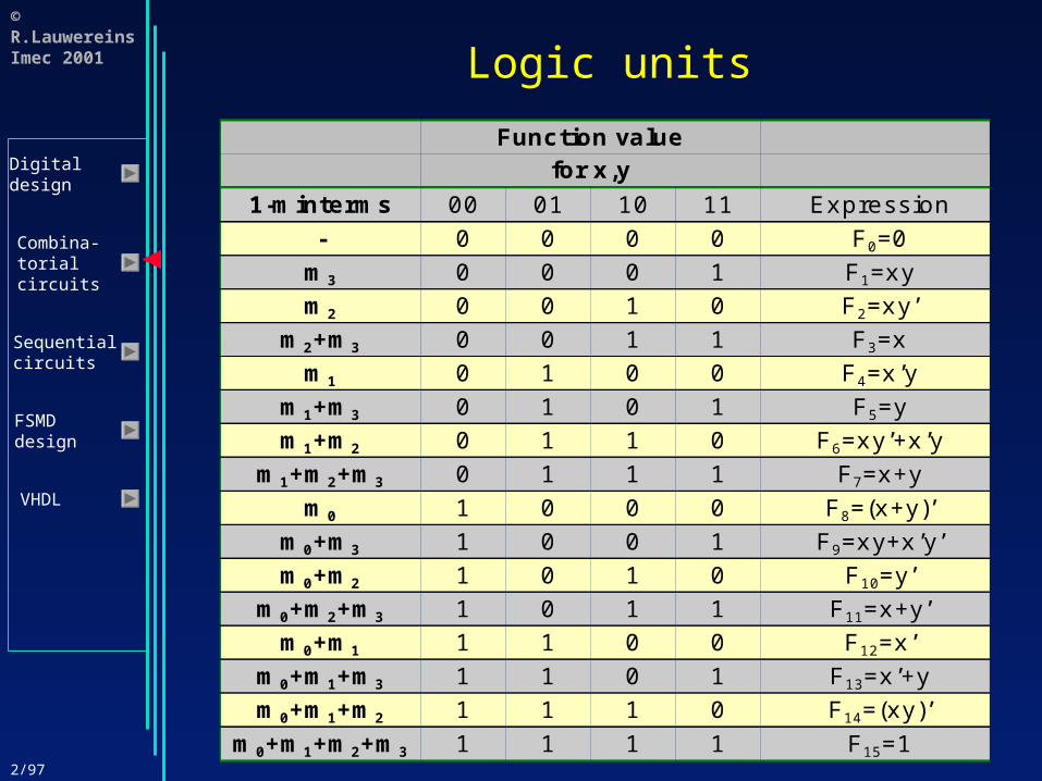
Function valuefor x,y
1-minterms 00 01 10 11 Expression
- 0 0 0 0 F0=0m3 0 0 0 1 F1=xym2 0 0 1 0 F2=xy’
m2+m3 0 0 1 1 F3=xm1 0 1 0 0 F4=x’y
m1+m3 0 1 0 1 F5=ym1+m2 0 1 1 0 F6=xy’+x’y
m1+m2+m3 0 1 1 1 F7=x+y
m0 1 0 0 0 F8=(x+y)’m0+m3 1 0 0 1 F9=xy+x’y’m0+m2 1 0 1 0 F10=y’
m0+m2+m3 1 0 1 1 F11=x+y’m0+m1 1 1 0 0 F12=x’
m0+m1+m3 1 1 0 1 F13=x’+ym0+m1+m2 1 1 1 0 F14=(xy)’
m0+m1+m2+m3 1 1 1 1 F15=1

2/98
© R.LauwereinsImec 2001
Digitaldesign
Combina-torialcircuits
Sequentialcircuits
FSMDdesign
VHDL
Logic units
S0S1S2S3
xiyi
fi
LU
xi yi
fi
S0..3
2/99
© R.LauwereinsImec 2001
Digitaldesign
Combina-torialcircuits
Sequentialcircuits
FSMDdesign
VHDL
Design of Combinatorial Circuits• Minimization of Boolean functions• Technology mapping• Correct timing behavior• Basic RTL building blocks
Ripple-carry adders Carry-look-ahead adders Adder/subtractors Multipliers Logic units Arithmetic-logic units Decoders Selectors Buses Priority encoders Magnitude comparators Shifters and rotators

2/100
© R.LauwereinsImec 2001
Digitaldesign
Combina-torialcircuits
Sequentialcircuits
FSMDdesign
VHDL
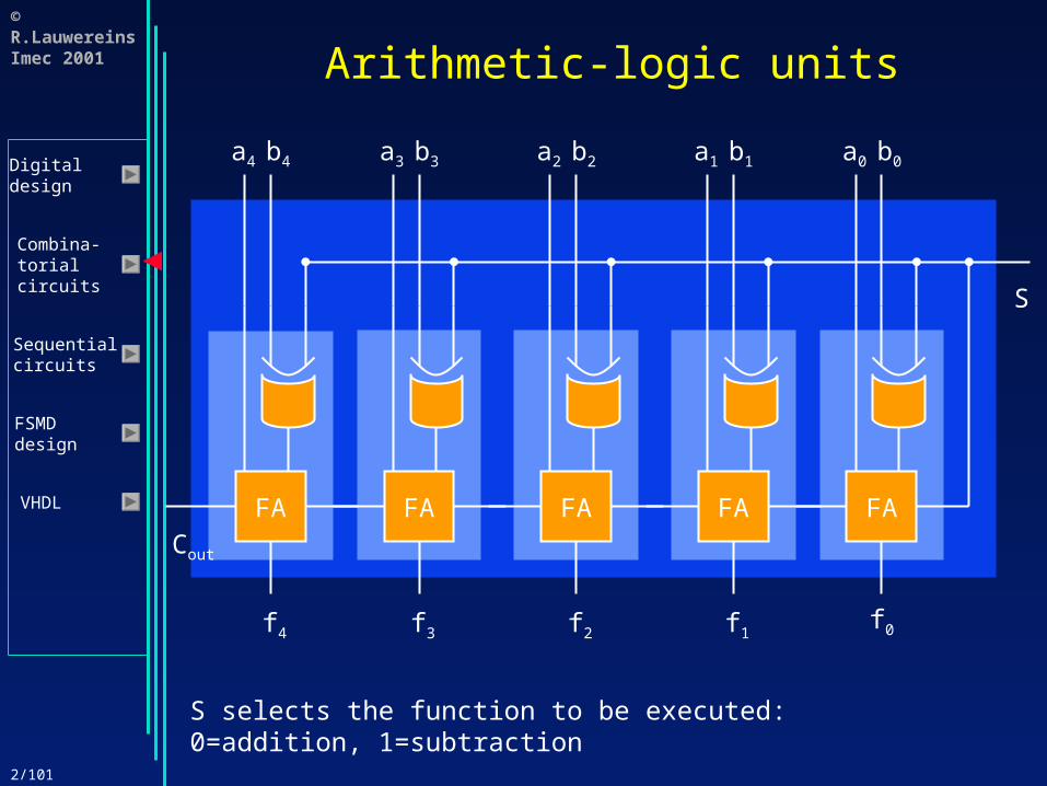
Arithmetic-logic units
• Goal: build a unit that realises 4 arithmetic operations (addition, subtraction, increment and decrement) and 4 logic operations (AND, OR, INV, identity)
• Realisation principle: use an adder in front of which we place a modifier circuit (Arithmetic-Logic Extender)
• This principle has already been applied for the 2-complement adder/subtractor: this was an adder in front of which we placed an exor circuit to allow for subtraction
2/101
© R.LauwereinsImec 2001
Digitaldesign
Combina-torialcircuits
Sequentialcircuits
FSMDdesign
VHDL
Arithmetic-logic units
FAFAFAFAFA
a0 b0a1 b1a2 b2a3 b3a4 b4
f0f1f2f3f4
S
Cout
S selects the function to be executed: 0=addition, 1=subtraction
2/102
© R.LauwereinsImec 2001
Digitaldesign
Combina-torialcircuits
Sequentialcircuits
FSMDdesign
VHDL
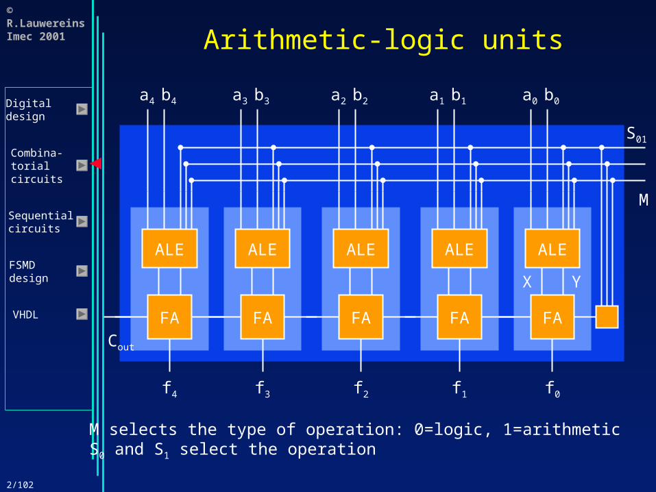
Arithmetic-logic units
M
M selects the type of operation: 0=logic, 1=arithmeticS0 and S1 select the operation
FA
a0 b0
f0
ALE
FA
a1 b1
f1
ALE
FA
a2 b2
f2
ALE
FA
a3 b3
f3
ALE
FA
a4 b4
f4
ALE
Cout
S01
X Y

2/103
© R.LauwereinsImec 2001
Digitaldesign
Combina-torialcircuits
Sequentialcircuits
FSMDdesign
VHDL
Arithmetic-logic units
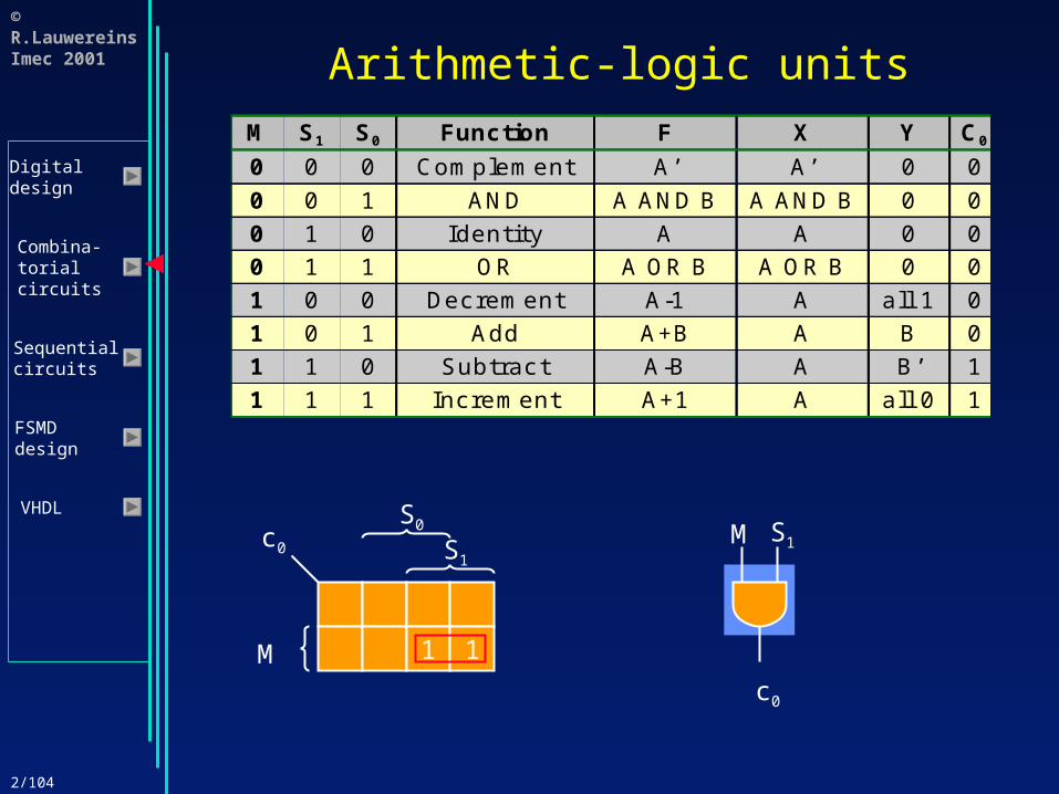
M S1 S0 Function F X Y C0
0 0 0 Complement A’ A’ 0 0
M S1 S0 Function F X Y C0
0 0 0 Complement A’ A’ 0 0
0 0 1 AND A AND B A AND B 0 0
M S1 S0 Function F X Y C0
0 0 0 Complement A’ A’ 0 0
0 0 1 AND A AND B A AND B 0 00 1 0 Identity A A 0 0
M S1 S0 Function F X Y C0
0 0 0 Complement A’ A’ 0 0
0 0 1 AND A AND B A AND B 0 00 1 0 Identity A A 0 00 1 1 OR A OR B A OR B 0 0
M S1 S0 Function F X Y C0
0 0 0 Complement A’ A’ 0 0
0 0 1 AND A AND B A AND B 0 00 1 0 Identity A A 0 00 1 1 OR A OR B A OR B 0 01 0 0 Decrement A-1 A all 1 0
M S1 S0 Function F X Y C0
0 0 0 Complement A’ A’ 0 0
0 0 1 AND A AND B A AND B 0 00 1 0 Identity A A 0 00 1 1 OR A OR B A OR B 0 01 0 0 Decrement A-1 A all 1 01 0 1 Add A+B A B 0
M S1 S0 Function F X Y C0
0 0 0 Complement A’ A’ 0 0
0 0 1 AND A AND B A AND B 0 00 1 0 Identity A A 0 00 1 1 OR A OR B A OR B 0 01 0 0 Decrement A-1 A all 1 01 0 1 Add A+B A B 01 1 0 Subtract A-B A B’ 1
M S1 S0 Function F X Y C0
0 0 0 Complement A’ A’ 0 0
0 0 1 AND A AND B A AND B 0 00 1 0 Identity A A 0 00 1 1 OR A OR B A OR B 0 01 0 0 Decrement A-1 A all 1 01 0 1 Add A+B A B 01 1 0 Subtract A-B A B’ 11 1 1 Increment A+1 A all 0 1
2/104
© R.LauwereinsImec 2001
Digitaldesign
Combina-torialcircuits
Sequentialcircuits
FSMDdesign
VHDL
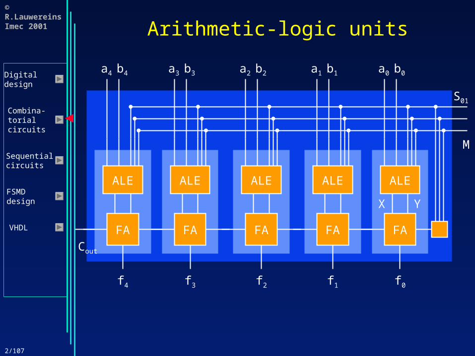
Arithmetic-logic unitsM S1 S0 Function F X Y C0
0 0 0 Complement A’ A’ 0 0
0 0 1 AND A AND B A AND B 0 00 1 0 Identity A A 0 00 1 1 OR A OR B A OR B 0 01 0 0 Decrement A-1 A all 1 01 0 1 Add A+B A B 01 1 0 Subtract A-B A B’ 11 1 1 Increment A+1 A all 0 1
1 1M
S1
S0c0
M S1
c0
2/105
© R.LauwereinsImec 2001
Digitaldesign
Combina-torialcircuits
Sequentialcircuits
FSMDdesign
VHDL
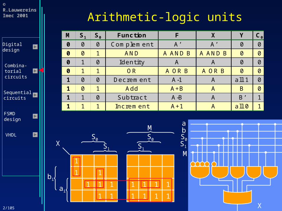
Arithmetic-logic unitsM S1 S0 Function F X Y C0
0 0 0 Complement A’ A’ 0 0
0 0 1 AND A AND B A AND B 0 00 1 0 Identity A A 0 00 1 1 OR A OR B A OR B 0 01 0 0 Decrement A-1 A all 1 01 0 1 Add A+B A B 01 1 0 Subtract A-B A B’ 11 1 1 Increment A+1 A all 0 1
1
1 1
M
S1
S0X
1 1 1
1 1ai
bi
1 1 1 1
1 1 1 1
S1
S0
ba
S0S1
M
X
2/106
© R.LauwereinsImec 2001
Digitaldesign
Combina-torialcircuits
Sequentialcircuits
FSMDdesign
VHDL
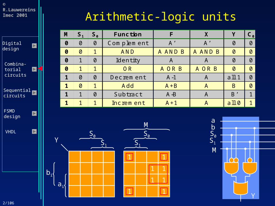
Arithmetic-logic unitsM S1 S0 Function F X Y C0
0 0 0 Complement A’ A’ 0 0
0 0 1 AND A AND B A AND B 0 00 1 0 Identity A A 0 00 1 1 OR A OR B A OR B 0 01 0 0 Decrement A-1 A all 1 01 0 1 Add A+B A B 01 1 0 Subtract A-B A B’ 11 1 1 Increment A+1 A all 0 1
bi
M
S1
S0Y
ai
1 1
1 1
1 1
1 1
S1
S0
ba
S0S1
M
Y
2/107
© R.LauwereinsImec 2001
Digitaldesign
Combina-torialcircuits
Sequentialcircuits
FSMDdesign
VHDL
Arithmetic-logic units
M
FA
a0 b0
f0
ALE
FA
a1 b1
f1
ALE
FA
a2 b2
f2
ALE
FA
a3 b3
f3
ALE
FA
a4 b4
f4
ALE
Cout
S01
X Y
2/108
© R.LauwereinsImec 2001
Digitaldesign
Combina-torialcircuits
Sequentialcircuits
FSMDdesign
VHDL
Design of Combinatorial Circuits• Minimization of Boolean functions• Technology mapping• Correct timing behavior• Basic RTL building blocks
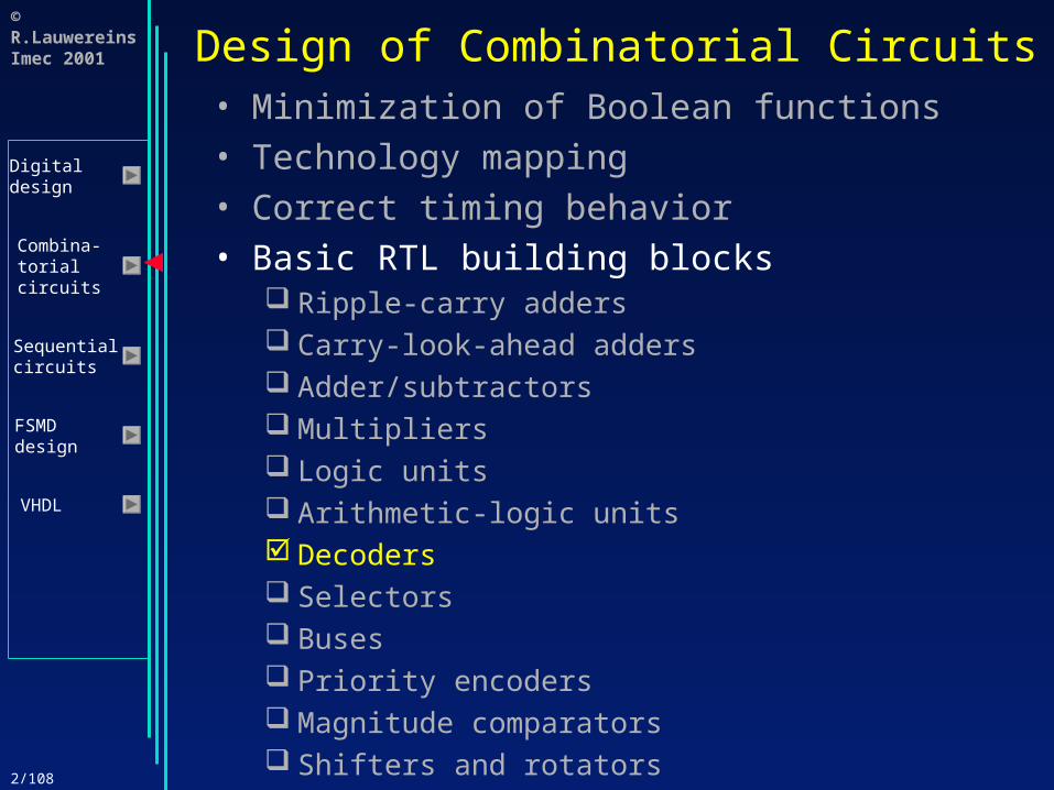
Ripple-carry adders Carry-look-ahead adders Adder/subtractors Multipliers Logic units Arithmetic-logic units Decoders Selectors Buses Priority encoders Magnitude comparators Shifters and rotators
2/109
© R.LauwereinsImec 2001
Digitaldesign
Combina-torialcircuits
Sequentialcircuits
FSMDdesign
VHDL
Decoders
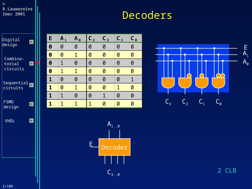
E A1 A0 C3 C2 C1 C0
0 0 0 0 0 0 00 0 1 0 0 0 0
0 1 0 0 0 0 0
0 1 1 0 0 0 0
1 0 0 0 0 0 1
1 0 1 0 0 1 0
1 1 0 0 1 0 0
1 1 1 1 0 0 0
EA1
A0
C3 C2 C1 C0
Decoder
C3..0
A1..0
E
2 CLB
2/110
© R.LauwereinsImec 2001
Digitaldesign
Combina-torialcircuits
Sequentialcircuits
FSMDdesign
VHDL
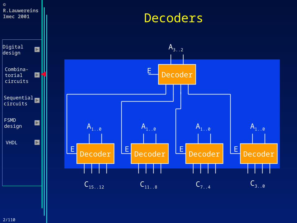
Decoders
Decoder
C3..0
A1..0
EDecoder
C7..4
A1..0
EDecoder
C11..8
A1..0
EDecoder
C15..12
A1..0
E
Decoder
A3..2
E
2/111
© R.LauwereinsImec 2001
Digitaldesign
Combina-torialcircuits
Sequentialcircuits
FSMDdesign
VHDL
Design of Combinatorial Circuits• Minimization of Boolean functions• Technology mapping• Correct timing behavior• Basic RTL building blocks
Ripple-carry adders Carry-look-ahead adders Adder/subtractors Multipliers Logic units Arithmetic-logic units Decoders Selectors Buses Priority encoders Magnitude comparators Shifters and rotators
2/112
© R.LauwereinsImec 2001
Digitaldesign
Combina-torialcircuits
Sequentialcircuits
FSMDdesign
VHDL
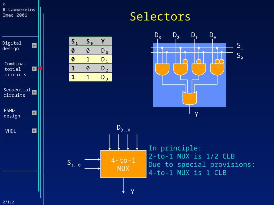
Selectors
S1 S0 Y
0 0 D0
0 1 D1
1 0 D2
1 1 D3
D3 D2 D1 D0
S1
S0
Y
4-to-1MUX
D3..0
S1..0
Y
In principle:2-to-1 MUX is 1/2 CLBDue to special provisions:4-to-1 MUX is 1 CLB
2/113
© R.LauwereinsImec 2001
Digitaldesign
Combina-torialcircuits
Sequentialcircuits
FSMDdesign
VHDL
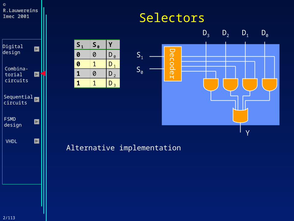
Selectors
S1 S0 Y
0 0 D0
0 1 D1
1 0 D2
1 1 D3
D3 D2 D1 D0
Y
Deco
der
S1
S0
Alternative implementation

2/114
© R.LauwereinsImec 2001
Digitaldesign
Combina-torialcircuits
Sequentialcircuits
FSMDdesign
VHDL
Selectors
4-to-1selector
S3..2
4-to-1selector
D7..4
S1..0
4-to-1selector
D11..8
S1..0
4-to-1selector
D15..12
S1..0
4-to-1selector
D3..0
S1..0
Y

2/115
© R.LauwereinsImec 2001
Digitaldesign
Combina-torialcircuits
Sequentialcircuits
FSMDdesign
VHDL
Design of Combinatorial Circuits• Minimization of Boolean functions• Technology mapping• Correct timing behavior• Basic RTL building blocks
Ripple-carry adders Carry-look-ahead adders Adder/subtractors Multipliers Logic units Arithmetic-logic units Decoders Selectors Buses Priority encoders Magnitude comparators Shifters and rotators

2/116
© R.LauwereinsImec 2001
Digitaldesign
Combina-torialcircuits
Sequentialcircuits
FSMDdesign
VHDL
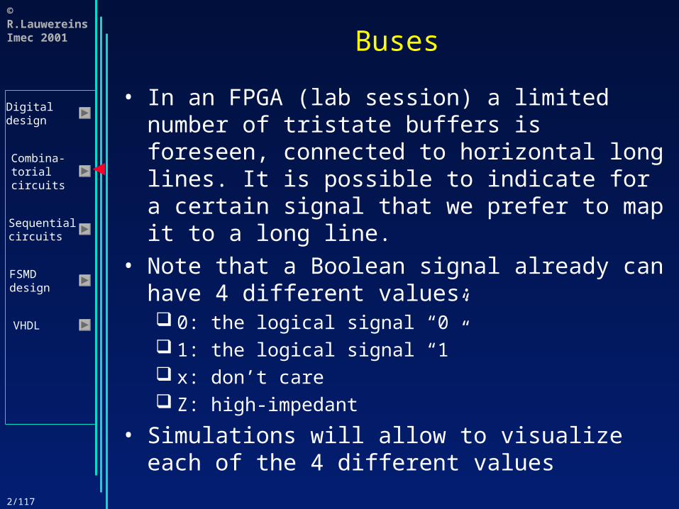
Buses
• Problem with high fan-in MUX: fan-in OR gate too big all inputs have to be routed to 1 central location:
substantial routing delay and difficult routing
• Solution: bus with tristate drivers
Deco
der
D3 D2 D1 D0 S1 S0
E Y
0 Z1 D
Y
2/117
© R.LauwereinsImec 2001
Digitaldesign
Combina-torialcircuits
Sequentialcircuits
FSMDdesign
VHDL
Buses
• In an FPGA (lab session) a limited number of tristate buffers is foreseen, connected to horizontal long lines. It is possible to indicate for a certain signal that we prefer to map it to a long line.
• Note that a Boolean signal already can have 4 different values: 0: the logical signal “0” 1: the logical signal “1” x: don’t care Z: high-impedant
• Simulations will allow to visualize each of the 4 different values
2/118
© R.LauwereinsImec 2001
Digitaldesign
Combina-torialcircuits
Sequentialcircuits
FSMDdesign
VHDL
Design of Combinatorial Circuits• Minimization of Boolean functions• Technology mapping• Correct timing behavior• Basic RTL building blocks
Ripple-carry adders Carry-look-ahead adders Adder/subtractors Multipliers Logic units Arithmetic-logic units Decoders Selectors Buses Priority encoders Magnitude comparators Shifters and rotators

2/119
© R.LauwereinsImec 2001
Digitaldesign
Combina-torialcircuits
Sequentialcircuits
FSMDdesign
VHDL
Priority encoders
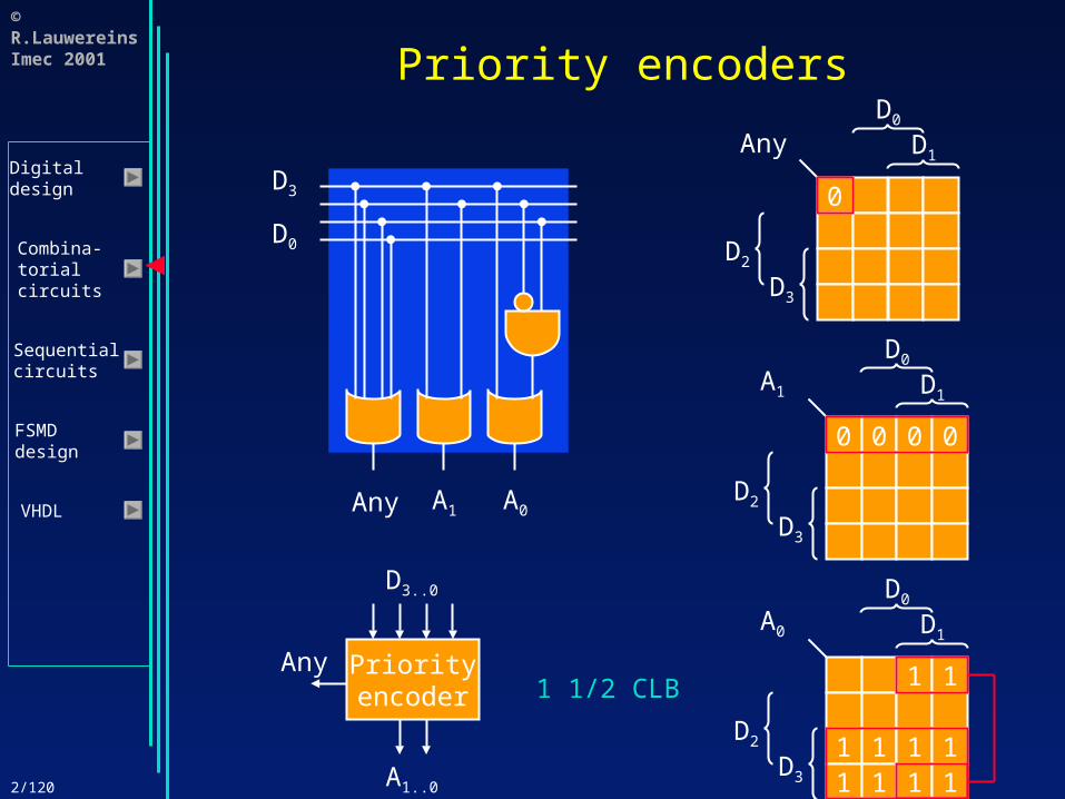
D3 D2 D1 D0 A1 A0 Any
0 0 0 0 0 0 0
D3 D2 D1 D0 A1 A0 Any
0 0 0 0 0 0 0
0 0 0 1 0 0 1
D3 D2 D1 D0 A1 A0 Any
0 0 0 0 0 0 0
0 0 0 1 0 0 1
0 0 1 0 0 1 1
0 0 1 1 0 1 1
D3 D2 D1 D0 A1 A0 Any
0 0 0 0 0 0 0
0 0 0 1 0 0 1
0 0 1 0 0 1 1
0 0 1 1 0 1 1
0 1 0 0 1 0 1
0 1 0 1 1 0 1
0 1 1 0 1 0 1
0 1 1 1 1 0 1
D3 D2 D1 D0 A1 A0 Any
0 0 0 0 0 0 0
0 0 0 1 0 0 1
0 0 1 0 0 1 1
0 0 1 1 0 1 1
0 1 0 0 1 0 1
0 1 0 1 1 0 1
0 1 1 0 1 0 1
0 1 1 1 1 0 1
1 0 0 0 1 1 1
1 0 0 1 1 1 1
1 0 1 0 1 1 1
1 0 1 1 1 1 1
1 1 0 0 1 1 1
1 1 0 1 1 1 1
1 1 1 0 1 1 1
1 1 1 1 1 1 1
D3 D2 D1 D0 A1 A0 Any
0 0 0 0 0 0 00 0 0 1 0 0 1
0 0 1 0 0 1 1
0 0 1 1 0 1 1
0 1 0 0 1 0 1
0 1 0 1 1 0 1
0 1 1 0 1 0 1
0 1 1 1 1 0 1
1 0 0 0 1 1 1
1 0 0 1 1 1 1
1 0 1 0 1 1 1
1 0 1 1 1 1 1
1 1 0 0 1 1 1
1 1 0 1 1 1 1
1 1 1 0 1 1 1
1 1 1 1 1 1 1
0
D2
D3
D1
D0
Any
0 0 0 0
D2
D3
D1
D0
A1
1 1
1 1 1 11 1 1 1
D2
D3
D1
D0
A0
2/120
© R.LauwereinsImec 2001
Digitaldesign
Combina-torialcircuits
Sequentialcircuits
FSMDdesign
VHDL
Priority encoders
0
D2
D3
D1
D0
Any
0 0 0 0
D2
D3
D1
D0
A1
1 1
1 1 1 11 1 1 1
D2
D3
D1
D0
A0
D3
D0
Any A1 A0
Priorityencoder
D3..0
A1..0
Any1 1/2 CLB
2/121
© R.LauwereinsImec 2001
Digitaldesign
Combina-torialcircuits
Sequentialcircuits
FSMDdesign
VHDL
Priority encoders
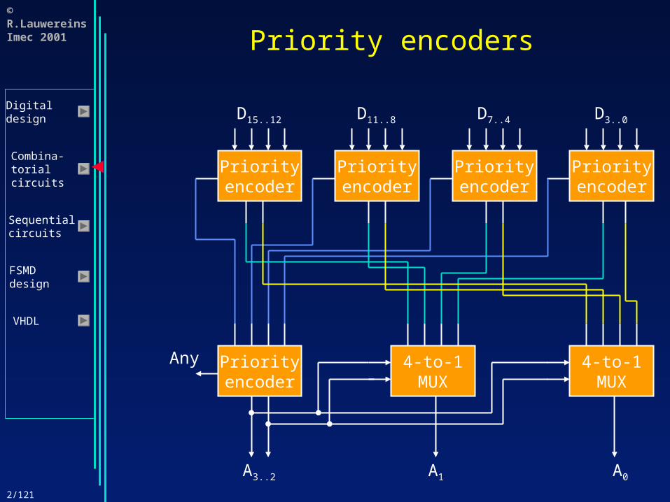
Priorityencoder
D3..0
Priorityencoder
D7..4
Priorityencoder
D11..8
Priorityencoder
D15..12
Priorityencoder
A3..2
Any 4-to-1MUX
A1
4-to-1MUX
A0

2/122
© R.LauwereinsImec 2001
Digitaldesign
Combina-torialcircuits
Sequentialcircuits
FSMDdesign
VHDL
Design of Combinatorial Circuits• Minimization of Boolean functions• Technology mapping• Correct timing behavior• Basic RTL building blocks
Ripple-carry adders Carry-look-ahead adders Adder/subtractors Multipliers Logic units Arithmetic-logic units Decoders Selectors Buses Priority encoders Magnitude comparators Shifters and rotators
2/123
© R.LauwereinsImec 2001
Digitaldesign
Combina-torialcircuits
Sequentialcircuits
FSMDdesign
VHDL
Magnitude comparators
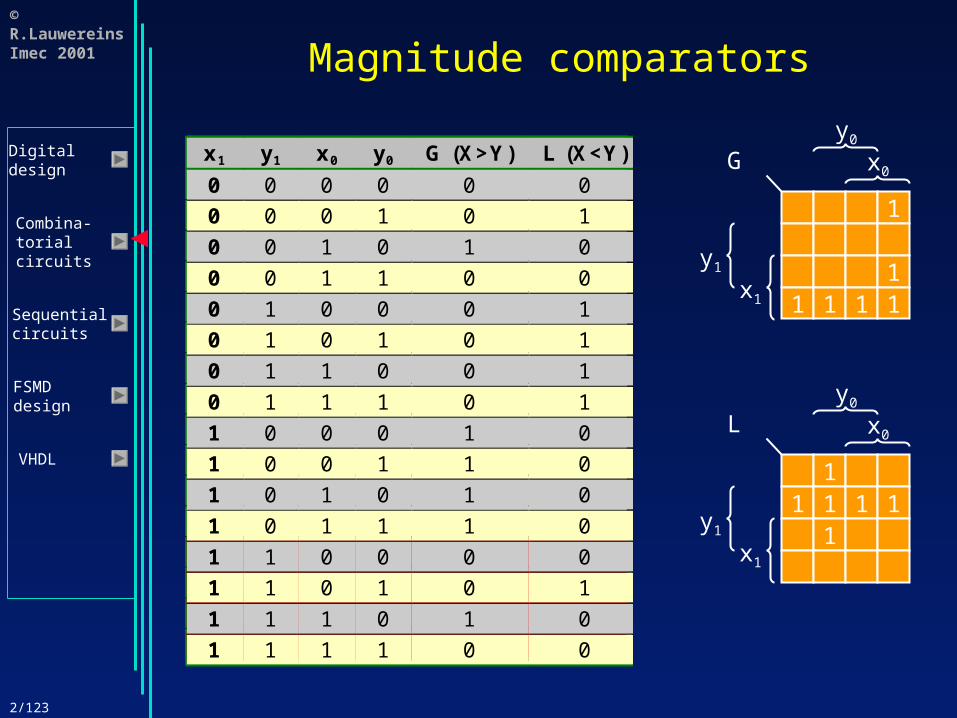
x1 y1 x0 y0 G (X>Y) L (X<Y)
0 0 0 0 0 0
0 0 0 1 0 1
0 0 1 0 1 0
0 0 1 1 0 0
x1 y1 x0 y0 G (X>Y) L (X<Y)
0 0 0 0 0 00 0 0 1 0 1
0 0 1 0 1 0
0 0 1 1 0 0
0 1 0 0 0 1
0 1 0 1 0 1
0 1 1 0 0 1
0 1 1 1 0 1
x1 y1 x0 y0 G (X>Y) L (X<Y)
0 0 0 0 0 00 0 0 1 0 1
0 0 1 0 1 0
0 0 1 1 0 0
0 1 0 0 0 1
0 1 0 1 0 1
0 1 1 0 0 1
0 1 1 1 0 1
1 0 0 0 1 0
1 0 0 1 1 0
1 0 1 0 1 0
1 0 1 1 1 0
x1 y1 x0 y0 G (X>Y) L (X<Y)
0 0 0 0 0 00 0 0 1 0 1
0 0 1 0 1 0
0 0 1 1 0 0
0 1 0 0 0 1
0 1 0 1 0 1
0 1 1 0 0 1
0 1 1 1 0 1
1 0 0 0 1 0
1 0 0 1 1 0
1 0 1 0 1 0
1 0 1 1 1 0
1 1 0 0 0 0
1 1 0 1 0 1
1 1 1 0 1 0
1 1 1 1 0 0
x1 y1 x0 y0 G (X>Y) L (X<Y)
0 0 0 0 0 00 0 0 1 0 1
0 0 1 0 1 0
0 0 1 1 0 0
0 1 0 0 0 1
0 1 0 1 0 1
0 1 1 0 0 1
0 1 1 1 0 1
1 0 0 0 1 0
1 0 0 1 1 0
1 0 1 0 1 0
1 0 1 1 1 0
1 1 0 0 0 0
1 1 0 1 0 1
1 1 1 0 1 0
1 1 1 1 0 0
1
11 1 1 1
y1
x1
x0
y0
G
11 1 1 1
1y1
x1
x0
y0
L
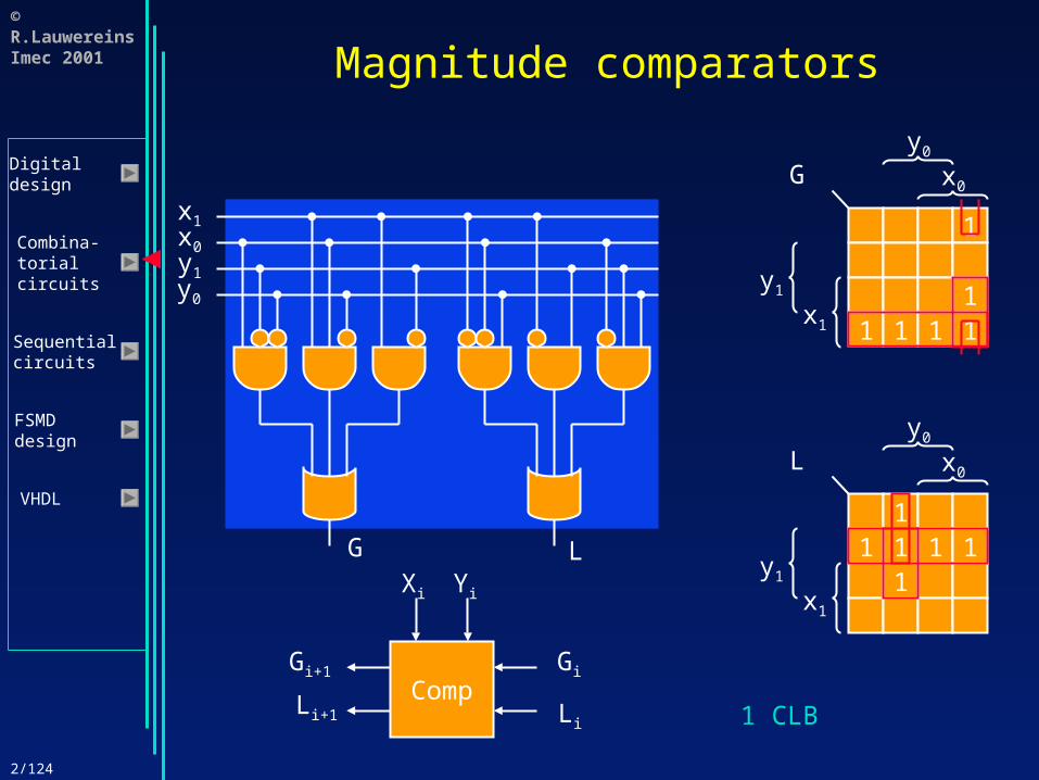
2/124
© R.LauwereinsImec 2001
Digitaldesign
Combina-torialcircuits
Sequentialcircuits
FSMDdesign
VHDL
x1x0y1y0
Magnitude comparators
1
11 1 1 1
y1
x1
x0
y0
G
11 1 1 1
1y1
x1
x0
y0
L
G L
Comp
Xi Yi
Gi
Li
Gi+1
Li+1 1 CLB
2/125
© R.LauwereinsImec 2001
Digitaldesign
Combina-torialcircuits
Sequentialcircuits
FSMDdesign
VHDL
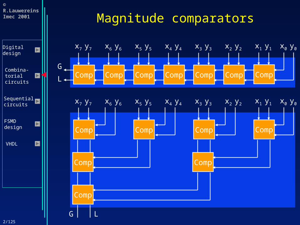
Magnitude comparators
Comp
x1 y1
Comp
x2 y2
Comp
x3 y3
Comp
x4 y4
Comp
x5 y5
Comp
x6 y6
Comp
x7 y7 x0 y0
G
L
Comp
x1 y1x2 y2
Comp
x3 y3x4 y4
Comp
x5 y5x6 y6
Comp
x7 y7 x0 y0
Comp
Comp
Comp
G L

2/126
© R.LauwereinsImec 2001
Digitaldesign
Combina-torialcircuits
Sequentialcircuits
FSMDdesign
VHDL
Magnitude comparators
• Simpler circuits are used for comparison with constants!!
y=1 when X=0
X
y
y=1 when X=255
y=1 when X>=64
X
y
y=1 when X<192
x7 x6
y
y=1 when X is even
x0
y
x7 x6
y
X is8 bits
2/127
© R.LauwereinsImec 2001
Digitaldesign
Combina-torialcircuits
Sequentialcircuits
FSMDdesign
VHDL
Design of Combinatorial Circuits• Minimization of Boolean functions• Technology mapping• Correct timing behavior• Basic RTL building blocks
Ripple-carry adders Carry-look-ahead adders Adder/subtractors Multipliers Logic units Arithmetic-logic units Decoders Selectors Buses Priority encoders Magnitude comparators Shifters and rotators
2/128
© R.LauwereinsImec 2001
Digitaldesign
Combina-torialcircuits
Sequentialcircuits
FSMDdesign
VHDL
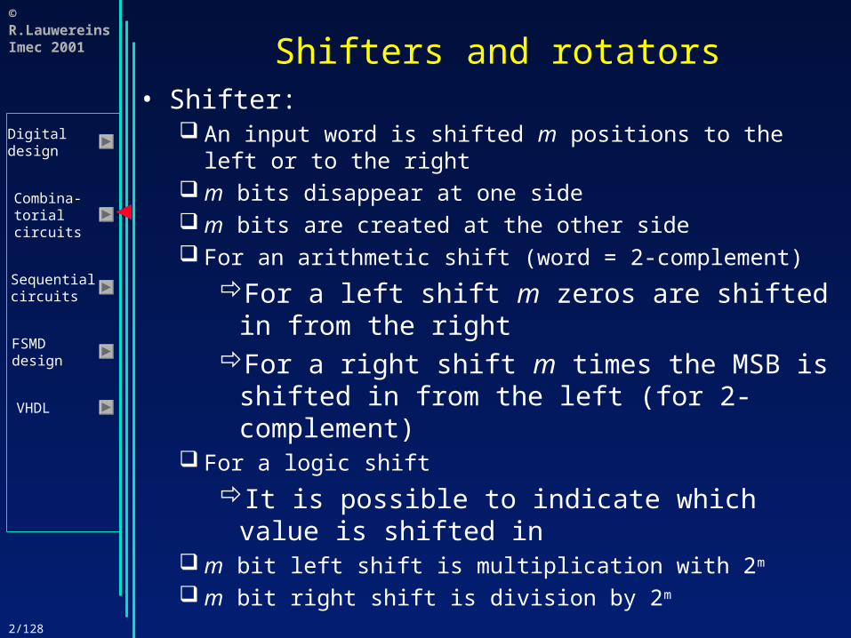
Shifters and rotators• Shifter:
An input word is shifted m positions to the left or to the right
m bits disappear at one side m bits are created at the other side For an arithmetic shift (word = 2-complement)
For a left shift m zeros are shifted in from the right
For a right shift m times the MSB is shifted in from the left (for 2-complement)
For a logic shift
It is possible to indicate which value is shifted in
m bit left shift is multiplication with 2m
m bit right shift is division by 2m
2/129
© R.LauwereinsImec 2001
Digitaldesign
Combina-torialcircuits
Sequentialcircuits
FSMDdesign
VHDL
Shifters and rotators
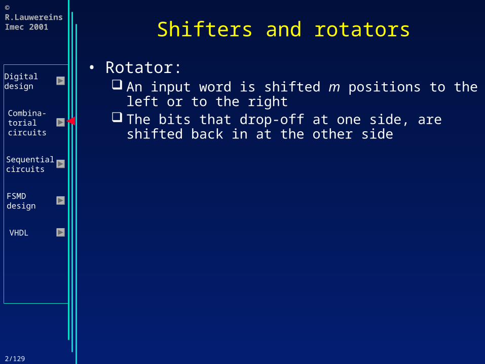
• Rotator: An input word is shifted m positions to the left or to
the right The bits that drop-off at one side, are shifted back
in at the other side

2/130
© R.LauwereinsImec 2001
Digitaldesign
Combina-torialcircuits
Sequentialcircuits
FSMDdesign
VHDL
Shifters and rotators
d0d1d2d3S2S1S0L-inR-in
4-to-1MUX
4-to-1MUX
4-to-1MUX
4-to-1MUX
MM
y3 y2 y1 y0
S2: 0=no shift,1=shift S1: 0=left,1=right S0: 0=shift,1=rotate
4-to-1MUX
4-to-1MUX
4-to-1MUX
4-to-1MUX
MM
y3 y2 y1 y0
S2: 0=no shift,1=shift S1: 0=left,1=right S0: 0=shift,1=rotate
4-to-1MUX
4-to-1MUX
4-to-1MUX
4-to-1MUX
MM
y3 y2 y1 y0
S2: 0=no shift,1=shift S1: 0=left,1=right S0: 0=shift,1=rotate
4-to-1MUX
4-to-1MUX
4-to-1MUX
4-to-1MUX
MM
y3 y2 y1 y0
S2: 0=no shift,1=shift S1: 0=left,1=right S0: 0=shift,1=rotate
4-to-1MUX
4-to-1MUX
4-to-1MUX
4-to-1MUX
MM
y3 y2 y1 y0
S2: 0=no shift,1=shift S1: 0=left,1=right S0: 0=shift,1=rotate
4-to-1MUX
4-to-1MUX
4-to-1MUX
4-to-1MUX
MM
y3 y2 y1 y0
S2: 0=no shift,1=shift S1: 0=left,1=right S0: 0=shift,1=rotate
2/131
© R.LauwereinsImec 2001
Digitaldesign
Combina-torialcircuits
Sequentialcircuits
FSMDdesign
VHDL
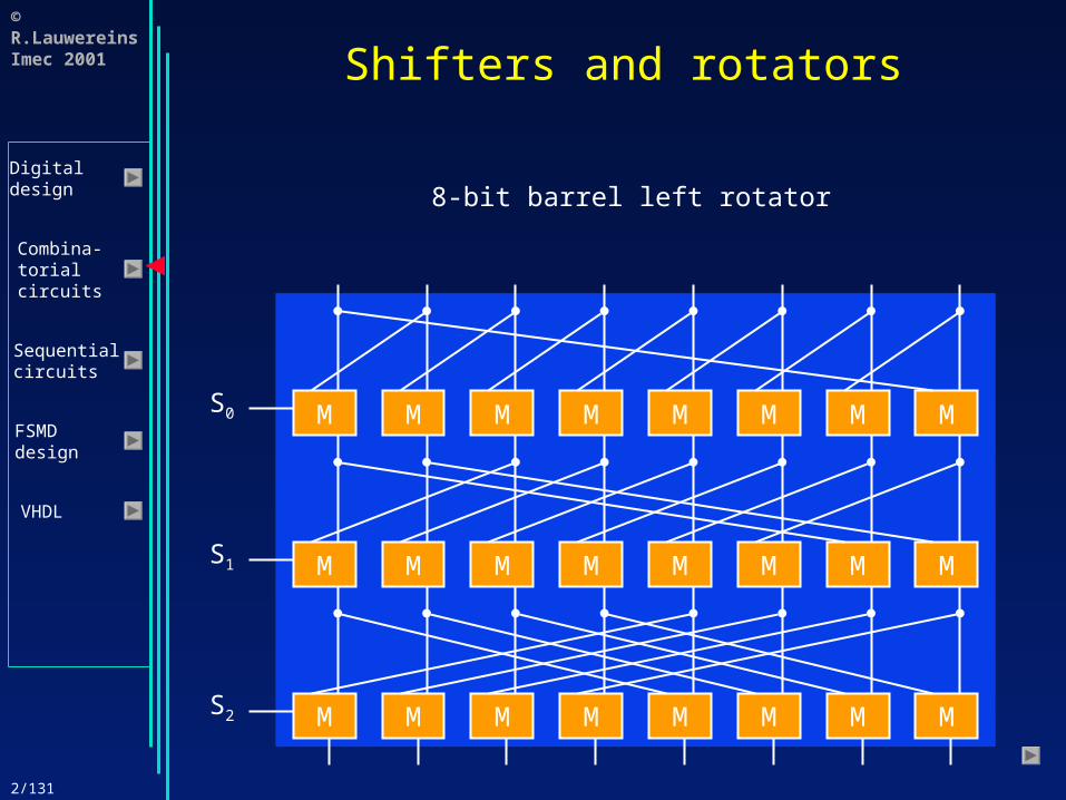
Shifters and rotators
MMMMMMMM
MMMMMMMM
MMMMMMMM
S0
S1
S2
8-bit barrel left rotator