elcodis.com - electronic components...
TRANSCRIPT
N e v e r s t o p t h i n k i n g .
HYB25D512[40/80/16]0B[C/T]HYB25D512[40/80/16]0B[E/F] 512Mbit Double Data Rate SDRAMDDR SDRAM
Data Sheet, Rev. 1.2, June 2004
Memory Products
查询HYB25D512160BC-5供应商查询HYB25D512160BC-5供应商
Downloaded from Elcodis.com electronic components distributor

Edition 2004-06
Published by Infineon Technologies AG,St.-Martin-Strasse 53,81669 München, Germany© Infineon Technologies AG 2004.All Rights Reserved.
Attention please!
The information herein is given to describe certain components and shall not be considered as a guarantee of characteristics.Terms of delivery and rights to technical change reserved.We hereby disclaim any and all warranties, including but not limited to warranties of non-infringement, regarding circuits, descriptions and charts stated herein.
Information
For further information on technology, delivery terms and conditions and prices please contact your nearest Infineon Technologies Office (www.infineon.com).
Warnings
Due to technical requirements components may contain dangerous substances. For information on the types in question please contact your nearest Infineon Technologies Office.Infineon Technologies Components may only be used in life-support devices or systems with the express written approval of Infineon Technologies, if a failure of such components can reasonably be expected to cause the failure of that life-support device or system, or to affect the safety or effectiveness of that device or system. Life support devices or systems are intended to be implanted in the human body, or to support and/or maintain and sustain and/or protect human life. If they fail, it is reasonable to assume that the health of the user or other persons may be endangered.
Downloaded from Elcodis.com electronic components distributor
N e v e r s t o p t h i n k i n g .
HYB25D512[40/80/16]0B[C/T]HYB25D512[40/80/16]0B[E/F] 512Mbit Double Data Rate SDRAMDDR SDRAM
Data Sheet, Rev. 1.2, June 2004
Memory Products
Downloaded from Elcodis.com electronic components distributor

Template: mp_a4_v1.0_2003-04-25.fm
HYB25D512[40/80/16]0B[C/T], HYB25D512[40/80/16]0B[E/F], Revision History: Rev. 1.2 2004-06
Previous Version: Rev. 1.1 2004-06
Page Subjects (major changes since last revision)
1 Editorial Change
67 Added AC Timing Table
We Listen to Your Comments
Any information within this document that you feel is wrong, unclear or missing at all?Your feedback will help us to continuously improve the quality of this document.Please send your proposal (including a reference to this document) to:
Downloaded from Elcodis.com electronic components distributor

Data Sheet 5 Rev. 1.2, 2004-06
HYB25D512[40/16/80]0B[E/F/C/T]512Mbit Double Data Rate SDRAM
1 Overview . . . . . . . . . . . . . . . . . . . . . . . . . . . . . . . . . . . . . . . . . . . . . . . . . . . . . . . . . . . . . . . . . . . . . . . 91.1 Features . . . . . . . . . . . . . . . . . . . . . . . . . . . . . . . . . . . . . . . . . . . . . . . . . . . . . . . . . . . . . . . . . . . . . . . . 91.2 Description . . . . . . . . . . . . . . . . . . . . . . . . . . . . . . . . . . . . . . . . . . . . . . . . . . . . . . . . . . . . . . . . . . . . . 10
2 Pin Configuration . . . . . . . . . . . . . . . . . . . . . . . . . . . . . . . . . . . . . . . . . . . . . . . . . . . . . . . . . . . . . . . 12
3 Functional Description . . . . . . . . . . . . . . . . . . . . . . . . . . . . . . . . . . . . . . . . . . . . . . . . . . . . . . . . . . . 223.1 Initialization . . . . . . . . . . . . . . . . . . . . . . . . . . . . . . . . . . . . . . . . . . . . . . . . . . . . . . . . . . . . . . . . . . . . . 223.2 Mode Register Definition . . . . . . . . . . . . . . . . . . . . . . . . . . . . . . . . . . . . . . . . . . . . . . . . . . . . . . . . . . 233.2.1 Burst Length . . . . . . . . . . . . . . . . . . . . . . . . . . . . . . . . . . . . . . . . . . . . . . . . . . . . . . . . . . . . . . . . . . 233.2.2 Burst Type . . . . . . . . . . . . . . . . . . . . . . . . . . . . . . . . . . . . . . . . . . . . . . . . . . . . . . . . . . . . . . . . . . . . 243.2.3 Read Latency . . . . . . . . . . . . . . . . . . . . . . . . . . . . . . . . . . . . . . . . . . . . . . . . . . . . . . . . . . . . . . . . . . 243.2.4 Operating Mode . . . . . . . . . . . . . . . . . . . . . . . . . . . . . . . . . . . . . . . . . . . . . . . . . . . . . . . . . . . . . . . . 253.3 Extended Mode Register . . . . . . . . . . . . . . . . . . . . . . . . . . . . . . . . . . . . . . . . . . . . . . . . . . . . . . . . . . 263.3.1 DLL Enable/Disable . . . . . . . . . . . . . . . . . . . . . . . . . . . . . . . . . . . . . . . . . . . . . . . . . . . . . . . . . . . . . 263.3.2 Output Drive Strength . . . . . . . . . . . . . . . . . . . . . . . . . . . . . . . . . . . . . . . . . . . . . . . . . . . . . . . . . . . 263.4 Commands . . . . . . . . . . . . . . . . . . . . . . . . . . . . . . . . . . . . . . . . . . . . . . . . . . . . . . . . . . . . . . . . . . . . . 273.5 Operations . . . . . . . . . . . . . . . . . . . . . . . . . . . . . . . . . . . . . . . . . . . . . . . . . . . . . . . . . . . . . . . . . . . . . 303.5.1 Bank/Row Activation . . . . . . . . . . . . . . . . . . . . . . . . . . . . . . . . . . . . . . . . . . . . . . . . . . . . . . . . . . . . 303.5.2 Reads . . . . . . . . . . . . . . . . . . . . . . . . . . . . . . . . . . . . . . . . . . . . . . . . . . . . . . . . . . . . . . . . . . . . . . . 313.5.3 Writes . . . . . . . . . . . . . . . . . . . . . . . . . . . . . . . . . . . . . . . . . . . . . . . . . . . . . . . . . . . . . . . . . . . . . . . . 403.5.4 Pre charge . . . . . . . . . . . . . . . . . . . . . . . . . . . . . . . . . . . . . . . . . . . . . . . . . . . . . . . . . . . . . . . . . . . . 543.5.5 Power-Down . . . . . . . . . . . . . . . . . . . . . . . . . . . . . . . . . . . . . . . . . . . . . . . . . . . . . . . . . . . . . . . . . . 553.5.6 Input Clock Frequency Change . . . . . . . . . . . . . . . . . . . . . . . . . . . . . . . . . . . . . . . . . . . . . . . . . . . . 593.6 Simplified State Diagram . . . . . . . . . . . . . . . . . . . . . . . . . . . . . . . . . . . . . . . . . . . . . . . . . . . . . . . . . . 60
4 Electrical Characteristics . . . . . . . . . . . . . . . . . . . . . . . . . . . . . . . . . . . . . . . . . . . . . . . . . . . . . . . . . 614.1 Operating Conditions . . . . . . . . . . . . . . . . . . . . . . . . . . . . . . . . . . . . . . . . . . . . . . . . . . . . . . . . . . . . . 61
5 Normal Strength Pull-down and Pull-up Characteristics . . . . . . . . . . . . . . . . . . . . . . . . . . . . . . . 635.1 Weak Strength Pull-down and Pull-up Characteristics . . . . . . . . . . . . . . . . . . . . . . . . . . . . . . . . . . . . 655.2 AC Characteristics . . . . . . . . . . . . . . . . . . . . . . . . . . . . . . . . . . . . . . . . . . . . . . . . . . . . . . . . . . . . . . . 675.2.1 IDD Current Measurement Conditions . . . . . . . . . . . . . . . . . . . . . . . . . . . . . . . . . . . . . . . . . . . . . . . 72
6 Timing Diagrams . . . . . . . . . . . . . . . . . . . . . . . . . . . . . . . . . . . . . . . . . . . . . . . . . . . . . . . . . . . . . . . . 73
7 System Characteristics for DDR SDRAMs . . . . . . . . . . . . . . . . . . . . . . . . . . . . . . . . . . . . . . . . . . . 85
8 Package Outlines . . . . . . . . . . . . . . . . . . . . . . . . . . . . . . . . . . . . . . . . . . . . . . . . . . . . . . . . . . . . . . . 88
Table of Contents
Downloaded from Elcodis.com electronic components distributor

Data Sheet 6 Rev. 1.2, 2004-06
HYB25D512[40/16/80]0B[E/F/C/T]512Mbit Double Data Rate SDRAM
Figure 1 Pin Configuration P-TFBGA-60-9 Top View, see the balls throught the package . . . . . . . . . . . . . 16Figure 2 Pin Configuration P-TSOPII-66-1 . . . . . . . . . . . . . . . . . . . . . . . . . . . . . . . . . . . . . . . . . . . . . . . . . . 17Figure 3 Block Diagram 512Mbit 128 Mbit ×4. . . . . . . . . . . . . . . . . . . . . . . . . . . . . . . . . . . . . . . . . . . . . . . . 19Figure 4 Block Diagram 512Mbit 64 Mbit ×8. . . . . . . . . . . . . . . . . . . . . . . . . . . . . . . . . . . . . . . . . . . . . . . . . 20Figure 5 Block Diagram 512Mbit 32 Mbit ×16. . . . . . . . . . . . . . . . . . . . . . . . . . . . . . . . . . . . . . . . . . . . . . . . 21Figure 6 Required CAS Latencies . . . . . . . . . . . . . . . . . . . . . . . . . . . . . . . . . . . . . . . . . . . . . . . . . . . . . . . . 25Figure 7 Activating a Specific Row in a Specific Bank . . . . . . . . . . . . . . . . . . . . . . . . . . . . . . . . . . . . . . . . . 30Figure 8 tRCD and tRRD Definition . . . . . . . . . . . . . . . . . . . . . . . . . . . . . . . . . . . . . . . . . . . . . . . . . . . . . . . . . . 30Figure 9 Read Command . . . . . . . . . . . . . . . . . . . . . . . . . . . . . . . . . . . . . . . . . . . . . . . . . . . . . . . . . . . . . . . 32Figure 10 Read Burst: CAS Latencies (Burst Length = 4) . . . . . . . . . . . . . . . . . . . . . . . . . . . . . . . . . . . . . . . 33Figure 11 Consecutive Read Bursts: CAS Latencies (Burst Length = 4 or 8) . . . . . . . . . . . . . . . . . . . . . . . . 34Figure 12 Non-Consecutive Read Bursts: CAS Latencies (Burst Length = 4) . . . . . . . . . . . . . . . . . . . . . . . . 35Figure 13 Random Read Accesses: CAS Latencies (Burst Length = 2, 4 or 8) . . . . . . . . . . . . . . . . . . . . . . . 36Figure 14 Terminating a Read Burst: CAS Latencies (Burst Length = 8) . . . . . . . . . . . . . . . . . . . . . . . . . . . . 37Figure 15 Read to Write: CAS Latencies (Burst Length = 4 or 8) . . . . . . . . . . . . . . . . . . . . . . . . . . . . . . . . . . 38Figure 16 Read to Precharge: CAS Latencies (Burst Length = 4 or 8). . . . . . . . . . . . . . . . . . . . . . . . . . . . . . 39Figure 17 Write Command . . . . . . . . . . . . . . . . . . . . . . . . . . . . . . . . . . . . . . . . . . . . . . . . . . . . . . . . . . . . . . . 41Figure 18 Write Burst (Burst Length = 4) . . . . . . . . . . . . . . . . . . . . . . . . . . . . . . . . . . . . . . . . . . . . . . . . . . . . 42Figure 19 Write to Write (Burst Length = 4) . . . . . . . . . . . . . . . . . . . . . . . . . . . . . . . . . . . . . . . . . . . . . . . . . . 43Figure 20 Write to Write: Max. DQSS, Non-Consecutive (Burst Length = 4) . . . . . . . . . . . . . . . . . . . . . . . . . 44Figure 21 Random Write Cycles (Burst Length = 2, 4 or 8) . . . . . . . . . . . . . . . . . . . . . . . . . . . . . . . . . . . . . . 45Figure 22 Write to Read: Non-Interrupting (CAS Latency = 2; Burst Length = 4). . . . . . . . . . . . . . . . . . . . . . 46Figure 23 Write to Read: Interrupting (CAS Latency = 2; Burst Length = 8). . . . . . . . . . . . . . . . . . . . . . . . . . 47Figure 24 Write to Read: Minimum DQSS, Odd Number of Data, Interupting . . . . . . . . . . . . . . . . . . . . . . . . 48Figure 25 Write to Read: Nominal DQSS, Interrupting (CAS Latency = 2; Burst Length = 8) . . . . . . . . . . . . 49Figure 26 Write to Precharge: Non-Interrupting (Burst Length = 4) . . . . . . . . . . . . . . . . . . . . . . . . . . . . . . . . 50Figure 27 Write to Precharge: Interrupting (Burst Length = 4 or 8) . . . . . . . . . . . . . . . . . . . . . . . . . . . . . . . . 51Figure 28 Write to Precharge: Minimum DQSS, Odd Number of Data, Interrupting. . . . . . . . . . . . . . . . . . . . 52Figure 29 Write to Precharge: Nominal DQSS (2-bit Write), Interrupting (Burst Length = 4 or 8) . . . . . . . . . 53Figure 30 Precharge Command . . . . . . . . . . . . . . . . . . . . . . . . . . . . . . . . . . . . . . . . . . . . . . . . . . . . . . . . . . . 54Figure 31 Power Down . . . . . . . . . . . . . . . . . . . . . . . . . . . . . . . . . . . . . . . . . . . . . . . . . . . . . . . . . . . . . . . . . . 55Figure 32 Clock frequency change in pre charge power down mode. . . . . . . . . . . . . . . . . . . . . . . . . . . . . . . 59Figure 33 Simplified State Diagram . . . . . . . . . . . . . . . . . . . . . . . . . . . . . . . . . . . . . . . . . . . . . . . . . . . . . . . . 60Figure 34 Normal Strength Pull-down Characteristics . . . . . . . . . . . . . . . . . . . . . . . . . . . . . . . . . . . . . . . . . . 63Figure 35 Normal Strength Pull-up Characteristics. . . . . . . . . . . . . . . . . . . . . . . . . . . . . . . . . . . . . . . . . . . . . 63Figure 36 Weak Strength Pull-down Characteristics . . . . . . . . . . . . . . . . . . . . . . . . . . . . . . . . . . . . . . . . . . . 65Figure 37 Weak Strength Pull-up Characteristics . . . . . . . . . . . . . . . . . . . . . . . . . . . . . . . . . . . . . . . . . . . . . . 65Figure 38 AC Output Load Circuit Diagram / Timing Reference Load . . . . . . . . . . . . . . . . . . . . . . . . . . . . . . 67Figure 39 Data Input (Write), Timing Burst Length = 4 . . . . . . . . . . . . . . . . . . . . . . . . . . . . . . . . . . . . . . . . . . 73Figure 40 Data Output (Read), Timing Burst Length = 4 . . . . . . . . . . . . . . . . . . . . . . . . . . . . . . . . . . . . . . . . 73Figure 41 Initialize and Mode Register Sets . . . . . . . . . . . . . . . . . . . . . . . . . . . . . . . . . . . . . . . . . . . . . . . . . . 74Figure 42 Power Down Mode . . . . . . . . . . . . . . . . . . . . . . . . . . . . . . . . . . . . . . . . . . . . . . . . . . . . . . . . . . . . . 75Figure 43 Auto Refresh Mode. . . . . . . . . . . . . . . . . . . . . . . . . . . . . . . . . . . . . . . . . . . . . . . . . . . . . . . . . . . . . 76Figure 44 Self Refresh Mode . . . . . . . . . . . . . . . . . . . . . . . . . . . . . . . . . . . . . . . . . . . . . . . . . . . . . . . . . . . . . 77Figure 45 Read without Auto Precharge (Burst Length = 4). . . . . . . . . . . . . . . . . . . . . . . . . . . . . . . . . . . . . . 78Figure 46 Read with Auto Pre charge (Burst Length = 4). . . . . . . . . . . . . . . . . . . . . . . . . . . . . . . . . . . . . . . . 79Figure 47 Bank Read Access (Burst Length = 4) . . . . . . . . . . . . . . . . . . . . . . . . . . . . . . . . . . . . . . . . . . . . . . 80Figure 48 Write without Auto Precharge (Burst Length = 4) . . . . . . . . . . . . . . . . . . . . . . . . . . . . . . . . . . . . . . 81Figure 49 Write with Auto Pre charge (Burst Length = 4) . . . . . . . . . . . . . . . . . . . . . . . . . . . . . . . . . . . . . . . . 82Figure 50 Bank Write Access (Burst Length = 4) . . . . . . . . . . . . . . . . . . . . . . . . . . . . . . . . . . . . . . . . . . . . . . 83Figure 51 Write DM Operation (Burst Length = 4) . . . . . . . . . . . . . . . . . . . . . . . . . . . . . . . . . . . . . . . . . . . . . 84Figure 52 Pullup slew rate test load . . . . . . . . . . . . . . . . . . . . . . . . . . . . . . . . . . . . . . . . . . . . . . . . . . . . . . . . 87Figure 53 Pulldown slew rate test load . . . . . . . . . . . . . . . . . . . . . . . . . . . . . . . . . . . . . . . . . . . . . . . . . . . . . . 87
List of Figures
Downloaded from Elcodis.com electronic components distributor

Data Sheet 7 Rev. 1.2, 2004-06
HYB25D512[40/16/80]0B[E/F/C/T]512Mbit Double Data Rate SDRAM
Figure 54 Package Outline of P-TFBGA-60-[9/22] (green/non-green) . . . . . . . . . . . . . . . . . . . . . . . . . . . . . . 88Figure 55 Package Outline of P-TSOPII-66-1 (Lead-Free/Lead-Containing) . . . . . . . . . . . . . . . . . . . . . . . . . 89
Downloaded from Elcodis.com electronic components distributor
Data Sheet 8 Rev. 1.2, 2004-06
HYB25D512[40/16/80]0B[E/F/C/T]512Mbit Double Data Rate SDRAM
Table 1 Performance . . . . . . . . . . . . . . . . . . . . . . . . . . . . . . . . . . . . . . . . . . . . . . . . . . . . . . . . . . . . . . . . . . . 9Table 2 Ordering Information. . . . . . . . . . . . . . . . . . . . . . . . . . . . . . . . . . . . . . . . . . . . . . . . . . . . . . . . . . . . 10Table 3 Pin Configuration of DDR SDRAM . . . . . . . . . . . . . . . . . . . . . . . . . . . . . . . . . . . . . . . . . . . . . . . . . 12Table 4 Abbreviations for Pin Type . . . . . . . . . . . . . . . . . . . . . . . . . . . . . . . . . . . . . . . . . . . . . . . . . . . . . . . 15Table 5 Abbreviations for Buffer Type . . . . . . . . . . . . . . . . . . . . . . . . . . . . . . . . . . . . . . . . . . . . . . . . . . . . . 15Table 6 Input/Output Functional Description . . . . . . . . . . . . . . . . . . . . . . . . . . . . . . . . . . . . . . . . . . . . . . . . 18Table 7 Burst Definition . . . . . . . . . . . . . . . . . . . . . . . . . . . . . . . . . . . . . . . . . . . . . . . . . . . . . . . . . . . . . . . . 24Table 9 Truth Table 1b: DM Operation . . . . . . . . . . . . . . . . . . . . . . . . . . . . . . . . . . . . . . . . . . . . . . . . . . . . 29Table 8 Truth Table 1a: Commands . . . . . . . . . . . . . . . . . . . . . . . . . . . . . . . . . . . . . . . . . . . . . . . . . . . . . . 29Table 11 Truth Table 3: Current State Bank n - Command to Bank n (same bank) . . . . . . . . . . . . . . . . . . . 56Table 10 Truth Table 2: Clock Enable (CKE) . . . . . . . . . . . . . . . . . . . . . . . . . . . . . . . . . . . . . . . . . . . . . . . . 56Table 12 Truth Table 4: Current State Bank n - Command to Bank m (different bank). . . . . . . . . . . . . . . . . 58Table 13 Truth Table 5: Concurrent Auto Precharge. . . . . . . . . . . . . . . . . . . . . . . . . . . . . . . . . . . . . . . . . . . 59Table 14 Absolute Maximum Ratings . . . . . . . . . . . . . . . . . . . . . . . . . . . . . . . . . . . . . . . . . . . . . . . . . . . . . . 61Table 15 Input and Output Capacitances . . . . . . . . . . . . . . . . . . . . . . . . . . . . . . . . . . . . . . . . . . . . . . . . . . . 61Table 15 Electrical Characteristics and DC Operating Conditions . . . . . . . . . . . . . . . . . . . . . . . . . . . . . . . . 62Table 17 Pull-down and Pull-up Process Variations and Conditions. . . . . . . . . . . . . . . . . . . . . . . . . . . . . . . 64Table 16 Normal Strength Pull-down and Pull-up Currents. . . . . . . . . . . . . . . . . . . . . . . . . . . . . . . . . . . . . . 64Table 18 Weak Strength Driver Pull-down and Pull-up Characteristics. . . . . . . . . . . . . . . . . . . . . . . . . . . . . 66Figure 38 AC Timing - Absolute Specifications for PC3200, PC2700 and PC2100 . . . . . . . . . . . . . . . . . . . . 67Table 19 IDD Conditions. . . . . . . . . . . . . . . . . . . . . . . . . . . . . . . . . . . . . . . . . . . . . . . . . . . . . . . . . . . . . . . . . 70Table 20 IDD Specification . . . . . . . . . . . . . . . . . . . . . . . . . . . . . . . . . . . . . . . . . . . . . . . . . . . . . . . . . . . . . . . 71Table 21 Input Slew Rate for DQ, DQS, and DM . . . . . . . . . . . . . . . . . . . . . . . . . . . . . . . . . . . . . . . . . . . . . 85Table 22 Input Setup & Hold Time Derating for Slew Rate . . . . . . . . . . . . . . . . . . . . . . . . . . . . . . . . . . . . . . 85Table 23 Input/Output Setup and Hold TIme Derating for Slew Rate . . . . . . . . . . . . . . . . . . . . . . . . . . . . . . 85Table 24 Input/Output Setup and Hold Derating for Rise/Fall Delta Slew Rate. . . . . . . . . . . . . . . . . . . . . . . 85Table 25 Output Slew Rate Characteristrics (×4, ×8 Devices only). . . . . . . . . . . . . . . . . . . . . . . . . . . . . . . . 86Table 26 Output Slew Rate Characteristics (×16 Devices only) . . . . . . . . . . . . . . . . . . . . . . . . . . . . . . . . . . 86Table 27 Output Slew Rate Matching Ratio Characteristics . . . . . . . . . . . . . . . . . . . . . . . . . . . . . . . . . . . . . 86Table 28 TFBGA Common Package Properties (non-green/green) . . . . . . . . . . . . . . . . . . . . . . . . . . . . . . . 88
List of Tables
Downloaded from Elcodis.com electronic components distributor
Data Sheet 9 Rev. 1.2, 2004-06
512Mbit Double Data Rate SDRAMDDR SDRAM
HYB25D512[40/80/16]0B[C/T]HYB25D512[40/80/16]0B[E/F]
1 Overview
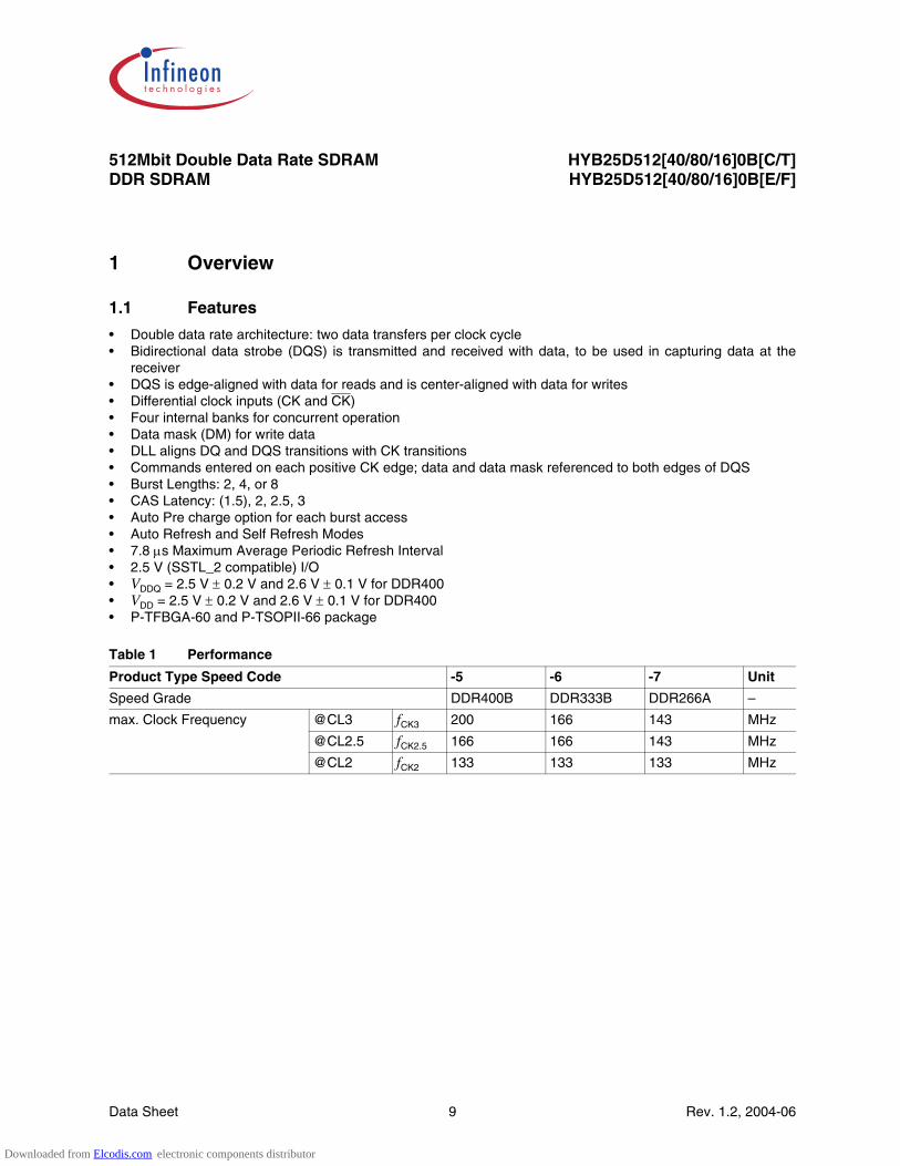
1.1 Features
• Double data rate architecture: two data transfers per clock cycle• Bidirectional data strobe (DQS) is transmitted and received with data, to be used in capturing data at the
receiver• DQS is edge-aligned with data for reads and is center-aligned with data for writes• Differential clock inputs (CK and CK)• Four internal banks for concurrent operation• Data mask (DM) for write data• DLL aligns DQ and DQS transitions with CK transitions• Commands entered on each positive CK edge; data and data mask referenced to both edges of DQS• Burst Lengths: 2, 4, or 8• CAS Latency: (1.5), 2, 2.5, 3• Auto Pre charge option for each burst access• Auto Refresh and Self Refresh Modes• 7.8 µs Maximum Average Periodic Refresh Interval• 2.5 V (SSTL_2 compatible) I/O• VDDQ = 2.5 V ± 0.2 V and 2.6 V ± 0.1 V for DDR400• VDD = 2.5 V ± 0.2 V and 2.6 V ± 0.1 V for DDR400• P-TFBGA-60 and P-TSOPII-66 package
Table 1 Performance
Product Type Speed Code -5 -6 -7 Unit
Speed Grade DDR400B DDR333B DDR266A –
max. Clock Frequency @CL3 fCK3 200 166 143 MHz
@CL2.5 fCK2.5 166 166 143 MHz
@CL2 fCK2 133 133 133 MHz
Downloaded from Elcodis.com electronic components distributor
HYB25D512[40/16/80]0B[E/F/C/T]512Mbit Double Data Rate SDRAM
Overview
Data Sheet 10 Rev. 1.2, 2004-06
1.2 Description
The 512Mbit Double Data Rate SDRAM is a high-speed CMOS, dynamic random-access memory containing536,870,912 bits. It is internally configured as a quad-bank DRAM.
The 512Mbit Double Data Rate SDRAM uses a double-data-rate architecture to achieve high-speed operation.The double data rate architecture is essentially a 2n pre fetch architecture with an interface designed to transfertwo data words per clock cycle at the I/O pins. A single read or write access for the 512Mbit Double Data RateSDRAM effectively consists of a single 2n-bit wide, one clock cycle data transfer at the internal DRAM core andtwo corresponding n-bit wide, one-half-clock-cycle data transfers at the I/O pins.
A bidirectional data strobe (DQS) is transmitted externally, along with data, for use in data capture at the receiver.DQS is a strobe transmitted by the DDR SDRAM during Reads and by the memory controller during Writes. DQSis edge-aligned with data for Reads and center-aligned with data for Writes.
The 512Mbit Double Data Rate SDRAM operates from a differential clock (CK and CK; the crossing of CK goingHIGH and CK going LOW is referred to as the positive edge of CK). Commands (address and control signals) areregistered at every positive edge of CK. Input data is registered on both edges of DQS, and output data isreferenced to both edges of DQS, as well as to both edges of CK.
Read and write accesses to the DDR SDRAM are burst oriented; accesses start at a selected location andcontinue for a programmed number of locations in a programmed sequence. Accesses begin with the registrationof an Active command, which is then followed by a Read or Write command. The address bits registeredcoincident with the Active command are used to select the bank and row to be accessed. The address bitsregistered coincident with the Read or Write command are used to select the bank and the starting column locationfor the burst access.
The DDR SDRAM provides for programmable Read or Write burst lengths of 2, 4 or 8 locations. An AutoPrecharge function may be enabled to provide a self-timed row precharge that is initiated at the end of the burstaccess.
As with standard SDRAMs, the pipelined, multibank architecture of DDR SDRAMs allows for concurrent operation,thereby providing high effective bandwidth by hiding row precharge and activation time.
An auto refresh mode is provided along with a power-saving power-down mode. All inputs are compatible with theJEDEC Standard for SSTL_2. All outputs are SSTL_2, Class II compatible.
Note: The functionality described and the timing specifications included in this data sheet are for the DLL Enabledmode of operation.
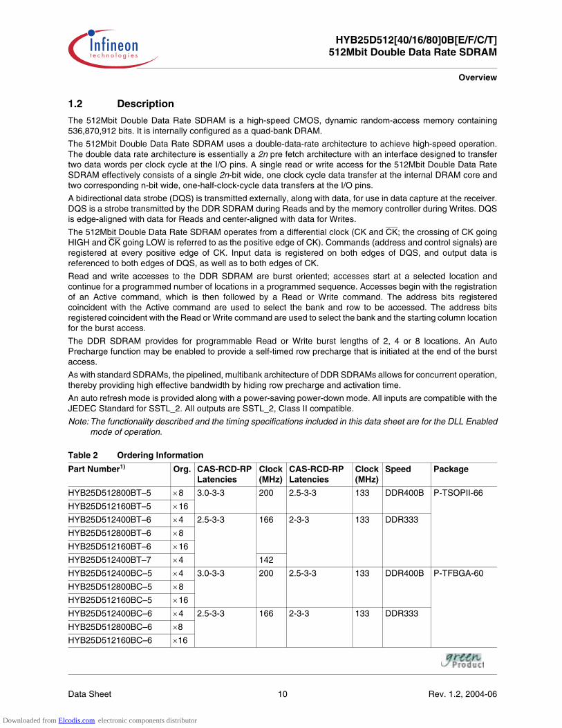
Table 2 Ordering Information
Part Number1) Org. CAS-RCD-RP Latencies
Clock (MHz)
CAS-RCD-RP Latencies
Clock (MHz)
Speed Package
HYB25D512800BT–5 ×8 3.0-3-3 200 2.5-3-3 133 DDR400B P-TSOPII-66
HYB25D512160BT–5 ×16
HYB25D512400BT–6 ×4 2.5-3-3 166 2-3-3 133 DDR333
HYB25D512800BT–6 ×8
HYB25D512160BT–6 ×16
HYB25D512400BT–7 ×4 142
HYB25D512400BC–5 ×4 3.0-3-3 200 2.5-3-3 133 DDR400B P-TFBGA-60
HYB25D512800BC–5 ×8
HYB25D512160BC–5 ×16
HYB25D512400BC–6 ×4 2.5-3-3 166 2-3-3 133 DDR333
HYB25D512800BC–6 ×8
HYB25D512160BC–6 ×16
Downloaded from Elcodis.com electronic components distributor

Data Sheet 11 Rev. 1.2, 2004-06
HYB25D512[40/16/80]0B[E/F/C/T]512Mbit Double Data Rate SDRAM
Overview
HYB25D512400BF–5 ×4 3.0-3-3 200 2.5-3-3 166 DDR400B P-TFBGA-60
HYB25D512160BF–5 ×16
HYB25D512400BF–6 ×4 2.5-3-3 166 2-3-3 133 DDR333
HYB25D512800BF–6 ×8
HYB25D512160BF–6 ×16
HYB25D512400BF–5 ×4 3.0-3-3 200 2.5-3-3 166 DDR400B P-TSOPII-66
HYB25D512800BE–5 ×8
HYB25D512160BE–5 ×16
HYB25D512400BE–6 ×4 2.5-3-3 166 2-3-3 133 DDR333
HYB25D512800BE–6 ×8
HYB25D512160BE–6 ×16
HYB25D512400BE–7 ×4 143 DDR266A
1) HYB: designator for memory components25D: DDR SDRAMs at VDDQ = 2.5 V512: 512-Mbit density400/800/160: Product variations x4, ×8 and ×16B: Die revision BC/F/E/T: Package type FBGA and TSOP
Table 2 Ordering Information (cont’d)
Part Number1) Org. CAS-RCD-RP Latencies
Clock (MHz)
CAS-RCD-RP Latencies
Clock (MHz)
Speed Package
Downloaded from Elcodis.com electronic components distributor

HYB25D512[40/16/80]0B[E/F/C/T]512Mbit Double Data Rate SDRAM
Pin Configuration
Data Sheet 12 Rev. 1.2, 2004-06
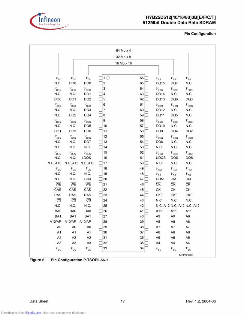
2 Pin ConfigurationThe pin configuration of a DDR SDRAM is listed by function in Table 3 (60 pins). The abbreviations used in thePin#/Buffer# column are explained in Table 4 and Table 5 respectively. The pin numbering for FBGA is depictedin Figure 1 and that of the TSOP package in Figure 2
Table 3 Pin Configuration of DDR SDRAM
Ball#/Pin# Name PinType
BufferType
Function
Clock Signals
G2, 45 CK I SSTL Clock Signal
G3, 46 CK I SSTL Complementary Clock Signal
H3, 44 CKE I SSTL Clock Enable Rank
Control Signals
H7, 23 RAS I SSTL Row Address Strobe
G8, 22 CAS I SSTL Column Address Strobe
G7, 21 WE I SSTL Write Enable
H8, 24 CS I SSTL Chip Select
Address Signals
J8, 26 BA0 I SSTL Bank Address Bus 2:0
J7, 27 BA1 I SSTL
K7, 29 A0 I SSTL Address Bus 11:0
L8, 30 A1 I SSTL
L7, 31 A2 I SSTL
M8, 32 A3 I SSTL
M2, 35 A4 I SSTL
L3, 36 A5 I SSTL
L2, 37 A6 I SSTL
K3, 38 A7 I SSTL
K2, 39 A8 I SSTL
J3, 40 A9 I SSTL
K8, 28 A10 I SSTL
AP I SSTL
J2, 41 A11 I SSTL
H2, 42 A12 I SSTL Address Signal 12
Note: 256 Mbit or larger dies
NC NC — Note: 128 Mbit or smaller dies
F9, 17 A13 I SSTL Address Signal 13
Note: 1 Gbit based dies
NC NC — Note: 512 Mbit or smaller dies
Downloaded from Elcodis.com electronic components distributor

Data Sheet 13 Rev. 1.2, 2004-06
HYB25D512[40/16/80]0B[E/F/C/T]512Mbit Double Data Rate SDRAM
Pin Configuration
Data Signals ×4 organization
B7, 5 DQ0 I/O SSTL Data Signal 3:0
D7, 11 DQ1 I/O SSTL
D3, 56 DQ2 I/O SSTL
B3, 62 DQ3 I/O SSTL
Data Strobe ×4 organisation
E3, 51 DQS I/O SSTL Data Strobe
Data Mask ×4 organization
F3, 47 DM I SSTL Data Mask
Data Signals ×8 organization
A8, 2 DQ0 I/O SSTL Data Signal 7:0
B7, 5 DQ1 I/O SSTL
C7, 8 DQ2 I/O SSTL
D7, 11 DQ3 I/O SSTL
D3, 56 DQ4 I/O SSTL
C3, 59 DQ5 I/O SSTL
B3, 62 DQ6 I/O SSTL
A2, 65 DQ7 I/O SSTL
Data Strobe ×8 organisation
E3, 51 DQS I/O SSTL Data Strobe
Data Mask ×8 organization
F3, 47 DM I SSTL Data Mask
Data Signals ×16 organization
A8, 2 DQ0 I/O SSTL Data Signal 15:0
B9, 4 DQ1 I/O SSTL
B7, 5 DQ2 I/O SSTL
C9, 7 DQ3 I/O SSTL
C7, 8 DQ4 I/O SSTL
D9, 10 DQ5 I/O SSTL
D7, 11 DQ6 I/O SSTL
E9, 13 DQ7 I/O SSTL
E1, 54 DQ8 I/O SSTL
D3, 56 DQ9 I/O SSTL
D1, 57 DQ10 I/O SSTL
C3, 59 DQ11 I/O SSTL
C1, 60 DQ12 I/O SSTL
B3, 62 DQ13 I/O SSTL
B1, 63 DQ14 I/O SSTL
A2, 65 DQ15 I/O SSTL
Table 3 Pin Configuration of DDR SDRAM
Ball#/Pin# Name PinType
BufferType
Function
Downloaded from Elcodis.com electronic components distributor
HYB25D512[40/16/80]0B[E/F/C/T]512Mbit Double Data Rate SDRAM
Pin Configuration
Data Sheet 14 Rev. 1.2, 2004-06
Data Strobe ×16 organization
E3, 51 UDQS I/O SSTL Data Strobe Upper Byte
E7, 16 LDQS I/O SSTL Data Strobe Lower Byte
Data Mask ×16 organization
F3, 47 UDM I SSTL Data Mask Upper Byte
F7, 20 LDM I SSTL Data Mask Lower Byte
Power Supplies
F1, 49 VREF AI — I/O Reference Voltage
A9, B2, C8, D2, E8, 3, 9, 15, 55, 61
VDDQ PWR — I/O Driver Power Supply
A7, F8, M3, M7, 1, 18, 33
VDD PWR — Power Supply
A1, B8, C2, D8, E2, 6, 12, 52, 58, 64
VSSQ PWR — Power Supply
F2, 34 VSS PWR — Power Supply
Not Connected
A2, 65 NC NC — Not Connected
Note: ×4 organization
A8, 2 NC NC — Not Connected
Note: ×4 organization
B1, 63 NC NC — Not Connected
Note: ×8 and ×4 organisation
B9, 4 NC NC — Not Connected
Note: ×8 and ×4 organization
C1, 60 NC NC — Not Connected
Note: ×8 and ×4 organization
C3, 59 NC NC — Not Connected
Note: ×4 organization
C7, 8 NC NC — Not Connected
Note: ×4 organization
C9, 7 NC NC — Not Connected
Note: ×8 and ×4 organization
D1, 57 NC NC — Not Connected
Note: ×8 and ×4 organization
D9, 10 NC NC — Not Connected
Note: ×8 and ×4 organization
E1, 54 NC NC — Not Connected
Note: ×8 and ×4 organization
Table 3 Pin Configuration of DDR SDRAM
Ball#/Pin# Name PinType
BufferType
Function
Downloaded from Elcodis.com electronic components distributor

Data Sheet 15 Rev. 1.2, 2004-06
HYB25D512[40/16/80]0B[E/F/C/T]512Mbit Double Data Rate SDRAM
Pin Configuration
E7, 16 NC NC — Not Connected
Note: ×8 and ×4 organization
E9, 13 NC NC — Not Connected
Note: ×8 and ×4 organization
F7, 20 NC NC — Not Connected
Note: ×8 and ×4 organization
F9, 14, 17, 19, 25,43, 50, 53
NC NC — Not Connected
Note: ×16,×8 and ×4 organization
Table 4 Abbreviations for Pin Type
Abbreviation Description
I Standard input-only pin. Digital levels.
O Output. Digital levels.
I/O I/O is a bidirectional input/output signal.
AI Input. Analog levels.
PWR Power
GND Ground
NC Not Connected
Table 5 Abbreviations for Buffer Type
Abbreviation Description
SSTL Serial Stub Terminated Logic (SSTL2)
LV-CMOS Low Voltage CMOS
CMOS CMOS Levels
OD Open Drain. The corresponding pin has 2 operational states, active low and tristate, and allows multiple devices to share as a wire-OR.
Table 3 Pin Configuration of DDR SDRAM
Ball#/Pin# Name PinType
BufferType
Function
Downloaded from Elcodis.com electronic components distributor

HYB25D512[40/16/80]0B[E/F/C/T]512Mbit Double Data Rate SDRAM
Pin Configuration
Data Sheet 16 Rev. 1.2, 2004-06
Figure 1 Pin Configuration P-TFBGA-60-9 Top View, see the balls throught the package
,
,
,
Downloaded from Elcodis.com electronic components distributor
Data Sheet 17 Rev. 1.2, 2004-06
HYB25D512[40/16/80]0B[E/F/C/T]512Mbit Double Data Rate SDRAM
Pin Configuration
Figure 2 Pin Configuration P-TSOPII-66-1
!"!#!
!"!#!
!"!#!
Downloaded from Elcodis.com electronic components distributor

HYB25D512[40/16/80]0B[E/F/C/T]512Mbit Double Data Rate SDRAM
Pin Configuration
Data Sheet 18 Rev. 1.2, 2004-06
Table 6 Input/Output Functional Description
Symbol Type Function
CK, CK Input Clock: CK and CK are differential clock inputs. All address and control input signals are sampled on the crossing of the positive edge of CK and negative edge of CK. Output (read) data is referenced to the crossings of CK and CK (both directions of crossing).
CKE Input Clock Enable: CKE HIGH activates, and CKE Low deactivates, internal clock signals and device input buffers and output drivers. Taking CKE Low provides Precharge Power-Down and Self Refresh operation (all banks idle), or Active Power-Down (row Active in any bank). CKE is synchronous for power down entry and exit, and for self refresh entry. CKE is asynchronous for self refresh exit. CKE must be maintained high throughout read and write accesses. Input buffers, excluding CK, CK and CKE are disabled during power-down. Input buffers, excluding CKE, are disabled during self refresh. CKE is an SSTL_2 input, but will detect an LVCMOS LOW level after VDD is applied on first power up. After VREF has become stable during the power on and initialization sequence, it must be mantained for proper operation of the CKE receiver. For proper self-refresh entry and exit, VREF must be mantained to this input.
CS Input Chip Select: All commands are masked when CS is registered HIGH. CS provides for external bank selection on systems with multiple banks. CS is considered part of the command code. The standard pinout includes one CS pin.
RAS, CAS, WE Input Command Inputs: RAS, CAS and WE (along with CS) define the command being entered.
DM Input Input Data Mask: DM is an input mask signal for write data. Input data is masked when DM is sampled HIGH coincident with that input data during a Write access. DM is sampled on both edges of DQS. Although DM pins are input only, the DM loading matches the DQ and DQS loading.
BA0, BA1 Input Bank Address Inputs: BA0 and BA1 define to which bank an Active, Read, Write or Precharge command is being applied. BA0 and BA1 also determines if the mode register or extended mode register is to be accessed during a MRS or EMRS cycle.
A0 - A12 Input Address Inputs: Provide the row address for Active commands, and the column address and Auto Precharge bit for Read/Write commands, to select one location out of the memory array in the respective bank. A10 is sampled during a Precharge command to determine whether the Precharge applies to one bank (A10 LOW) or all banks (A10 HIGH). If only one bank is to be precharged, the bank is selected by BA0, BA1. The address inputs also provide the op-code during a Mode Register Set command.
DQ Input/Output Data Input/Output: Data bus.
DQS Input/Output Data Strobe: Output with read data, input with write data. Edge-aligned with read data, centered in write data. Used to capture write data.
N.C. – No Connect: No internal electrical connection is present.
VDDQ Supply DQ Power Supply: 2.5 V ± 0.2 V and 2.6 V ± 0.1 V for DDR400
VSSQ Supply DQ Ground
VDD Supply Power Supply: 2.5 V ± 0.2 V and 2.6 V ± 0.1 V for DDR400
VSS Supply Ground
VREF Supply SSTL_2 Reference Voltage: (VDDQ/2)
Downloaded from Elcodis.com electronic components distributor
Data Sheet 19 Rev. 1.2, 2004-06
HYB25D512[40/16/80]0B[E/F/C/T]512Mbit Double Data Rate SDRAM
Pin Configuration
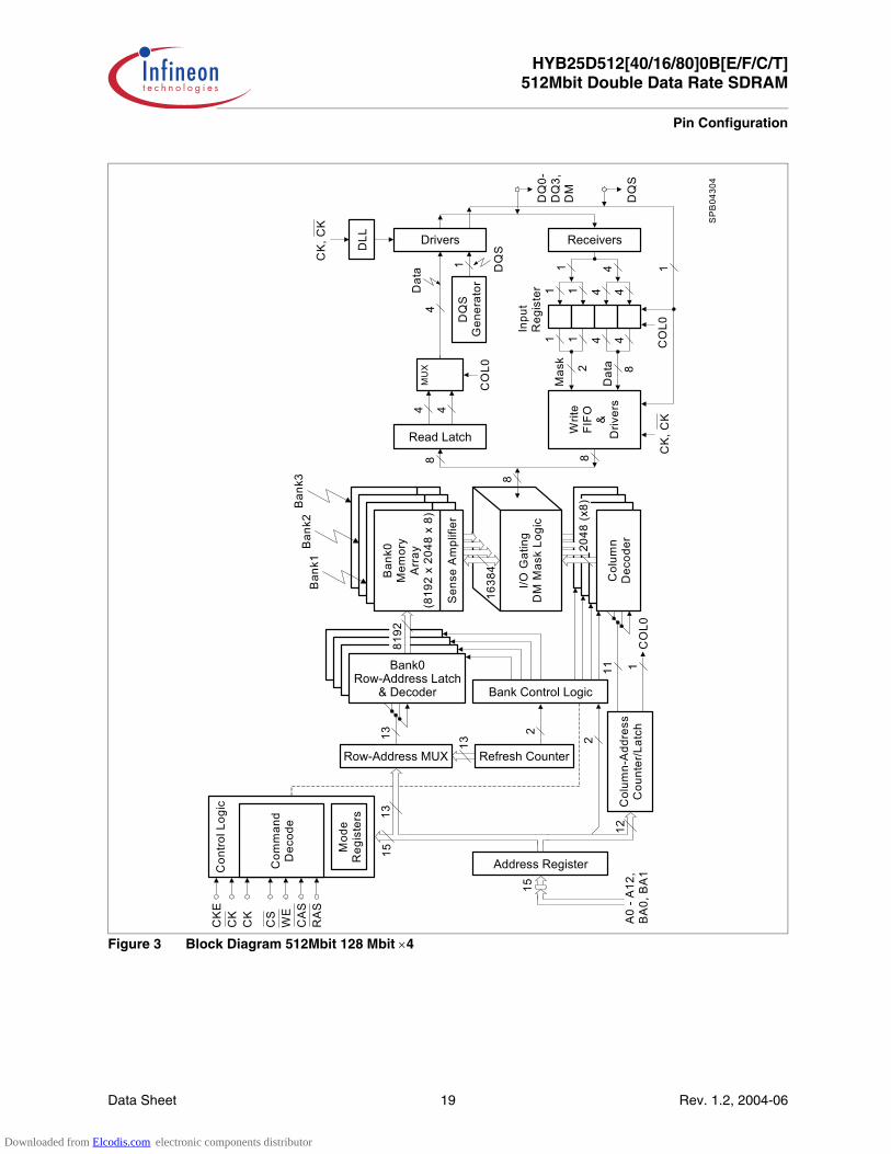
Figure 3 Block Diagram 512Mbit 128 Mbit ×4
SP
B04
304
Con
trol L
ogic
Row-Address MUX
8192
Bank0Row-Address Latch
& Decoder Bank Control Logic
Col
umn
Dec
oder
Col
umn
Dec
oder
Col
umn
Dec
oder
I/O G
atin
gD
M M
ask
Logi
c
1638
4
Sen
se A
mpl
ifier
Ban
k0M
emor
yA
rray
(819
2 x
2048
x 8
)
Ban
k1
2048
(x8)
Refresh Counter
13 2
Col
umn
Dec
oder
2
Col
umn-
Add
ress
Cou
nter
/Lat
ch
11 1C
OL0
Address Register
12
1315M
ode
Reg
iste
rs
Com
man
dD
ecod
e
RA
SC
AS
WE
CS
CK
CK
CK
E
A0
- A12
,B
A0,
BA
1
8
1 1 4 4
1 4
1 1 4 4
2 8
Dat
a
Mas
kW
rite
FIFO &
Driv
ers
8
CO
L0C
K, C
K
Receivers
Inpu
tR
egis
ter
MU
X
CO
L0
DQ
SG
ener
ator
Drivers
4
1
Dat
a DQ
S
4 4Read Latch
8
1
DLL
CK
, CK
DQ
S
DQ
0-D
Q3,
DM
15
13
Ban
k2B
ank3
Downloaded from Elcodis.com electronic components distributor
HYB25D512[40/16/80]0B[E/F/C/T]512Mbit Double Data Rate SDRAM
Pin Configuration
Data Sheet 20 Rev. 1.2, 2004-06
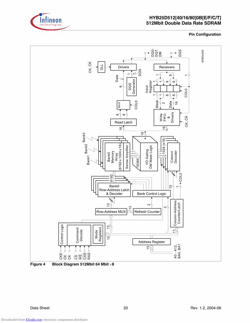
Figure 4 Block Diagram 512Mbit 64 Mbit ×8
SP
B04
305
Con
trol L
ogic
Row-Address MUX
8192
Bank0Row-Address Latch
& Decoder Bank Control Logic
Col
umn
Dec
oder
Col
umn
Dec
oder
Col
umn
Dec
oder
I/O G
atin
gD
M M
ask
Logi
c
1638
4
Sen
se A
mpl
ifier
Ban
k0M
emor
yA
rray
(819
2 x
1024
x 1
6)
Ban
k1
1024
(x16
)
Refresh Counter
13 2
Col
umn
Dec
oder
2
Col
umn-
Add
ress
Cou
nter
/Lat
ch
10 1C
OL0
Address Register
11
1315M
ode
Reg
iste
rs
Com
man
dD
ecod
e
RA
SC
AS
WE
CS
CK
CK
CK
E
A0
- A12
,B
A0,
BA
1
16
1 1 8 8
1 8
1 1 8 8
2 16
Dat
a
Mas
kW
rite
FIFO &
Driv
ers
16
CO
L0C
K, C
K
Receivers
Inpu
tR
egis
ter
MU
X
CO
L0
DQ
SG
ener
ator
Drivers
8
1
Dat
a DQ
S
8 8Read Latch
16
1
DLL
CK
, CK
DQ
S
DQ
0-D
Q7,
DM
15
13
Ban
k2B
ank3
Downloaded from Elcodis.com electronic components distributor
Data Sheet 21 Rev. 1.2, 2004-06
HYB25D512[40/16/80]0B[E/F/C/T]512Mbit Double Data Rate SDRAM
Pin Configuration
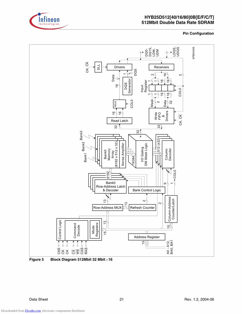
Figure 5 Block Diagram 512Mbit 32 Mbit ×16
SP
B04
306
Con
trol L
ogic
Row-Address MUX
8192
Bank0Row-Address Latch
& Decoder Bank Control Logic
Col
umn
Dec
oder
Col
umn
Dec
oder
Col
umn
Dec
oder
I/O G
atin
gD
M M
ask
Logi
c
1638
4
Sen
se A
mpl
ifier
Ban
k0M
emor
yA
rray
(819
2 x
512
x 32
)
Ban
k1
512
(x32
)
Refresh Counter
13 2
Col
umn
Dec
oder
2
Col
umn-
Add
ress
Cou
nter
/Lat
ch
9 1C
OL0
Address Register
10
1315M
ode
Reg
iste
rs
Com
man
dD
ecod
e
RA
SC
AS
WE
CS
CK
CK
CK
E
A0
- A12
,B
A0,
BA
1
32
1 1 16 16
2 16
1 1 16 16
2 32
Dat
a
Mas
kW
rite
FIFO &
Driv
ers
32
CO
L0C
K, C
K
Receivers
Inpu
tR
egis
ter
MU
X
CO
L0
DQ
SG
ener
ator
Drivers
16
1
Dat
a DQ
S
16 16Read Latch
32
2
DLL
CK
, CK
LDQ
S,
UD
QS
DQ
0-D
Q15
,LD
M,
UD
M
15
13
Ban
k2B
ank3
Downloaded from Elcodis.com electronic components distributor

HYB25D512[40/16/80]0B[E/F/C/T]512Mbit Double Data Rate SDRAM
Functional Description
Data Sheet 22 Rev. 1.2, 2004-06
3 Functional DescriptionThe 512Mbit Double Data Rate SDRAM is a high-speed CMOS, dynamic random-access memory containing536,870,912 bits. The 512Mbit Double Data Rate SDRAM is internally configured as a quad-bank DRAM.
The 512Mbit Double Data Rate SDRAM uses a double-data-rate architecture to achieve high-speed operation.The double-data-rate architecture is essentially a 2n pre fetch architecture, with an interface designed to transfertwo data words per clock cycle at the I/O pins. A single read or write access for the 512Mbit Double Data RateSDRAM consists of a single 2n-bit wide, one clock cycle data transfer at the internal DRAM core and twocorresponding n-bit wide, one-half clock cycle data transfers at the I/O pins.
Read and write accesses to the DDR SDRAM are burst oriented; accesses start at a selected location andcontinue for a programmed number of locations in a programmed sequence. Accesses begin with the registrationof an Active command, which is then followed by a Read or Write command. The address bits registeredcoincident with the Active command are used to select the bank and row to be accessed (BA0, BA1 select thebank; A0-A12 select the row). The address bits registered coincident with the Read or Write command are usedto select the starting column location for the burst access.
Prior to normal operation, the DDR SDRAM must be initialized. The following sections provide detailed informationcovering device initialization, register definition, command descriptions and device operation.
3.1 Initialization
DDR SDRAMs must be powered up and initialized in a predefined manner. Operational procedures other thanthose specified may result in undefined operation. The following criteria must be met:
No power sequencing is specified during power up or power down given the following criteria:
• VDD and VDDQ are driven from a single power converter output• VTT meets the specification• A minimum resistance of 42 Ω limits the input current from the VTT supply into any pin and VREF tracks VDDQ/2
or the following relationship must be followed:
• VDDQ is driven after or with VDD such that VDDQ < VDD + 0.3 V• VTT is driven after or with VDDQ such that VTT < VDDQ + 0.3 V• VREF is driven after or with VDDQ such that VREF < VDDQ + 0.3 V
The DQ and DQS outputs are in the High-Z state, where they remain until driven in normal operation (by a readaccess). After all power supply and reference voltages are stable, and the clock is stable, the DDR SDRAMrequires a 200 µs delay prior to applying an executable command.
Once the 200 µs delay has been satisfied, a Deselect or NOP command should be applied, and CKE should bebrought HIGH. Following the NOP command, a Precharge ALL command should be applied. Next a ModeRegister Set command should be issued for the Extended Mode Register, to enable the DLL, then a ModeRegister Set command should be issued for the Mode Register, to reset the DLL, and to program the operatingparameters. 200 clock cycles are required between the DLL reset and any executable command. During the200 cycles of clock for DLL locking, a Deselect or NOP command must be applied. After the 200 clock cycles, aPrecharge ALL command should be applied, placing the device in the “all banks idle” state.
Once in the idle state, two AUTO REFRESH cycles must be performed. Additionally, a Mode Register Setcommand for the Mode Register, with the reset DLL bit deactivated (i.e. to program operating parameters withoutresetting the DLL) must be performed. Following these cycles, the DDR SDRAM is ready for normal operation.
Downloaded from Elcodis.com electronic components distributor

Data Sheet 23 Rev. 1.2, 2004-06
HYB25D512[40/16/80]0B[E/F/C/T]512Mbit Double Data Rate SDRAM
Functional Description
3.2 Mode Register Definition
The Mode Register is used to define the specific mode of operation of the DDR SDRAM. This definition includesthe selection of a burst length, a burst type, a CAS latency, and an operating mode. The Mode Register isprogrammed via the Mode Register Set command (with BA0 = 0 and BA1 = 0) and retains the stored informationuntil it is programmed again or the device loses power (except for bit A8, which is self-clearing).
Mode Register bits A0-A2 specify the burst length, A3 specifies the type of burst (sequential or interleaved), A4-A6 specify the CAS latency, and A7-A12 specify the operating mode.
The Mode Register must be loaded when all banks are idle, and the controller must wait the specified time beforeinitiating the subsequent operation. Violating either of these requirements results in unspecified operation.
3.2.1 Burst LengthRead and write accesses to the DDR SDRAM are burst oriented, with the burst length being programmable. Theburst length determines the maximum number of column locations that can be accessed for a given Read or Writecommand. Burst lengths of 2, 4, or 8 locations are available for both the sequential and the interleaved burst types.
Reserved states should not be used, as unknown operation or incompatibility with future versions may result.
When a Read or Write command is issued, a block of columns equal to the burst length is effectively selected. Allaccesses for that burst take place within this block, meaning that the burst wraps within the block if a boundary is
MRMode Register Definition (BA[1:0] = 00B)
BA1 BA0 A12 A11 A10 A9 A8 A7 A6 A5 A4 A3 A2 A1 A0
0 0 MODE CL BT BL
reg. addr w w w w
Field Bits Type Description
BL [2:0] w Burst LengthNumber of sequential bits per DQ related to one read/write command; see Chapter 3.2.1.
Note: All other bit combinations are RESERVED.
001 2010 4011 8
BT 3 w Burst TypeSee Table 7 for internal address sequence of low order address bits; see Chapter 3.2.2.0 Sequential1 Interleaved
CL [6:4] w CAS LatencyNumber of full clocks from read command to first data valid window; see Chapter 3.2.3.
Note: All other bit combinations are RESERVED.
010 2011 3101 (1.5 Optional, not covered by this data sheet)110 2.5
MODE [12:7] w Operating ModeSee Chapter 3.2.4.
Note: All other bit combinations are RESERVED.
000000 Normal Operation without DLL Reset000010 DLL Reset
Downloaded from Elcodis.com electronic components distributor

HYB25D512[40/16/80]0B[E/F/C/T]512Mbit Double Data Rate SDRAM
Functional Description
Data Sheet 24 Rev. 1.2, 2004-06
reached. The block is uniquely selected by A1-Ai when the burst length is set to two, by A2-Ai when the burstlength is set to four and by A3-Ai when the burst length is set to eight (where Ai is the most significant columnaddress bit for a given configuration). The remaining (least significant) address bit(s) is (are) used to select thestarting location within the block. The programmed burst length applies to both Read and Write bursts.
3.2.2 Burst TypeAccesses within a given burst may be programmed to be either sequential or interleaved; this is referred to as theburst type and is selected via bit A3. The ordering of accesses within a burst is determined by the burst length, theburst type and the starting column address, as shown in Table 7.
Notes
1. For a burst length of two, A1-Ai selects the two-data-element block; A0 selects the first access within the block.2. For a burst length of four, A2-Ai selects the four-data-element block; A0-A1 selects the first access within the
block.3. For a burst length of eight, A3-Ai selects the eight-data- element block; A0-A2 selects the first access within
the block.4. Whenever a boundary of the block is reached within a given sequence above, the following access wraps
within the block.
3.2.3 Read LatencyThe Read latency, or CAS latency, is the delay, in clock cycles, between the registration of a Read command andthe availability of the first burst of output data. The latency can be programmed 2, 2.5 and 3 clocks. CAS latencyof 1.5 is an optional feature on this device.
If a Read command is registered at clock edge n, and the latency is m clocks, the data is available nominallycoincident with clock edge n + m.
Reserved states should not be used as unknown operation or incompatibility with future versions may result.
Table 7 Burst Definition
Burst Length
Starting Column Address Order of Accesses Within a Burst
A2 A1 A0 Type = Sequential Type = Interleaved
2 0 0-1 0-1
1 1-0 1-0
4 0 0 0-1-2-3 0-1-2-3
0 1 1-2-3-0 1-0-3-2
1 0 2-3-0-1 2-3-0-1
1 1 3-0-1-2 3-2-1-0
8 0 0 0 0-1-2-3-4-5-6-7 0-1-2-3-4-5-6-7
0 0 1 1-2-3-4-5-6-7-0 1-0-3-2-5-4-7-6
0 1 0 2-3-4-5-6-7-0-1 2-3-0-1-6-7-4-5
0 1 1 3-4-5-6-7-0-1-2 3-2-1-0-7-6-5-4
1 0 0 4-5-6-7-0-1-2-3 4-5-6-7-0-1-2-3
1 0 1 5-6-7-0-1-2-3-4 5-4-7-6-1-0-3-2
1 1 0 6-7-0-1-2-3-4-5 6-7-4-5-2-3-0-1
1 1 1 7-0-1-2-3-4-5-6 7-6-5-4-3-2-1-0
Downloaded from Elcodis.com electronic components distributor
Data Sheet 25 Rev. 1.2, 2004-06
HYB25D512[40/16/80]0B[E/F/C/T]512Mbit Double Data Rate SDRAM
Functional Description
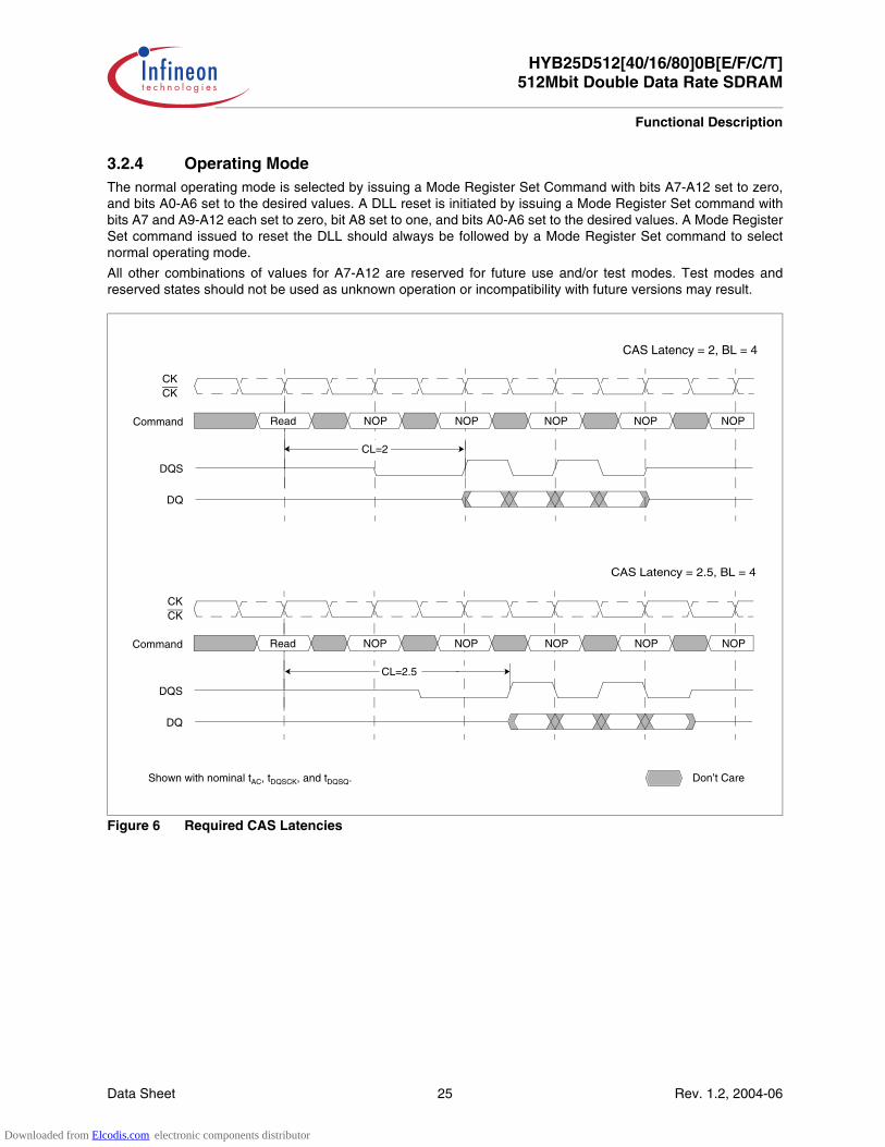
3.2.4 Operating ModeThe normal operating mode is selected by issuing a Mode Register Set Command with bits A7-A12 set to zero,and bits A0-A6 set to the desired values. A DLL reset is initiated by issuing a Mode Register Set command withbits A7 and A9-A12 each set to zero, bit A8 set to one, and bits A0-A6 set to the desired values. A Mode RegisterSet command issued to reset the DLL should always be followed by a Mode Register Set command to selectnormal operating mode.
All other combinations of values for A7-A12 are reserved for future use and/or test modes. Test modes andreserved states should not be used as unknown operation or incompatibility with future versions may result.
Figure 6 Required CAS Latencies
NOP NOP NOP NOP NOPRead
CAS Latency = 2, BL = 4
Shown with nominal tAC, tDQSCK, and tDQSQ.
CKCK
Command
DQS
DQ
Don’t Care
CL=2
NOP NOP NOP NOP NOPRead
CAS Latency = 2.5, BL = 4
CKCK
Command
DQS
DQ
CL=2.5
Downloaded from Elcodis.com electronic components distributor

HYB25D512[40/16/80]0B[E/F/C/T]512Mbit Double Data Rate SDRAM
Functional Description
Data Sheet 26 Rev. 1.2, 2004-06
3.3 Extended Mode Register
The Extended Mode Register controls functions beyond those controlled by the Mode Register; these additionalfunctions include DLL enable/disable, and output drive strength selection (optional). These functions are controlledvia the bits shown in the Extended Mode Register Definition. The Extended Mode Register is programmed via theMode Register Set command (with BA0 = 1 and BA1 = 0) and retains the stored information until it is programmedagain or the device loses power. The Extended Mode Register must be loaded when all banks are idle, and thecontroller must wait the specified time before initiating any subsequent operation. Violating either of theserequirements result in unspecified operation.
3.3.1 DLL Enable/DisableThe DLL must be enabled for normal operation. DLL enable is required during power up initialization, and uponreturning to normal operation after having disabled the DLL for the purpose of debug or evaluation. The DLL isautomatically disabled when entering self refresh operation and is automatically re-enabled upon exit of selfrefresh operation. Any time the DLL is enabled, 200 clock cycles must occur before a Read command can beissued. This is the reason 200 clock cycles must occur before issuing a Read or Write command upon exit of selfrefresh operation.
3.3.2 Output Drive StrengthThe normal drive strength for all outputs is specified to be SSTL_2, Class II. In addition this design versionsupports a weak driver mode for lighter load and/or point-to-point environments which can be activated duringmode register set. I-V curves for the normal and weak drive strength are included in this document.
EMRExtended Mode Register Definition (BA[1:0] = 01B)
BA1 BA0 A12 A11 A10 A9 A8 A7 A6 A5 A4 A3 A2 A1 A0
0 1 MODE DS DLL
reg. addr w w w
Field Bits Type Description
DLL 0 w DLL StatusSee Chapter 3.3.1.0 Enabled1 Disabled
DS 1 w Drive StrengthSee Chapter 3.3.2, Chapter 5 and Chapter 5.1.0 Normal1 Weak
MODE [12:2] w Operating Mode
Note: All other bit combinations are RESERVED.
0 Normal Operation
Downloaded from Elcodis.com electronic components distributor
Data Sheet 27 Rev. 1.2, 2004-06
HYB25D512[40/16/80]0B[E/F/C/T]512Mbit Double Data Rate SDRAM
Functional Description
3.4 Commands
Deselect
The Deselect function prevents new commands from being executed by the DDR SDRAM. The DDR SDRAM iseffectively deselected. Operations already in progress are not affected.
No Operation (NOP)
The No Operation (NOP) command is used to perform a NOP to a DDR SDRAM. This prevents unwantedcommands from being registered during idle or wait states. Operations already in progress are not affected.
Mode Register Set
The mode registers are loaded via inputs A0-A12, BA0 and BA1. See mode register descriptions in Chapter 3.2.The Mode Register Set command can only be issued when all banks are idle and no bursts are in progress. Asubsequent executable command cannot be issued until tMRD is met.
Active
The Active command is used to open (or activate) a row in a particular bank for a subsequent access. The valueon the BA0, BA1 inputs selects the bank, and the address provided on inputs A0-A12 selects the row. This rowremains active (or open) for accesses until a Precharge (or Read or Write with Auto Precharge) is issued to thatbank. A Precharge (or Read or Write with Auto Precharge) command must be issued and completed beforeopening a different row in the same bank.
Read
The Read command is used to initiate a burst read access to an active (open) row. The value on the BA0, BA1inputs selects the bank, and the address provided on inputs A0-Ai, Aj (where [i = 8, j = don’t care] for x16, [i = 9,j = don’t care] for x8 and [i = 9, j = 11] for x4) selects the starting column location. The value on input A10determines whether or not Auto Precharge is used. If Auto Precharge is selected, the row being accessed isprecharged at the end of the Read burst; if Auto Precharge is not selected, the row remains open for subsequentaccesses.
Write
The Write command is used to initiate a burst write access to an active (open) row. The value on the BA0, BA1inputs selects the bank, and the address provided on inputs A0-Ai, Aj (where [i = 9, j = don’t care] for x8; where[i = 9, j = 11] for x4) selects the starting column location. The value on input A10 determines whether or not AutoPrecharge is used. If Auto Precharge is selected, the row being accessed is precharged at the end of the Writeburst; if Auto Precharge is not selected, the row remains open for subsequent accesses. Input data appearing onthe DQs is written to the memory array subject to the DM input logic level appearing coincident with the data. If agiven DM signal is registered low, the corresponding data is written to memory; if the DM signal is registered high,the corresponding data inputs are ignored, and a Write is not executed to that byte/column location.
Pre charge
The Pre charge command is used to deactivate (close) the open row in a particular bank or the open row(s) in allbanks. The bank(s) will be available for a subsequent row access a specified time (tRP) after the Prechargecommand is issued. Input A10 determines whether one or all banks are to be pre charged, and in the case whereonly one bank is to be pre charged, inputs BA0, BA1 select the bank. Otherwise BA0, BA1 are treated as “Don’tCare”. Once a bank has been pre charged, it is in the idle state and must be activated prior to any Read or Writecommands being issued to that bank. A precharge command is treated as a NOP if there is no open row in thatbank, or if the previously open row is already in the process of pre charging.
Downloaded from Elcodis.com electronic components distributor

HYB25D512[40/16/80]0B[E/F/C/T]512Mbit Double Data Rate SDRAM
Functional Description
Data Sheet 28 Rev. 1.2, 2004-06
Auto Pre charge
Auto Pre charge is a feature which performs the same individual-bank precharge functions described above, butwithout requiring an explicit command. This is accomplished by using A10 to enable Auto Precharge in conjunctionwith a specific Read or Write command. A precharge of the bank/row that is addressed with the Read or Writecommand is automatically performed upon completion of the Read or Write burst. Auto Pre charge is nonpersistent in that it is either enabled or disabled for each individual Read or Write command. Auto Pre chargeensures that the pre charge is initiated at the earliest valid stage within a burst. The user must not issue anothercommand to the same bank until the precharge (tRP) is completed. This is determined as if an explicit Pre chargecommand was issued at the earliest possible time, as described for each burst type in Chapter 3.5.
Burst Terminate
The Burst Terminate command is used to truncate read bursts (with Auto Pre charge disabled). The most recentlyregistered Read command prior to the Burst Terminate command is truncated, as shown in Chapter 3.5.
Auto Refresh
Auto Refresh is used during normal operation of the DDR SDRAM and is analogous to CAS Before RAS (CBR)Refresh in previous DRAM types. This command is non persistent, so it must be issued each time a refresh isrequired.
The refresh addressing is generated by the internal refresh controller. This makes the address bits “Don’t Care”during an Auto Refresh command. The 512Mbit Double Data Rate SDRAM requires Auto Refresh cycles at anaverage periodic interval of 7.8 µs (maximum).
To allow for improved efficiency in scheduling and switching between tasks, some flexibility in the absolute refreshinterval is provided. A maximum of eight Auto Refresh commands can be posted in the system, meaning that themaximum absolute interval between any Auto Refresh command and the next Auto Refresh command is9 × 7.8 µs (70.2 µs). This maximum absolute interval is short enough to allow for DLL updates internal to the DDRSDRAM to be restricted to Auto Refresh cycles, without allowing too much drift in tAC between updates.
Self Refresh
The Self Refresh command can be used to retain data in the DDR SDRAM, even if the rest of the system ispowered down. When in the self refresh mode, the DDR SDRAM retains data without external clocking. The SelfRefresh command is initiated as an Auto Refresh command coincident with CKE transitioning low. The DLL isautomatically disabled upon entering Self Refresh, and is automatically enabled upon exiting Self Refresh(200 clock cycles must then occur before a Read command can be issued). Input signals except CKE (low) are“Don’t Care” during Self Refresh operation. Since CKE is an SSTL_2 input , VREF must be maintained during SELFREFRESH. The procedure for exiting self refresh requires a sequence of commands. CK (and CK) must be stable prior to CKEreturning high. Once CKE is high, the SDRAM must have NOP commands issued for tXSNR because time isrequired for the completion of any internal refresh in progress. A simple algorithm for meeting both refresh andDLL requirements is to apply NOPs for 200 clock cycles before applying any other command.
Downloaded from Elcodis.com electronic components distributor
Data Sheet 29 Rev. 1.2, 2004-06
HYB25D512[40/16/80]0B[E/F/C/T]512Mbit Double Data Rate SDRAM
Functional Description
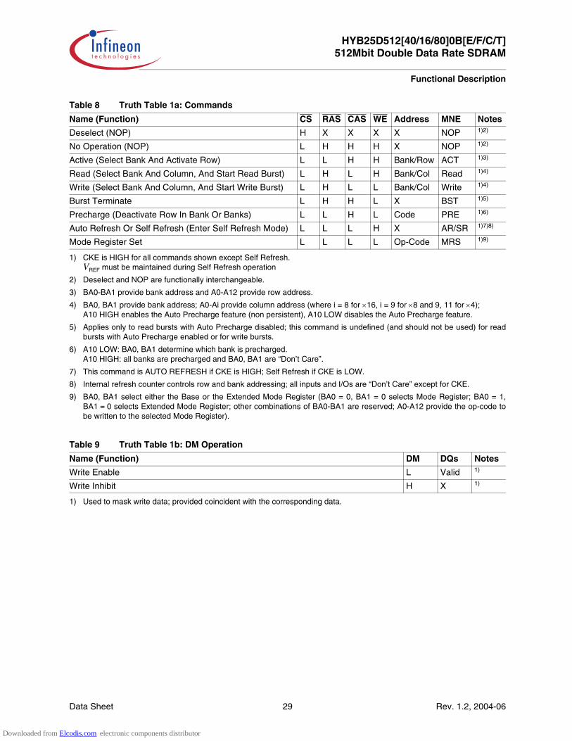
Table 8 Truth Table 1a: Commands
Name (Function) CS RAS CAS WE Address MNE Notes
Deselect (NOP) H X X X X NOP 1)2)
No Operation (NOP) L H H H X NOP 1)2)
Active (Select Bank And Activate Row) L L H H Bank/Row ACT 1)3)
Read (Select Bank And Column, And Start Read Burst) L H L H Bank/Col Read 1)4)
Write (Select Bank And Column, And Start Write Burst) L H L L Bank/Col Write 1)4)
Burst Terminate L H H L X BST 1)5)
Precharge (Deactivate Row In Bank Or Banks) L L H L Code PRE 1)6)
Auto Refresh Or Self Refresh (Enter Self Refresh Mode) L L L H X AR/SR 1)7)8)
Mode Register Set L L L L Op-Code MRS 1)9)
1) CKE is HIGH for all commands shown except Self Refresh.VREF must be maintained during Self Refresh operation
2) Deselect and NOP are functionally interchangeable.
3) BA0-BA1 provide bank address and A0-A12 provide row address.
4) BA0, BA1 provide bank address; A0-Ai provide column address (where i = 8 for ×16, i = 9 for ×8 and 9, 11 for ×4);A10 HIGH enables the Auto Precharge feature (non persistent), A10 LOW disables the Auto Precharge feature.
5) Applies only to read bursts with Auto Precharge disabled; this command is undefined (and should not be used) for readbursts with Auto Precharge enabled or for write bursts.
6) A10 LOW: BA0, BA1 determine which bank is precharged.A10 HIGH: all banks are precharged and BA0, BA1 are “Don’t Care”.
7) This command is AUTO REFRESH if CKE is HIGH; Self Refresh if CKE is LOW.
8) Internal refresh counter controls row and bank addressing; all inputs and I/Os are “Don’t Care” except for CKE.
9) BA0, BA1 select either the Base or the Extended Mode Register (BA0 = 0, BA1 = 0 selects Mode Register; BA0 = 1,BA1 = 0 selects Extended Mode Register; other combinations of BA0-BA1 are reserved; A0-A12 provide the op-code tobe written to the selected Mode Register).
Table 9 Truth Table 1b: DM Operation
Name (Function) DM DQs Notes
Write Enable L Valid 1)
1) Used to mask write data; provided coincident with the corresponding data.
Write Inhibit H X 1)
Downloaded from Elcodis.com electronic components distributor

HYB25D512[40/16/80]0B[E/F/C/T]512Mbit Double Data Rate SDRAM
Functional Description
Data Sheet 30 Rev. 1.2, 2004-06
3.5 Operations
3.5.1 Bank/Row ActivationBefore any Read or Write commands can be issued to a bank within the DDR SDRAM, a row in that bank mustbe “opened” (activated). This is accomplished via the Active command and addresses A0-A12, BA0 and BA1 (seeFigure 7), which decode and select both the bank and the row to be activated. After opening a row (issuing anActive command), a Read or Write command may be issued to that row, subject to the tRCD specification. Asubsequent Active command to a different row in the same bank can only be issued after the previous active rowhas been “closed” (precharged). The minimum time interval between successive Active commands to the samebank is defined by tRC. A subsequent Active command to another bank can be issued while the first bank is beingaccessed, which results in a reduction of total row-access overhead. The minimum time interval betweensuccessive Active commands to different banks is defined by tRRD.
Figure 7 Activating a Specific Row in a Specific Bank
Figure 8 tRCD and tRRD Definition
RA
BA
HIGH
RA = row address.BA = bank address.
CKCK
CKE
CS
RAS
CAS
WE
A0-A12
BA0, BA1 Don’t Care
ROW
ACT NOP
COLROW
BA y BA yBA x
ACT NOP NOP
CKCK
Command
A0-A12
BA0, BA1
Don’t Care
RD/WR
tRCDtRRD
RD/WR NOP NOP
Downloaded from Elcodis.com electronic components distributor
Data Sheet 31 Rev. 1.2, 2004-06
HYB25D512[40/16/80]0B[E/F/C/T]512Mbit Double Data Rate SDRAM
Functional Description
3.5.2 ReadsSubsequent to programming the mode register with CAS latency, burst type, and burst length, Read bursts areinitiated with a Read command, as shown on Figure 9.
The starting column and bank addresses are provided with the Read command and Auto Precharge is eitherenabled or disabled for that burst access. If Auto Precharge is enabled, the row that is accessed starts prechargeat the completion of the burst, provided tRAS has been satisfied. For the generic Read commands used in thefollowing illustrations, Auto Precharge is disabled.
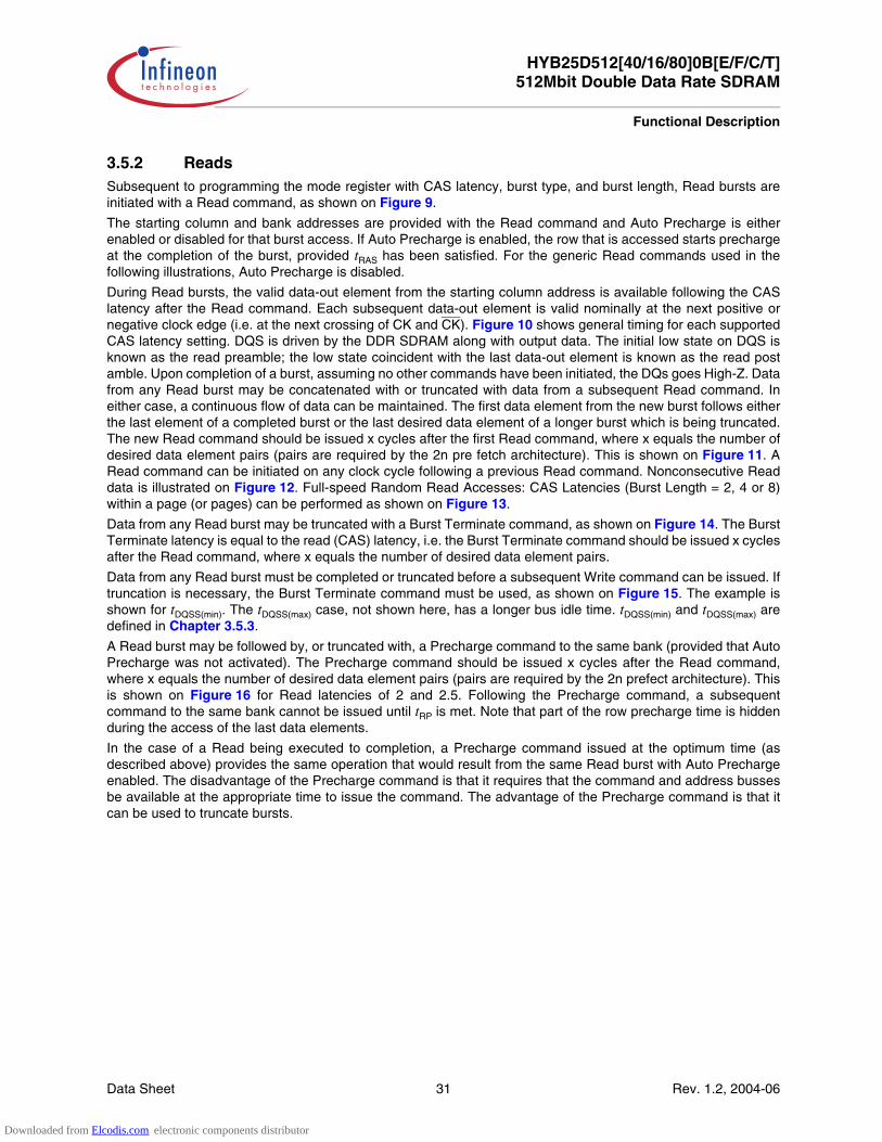
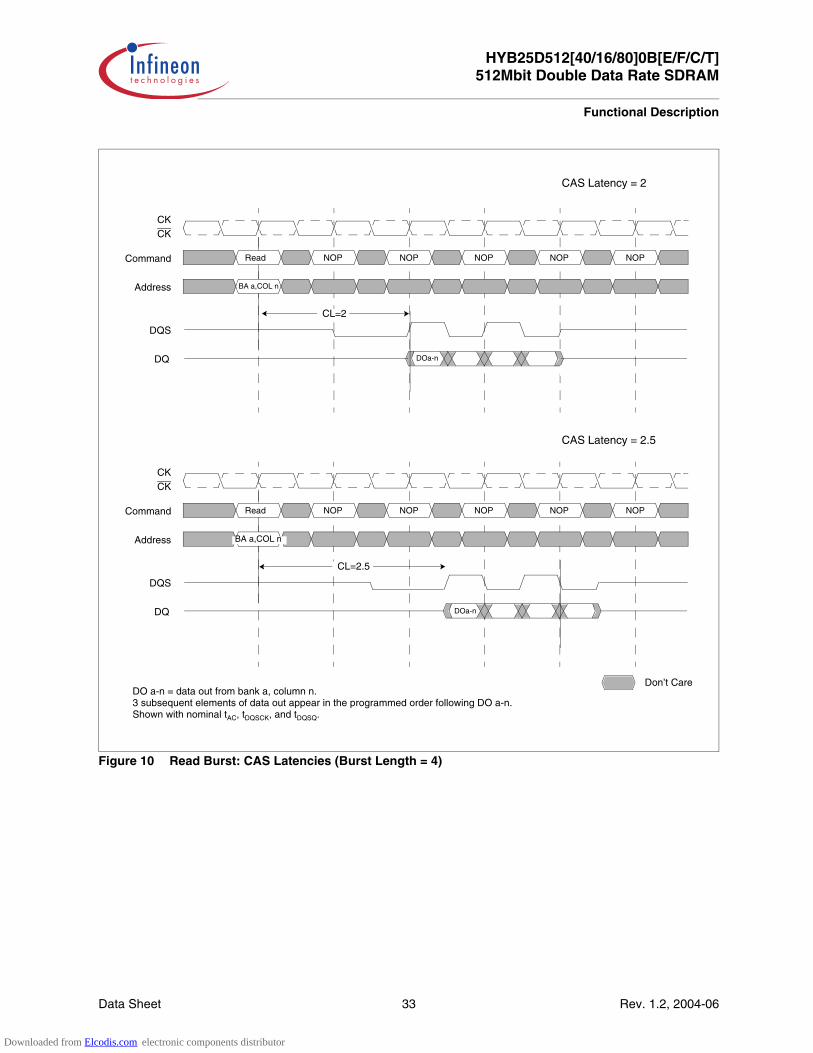
During Read bursts, the valid data-out element from the starting column address is available following the CASlatency after the Read command. Each subsequent data-out element is valid nominally at the next positive ornegative clock edge (i.e. at the next crossing of CK and CK). Figure 10 shows general timing for each supportedCAS latency setting. DQS is driven by the DDR SDRAM along with output data. The initial low state on DQS isknown as the read preamble; the low state coincident with the last data-out element is known as the read postamble. Upon completion of a burst, assuming no other commands have been initiated, the DQs goes High-Z. Datafrom any Read burst may be concatenated with or truncated with data from a subsequent Read command. Ineither case, a continuous flow of data can be maintained. The first data element from the new burst follows eitherthe last element of a completed burst or the last desired data element of a longer burst which is being truncated.The new Read command should be issued x cycles after the first Read command, where x equals the number ofdesired data element pairs (pairs are required by the 2n pre fetch architecture). This is shown on Figure 11. ARead command can be initiated on any clock cycle following a previous Read command. Nonconsecutive Readdata is illustrated on Figure 12. Full-speed Random Read Accesses: CAS Latencies (Burst Length = 2, 4 or 8)within a page (or pages) can be performed as shown on Figure 13.
Data from any Read burst may be truncated with a Burst Terminate command, as shown on Figure 14. The BurstTerminate latency is equal to the read (CAS) latency, i.e. the Burst Terminate command should be issued x cyclesafter the Read command, where x equals the number of desired data element pairs.
Data from any Read burst must be completed or truncated before a subsequent Write command can be issued. Iftruncation is necessary, the Burst Terminate command must be used, as shown on Figure 15. The example isshown for tDQSS(min). The tDQSS(max) case, not shown here, has a longer bus idle time. tDQSS(min) and tDQSS(max) aredefined in Chapter 3.5.3.
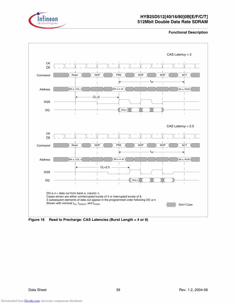
A Read burst may be followed by, or truncated with, a Precharge command to the same bank (provided that AutoPrecharge was not activated). The Precharge command should be issued x cycles after the Read command,where x equals the number of desired data element pairs (pairs are required by the 2n prefect architecture). Thisis shown on Figure 16 for Read latencies of 2 and 2.5. Following the Precharge command, a subsequentcommand to the same bank cannot be issued until tRP is met. Note that part of the row precharge time is hiddenduring the access of the last data elements.
In the case of a Read being executed to completion, a Precharge command issued at the optimum time (asdescribed above) provides the same operation that would result from the same Read burst with Auto Prechargeenabled. The disadvantage of the Precharge command is that it requires that the command and address bussesbe available at the appropriate time to issue the command. The advantage of the Precharge command is that itcan be used to truncate bursts.
Downloaded from Elcodis.com electronic components distributor

HYB25D512[40/16/80]0B[E/F/C/T]512Mbit Double Data Rate SDRAM
Functional Description
Data Sheet 32 Rev. 1.2, 2004-06
Figure 9 Read Command
BA
HIGH
CA = column addressBA = bank address
CKE
CS
RAS
CAS
WE
A10
BA0, BA1
Don’t Care
CAx4: A0-A9, A11
x8: A0-A9
EN AP
DIS AP
EN AP = enable Auto PrechargeDIS AP = disable Auto Precharge
CKCK
x16: A0-A8
Downloaded from Elcodis.com electronic components distributor
Data Sheet 33 Rev. 1.2, 2004-06
HYB25D512[40/16/80]0B[E/F/C/T]512Mbit Double Data Rate SDRAM
Functional Description
Figure 10 Read Burst: CAS Latencies (Burst Length = 4)
CAS Latency = 2
NOP NOP NOP NOP NOPRead
CKCK
Command
Address
DQS
DQ
CAS Latency = 2.5
Don’t Care
BA a,COL n
DOa-n
CL=2.5
NOP NOP NOP NOP NOPRead
CKCK
Command
Address
DQS
DQ
BA a,COL n
DOa-n
DO a-n = data out from bank a, column n.3 subsequent elements of data out appear in the programmed order following DO a-n.Shown with nominal tAC, tDQSCK, and tDQSQ.
CL=2
Downloaded from Elcodis.com electronic components distributor
HYB25D512[40/16/80]0B[E/F/C/T]512Mbit Double Data Rate SDRAM
Functional Description
Data Sheet 34 Rev. 1.2, 2004-06
Figure 11 Consecutive Read Bursts: CAS Latencies (Burst Length = 4 or 8)
CAS Latency = 2
NOP Read NOP NOP NOPRead
CKCK
Command
Address
DQS
DQ
CL=2
BAa, COL n BAa, COL b
Don’t CareDO a-n (or a-b) = data out from bank a, column n (or bank a, column b).When burst length = 4, the bursts are concatenated.When burst length = 8, the second burst interrupts the first.3 subsequent elements of data out appear in the programmed order following DO a-n.3 (or 7) subsequent elements of data out appear in the programmed order following DO a-b.Shown with nominal tAC, tDQSCK, and tDQSQ.
CAS Latency = 2.5
NOP Read NOP NOP NOPRead
CKCK
Command
Address
DQS
DQ
CL=2.5
BAa, COL n BAa,COL b
DOa-n
DOa- n DOa- b
DOa-b
Downloaded from Elcodis.com electronic components distributor

Data Sheet 35 Rev. 1.2, 2004-06
HYB25D512[40/16/80]0B[E/F/C/T]512Mbit Double Data Rate SDRAM
Functional Description
Figure 12 Non-Consecutive Read Bursts: CAS Latencies (Burst Length = 4)
CAS Latency = 2
NOP NOP Read NOP NOPRead
CKCK
Command
Address
DQS
DQ DO a-n DOa- b
DO a-n (or a-b) = data out from bank a, column n (or bank a, column b).3 subsequent elements of data out appear in the programmed order following DO a-n (and following DO a-b).Shown with nominal tAC, tDQSCK, and tDQSQ.
Don’t Care
BAa, COL n BAa, COL b
CL=2
CAS Latency = 2.5
NOP NOP Read NOP NOPRead
DO a-n DOa- b
BAa, COL n BAa, COL b
CL=2.5
CKCK
Command
Address
DQS
DQ
NOP
Downloaded from Elcodis.com electronic components distributor

HYB25D512[40/16/80]0B[E/F/C/T]512Mbit Double Data Rate SDRAM
Functional Description
Data Sheet 36 Rev. 1.2, 2004-06
Figure 13 Random Read Accesses: CAS Latencies (Burst Length = 2, 4 or 8)
DOa-n
CAS Latency = 2
Read Read Read NOP NOPRead
DOa-bDOa-n’ DOa-x DOa-x’ DOa-b’ DOa-g
CKCK
Command
Address
DQS
DQ
DO a-n, etc. = data out from bank a, column n etc.n' etc. = odd or even complement of n, etc. (i.e., column address LSB inverted).Reads are to active rows in any banks.Shown with nominal tAC, tDQSCK, and tDQSQ.
Don’t Care
BAa, COL n BAa, COL x BAa, COL b BAa, COL g
CL=2
CAS Latency = 2.5
Read Read Read NOP NOPRead
CKCK
Command
Address
DQS
DQ
BAa, COL n BAa, COL x BAa, COL b BAa, COL g
CL=2.5
DOa-n DOa-bDOa-n’ DOa-x DOa-x’ DOa-b’
Downloaded from Elcodis.com electronic components distributor

Data Sheet 37 Rev. 1.2, 2004-06
HYB25D512[40/16/80]0B[E/F/C/T]512Mbit Double Data Rate SDRAM
Functional Description
Figure 14 Terminating a Read Burst: CAS Latencies (Burst Length = 8)
CAS Latency = 2
NOP BST NOP NOP NOPRead
CK
Command
Address
DQS
DQ
DO a-n = data out from bank a, column n.Cases shown are bursts of 8 terminated after 4 data elements.3 subsequent elements of data out appear in the programmed order following DO a-n.Shown with nominal tAC, tDQSCK, and tDQSQ.
DOa-n
Don’t Care
CK
BAa, COL n
CL=2
CAS Latency = 2.5
NOP BST NOP NOP NOPRead
CK
Command
Address
DQS
DQ DOa-n
CK
BAa, COL n
CL=2.5
No further output data after this point.DQS tristated.
No further output data after this point.DQS tristated.
Downloaded from Elcodis.com electronic components distributor

HYB25D512[40/16/80]0B[E/F/C/T]512Mbit Double Data Rate SDRAM
Functional Description
Data Sheet 38 Rev. 1.2, 2004-06
Figure 15 Read to Write: CAS Latencies (Burst Length = 4 or 8)
CAS Latency = 2
BST NOP Write NOP NOPRead
DI a-b
CK
CK
Command
Address
DQS
DQ
DM
DOa-n
DO a-n = data out from bank a, column n
1 subsequent elements of data out appear in the programmed order following DO a-n.Data In elements are applied following Dl a-b in the programmed order, according to burst length.
Don’t Care
BAa, COL n BAa, COL b
CL=2 tDQSS (min)
CAS Latency = 2.5
BST NOP NOP Write NOPRead
CK
CK
Command
Address
DQS
DQ
DM
DOa-n
BAa, COL n BAa, COL b
CL=2.5 tDQSS (min)
Dla-b
Shown with nominal tAC, tDQSCK, and tDQSQ.
.DI a-b = data in to bank a, column b
Downloaded from Elcodis.com electronic components distributor
Data Sheet 39 Rev. 1.2, 2004-06
HYB25D512[40/16/80]0B[E/F/C/T]512Mbit Double Data Rate SDRAM
Functional Description
Figure 16 Read to Precharge: CAS Latencies (Burst Length = 4 or 8)
CAS Latency = 2
NOP PRE NOP NOP ACTRead
CK
CK
Command
Address
DQS
DQ DOa-n
DO a-n = data out from bank a, column n.Cases shown are either uninterrupted bursts of 4 or interrupted bursts of 8.3 subsequent elements of data out appear in the programmed order following DO a-n.Shown with nominal tAC, tDQSCK, and tDQSQ. Don’t Care
BA a, COL n BA a or all BA a, ROW
CL=2.5
CAS Latency = 2.5
NOP PRE NOP NOP ACTRead
CK
CK
Command
Address
DQS
DQ DOa-n
tRP
BA a, COL n BA a or all BA a, ROW
CL=2
tRP
Downloaded from Elcodis.com electronic components distributor
HYB25D512[40/16/80]0B[E/F/C/T]512Mbit Double Data Rate SDRAM
Functional Description
Data Sheet 40 Rev. 1.2, 2004-06
3.5.3 WritesWrite bursts are initiated with a Write command, as shown in Figure 17.
The starting column and bank addresses are provided with the Write command, and Auto Precharge is eitherenabled or disabled for that access. If Auto Precharge is enabled, the row being accessed is precharged at thecompletion of the burst. For the generic Write commands used in the following illustrations, Auto Precharge isdisabled.
During Write bursts, the first valid data-in element is registered on the first rising edge of DQS following the writecommand, and subsequent data elements are registered on successive edges of DQS. The Low state on DQSbetween the Write command and the first rising edge is known as the write preamble; the Low state on DQSfollowing the last data-in element is known as the write post amble. The time between the Write command and thefirst corresponding rising edge of DQS (tDQSS) is specified with a relatively wide range (from 75% to 125% of oneclock cycle), so most of the Write diagrams that follow are drawn for the two extreme cases (i.e. tDQSS(min) andtDQSS(max)). Figure 18 shows the two extremes of tDQSS for a burst of four. Upon completion of a burst, assumingno other commands have been initiated, the DQs and DQS enters High-Z and any additional input data is ignored.
Data for any Write burst may be concatenated with or truncated with a subsequent Write command. In either case,a continuous flow of input data can be maintained. The new Write command can be issued on any positive edgeof clock following the previous Write command. The first data element from the new burst is applied after eitherthe last element of a completed burst or the last desired data element of a longer burst which is being truncated.The new Write command should be issued x cycles after the first Write command, where x equals the number ofdesired data element pairs (pairs are required by the 2n pre fetch architecture). Figure 19 shows concatenatedbursts of 4. An example of non-consecutive Writes is shown in Figure 20. Full-speed random write accesseswithin a page or pages can be performed as shown in Figure 21. Data for any Write burst may be followed by asubsequent Read command. To follow a Write without truncating the write burst, tWTR (Write to Read) should bemet as shown in Figure 22.
Data for any Write burst may be truncated by a subsequent Read command, as shown in Figure 23 to Figure 25.Note that only the data-in pairs that are registered prior to the tWTR period are written to the internal array, and anysubsequent data-in must be masked with DM, as shown in the diagrams noted previously.
Data for any Write burst may be followed by a subsequent Precharge command. To follow a Write withouttruncating the write burst, tWR should be met as shown in Figure 26.
Data for any Write burst may be truncated by a subsequent Precharge command, as shown in Figure 27 toFigure 29. Note that only the data-in pairs that are registered prior to the tWR period are written to the internal array,and any subsequent data in should be masked with DM. Following the Precharge command, a subsequentcommand to the same bank cannot be issued until tRP is met.
In the case of a Write burst being executed to completion, a Precharge command issued at the optimum time (asdescribed above) provides the same operation that would result from the same burst with Auto Precharge. Thedisadvantage of the Precharge command is that it requires that the command and address busses be available atthe appropriate time to issue the command. The advantage of the Precharge command is that it can be used totruncate bursts.
Downloaded from Elcodis.com electronic components distributor
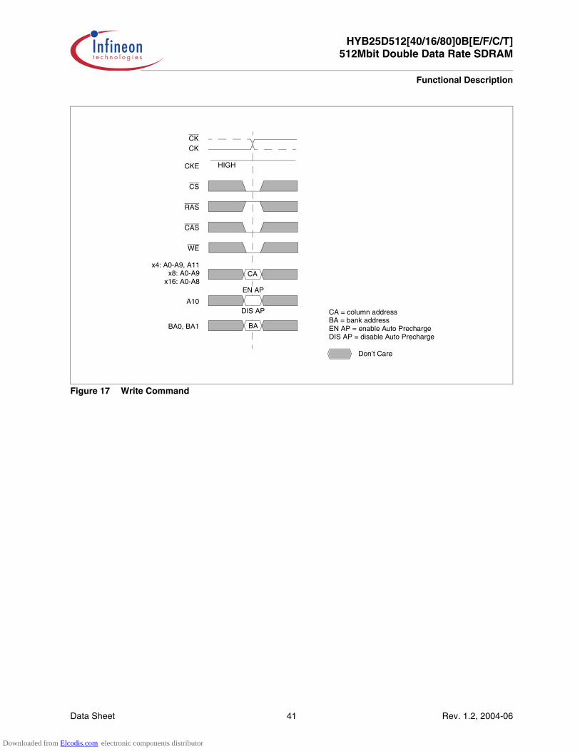
Data Sheet 41 Rev. 1.2, 2004-06
HYB25D512[40/16/80]0B[E/F/C/T]512Mbit Double Data Rate SDRAM
Functional Description
Figure 17 Write Command
BA
HIGH
CA = column addressBA = bank address
CKE
CS
RAS
CAS
WE
A10
BA0, BA1
Don’t Care
CAx4: A0-A9, A11
x8: A0-A9x16: A0-A8
EN AP
DIS AP
EN AP = enable Auto PrechargeDIS AP = disable Auto Precharge
CKCK
Downloaded from Elcodis.com electronic components distributor

HYB25D512[40/16/80]0B[E/F/C/T]512Mbit Double Data Rate SDRAM
Functional Description
Data Sheet 42 Rev. 1.2, 2004-06
Figure 18 Write Burst (Burst Length = 4)
T1 T2 T3 T4
tDQSS (max)
NOP NOP NOPWrite
DI a-b = data in for bank a, column b.3 subsequent elements of data in are applied in the programmed order following DI a-b.A non-interrupted burst is shown.A10 is Low with the Write command (Auto Precharge is disabled).
CK
CK
Command
Address
DQS
DQ
DM
Don’t Care
Maximum DQSS
BA a, COL b
T1 T2 T3 T4
tDQSS (min)
NOP NOP NOPWrite
CK
CK
Command
Address
DQS
Minimum DQSS
BA a, COL b
DQ
DM
Dla-b
Dla-b
Downloaded from Elcodis.com electronic components distributor

Data Sheet 43 Rev. 1.2, 2004-06
HYB25D512[40/16/80]0B[E/F/C/T]512Mbit Double Data Rate SDRAM
Functional Description
Figure 19 Write to Write (Burst Length = 4)
T1 T2 T3 T4 T5 T6
tDQSS (max)
Maximum DQSS
NOP Write NOP NOP NOPWrite
DI a-b = data in for bank a, column b, etc.3 subsequent elements of data in are applied in the programmed order following DI a-b.3 subsequent elements of data in are applied in the programmed order following DI a-n.A non-interrupted burst is shown.Each Write command may be to any bank.
CK
CK
Command
Address
DQS
DQ
DM
Don’t Care
T1 T2 T3 T4 T5 T6
Minimum DQSS
NOP Write NOP NOP NOPWrite
CK
CK
Command
Address
DQS
DQ
DM
BAa, COL b BAa, COL n
BA, COL b BA, COL n
tDQSS (min)
DI a-b DI a-n
DI a-b DI a-n
Downloaded from Elcodis.com electronic components distributor

HYB25D512[40/16/80]0B[E/F/C/T]512Mbit Double Data Rate SDRAM
Functional Description
Data Sheet 44 Rev. 1.2, 2004-06
Figure 20 Write to Write: Max. DQSS, Non-Consecutive (Burst Length = 4)
T1 T2 T3 T4 T5
tDQSS (max)
NOP NOP Write NOPWrite
DI a-b, etc. = data in for bank a, column b, etc.3 subsequent elements of data in are applied in the programmed order following DI a-b.3 subsequent elements of data in are applied in the programmed order following DI a-n.A non-interrupted burst is shown.Each Write command may be to any bank.
CK
CK
Command
Address
DQS
DQ
DM
Don’t Care
BAa, COL b BAa, COL n
DI a-b DI a-n
Downloaded from Elcodis.com electronic components distributor

Data Sheet 45 Rev. 1.2, 2004-06
HYB25D512[40/16/80]0B[E/F/C/T]512Mbit Double Data Rate SDRAM
Functional Description
Figure 21 Random Write Cycles (Burst Length = 2, 4 or 8)
T1 T2 T3 T4 T5
tDQSS (max)
Maximum DQSS
Write Write Write WriteWrite
DI a-b DI a-n
DI a-b, etc. = data in for bank a, column b, etc.b', etc. = odd or even complement of b, etc. (i.e., column address LSB inverted).Each Write command may be to any bank.
DI a-b’ DI a-x DI a-x’ DI a-n’ DI a-a DI a-a’
CK
CK
Command
Address
DQS
DQ
DM
Don’t Care
BAa, COL b BAa, COL x BAa, COL n BAa, COL a BAa, COL g
T1 T2 T3 T4 T5
Minimum DQSS
Write Write Write WriteWrite
DI a-b DI a-nDI a-b’ DI a-x DI a-x’ DI a-n’ DI a-a DI a-a’
CK
CK
Command
Address
DQS
DQ
DM
BAa, COL b BAa, COL x BAa, COL n BAa, COL a BAa, COL g
tDQSS (min)
DI a-g
Downloaded from Elcodis.com electronic components distributor
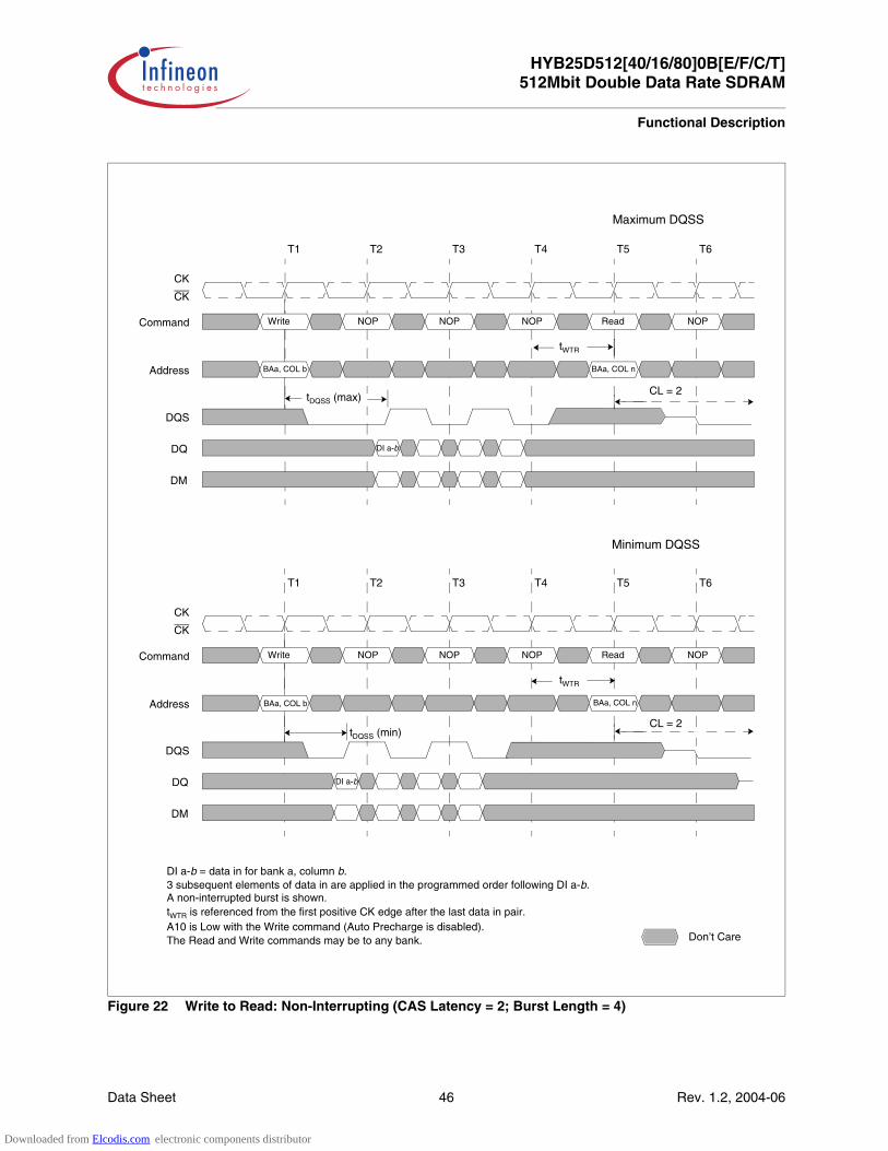
HYB25D512[40/16/80]0B[E/F/C/T]512Mbit Double Data Rate SDRAM
Functional Description
Data Sheet 46 Rev. 1.2, 2004-06
Figure 22 Write to Read: Non-Interrupting (CAS Latency = 2; Burst Length = 4)
CL = 2
T1 T2 T3 T4 T5 T6
tWTR
NOP NOP NOP ReadWrite
DI a-b
NOP
DI a-b = data in for bank a, column b.3 subsequent elements of data in are applied in the programmed order following DI a-b.A non-interrupted burst is shown.tWTR is referenced from the first positive CK edge after the last data in pair.A10 is Low with the Write command (Auto Precharge is disabled).The Read and Write commands may be to any bank.
CK
CK
Command
Address
DQS
DQ
DM
Don’t Care
Maximum DQSS
BAa, COL b BAa, COL n
T1 T2 T3 T4 T5 T6
tWTR
NOP NOP NOP ReadWrite NOP
CK
CK
Command
Address
Minimum DQSS
BAa, COL b BAa, COL n
tDQSS (max)
DI a-b
DQS
DQ
DM
tDQSS (min)
CL = 2
Downloaded from Elcodis.com electronic components distributor
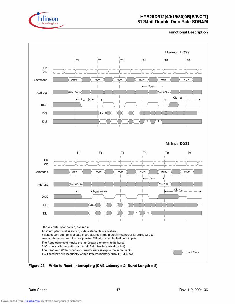
Data Sheet 47 Rev. 1.2, 2004-06
HYB25D512[40/16/80]0B[E/F/C/T]512Mbit Double Data Rate SDRAM
Functional Description
Figure 23 Write to Read: Interrupting (CAS Latency = 2; Burst Length = 8)
T1 T2 T3 T4 T5 T6
tDQSS (max)
Maximum DQSS
NOP NOP NOP ReadWrite NOP
DI a-b = data in for bank a, column b.An interrupted burst is shown, 4 data elements are written.3 subsequent elements of data in are applied in the programmed order following DI a-b.tWTR is referenced from the first positive CK edge after the last data in pair.
The Read command masks the last 2 data elements in the burst.A10 is Low with the Write command (Auto Precharge is disabled).The Read and Write commands are not necessarily to the same bank.
DIa- b
CK
CK
Command
Address
DQS
DQ
DM
Don’t Care
BAa, COL b BAa, COL n
tWTR
CL = 2
T1 T2 T3 T4 T5 T6
Minimum DQSS
NOP NOP NOP ReadWrite NOP
CK
CK
Command
Address BAa, COL b BAa, COL n
tWTR
DI a-b
DQS
DQ
DM
CL = 2tDQSS (min)
1 = These bits are incorrectly written into the memory array if DM is low.
1 1
1 1
Downloaded from Elcodis.com electronic components distributor

HYB25D512[40/16/80]0B[E/F/C/T]512Mbit Double Data Rate SDRAM
Functional Description
Data Sheet 48 Rev. 1.2, 2004-06
Minimum DQSS, Odd Number of Data (3-bit Write),Interrupting (CAS Latency = 2; Burst Length = 8)
Figure 24 Write to Read: Minimum DQSS, Odd Number of Data, Interupting
DI a-b = data in for bank a, column b.An interrupted burst is shown, 3 data elements are written.2 subsequent elements of data in are applied in the programmed order following DI a-b.tWTR is referenced from the first positive CK edge after the last desired data in pair (not the last desired data in element)The Read command masks the last 2 data elements in the burst.A10 is Low with the Write command (Auto Precharge is disabled).The Read and Write commands are not necessarily to the same bank.
Don’t Care
T1 T2 T3 T4 T5 T6
NOP NOP NOP ReadWrite NOP
CK
CK
Command
Address BAa, COL b BAa, COL n
tWTR
DI a-b
DQS
DQ
CL = 2tDQSS (min)
DM 1 2 2
1 = This bit is correctly written into the memory array if DM is low.2 = These bits are incorrectly written into the memory array if DM is low.
Downloaded from Elcodis.com electronic components distributor
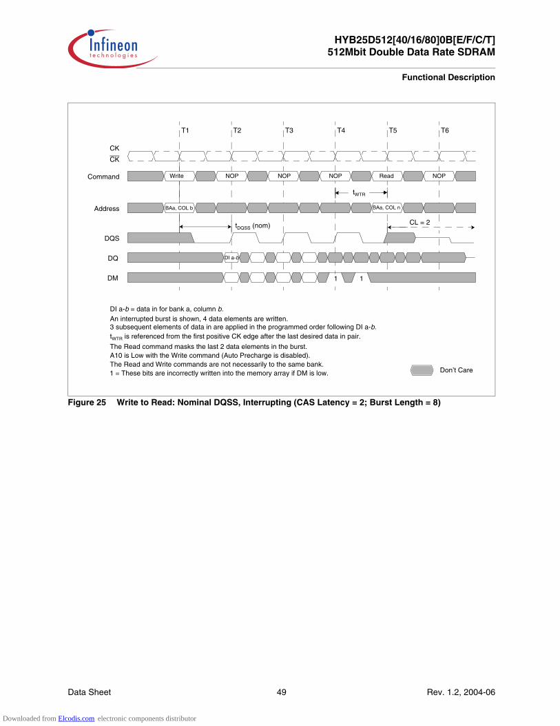
Data Sheet 49 Rev. 1.2, 2004-06
HYB25D512[40/16/80]0B[E/F/C/T]512Mbit Double Data Rate SDRAM
Functional Description
Figure 25 Write to Read: Nominal DQSS, Interrupting (CAS Latency = 2; Burst Length = 8)
T1 T2 T3 T4 T5 T6
tDQSS (nom)
NOP NOP NOP ReadWrite NOP
DI a-b = data in for bank a, column b.An interrupted burst is shown, 4 data elements are written.3 subsequent elements of data in are applied in the programmed order following DI a-b.tWTR is referenced from the first positive CK edge after the last desired data in pair.
The Read command masks the last 2 data elements in the burst.A10 is Low with the Write command (Auto Precharge is disabled).The Read and Write commands are not necessarily to the same bank.
DI a-b
CK
CK
Command
Address
DQS
DQ
DM
Don’t Care
BAa, COL b BAa, COL n
tWTR
CL = 2
1 = These bits are incorrectly written into the memory array if DM is low.
11
Downloaded from Elcodis.com electronic components distributor
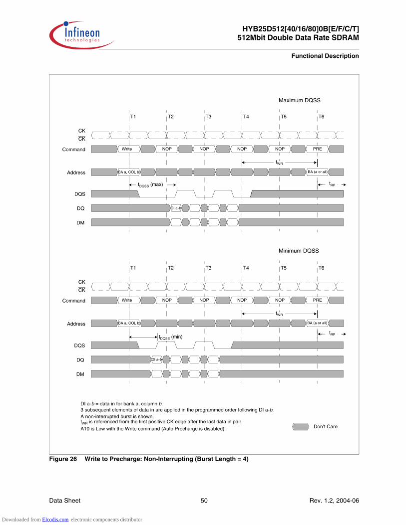
HYB25D512[40/16/80]0B[E/F/C/T]512Mbit Double Data Rate SDRAM
Functional Description
Data Sheet 50 Rev. 1.2, 2004-06
Figure 26 Write to Precharge: Non-Interrupting (Burst Length = 4)
T1 T2 T3 T4 T5 T6
tDQSS (max)
NOP NOP NOP NOPWrite
DI a-b
PRE
DI a-b = data in for bank a, column b.3 subsequent elements of data in are applied in the programmed order following DI a-b.A non-interrupted burst is shown.tWR is referenced from the first positive CK edge after the last data in pair.A10 is Low with the Write command (Auto Precharge is disabled).
CK
CK
Command
Address
DQS
DQ
DM
Don’t Care
BA a, COL b BA (a or all)
tWR
Maximum DQSS
T1 T2 T3 T4 T5 T6
NOP NOP NOP NOPWrite PRE
CK
CK
Command
Address BA a, COL b BA (a or all)
tWR
Minimum DQSS
DI a-b
DQS
DQ
DM
tDQSS (min)
tRP
tRP
Downloaded from Elcodis.com electronic components distributor

Data Sheet 51 Rev. 1.2, 2004-06
HYB25D512[40/16/80]0B[E/F/C/T]512Mbit Double Data Rate SDRAM
Functional Description
Figure 27 Write to Precharge: Interrupting (Burst Length = 4 or 8)
DI a-b = data in for bank a, column b.An interrupted burst is shown, 2 data elements are written.1 subsequent element of data in is applied in the programmed order following DI a-b.tWR is referenced from the first positive CK edge after the last desired data in pair.The Precharge command masks the last 2 data elements in the burst, for burst length = 8.
A10 is Low with the Write command (Auto Precharge is disabled).1 = Can be don't care for programmed burst length of 4.2 = For programmed burst length of 4, DQS becomes don't care at this point. Don’t Care
T1 T2 T3 T4 T5 T6
NOP NOP NOP PREWrite NOP
CK
CK
Command
Address
Maximum DQSS
DI a-b
1 1
2
DQS
DQ
DM
tDQSS (max) tRP
T1 T2 T3 T4 T5 T6
NOP NOP NOP PREWrite NOP
CK
CK
Command
Address BA a, COL b BA (a or all)
Minimum DQSS
tWR
tRP
DI a-b
1 1
DQS
DQ
DM
tDQSS (min) 2
BA a, COL b BA (a or all)
tWR
3 = These bits are incorrectly written into the memory array if DM is low.
33
33
Downloaded from Elcodis.com electronic components distributor
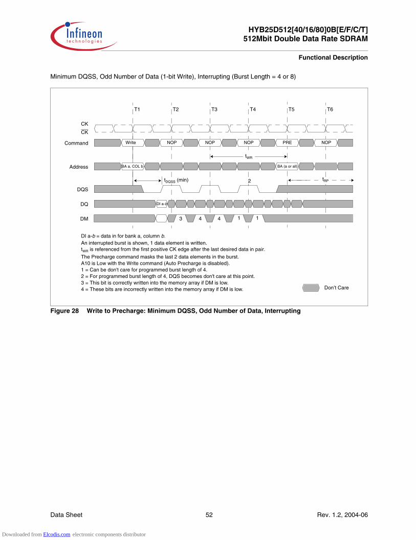
HYB25D512[40/16/80]0B[E/F/C/T]512Mbit Double Data Rate SDRAM
Functional Description
Data Sheet 52 Rev. 1.2, 2004-06
Minimum DQSS, Odd Number of Data (1-bit Write), Interrupting (Burst Length = 4 or 8)
Figure 28 Write to Precharge: Minimum DQSS, Odd Number of Data, Interrupting
DI a-b = data in for bank a, column b.An interrupted burst is shown, 1 data element is written.tWR is referenced from the first positive CK edge after the last desired data in pair.
The Precharge command masks the last 2 data elements in the burst.A10 is Low with the Write command (Auto Precharge is disabled).1 = Can be don't care for programmed burst length of 4.2 = For programmed burst length of 4, DQS becomes don't care at this point.
Don’t Care
T1 T2 T3 T4 T5 T6
NOP NOP NOP PREWrite NOP
CK
CK
Command
Address BA a, COL b BA (a or all)
tWR
tRP
DI a-b
DQS
DQ
tDQSS (min) 2
1 1DM 3 4 4
3 = This bit is correctly written into the memory array if DM is low.4 = These bits are incorrectly written into the memory array if DM is low.
Downloaded from Elcodis.com electronic components distributor
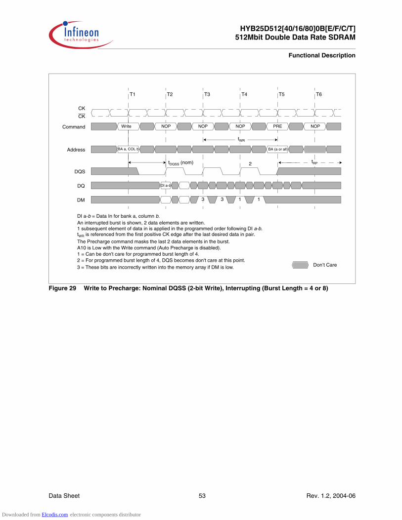
Data Sheet 53 Rev. 1.2, 2004-06
HYB25D512[40/16/80]0B[E/F/C/T]512Mbit Double Data Rate SDRAM
Functional Description
Figure 29 Write to Precharge: Nominal DQSS (2-bit Write), Interrupting (Burst Length = 4 or 8)
DI a-b = Data In for bank a, column b.An interrupted burst is shown, 2 data elements are written.1 subsequent element of data in is applied in the programmed order following DI a-b.tWR is referenced from the first positive CK edge after the last desired data in pair.
The Precharge command masks the last 2 data elements in the burst.A10 is Low with the Write command (Auto Precharge is disabled).1 = Can be don't care for programmed burst length of 4.2 = For programmed burst length of 4, DQS becomes don't care at this point.
Don’t Care
T1 T2 T3 T4 T5 T6
NOP NOP NOP PREWrite NOP
CK
CK
Command
Address BA a, COL b BA (a or all)
tRPtDQSS (nom)
DI a-b
1
2
DQS
DQ
DM 1
tWR
33
3 = These bits are incorrectly written into the memory array if DM is low.
Downloaded from Elcodis.com electronic components distributor

HYB25D512[40/16/80]0B[E/F/C/T]512Mbit Double Data Rate SDRAM
Functional Description
Data Sheet 54 Rev. 1.2, 2004-06
3.5.4 Pre chargeThe Pre charge command is used to deactivate the open row in a particular bank or the open row in all banks. Thebank(s) will be available for a subsequent row access some specified time (tRP) after the Pre charge command isissued. Input A10 determines whether one or all banks are to be pre charged, and in the case where only one bankis to be pre charged, inputs BA0, BA1 select the bank. When all banks are to be pre charged, inputs BA0, BA1 aretreated as “Don’t Care”. Once a bank has been pre charged, it is in the idle state and must be activated prior toany Read or Write commands being issued to that bank.
Figure 30 Precharge Command
BA
HIGH
BA = bank address
CKCK
CKE
CS
RAS
CAS
WE
A10
BA0, BA1
Don’t Care
All Banks
One Bank
(if A10 is Low, otherwise Don’t Care).
A0-A9, A11, A12
Downloaded from Elcodis.com electronic components distributor

Data Sheet 55 Rev. 1.2, 2004-06
HYB25D512[40/16/80]0B[E/F/C/T]512Mbit Double Data Rate SDRAM
Functional Description
3.5.5 Power-DownPower-down is entered when CKE is registered LOW (no accesses can be in progress). If power-down occurswhen all banks are idle, this mode is referred to as pre charge power-down; if power-down occurs when there isa row active in any bank, this mode is referred to as active power-down. Entering power-down deactivates theinput and output buffers, excluding CK, CK and CKE. The DLL is still running in Power Down mode, so formaximum power savings, the user has the option of disabling the DLL prior to entering Power-down. In that case,the DLL must be enabled after exiting power-down, and 200 clock cycles must occur before a Read command canbe issued. In power-down mode, CKE Low and a stable clock signal must be maintained at the inputs of the DDRSDRAM, and all other input signals are “Don’t Care”. However, power-down duration is limited by the refreshrequirements of the device, so in most applications, the self refresh mode is preferred over the DLL-disabledpower-down mode.
The power-down state is synchronously exited when CKE is registered HIGH (along with a NOP or Deselectcommand). A valid, executable command may be applied one clock cycle later.
Figure 31 Power Down
tIStIS
CK
CK
CKE
Command
No columnaccess inprogress
VALID NOP VALID
Don’t Care
Exitpower down
mode
Enter Power Down mode(Burst Read or Write operation
must not be in progress)
NOP
Downloaded from Elcodis.com electronic components distributor

HYB25D512[40/16/80]0B[E/F/C/T]512Mbit Double Data Rate SDRAM
Functional Description
Data Sheet 56 Rev. 1.2, 2004-06
Note:
1. CKEn is the logic state of CKE at clock edge n: CKE n-1 was the state of CKE at the previous clock edge.2. Current state is the state of the DDR SDRAM immediately prior to clock edge n.3. COMMAND n is the command registered at clock edge n, and ACTION n is a result of COMMAND n.4. All states and sequences not shown are illegal or reserved.
Table 10 Truth Table 2: Clock Enable (CKE)
Current State CKE n-1 CKEn Command n Action n Notes
PreviousCycle
CurrentCycle
Self Refresh L L X Maintain Self-Refresh 1)
Self Refresh L H Deselect or NOP Exit Self-Refresh 2)
Power Down L L X Maintain Power-Down –
Power Down L H Deselect or NOP Exit Power-Down –
All Banks Idle H L Deselect or NOP Precharge Power-Down Entry –
All Banks Idle H L AUTO REFRESH Self Refresh Entry –
Bank(s) Active H L Deselect or NOP Active Power-Down Entry –
H H See Table 11 – –
1) VREF must be maintained during Self Refresh operation
2) Deselect or NOP commands should be issued on any clock edges occurring during the Self Refresh Exit (tXSNR) period. Aminimum of 200 clock cycles are needed before applying a read command to allow the DLL to lock to the input clock.
Table 11 Truth Table 3: Current State Bank n - Command to Bank n (same bank)
Current State CS RAS CAS WE Command Action Notes
Any H X X X Deselect NOP. Continue previous operation. 1)2)3)4)5)6)
1) This table applies when CKE n-1 was HIGH and CKE n is HIGH (see Table 10 and after tXSNR/tXSRD has been met (if theprevious state was self refresh).
2) This table is bank-specific, except where noted, i.e., the current state is for a specific bank and the commands shown arethose allowed to be issued to that bank when in that state. Exceptions are covered in the notes below.
L H H H No Operation NOP. Continue previous operation. 1) to 6)
Idle L L H H Active Select and activate row 1) to 6)
L L L H AUTO REFRESH – 1) to 7)
L L L L MODE REGISTER SET
– 1) to 7)
Row Active L H L H Read Select column and start Read burst 1) to 6), 8)
L H L L Write Select column and start Write burst 1) to 6), 8)
L L H L Precharge Deactivate row in bank(s) 1) to 6), 9)
Read (Auto Precharge Disabled)
L H L H Read Select column and start new Read burst
1) to 6), 8)
L L H L Precharge Truncate Read burst, start Precharge
1) to 6), 9)
L H H L BURST TERMINATE
BURST TERMINATE 1) to 6), 10)
Write (Auto Precharge Disabled)
L H L H Read Select column and start Read burst 1) to 6), 8), 11)
L H L L Write Select column and start Write burst 1) to 6), 8)
L L H L Precharge Truncate Write burst, start Precharge 1) to 6), 9), 11)
Downloaded from Elcodis.com electronic components distributor
Data Sheet 57 Rev. 1.2, 2004-06
HYB25D512[40/16/80]0B[E/F/C/T]512Mbit Double Data Rate SDRAM
Functional Description
3) Current state definitions:Idle: The bank has been precharged, and tRP has been met.Row Active: A row in the bank has been activated, and tRCD has been met. No data bursts/accesses and no registeraccesses are in progress.Read: A Read burst has been initiated, with Auto Precharge disabled, and has not yet terminated or been terminated.Write: A Write burst has been initiated, with Auto Precharge disabled, and has not yet terminated or been terminated.
4) The following states must not be interrupted by a command issued to the same bank.Pre charging: Starts with registration of a Precharge command and ends when tRP is met. Once tRP is met, the bank is inthe idle state.Row Activating: Starts with registration of an Active command and ends when tRCD is met. Once tRCD is met, the bank is inthe “row active” state.Read w/Auto Precharge Enabled: Starts with registration of a Read command with Auto Precharge enabled and ends whentRP has been met. Once tRP is met, the bank is in the idle state.Write w/Auto Precharge Enabled: Starts with registration of a Write command with Auto Precharge enabled and ends whentRP has been met. Once tRP is met, the bank is in the idle state.Deselect or NOP commands, or allowable commands to the other bank should be issued on any clock edge occurringduring these states. Allowable commands to the other bank are determined by its current state and according to Table 12.
5) The following states must not be interrupted by any executable command; Deselect or NOP commands must be appliedon each positive clock edge during these states.Refreshing: Starts with registration of an Auto Refresh command and ends when tRFC is met. Once tRFC is met, the DDRSDRAM is in the “all banks idle” state.Accessing Mode Register: Starts with registration of a Mode Register Set command and ends when tMRD has been met.Once tMRD is met, the DDR SDRAM is in the “all banks idle” state.Pre charging All: Starts with registration of a Precharge All command and ends when tRP is met. Once tRP is met, all banksis in the idle state.
6) All states and sequences not shown are illegal or reserved.
7) Not bank-specific; requires that all banks are idle.
8) Reads or Writes listed in the Command/Action column include Reads or Writes with Auto Precharge enabled and Readsor Writes with Auto Precharge disabled.
9) May or may not be bank-specific; if all/any banks are to be precharged, all/any must be in a valid state for pre charging.
10) Not bank-specific; BURST TERMINATE affects the most recent Read burst, regardless of bank.
11) Requires appropriate DM masking.
Downloaded from Elcodis.com electronic components distributor

HYB25D512[40/16/80]0B[E/F/C/T]512Mbit Double Data Rate SDRAM
Functional Description
Data Sheet 58 Rev. 1.2, 2004-06
Table 12 Truth Table 4: Current State Bank n - Command to Bank m (different bank)
Current State CS RAS CAS WE Command Action Notes
Any H X X X Deselect NOP. Continue previous operation. 1)2)3)4)5)6)
L H H H No Operation NOP. Continue previous operation. 1) to 6)
Idle X X X X Any Command Otherwise Allowed to Bank m
– 1) to 6)
Row Activating, Active, or Pre charging
L L H H Active Select and activate row 1) to 6)
L H L H Read Select column and start Read burst 1) to 7)
L H L L Write Select column and start Write burst 1) to 7)
L L H L Precharge – 1) to 6)
Read (Auto Precharge Disabled)
L L H H Active Select and activate row 1) to 6)
L H L H Read Select column and start new Read burst
1) to 7)
L L H L Precharge – 1) to 6)
Write (Auto Precharge Disabled)
L L H H Active Select and activate row 1) to 6)
L H L H Read Select column and start Read burst 1) to 8)
L H L L Write Select column and start new Write burst
1) to 7)
L L H L Precharge – 1) to 6)
Read (With Auto Precharge)
L L H H Active Select and activate row 1) to 6)
L H L H Read Select column and start new Read burst
1) to 7), 9)
L H L L Write Select column and start Write burst 1) to 7), 9), 10)
L L H L Precharge – 1) to 6)
Write (With Auto Precharge)
L L H H Active Select and activate row 1) to 6)
L H L H Read Select column and start Read burst 1) to 7), 9)
L H L L Write Select column and start new Write burst
1) to 7), 9)
L L H L Precharge – 1) to 6)
1) This table applies when CKE n-1 was HIGH and CKE n is HIGH (see Table 10: Clock Enable (CKE) and after tXSNR/tXSRDhas been met (if the previous state was self refresh).
2) This table describes alternate bank operation, except where noted, i.e., the current state is for bank n and the commandsshown are those allowed to be issued to bank m (assuming that bank m is in such a state that the given command isallowable). Exceptions are covered in the notes below.
3) Current state definitions:Idle: The bank has been precharged, and tRP has been met.Row Active: A row in the bank has been activated, and tRCD has been met. No data bursts/accesses and no registeraccesses are in progress.Read: A Read burst has been initiated, with Auto Precharge disabled, and has not yet terminated or been terminated.Write: A Write burst has been initiated, with Auto Precharge disabled, and has not yet terminated or been terminated.Read with Auto Precharge Enabled: See 10).Write with Auto Precharge Enabled: See 10).
4) AUTO REFRESH and Mode Register Set commands may only be issued when all banks are idle.
5) A BURST TERMINATE command cannot be issued to another bank; it applies to the bank represented by the current stateonly.
6) All states and sequences not shown are illegal or reserved.
Downloaded from Elcodis.com electronic components distributor
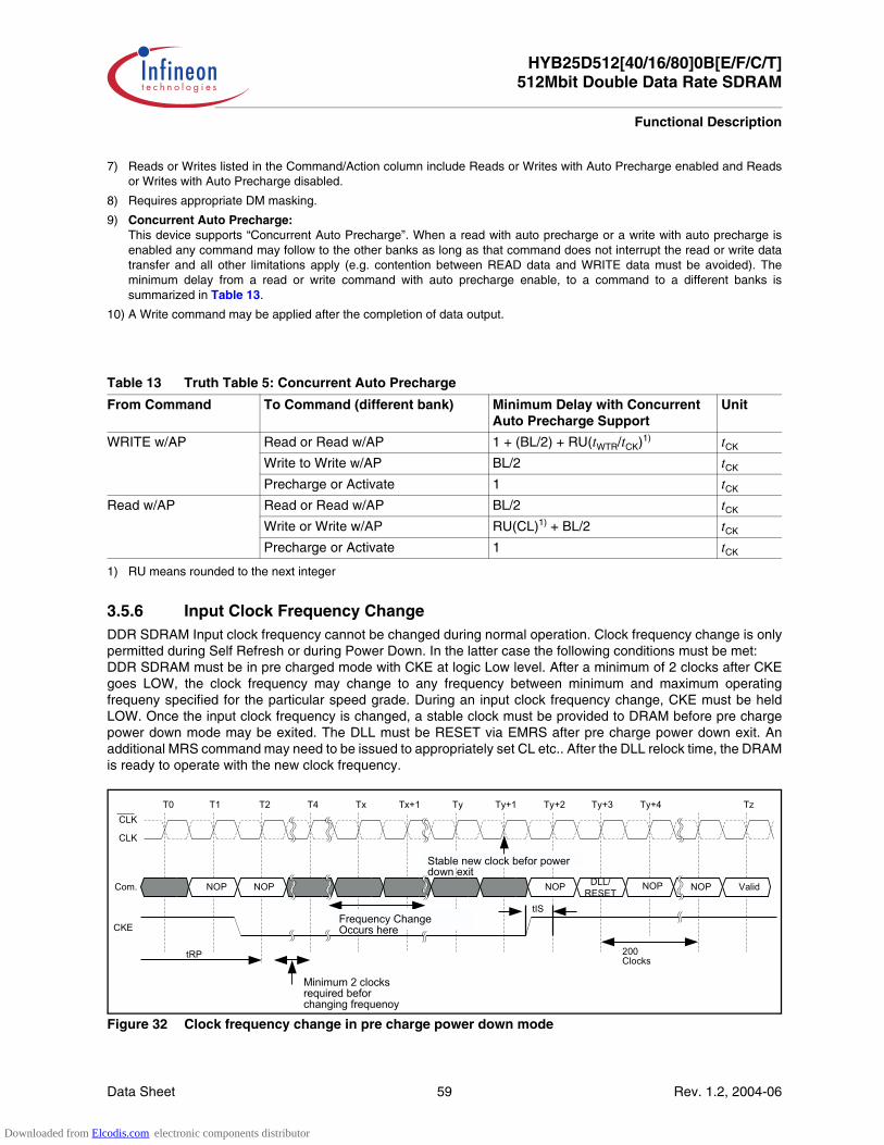
Data Sheet 59 Rev. 1.2, 2004-06
HYB25D512[40/16/80]0B[E/F/C/T]512Mbit Double Data Rate SDRAM
Functional Description
3.5.6 Input Clock Frequency ChangeDDR SDRAM Input clock frequency cannot be changed during normal operation. Clock frequency change is onlypermitted during Self Refresh or during Power Down. In the latter case the following conditions must be met:DDR SDRAM must be in pre charged mode with CKE at logic Low level. After a minimum of 2 clocks after CKEgoes LOW, the clock frequency may change to any frequency between minimum and maximum operatingfrequeny specified for the particular speed grade. During an input clock frequency change, CKE must be heldLOW. Once the input clock frequency is changed, a stable clock must be provided to DRAM before pre chargepower down mode may be exited. The DLL must be RESET via EMRS after pre charge power down exit. Anadditional MRS command may need to be issued to appropriately set CL etc.. After the DLL relock time, the DRAMis ready to operate with the new clock frequency.
Figure 32 Clock frequency change in pre charge power down mode
7) Reads or Writes listed in the Command/Action column include Reads or Writes with Auto Precharge enabled and Readsor Writes with Auto Precharge disabled.
8) Requires appropriate DM masking.
9) Concurrent Auto Precharge:This device supports “Concurrent Auto Precharge”. When a read with auto precharge or a write with auto precharge isenabled any command may follow to the other banks as long as that command does not interrupt the read or write datatransfer and all other limitations apply (e.g. contention between READ data and WRITE data must be avoided). Theminimum delay from a read or write command with auto precharge enable, to a command to a different banks issummarized in Table 13.
10) A Write command may be applied after the completion of data output.
Table 13 Truth Table 5: Concurrent Auto Precharge
From Command To Command (different bank) Minimum Delay with Concurrent Auto Precharge Support
Unit
WRITE w/AP Read or Read w/AP 1 + (BL/2) + RU(tWTR/tCK)1)
1) RU means rounded to the next integer
tCK
Write to Write w/AP BL/2 tCK
Precharge or Activate 1 tCK
Read w/AP Read or Read w/AP BL/2 tCK
Write or Write w/AP RU(CL)1) + BL/2 tCK
Precharge or Activate 1 tCK
$%
& & & & &# &#' &( &('
)
&*&(' &(' &('
++ +
&+ + ,-./0
/1/%2%!!3.$3456782/670!"79$63:-1;/1;!9678271$(
6782713(!:-1;7+33265!:767
)<
.$345
)-".7!17=!3.$34!"79$6!>$=760$=1!7#/)
Downloaded from Elcodis.com electronic components distributor

HYB25D512[40/16/80]0B[E/F/C/T]512Mbit Double Data Rate SDRAM
Functional Description
Data Sheet 60 Rev. 1.2, 2004-06
3.6 Simplified State Diagram
Figure 33 Simplified State Diagram
Self
AutoIdle
MRSEMRS
Row
Precharge
Power
Write
Power
ACT
Read A
Read
REFS
REFSX
REFA
CKEL
MRS
CKEH
CKEH
CKEL
Write
PowerApplied
Automatic Sequence
Command Sequence
Read AWrite A
Read
PRE PRE
PRE
PRE
Refresh
Refresh
Down
PowerDown
Active
On
A
ReadA
ReadA
Write A
Burst Stop
PREALL
Active
Precharge
PrechargePREALL
ReadWrite
PREALL = Precharge All BanksMRS = Mode Register SetEMRS = Extended Mode Register SetREFS = Enter Self RefreshREFSX = Exit Self RefreshREFA = Auto Refresh
CKEL = Enter Power DownCKEH = Exit Power DownACT = ActiveWrite A = Write with AutoprechargeRead A = Read with AutoprechargePRE = Precharge
Downloaded from Elcodis.com electronic components distributor

Data Sheet 61 Rev. 1.2, 2004-06
HYB25D512[40/16/80]0B[E/F/C/T]512Mbit Double Data Rate SDRAM
Electrical Characteristics
4 Electrical Characteristics
4.1 Operating Conditions
Attention: Permanent damage to the device may occur if “Absolute Maximum Ratings” are exceeded. Thisis a stress rating only, and functional operation should be restricted to recommended operationconditions. Exposure to absolute maximum rating conditions for extended periods of time mayaffect device reliability and exceeding only one of the values may cause irreversible damage tothe integrated circuit.
Table 14 Absolute Maximum Ratings
Parameter Symbol Values Unit Note/ Test Conditionmin. typ. max.
Voltage on I/O pins relative to VSS VIN, VOUT –0.5 – VDDQ +0.5
V –
Voltage on inputs relative to VSS VIN –1 – +3.6 V –
Voltage on VDD supply relative to VSS VDD –1 – +3.6 V –
Voltage on VDDQ supply relative to VSS VDDQ –1 – +3.6 V –
Operating temperature (ambient) TA 0 – +70 °C –
Storage temperature (plastic) TSTG -55 – +150 °C –
Power dissipation (per SDRAM component) PD – 1 – W –
Short circuit output current IOUT – 50 – mA –
Table 15 Input and Output Capacitances
Parameter Symbol Values Unit Note/ Test ConditionMin. Typ. Max.
Input Capacitance: CK, CK CI1 1.5 — 2.5 pF TSOPII 1)
1) These values are guaranteed by design and are tested on a sample base only. VDDQ = VDD = 2.5 V ± 0.2 V, f = 100 MHz,TA = 25 °C, VOUT(DC) = VDDQ/2, VOUT (Peak to Peak) 0.2 V. Unused pins are tied to ground.
2.0 — 3.0 pF TFBGA 1)
Delta Input Capacitance CdI1 — — 0.25 pF 1)
Input Capacitance:All other input-only pins
CI2 1.5 — 2.5 pF TFBGA 1)
2.0 — 3.0 pF TSOPII 1)
Delta Input Capacitance:All other input-only pins
CdIO — — 0.5 pF 1)
Input/Output Capacitance: DQ, DQS, DM CIO 3.5 — 4.5 pF TFBGA 1)2)
2) DM inputs are grouped with I/O pins reflecting the fact that they are matched in loading to DQ and DQS to facilitate tracematching at the board level.
4.0 — 5.0 pF TSOPII 1)2)
Delta Input/Output Capacitance:DQ, DQS, DM
CdIO — — 0.5 pF 1)
Downloaded from Elcodis.com electronic components distributor

Data Sheet 62 Rev. 1.2, 2004-06
HYB25D512[40/16/80]0B[E/F/C/T]512Mbit Double Data Rate SDRAM
Electrical Characteristics
Electrical Characteristics and DC Operating Conditions
Parameter Symbol Values Unit Note/Test Condition 1)
1) 0 °C ≤ TA ≤ 70 °C; VDDQ = 2.5 V ± 0.2 V, VDD = +2.5 V ± 0.2 V; VDDQ = 2.6 V ± 0.1 V, VDD = +2.6 V ± 0.1 V (DDR400);
Min. Typ. Max.
Device Supply Voltage VDD 2.3 2.5 2.7 V fCK ≤ 166 MHz
Device Supply Voltage VDD 2.5 2.6 2.7 V fCK > 166 MHz 2)
2) DDR400 conditions apply for all clock frequencies above 166 MHz
Output Supply Voltage VDDQ 2.3 2.5 2.7 V fCK ≤ 166 MHz 3)
3) Under all conditions, VDDQ must be less than or equal to VDD.
Output Supply Voltage VDDQ 2.5 2.6 2.7 V fCK > 166 MHz 2)3)
Supply Voltage, I/O Supply Voltage
VSS, VSSQ
0 0 V —
Input Reference Voltage VREF 0.49 × VDDQ
0.5 × VDDQ
0.51 × VDDQ
V 4)
4) Peak to peak AC noise on VREF may not exceed ± 2% VREF (DC). VREF is also expected to track noise variations in VDDQ.
I/O Termination Voltage (System)
VTT VREF – 0.04 VREF + 0.04 V 5)
5) VTT is not applied directly to the device. VTT is a system supply for signal termination resistors, is expected to be set equalto VREF, and must track variations in the DC level of VREF.
Input High (Logic1) Voltage VIH(DC) VREF + 0.15 VDDQ + 0.3 V 6)
6) Inputs are not recognized as valid until VREF stabilizes.
Input Low (Logic0) Voltage VIL(DC) –0.3 VREF – 0.15 V 6)
Input Voltage Level, CK and CK Inputs
VIN(DC) –0.3 VDDQ + 0.3 V 6)
Input Differential Voltage, CK and CK Inputs
VID(DC) 0.36 VDDQ + 0.6 V 6)7)
7) VID is the magnitude of the difference between the input level on CK and the input level on CK.
VI-Matching Pull-up Current to Pull-down Current
VIRatio 0.71 1.4 — 8)
8) The ratio of the pull-up current to the pull-down current is specified for the same temperature and voltage, over the entiretemperature and voltage range, for device drain to source voltage from 0.25 to 1.0 V. For a given output, it represents themaximum difference between pull-up and pull-down drivers due to process variation.
Input Leakage Current II –2 2 µA Any input 0 V ≤ VIN ≤ VDD; All other pins not under test = 0 V 9)
9) Values are shown per pin.
Output Leakage Current IOZ –5 5 µA DQs are disabled; 0 V ≤ VOUT ≤ VDDQ 9)
Output High Current, Normal Strength Driver
IOH — –16.2 mA VOUT = 1.95 V
Output Low Current, Normal Strength Driver
IOL 16.2 — mA VOUT = 0.35 V
Downloaded from Elcodis.com electronic components distributor

Data Sheet 63 Rev. 1.2, 2004-06
HYB25D512[40/16/80]0B[E/F/C/T]512Mbit Double Data Rate SDRAM
Normal Strength Pull-down and Pull-up Characteristics
5 Normal Strength Pull-down and Pull-up Characteristics1. The nominal pull-down V-I curve for DDR SDRAM devices is expected, but not guaranteed, to lie within the
inner bounding lines of the V-I curve.2. The full variation in driver pull-down current from minimum to maximum process, temperature, and voltage lie
within the outer bounding lines of the V-I curve.3. The nominal pull-up V-I curve for DDR SDRAM devices is expected, but not guaranteed, to lie within the inner
bounding lines of the V-I curve.4. The full variation in driver pull-up current from minimum to maximum process, temperature, and voltage lie
within the outer bounding lines of the V-I curve.5. The full variation in the ratio of the maximum to minimum pull-up and pull-down current does not exceed 1.7,
for device drain to source voltages from 0.1 to 1.0.6. The full variation in the ratio of the nominal pull-up to pull-down current should be unity ±10%, for device drain
to source voltages from 0.1 to 1.0 V.
Figure 34 Normal Strength Pull-down Characteristics
Figure 35 Normal Strength Pull-up Characteristics
00.5 1 1.5 2 2.50
20
40
60
80
100
120
140
I OU
T (
mA
)
VDDQ - VOUT (V)
Maximum
Nominal High
Nominal Low
Minimum
Maximum
Nominal High
Nominal Low
Minimum
VDDQ - VOUT (V)0.5 1 1.5 2 2.50
0
-20
-40
-60
-80
-100
-120
-140
-160
I OU
T (
mA
)
Downloaded from Elcodis.com electronic components distributor
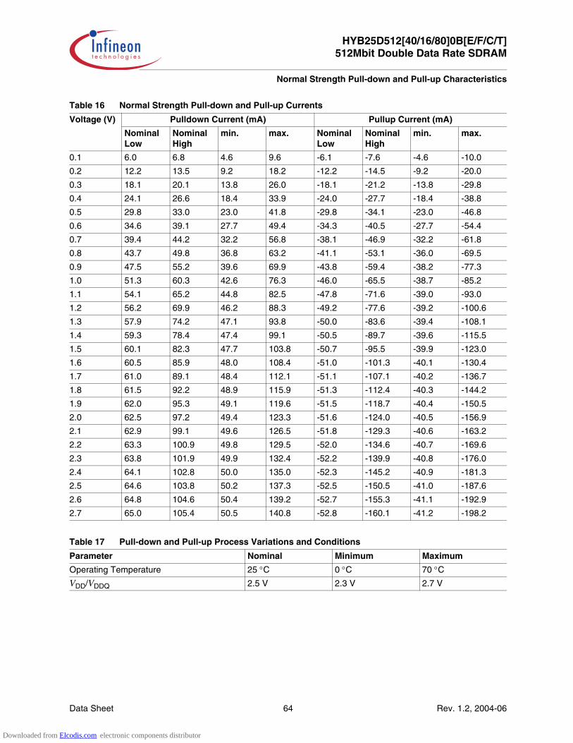
Data Sheet 64 Rev. 1.2, 2004-06
HYB25D512[40/16/80]0B[E/F/C/T]512Mbit Double Data Rate SDRAM
Normal Strength Pull-down and Pull-up Characteristics
Table 16 Normal Strength Pull-down and Pull-up Currents
Voltage (V) Pulldown Current (mA) Pullup Current (mA)
Nominal Low
Nominal High
min. max. Nominal Low
Nominal High
min. max.
0.1 6.0 6.8 4.6 9.6 -6.1 -7.6 -4.6 -10.0
0.2 12.2 13.5 9.2 18.2 -12.2 -14.5 -9.2 -20.0
0.3 18.1 20.1 13.8 26.0 -18.1 -21.2 -13.8 -29.8
0.4 24.1 26.6 18.4 33.9 -24.0 -27.7 -18.4 -38.8
0.5 29.8 33.0 23.0 41.8 -29.8 -34.1 -23.0 -46.8
0.6 34.6 39.1 27.7 49.4 -34.3 -40.5 -27.7 -54.4
0.7 39.4 44.2 32.2 56.8 -38.1 -46.9 -32.2 -61.8
0.8 43.7 49.8 36.8 63.2 -41.1 -53.1 -36.0 -69.5
0.9 47.5 55.2 39.6 69.9 -43.8 -59.4 -38.2 -77.3
1.0 51.3 60.3 42.6 76.3 -46.0 -65.5 -38.7 -85.2
1.1 54.1 65.2 44.8 82.5 -47.8 -71.6 -39.0 -93.0
1.2 56.2 69.9 46.2 88.3 -49.2 -77.6 -39.2 -100.6
1.3 57.9 74.2 47.1 93.8 -50.0 -83.6 -39.4 -108.1
1.4 59.3 78.4 47.4 99.1 -50.5 -89.7 -39.6 -115.5
1.5 60.1 82.3 47.7 103.8 -50.7 -95.5 -39.9 -123.0
1.6 60.5 85.9 48.0 108.4 -51.0 -101.3 -40.1 -130.4
1.7 61.0 89.1 48.4 112.1 -51.1 -107.1 -40.2 -136.7
1.8 61.5 92.2 48.9 115.9 -51.3 -112.4 -40.3 -144.2
1.9 62.0 95.3 49.1 119.6 -51.5 -118.7 -40.4 -150.5
2.0 62.5 97.2 49.4 123.3 -51.6 -124.0 -40.5 -156.9
2.1 62.9 99.1 49.6 126.5 -51.8 -129.3 -40.6 -163.2
2.2 63.3 100.9 49.8 129.5 -52.0 -134.6 -40.7 -169.6
2.3 63.8 101.9 49.9 132.4 -52.2 -139.9 -40.8 -176.0
2.4 64.1 102.8 50.0 135.0 -52.3 -145.2 -40.9 -181.3
2.5 64.6 103.8 50.2 137.3 -52.5 -150.5 -41.0 -187.6
2.6 64.8 104.6 50.4 139.2 -52.7 -155.3 -41.1 -192.9
2.7 65.0 105.4 50.5 140.8 -52.8 -160.1 -41.2 -198.2
Table 17 Pull-down and Pull-up Process Variations and Conditions
Parameter Nominal Minimum Maximum
Operating Temperature 25 °C 0 °C 70 °C
VDD/VDDQ 2.5 V 2.3 V 2.7 V
Downloaded from Elcodis.com electronic components distributor

Data Sheet 65 Rev. 1.2, 2004-06
HYB25D512[40/16/80]0B[E/F/C/T]512Mbit Double Data Rate SDRAM
Normal Strength Pull-down and Pull-up Characteristics
5.1 Weak Strength Pull-down and Pull-up Characteristics
1. The weak pull-down V-I curve for DDR SDRAM devices is expected, but not guaranteed, to lie within the innerbounding lines of the V-I curve.
2. The weak pull-up V-I curve for DDR SDRAM devices is expected, but not guaranteed, to lie within the innerbounding lines of the V-I curve.
3. The full variation in driver pull-up current from minimum to maximum process, temperature, and voltage liewithin the outer bounding lines of the V-I curve.
4. The full variation in the ratio of the maximum to minimum pull-up and pull-down current does not exceed 1.7,for device drain to source voltages from 0.1 to 1.0.
5. The full variation in the ratio of the nominal pull-up to pull-down current should be unity ±10%, for device drainto source voltages from 0.1 to 1.0 V.
Figure 36 Weak Strength Pull-down Characteristics
Figure 37 Weak Strength Pull-up Characteristics
0
10
20
30
40
50
60
70
80
0,0 0,5 1,0 1,5 2,0 2,5
Vout [V]
Iout
[mA
]
Maximum
Typical high
Typical low
Minimum
-80,0
-70,0
-60,0
-50,0
-40,0
-30,0
-20,0
-10,0
0,00,0 0,5 1,0 1,5 2,0 2,5
Vout [V]
Iout
[V]
Maximum
Typical high
Typical low
Minimum
Downloaded from Elcodis.com electronic components distributor
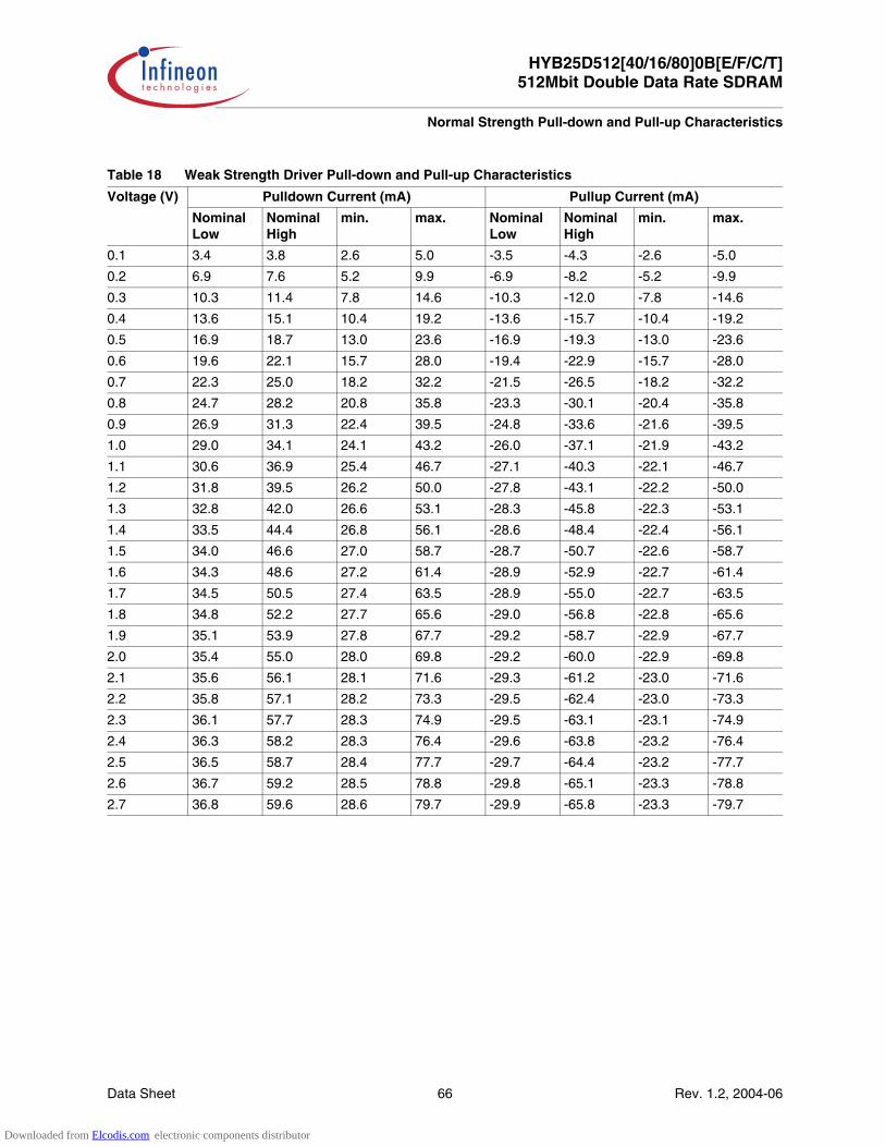
Data Sheet 66 Rev. 1.2, 2004-06
HYB25D512[40/16/80]0B[E/F/C/T]512Mbit Double Data Rate SDRAM
Normal Strength Pull-down and Pull-up Characteristics
Table 18 Weak Strength Driver Pull-down and Pull-up Characteristics
Voltage (V) Pulldown Current (mA) Pullup Current (mA)
Nominal Low
Nominal High
min. max. Nominal Low
Nominal High
min. max.
0.1 3.4 3.8 2.6 5.0 -3.5 -4.3 -2.6 -5.0
0.2 6.9 7.6 5.2 9.9 -6.9 -8.2 -5.2 -9.9
0.3 10.3 11.4 7.8 14.6 -10.3 -12.0 -7.8 -14.6
0.4 13.6 15.1 10.4 19.2 -13.6 -15.7 -10.4 -19.2
0.5 16.9 18.7 13.0 23.6 -16.9 -19.3 -13.0 -23.6
0.6 19.6 22.1 15.7 28.0 -19.4 -22.9 -15.7 -28.0
0.7 22.3 25.0 18.2 32.2 -21.5 -26.5 -18.2 -32.2
0.8 24.7 28.2 20.8 35.8 -23.3 -30.1 -20.4 -35.8
0.9 26.9 31.3 22.4 39.5 -24.8 -33.6 -21.6 -39.5
1.0 29.0 34.1 24.1 43.2 -26.0 -37.1 -21.9 -43.2
1.1 30.6 36.9 25.4 46.7 -27.1 -40.3 -22.1 -46.7
1.2 31.8 39.5 26.2 50.0 -27.8 -43.1 -22.2 -50.0
1.3 32.8 42.0 26.6 53.1 -28.3 -45.8 -22.3 -53.1
1.4 33.5 44.4 26.8 56.1 -28.6 -48.4 -22.4 -56.1
1.5 34.0 46.6 27.0 58.7 -28.7 -50.7 -22.6 -58.7
1.6 34.3 48.6 27.2 61.4 -28.9 -52.9 -22.7 -61.4
1.7 34.5 50.5 27.4 63.5 -28.9 -55.0 -22.7 -63.5
1.8 34.8 52.2 27.7 65.6 -29.0 -56.8 -22.8 -65.6
1.9 35.1 53.9 27.8 67.7 -29.2 -58.7 -22.9 -67.7
2.0 35.4 55.0 28.0 69.8 -29.2 -60.0 -22.9 -69.8
2.1 35.6 56.1 28.1 71.6 -29.3 -61.2 -23.0 -71.6
2.2 35.8 57.1 28.2 73.3 -29.5 -62.4 -23.0 -73.3
2.3 36.1 57.7 28.3 74.9 -29.5 -63.1 -23.1 -74.9
2.4 36.3 58.2 28.3 76.4 -29.6 -63.8 -23.2 -76.4
2.5 36.5 58.7 28.4 77.7 -29.7 -64.4 -23.2 -77.7
2.6 36.7 59.2 28.5 78.8 -29.8 -65.1 -23.3 -78.8
2.7 36.8 59.6 28.6 79.7 -29.9 -65.8 -23.3 -79.7
Downloaded from Elcodis.com electronic components distributor

Data Sheet 67 Rev. 1.2, 2004-06
HYB25D512[40/16/80]0B[E/F/C/T]512Mbit Double Data Rate SDRAM
Normal Strength Pull-down and Pull-up Characteristics
5.2 AC Characteristics
(Notes 1-5 apply to the following Tables; Electrical Characteristics and DC Operating Conditions, AC OperatingConditions, IDD Specifications and Conditions, and Electrical Characteristics and AC Timing.)
Note:
1. All voltages referenced to VSS.2. Tests for AC timing, IDD, and electrical, AC and DC characteristics, may be conducted at nominal reference/
supply voltage levels, but the related specifications and device operation are guaranteed for the full voltagerange specified.
3. Figure 38 represents the timing reference load used in defining the relevant timing parameters of the part. Itis not intended to be either a precise representation of the typical system environment nor a depiction of theactual load presented by a production tester. System designers will use IBIS or other simulation tools tocorrelate the timing reference load to a system environment. Manufacturers will correlate to their productiontest conditions (generally a coaxial transmission line terminated at the tester electronics).
4. AC timing and IDD tests may use a VIL to VIH swing of up to 1.5 V in the test environment, but input timing isstill referenced to VREF (or to the crossing point for CK, CK), and parameter specifications are guaranteed forthe specified AC input levels under normal use conditions. The minimum slew rate for the input signals is 1 V/ns in the range between VIL(AC) and VIH(AC).
5. The AC and DC input level specifications are as defined in the SSTL_2 Standard (i.e. the receiver effectivelyswitches as a result of the signal crossing the AC input level, and remains in that state as long as the signaldoes not ring back above (below) the DC input LOW (HIGH) level).
6. For System Characteristics like Setup & Holdtime Derating for Slew Rate, I/O Delta Rise/Fall Derating, DDRSDRAM Slew Rate Standards, Overshoot & Undershoot specification and Clamp V-I characteristics see thelatest JEDEC specification for DDR components.
Figure 38 AC Output Load Circuit Diagram / Timing Reference Load
AC Timing - Absolute Specifications for PC3200, PC2700 and PC2100
Parameter Symbol –5 –6 –7 Unit Note/ TestCondition 1)DDR400B DDR333 DDR266A
Min. Max. Min. Max. Min. Max.
DQ output access time from CK/CK
tAC –0.5 +0.5 –0.7 +0.7 –0.75 +0.75 ns 2)3)4)5)
DQS output access time from CK/CK
tDQSCK –0.5 +0.5 –0.6 +0.6 –0.75 +0.75 ns 2)3)4)5)
CK high-level width tCH 0.45 0.55 0.45 0.55 0.45 0.55 tCK2)3)4)5)
CK low-level width tCL 0.45 0.55 0.45 0.55 0.45 0.55 tCK2)3)4)5)
50 Ω
Timing Reference PointOutput(VOUT)
30 pF
VTT
Downloaded from Elcodis.com electronic components distributor

Data Sheet 68 Rev. 1.2, 2004-06
HYB25D512[40/16/80]0B[E/F/C/T]512Mbit Double Data Rate SDRAM
Normal Strength Pull-down and Pull-up Characteristics
Clock Half Period tHP min. (tCL, tCH) min. (tCL, tCH)
min. (tCL, tCH) ns 2)3)4)5)
Clock cycle time tCK 5 12 6 12 7 12 ns CL = 3.0 2)3)4)5)
6 12 6 12 7 12 ns CL = 2.5 2)3)4)5)
7.5 12 7.5 12 7.5 12 ns CL = 2.0 2)3)4)5)
DQ and DM input hold time tDH 0.4 — 0.45 — 0.5 — ns 2)3)4)5)
DQ and DM input setup time tDS 0.4 — 0.45 — 0.5 — ns 2)3)4)5)
Control and Addr. input pulse width (each input)
tIPW 2.2 — 2.2 — 2.2 — ns 2)3)4)5)6)
DQ and DM input pulse width (each input)
tDIPW 1.75 — 1.75 — 1.75 — ns 2)3)4)5)6)
Data-out high-impedance time from CK/CK
tHZ +0.7 –0.7 +0.7 +0.75 ns 2)3)4)5)7)
Data-out low-impedance time from CK/CK
tLZ –0.7 +0.7 –0.7 +0.7 –0.75 +0.75 ns 2)3)4)5)7)
Write command to 1st DQS latching transition
tDQSS 0.72 1.25 0.75 1.25 0.75 1.25 tCK2)3)4)5)
DQS-DQ skew (DQS and associated DQ signals)
tDQSQ — +0.40 — +0.40 — +0.5 ns TFBGA 2)3)4)5)
— +0.40 — +0.45 — 0.5 ns TSOPII 2)3)4)5)
Data hold skew factor tQHS — +0.50 — +0.50— +0.75
ns TFBGA 2)3)4)5)
— +0.50 — +0.55 — +0.75 ns TSOPII 2)3)4)5)
DQ/DQS output hold time tQH tHP – tQHS ns 2)3)4)5)
DQS input low (high) pulse width (write cycle)
tDQSL,H 0.35 — 0.35 — 0.35 — tCK2)3)4)5)
DQS falling edge to CK setup time (write cycle)
tDSS 0.2 — 0.2 — 0.2 — tCK2)3)4)5)
DQS falling edge hold time from CK (write cycle)
tDSH 0.2 — 0.2 — 0.2 — tCK2)3)4)5)
Mode register set command cycle time
tMRD 2 — 2 — 2 — tCK2)3)4)5)
Write preamble setup time tWPRES 0 — 0 — 0 — ns 2)3)4)5)8)
Write postamble tWPST 0.40 0.60 0.40 0.60 0.40 0.60 tCK2)3)4)5)9)
Write preamble tWPRE 0.25 — 0.25 — 0.25 — tCK2)3)4)5)
AC Timing - Absolute Specifications for PC3200, PC2700 and PC2100
Parameter Symbol –5 –6 –7 Unit Note/ TestCondition 1)DDR400B DDR333 DDR266A
Min. Max. Min. Max. Min. Max.
Downloaded from Elcodis.com electronic components distributor
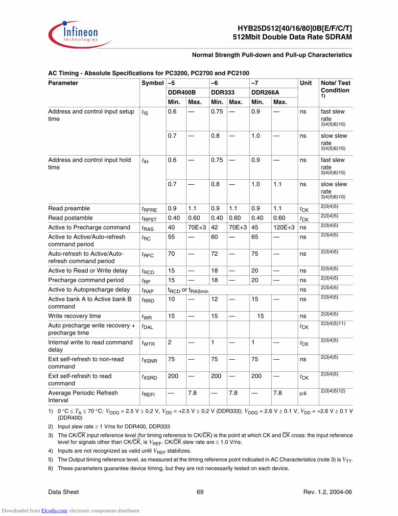
Data Sheet 69 Rev. 1.2, 2004-06
HYB25D512[40/16/80]0B[E/F/C/T]512Mbit Double Data Rate SDRAM
Normal Strength Pull-down and Pull-up Characteristics
Address and control input setup time
tIS 0.6 — 0.75 — 0.9 — ns fast slew rate3)4)5)6)10)
0.7 — 0.8 — 1.0 — ns slow slew rate3)4)5)6)10)
Address and control input hold time
tIH 0.6 — 0.75 — 0.9 — ns fast slew rate3)4)5)6)10)
0.7 — 0.8 — 1.0 1.1 ns slow slew rate3)4)5)6)10)
Read preamble tRPRE 0.9 1.1 0.9 1.1 0.9 1.1 tCK2)3)4)5)
Read postamble tRPST 0.40 0.60 0.40 0.60 0.40 0.60 tCK2)3)4)5)
Active to Precharge command tRAS 40 70E+3 42 70E+3 45 120E+3 ns 2)3)4)5)
Active to Active/Auto-refresh command period
tRC 55 — 60 — 65 — ns 2)3)4)5)
Auto-refresh to Active/Auto-refresh command period
tRFC 70 — 72 — 75 — ns 2)3)4)5)
Active to Read or Write delay tRCD 15 — 18 — 20 — ns 2)3)4)5)
Precharge command period tRP 15 — 18 — 20 — ns 2)3)4)5)
Active to Autoprecharge delay tRAP tRCD or tRASmin ns 2)3)4)5)
Active bank A to Active bank B command
tRRD 10 — 12 — 15 — ns 2)3)4)5)
Write recovery time tWR 15 — 15 — 15 ns 2)3)4)5)
Auto precharge write recovery + precharge time
tDAL tCK2)3)4)5)11)
Internal write to read command delay
tWTR 2 — 1 — 1 — tCK2)3)4)5)
Exit self-refresh to non-read command
tXSNR 75 — 75 — 75 — ns 2)3)4)5)
Exit self-refresh to read command
tXSRD 200 — 200 — 200 — tCK2)3)4)5)
Average Periodic Refresh Interval
tREFI — 7.8 — 7.8 — 7.8 µs 2)3)4)5)12)
1) 0 °C ≤ TA ≤ 70 °C; VDDQ = 2.5 V ± 0.2 V, VDD = +2.5 V ± 0.2 V (DDR333); VDDQ = 2.6 V ± 0.1 V, VDD = +2.6 V ± 0.1 V(DDR400)
2) Input slew rate ≥ 1 V/ns for DDR400, DDR333
3) The CK/CK input reference level (for timing reference to CK/CK) is the point at which CK and CK cross: the input referencelevel for signals other than CK/CK, is VREF. CK/CK slew rate are ≥ 1.0 V/ns.
4) Inputs are not recognized as valid until VREF stabilizes.
5) The Output timing reference level, as measured at the timing reference point indicated in AC Characteristics (note 3) is VTT.
6) These parameters guarantee device timing, but they are not necessarily tested on each device.
AC Timing - Absolute Specifications for PC3200, PC2700 and PC2100
Parameter Symbol –5 –6 –7 Unit Note/ TestCondition 1)DDR400B DDR333 DDR266A
Min. Max. Min. Max. Min. Max.
Downloaded from Elcodis.com electronic components distributor

Data Sheet 70 Rev. 1.2, 2004-06
HYB25D512[40/16/80]0B[E/F/C/T]512Mbit Double Data Rate SDRAM
Normal Strength Pull-down and Pull-up Characteristics
7) tHZ and tLZ transitions occur in the same access time windows as valid data transitions. These parameters are not referredto a specific voltage level, but specify when the device is no longer driving (HZ), or begins driving (LZ).
8) The specific requirement is that DQS be valid (HIGH, LOW, or some point on a valid transition) on or before this CK edge.A valid transition is defined as monotonic and meeting the input slew rate specifications of the device. When no writes werepreviously in progress on the bus, DQS will be transitioning from Hi-Z to logic LOW. If a previous write was in progress,DQS could be HIGH, LOW, or transitioning from HIGH to LOW at this time, depending on tDQSS.
9) The maximum limit for this parameter is not a device limit. The device operates with a greater value for this parameter, butsystem performance (bus turnaround) degrades accordingly.
10) Fast slew rate ≥ 1.0 V/ns , slow slew rate ≥ 0.5 V/ns and < 1 V/ns for command/address and CK & CK slew rate > 1.0 V/ns, measured between VIH(ac) and VIL(ac).
11) For each of the terms, if not already an integer, round to the next highest integer. tCK is equal to the actual system clockcycle time.
12) A maximum of eight Autorefresh commands can be posted to any given DDR SDRAM device.
Table 19 IDD Conditions
Parameter Symbol
Operating Current: one bank; active/ precharge; tRC = tRCMIN; tCK = tCKMIN;DQ, DM, and DQS inputs changing once per clock cycle; address and control inputs changing once every two clock cycles.
IDD0
Operating Current: one bank; active/read/precharge; Burst = 4;Refer to the following page for detailed test conditions.
IDD1
Precharge Power-Down Standby Current: all banks idle; power-down mode; CKE ≤ VILMAX; tCK = tCKMIN
IDD2P
Precharge Floating Standby Current: CS ≥ VIHMIN, all banks idle;CKE ≥ VIHMIN; tCK = tCKMIN, address and other control inputs changing once per clock cycle, VIN = VREF for DQ, DQS and DM.
IDD2F
Precharge Quiet Standby Current:CS ≥ VIHMIN, all banks idle; CKE ≥ VIHMIN; tCK = tCKMIN, address and other control inputs stableat ≥ VIHMIN or ≤ VILMAX; VIN = VREF for DQ, DQS and DM.
IDD2Q
Active Power-Down Standby Current: one bank active; power-down mode;CKE ≤ VILMAX; tCK = tCKMIN; VIN = VREF for DQ, DQS and DM.
IDD3P
Active Standby Current: one bank active; CS ≥ VIHMIN; CKE ≥ VIHMIN; tRC = tRASMAX; tCK = tCKMIN; DQ, DM and DQS inputs changing twice per clock cycle; address and control inputs changing once per clock cycle.
IDD3N
Operating Current: one bank active; Burst = 2; reads; continuous burst; address and control inputs changing once per clock cycle; 50% of data outputs changing on every clock edge; CL = 2 for DDR200 and DDR266A, CL = 3 for DDR333; tCK = tCKMIN; IOUT = 0 mA
IDD4R
Operating Current: one bank active; Burst = 2; writes; continuous burst; address and control inputs changing once per clock cycle; 50% of data outputs changing on every clock edge; CL = 2 for DDR200 and DDR266A, CL = 3 for DDR333; tCK = tCKMIN
IDD4W
Auto-Refresh Current: tRC = tRFCMIN, burst refresh IDD5
Self-Refresh Current: CKE ≤ 0.2 V; external clock on; tCK = tCKMIN IDD6
Operating Current: four bank; four bank interleaving with BL = 4; Refer to the following page for detailed test conditions.
IDD7
Downloaded from Elcodis.com electronic components distributor

Data Sheet 71 Rev. 1.2, 2004-06
HYB25D512[40/16/80]0B[E/F/C/T]512Mbit Double Data Rate SDRAM
Normal Strength Pull-down and Pull-up Characteristics
Table 20 IDD Specification
–7 –6 –5 Unit Note/Test Condition1)
1) Test conditions for typical values: VDD = 2.5 V (DDR266, DDR333), VDD = 2.6 V (DDR400), TA = 25 °C, test conditions formaximum values: VDD = 2.7 V, TA = 10 °C
DDR266A DDR333 DDR400B
Symbol Typ. Max. Typ. Max. Typ. Max.
IDD0 65 78 75 90 80 100 mA ×4/×8 2)3)
2) IDD specifications are tested after the device is properly initialized and measured at 133 MHz for DDR266, 166 MHz forDDR333, and 200 MHz for DDR400.
3) Input slew rate = 1 V/ns.
80 95 90 110 100 120 mA ×16 3)
IDD1 75 90 85 100 90 110 mA ×4/×8 3)
90 110 105 125 115 140 mA ×16 3)
IDD2P 1.5 4 1.6 4 1.7 4 mA 3)
IDD2F 20 24 25 30 30 36 mA 3)
IDD2Q 15 21 17 24 19 26 mA 3)
IDD3P 9 13 11 15 12 16 mA 3)
IDD3N 29 35 35 41 39 47 mA ×4/×8 3)
31 37 37 44 42 50 mA ×16 3)
IDD4R 67 78 77 90 85 100 mA ×4/×8 3)
85 100 105 125 120 145 mA ×16 3)
IDD4W 71 83 81 95 90 105 mA ×4/×8 3)
90 105 110 130 125 150 mA ×16 3)
IDD5 170 205 185 220 205 245 mA 3)4)
4) Enables on-chip refresh and address counters.
IDD6 2.6 5.1 2.7 5.2 2.8 5.2 mA 3)
IDD7 204 243 234 279 260 310 mA ×4/×8 3)
215 255 255 310 285 340 mA ×16 3)
Downloaded from Elcodis.com electronic components distributor

Data Sheet 72 Rev. 1.2, 2004-06
HYB25D512[40/16/80]0B[E/F/C/T]512Mbit Double Data Rate SDRAM
Normal Strength Pull-down and Pull-up Characteristics
5.2.1 IDD Current Measurement Conditions
IDD1: Operating Current: One Bank Operation
1. Only one bank is accessed with tRCMIN. Burst Mode, Address and Control inputs on NOP edge are changingonce per clock cycle. IOUT = 0 mA.
2. Timing patterns a) DDR266A (133 MHz, CL = 2): tCK = 7.5 ns, CL = 2, BL = 4, tRCD = 3 × tCK, tRC = 9 × tCK, tRAS = 5 × tCK
Setup: A0 N N R0 N P0 N N NRead: A0 N N R0 N P0 N NN - repeat the same timing with random address changing50% of data changing at every burst
b) DDR333 (166 MHz, CL = 2.5): tCK = 6 ns, CL = 2.5, BL = 4, tRCD = 3 × tCK, tRC = 9 × tCK, tRAS = 5 × tCKSetup: A0 N N R0 N P0 N N NRead: A0 N N R0 N P0 N N N - repeat the same timing with random address changing50% of data changing at every burst
c) DDR400 (200 MHz, CL = 3): tCK = 5 ns, BL = 4, tRCD = 3 × tCK, tRC = 11 × tCK, tRAS = 8 × tCKSetup: A0 N N R0 N N N N P0 N NRead: A0 N N R0 N N N N P0 N N - repeat the same timing with random address changing50% of data changing at every burst
3. Legend: A = Activate, R = Read, W = Write, P = Precharge, N = NOP
IDD7: Operating Current: Four Bank Operation
1. Four banks are being interleaved with tRCMIN. Burst Mode, Address and Control inputs on NOP edge are notchanging. IOUT = 0 mA.
2. Timing patternsa) DDR266A (133 MHz, CL = 2): tCK = 7.5 ns, CL = 2, BL = 4, tRRD = 2 × tCK, tRCD = 3 × tCK
Setup: A0 N A1 R0 A2 R1 A3 R2 N R3Read: A0 N A1 R0 A2 R1 A3 R2 N R3 - repeat the same timing with random address changing50% of data changing at every burst
b) DDR333 (166 MHz, CL = 2.5): tCK = 6 ns, CL = 2.5, BL = 4, tRRD = 2 × tCK, tRCD = 3 × tCKSetup: A0 N A1 R0 A2 R1 A3 R2 N R3Read: A0 N A1 R0 A2 R1 A3 R2 N R3 - repeat the same timing with random address changing50% of data changing at every burst
c) DDR400 (200 MHz, CL = 3): tCK = 5 ns, BL = 4, tRCD = 3 × tCK, tRC = 11 × tCK, tRAS = 8 × tCKSetup: A0 N N R0 N N N N P0 N NRead: A0 N N R0 N N N N P0 N N - repeat the same timing with random address changing50% of data changing at every burst
3. Legend: A = Activate, R = Read, W = Write, P = Precharge, N = NOP
Downloaded from Elcodis.com electronic components distributor

Data Sheet 73 Rev. 1.2, 2004-06
HYB25D512[40/16/80]0B[E/F/C/T]512Mbit Double Data Rate SDRAM
Timing Diagrams
6 Timing Diagrams
Figure 39 Data Input (Write), Timing Burst Length = 4
Figure 40 Data Output (Read), Timing Burst Length = 4
tDH
tDS
tDH
tDS
tDQSL
DI n = Data In for column n.3 subsequent elements of data in are applied in programmed order following DI n.
DI n
DQS
DQ
DM
Don’t Care
tDQSH
tQH (Data output hold time from DQS)
tDQSQ and tQH are only shown once and are shown referenced to different edges of DQS, only for clarify of illustration..
DQS
DQ
tDQSQ max
tQH
tDQSQ and tQH both apply to each of the four relevant edges of DQS.
tDQSQ max. is used to determine the worst case setup time for controller data capture.tQH is used to determine the worst case hold time for controller data capture.
Downloaded from Elcodis.com electronic components distributor

Data Sheet 74 Rev. 1.2, 2004-06
HYB25D512[40/16/80]0B[E/F/C/T]512Mbit Double Data Rate SDRAM
Timing Diagrams
Figure 41 Initialize and Mode Register Sets
t IH
200µ
s
t IS
t IH
t IS
t IH
t IS
t IH
t IS
t IH
t IS
t IH
t IS
t IH
t IS
t MR
Dt R
FC
t RF
Ct R
Pt M
RD
t MR
Dt C
L
t CK
t CH
t VT
D
PR
EE
MR
SM
RS
PR
EA
RA
RM
RS
NO
PA
CT
CO
DE
CO
DE
CO
DE
RA
CO
DE
CO
DE
CO
DE
RA
BA
0=L
BA
0=L
BA
Hig
h-Z
Hig
h-Z
Pow
er-u
p:V
DD
and
CK
stab
le
Ext
ende
d M
ode
Reg
iste
r S
etLo
ad M
ode
Reg
iste
r, R
eset
DLL
Load
Mod
eR
egis
ter
(with
A8
= L
)
VD
D
VD
DQ
VT
T (
Sys
tem
*)
VR
EF
CK
CK
E
Com
man
d
DM
A0-
A9,
A11
A10
BA
0, B
A1
DQ
S
DQ
LVC
MO
S L
OW
LE
VE
L
ALL
BA
NK
S
BA
0=H
BA
1=L
BA
1=L
BA
1=L
ALL
BA
NK
S
* V
TT
is n
ot a
pplie
d di
rect
ly to
the
devi
ce, h
owev
er t V
TD m
ust b
e
** t M
RD is
req
uire
d be
fore
any
com
man
d ca
n be
app
lied
and
The
two
Aut
oref
resh
com
man
ds m
ay b
e m
oved
to fo
llow
the
first
MR
S,
grea
ter
than
or
equa
l to
zero
to a
void
dev
ice
latc
hup.
200
cycl
es o
f CK
are
req
uire
d be
fore
a R
ead
com
man
d ca
n be
app
lied.
but p
rece
de th
e se
cond
Pre
char
ge A
ll co
mm
and.
Don
’t C
are
200
cycl
es o
f CK
**
CK
Downloaded from Elcodis.com electronic components distributor

Data Sheet 75 Rev. 1.2, 2004-06
HYB25D512[40/16/80]0B[E/F/C/T]512Mbit Double Data Rate SDRAM
Timing Diagrams
Figure 42 Power Down Mode
t IHt IS
t IHt IS
t ISt IS
t IHt IS
t CL
t CH
t CK
NO
PV
ALI
DV
ALI
D*
VA
LID
VA
LID
Ent
er P
ower
Dow
n M
ode
Exi
t Pow
erD
own
Mod
e
No
colu
mn
acce
sses
are
allo
wed
to b
e in
pro
gres
s at
the
time
pow
er d
own
is e
nter
ed.
* =
If th
is c
omm
and
is a
Pre
char
ge (
or if
the
devi
ce is
alre
ady
in th
e id
le s
tate
) th
en th
e po
wer
dow
n m
ode
show
n is
Pre
char
ge p
ower
dow
n. If
this
com
man
d is
an
Act
ive
(or
if at
leas
t one
row
is a
lread
y ac
tive)
, the
nth
e po
wer
dow
n m
ode
show
n is
Act
ive
pow
er d
own.
CK
E
Com
man
d
AD
DR
DQ
S
DQ
DM
Don
’t C
are
C K
C K
NO
P
Downloaded from Elcodis.com electronic components distributor
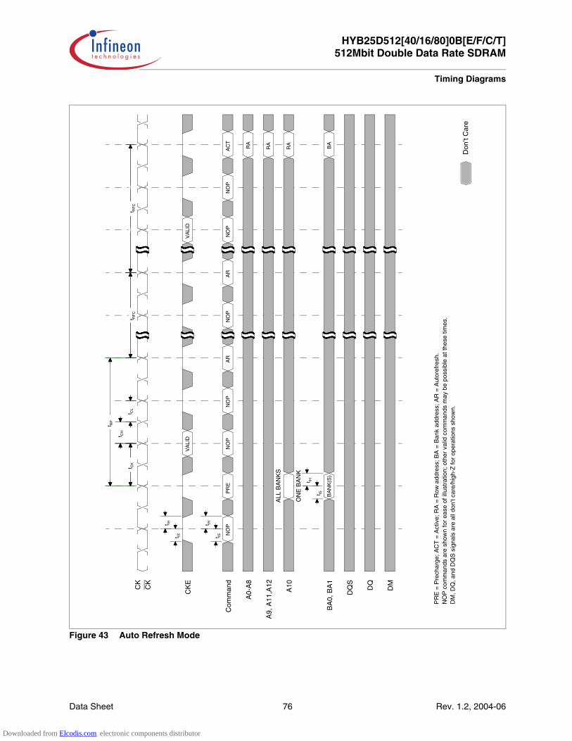
Data Sheet 76 Rev. 1.2, 2004-06
HYB25D512[40/16/80]0B[E/F/C/T]512Mbit Double Data Rate SDRAM
Timing Diagrams
Figure 43 Auto Refresh Mode
t IH
t IS
t IH
t IS
t IH
t IS
t RF
C
t RP
t CL
t CH
t CK
PR
EN
OP
NO
PA
RN
OP
AR
NO
PN
OP
NO
P
RA
RA
BA
PR
E =
Pre
char
ge; A
CT
= A
ctiv
e; R
A =
Row
add
ress
; BA
= B
ank
addr
ess;
AR
= A
utor
efre
sh.
NO
P c
omm
ands
are
sho
wn
for
ease
of i
llust
ratio
n; o
ther
val
id c
omm
ands
may
be
poss
ible
at t
hese
tim
es.
DM
, DQ
, and
DQ
S s
igna
ls a
re a
ll do
n't c
are/
high
-Z fo
r op
erat
ions
sho
wn.
VA
LID
VA
LID
AC
T
RA
CK
E
Com
man
d
A0-
A8
A9,
A11
,A12
A10
BA
0, B
A1
DQ
S
DQ
DM
BA
NK
(S)
Don
’t C
are
ALL
BA
NK
S
ON
E B
AN
K
t RF
C
CK
CK
Downloaded from Elcodis.com electronic components distributor
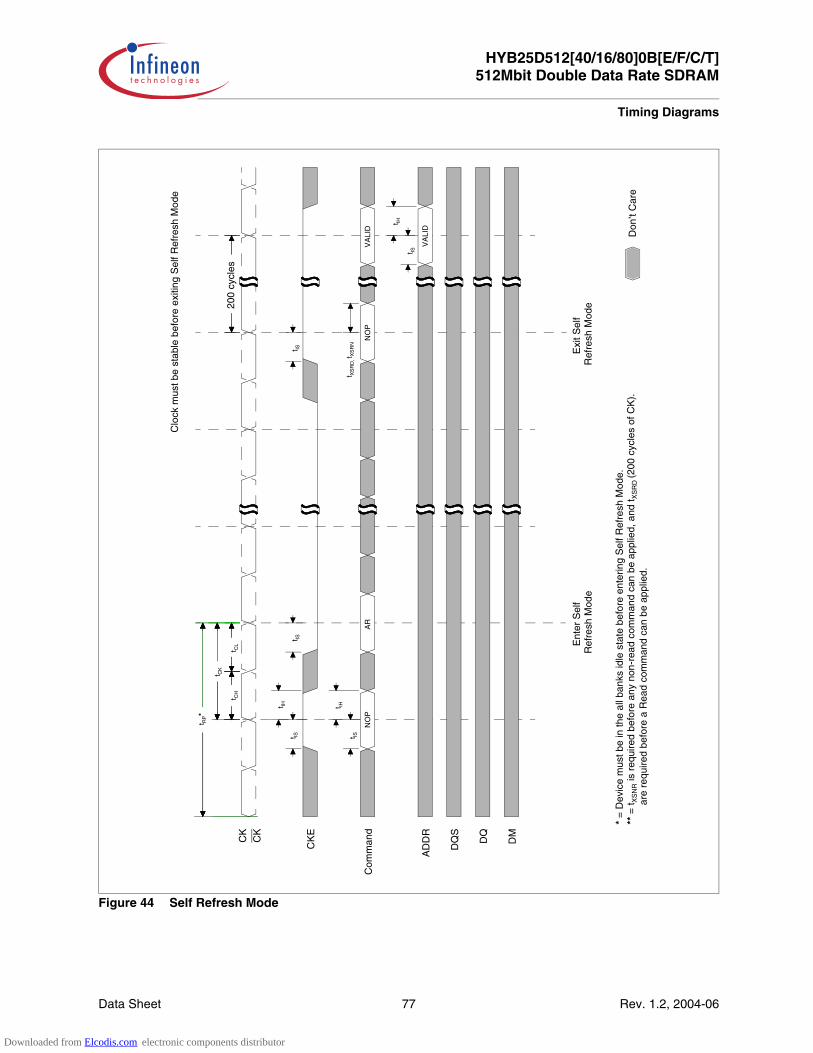
Data Sheet 77 Rev. 1.2, 2004-06
HYB25D512[40/16/80]0B[E/F/C/T]512Mbit Double Data Rate SDRAM
Timing Diagrams
Figure 44 Self Refresh Mode
200
cycl
es
t IH
t IS
t XS
RD
, tX
SR
N
t IH
t IS
t ISt IS
t IHt IS
t RP*
t CK
t CL
t CH
AR
VA
LID
NO
P
VA
LID
Ent
er S
elf
Ref
resh
Mod
eE
xit S
elf
Ref
resh
Mod
e
NO
P
* =
Dev
ice
mus
t be
in th
e al
l ban
ks id
le s
tate
bef
ore
ente
ring
Sel
f Ref
resh
Mod
e.**
= t X
SN
R is
req
uire
d be
fore
any
non
-rea
d co
mm
and
can
be a
pplie
d, a
nd t X
SR
D (2
00 c
ycle
s of
CK
).
CK
E
Com
man
d
AD
DR
DQ
S
DQ
DM
Don
’t C
are
are
req
uire
d be
fore
a R
ead
com
man
d ca
n be
app
lied.
CK
CK
Clo
ck m
ust b
e st
able
bef
ore
exiti
ng S
elf R
efre
sh M
ode
Downloaded from Elcodis.com electronic components distributor
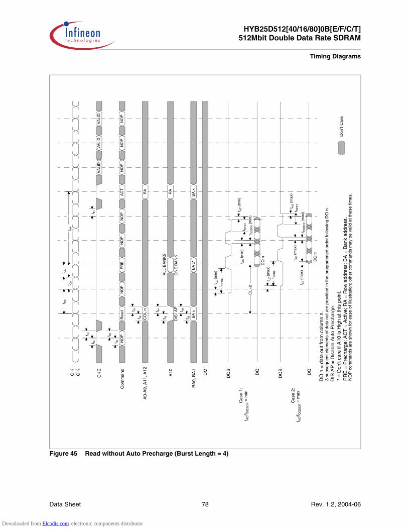
Data Sheet 78 Rev. 1.2, 2004-06
HYB25D512[40/16/80]0B[E/F/C/T]512Mbit Double Data Rate SDRAM
Timing Diagrams
Figure 45 Read without Auto Precharge (Burst Length = 4)
t HZ (
max
)
t LZ (
max
)
t HZ (
min
)t R
PS
T
t LZ (
min
)
t IHt IS
t IH
t IS
t IHt IS
t IH
t IS
t IH
t IHt IS
t RP
t CL
t CH
t CK
PR
EN
OP
NO
PA
CT
NO
PN
OP
NO
PN
OP
DO
n =
dat
a ou
t fro
m c
olum
n n.
3 su
bseq
uent
ele
men
ts o
f dat
a ou
t are
pro
vide
d in
the
prog
ram
med
ord
er fo
llow
ing
DO
n.
* =
Don
't ca
re if
A10
is H
igh
at th
is p
oint
.P
RE
= P
rech
arge
; AC
T =
Act
ive;
RA
= R
ow a
ddre
ss; B
A =
Ban
k ad
dres
s.N
OP
com
man
ds a
re s
how
n fo
r ea
se o
f illu
stra
tion;
oth
er c
omm
ands
may
be
valid
at t
hese
tim
es.
BA
xB
A x
VA
LID
VA
LID
VA
LID
NO
PR
ead
CO
L n
RA
RA
BA
x* D
O n
CK
E
Com
man
d
A10
BA
0, B
A1
DM
DQ
S
DQ
DQ
S
DQ
A0-
A9,
A11
, A12
ALL
BA
NK
S
ON
E B
AN
K
t DQ
SC
K (
max
)
t RP
RE
CL=
2t RP
RE
Don
’t C
are
Cas
e 1:
t AC/t D
QS
CK =
min
Cas
e 2:
t AC/t D
QS
CK =
max
t RP
ST
t AC (
max
)
t LZ (
max
)
t DQ
SC
K (
min
)
t AC (
min
)
DO
n
C K
C K
DIS
AP
DIS
AP
= D
isab
le A
uto
Pre
char
ge.
Downloaded from Elcodis.com electronic components distributor

Data Sheet 79 Rev. 1.2, 2004-06
HYB25D512[40/16/80]0B[E/F/C/T]512Mbit Double Data Rate SDRAM
Timing Diagrams
Figure 46 Read with Auto Pre charge (Burst Length = 4)
t HZ (
max
)
t LZ (
max
)
t HZ (
min
)t R
PS
T
t LZ (
min
)
t IHt IS
t IH
t IS
t IHt IS
t IH
t IS
t IH
t IHt IS
t RP
t CL
t CH
t CK
NO
PN
OP
NO
PA
CT
NO
PN
OP
NO
PN
OP
DO
n =
dat
a ou
t fro
m c
olum
n n.
3 su
bseq
uent
ele
men
ts o
f dat
a ou
t are
pro
vide
d in
the
prog
ram
med
ord
er fo
llow
ing
DO
n.
EN
AP
= e
nabl
e A
uto
Pre
char
ge.
AC
T =
act
ive;
RA
= r
ow a
ddre
ss.
NO
P c
omm
ands
are
sho
wn
for
ease
of i
llust
ratio
n; o
ther
com
man
ds m
ay b
e va
lid a
t the
se ti
mes
.
BA
x
VA
LID
VA
LID
VA
LID
NO
PR
ead
CO
L n
RA
RA
DO
n
CK
E
Com
man
d
A10
BA
0, B
A1
DM
DQ
S
DQ
DQ
S
DQ
A0-
A9,
A11
, A12
t DQ
SC
K (
max
)
t RP
RE
CL=
2t RP
RE
Don
’t C
are
Cas
e 1:
t AC/t D
QS
CK =
min
Cas
e 2:
t AC/t D
QS
CK =
max
t RP
ST
t AC (
max
)
t LZ (
max
)
t DQ
SC
K (
min
)
t AC (
min
)
DO
n
EN
AP
BA
x
C K
C K
t LZ (
min
)
Downloaded from Elcodis.com electronic components distributor

Data Sheet 80 Rev. 1.2, 2004-06
HYB25D512[40/16/80]0B[E/F/C/T]512Mbit Double Data Rate SDRAM
Timing Diagrams
Figure 47 Bank Read Access (Burst Length = 4)
t HZ (
max
)
t LZ (
max
)
t HZ (
min
)
t RP
ST
t LZ (
min
)
t IHt IS
t IH
t IS
t IHt IS
t IH
t IS
t IHt IS
t CL
t CH
t CK
Rea
dN
OP
PR
EN
OP
NO
PA
CT
NO
PN
OP
BA
xB
A x
*
VA
LID
NO
PA
CT
RA
RA
BA
x
DO
n
C K
C K
CK
E
Com
man
d
A10
BA
0, B
A1
DM
DQ
S
DQ
DQ
S
DQ
t DQ
SC
K (
max
)
t RP
RE
CL=
2C
L=2t R
PR
E
Don
’t C
are
Cas
e 1:
t AC/t D
QS
CK =
min
Cas
e 2:
t AC/t D
QS
CK =
max
t RP
ST
t AC (
max
)
t LZ (
max
)
t DQ
SC
K (
min
)
t AC (
min
)
DO
n
CO
L n
RA
RA
ALL
BA
NK
SR
A
ON
E B
AN
KD
IS A
P
BA
x
t RP
DO
n =
dat
a ou
t fro
m c
olum
n n.
3 su
bseq
uent
ele
men
ts o
f dat
a ou
t are
pro
vide
d in
the
prog
ram
med
ord
er fo
llow
ing
DO
n.
DIS
AP
= d
isab
le A
uto
Pre
char
ge.
* =
Don
't ca
re if
A10
is H
igh
at th
is p
oint
.P
RE
= P
rech
arge
; AC
T =
Act
ive;
RA
= R
ow a
ddre
ss; B
A =
Ban
k ad
dres
s.N
OP
com
man
ds a
re s
how
n fo
r ea
se o
f illu
stra
tion;
oth
er c
omm
ands
may
be
valid
at t
hese
tim
es.
t RC
D
A0-
A9,
A11
, A12
t RA
S
t RC
t LZ (
min
)
Downloaded from Elcodis.com electronic components distributor
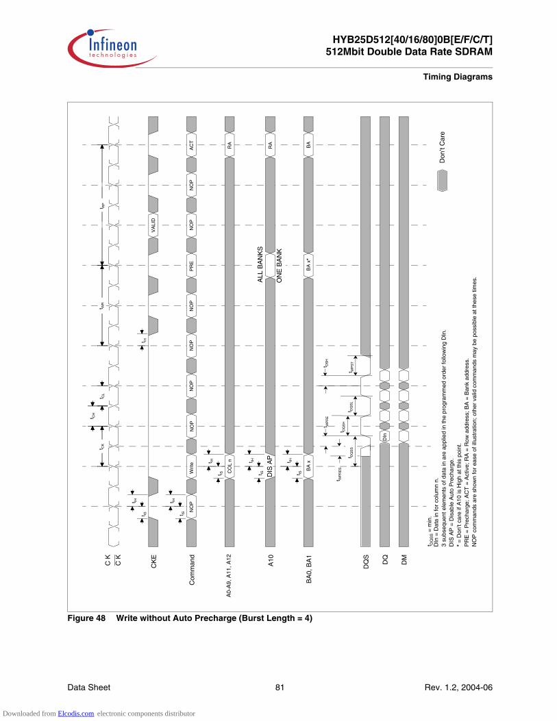
Data Sheet 81 Rev. 1.2, 2004-06
HYB25D512[40/16/80]0B[E/F/C/T]512Mbit Double Data Rate SDRAM
Timing Diagrams
Figure 48 Write without Auto Precharge (Burst Length = 4)
t IH
t WP
ST
t DQ
SL
t IH
t IS
t IH
t IS
t IH
t IS
t IH
t IS
t IHt IS
t RP
t CL
t CH
t CK
NO
PN
OP
NO
PP
RE
NO
PN
OP
AC
TN
OP
BA
xB
A
NO
PW
rite
CO
L n
RA
RA
BA
x*
VA
LID
DIn
= D
ata
in fo
r co
lum
n n.
3 su
bseq
uent
ele
men
ts o
f dat
a in
are
app
lied
in th
e pr
ogra
mm
ed o
rder
follo
win
g D
In.
DIS
AP
= D
isab
le A
uto
Pre
char
ge.
* =
Don
't ca
re if
A10
is H
igh
at th
is p
oint
.P
RE
= P
rech
arge
; AC
T =
Act
ive;
RA
= R
ow a
ddre
ss; B
A =
Ban
k ad
dres
s.N
OP
com
man
ds a
re s
how
n fo
r ea
se o
f illu
stra
tion;
oth
er v
alid
com
man
ds m
ay b
e po
ssib
le a
t the
se ti
mes
.
DIn
C K
C K
CK
E
Com
man
d
A10
BA
0, B
A1
DQ
S
DQ
DM
DIS
AP
ALL
BA
NK
S
ON
E B
AN
K
t WR
t WP
RE
St D
QS
H
Don
’t C
are
A0-
A9,
A11
, A12
t DQ
SS =
min
.
t DQ
SS
t WP
RE
t DS
H
Downloaded from Elcodis.com electronic components distributor

Data Sheet 82 Rev. 1.2, 2004-06
HYB25D512[40/16/80]0B[E/F/C/T]512Mbit Double Data Rate SDRAM
Timing Diagrams
Figure 49 Write with Auto Pre charge (Burst Length = 4)
NO
P c
omm
ands
are
sho
wn
for
ease
of i
llust
ratio
n; o
ther
val
id c
omm
ands
may
be
poss
ible
at t
hese
tim
es.
AC
T =
Act
ive;
RA
= R
ow a
ddre
ss; B
A =
Ban
k ad
dres
s.
t IH
t WP
ST
t DQ
SL
t IH
t IS
t IH
t IS
t IH
t IS
t IH
t ISt IS
t RP
t CL
t CH
t CK
NO
PN
OP
NO
PN
OP
NO
PN
OP
AC
TN
OP
BA
xB
A
NO
PW
rite
CO
L n
RA
RA
VA
LID
DIn
= D
ata
in fo
r co
lum
n n.
3 su
bseq
uent
ele
men
ts o
f dat
a in
are
app
lied
in th
e pr
ogra
mm
ed o
rder
follo
win
g D
In.
EN
AP
= E
nabl
e A
uto
Pre
char
ge.
C K
C K
CK
E
Com
man
d
A10
BA
0, B
A1
DQ
S
DQ
DM
t WR
t DQ
SS
t WP
RE
S
t DQ
SH
Don
’t C
are
VA
LID
VA
LID
EN
AP
A0-
A9,
A11
, A12
t DA
L
t DQ
SS =
min
.
t DS
H
t WP
RE
DIn
Downloaded from Elcodis.com electronic components distributor

Data Sheet 83 Rev. 1.2, 2004-06
HYB25D512[40/16/80]0B[E/F/C/T]512Mbit Double Data Rate SDRAM
Timing Diagrams
Figure 50 Bank Write Access (Burst Length = 4)
t WP
ST
t DQ
SL
t IH
t IS
t IH
t IS
t IH
t IS
t IH
t IS
t IH
t IS
t CL
t CH
t CK
t RA
S
Writ
eN
OP
NO
PN
OP
NO
PP
RE
NO
PN
OP
BA
x
NO
PA
CT
RA
RA
DI n
= d
ata
in fo
r co
lum
n n.
3 su
bseq
uent
ele
men
ts o
f dat
a in
are
app
lied
in th
e pr
ogra
mm
ed o
rder
follo
win
g D
I n.
DIS
AP
= D
isab
le A
uto
Pre
char
ge.
* =
don
't ca
re if
A10
is H
igh
at th
is p
oint
.P
RE
= P
rech
arge
; AC
T =
Act
ive;
RA
= R
ow a
ddre
ss.
NO
P c
omm
ands
are
sho
wn
for
ease
of i
llust
ratio
n; o
ther
val
id c
omm
ands
may
be
poss
ible
at t
hese
tim
es.
DIn
VA
LID
BA
x
CK
E
Com
man
d
A10
BA
0, B
A1
DQ
S
DQ
DMCK
CK
t WP
RE
St W
R
t RC
D
ALL
BA
NK
S
ON
E B
AN
KD
IS A
P
Don
’t C
are
A0-
A9,
A11
, A12
Col
n
BA
x
t DQ
SS
t DQ
SH
t DS
H
t WP
RE
t DQ
SS =
min
.
Downloaded from Elcodis.com electronic components distributor

Data Sheet 84 Rev. 1.2, 2004-06
HYB25D512[40/16/80]0B[E/F/C/T]512Mbit Double Data Rate SDRAM
Timing Diagrams
Figure 51 Write DM Operation (Burst Length = 4)
t IH
t WP
ST
t DQ
SL
t IH
t IS
t IH
t ISt IS
t RP
t CL
t CH
t CK
NO
PN
OP
NO
PP
RE
NO
PN
OP
AC
TN
OP
NO
PW
rite
CO
L n
RA
DIn
CK
CK
CK
E
Com
man
d
A10
BA
0, B
A1
DQ
S
DQ
DM
t WR
t DQ
SS
Don
’t C
are
VA
LID
t IH
t IS
t IH
t IS
BA
xB
A
RA
BA
x*
ALL
BA
NK
S
ON
E B
AN
KD
IS A
P
DI n
= d
ata
in fo
r co
lum
n n.
3 su
bseq
uent
ele
men
ts o
f dat
a in
are
app
lied
in th
e pr
ogra
mm
ed o
rder
follo
win
g D
I n (
the
seco
nd e
lem
ent o
f the
4 is
mas
ked)
.D
IS A
P =
Dis
able
Aut
o P
rech
arge
.*
= D
on't
care
if A
10 is
Hig
h at
this
poi
nt.
PR
E =
Pre
char
ge; A
CT
= A
ctiv
e; R
A =
Row
add
ress
; BA
= B
ank
addr
ess.
NO
P c
omm
ands
are
sho
wn
for
ease
of i
llust
ratio
n; o
ther
val
id c
omm
ands
may
be
poss
ible
at t
hese
tim
es.
A0-
A9,
A11
, A12
t DQ
SH
t DS
H
t DQ
SS =
min
.
t WP
RE
S
Downloaded from Elcodis.com electronic components distributor

HYB25D512[40/16/80]0B[E/F/C/T]512Mbit Double Data Rate SDRAM
System Characteristics for DDR SDRAMs
Data Sheet 85 Rev. 1.2, 2004-06 08122003-RMYD-6BJP
7 System Characteristics for DDR SDRAMsThe following specification parameters are required in systems using DDR400, DDR333 & DDR266 devices toensure proper system performance. These characteristics are for system simulation purposes and are guaranteedby design.
Table 21 Input Slew Rate for DQ, DQS, and DM
AC Characteristics Symbol DDR400 DDR333 DDR266 Units Notes
Parameter Min. Max. Min. Max. Min. Max.
DM/DQS inout slew rate measured berween VIH(DC), VIL (DC), and VIL(DC), VIH (DC)
DCSLEW 0.5 4.0 0.5 4.0 0.5 4.0 V/ns 1)2)
1) Pullup slew rate is characterized under the test conditions as shown in Figure 52.
2) DQS, DM, amd DQ input slew rate is specified to prevent doble clocking of data and preserve setup and hold times. Signaltransitions through the DC region must be monotonic.
Table 22 Input Setup & Hold Time Derating for Slew Rate
Input Slew Rate ∆tIS tIH Units Notes
0.5 V/ns 0 0 ps 1)
1) A derating factor will be used to increase tIS and tIH in the case where the input slew rate is below 0.5 V/ns asshown in Table 22. The input slew rate is based on the lesser of the slew rates determined by either VIH (AC) toVIL (AC) or VIH (DC) to VIL (DC), similarly for rising transitions. Aderating factor applies to speed bins DDR200,DDR266, and DDR333.
0.4 V/ns +50 0 ps
0.3 V/ns +100 0 ps
Table 23 Input/Output Setup and Hold TIme Derating for Slew Rate
I/O Input Slew Rate ∆tDS tDH Units Notes
0.5 ns/V 0 0 ps 1)
1) Table 23 is used to increase tDS and tDH in the case where the I/O slew rate is below 0.5 V/ns. The I/O slewrate is based on the lesser of the AV – AC slew rate and the DC – DC slew rate. The input slew rate is basedon the lesser of the slew rates determined by either VIH (AC) to VIL (AC) or VIH (DC) to VIL (DC), and similarly for risingtransitions. A derating factor applies to speed bins DDR200, DDR266 and DDR333.
0.4 ns/V +75 +75 ps
0.3 ns/V +100 +100 ps
Table 24 Input/Output Setup and Hold Derating for Rise/Fall Delta Slew Rate
Delta Slew Rate ∆tDS tDH Units Notes
±0.0 ns/V 0 0 ps 1)
1) A derating factor will be used to increase tDS and tDH in the case where DQ, DM and DQS slew rates differ, as shown inTables 15 & 16. Input slew rate is based on the larger of AC – AC delta rise, fall rate and DC – DC delta rise, fall rate. Inputslew rate is based on the lesser of the slew rates determined by either VIH (AC) to VIL (AC) or VIH (DC) to VIL (DC), similarly forrising transitions.The delta rise/fall rate is calculated as:1/(Slew Rate1) – 1/(Slew Rate2)For example: If Slew Rate 1 is 0.5 V/ns and Slew Rate 2 is 0.4 V/ns, then the delta rise, fall rate is –0.5 ns/V. Using thetable given, this would result in the need for an increase in tDS and tDH of 100 ps. A derating factor applies to speed binsDDR200, DDR266, and DDR333.
±0.25 ns/V +50 +50 ps
±0.5 ns/V +100 +100 ps
Downloaded from Elcodis.com electronic components distributor

HYB25D512[40/16/80]0B[E/F/C/T]512Mbit Double Data Rate SDRAM
System Characteristics for DDR SDRAMs
Data Sheet 86 Rev. 1.2, 2004-06 08122003-RMYD-6BJP
Table 25 Output Slew Rate Characteristrics (×4, ×8 Devices only)
Slew Rate Characteristic Typical Range (V/ns) Minumum (V/ns) Maximum (V/ns) Notes
Pullup Slew Rate 1.2 – 2.5 1.0 4.5 1)2)3)4)5)6)
1) Pullup slew rate is characterized under the test conditions as shown in Figure 52
2) Pullup slew rate is measured between (VDDQ/2 – 320 mV ± 250 mV)Pulldown slew rate is measured between (VDDQ/2 + 320 mV ± 250 mV)Pullup and Pulldown slew rate conditions are to be met for any pattern of data, including all outputs switching and only oneoutput switching.Example: For typical slew rate, DQ0 is switchingFor minimum slew rate, all DQ bits are switchiung worst case patternFor maximum slew rate, only one DQ is switching from either high to low, or low to high.the remainig DQ bits remain the same as previous state.
3) Evaluation conditionsTypical: 25 °C (T Ambient), VDDQ = nominal, typical processMinimum: 70 °C (T Ambient), VDDQ = minimum, slow – slow processMaximum: 0 °C (T Ambient), VDDQ = maximum, fast – fast process
4) Verified under typical conditions for qualification purposes.
5) TSOP II package devices only.
6) Only intended for operation up to 266 Mbps per pin.
Pulldown Slew Rate 1.2 – 2.5 1.0 4.5 2)3)4)5)5)7)2)2)
7) Pulldown slew rate is measured under the test conditions shown in Figure 53.
Table 26 Output Slew Rate Characteristics (×16 Devices only)
Slew Rate Characteristic Typical Range (V/ns) Minimum (V/ns) Maximum(V/ns) Notes
Pullup Slew Rate 1.2 – 2.5 0.7 5.0 1)2)3)4)5)6)
1) Pullup slew rate is characterizted under the test conditions as shown in Figure 52
2) Pullup slew rate is measured between (VDDQ/2 – 320 mV ± 250 mV)Pulldown slew rate is measured between (VDDQ/2 + 320 mV ± 250mV)Pullup and Pulldown slew rate conditions are to be met for any pattern of data, including all outputs switching and only oneoutput switching.Example: For typical slew rate, DQ0 is switchingFor minimum slew rate, all DQ bits are switchiung worst case patternFor maximum slew rate, only one DQ is switching from either high to low, or low to high.the remainig DQ bits remain the same as previous state.
3) Evaluation conditionsTypical: 25 °C (T Ambient), VDDQ = nominal, typical processMinimum: 70 °C (T Ambient), VDDQ = minimum, slow – slow processMaximum: 0 °C (T Ambient), VDDQ = maximum, fast – fast process
4) Verified under typical conditions for qualification purposes.
5) TSOP II package devices only.
6) Only intended for operation up to 266 Mbps per pin.
Pulldown Slew Rate 1.2 – 2.5 0.7 5.0 7)
7) Pulldown slew rate is measured under the test conditions shown in Figure 53.
Table 27 Output Slew Rate Matching Ratio Characteristics
Slew Rate Characteristic DDR266A DDR266B DDR200 Notes
Parameter Min. Max. Min. Max. Min. Max.
Output SLew Rate Matching Ratio (Pullup to Pulldown)
— — — — 0.71 1.4 1) 2)
Downloaded from Elcodis.com electronic components distributor

HYB25D512[40/16/80]0B[E/F/C/T]512Mbit Double Data Rate SDRAM
System Characteristics for DDR SDRAMs
Data Sheet 87 Rev. 1.2, 2004-06 08122003-RMYD-6BJP
Figure 52 Pullup slew rate test load
Figure 53 Pulldown slew rate test load
1) The ratio of pullup slew rate to pulldown slew rate is specified for the same temperature and voltage, over the entiretemperature and voltage range. For a given output, it represents the maximum difference between pullup and pulldowndrivers due to process variation.
2) DQS, DM, and DQ input slew rate is specified to prevent double clocking of data and preserve setup and hold times. Signaltransitions through the DC region must be monotonic
MPBD1990
Output50 Ω
Test point
VDDQ
MPBD2000
Output50 Ω
Test point
VSSQ
Downloaded from Elcodis.com electronic components distributor

Data Sheet 88 Rev. 1.2, 2004-06
HYB25D512[40/16/80]0B[E/F/C/T]512Mbit Double Data Rate SDRAM
Package Outlines
8 Package OutlinesThere are two package types used for this product family each in lead-free and lead-containing assembly:
• P-TFBGA: Plastic Thin Fine-Pitch Ball Grid Array Package
• P-TSOPII: Plastic Thin Small Outline Package Type II
Figure 54 Package Outline of P-TFBGA-60-[9/22] (green/non-green)
Table 28 TFBGA Common Package Properties (non-green/green)
Description Size Units
Ball Size 0.460 mm
Recommended Landing Pad 0.350 mm
Recommended Solder Mask 0.450 mm
GPA09554
2.2
MA
X.
1)
11 x 1 = 11
8 x
0.8
= 6
.4
3)
2)
1
1.2
MA
X.
0.31
MIN
.
60x±0.05ø0.46
SEATING PLANE
0.18 MAX.
12
A2)
B
0.8
10
0.2
ø0.15 MC A
Mø0.08B
0.1 CC0.1
C
4)5)
2) Middle of Packages Edges3) Package Orientation Mark A14) Bad Unit Marking (BUM)5) Die Sort Fiducial
1) Dummy Pads without Ball
Downloaded from Elcodis.com electronic components distributor

HYB25D512[40/16/80]0B[E/F/C/T]512Mbit Double Data Rate SDRAM
Package Outlines
Data Sheet 89 Rev. 1.2, 2004-06
Figure 55 Package Outline of P-TSOPII-66-1 (green/non-green)
GPX09261
0.65 Basic
0.35 +0.1-0.05
0.805 REF
0.05
MIN
.
1.20
MAX
.
22.22Lead 1
10.16
0.5
11.760.1
0.25
Bas
ic
Gage Plane
Seating Plane
±0.13
±0.2
±0.13
±0.1
Downloaded from Elcodis.com electronic components distributor

Published by Infineon Technologies AG
w w w . i n f i n e o n . c o m
Downloaded from Elcodis.com electronic components distributor