© copyright 2009 xilinx copyright 2011 xilinx may 2012 zynq-7000 epp introduction where arm...
TRANSCRIPT
© Copyright 2009 XilinxCopyright 2011 Xilinx
May 2012
Zynq-7000 EPP Introduction
Where ARM Processors Meet HW Programmability
Copyright 2011 Xilinx© Copyright 2009 XilinxCopyright 2011 XilinxCopyright 2011 XilinxPage 2
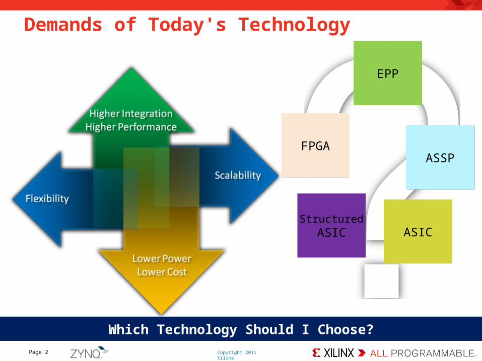
Demands of Today's Technology
Which Technology Should I Choose?
ASSPFPGA
StructuredASIC
EPP
ASIC

Copyright 2011 Xilinx© Copyright 2009 XilinxCopyright 2011 Xilinx
Current Selections Equal Compromise
Page 3
ASIC ASSP2 Chip
Solution
Performance + +
Power + + - Unit Cost + + -TCO + +Risk - + +TTM - + +Flexibility - - +Scalability - +
Conflicting Demands Not Served
+ positive, - negative, neutral

Copyright 2011 Xilinx© Copyright 2009 XilinxCopyright 2011 XilinxCopyright 2011 Xilinx
Breakthrough Processing Platform– Higher system performance, lower total power– Flexible and scalable solution
Industry Standard Design Environments– Well defined SW programming model– Familiar SW & HW design flows
Flexible Accelerators and IP– World class 28nm programmable logic architecture– Standard AMBA® 4 AXI interfaces
Broad Ecosystem Support– Tools, OS’s & IPs– Middleware, codecs– System integrators and training partners.
Page 4
Introducing the Zynq™-7000 EPP
Familiar Processing System + Scalable Programmable Logic
Copyright 2011 Xilinx© Copyright 2009 XilinxCopyright 2011 XilinxCopyright 2011 Xilinx
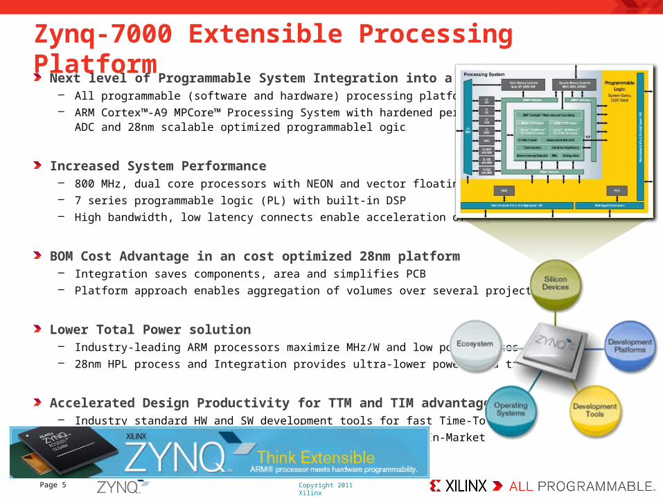
Next level of Programmable System Integration into a true SoC– All programmable (software and hardware) processing platform – ARM Cortex™-A9 MPCore™ Processing System with hardened peripherals,
ADC and 28nm scalable optimized programmablel ogic c
Increased System Performance– 800 MHz, dual core processors with NEON and vector floating point units– 7 series programmable logic (PL) with built-in DSP– High bandwidth, low latency connects enable acceleration of key functions
BOM Cost Advantage in an cost optimized 28nm platform– Integration saves components, area and simplifies PCB– Platform approach enables aggregation of volumes over several projects
Lower Total Power solution– Industry-leading ARM processors maximize MHz/W and low power states– 28nm HPL process and Integration provides ultra-lower power data transfers
Accelerated Design Productivity for TTM and TIM advantage– Industry standard HW and SW development tools for fast Time-To-Market– Flexible and scalable platform enables extended Time-In-Market– Extensive ecosystem of tools and solutions partners
Page 5
Zynq-7000 Extensible Processing Platform

Copyright 2011 Xilinx© Copyright 2009 XilinxCopyright 2011 XilinxCopyright 2011 Xilinx
Complete ARM®-based Processing System– Dual ARM Cortex™-A9 MPCore™, processor centric– Integrated memory controllers & peripherals– Fully autonomous to the programmable logic
Tightly Integrated Programmable Logic– Used to extend processing system– High performance AXI based Interface– Scalable density and performance
Flexible Array of I/O– Wide range of external multi-standard I/O– High performance integrated serial transceivers– Analog-to-Digital Converter inputs
Page 6
Zynq-7000 Family Highlights
Software & Hardware Programmable
7 SeriesProgrammable
Logic
Common Peripherals
CustomPeripherals
Common Accelerators
Custom Accelerators
CommonPeripherals
ProcessingSystem
MemoryInterfaces
ARM®
Dual Cortex-A9 MPCore™ System
Copyright 2011 Xilinx© Copyright 2009 XilinxCopyright 2011 XilinxCopyright 2011 XilinxPage 7
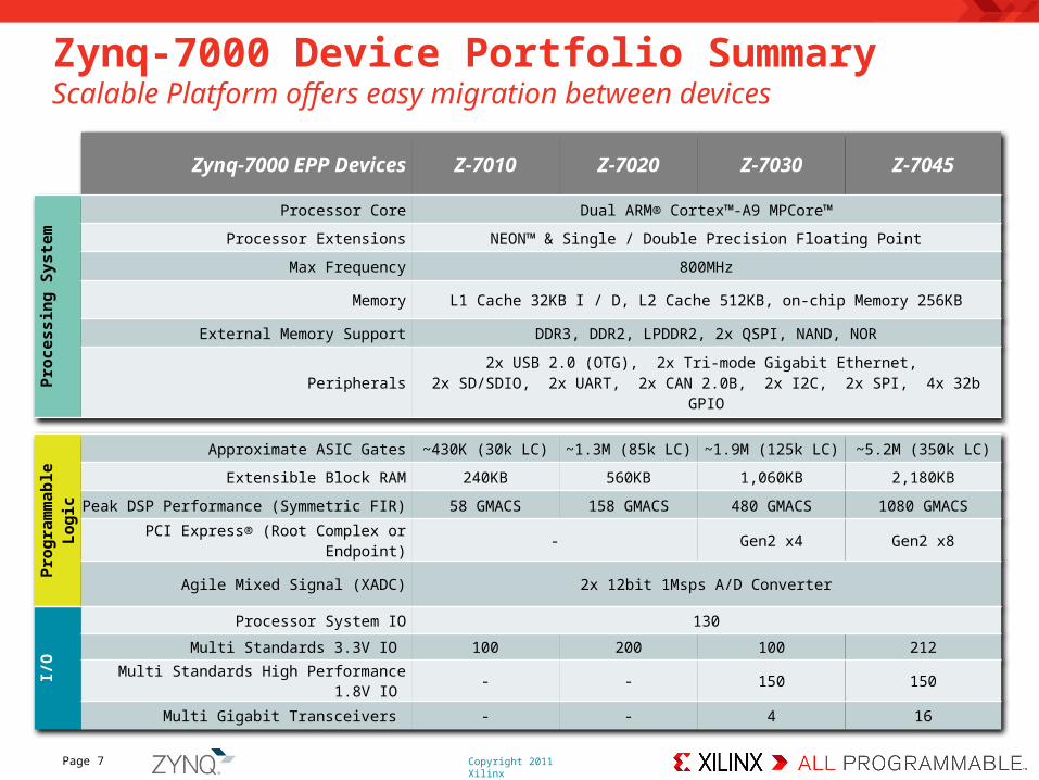
Zynq-7000 Device Portfolio SummaryScalable Platform offers easy migration between devices
Zynq-7000 EPP Devices Z-7010 Z-7020 Z-7030 Z-7045
Processing Syste
m
Processor Core Dual ARM® Cortex™-A9 MPCore™
Processor Extensions NEON™ & Single / Double Precision Floating Point
Max Frequency 800MHz
Memory L1 Cache 32KB I / D, L2 Cache 512KB, on-chip Memory 256KB
External Memory Support DDR3, DDR2, LPDDR2, 2x QSPI, NAND, NOR
Peripherals 2x USB 2.0 (OTG), 2x Tri-mode Gigabit Ethernet, 2x SD/SDIO, 2x UART, 2x CAN 2.0B, 2x I2C, 2x SPI, 4x 32b GPIO
Programmable
Logic
Approximate ASIC Gates ~430K (30k LC) ~1.3M (85k LC) ~1.9M (125k LC) ~5.2M (350k LC)
Extensible Block RAM 240KB 560KB 1,060KB 2,180KB
Peak DSP Performance (Symmetric FIR) 58 GMACS 158 GMACS 480 GMACS 1080 GMACS
PCI Express® (Root Complex or Endpoint) - Gen2 x4 Gen2 x8
Agile Mixed Signal (XADC) 2x 12bit 1Msps A/D Converter
I/O
Processor System IO 130
Multi Standards 3.3V IO 100 200 100 212
Multi Standards High Performance 1.8V IO - - 150 150
Multi Gigabit Transceivers - - 4 16
Copyright 2011 Xilinx© Copyright 2009 XilinxCopyright 2011 Xilinx
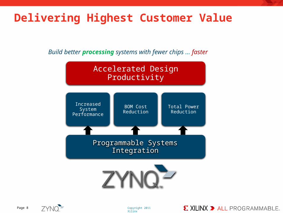
Build better systems fasterBuild better processing systems with fewer chips … faster
Increased System Performance
BOM Cost Reduction
Total Power Reduction
Accelerated Design Productivity
Delivering Highest Customer Value
Programmable Systems Integration
Page 8

Copyright 2011 Xilinx© Copyright 2009 XilinxCopyright 2011 XilinxCopyright 2011 Xilinx
Programmable Systems Integration
ALL Programmable Platform Integrating Multiple Components– Hardware and Software programmable– Board component reduction– Security & reliability– Manufacturing benefits
Defines Extensibility– Create custom, flexible ASSP– Co-processing offload by accelerating software functions
ARM Programmability + FPGA Flexibility in a Single Chip
Programmable Systems Integration
Increased System Performance
BOM Cost Reduction
Total Power Reduction
Accelerated Design Productivity
Page 9

Copyright 2011 Xilinx© Copyright 2009 XilinxCopyright 2011 XilinxCopyright 2011 Xilinx
Increased System Performance
Hardware Performance– Dual Core ARM Cortex A9’s with NEON and
vector floating point– High performance programmable logic– Tightly coupled processor and programmable logic
• High throughput / low latency
– Massive parallel DSP processing– High performance I/Os and transceivers (12.5Gbps)
Accelerating Processor Performance– Increasing software performance through co-processing
accelerators– Low latency interfacing for efficient co-processor
implementation
Optimized Balance of Performance and Power
Programmable Systems Integration
Increased System Performance
BOM Cost Reduction
Total Power Reduction
Accelerated Design Productivity
ElementsPerformance
(up to)
Processors (each) 800 MHz
Processors (aggregate) 4000 DMIPs
DSP (each) 600MHz
DSP (aggregate) 1080 GMACs
Transceivers (each) 12.5Gbps
Transceivers (aggregate) 200Gbps
SW Acceleration using PL >10x
Page 10

Copyright 2011 Xilinx© Copyright 2009 XilinxCopyright 2011 XilinxCopyright 2011 Xilinx
BOM Cost Reduction
Reduced Devices per Board– Processors, PLDs, DSPs– A/D converters– Power supplies, fans, etc…
Reduced PCB Complexity– Fewer traces/interconnect/layers– Fewer power supplies– Smaller overall PCB
In System Reconfiguration Combines Multiple Device Functions– HW can be configured and reconfigured only with the needed function at a given time
PS Aggregates Numerous IP Royalties for Net Cost Benefit– ASIC or full FPGA solutions would require purchase of these IPs from 3 rd parties.
Multi-chip Zynq-7000
PCB / Other Components
EPP
DSP
BO
M C
os
t
FPGA
Processor
Platform approach enables aggregation of volumes for lower price
Programmable Systems Integration
Increased System Performance
BOM Cost Reduction
Total Power Reduction
Accelerated Design Productivity
Up to 40% BOM Cost Reduction vs. Multi-Chip Solutions
Page 11
Copyright 2011 Xilinx© Copyright 2009 XilinxCopyright 2011 XilinxCopyright 2011 Xilinx
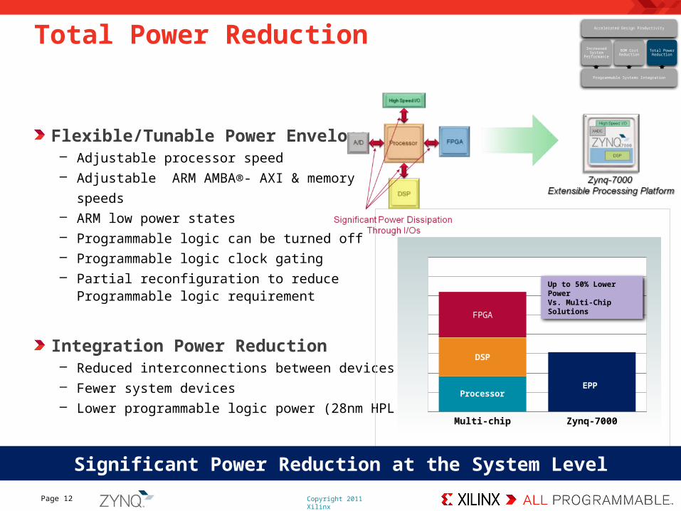
Total Power Reduction
Flexible/Tunable Power Envelope– Adjustable processor speed– Adjustable ARM AMBA®- AXI & memory
speeds– ARM low power states– Programmable logic can be turned off– Programmable logic clock gating– Partial reconfiguration to reduce
Programmable logic requirement
Integration Power Reduction– Reduced interconnections between devices– Fewer system devices– Lower programmable logic power (28nm HPL process)
Multi-chip Zynq-7000
DSP
FPGA
ProcessorEPP
Up to 50% Lower PowerVs. Multi-Chip Solutions
Significant Power Reduction at the System Level
Programmable Systems Integration
Increased System Performance
BOM Cost Reduction
Total Power Reduction
Accelerated Design Productivity
Page 12
Copyright 2011 Xilinx© Copyright 2009 XilinxCopyright 2011 XilinxCopyright 2011 Xilinx
Accelerated Design Productivity
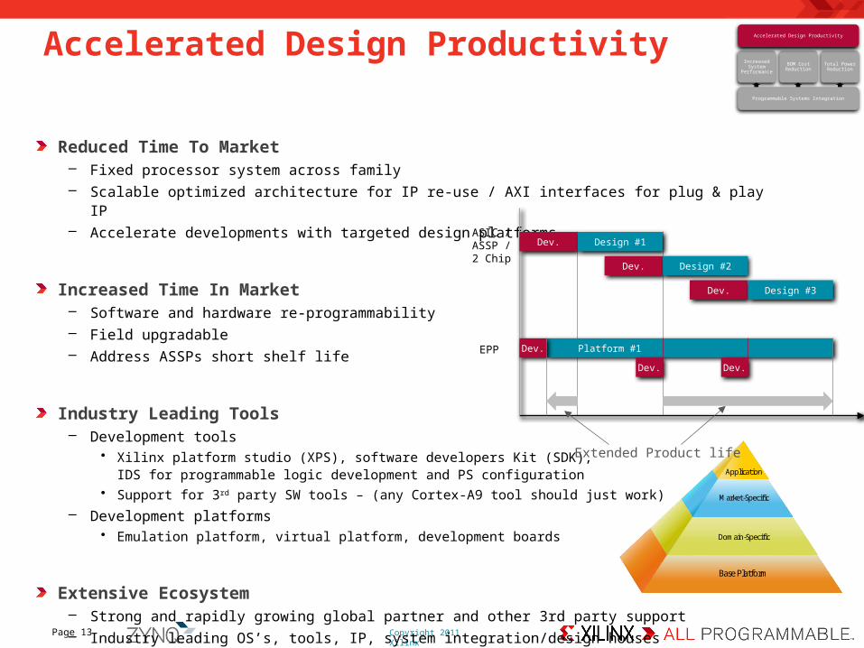
Reduced Time To Market– Fixed processor system across family– Scalable optimized architecture for IP re-use / AXI interfaces for plug & play IP– Accelerate developments with targeted design platforms
Increased Time In Market– Software and hardware re-programmability– Field upgradable– Address ASSPs short shelf life
Industry Leading Tools– Development tools
• Xilinx platform studio (XPS), software developers Kit (SDK), IDS for programmable logic development and PS configuration
• Support for 3rd party SW tools – (any Cortex-A9 tool should just work)
– Development platforms• Emulation platform, virtual platform, development boards
Extensive Ecosystem – Strong and rapidly growing global partner and other 3rd party support– Industry leading OS’s, tools, IP, system integration/design houses Base Platform
Domain-Specific
Market-Specific
Application
Programmable Systems Integration
Increased System Performance
BOM Cost Reduction
Total Power Reduction
Accelerated Design Productivity
Dev. Design #1
Platform #1
Dev.
Dev.
Dev.
Design #3
Design #2
Dev. Dev.
ASIC /ASSP /2 Chip
EPP
Extended Product life
Page 13
Copyright 2011 Xilinx© Copyright 2009 XilinxCopyright 2011 Xilinx
Zynq-7000 EPP Value Proposition
Page 14
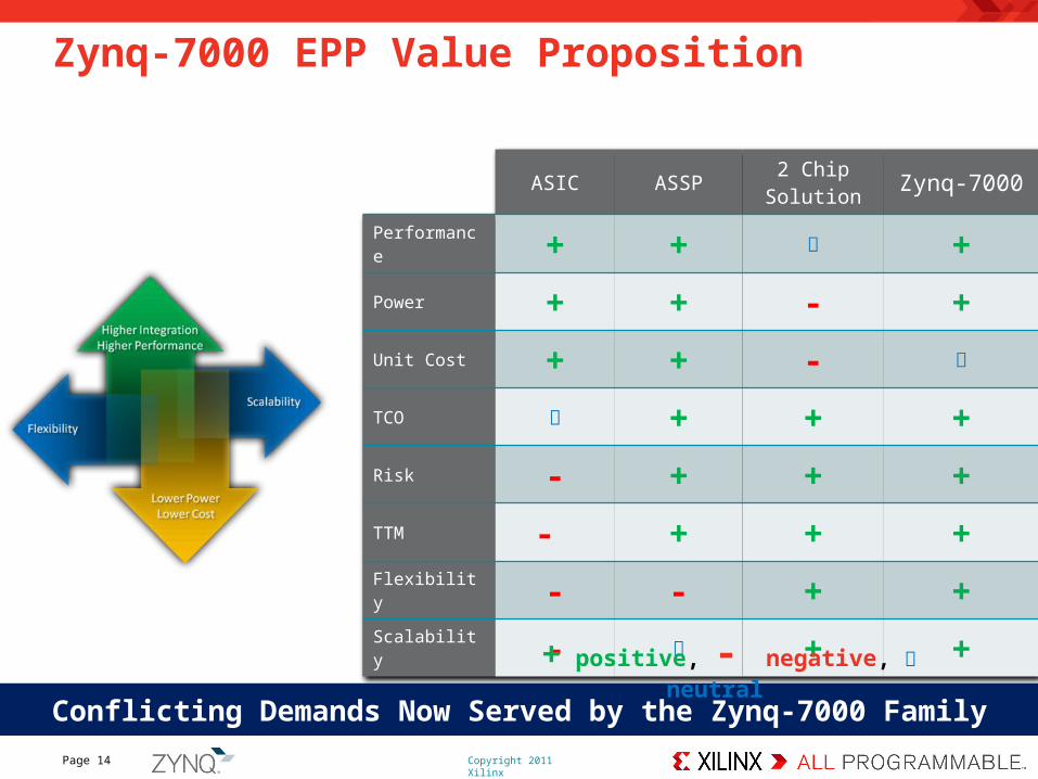
ASIC ASSP2 Chip
Solution Zynq-7000
Performance + + +Power + + - +Unit Cost + + -
TCO + + +Risk - + + +TTM - + + +Flexibility - - + +Scalability - + +
Conflicting Demands Now Served by the Zynq-7000 Family
+ positive, - negative, neutral

© Copyright 2009 XilinxCopyright 2011 Xilinx
Designing with Zynq-7000 EPP

Copyright 2011 Xilinx© Copyright 2009 XilinxCopyright 2011 XilinxCopyright 2011 Xilinx
Zynq-7000 EPP Platform Offering
SW DevelopmentTools
Ref
eren
ce D
esig
n &
Boa
rd
HW DevelopmentToolsSW & HW IP
Applications
OS KernelHigh Level and Low Level Drivers
Processing SystemProgrammable
Logic
OS
BS
P’s
Sili
con
Custom
Libraries & APIs
Virt
ual P
latfo
rm
More Than Just Silicon – A Comprehensive Platform Offering.
Page 16
Copyright 2011 Xilinx© Copyright 2009 XilinxCopyright 2011 XilinxCopyright 2011 Xilinx
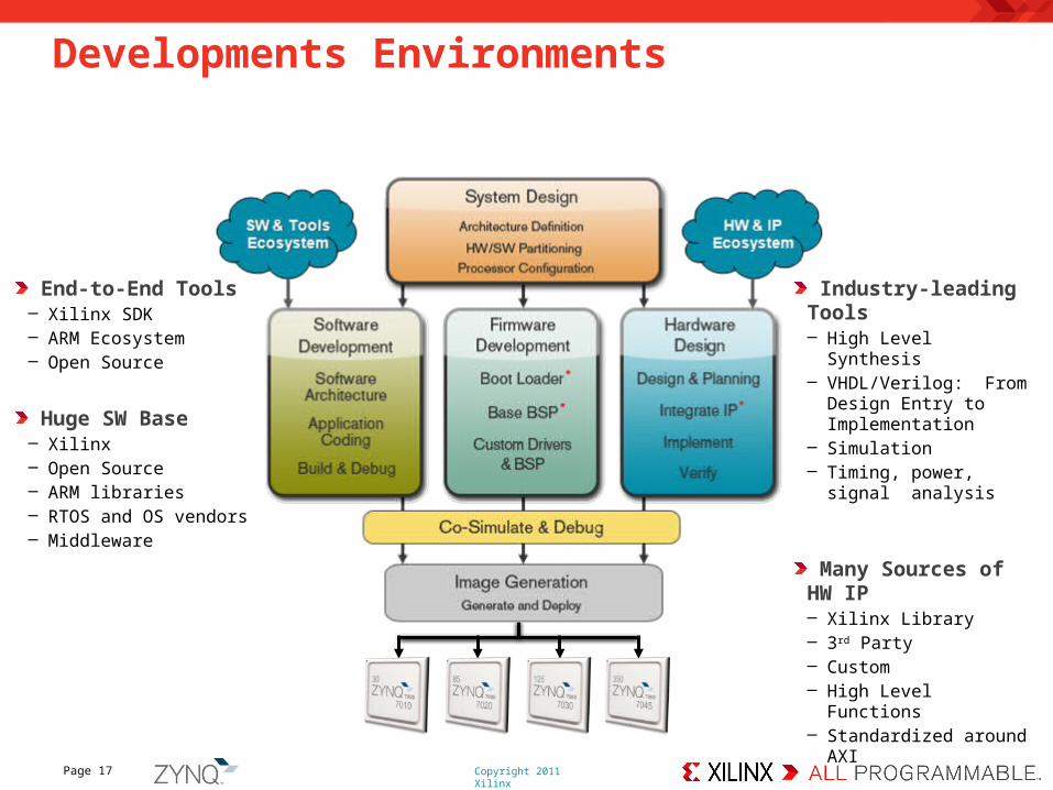
Developments Environments
Page 17
Industry-leading Tools– High Level Synthesis– VHDL/Verilog: From
Design Entry to Implementation
– Simulation– Timing, power, signal
analysis
Many Sources of HW IP– Xilinx Library– 3rd Party– Custom– High Level Functions– Standardized around AXI
End-to-End Tools– Xilinx SDK– ARM Ecosystem– Open Source
Huge SW Base– Xilinx– Open Source– ARM libraries– RTOS and OS vendors– Middleware

Copyright 2011 Xilinx© Copyright 2009 XilinxCopyright 2011 XilinxCopyright 2011 Xilinx
Zynq-7000 EPP SW Development Environment
ARM-standard Development with Xilinx Flexibility– Standard ARM Instruction Set and APIs– AXI support– Easy software migration from
other ARM-based systems
Leverage ARM Worldwide Ecosystem– Tools– OS, Middleware, Libraries– Professional Services– 3rd Party– Open Source Community
Board Support Package, Drivers and Custom IP Cores– Provided for a range of development boards, peripherals
and system functions
Page 18
Applications
OS KernelHigh Level and Low Level Drivers
Processing System Programmable Logic
OS
BS
P’s
Sili
con
Custom
Libraries & APIs

Copyright 2011 Xilinx© Copyright 2009 XilinxCopyright 2011 XilinxCopyright 2011 Xilinx
Applications
OS KernelHigh Level and Low Level Drivers
Processing System Programmable Logic
OS
BS
P’s
Sili
con
Custom
Libraries & APIs
Zynq-7000 EPP HW Design Environment
Customize your Design– Create a unique microprocessor configuration– Realize DSP, graphics, communications functions– Design custom accelerators and functions– Deploy high level functions directly to silicon
Xilinx-Optimized EDA Design tools– HDL & HLS simulation– HDL synthesis– Design analysis
Integrate Plug & Play IP Portfolio– AMBA® AXI enabled– Large selection of Xilinx and 3rd Party IP
Page 19
Copyright 2011 Xilinx© Copyright 2009 XilinxCopyright 2011 XilinxCopyright 2011 Xilinx
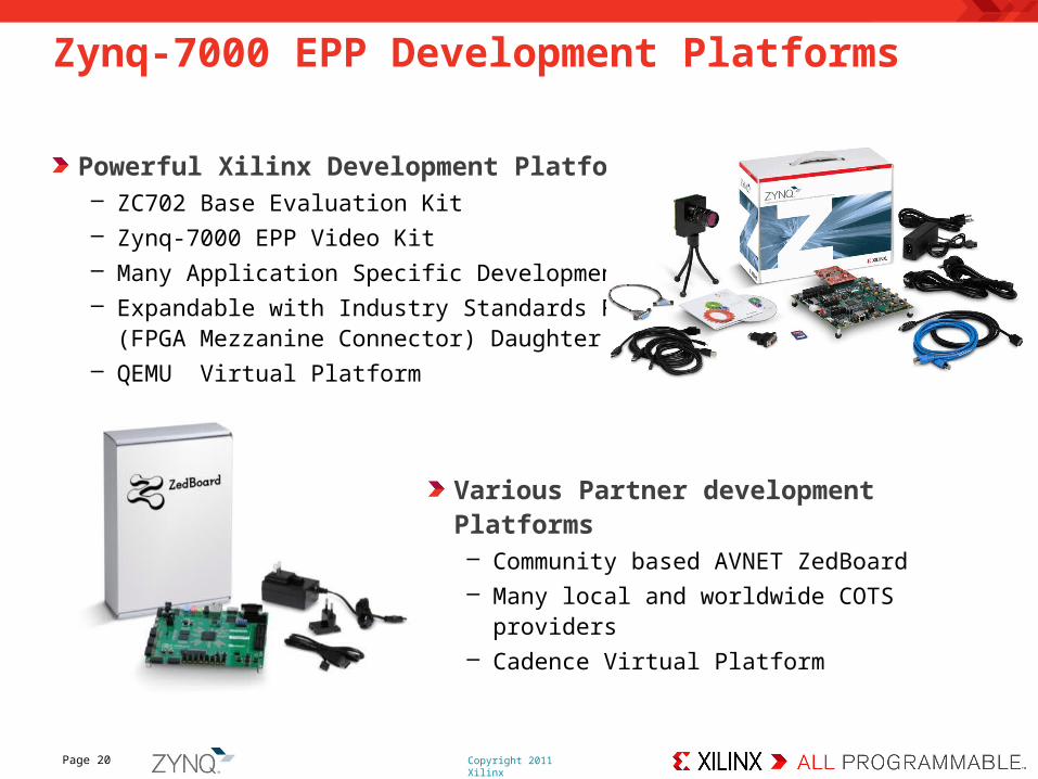
Powerful Xilinx Development Platforms– ZC702 Base Evaluation Kit– Zynq-7000 EPP Video Kit – Many Application Specific Development Kits– Expandable with Industry Standards FMC
(FPGA Mezzanine Connector) Daughter Cards– QEMU Virtual Platform
Various Partner development Platforms– Community based AVNET ZedBoard– Many local and worldwide COTS providers– Cadence Virtual Platform
Page 20
Zynq-7000 EPP Development Platforms

Copyright 2011 Xilinx© Copyright 2009 XilinxCopyright 2011 XilinxCopyright 2011 XilinxPage 21
Extensive Partnership Ecosystem
And MORE …
Copyright 2011 Xilinx© Copyright 2009 XilinxCopyright 2011 XilinxCopyright 2011 XilinxPage 22
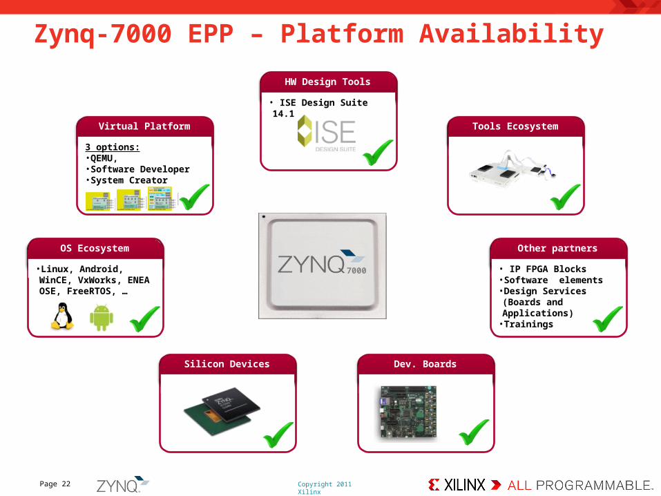
Zynq-7000 EPP – Platform Availability
7000
HW Design Tools
• ISE Design Suite 14.1
Tools Ecosystem
OS Ecosystem
•Linux, Android, WinCE, VxWorks, ENEA OSE, FreeRTOS, …
Virtual Platform
3 options:•QEMU, •Software Developer•System Creator
Other partners
• IP FPGA Blocks•Software elements•Design Services (Boards and Applications)
•Trainings
Dev. BoardsSilicon Devices
Copyright 2011 Xilinx© Copyright 2009 XilinxCopyright 2011 XilinxCopyright 2011 Xilinx
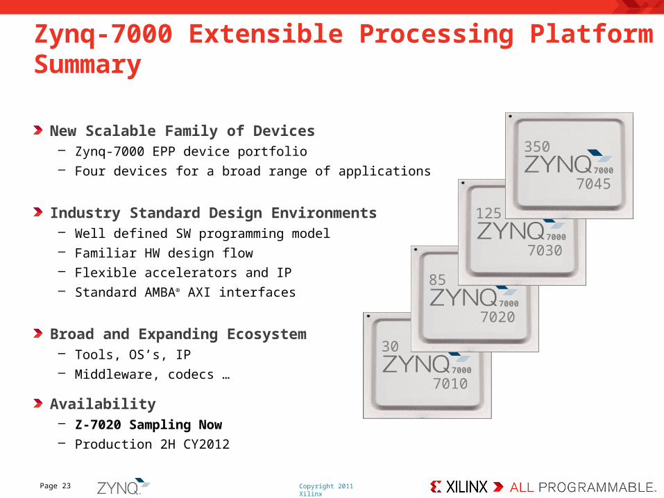
New Scalable Family of Devices– Zynq-7000 EPP device portfolio– Four devices for a broad range of applications
Industry Standard Design Environments– Well defined SW programming model– Familiar HW design flow– Flexible accelerators and IP– Standard AMBA® AXI interfaces
Broad and Expanding Ecosystem– Tools, OS’s, IP– Middleware, codecs …
Availability– Z-7020 Sampling Now– Production 2H CY2012
Page 23
Zynq-7000 Extensible Processing Platform Summary
7000
7010
30
7000
7020
85
7000
7030
125
7000
7045
350

Copyright 2011 Xilinx© Copyright 2009 XilinxCopyright 2011 XilinxCopyright 2011 Xilinx
Zynq-7000 EPP Driver Assistance Application
Page 24

Copyright 2011 Xilinx© Copyright 2009 XilinxCopyright 2011 XilinxCopyright 2011 Xilinx
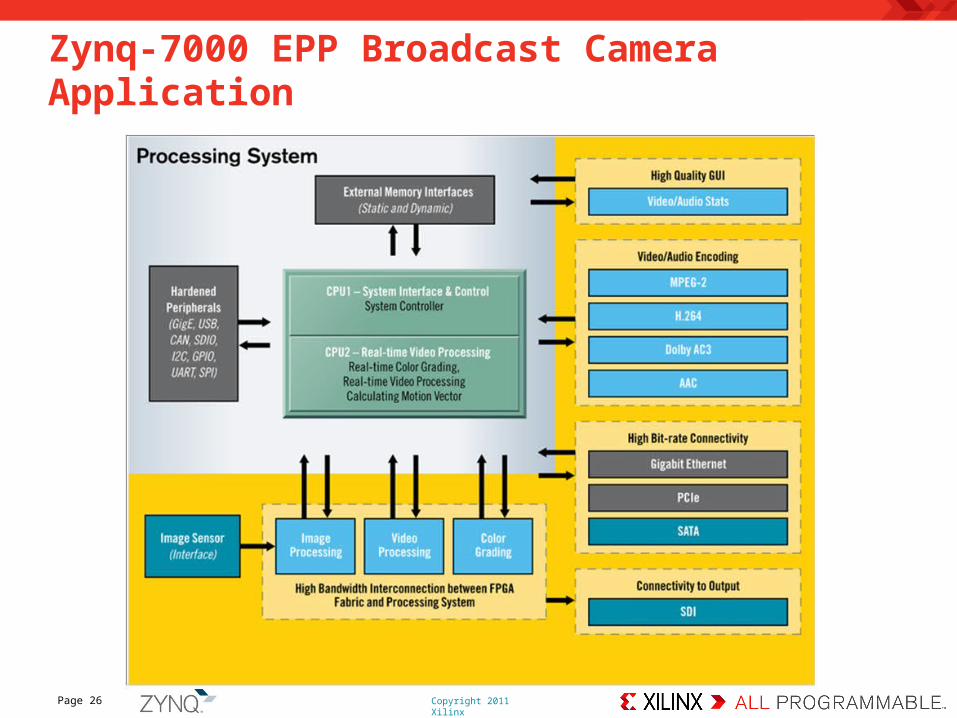
Zynq-7000 EPP Broadcast Camera Application
Page 25
Copyright 2011 Xilinx© Copyright 2009 XilinxCopyright 2011 XilinxCopyright 2011 Xilinx
Zynq-7000 EPP Broadcast Camera Application
Page 26
© Copyright 2009 XilinxCopyright 2011 Xilinx
Device Table
Copyright 2011 Xilinx© Copyright 2009 XilinxCopyright 2011 XilinxCopyright 2011 XilinxPage 28
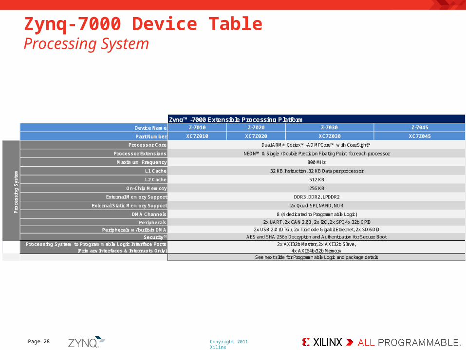
Zynq-7000 Device TableProcessing System
Device Name
Part Number
Processor Core
Processor Extensions
Maximum Frequency
L1 Cache
L2 Cache
On-Chip Memory
External Memory Support
External Static Memory Support
DMA Channels
Peripherals
Peripherals w/ built-in DMA
Security(1)
Processing System to Programmable Logic Interface Ports (Primary Interfaces & Interrupts Only)
See next slide for Programmable Logic and package details
XC7Z010 XC7Z020 XC7Z030 XC7Z045
Pro
cess
ing
Sys
tem
2x USB 2.0 (OTG), 2x Tri-mode Gigabit Ethernet, 2x SD/SDIO
AES and SHA 256b Decryption and Authentication for Secure Boot
Z-7010 Z-7020 Z-7030 Z-7045
2x AXI 32b Master, 2x AXI 32b Slave,4x AXI 64b/32b Memory
DDR3, DDR2, LPDDR2
2x Quad-SPI, NAND, NOR
8 (4 dedicated to Programmable Logic)
2x UART, 2x CAN 2.0B, 2x I2C, 2x SPI, 4x 32b GPIO
Zynq™-7000 Extensible Processing Platform
Dual ARM® Cortex™-A9 MPCore™ w ith CoreSight™
NEON™ & Single / Double Precision Floating Point for each processor
800 MHz
32 KB Instruction, 32 KB Data per processor
512 KB
256 KB

Copyright 2011 Xilinx© Copyright 2009 XilinxCopyright 2011 XilinxCopyright 2011 XilinxPage 29
Zynq-7000 Device TableProgrammable Logic and Packages
Device Name
Part Number
Xilinx 7 Series Programmable Logic Equivalent
Programmable Logic Cells (Approximate ASIC Gates (3))
Look-Up Tables (LUTs)
Flip-Flops
Extensible Block RAM (# 36 Kb Blocks)
Programmable DSP Slices (18x25 MACCs)
Peak DSP Performance (Symmetric FIR)
PCI Express® (Root Complex or Endpoint)
Agile Mixed Signal (AMS) / XADC
Security(1)
Commercial (0C to 85C)
Extended (0C to 100C)
Industrial (-40C to 100C)
Package Type (4) CLG400 CLG484 FBG484 FBG676 FFG676 FBG676 FFG676 FFG900
Size (mm) 17x17 19x19 23x23 27x27 27x27 27x27 27x27 31x31
Pitch (mm) 0.8 0.8 1.0 1.0 1.0 1.0 1.0 1.0
Processing System User I/Os (Excludes DDR dedicated I/Os)(2) 54 54 54 54 54 54 54 54
Multi-Standards and Multi-Voltage SelectIOTM Interfaces(1.2V, 1.35V, 1.5V, 1.8V, 2.5V, 3.3V)
125 200 100 100 100 100 100 212
Multi-Standards and Multi-Voltage High Performance SelectIO Interfaces
(1.2V, 1.35V, 1.5V, 1.8V)— — 63 150 150 150 150 150
Serial Transceivers — — 4 4 4 8 8 16
Maximum Transceiver Speed (Speedgrade Dependant) N/A N/A 6.6 Gb/s 6.6 Gb/s 12.5 Gb/s 6.6 Gb/s 12.5 Gb/s 12.5 Gb/s
Notes: 1. Security block is shared by the Processing System and the Programmable Logic.
2. Static memory interface combined w ith the usage of many peripherals could require more than 54 I/Os. In that case the designer can use the Programmable Logic SelectIO interface.
3. Eqivalent ASIC gate count is dependent of the function implemented. The assumption is 1 Logic Cell = ~15 ASIC Gates.
4. Devices in the same package are pin to pin compatible, FBG676 and FFG676 are also pin to pin compatible
5. Preliminary product information. Subject to change. Please contact your Xilinx representative for the latest information
XC7Z010 XC7Z020 XC7Z030 XC7Z045
Zynq™-7000 Extensible Processing PlatformZ-7010 Z-7020 Z-7030 Z-7045
35,200 106,400 157,200 437,200
Pro
gra
mm
able
Lo
gic
Artix™-7 FPGA Artix™-7 FPGA Kintex™-7 FPGA Kintex™-7 FPGA
28K Logic Cells (~430K) 85K Logic Cells (~1.3M) 125K Logic Cells (~1.9M) 350K Logic Cells (~5.2M)
17,600 53,200 78,600 218,600
240 KB (60) 560 KB (140) 1,060 KB (265) 2,180 KB (545)
80 220 400 900
58 GMACS 158 GMACS 480 GMACS 1080 GMACS
— — Gen2 x4 Gen2 x8
Pac
kag
es
2x 12 bit, MSPS ADCs w ith up to 17 Differential Inputs
AES and SHA 256b Decryption and Authentication for Secure Programmable Logic Configuration
Sp
eed
G
rad
es
-1
-2, -3
-1, -2
CLG400
17x17
0.8
54
100
—
—
N/A