© 2008 tienyu chang - university of...
TRANSCRIPT

1
DESIGN OF WIDEBAND COMMUNICATION CIRCUITS
By
TIENYU CHANG
A DESSERTATION PRESENTED TO THE GRADUATE SCHOOL OF THE UNIVERSITY OF FLORIDA IN PARTIAL FULFILLMENT
OF THE REQUIREMENTS FOR THE DEGREE OF DOCTOR OF PHILOSOPHY
UNIVERSITY OF FLORIDA
2008

2
© 2008 Tienyu Chang

3
ACKNOWLEDGMENTS
I would like to express my deepest gratitude to my advisor Dr. Jenshan Lin. He provides
me a research environment with free thinking and he lets me to explore what my interests are.
Without his support and guidance, I can hardly finish this doctorial study. I would also like to
thank my committee members, Dr. Rizwan Bashirullah, Dr. William Eisenstadt, and Dr. Fan Ren.
They gave me a lot of precious comments during the defense and proposal to make my study
more complete. I specially thank Mrs. Wenhsing Wu for her help during the first couple of years
fabrication and bond-wiring the GaN devices; and Dr. Fan Ren for his generous offering of his
lab equipments for testing and bond wiring.
For the several years that I’ve lived in Florida, I would like to thank all of my lab mates for
their companies and supports. Some of them are already graduated (Xiuge Yang, Yanming Xiao,
Ashok Verma, SangWon Ko, and Hyeopgoo Yeo), and some of them are still here (Lance Covert,
Mingqi Chen, Fu-Yi Han, Zhen-Ning Low, Changzhi Li, Yan Yan, Austin Chen, and Mingkai
Mu). Of course, there are some visitors from Taiwan (Ching-Ku Liao, Chih-Ming Wang, and
Jian-Ming Wu). With them, I had a great time here in Florida.
I would like to thank my parents, my brother and sister for their un-conditional
encouragement and supports. At last, in several years, my love Yu-Ping Huang has taken care of
me and supported me no matter what. This dissertation belongs to all of you.

4
TABLE OF CONTENTS page
ACKNOWLEDGMENTS ...............................................................................................................3
LIST OF TABLES...........................................................................................................................7
LIST OF FIGURES .........................................................................................................................8
ABSTRACT...................................................................................................................................14
CHAPTER
1 INTRODUCTION ..................................................................................................................16
1.1 A Brief Historical Sketch of Ultra-Wideband (UWB) Technology .................................18 1.2 Brief Review on UWB Technology .................................................................................18
1.2.1 Pulse-Based UWB Systems....................................................................................19 1.2.2 Multiband Orthogonal Frequency Division Multiplexing (MB-OFDM) UWB.....20
1.3 Design Challenges and Scope of This Study....................................................................21 1.4 Outline of the Dissertation................................................................................................24
2 PASSIVE COMPONENTS ....................................................................................................25
2.1 Inductors ...........................................................................................................................25 2.1.1 In CMOS 0.18 μm Technology ..............................................................................25 2.1.1 In CMOS 90 nm Technology .................................................................................26
2.2 Capacitors .........................................................................................................................30 2.3 Varactors...........................................................................................................................31
3 DESIGN OF WIDEBAND LOW NOISE AMPLIFIERS (LNAs) ........................................34
3.1 Topology Survey ..............................................................................................................34 3.1.1 Bandpass Filter Input Matching .............................................................................35 3.1.2 Distributed Amplifier .............................................................................................36 3.1.3 Common Gate Amplifier........................................................................................38 3.1.4 Resistive Feedback Amplifier ................................................................................38
3.2 Theoretical Analysis .........................................................................................................39 3.2.1 Basic Structure of Resistive Feedback Amplifiers .................................................39 3.2.2 R-C Feedback through a Source Follower .............................................................41 3.2.3 Input Gate Feedback Inductor ................................................................................45 3.2.4 Active Inductor Load..............................................................................................47 3.2.4 Noise Analysis........................................................................................................49 3.2.5 Bond Wires and ESD Diodes .................................................................................51 3.2.6 Neutralization Capacitors .......................................................................................53

5
3.3 Circuit Design of Proposed LNAs....................................................................................53 3.3.1 TSMC Digital 90 nm CMOS Technology..............................................................54 3.3.2 ESD Diodes ............................................................................................................54 3.3.3 LNA 1.....................................................................................................................55 3.3.4 LNA 2.....................................................................................................................57 3.3.5 LNA 3.....................................................................................................................58
3.4 Measurement Results of Proposed LNAs.........................................................................59 3.4.1 The Resistive Load UWB LNA (LNA 1)...............................................................60 3.4.2 The High Gain Wideband LNA (LNA 2)...............................................................63 3.4.3 The Active Inductor Load UWB LNA (LNA 3) ....................................................66
3.5 Conclusions.......................................................................................................................69
4 DESIGN OF WIDEBAND PASSIVE MIXERS....................................................................71
4.1 GaN Passive Mixers .........................................................................................................71 4.1.1 Modeling of GaN Transistors in the Linear Region...............................................72 4.1.2 Design of GaN Resistive Mixers............................................................................75 4.1.3 Measurement Results..............................................................................................76
4.2 CMOS Passive Mixer .......................................................................................................80 4.2.1 Discussion on CMOS Resistive Ring Mixer ..........................................................80 4.2.2 Design of CMOS Resistive Ring Mixer.................................................................84 4.2.3 Simulation and Measurement Results ....................................................................86
4.3 CMOS Passive Harmonic Pumped Mixer ........................................................................90 4.3.1 Discussions on Each Block ....................................................................................91 4.3.2 Measurement Results of the Resistive Harmonic Mixer ......................................100
4.4 Conclusions.....................................................................................................................102
5 CONSIDERATION AND DESIGN OF AN UWB FREQUENCY SYNTHESIZER.........105
5.1 A Switching Band Voltage Controlled Oscillator (VCO) ..............................................105 5.1.1 Design of the Switching Band VCO ....................................................................106 5.1.2 Experimental Results............................................................................................110
5.2 Introduction to MB-OFDM UWB Frequency Synthesizers...........................................113 5.2.1 PLL with an Ultra Fast Settling Time ..................................................................116 5.2.2 Switching Between Multiple PLLs ......................................................................119 5.2.3 Switching Between Different Frequencies Using Mixers ....................................121
5.3 The Proposed OFDM UWB Frequency Synthesizers ....................................................121 5.3.1 Effect of Spurious Signals in Frequency Synthesizers on BER performance......122 5.3.2 Scheme of Frequency Generation ........................................................................125 5.3.3 Block Diagram of the Frequency Synthesizer......................................................127
5.4 Spurious Signals from the Frequency Synthesizers........................................................128 5.4.1 Spurious Signals from Mixers ..............................................................................128 5.4.2 Subharmonic Mixers ............................................................................................129 5.4.3 Filtering Out the Spurious Signals .......................................................................131 5.4.4 Square Wave Harmonic Reduction ......................................................................136 5.4.5 Implementation of a Harmonic Reduction Circuit ...............................................139
5.5 Schematics and Simulation Results ................................................................................143

6
5.6 Conclusions.....................................................................................................................145
6 SUMMARY AND FUTURE WORKS ................................................................................146
6.1 Summary.........................................................................................................................146 6.2 Future Works ..................................................................................................................147
REFERENCES ............................................................................................................................149
BIOGRAPHICAL SKETCH .......................................................................................................154

7
LIST OF TABLES
Table page 1-1 Various data rates of the MB-OFDM UWB system..........................................................22
3-1 Measured performance compared with prior published works..........................................70
4-1 Summary of the GaN resistive mixers ...............................................................................79
4-2 Summary of the III-V resistive mixers from existing publications ...................................80
4-3 Summarize of the fundamental passive mixer and the subharmonic passive mixer........104
5-1 Performance summary of the band switching VCO ........................................................113
5-2 Center frequencies plan for OFDM UWB.......................................................................114
5-3 Operating distances for OFDM UWB system with different channel conditions and date rate............................................................................................................................115
5-4 Relation of LO frequencies of different bands ................................................................126

8
LIST OF FIGURES
Figure page 1-1 WPAN technologies with different usable range and data rate. ........................................17
1-2 FCC regulation of UWB spectral mask for indoor communication systems.....................19
1-3 UWB pulse waveforms ......................................................................................................20
1-4 Spectrum utilizing plan for the MB-OFDM UWB system................................................20
1-5 Scope diagram of this doctorial research. ..........................................................................23
2-1 Cross section diagram of a TSMC 1P6M 0.18 µm mixed-mode CMOS process. ............26
2-2 Physical diagram of a differential inductors in HFSS. ......................................................27
2-3 Model used for differential inductors. ...............................................................................27
2-4 Fitting results of a differential inductor in 0.18 µm CMOS ..............................................28
2-5 Side-view of a multi-layered inductor in a 90 nm CMOS technology. .............................28
2-6 HFSS diagrams of a stacked differential inductor in a 90 nm CMOS technology with w=6 µm, r=130 µm, and s=2 µm.HFSS diagram of a stacked differential inductor in a 90 nm CMOS technology................................................................................................29
2-7 Simulation results of a 2 nH differential inductor in a 90 nm CMOS technology.. ..........29
2-8 MIM capacitor’s graphs.....................................................................................................30
2-9 Top views of an interdigital capacitor. ..............................................................................31
2-10 Cross section of an A-MOS varactor.. ...............................................................................32
2-11 Simulated capacitance values versus biasing voltages of an A-MOS varactor. ................32
2-12 Cross-section view of an I-MOS varactor. ........................................................................33
2-13 Simulated capacitance values versus biasing voltages of an I-MOS varactor...................33
3-1 Results of an input matching wideband LNA from Bevilacqua, etc. ................................35
3-2 Results of the distributed LNA. .........................................................................................36
3-3 Results of the common gate LNA......................................................................................37
3-4 Results of the resistive feedback LNA...............................................................................39

9
3-5 Basic structure of a resistive feedback amplifier. ..............................................................40
3-6 Schematic of a resistive feedback amplifier feeding back through a source follower.......41
3-7 Small signal equivalent model of the circuit in Figure 3-6................................................42
3-8 Simulation results of the effects of load capacitance CL on input impedance for a resistive feedback amplifier. ..............................................................................................43
3-9 Simulation results of the effects of Cf on input impedance for a resistive feedback amplifier. ............................................................................................................................44
3-10 Schematic of a resistive feedback amplifier feeding back with a peaking inductor inside the feedback loop.....................................................................................................46
3-11 Trajectories of pole locations with increasing value of gate inductor in resistive feedback amplifier. ............................................................................................................47
3-12 Simulation results of the voltage gain versus frequency using equation (3-7). .................48
3-13 An active inductor load’s graphs .......................................................................................48
3-14 Frequency response of magnitude of input impedance......................................................49
3-15 Equivalent model of wideband LNA’s input stage with package and ESD diodes added. .................................................................................................................................51
3-16 Smith Chart of S11 simulation results from DC to 15 GHz................................................52
3-17 Layout of ESD diodes........................................................................................................54
3-18 Schematic of LNA 1 (biasing circuits not shown).............................................................55
3-19 Schematic of LNA 2 (biasing circuits not shown).............................................................57
3-20 Schematic of LNA 3 (biasing circuits not shown).............................................................59
3-21 Chip photo of LNA1 (area=0.58mm x 0.22mm with pad). ...............................................60
3-22 Measurement (solid line) and simulation (dashed line) results of voltage gain for LNA1. ................................................................................................................................61
3-23 Measurement (solid line) and simulation (dashed line) results of S11 for LNA1. .............61
3-24 Measurement results of S22 and S12 for LNA1...................................................................62
3-25 Measurement (solid line) and simulation (dashed line) results of NF for LNA1. .............62
3-26 Measured linearity results for LNA1. ................................................................................63

10
3-27 Chip photo of LNA2 (area=0.56mm x 0.42mm with pad). ...............................................64
3-28 Measurement (solid line) and simulation (dashed line) results of voltage gain for LNA2. ................................................................................................................................64
3-29 Measurement (solid line) and simulation (dashed line) results of S11 for LNA2. .............65
3-30 Measurement results of S22 and S12 for LNA2...................................................................65
3-31 Measurement (solid line) and simulation (dashed line) results of NF for LNA2. .............66
3-32 Measured linearity results for LNA2. ................................................................................66
3-33 Chip photo of the LNA 3 (area=0.38mm x 0.36mm with pad). ........................................67
3-34 Measurement (dotted line) and simulation (dashed line) results of voltage gain for LNA3. ................................................................................................................................67
3-35 Measurement (dotted line) and simulation (dashed line) results of S11 for LNA3...........68
3-36 Measured results of S12 and S22 for LNA3......................................................................68
3-37 Measurement (dots) and simulation (dashed line) results of NF for LNA3. .....................69
3-38 Measured linearity results for LNA3. ................................................................................69
4-1 Die photo of one of the GaN HEMT devices with a device area of 200 μm x 1 μm.........72
4-2 Equivalent circuit model used for GaN HEMT devices. ...................................................73
4-3 Modeled Rds versus gate bias on GaN devices with different gate lengths. ......................74
4-4 Measured and simulated conversion loss versus LO power for GaN devices with different gate lengths..........................................................................................................75
4-5 Schematic of the single-FET resistive mixer. ....................................................................76
4-6 Photo of the GaN mixer board. ..........................................................................................77
4-7 Measured conversion loss versus RF frequency................................................................78
4-8 Measured conversion loss versus RF power. .....................................................................78
4-9 Two-tone IIP3 measurement result of the GaN resistive mixers.......................................79
4-10 Schematics of the resistive mixer. .....................................................................................81
4-11 Conversion loss versus frequency of CMOS resistive mixers with different gate lengths. ...............................................................................................................................82

11
4-12 Schematic of the wideband resistive ring mixer. ...............................................................84
4-13 Chip photo of the fabricated mixer (chip size including the pads: 0.95 mm x 0.65 mm). ...................................................................................................................................85
4-14 Measurement and simulation results of conversion loss versus RF frequency with fixed IF frequency 500 MHz..............................................................................................86
4-15 Input P1dB and IIP3 versus RF frequency. .......................................................................88
4-16 Measurement results of conversion loss versus LO power. The measurements were conducted for ten RF frequencies from 1 GHz to 10 GHz. ...............................................88
4-17 Measurement results of the RF return loss from 100 MHz to 12 GHz..............................89
4-18 Measurement results of the NF of the wideband passive mixer. .......................................89
4-19 Systematic blocks of the subharmonic mixer with an integrated VCO. ............................91
4-20 A 5 GHz VCO’s diagrams. ................................................................................................92
4-21 Schematic of a current mode divide-by-2 circuit...............................................................93
4-22 Simulation results of the divider input and output.............................................................94
4-23 Variation of channel resistance..........................................................................................94
4-24 Variation in conductance ...................................................................................................95
4-25 Schematic of a resistive harmonic double balanced mixer. ...............................................96
4-26 Transient simulation of input and output. ..........................................................................96
4-27 Output spectrums of the subharmonic mixer. ....................................................................98
4-28 Different RF input biasing levels with differential LO signals..........................................99
4-29 Simulation results of a subharmonic passive mixer with different RF bias conditions.....99
4-30 Die photo with an area of 0.85mm × 0.7mm. ..................................................................100
4-31 Effects of RF bias on the conversion loss of the mixer. ..................................................101
4-32 Measurement and simulation results of conversion gain of the mixer. ...........................101
4-33 Measured LO leakage to the IF and RF ports with varying LO frequency. ....................102
4-34 Measured P1dB, IIP2, and IIP3 of the passive subharmonic mixer. ...............................103

12
5-1 Schematic of the switching band VCO............................................................................107
5-2 Schematic of resonant tank. .............................................................................................109
5-3 Die photo of the switching band VCO.............................................................................110
5-4 Measured conversion loss versus offset frequency..........................................................111
5-5 The tuning capability of the switching band VCO. .........................................................112
5-6 Frequency plan chart of the OFDM UWB.......................................................................114
5-7 Frequency hopping diagram between the different bands. ..............................................116
5-8 Block diagram of an integral-N frequency synthesizer. ..................................................116
5-9 Block diagram with mathematical modeling of integral-N PLL. ....................................117
5-10 Settling behaviors of a fast switching PLL. .....................................................................118
5-11 A MB-OFDM UWB frequency synthesizer using multiple PLLs...................................119
5-12 A MB-OFDM UWB frequency synthesizer using two swapping PLLs..........................120
5-13 Two implementation of MB-OFDM UWB frequency synthesizers................................121
5-14 Spurious signals of a frequency synthesizer. ...................................................................122
5-15 Simulation diagram of effect on BER due to spurious signals in a frequency synthesizer........................................................................................................................123
5-16 Simulation result of BER with various spurious signal levels.........................................124
5-17 Testing environment of the spurious signal test. .............................................................125
5-18 Scheme of the frequency generation for a MB-OFDM UWB frequency synthesizer. ....127
5-19 Block diagram of the MB-OFDM UWB frequency generator. .......................................128
5-20 Spurious signals from a mixer. ........................................................................................129
5-21 Load of a subharmonic mixer. .........................................................................................130
5-22 Single-side-band mixers with imbalanced inputs. ...........................................................132
5-23 Signal isolation of SSB mixer due to imbalanced inputs.................................................133
5-24 Filter of the outputs of a SSB mixer. ...............................................................................133
5-25 A polyphase filter’s diagrams. .........................................................................................134

13
5-26 Simulation result of a three-stage polyphase filter. .........................................................135
5-27 Polyphase filter with a single-side-band mixer................................................................136
5-28 Simulation results show the effect of a polyphase filter. .................................................136
5-29 Harmonics of a square wave. ...........................................................................................137
5-30 Effect of square wave harmonics on SSB mixers. ...........................................................138
5-31 Square waves with different 45o phase differences and the resulting waveform after summation........................................................................................................................138
5-32 Using ring oscillator to generate multiphase signals. ......................................................140
5-33 Use a divider to generate quadrature signals ...................................................................140
5-34 Cascade dividers for 45o phase difference. ......................................................................141
5-35 The phase detection circuitry. ..........................................................................................142
5-36 Phase detection circuit after divide-by-2 blocks..............................................................142
5-37 Schematic of the MB-OFDM UWB frequency synthesizer. ...........................................143
5-38 Simulation results showing the transition time switching from one band to the other....144
5-39 Simulation results showing the spectrum of the signal before the transition, and the spectrum of the signal after the transition........................................................................145

14
Abstract of Dissertation Presented to the Graduate School of the University of Florida in Partial Fulfillment of the Requirements for the Degree of Doctor of Philosophy
DESIGN OF WIDEBAND COMMUNICATION CIRCUITS
By
Tienyu Chang
May 2008
Chair: Jenshan Lin Major: Electrical and Computer Engineering
The wideband wireless communication system (e.g. Ultra-Wideband (UWB)) is becoming
popular for its capability to achieve high data rate wireless transmission. With the progress on
CMOS technology in recent years, it could achieve comparable performances at high frequencies
to other compound materials (e.g. GaAs) but with much lower cost. Therefore, implementing
wideband circuits using CMOS technology has become one of the most important topics in the
RF circuit design.
In this study, several wideband CMOS circuits along a receiver chain were designed and
tested using various novel design techniques. Low noise amplifiers (LNAs) are one of the most
critical components in a receiver design. Three LNAs were designed and measured using a 90
nm CMOS technology. The LNAs adopt a modified resistive feedback topology for wideband
input matching and gain-bandwidth extension. All of the LNAs were measured with chip-on-
board package and electrostatic discharge (ESD) protection diodes at all the ports. Two of the
LNAs were designed for the UWB application and one of the LNA was designed for the multi-
band application. Tradeoffs between the noise figure (NF), bandwidth, and gain will be
demonstrated in the proposed LNAs.

15
Mixers are also of focus in this doctorial research. Several wideband passive mixers were
designed and tested. At first, board level mixers using GaN devices were designed and measured.
GaN devices have the property of high breakdown voltage. Therefore, they can be used in high
power and high linearity applications. The transistors were modeled specially in the linear region
to accurately estimate the performance of the passive mixers. Three passive mixers were
fabricated using GaN HEMT transistors with different gate lengths. The results show good
linearity performance.
Next, two passive mixers were designed and tested using a 0.18 μm CMOS technology. A
fundamental passive mixer and a sub-harmonic passive mixer were made. The fundamental
passive mixer achieves a very wide bandwidth for UWB devices. The sub-harmonic passive
mixer utilizes the second harmonic of the local oscillator (LO) signal achieving a high LO-IF
leakage. The chip includes a sub-harmonic mixer, a voltage controlled oscillator (VCO), and a
quadrature generation circuitry.
Finally, a wideband VCO and a UWB frequency synthesizer were considered and designed.
The switching band VCO implemented in 0.18 μm CMOS achieves a tuning range from 3 GHz
to 5 GHz. Switching inductors and capacitors were used to change the oscillating frequencies.
Next, a frequency synthesizer used for the multi-band orthogonal frequency division
multiplexing (MB-OFDM) UWB system was designed. The simulated synthesizer can generate
twelve bands ranging from 3 GHz to 10 GHz using the sub-harmonic mixing technique. Various
spurious reduction methods were implemented to reduce the interferences caused by the spurious
signals.

16
CHAPTER 1 INTRODUCTION
Wireless communication has already become part of our life in the 21st century. It started
from the cell phones in the late 20th century. At the time, only the voice data is transmitted
wirelessly through cell phones. Now people are trying to get every kind of digital data, from a
text message, to a voice clip, and even to a movie with a high resolution HDTV format, to be
transmitted through the air,
Because the differences in the natures of the signals transmitting, several standards have to
be set up for each special needs. One of which is for the Wireless Personal Area Network
(WPAN). It focuses on the development of short distance wireless networks. These networks
address wireless networking of portable and mobile computing devices such as PCs, PDAs,
peripherals, cell phones and consumer electronics. Depending on different requirements on the
transmission speed and operating range, standards that could be chosen from are list in Figure 1-
1. While the operating range needs to be high, we have standard IEEE Wireless Local Area
Network (WLAN) 802.11a/b/g/n (e.g. WiFi) working for us. While the data rate and operating
range is lower, but ultra-low power is needed to extend the battery life time, Bluetooth is at the
help. As for extremely high data rate transmissions of hundreds of mega bytes per second, Ultra-
Wideband (UWB) comes into play.
Because of the uniqueness in the extreme high data rate transmission comparing to other
communication systems, the transceiver design of the UWB systems is very different with the
rest of narrow band based communication systems and it posts a lot of interests on the design of
UWB circuits. Therefore, wideband wireless (especially UWB) communicating systems will be
the main focus in this dissertation among all the wireless communications.

17
Figure 1-1. WPAN technologies with different usable range and data rate.
The goal of an UWB system is to provide a short range but high data rate wireless
transmission. The first application of UWB technology is to replace the cables that connected
between machines in the offices or home. Cables are always bothering people for their easily get
tangled up. However, UWB is not just a cable replacement technology. With the help of UWB
technology, all of them could be connected together wirelessly. With the connectivity, we have
the ability to control all the equipments at the same time and make them working with each other.
UWB could change the way we use our electronic products. In the age of wireless
communication and interconnectivity, the UWB communication system will be integrated into
PCs. Mobile phones and handheld devices, digital cameras and camcorders as well as all many
of the consumer electronics and home entertainment systems. Using the UWB technology, they
will be able to share multimedia content with very large amount of data.
Range (m)
Data Networking
802.11a/b/g/n
802.11n promises
100Mbps @ 100m
Quality of service, streaming
Room-range High-definition
UWB
Bluetooth
UWB Short
Distance Fast download
110Mbps @ 10m
480Mbps @ 2m 200Mbps @ 4m
1000
100
10
1
1 10 100 Source: Texas Instruments
Dat
a R
ate
(Mbp
s)

18
1.1 A Brief Historical Sketch of UWB Technology
It was started at Feb 14, 2002 when Federal Communications Commission (FCC) allocated
7500 MHz of spectrum for unlicensed use for UWB devices in the 3.1 to 10.6 GHz frequency
band [2]. Prior to January 2003, the IEEE conducted study groups to investigate the possibility of
pursuing a standard based upon the new spectrum. The IEEE 802 committees setup a new
802.15.3a committee put out a call for proposals to develop WPANs. Because of the large
number of proposals makes the selection process slow.
After couple of meetings and discussions, two proposals are left to be decided. One of
which is based on Multiband OFDM technology and the other is based on direct sequence
technology. Because the fundamental technologies of the two standards are quite different, the
supporters on each side could not set a final conclusion. Furthermore, because UWB needs to be
operated over extremely short range, it is particularly vulnerable to interference. As a result, the
process became jammed for years.
Finally, the OFDM supporters elected to continue the work on standardization outside of
the IEEE 802.15.3a task group. This outside group gradually formalized their relationship and
started an organization called “Multiband OFDM Alliance” (MBOA). Eventually this group
became known as the WiMedia Alliance. As a result, technical specification development and
certification and interoperability activities are unified in the WiMedia Alliance. On January 2006,
after three years of a jammed process in IEEE 802.15.3a, supporters of both proposals supported
the shut down of the IEEE 802.15.3a task group without conclusion.
1.2 Brief Review on UWB Technology
The power spectral emission mask of the UWB systems by FCC is illustrated in Figure 1-2.
The regulation allows spectrum sharing with low emission limit (-41.3 dBm/MHz Equivalent
Isotropically Radiated Power (EIRP)) where the transmitted signal doesn’t cause harmful

19
interference to others. An UWB system is defined as any devices that emits signals with a
fractional bandwidth more than 0.2 or a bandwidth of at least 500 MHz at all time of
transmissions. There are two popular standards implementing UWB signals, one is to generate a
short pulse with wide bandwidth, and the other one is to use Multi-band Orthogonal Frequency
Division Multiplexing (MB-OFDM).
Figure 1-2. FCC regulation of UWB spectral mask for indoor communication systems.
1.2.1 Pulse-Based UWB Systems
The earliest radio implemented in the late 19th century and 20th century was the pulse-
based impulse radio. Spark gaps and arc discharges between carbon electrodes were the principal
mechanisms to produce radio signals in the early 20th century.
The pulse-based UWB signal and its spectrum are shown in Figure 1-3. An extremely short
pulse of few nano-seconds has its spectrum crossed over very wideband. The spectrum width
could be controlled by transmitting pulses with different pulse durations. The signal could be

20
modulated using several different ways including pulse-position modulation (PPM), pulse-
amplitude modulation (PAM), on-off keying (OOK), and binary phase-shift keying (BPSK). The
whole UWB spectrum could be also divided into several groups as a multiband system to reduce
interference using methods similar to frequency hopping radio.
The main advantage of pulse-based UWB system is that the transmitter has a very simple
design. Its disadvantages are that it is difficult to collect significant multi-path energy using
single RF chain; and the system is very sensitive to group delay variations introduced by analog
front-end components.
Figure 1-3. UWB pulse waveforms in (a) time domain, and in (b) frequency domain.
1.2.2 Multiband Orthogonal Frequency Division Multiplexing (MB-OFDM) UWB
Figure 1-4. Spectrum utilizing plan for the MB-OFDM UWB system.
-10 -5 0 5 10-0.5
0
0.5
1
Time (ns)
Mag
(V)
0 2 4 6 8 10-40
-30
-20
-10
0
Frequency (GHz)
Mag
(dB
)
(a) (b)

21
The standard MB-OFDM UWB utilizes all or part of the spectrum between 3.1-10.6 GHz
and supports data rates of up to 480 Mb/s. As shown in Figure 1-4, the whole UWB spectrum is
divided into 14 bands, each with a bandwidth of 528 MHz. The first 12 bands are then grouped
into 4 band groups consisting of 3 bands, and the last two bands are grouped into a fifth band
group. This multi-band technique could be used to separate the application of UWB systems to
avoid interference. The well known OFDM technique is implemented on this UWB system. A
total of 110 sub-carriers (100 data carriers and 10 guard carriers) are used per band. In addition,
12 pilot subcarriers allow for coherent detection. Frequency-domain spreading, time-domain
spreading, and forward error correction (FEC) coding are provided for optimum performance
under a variety of channel conditions.
The transmitting data rate is scalable from 55 MB/s to 480 MB/s. In realistic multi-path
environments, 110 Mb/s of data transmission could be operated within 10 meters in distance; 200
Mb/s could be operated within 4 meters in distance; and 480 Mb/s could be operated within 2
meters. Table 1-1 shows operating modes with different transmitting data rates of the MB-
OFDM UWB system. The data rate could be calculated from FsymNIBP6S/6, where Fsym is the
symbol rate which is 3.2 Msym/s for the system.
This MB-OFDM UWB standard is getting more and more popular compared to the
previous pulse-based UWB system. Therefore, MB-OFDM UWB system will be the research
topic in this PhD study. There are many good introductory papers, such as [4], [5], and [6],
describing the channel and the hardware of a MB-OFDM UWB system.
1.3 Design Challenges and Scope of This Study
The transceiver of a wideband communication system is very different from that of the
conventional narrow band systems. First of all, the design of wideband RF blocks is harder than
narrow band blocks, such as amplifier. Electronic theory tells us the gain-bandwidth product is

22
about constant. For circuits with higher bandwidth, the gain would be smaller than narrow band
ones. Therefore, multiple stages might have to cascade to boost up the gain so that the power
consumption would be higher. Performance of low cost CMOS technology is not fast enough to
have sufficient gain in the higher gigahertz region. Cost always plays the dominant role in which
technology will survive. In order to operate at that high frequency, usually huge power
consumption is needed and a lot of inductor peaking is necessary, which makes the chip size
bigger and the cost of fabrication higher. Because of this reason, most attempted commercial
UWB products are still focused on Mode 1, which covers the part of the UWB frequency
bandwidth, with frequency range from about 3 to 5 GHz.
Table 1-1. Various data rates of the MB-OFDM UWB system.
Second, because of the property in the wide frequency bandwidth, the interference is more
serious where the spurious tones fall inside the signal spectrum. The regulation from FCC states
that the power density is small compared to other narrowband systems, which means there will
be strong out-of-band blockers. Also, the UWB covers the 5 GHz band which has application as
IEEE 802.11a. There will be some coexisting issues that have to be dealt with. Some techniques
are used to overcome the interference problem such as notching out certain band as in [7].

23
Third, the fast frequency hopping is difficult to deal with. In the standard, 9 ns transition
time is required switching from one band to another. Traditional PLLs could not stabilize in this
short period of time. Switching between PLLs is another way. However, more area and more
power consumption are necessary. Other possibilities of frequency synthesizing techniques are
like using direct digital synthesizer (DDS). However, the capability of using CMOS to
implement DDS is still questionable.
Figure 1-5. Scope diagram of this doctorial research.
For most of the papers about MB-OFDM UWB systems so far, only the first frequency
bands from about 3 GHz to 5 GHz are focused on [8]. This shortens the UWB products coming
out time since it has simpler structure compared to devices covering all the bands. However, the
challenging wideband components and system specifications are still needed to obtain for future
developments. The works in this dissertation are trying to solve some of the problems mentioned
before. First, some of the RF components, including LNAs, mixers, and VCOs, are designed to
be wideband for use in an UWB system.
Band Control
LNA
Antenna
A/D
90o
A/D
Chap 3
Chap 4
Chap 5

24
1.4 Outline of the Dissertation
This dissertation describes the works on several wideband components that the author
designed. In first part of Chapter 2, discussion on some of the passive components that will be
used in the circuits is given. In the latter part, a CMOS wideband VCO is developed using
switching inductors and capacitors. Chapter 3 states about wideband LNAs. Introductory on
CMOS wideband LNA is first given, and then a new type of wideband LNA is proposed. Three
LNAs were fabricated with different bandwidth and gain. In Chapter 4, several kinds of mixers
are discussed. First, an on board passive mixer using direct band-gap device GaN was designed
using transmission lines for high linearity and high power applications. Next, a CMOS wideband
passive mixer covering UWB frequency range is proposed. At last, a CMOS subharmonic
wideband passive mixer is proposed and measured. Chapter 5 discusses about the frequency
synthesizer used in a MB-OFDM UWB system. A multi-band VCO utilizing switching
resonance tanks is introduced. The insufficiency in the tuning range of the VCO leads to the
design of a mixer-based frequency synthesizer. The synthesizer is used to generate 12 bands
ranging from 3 GHz to 10 GHz using the subharmonic mixing technique described in Chapter 4.
Chapter 6 is the conclusions and future works.

25
CHAPTER 2 PASSIVE COMPONENTS
On chip passive components that are often used in the RF integrated circuits include
inductors, capacitors, resistors, and varactors. At higher frequencies where the wavelength
becomes comparable to the chip size, transmission lines can be used in substitute of discrete
capacitors and inductors. In this section, inductors, capacitors, and varators will be described.
Two kinds of technologies are mainly used in this research, 0.18 µm CMOS and 90 nm CMOS.
Descriptions of the passive components will be subdivided based on the technology if the
structures of them are different.
2.1 Inductors
2.1.1 In CMOS 0.18 μm Technology
Figure 2-1 shows the cross section of a TSMC 1P6M 0.18 µm mixed-mode CMOS process
chip. Although it is from TSMC, the UMC 0.18 µm mixed-signal CMOS process is mostly
similar to the TSMC one except minor differences in the thicknesses of dielectric layers and
metal layers. In the mixed-mode process, metal six is made extra thick of about 2 μm in
thickness. Usually this metal layer is used as high power trace line since it has better capability in
transferring signals with higher power density compared to other thin metal of 0.5 μm thick. The
IR drop would also be smaller since it has smaller resistance per unit length. Also, this metal is
usually used for on chip inductors since it has lower sheet resistance for a high-Q inductor.
The simulation of inductors is done in HFSS from Ansoft Corporation. UMC provides a
convenient template for HFSS that we could use it to get the inductance value and the Q-value.
Figure 2-2 shows the physical structure in HFSS simulation. Using HFSS, two-port S-parameters
are obtained. In order to use the inductor in time-domain simulation software such as SPICE of
Cadence Spectre, lumped model has to be created. Figure 2-3 shows the lumped equivalent

26
circuit of the differential inductor. This circuit is then put into Agilent ADS design system and
using it to fit the S-parameters obtained from HFSS. Figure 2-4 demonstrates one of the fitting
results of a differential inductor up to 20 GHz using the lumped equivalent model. Two curves
match pretty well.
Figure 2-1. Cross section diagram of a TSMC 1P6M 0.18 µm mixed-mode CMOS process.
2.1.1 In CMOS 90 nm Technology
Some of the designs in this proposal are in digital 90 nm CMOS process. For the pure
digital process, there is no thick metal layer as in 0.18 µm for high-Q inductors. Fortunately, for
the 1P9M (one poly and nine metal layers) process that we used, there are a lot of metal layers
for us to use from. Hence, multiple layers of metal could be stacked together to form an
equivalent thick metal for inductor. As of the 0.18um CMOS, the stacked inductor is also
designed using HFSS.

27
Figure 2-2. Physical diagram of a differential inductor in HFSS.
Figure 2-3. Model used for differential inductors.
Figure 2-5 shows the side-view of a multi-layered differential inductor. For either UMC or
TSMC 1P9M digital CMOS 90 nm processes, M9 has thickness of about 8 kA meters; M8 and
M7 have thicknesses of 5 kA meters. Vias are used extensively to connect the layer from M7 to
M8 and from M8 to M9. The equivalent thickness is greatly increased so that the series
resistance of the inductors will decrease and the Q-value will increase. The trade-off of using
stacked layers of metal layers is that the parasitic capacitance of such an inductor will be larger
compared to the one using thick metal layer.
Body
Ind1 Ind2
CM

28
Figure 2-4. Fitting results of a differential inductor in 0.18 µm CMOS of (a) S11 in Smith Chart, (b) S21 in polar diagram, (c) magnitude of S11, (d) magnitude of S21, and (e) inductance and Q values.
Figure 2-5. Side-view of a multi-layered inductor in a 90 nm CMOS technology.
2 4 6 8 10 12 14 16 18 200 22
-10
-5 0 5
10
-15
15
0
5
10
-5
15
Freq (GHz)
L (n
H)
Q
-30
-20
-10
-40
0
S 11(
dB)
Freq (GHz) 2 4 6 8 10 12 14 16 18 200 22
S11
Freq (0.1 to 20.1 GHz) S21
1.00.6 0.2 -0.2-0.6-1.0
Freq (0.1 to 20.1 GHz)
(a) (b)
-15
-10
-5
-20
0
S 21(
dB)
2 4 6 8 10 12 14 16 18 200 22Freq (GHz) (c) (d)
(e)
modelHFSS
M9M8
M7

29
Figure 2-6. HFSS diagrams of (a) overview, and (b) top view, of a stacked differential inductor in a 90 nm CMOS technology with w=6 µm, r=130 µm, and s=2 µm.
Figure 2-7. Simulation results of a 2 nH differential inductor in a 90 nm CMOS technology.
Figure 2-7 shows one of the simulation results of inductance value and Q extracted from
HFSS. The simulated inductor has inner radius of 130 μm, turns of 4, width of 8 μm, and spacing
between turns of 2 μm. From the simulation, inductance value is about 2 nH, and Q is more than
10 from 5 GHz to 10 GHz. These numbers are good compared to the inductors using thick top
metal in 0.18 μm CMOS process. Of course, higher Q could be obtained if the inductor area is
increased with large inner radius.
-2
0
2
4
6
8
10
12
14
0 2 4 6 8 10 12 14 16 18 20 Frequency (GHz)
Q
-15
-10
-5
0
5
10
15
Indu
ctan
ce (n
H)
rw
s

30
2.2 Capacitors
Two kinds of lumped capacitors are used in this proposal. First one is the metal-insulator-
metal (MIM) capacitor. MIM capacitors have large capacitance density of about 1 fF/μm2 for
0.18 μm CMOS technology. Figure 2-8 illustrates the physical structure of a MIM capacitor and
the equivalent circuit it uses to model the parasitic components accompanied with the capacitor.
Since the vertical distance between the metal layers is large so that the capacitance value is small,
an extra layer of CTM is added in between M5 and M6 as shown in Figure 2-1 for 0.18 μm
mixed-mode CMOS technology. Extra masks are needed if the designers want to have CTM
layer in the process.
Figure 2-8. MIM capacitor’s graphs of (a) a physical structure and (b) an equivalent circuit
model.
For digital CMOS 90 nm technology that we used in this study, there are no MIM
capacitors provided. Therefore, interdigital capacitors are used instead. Figure 2-9 shows the top
view of such the capacitor. Multi-fingers of thin metal traces are interdigitally placed as close as
possible. It utilizes the fringing capacitance between the sides of the metals. The minimum
lateral metal distance which is determined by the processing tolerances set in the design rules
could be much smaller than the vertical distance between the metals. In TSMC 90 nm CMOS
(b)(a)
M6
M5
MIM layer Via5

31
technology, the minimum spacing between two adjacent traces of the same metal is set to be 0.14
μm, which is smaller than the vertical distance of about 0.4 μm. Therefore, lateral capacitances
have larger contribution to the total capacitance value compared to the vertical capacitances.
Figure 2-9. Top views of an interdigital capacitor.
More metal layers we use in the capacitor, the higher capacitance density we can get.
Metal 2 to Metal 6 are stacked to form the interdigital capacitor in our design because these
metal layers have the same design rules so that the capacitor’s shape could be uniform. For metal
layers above metal 6, metal thickness increases so that the minimum trace width in the design
rules also increases. In this design, the capacitance density is about 1.8 fF/μm2, which is even
larger than the MIM capacitor in 0.18 μm CMOS technology. However, since interdigital
capacitors utilize lower metal which is closer to the substrate compared to MIM capacitors,
parasitic capacitances to substrate are also larger than those of MIM capacitors.
2.3 Varactors
In RF circuits, varacters are mostly used in VCO design. There are three types of varactors
that are widely implemented in modern CMOS technology: diodes, inversion-mode MOS (I-
MOS) capacitors, and accumulation-mode MOS (A-MOS) capacitors [10].

32
Figure 2-10. Cross section of an A-MOS varactor.
Cross-section of an A-MOS varactor is shown in Figure 2-10. The varactor is composed by
substituting the drain and source diffusion region of a PMOS with n implant. While the gate
voltage is greater than the bulk voltage, the MOS device enters the accumulation region, where
the voltage at the interface between gate oxide and semiconductor is positive and high enough to
allow electrons to move freely. Simulated capacitance values versus biasing voltages of an A-
MOS varactor are shown in Figure 2-11. It is implemented in CMOS 0.18 μm technology with
the width and length value of 50 μm and 0.5 μm. The model of these varactors is provided by the
foundry.
Figure 2-11. Simulated capacitance values versus biasing voltages of an A-MOS varactor.
GB B
n+n+ n-
p-
VGB (V)1.7 1.2 0.7 0.2 -0.3 -0.8 -1.3 -1.8
330
280
230
180
130
80
Cap
acita
nce
(fF)

33
Figure 2-12. Cross-section view of an I-MOS varactor.
The other kind of varactors that we use is I-MOS varactor. While the foundry does not
provide the model for A-MOS capacitors, I-MOS capacitor is another choice with the use of just
MOS model itself. The cross-section view of an I-MOS capacitor is shown in Figure 2-12. It is
just a simple PMOS with the body connects to the highest supply voltage and drain and source
connected with each other. While the gate to body larger than the threshold voltage, the MOS
enters inversion region, where the region MOS devices operate under the saturation region.
Figure 2-13 shows simulation results using 0.18 μm mixed-mode CMOS technology with an I-
MOS capacitor with size of 50 μm times 0.5 μm.
Figure 2-13. Simulated capacitance values versus biasing voltages of an I-MOS varactor.
VCG (V)1 0.6 0.2 -0.2 -0.6 -1 -1.4 -1.8
250
Cap
acita
nce
(fF)
1.4 1.8
210
170
130
90
50
G C C
p+p+ n-
p-
n+
B

34
CHAPTER 3 DESIGN OF WIDEBAND LOW NOISE AMPLIFIERS
In this chapter, wideband LNAs are designed and implemented in a 90 nm CMOS
technology. First of all, the popular topologies on designing wideband LNAs used today are
discussed. Tradeoffs between these topologies have to be made when choosing an appropriate
one. Next, a new modified resistive feedback topology is proposed. The topology includes gate
inductors inside the feedback loop, R-C feedback networks, and neutralization capacitors.
Furthermore, since for a wideband amplifier, high-Q inductor is not necessary, active inductors
could be used for small area design. An LNA with an active inductor load will be demonstrated.
Three LNAs were designed with different specifications using the topologies proposed in
this chapter. Two of the LNAs achieve wide bandwidth up to 8-9 GHz with about 16 dB of
voltage gain, while the third LNA achieves a 23 dB gain with a bandwidth of 3 GHz. The three
LNAs were co-designed with ESD capacitances and packaging bond-wires. Theoretical analysis
along with simulation and measurement results will be presented.
3.1 Topology Survey
The challenges in designing wideband LNAs include the followings: (1) a wideband
matching to the antenna has to cover the entire operating bandwidth, which depends on the
specifications and applications; (2) the need for a low noise performance in order to improve the
sensitivity of the wideband receiver; (3) low power consumption in order to extend the battery
lifetime of a handheld device; (4) sufficient gain to reduce the noise contributed from latter
stages, e.g. mixers; (5) a small chip size to reduce the cost in manufacturing wideband receivers.
After the booming of wideband communications as described in Chapter 1, wideband
LNAs are one of the most popular topics in IC related journals. The design topologies of
wideband LNAs people use broadly could be generally categorized as:

35
(a) Bandpass filter input matching: adding a matching network at the input.
(b) Distributed amplifier: cascading multiple gain stages to extend the bandwidth.
(c) Common gate amplifier: use of a common gate input stage for 50 Ω wideband matching.
(d) Resistive Feedback: use a resistive feedback to widen matching and gain bandwidth.
Figure 3-1. Results of (a) schematic, (b) chip photo, (c) gain, and (d) return loss, of an input
matching wideband LNA from Bevilacqua, etc.
3.1.1 Bandpass Filter Input Matching
In 2004, Bevilacqua [11], and [12], proposed the first CMOS ultra-wideband LNA with the
use of an input matching network. Figure 3-1 summarizes of the wideband LNA, including the
(a) (b)
(c) (d)

36
graphs of gain, schematic, photo, and return loss. In this design, an input band-pass matching
networking comprising of inductors and capacitors are added at the gate of the input transistor.
However, from the chip photo, it shows that five inductors are used in this LNA, which occupies
a lot of chip area. Therefore, this kind of topology is not suitable for the low cost ultra-wideband
transceiver and is not considered in this design.
Figure 3-2. Results of (a) schematic, (b) chip photo, (c) gain, and (d) return loss, of the
distributed LNA.
3.1.2 Distributed Amplifier
Distributed amplifier is the de facto topology that microwave engineers would think of
when designing a wideband amplifier. A distributed amplifier absorbs the parasitic capacitances
of the transistors into the design and adds inductors to form the whole circuit into an equivalent
(a) (b)
(c) (d)

37
distributed transmission line. This topology usually has a very wide bandwidth and is proved to
be a very effective way to design wideband amplifiers even in the mm-wave domain.
Figure 3-2 illustrates an example in [13] of the above mentioned ultra-wideband
distributed LNA. In this design, eight inductors were added with three-stage cascoded amplifiers
to form a pseudo-transmission line. The results have shown acceptable gain and matching
performance as shown in Fig 3-2 (c) and (d). However, eight inductors shown in Fig 3-2 (b)
occupy a lot of chip area, and make it costly. Also, power consumption is usually large for
distributed amplifiers because of the multiple amplifying stages.
Figure 3-3. Results of (a) schematic, (b) chip photo, (c) gain, and (d) return loss, of the common gate LNA.
(a) (b)
(c) (d)

38
3.1.3 Common Gate Amplifier
Another technique for an input wideband 50 Ω matching is the use of common gate input
stages. In 2005, Chehrazi, etc [14] realized a common gate wideband LNA on ultra-wideband
application. Schematics, photo, and the measurement results of the LNA are shown in Figure 3-3.
Since 1/gm determines the input impedance, gm is pretty much a fixed value determined by the
external termination. Because of this, the gain of the common gate stage is usually small. In
Chehrazi’s work, a common gate stage and a common source stage are used in parallel to boost
up the gain. With the use of multiple amplifying branches, noise canceling technique was also
first used in a wideband LNA design. Also, in this paper, packaging effects are first added into
the design of a wideband LNA.
3.1.4 Resistive Feedback Amplifier
The last common used technique for a wideband matching is the use of resistive feedback
resistor to widen the bandwidth but with the sacrifice in gain. In [15], Kim, etc. published an
ultra-wideband LNA using such technique. Schematic, photo, and the results are shown in Figure
3-4. As shown in the figure, the chip size is much smaller compared to that of a distributed
amplifier or an input band-pass matching amplifier. This is because the less use in inductors.
However, the bandwidth is still not enough to cover the whole UWB range which is from 3 GHz
to 10 GHz.
With the introduction on the wideband LNA design given in this section, it is shown that
there is still a long way to go to make certain kinds of LNAs into production. In real productions,
realities like ESD protection circuits and packaging effect have to be carefully considered while
designing an LNA. Therefore, in this study we focus on adding more realities in designing
wideband LNAs with the considerations mentioned above. Also, the performances have to be
improved.

39
Figure 3-4. Results of (a) schematic, (b) chip photo, (c) gain and return loss, of the resistive feedback LNA.
3.2 Theoretical Analysis
Important parameters while designing wideband LNAs include gain, bandwidth, return
loss, noise figure, and linearity. In this section, the proposed LNA will be built step-by-step
mainly based on the concerns of gain flatness, matching condition and noise figure.
3.2.1 Basic Structure of Resistive Feedback Amplifiers
Basic structure of a resistive feedback amplifier is shown in Figure 3-5. The input signal is
fed into a common source transistor through a source with impedance Rs. Load resistor RL
(a) (b)
(c)

40
connects supply voltage Vdd and output node, and feedback resistor Rf is connected through
output node and input of the transistor.
The input impedance could be derived as
)1(11 L
f
mLm
Lfi R
RgRg
RRR +≈
++
= (3-1)
Figure 3-5. Basic structure of a resistive feedback amplifier.
where gm is the transconductance of the input transistor, and the approximation is valid while
gmRL >>1, which is typical. Voltage gain, defined by output magnitude divided by one-half of
Vin which is the available input voltage magnitude under impedance matched condition, of this
feedback amplifier under impedance is given by
i
f
Lf
fmL
Lf
fmL
in
outv R
RRRRgR
RRRgR
VVA −≈
+−
≈+
−−=−=
)()()1(
2/1 (3-2)
Approximation is valid while gmRf >>1. In order to get higher gain, Rf is desired to be
larger compared to Ri since it is a fixed value determined by the previous stage. According to
equation (3-1), in order to maintain the same value of input impedance, gmRL has to be increased
with bigger Rf.
Vout
Vin
Vdd
Rf
RL
Rs

41
Figure 3-6. Schematic of a resistive feedback amplifier feeding back through a source follower.
For an amplifier with voltage gain of 17 dB (7 in decimal), feedback resistor Rf would be
350 Ω. In order to get input impedance equal to 50 Ω, RL has to be 233 Ω with gm equal to 50-
mA/V. These numbers will be used for comparison with another case later.
3.2.2 R-C Feedback through a Source Follower
Figure 3-6 shows the schematic of a resistive feedback amplifier feeding back through a
source follower instead of directly feedback through output node. CL and Cf represent the load
capacitance and the feedback capacitor which will be added later. The effects of these capacitors
are ignored for now. For low frequencies, the input impedance could be derived as
L
f
mLmm
fmi R
RgRgg
RgR
112
2 1)1(
1≈
++
= (3-3)
where gm1 and gm2 are the transconductances of transistor M1 and M2, respectively. The
approximations stand when gm1RL >>1 and gm2Rf >>1. Voltage gain under impedance matched
condition at low frequencies can be expressed as
i
fLmv R
RRgA −=−= 1 (3-4)
Vout
Vin
Vdd
Ib
Rf
RL
Cf
Rs
CL
M1
M2

42
For having the same voltage gain as in the previous case, feedback resistor Rf has be 350 Ω
and RL has to be 140 Ω with gm1 equal to 50 mA/V for 50 Ω input matching. Compared to the
traditional resistive feedback, for the same voltage gain, required value for RL is dropped by 40%.
With just a little bit increase in the output capacitance due to M2, the bandwidth, which is
determined by the RC time constant, is still larger than the previous case. Therefore, feedback
through a source follower will be used in substitute to the traditional resistive feedback in this
article.
Figure 3-7. Small signal equivalent model of the circuit in Figure 3-6.
Now, the capacitors are taken back into consideration to examine frequency response of
the amplifier. Figure 3-7 shows the equivalent small signal model of the circuit in Figure 3-6.
Bandwidth of the circuit needs to be considered while designing a wideband amplifier. Cin is
added to represent the input capacitance and CL is the load capacitance. Cf is the feedback
capacitor that is in parallel with the feedback resistor. It will be explained later for its use.
The input impedance of Figure 3-7 without Cf could be derived as
)
11
1)1(
1//(1
)1(1
//1
1
12
2
12
2
Lm
LL
LL
Lmm
fm
inLmm
fm
ini
RgCRs
CsRRgg
RgsCRgg
RgsC
Z
++
++
+=
+
+= (3-5)
Zin Cin gm1vin
Rf
Cf
RL gm2vout
Vout
CL
Vin

43
Figure 3-8. Simulation results of the effects of load capacitance CL on input impedance for a
resistive feedback amplifier.
Equation (3-5) represents a first-order impedance with a zero and a pole with dc magnitude
of Ri (equation (3-3)) in parallel with input capacitor Cin. The zero of the impedance is located at
frequency of 1/ 2πRLCL and the pole is located at frequency of (1+gm1RL)/ 2πRLCL. The pole
frequency is about a voltage gain times higher than the zero frequency. Figure 3-8 shows
simulation results on the effects of varying load capacitances CL on input impedances. It shows
that the real part of impedance value will rise at low frequencies due to the effect of a low
frequency zero and then decrease due to the pole at higher frequencies. The higher the value of
the load capacitance, the lower the frequency input impedance rises due to further lower zero
frequencies. Similar results also occur for the imaginary part of the impedance.
0
20
40
60
80
100
120
Rea
l (Zi
n) (O
hm)
0 5 10 15 20-80
-60
-40
-20
0
20
Frequency (GHz)
Imag
(Zin
) (O
hm)
CL=0fFCL=50fFCL=100fFCL=150fFCL=200fF
CL=0fFCL=50fFCL=100fFCL=150fFCL=200fF
CL↑
CL↑

44
Figure 3-9. Simulation results of the effects of Cf on input impedance for a resistive feedback
amplifier.
Intuitively, the rise of the input impedance is due to the lack of gain at high frequencies
since the equation of input impedance is approximately equal to feedback resistor divided by
gain of the amplifier. At high frequencies, gain is dropped due to poles. This could be solved
either increasing high frequency gain or reducing the feedback impedance at higher frequencies.
Therefore, a capacitor Cf could be added in parallel to the feedback resistor to obtain the second
attempt reducing the feedback impedance. Input impedance with capacitor Cf is shown as
)1
11
11
1)1(
1//(1 2
1
12
2
ff
fm
ff
Lm
LL
LL
Lmm
fm
ini CsR
RgCR
s
RgCRs
CsRRgg
RgsC
Z++
+
++
++
+= (3-6)
0
20
40
60
80
100
Rea
l (Zi
n) (O
hm)
0 5 10 15 20-80
-60
-40
-20
0
20
Frequency (GHz)
Imag
(Zin
) (O
hm)
Cf=0fFCf=20fFCf=40fFCf=60fFCf=80fF
Cf=0fFCf=20fFCf=40fFCf=60fFCf=80fF
Cf↑
Cf↑

45
From the equation, it is seen that an extra pole and zero pair are added to the transfer
function. The new zero is located at frequency of (1+gm2Rf)/ 2πRfCf and the new pole is located
at frequency of 1/ 2πRfCf. For this term, it has zero frequency higher than the pole frequency, on
the contrary to the previous term. With proper value of Cf to control the locations of the new zero
and pole, the extra zero-pole pair could be used to flatten frequency response of the impedance.
Figure 3-9 shows the simulation results of using a capacitor in parallel with feedback
resistor with different values while the load capacitance is 200fF. It can be seen that the use of
feedback parallel capacitor greatly reduce the peaking in input impedances at high frequencies.
3.2.3 Input Gate Feedback Inductor
Without any further modification on circuit topology, voltage gain of a resistive feedback
amplifier is still not flat for wide bandwidth. Some methods can be used to extend the bandwidth.
One of which is put an inductor on in series with the load resistor for bandwidth extension [11].
Here a new way placing an inductor Lg inside the feedback path at the gate of the input transistor
is proposed.
Figure 3-10 shows the schematic of such an implementation with an inductor at the gate of
the input transistor inside the feedback loop. Voltage gain could be expressed on impedance
matched condition into
1 1
2 3
1 2 2
(1 )(1 )(1 ) 12 2 2
m L m Lv
g in s in L L g in L LL L s in
p p p
g R g RA s s s L C R C R C L C R CR C R Cs s sw w w
− −= ≈
+++ + + + + +
(3-7)
where the gate inductor adds another pole on the voltage gain transfer function. wp1, wp2, and wp3
are the three roots of the denominator, and fp1, fp2, and fp3 are their corresponding frequencies.
Figure 3-11 illustrates the trajectories of increasing Lg of pole locations for the proposed
amplifier. One of the roots at frequency of fp1 is located on the negative real axis and the other

46
two roots at fp2 and fp3 are complex conjugate to each other. The added inductor creates a high
frequency real pole fp1 as shown in the figure; on the other hand, it moves the other two poles
away from the zero frequency. Since the added pole is located at higher frequency, it does not
affect the bandwidth that much. However, pushing away the other two poles extends the
bandwidth almost by double. However, it can be seen that the trajectories of two complex poles
curve downwards above certain inductance value. Therefore, there is an optimum value of the
inductor that is needed to use using this technique. Otherwise, the bandwidth will be shrinking
instead of increasing.
Figure 3-10. Schematic of a resistive feedback amplifier feeding back with a peaking inductor
inside the feedback loop.
Figure 3-12 shows the simulation results using equation (3-7) with various inductor values.
In this case, Cin=300 fF, CL=150 fF, gm=80 mA/V, RL=200 Ω, and Rs=50 Ω, are all typical
values while designing a wideband amplifier. It shows bandwidth of voltage gain becomes
greater with the increased value of inductors. However, peaking becomes too big eventually and
Vout
Vin
Vdd
Ib
Rf
RL
Rs
CL
M1
M2
Lg

47
it degrades the bandwidth. Optimum value of the inductor in this simulation is about 0.4 nH.
Comparing to root trajectory simulation in Figure 3-11, poles also start moving toward real axis
while inductor value higher than about 0.4 nH. The two results are consistent with each other.
Note that with the further increasing of Lg, S11 might become greater than 0 dB at high
frequencies. It will cause the amplifier to oscillate and has to be considered carefully.
Figure 3-11. Trajectories of pole locations with increasing value of gate inductor in resistive
feedback amplifier.
3.2.4 Active Inductor Load
To enhance bandwidth of the LNA, inductor shunt peaking technique [16] is used in the
design. Inductor shunt peaking is accomplished by series a resistor and an inductor as a load of
an amplifier. Traditionally, passive inductors are used in LNA designs. However, large area
consumption due to high-Q inductors is undesired due to the increase in cost. Active inductor
could be used in substitute to a passive inductor. Schematic and equivalent circuit of an active
inductor is shown in Figure 3-13.
-30 -25 -20 -15 -10 -5 0-15
-10
-5
0
5
10
15
Real (pole frequency) (GHz)
Imag
(pol
e fre
quen
cy) (
GH
z)
fp1
fp2
fp3
Increasing Lg

48
Figure 3-12. Simulation results of the voltage gain versus frequency using equation (3-7).
Figure 3-13. An active inductor load’s graphs of (a) schematic, and (b) equivalent circuit.
As shown in Figure 3-13 (a), an active inductor is realized by a common gate transistor
with a series resistor Rg on gate. In Figure 3-13 (b), gate-source capacitance Cgs, and load
capacitance CL are added in the equivalent circuit. Figure 3-14 shows frequency response of the
active inductor. The transfer function has a zero and two poles. These points determine four
operation regions shown in Figure 3-14. It could be shown that Z1=1/CgsRg and P1=gm/(Cgs+CL).
Rg Vdd
ML
Vg
Cgs gm1vgs
Zin Zin
Rg CL
(a) (b)
0 5 10 15 204
6
8
10
12
14
16
18
20
22
Frequency (GHz)
Av
(dB
)
Lg=0nHLg=0.1nHLg=0.2nHLg=0.3nHLg=0.4nHLg=0.5nHLg=0.6nH
Lg↑

49
Since P2 is located at a much higher frequency, it can be omitted without consideration here.
From Figure 3-14, it can be seen the circuit acts as a resistor at low frequencies in region (I), and
as an inductor in series with a resistor in (II). Finally, it behaves as a capacitor in (IV). Therefore,
this circuit could be used in region (I) and (II). Use relations of pole and zero, design constraint
gmRg>(Cgs+CL)/Cgs has to be satisfied for P1>Z1. As a result, an active inductor is equivalent to a
resistor with value of 1/gm in series with an inductor with value of Leq=CgsRg/gm. This active
inductor will be the load of the proposed LNA to have peaking at the output.
Figure 3-14. Frequency response of magnitude of input impedance.
3.2.4 Noise Analysis
For noise analysis of MOSFET transistors, only channel thermal noises are considered in
hand calculation. They have power spectral density of 4kTrgd0 per unit frequency, where K is the
Boltzmann Coefficient, T is the absolute temperature, r is the fitting value for noise model, and
gd0 is the channel conductance while drain-to-source bias is equal to zero.
Output impedance under input impedance matched condition of Ri=Rf/gm1RL could be
derived as
f
Z1 P1 P2
1/gm (I)
(II)
(III)
(IV)
|Zin|

50
2)(
1 11
L
sLmf
sfL
sf
sLm
Lout
RRRgR
RRR
RRRRg
RR ≈+
+≈
++
≈ (3-8)
Some of the important noise sources could be derived as
sLm
LmL
sLR RRg
RgRRR
FL 2
1
212 1)2
/()2
(1≈≈ (3-9)
1
1
1
21201 1)2
/()2
(1 α
γγ
sm
LmL
s
dM Rg
RgRRgF ≈≈ (3-10)
LmsLm
f
Lm
LmLm
f
sfR RgRRg
RRg
RgRg
RRR
Ff
122
121
21
2
1 1
)2
(
)()2
(1
=≈≈ (3-11)
2
122
2 )1(12
LmsmM RgRg
Fαγ
≈ (3-12)
,where FRL, FM1, FRf, FM2 are the noise factors of four of the most important noise contributors in
this wideband feedback amplifier, and they are thermal noises generated by load resistor RL,
transistor M1, transistor M2, and feedback resistor Rf. α in equation (3-12) is equal to gm/gdo. The
total noise factor could be presented as
fL RMMRtot FFFFF ++++≈21
1 (3-13)
In order to have some feeling about the noise performance of this circuit, an example is
given in the following. For an LNA with 15 dB (5.6) voltage gain, gm1 is chosen to be 50 mA/V,
RL is 112 Ω. Rf is set to be 280 Ω for input impedance matched to 50 Ω. gm2 does not have to be
as large as gm1 because its purpose is only to provide a feeding back path instead of gain. It is set
to be 20 mA/V. For all the transistors, r/α is assumed to be typical of 1.33. Using equations (3-
9) – (3-13), the results are calculated that FRL=0.071, FM1=0.532, FRf=0.178, and FM2=0.042.
Ftot=1.823(2.6 dB).
Noise figure of 2.6 dB is acceptable for a wideband LNA. Of course, this number will be
bigger in real LNAs because a lot of parasitic resistors are omitted in the hand calculations. From

51
the numbers above, it can be seen that the major noise contribution is the transistor that amplifies
the signal, which generates about 60% of the additional noises from the LNA.
Observing equation (3-9) – (3-12), it can be seen that in order to get lower the noise figure,
gm1RL term has to be increased. It can be done in two respects: increasing gm1, which will add
more input capacitance to the amplifier for bigger input transistor, or burn more power; and
increasing RL, which will lower the output pole and also means lower bandwidth. Depending on
the design aspects on bandwidth and gain, different noise figure could be obtained through
certain trade-offs according to the design guidelines above.
3.2.5 Bond Wires and ESD Diodes
As CMOS technology’s continually shrinking the thickness of gate oxide, CMOS circuits
become more and more sensitive to ESD. Since LNAs behave as an entering gate of a receiver
chip from the off chip antenna, ESD protection mechanism has to be used preventing permanent
damages on the chip.
Figure 3-15. Equivalent model of wideband LNA’s input stage with package and ESD diodes
added.
Incoming signals of LNAs are usually at very high frequencies, hence adding ESD diodes
could be detrimental to the performance of the LNA because of the extra parasitic capacitors. In
Vin
Rf
M1
Lg Lb
(package)
Cesd Cin

52
[17] and [18], ESD diodes are connected through an ESD inductor so that the capacitance due to
ESD diodes will not affect directly to the performance of LNAs. However, due to the area
concern, inductors are not preferred in the design. Especially while LNA has differential inputs,
two inductors are necessary, which will consume large amount of area. Therefore, ESD diodes
are still added directly to the inputs, and circuit techniques are used to reduce the effect of
performance reduction due to them.
From simulation, once a capacitor with value of couple of hundreds femto-Farads, which
represents capacitance of ESD diodes, added to the inputs of LNA, matching would become very
bad. Also from the simulation, if an inductor, which represents package’s inductance, matching
would become bad. However, if both of the capacitor and inductor are added, it actually forms a
low pass network as shown in Figure 3-15, where Cesd and Lb are ESD capacitance and package
inductor, respectively, and helps matching to certain point.
Figure 3-16. Smith Chart of S11 simulation results from DC to 15 GHz on effects of (a) ESD
diode capacitance with Lb=1.5 nH, and (b) bond wire inductance, with Cin=250 fF.
Figure 3-16 shows the S11 simulation results from DC to 15 GHz on Smith Chart to
examine the effects of ESD capacitors and packaging inductors. Figure 3-16 (a) shows that with
Cesp=0fFCesd=75fFCesd=150fFCesd=225fFCesd=300fF
Lb=0nHLb=0.5nHLb=1.0nHLb=1.5nHLb=2.0nH
(a) (b)
Cesd↑
Lb↑

53
the 1.5 nH packaging inductance (equivalent to 1.5mm bond wire), Cesd moves the input
impedance toward the origin. As well, in Figure 3-16 (b), Lb also helps matching. Therefore,
both of the ESD capacitances and packaging inductors have to be considered carefully in
simulation while designing LNAs.
3.2.6 Neutralization Capacitors
Finally, neutralization capacitors are added to cancel out the gate to drain capacitance of
input transistors through providing equivalent negative capacitor. In order to use neutralization
capacitors, differential structure has to be used. Some benefits also come with the differential
circuit, like increased immunity to common noise, de-sensitivity to ground and supply packaging
inductors, and so on, with the trade-off of larger chip area and double the power consumption.
Neutralization capacitors are connected from gate of plus input transistor to drain of the negative
input transistor, and vice versa. From simulation results, neutralization capacitors boost up the
bandwidth of the amplifier and improve input matching at high frequencies. However, extra
feedback loops make the circuit easier to oscillate. Circuit’s stability has to be examined
carefully.
3.3 Circuit Design of Proposed LNAs
Practical design considerations will be addressed in this section. A little bit on description
of the technology are delivered first. Then, ESD protection devices that are used will be
presented. In order to test the capability of the proposed structure, three wideband LNAs are
designed using the structure proposed above. LNA 1 is designed using resistive loads to achieve
UWB bandwidth. LNA 2 is designed using resistive loads also but with lower bandwidth
comparing to LNA 1. LNA 3 is designed using active inductor loads and it achieves UWB
bandwidth as well. Throughout the process in designing these LNAs, tradeoffs on the
performances could be observed.

54
3.3.1 TSMC Digital 90 nm CMOS Technology
Prototype wideband LNAs are fabricated using TSMC digital 90 nm CMOS technology.
Thickness of gate oxide is about 16 Åm and it supports 1.2 V supply voltage. It has minimal
65nm physical gate length for core transistors. NMOS has about 0.34 V thresh-hold voltage and
0.32V for PMOS. The process has low-k (2.9) back-end dielectrics and dual-damascene copper
for metal layers. It has six thin metal layers, with a thicker metal layer seven on top with
thickness of about 0.5 µm. For the inductors that are used in the designs, Q-value is not high
enough for using only one metal layer. Three metal layers, metal five, six, and seven, are stacked
together by dense interconnects to form an equivalent thick metal. As for passive capacitors,
because of lack of metal-insulator-metal (MIM) process, metal two to metal six are stacked to
form interdigital capacitors. Capacitance density of interdigital capacitor is about 0.39 fF/µm2.
Figure 3-17. Layout of ESD diodes for (a) n-diode, and (b) p-diode.
3.3.2 ESD Diodes
ESD diodes themselves will survive ~2000 V human body model (HBM). Their layouts
are shown in Figure 3-17 for both of n-diode and p-diode. P-diode is connected from input to
voltage supply node and n-diode is connected from input to ground node. Length of the fingers
Nwell
Nwell
N+ N+ N+
P+
P+ P+ P+
N+
P+
(a) (b)

55
of diodes is 25 µm, and 5 fingers are used in parallel for each diode. The capacitance of each
diode is about 120 fF. Therefore, the extra capacitance that is added on the inputs due to ESD
protection of LNAs is about 240 fF.
3.3.3 LNA 1
Design goals for LNA 1 are that its 3 dB bandwidth over 7 GHz; voltage gain more than
15dB (5.6); NF lower than 4 dB; and S11 smaller than -10 dB over the entire bandwidth. First
assume that the load capacitance is about 200 fF. Inverse RC time constant must be higher than
7GHz for such a capacitor. Resistor value should be smaller than 115 Ω. Having some margin,
resistor value is chosen to be 100 Ω. For gain of 15 dB, according to equation (3-4), gm1 has to be
56 mA/V. Input matching according to equation (3-3) determines Rf to be set to 280 Ω.
Figure 3-18. Schematic of LNA 1 (biasing circuits not shown).
Figure 3-18 shows the schematic of the proposed LNA 1. The circuit has differential inputs
and differential outputs. Simulations are done in Cadence Spectre. Cascode stage is chosen so
that the outputs are isolated from the inputs and this makes the design easier. Due to the deep-
Vin+
Vo+
Vdd
Vin-
Vo-
Ib Ib
Ib1 Ib2 Ib1 Ib2
Cn Cn
RL RL
Lg Lg
Mb Mb M3
M3
M2 M2
M1 M1
Rf Rf Cf Cf Dp Dp
Dn Dn

56
submicron CMOS, output resistance (r0) is pretty small (couple of hundreds ohms) while the
biasing current and device size (hence gm value) are large. Due to the restriction on small value
of the output resistance, gain will not increase in proportional to the load resistor.
Transistor Mb and current source Ib2 are used to construct an output buffer for impedance
matching to 50 Ω to the test equipment. It has voltage gain of 0.45 (-6 dB) while a 50 Ω load is
connected to the outputs. Under the situation that the LNAs are used in SOC design, output
buffers could be removed and the LNA could be directly connected to the gate of input transistor
of the following mixer. Therefore, voltage gain specified here does not include the voltage
amplitude loss due to the output buffer.
Current source Ib is added to extract part of the current from the input transistors so that the
voltage drop along RL is reduced. For supply voltage of 1.2 V, voltage drop on the resistor could
not be more than 0.3 V while cascode stages are implemented. Also, the output nodes have to
bias the output buffers. For RL having value of 200 Ω and voltage drop along it is 0.3 V, the
current flowing through it has to be less than 1.5 mA. The value of current source Ib is then
determined by this.
After tuning the values of each component, final values for RL is 200 Ω, Rf is 250 Ω, Cf is
100 fF, Cn is 60 fF, and Lg is 0.5 nH. Equivalent load resistance after parallel with r0 is about
120Ω, which is close to hand calculation result. Input device size is 120 µm/90 nm. Current
flowing through one side of the input stages is about 8 mA, and transconductance (gm1) is about
80mA/V.
Because of feedback employed in the circuit, stability has to be examined carefully. Phase
margin of the loop gain is more than 600. K-factor is always greater than one for all frequencies.

57
Simulation results are shown in Figure 3-22 and it will be discussed with measurement results in
Section 3-4.
3.3.4 LNA 2
Design goals for LNA 2 are that its 3 dB bandwidth over 2.5 GHz; voltage gain more than
23 dB (14); NF lower than 2 dB; and S11 smaller than -10 dB over the entire bandwidth. Load
capacitance is also assumed to be about 200 fF. Inverse RC time constant must be higher than
3GHz for such a capacitor. Resistor value should be smaller than 322 Ω. Having some margin,
resistor value is chosen to be 300 Ω. For gain of 23 dB, according to equation (3-4), gm1 has to be
50 mA/V. Input matching according to equation (3-3) determines Rf to be set to 700 Ω.
Figure 3-19. Schematic of LNA 2 (biasing circuits not shown).
Figure 3-19 shows the final schematic of the proposed LNA. It is the same circuit with
LNA 1 except a dc control circuit is used to control the value of current source Ib based on the dc
Vin+
Vo+
Vdd
Vin-
Vo-
Ib Ib Ib1 Ib2 Ib1 Ib2
Cn Cn
RL RL
Lg Lg
Mb Mb M3 M3
M2 M2
M1 M1
Rf Rf Cf Cf Dp Dp
Dn Dn
Rb Rb
OP Vb

58
voltage of output nodes. Common mode value of these nodes are sensed using large resistors Rb,
and then feed into the negative input of an operational amplifier OP. Plus node of the OP is
biased at Vb, with value about 0.9 V. If the common mode value of output nodes is less than Vb,
Ib will be increased to let less current flowing through RL, and common mode voltage will
increase through this negative feedback mechanism; vice versa.
After tuning the values of each component, final values for RL is 600 Ω, Rf is 800 Ω, Cf is
60 fF, Cn is 80 fF, and Lg is 1.2 nH. Equivalent load resistance after parallel with r0 is about 300
Ω, which is close to hand calculation result. Input device size is 400 µm/90 nm. Current flowing
through one side of the input stages is about 8mA, and transconductance (gm1) is about 60 mA/V.
Simulation results will be shown in Figure 3-24 along with measurement results in Section
3-4.
3.3.5 LNA 3
Design goals for the LNA 3 are that its 3 dB bandwidth over 7 GHz; voltage gain more
than 17 dB (7); NF lower than 4 dB; and S11 smaller than -10 dB over the entire bandwidth.
Figure 3-20 shows the schematic of the proposed LNA. The circuit has differential inputs
and differential outputs. Cascode stage is chosen so that the outputs are isolated from the inputs
and this makes the design easier. Current Ib is used to determine the current flowing through the
active inductor. Transistor Mb and current source Ib2 are used to construct an output buffer.
Under the situation that the LNAs are used in SOC design, output buffers could be removed and
the LNA could be directly connected to the gate of input transistor of the following mixer.
Neutralization capacitors Cn and feedback capacitor Cf parallel with Rf [9] are used to extend the
bandwidth and matching.
The component values are Rf of 300 Ω, Cf of 150 fF, and Cn of 60 fF. Transistor size for
active inductor is 8 µm/0.18 µm, and Rg is 1.5 kΩ. gm1 and gmL are about 60 mA/V and 5

59
mA/V, respectively. Input device size is 150 µm/90 nm. Current flowing through one side of the
input stages is about 8 mA.
Because of feedback paths employed in the circuit, stability has to be examined carefully.
Phase margin of the loop gain is more than 600. K-factor is always greater than one for all
frequencies. Simulation results are shown in Figure 3-26 and will be compared with
measurement results.
Figure 3-20. Schematic of LNA 3 (biasing circuits not shown).
3.4 Measurement Results of Proposed LNAs
The three proposed wideband LNAs are fabricated in TSMC digital CMOS 90 nm
technology. Measurements are done on 1.6 mm thick FR4 (dielectric constant = 4.2) boards with
chip-on-board package. 50 Ω microstrip lines are used on the board connecting bond wires from
Vo+
Vdd1
Vo-
Ib Ib
Ib1 Ib2 Ib1
Cn Cn
Rg
Mb Mb M2 M2
M3 M3
M1 M1
Rf Rf Cf Cf Dp Dp
Dn Dn
Ib2
Vdd2
ML ML
Rg Vg
Vin- Vin
+
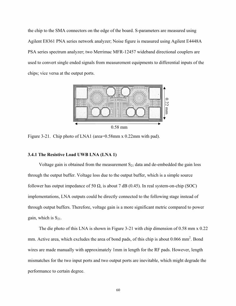
60
the chip to the SMA connectors on the edge of the board. S-parameters are measured using
Agilent E8361 PNA series network analyzer; Noise figure is measured using Agilent E4448A
PSA series spectrum analyzer; two Merrimac MFR-12457 wideband directional couplers are
used to convert single ended signals from measurement equipments to differential inputs of the
chips; vice versa at the output ports.
Figure 3-21. Chip photo of LNA1 (area=0.58mm x 0.22mm with pad).
3.4.1 The Resistive Load UWB LNA (LNA 1)
Voltage gain is obtained from the measurement S21 data and de-embedded the gain loss
through the output buffer. Voltage loss due to the output buffer, which is a simple source
follower has output impedance of 50 Ω, is about 7 dB (0.45). In real system-on-chip (SOC)
implementations, LNA outputs could be directly connected to the following stage instead of
through output buffers. Therefore, voltage gain is a more significant metric compared to power
gain, which is S21.
The die photo of this LNA is shown in Figure 3-21 with chip dimension of 0.58 mm x 0.22
mm. Active area, which excludes the area of bond pads, of this chip is about 0.066 mm2. Bond
wires are made manually with approximately 1mm in length for the RF pads. However, length
mismatches for the two input ports and two output ports are inevitable, which might degrade the
performance to certain degree.
0.22m
m
0.58 mm

61
Figure 3-22 to Figure 3-25 show measurement results of the LNA with simulation results.
Voltage gain is flat around 17 dB over wide bandwidth. The 3 dB bandwidth is from 0.2 GHz to
9 GHz. The measurement data has already subtracted the loss due to FR4 boards through
subtracting two measurement data of chip with board and board only.
Figure 3-22. Measurement (solid line) and simulation (dashed line) results of voltage gain for
LNA1.
Figure 3-23. Measurement (solid line) and simulation (dashed line) results of S11 for LNA1.
Figure 3-23 shows measurement results of reflection coefficients. It shows that S11 is lower
than -10 dB over very wideband. Measured results are better than simulated ones because the
directional couplers themselves are already matched to 50 Ω. Figure 3-24 shows the measured
0
5
10
15
20
25
Vol
tage
Gai
n(dB
)
0 1 2 3 4 5 6 7 8 9 10 Frequency (GHz)
-35
-30
-25
-20
-15
-10
-5
0
S11
(dB
)
0 1 2 3 4 5 6 7 8 9 10 Frequency (GHz)

62
reverse isolation and output return loss. The reverse isolation is better than 30 dB but has higher
value between frequencies from 6 GHz to 9 GHz. Since output is constructed as a source
follower stage, the output return loss is greater than 10 dB throughout all the frequencies.
Figure 3-24. Measurement results of S22 and S12 for LNA1.
Figure 3-25. Measurement (solid line) and simulation (dashed line) results of NF for LNA1.
Figure 3-25 shows the NF performance. Measurement results follow the trend of
simulation ones. NF has minimum value at 3 GHz of 4.2 dB, and it rises to 7.5 dB at 7.5 GHz
due to insufficiency in the gain of the amplifier.
0
2
4
6
8
10
12
0 1 2 3 4 5 6 7 8 9 10 Frequency (GHz)
NF
(dB
)
-60
-50
-40
-30
-20
-10
0
0 1 2 3 4 5 6 7 8 9 10 Frequency (GHz)
S12(
dB) &
S22
(dB
)
S22
S12

63
Note that the NF is measured with output buffer. It could be derived that the noise factor
related to output buffer is
13.0)(
14)(
42
12
1
==≈Lmbuffer
buffer
Lm
ombuffer
buffer
bufferM RgRg
RgF
buffer αγ
αγ
(3-14)
where rbuffer, αbuffer are the coefficients related to noise and rbuffer/αbuffer=1.33. If the noise
contribution of the output buffer is removed, the minimum NF of this LNA is actually 3.9 dB,
which is 0.4 dB improved compared to the measurement data.
Figure 3-26 shows the measured linearity results with both IIP3 and IIP2 which is
important for direct conversion receivers. Input third-order-intermodulation product (IIP3) is
about -8 dBm and IIP2 is better than 8 dBm. This LNA consumes about 20 mW of power
(excluding output buffers) with 1.2 V supply voltage.
Figure 3-26. Measured linearity results for LNA1.
3.4.2 The High Gain Wideband LNA (LNA 2)
The die photo of this LNA is shown in Figure 3-27 with chip dimension of 0.56 mm x 0.42
mm. Active area, which excludes the area of bonding pads, of this chip is about 0.134 mm2. This
-10
-5
0
5
10
15
0 2 4 6 8 10 Frequency (GHz)
IIP3
& II
P2 (d
Bm
)
IIP3
IIP2

64
LNA occupies greater chip area compared to LNA1 mainly because it uses two larger inductors.
Bond wires are made manually with approximately 1.5-2 mm in length for all the RF pads.
Figure 3-28 to Figure 3-32 show the measurement results of the LNA with simulation
results. From Figure 3-28, voltage gain is about 22.5 dB over wide bandwidth and starts to fall at
2.7 GHz. The 3 dB bandwidth is from 0.2GHz to 3.2 GHz. Figure 3-29 shows the measurement
results of reflection coefficients. It shows that S11 is lower than -10 dB over very wideband.
Figure 3-27. Chip photo of LNA2 (area=0.56mm x 0.42mm with pad).
Figure 3-28. Measurement (solid line) and simulation (dashed line) results of voltage gain for
LNA2.
Figure 3-30 shows the measurement results of the output return loss and the reverse
isolation. The output return loss is better than 20 dB across the whole bandwidth and the reverse
8
12
16
20
24
28
0 1 2 3 4 Frequency (GHz)
Vol
tage
Gai
n (d
B)
0.56 mm
0.42 mm

65
isolation is better than 30 dB. Figure 3-31 shows the NF performance. Measurement results
follow the trend of simulation ones. NF has minimum value at 3 GHz of 1.76dB. NF from 1 GHz
to 3 GHz is below 3 dB. This low NF and high gain makes this wideband LNA a good candidate
for multi-band receivers. The noise contribution of output buffer is about 0.03 (0.1 dB better)
according to equation (3-14). Output buffer has much smaller noise contribution compared to
LNA 1 because of the voltage gain is much bigger.
Figure 3-29. Measurement (solid line) and simulation (dashed line) results of S11 for LNA2.
Figure 3-30. Measurement results of S22 and S12 for LNA2.
Figure 3-32 shows the measured linearity results with both IIP3 and IIP2 which is
important for direct conversion receivers. Input third-order-intermodulation product (IIP3) is
-30
-25
-20
-15
-10
-5
0
0 1 2 3 4 Frequency (GHz)
S11
(dB
)
-70
-60
-50
-40
-30
-20
-10
0
0 1 2 3 4 Frequency (GHz)
S12
& S
22 (d
B)
S22
S12

66
about -9 dBm and IIP2 is better than 6 dBm. This LNA consumes about 25 mW of power
(excluding output buffers) with a 1.2 V supply voltage.
Figure 3-31. Measurement (solid line) and simulation (dashed line) results of NF for LNA2.
Figure 3-32. Measured linearity results for LNA2.
3.4.3 The Active Inductor Load UWB LNA (LNA 3)
Die photo of this LNA 3 is shown in Figure 3-33 with chip dimension of 0.38 mm x
0.36mm. Active area, which excludes the area of bond pads, of this chip is about 0.034 mm2.
Bond wires are made manually with approximately 1mm in length for the RF pads.
0
2
4
6
8
0 1 2 3 4 Frequency (GHz)
NF
(dB
)
-10 -8 -6 -4 -2 024 68 10
0 0.5 1 1.5 2 2.5 3 3.5 Frequency (GHz)
IIP3
& II
P2 (d
Bm
)
IIP3
IIP2

67
Figure 3-34 to Figure 3-38 show the measurement results of the LNA along with
simulation results. Figure 3-34 shows that the voltage gain is flat around 17 dB over wide
bandwidth. The 3 dB bandwidth is from 0.2 GHz to 9.2 GHz. The measurement data has already
subtracted the loss due to FR4 boards through subtracting two measurement data of chip with
board and board only. Figure 3-35 shows measurement results of reflection coefficients. It shows
that S11 is lower than -10 dB over very wideband. Measured results are better than simulated
ones because the directional couplers themselves are already matched to 50 Ω.
Figure 3-33 Chip photo of the LNA 3 (area=0.38mm x 0.36mm with pad).
Figure 3-34. Measurement (dotted line) and simulation (dashed line) results of voltage gain for
LNA3.
0
4
8
12
16
20
0 1 2 3 4 5 6 7 8 9 10 Frequency (GHz)
Vol
tage
Gai
n (d
B)
0.38mm
0.36mm

68
Figure 3-35. Measurement (dotted line) and simulation (dashed line) results of S11 for LNA3.
Figure 3-36 shows the measurement results of the output return loss and the reverse
isolation. The output return loss is better than 10 dB across the whole bandwidth and the reverse
isolation is better than 20 dB. Figure 3-37 shows the NF performance. Measurement results
follow the trend of simulation ones. NF has minimum value at 6.8 GHz of 3.4 dB.
Figure 3-36. Measured results of S12 and S22 for LNA3.
Figure 3-38 shows the measured linearity results with both IIP3 and IIP2 which is
important for direct conversion receivers. Input third-order-intermodulation product (IIP3) is
about -8 dBm and IIP2 is better than 8 dBm. This LNA consumes about 16 mW of power
-40
-30
-20
-10
0
0 1 2 3 4 5 6 7 8 9 10 Frequency (GHz)
S11
(dB
)
-60
-50
-40
-30
-20
-10
0
0 1 2 3 4 5 6 7 8 9 10 Frequency (GHz)
S12(
dB) &
S22
(dB
)
S12
S22

69
(excluding output buffers) with 1.2 V, 1.4 V, and 1.7 V supply voltages. However, most of the
current is flowing from 1.2 V power supply.
Figure 3-37. Measurement (dots) and simulation (dashed line) results of NF for LNA3.
Figure 3-38. Measured linearity results for LNA3.
3.5 Conclusions
In this study, design theory and considerations of proposed wideband LNA structure are
presented. The design employs capacitors and inductors along the feedback path, and
neutralization capacitors between input transistors. Packaging and ESD diodes are co-designed in
0
2
4
6
8
10
0 1 2 3 4 5 6 7 8 9 10
Frequency (GHz)
NF
(dB
)
IIP2
IIP3
-10 -8 -6 -4 -2 0 2 4 6 8
10 12
0 2 4 6 8 10 Frequency (GHz)
IIP3
& II
P2 (d
Bm
)

70
the simulation. Depending on the specification, gain, bandwidth, and NF are trade offs between
each other. Three LNAs were fabricated using pure digital CMOS 90 nm technology. These
LNAs achieve good performance in gain, bandwidth, and NF. Also they occupy small chip area
compared with other published LNAs. Table 3-1 summarizes the performance of the LNAs that
were fabricated in this study and their performances are compared with other published data.
Table 3-1. Measured performance compared with prior published works
CMOS Process
BW (GHz)
Voltage gain (dB) NF (dB) IIP3
(dBm)Package /ESD
Power (mW)
Vdd (V)
Area (mm2)
LNA 1 Dig. 90nm 0.2-9 17 4.2 min -8 y/y 20 (diff) 1.2 0.066
LNA 2 Dig. 90nm 0.2-3.2 22.5 1.76 min -9 y/y 25 (diff) 1.2 0.134
LNA 3 Dig. 90nm 0.2 - 8 17 3.4 min -9 y/y 16 (diff) 1.4 0.034
[20] Dig. 130nm 1-7 17 2.4 min -4.1 y/n 25 (diff) 1.4 0.019
[21] Dig. 90nm 0-6 17.4 2.5 min -6 n/y 9.8 1.2 0.0017
[22] 180nm 1.3-10.7 8.5 4.4 – 5.3 8 n/n 4.5 1.8 1
[22] 180nm 1.3-12.3 8.2 4.6 – 5.5 8 n/n 4.5 1.8 1
[19] RF 90nm 0.5-8.2 25 2.2 – 3.8 -4 n/n 42 2.7 0.025
[23] 180nm 1.2-11.9 9.7 4.5 – 5.1 -6.2 n/n 20 1.8 0.59
[24] Dig. 90nm 2-11 12 5.5 min -4 n/n 17 1.2 0.696
[25] 180nm 3.1-10.6 10.9 – 12 4.7 -10 n/n 10.57 1.5 0.665
[11] 180nm 2.3-9.2 9.3 4 - 8 -16 y/n 9 1.8 0.66
[26] 180nm 0.6-22 8.1 4.3 – 6.1 x n/n 52 1.3 1.35
[17] 130nm 3.1-10.6 15.3 2.04-2.98 <-5.1 y/y 9 1.2 0.87

71
CHAPTER 4 DESIGN OF WIDEBAND PASSIVE MIXERS
In this chapter, the behavior of resistive mixers is studied. The study begins with a board
level design of resistive mixers using Gallium Nitride (GaN) high electron mobility transistor
(HEMT) devices. Because of the inadequate modeling of GaN transistors operating in the linear
region, a linear model was developed and used in the design of resistive mixers. Three resistive
mixers were made with GaN transistors with different lengths and their results were compared
and examined.
After examining the performance of the GaN resistive mixers, focus is diverted to the
popular CMOS process for more integration of the circuit. First of all, a CMOS wideband
resistive mixer was made using the 0.18 µm CMOS technology. The resistive mixer covers a
wide frequency range up to 11 GHz. Next, a subharmonic pumped CMOS passive mixer with an
integrated VCO and a quadrature generation circuitry is examined at the end of the chapter. The
mixer has a better performance in the isolation between the LO to the output ports comparing to
the previous wideband mixer and can be used in low leakage applications, such as the
implementation of a frequency synthesizer discussed in Chapter 5.
4.1 GaN Passive Mixers
Wide bandgap semiconductor devices using GaN and SiC materials have drawn a lot of
attention recently. These devices have high breakdown voltages and therefore are suitable for
high power circuits. These high power circuits can be used in applications like satellite
communications, warfare systems, and cellular base stations. GaN-based devices have been
shown to have high power handling capability at microwave frequencies above X-band, and have
potential to generate high power at millimeter-wave frequencies as high as 100 GHz [27].

72
Several GaN circuits have been demonstrated, such as high speed switches [28], [29]; low
phase noise VCOs [30], [31]; power amplifiers [32]; and passive mixers [30], [33], [34]. The
previously reported GaN passive mixers had various conversion loss and linearity performances.
In order to examine the behavior of a GaN passive mixer, passive mixers were made in this
subsection.
Figure 4-1. Die photo of one of the GaN HEMT devices with a device area of 200 μm x 1 μm.
4.1.1 Modeling of GaN Transistors in the Linear Region
GaN HEMT transistors were provided by the Airforce. It provided devices with different
gate lengths and gate widths. Die photo of one of the GaN HEMT devices with a device area of
200 μm x 1 μm is shown in Figure 4-1. IC-CAP modeling software was used to obtain the
Curtice cubic model for the measured DC and AC performance and the parameters were further
optimized in Agilent Advanced Design System (ADS) simulator. However, from the simulation
results and the measurement data, some important mixer parameters can not be predicted well.
These parameters include the optimum gate bias voltage, and the LO power requirement for
achieving certain conversion loss performance. This is due to the fact that a resistive mixer is

73
operated in the linear region of a transistor and the Curtice model is mainly focused on the active
region. Therefore, efforts were made on the device modeling in the linear region.
Figure 4-2. Equivalent circuit model used for GaN HEMT devices.
In this work, accurate models in linear region at different gate bias voltages were created
based on measured data. The small-signal equivalent circuit model shown in Figure 4-2 was used.
Lg, Rg, Ld, Rd, Ls, and Rs are the parasitic components associated with the transistor interconnects
to the pads of three ports. Cp models the capacitance of the pads. Cds, Cdg, Cgs, and Rds are
transistor parameters that vary with the gate bias. Small-signal s-parameters were measured at
different gate biases with source grounded and drain biased at 0 V. The gate bias was varied
from -7 V to -2 V with 0.5 V step. The use of small-signal model reduces the complexity of
modeling and gives an accurate model in linear region, which is critical to the design of resistive
FET mixer.
Gate
Source
Cgd Rgd
Cgs
Rgs
Cds Rds Cp Cp
Ls
Rs
Cp
Drain Rg Lg
Cp
Ld Rd

74
The most important parameter that controls the conversion loss is the value of turn-on
resistance Rds. The behavior of Rds was curve-fitted using the sum of two hyperbolic tangent
functions with different weights:
)tanh()tanh( 22110 bgbgds VbVRVaVRRR ++++= (4-1)
,where R0, R1, R2, a, b, Vb1, Vb2 are constants and Vg is the gate bias. Two hyper-tangent terms
are used here because using only one term is not enough to fit the measured data very well. One
hyper-tangent term has a steeper slope whereas the other has a slower slope at the transition
region of Rds from turn-on to turn-off, which is critical for resistive mixer performance.
Figure 4-3. Modeled Rds versus gate bias on GaN devices with different gate lengths.
The model fitting results of Rds for the three GaN devices with different sizes of 300 μm x
0.75 μm, 300 μm x 1 μm, and 300 μm x 1.2 μm are shown in Figure 4-3. As shown in the figure,
the device with smallest gate length has the lowest value of turn-on resistance. The turn-on
-7 -6 -5 -4 -3 -2101
102
103
104
105
Gate Bias (V)
Rds
(Ohm
)
0.75um1.00um1.20um

75
resistances are 12.6 Ω, 15 Ω, and 23 Ω for gate lengths of 0.75 μm, 1.0 μm, and 1.2 μm,
respectively.
4.1.2 Design of GaN Resistive Mixers
The model of the transistors from the previous section was used in the Agilent Advanced
Design System (ADS) to simulate the conversion loss. The IF power was obtained using Fast
Fourier Transform of the transient data simulated by ADS. The simulation results of the
conversion loss versus LO power is shown in Figure 4-4 with comparison to measurement results
that will be discussed later.
Figure 4-4. Measured and simulated conversion loss versus LO power for GaN devices with different gate lengths.
The circuit was simulated with RF, LO and IF frequencies of 1.7 GHz, 1.9 GHz, and 200
MHz, respectively. The gates were biased at -5 V, -4.5 V and -4.7 V for the gate length of 0.75
μm, 1.0 μm, and 1.2 μm, respectively, where the lowest conversion loss for each circuit was
5 7.5 10 12.5 159
10
11
12
13
14
15
16
17
18
LO Power (dBm)
Con
vers
ion
Loss
(dB
)
mea 0.75ummea 1.00ummea 1.20umsim 0.75umsim 1.00umsim 1.20um

76
obtained. From the figure, it can be seen that the mixer using 0.75 μm device has the lowest
conversion loss since the turn-on channel resistance is the lowest among the three devices. The
figure also indicates that the conversion loss does not change much when LO power is increased
above 14 dBm, which matches pretty well with the measurement results.
Figure 4-5 shows the schematic of these single resistive mixers. LO is applied to the gate,
RF is applied to the drain, and the IF is generated at the source. Quarter wavelength transmission
lines are used in the RF and LO matching network as RF chokes. The open-circuited λ/4 line at
the IF end is used as LO and RF short to improve the LO-IF and RF-IF isolations.
Figure 4-5. Schematic of the single-FET resistive mixer.
4.1.3 Measurement Results
The circuits were fabricated on FR4 substrate with thickness of 1.6 mm. The dielectric
constant is 4.4 and the loss tangent is 0.022 at 2 GHz. Picture of one of the resistive GaN mixers
is shown in Figure 4-6. The three mixers were biased at their optimum bias points where the
minimum conversion losses were achieved. The optimum gate bias for devices with gate length
LO
RF
IF Gate Bias
λ/4 @ RF
GaN HEMT
LO Matching
RF Matching
Bond Wire
Bypass Cap

77
of 0.75 μm, 1 μm, and 1.2 μm were -5.2 V, -4.3 V, and -3.2 V, respectively. The bias voltage
were set to be just below the turn on voltage of each transistor, which allowed the LO signal to
turn on and off the channel effectively.
Figure 4-6. Photo of a GaN mixer board.
Figure 4-4 shows the measurement results of conversion loss versus LO power, in
comparison to the simulation results. For all the devices, the optimum LO power is 14 dBm. If
the LO swing is too small, the channel cannot turn on completely, therefore the conversion loss
will be higher. Simulated results are also shown in this graph. It matches pretty well for the
simulated data and measured data.
Figure 4-7 shows the frequency response of the conversion losses. It can be seen that all
three mixers have the lowest conversion loss at 1.7 GHz, where the mixers were designed for.
Figure 4-8 shows the conversion loss versus RF power, at RF=1.7 GHz and LO=1.9 GHz. The
LO power was fixed at 14 dBm. From the graph, we can see that the conversion loss of device
with the smallest gate length is the best among all. The conversion losses are 9.5 dB, 10.5 dB,

78
and 11.8 dB for devices with gate lengths of 0.75 μm, 1.0 μm, and 1.2 μm, respectively. The
input 1 dB compression points (P1dB) are 11 dBm, 11 dBm, and 12 dBm, respectively.
Figure 4-7. Measured conversion loss versus RF frequency.
Figure 4-8. Measured conversion loss versus RF power.
Figure 4-9 shows the two-tone third-order intercept point (IIP3) measurement results. The
figure shows both the fundamental and the 3rd order inter-modulation products with two-tone RF
-5 0 5 10 159
10
11
12
13
14
15
RF Power (dBm)
Con
vers
ion
Loss
(dB)
300um x 0.75um300um x 1.0um300um x 1.2um
1.55 1.6 1.65 1.7 1.75 1.8 1.85 1.98
9
10
11
12
13
14
15
RF Frequency (GHz)
Con
vers
ion
Loss
(dB)
300um x 0.75um300um x 1.0um300um x 1.2um

79
input at 1.7 GHz and 1.701 GHz. By extrapolating the measured data in the figure, IIP3 of 27
dBm, 25 dBm, and 24 dBm were obtained for the devices with gate length of 0.75 μm, 1 μm, and
1.2 μm, respectively.
Figure 4-9. Two-tone IIP3 measurement result of the GaN resistive mixers.
In conclusion, three GaN resistive mixers were designed, tested, and compared. The test
results show that these GaN resistive mixers have comparable performance to other mixers using
wide bandgap devices as well as GaAs HEMT devices. Table 4-1 shows the summary of the
performance of the mixers and Table 4-2 shows the comparison with other published results.
Table 4-1. Summary of the GaN resistive mixers
Gate Length (um)
CL (dB) P1dB (dBm)
IIP3 (dBm)
LO Power (dBm)
Gate Bias (V)
0.75 9.5 11 27 14 -5.2 1.0 10.5 11 25 14 -4.3 1.2 11.8 12 24 14 -3.2
0 5 10 15 20 25 30 -70
-60
-50
-40
-30
-20
-10
0
10
20
RF Power (dBm)
1st a
nd 3
rd O
rder
Out
puts
(dB
m)

80
Table 4-2. Summary of the III-V resistive mixers from existing publications
Technology Freq. (GHz) CL (dB) P1dB (dBm) IIP3 (dBm)
LO Power (dBm)
This work
AlGaN/GaN-HEMT 1.7 →0.2 9.5 10 26 14
[28] SiC-MESFET 5.175 →0.25 7.8 X 30 23
[28] AlGaN/GaN-HEMT 5.175 →0.25 7.3 X 36 30
[29] AlGaN/GaN-HEMT 12.4 →2.4 17 30 40 20
[30] SiC Diode 0.5 →0.1 12 x x x [35] InP MODFET 95.5 →1.5 9 8 x 8 [36] GaAs G-FET 5.2 →0.95 5.5 16 23 10 [36] GaAs D-FET 5.2 →0.95 7.4 4 13 0
4.2 CMOS Passive Mixer
In the previous section, the design of board level resistive mixer is shown. In this section, a
wideband resistive down-converting mixer was designed and fabricated using TSMC mixed-
mode 0.18 µm CMOS technology. Wideband matching at the RF ports and source follower at
output buffer at IF ports were used to achieve wideband frequency response. This resistive mixer
covers a wide frequency range from 1 GHz to 11 GHz with 7 ± 0.5 dB conversion loss. The
output buffer stage consumes 3 mW, which is much lower than previously published wideband
active mixers. This mixer is suitable for low power UWB devices.
4.2.1 Discussion on CMOS Resistive Ring Mixer
Techniques to derive the conversion loss of a passive mixer can be found in [37]. In order
to get the idea of how the bandwidth and conversion loss of the resistive mixers are determined,
three different CMOS technologies were used in the simulation to observe performances in the
frequency responses and conversion loss. The models used in this study are provided by TSMC.
Figure 4-10(a) shows the schematic of the simulated passive mixers using different gate
lengths and widths. Figure 4-10(b) shows the equivalent circuit while the mixer is operating and

81
this Figure will be discussed later. In the simulation, all of the transistors are provided with the
same power of LO signals at the gates.
Figure 4-10. Schematics of (a) a double-balanced CMOS resistive mixer, (b) an equivalent circuit of the resistive mixer.
Figure 4-11 shows the conversion loss of a double-balanced resistive mixer versus
frequency from 1 GHz to 20 GHz using three different CMOS technologies with gate lengths of
180 nm, 90 nm, and 65 nm. Four curves of conversion losses are shown in each graph with
different W/L ratios equal to 400, 300, 200, and 100. From Figure 4-11, several conclusions can
be made. First, for a certain technology, the smaller the ratio of W/L is, the higher the conversion
loss is. This is due to the turn-on resistor is smaller when the device is larger. Also, the smaller
W/L is, the conversion loss is more flat. Second, for different technologies, with the same W/L
ratio, the resistive mixer with smaller L has more flat conversion loss. Third, with the same W/L
ratio, devices with larger gate length have lower conversion loss.
CL
Rs
CL
Rs
Rs
Rt(t)
Rt(t-T/2)
Rt(t-T/2)
Rt(t)
LO Vrf
LO LO
LO
(a)
(b)
Cch(t-T/2)+Cj
Cch(t)+ Cj
Cch(t)+ Cch(t-T/2)+ 2Cj Cch(t)+ Cch(t-T/2)+ 2Cj
Cch(t)+ Cj
Cch(t-T/2)+Cj
Vrf Rs
Vrf
Vrf

82
The reason that the conversion loss is lower for larger length devices is that the turn-on
resistance is larger for deep submicron devices. When the gate length is getting smaller, the
electron mobility is also getting lower due to the high electric field at the gate as shown:
0
1 ( )effGS THV Vμμ
θ=
+ − (4-2)
, where effμ is the effective mobility, 0μ is the low field mobility, θ is a fitting parameter, VGS and
VTH are gate-source voltage and threshold voltage, respectively.θ is approximately inversely
proportional to the thickness of gate-oxide. Therefore, the short channel effect of the transistor
makes the mixer conversion loss higher.
Figure 4-11. Conversion loss versus frequency of CMOS resistive mixers with different gate lengths.
4.5
5.5
6.5
7.5
8.5
4.5
5.5
6.5
7.5
8.5
1 4 7 10 13 16 19 Frequency (GHz)
4.5
5.5
6.5
7.5
8.5
180nm
90nm
65nm
W/L = 400 W/L = 300W/L = 200W/L = 100
Con
vers
ion
Loss
(dB
)

83
The bandwidth dependency on the gate length could be described as follow. Determination
of the bandwidth can be seen from Figure 4-11(b). Rs is the source equivalent resistor from the
previous stage; Rt is the time-variant resistors of the transistors since they switch on and off
according to the LO signals, which has a period of T; CL is the load capacitance; Cch is the
channel capacitance of the transistors; and Cj is the junction capacitance of the transistors. For
transistors operating at different regions, channel capacitance varies according to the LO signal.
While the transistor is off, the channel capacitance is small (depletion capacitance) and while the
transistor is on (operated in linear region for a resistive mixer), the channel capacitance becomes
WLCox/2, where Cox is the oxide capacitance.
The bandwidth of the mixer is determined by the pole location located at the input of the
RF ports. The pole location can be seen as 1/RsCtot. Assume that the mixer is driven by an LO
signal with a square wave in the waveform shape, Rt(t) for one pair of the transistors is zero and
Rt(t-T/2) is infinity. If the passive mixer is divided into two half circuits since the double
balanced mixer is symmetrical in structure, the equivalent input capacitance is equal to
Ctot=2Cch(t)+2Cch(t-T/2)+4Cj. Since for CMOS transistors with a smaller gate length, under the
same W/L ratio, the channel capacitance as long as junction capacitance are smaller comparing
to transistors with larger gate length. As a result, the pole location of passive mixers with smaller
gate lengths is larger than the one with larger gate lengths.
In conclusion, resistive mixers with larger gate length will have narrower frequency
response, but will have lower conversion loss; on the other hand, resistive mixers with shorter
gate length will have wider bandwidth but will have higher conversion loss. Furthermore,
because transistors with smaller gate lengths have smaller capacitance comparing to transistors
with larger gate lengths, the bandwidth is also larger.

84
4.2.2 Design of CMOS Resistive Ring Mixer
A wideband passive mixer was designed using 180 nm CMOS technology. Figure 4-12
shows the schematic of the resistive ring mixer. Double balanced ring structure is used because
of the superior performance of the isolation between ports and the cancellation of the even-order
harmonics. At the RF input port, series inductors of 1.4 nH and shunt capacitors of 90 fF are
used for matching. In addition, shunt resistors of 250 Ω are used to improve the wideband
matching.
Figure 4-12. Schematic of the wideband resistive ring mixer.
No matching circuits are used at the LO port in order to reduce the circuit area. Without
the LO matching circuitry, the LO power needed to drive the resistive mixer to minimum
conversion loss is slightly higher, but the difference of 1- 1.5 dB in simulation is not significant.
In our simulation, LO power needed for the circuit is about 8 dBm to make the conversion loss
minimum.
RF
Vb
Vg
+
- Vdd
Vb
Vg
+
-
+ -LO
IF
Vdd

85
At the IF output port, source followers are used for impedance matching to 50 Ω, since the
lumped elements needed for 50 Ω impedance matching at 500 MHz IF would occupy too much
space on chip. Shunt capacitors to ground are used to make the LO and RF signals shorted to
ground and improve the LO-to-IF and RF-to-IF isolation. DC blocking capacitors are placed in
series to block DC biases of the source followers from the resistive mixer core.
Figure 4-13. Chip photo of the fabricated mixer (chip size including the pads: 0.95 mm x 0.65 mm).
Three DC biases for output buffer are supplied externally when measuring the circuit. The
optimum values for Vb, Vg, and Vdd are 0.5 V, 0.5 V, and 1 V, respectively. Increasing the value
of Vdd above 1 V does not make a significant difference on the mixer performance. Decreasing
the value of Vdd would increase the loss. Therefore, the lowest possible bias of 1 V is chosen to
lower the power consumption of the output buffer. The current flow through the source follower
is about 3 mA; therefore the power consumption is 3 mW. Figure 4-13 shows the die
IF IF-GND GNDGND
LO+
LO-
GND
GND
GND
GND
GND
GND
RF+
RF-
GNDVddVgVb

86
microphotograph of the resistive ring mixer. The size of the chip is measured 0.95 mm x 0.65
mm.
4.2.3 Simulation and Measurement Results
This mixer was measured on-wafer. Signal generators were used to generate the RF and
LO signals. Spectrum analyzer was used to measure the converted signal at the IF port. External
baluns were used at RF, LO, and IF ports. All the measurement losses from the baluns and the
cables were carefully calibrated using the network analyzer.
1 2 4 6 8 10 12
20
15
10
5
0 RF Frequency (GHz)
Con
vers
ion
Loss
(dB) Measurement
Simulation
Figure 4-14. Measurement and simulation results of conversion loss versus RF frequency with
fixed IF frequency 500 MHz.
Figure 4-14 shows the measured conversion loss from 1 GHz to 12 GHz. The solid line
with symbols indicates the measured data, whereas the dashed line indicates the simulated data
using CADENCE SPECTRE. LO frequency is 500 MHz higher than the corresponding RF
frequency, so that the IF frequency is fixed at 500 MHz. From the figure, the conversion loss is
within 7±0.5 dB from 1 GHz to 11 GHz, which covers the entire UWB band. The Vdd for the
bias circuitry is set at 1 V, and the current consumption is 3 mA. The total power consumption is

87
3 mW. The measurement results and simulation results are quite consistent with each other as
shown in the figure.
Figure 4-15 shows the measurement results for input 1 dB compression point (P1dB) and
input third-order intercept point (IIP3) for the CMOS wideband resistive ring mixer. It is well
known that resistive mixer has better linearity performance compared to the active mixers
because the transistors are operating in the linear region. For the linearity measurement, LO
power of 9dBm was applied to the resistive mixer. As shown in the figure, P1dB is 5±1 dBm for
1 GHz to 12 GHz. IIP3 was measured with two RF input signals separated by 10 MHz. Third-
order inter-modulation products were at 480 MHz and 520 MHz, where the first-order signals
were at 500 MHz and 510 MHz. As shown in the figure, IIP3 is within 9-13 dBm from 1 GHz to
12 GHz. This wideband mixer has very good linearity performance, which makes it suitable for
high dynamic range UWB receivers.
Figure 4-16 shows the measured performance of conversion loss versus LO power. In
resistive mixers, LO voltage swing has to be large enough to let the channel resistance of the
transistor reaches its lowest limit, so that the conversion loss could be minimized. However,
there is a limit of conversion loss where it will not improve any further with the increase of LO
power. The measurement was conducted at ten different frequencies from 1 GHz to 10 GHz,
with 1 GHz step. All the 10 curves in Figure 4-16 show the same trend that the higher the LO
power, the smaller the conversion loss. The conversion loss approaches to a limit when the LO
power is over 9 dBm, which is why 9 dBm of LO power was chosen in the previous
measurements. If higher conversion loss can be tolerated in some applications, the requirement
of LO power can be reduced. For example, for 10 dB conversion loss, LO power can be reduced

88
by half from 9 dBm to 6 dBm. Figure 4-16 also shows that the LO power requirement is almost
the same from 1 GHz to 10 GHz.
2 4 6 8 10 12-5
0
5
10
15
20
RF Frequency (GHz)
P1dB
and
IIP3
(dBm
)P1dBIIP3
Figure 4-15. Input P1dB and IIP3 versus RF frequency.
2 4 6 8 10
25
20
15
10
5
LO Power (dBm)
Con
vers
ion
Loss
(dB)
Figure 4-16. Measurement results of conversion loss versus LO power. The measurements were
conducted for ten RF frequencies from 1 GHz to 10 GHz.
Figure 4-17 shows the measurement result of S11 for the RF port from 100 MHz to 12 GHz.
The S11 was measured single-ended using GSGSG probe with one port terminated with 50 Ω.

89
The RF input matching is very wideband. The minimum return loss occurs at 3.5 GHz with 32
dB return loss. The overall return loss is better than 10 dB from 100 MHz to 6 GHz.
0 2 4 6 8 10 12-35
-30
-25
-20
-15
-10
-5
0
RF Frequency (GHz)
S11
(dB)
Figure 4-17. Measurement results of the RF return loss from 100 MHz to 12 GHz.
Figure 4-18. Measurement results of the NF of the wideband passive mixer.
Figure 4-18 shows the measurement result of the NF of the wideband passive mixer across
the frequency from 1 GHz to 10 GHz. The NF measurement was conducted using two different
LO power of 7 dBm and 10 dBm. The NF measurement was done at a fixed IF frequency of 500
0
2
4
6
8
10
12
14
16
0 2 4 6 8 10 12Frequency (GHz)
NF
(dB
)
0
2
4
6
8
10
12
14
16
0 2 4 6 8 10 12Frequency (GHz)
NF
(dB
)
LO=10dBm
LO=7dBm

90
MHz. While the LO signal is 7 dBm, the NF is around 11 dB and goes higher at frequencies
above 6 GHz. While the LO signal is 10 dBm, the minimum NF is 9.5 dB and also goes higher at
frequencies higher than 7 GHz.
In this mixer design, the double balanced structure was used in the resistive mixer to
improve the isolation. Across the whole band from 1 GHz to 11 GHz, the measured RF-to-LO
isolation is -39±1 dB, and LO-to-RF isolation is -37±1 dB. However, the isolation is not good
enough in certain applications such as the frequency synthesizer described in Chapter 5. With the
isolation, LO signal will leak to the output and cause spurious signals at the output. In order to
solve this problem, subharmonic mixer structure will be examined in the next section for the
improvements in the LO to output isolation.
4.3 CMOS Passive Harmonic Pumped Mixer
Subharmonic mixers draw a lot of attention recently in direct conversion receivers. One of
the biggest problem in implementing direct conversion receiver is that the feed-through of LO
signal might corrupt the receiving signal and saturate the gain stages along the receiving chain.
Also, subharmonic mixers become popular at millimeter wave where a low phase noise LO is not
readily available.
Traditionally mixers use fundamental LO signal and generate output frequencies of fout= fin
± fLO. As for subharmonic mixers, they use second, third, or even higher order harmonics of LO
signals to realize the frequency conversion. The output frequency of a subharmonic mixer is
LOinout nfff ±= (4-3)
, where n is the order of harmonic it uses.
To date, subharmonic mixers are published using all different kinds of materials, including
III-V compound semiconductors, SiGe, or HBTs. Recently CMOS mixers appear more and more

91
frequently on the research journals due to the ability of integration. In [38], double balanced
Gilbert cell subharmonic mixer was presented using BiCMOS process at PCS band. In [39],
performances of CMOS subharmonic mixers were analyzed in detail. In [40], transformer and
quadrature couplers were used as baluns and quadrature phase shifters in a CMOS Gilbert cell
subharmonic mixer. In [41], subharmonic CMOS mixers were exemplified even at millimeter-
wave frequencies using source-pumped LO or gate-pumped LO.
In this design, a ring structure passive subharmonic mixer is first demonstrated using a
1P6M 0.18 µm mixed-mode CMOS process with MIM capacitors and thick top metal for
inductors. A VCO is integrated with the subharmonic mixer. Quadrature phases of the VCO are
generated using divide-by-2 circuits. In section 4.3.1, schematics and system blocks are shown,
and in section 4.3.2, simulation and measurement results are provided.
Figure 4-19. Systematic blocks of the subharmonic mixer with an integrated VCO.
4.3.1 Discussions on Each Block
Figure 4-19 shows the block diagram of the passive subharmonic mixer with integrated LO
in this design. Four phases feeding into the subharmonic mixer are generated by a differential
VCO with a divide-by-2 circuit. For passive mixers, it is good to hard switch on and off on the
VCO
DIV-2
0o
LO Buffers
LO
RF
IF
Matching
Buffer 90o
180o
270o
RF Input
IF Output
Passive Subharmonic Mixer

92
gate of the transistors. Therefore, LO buffers are added to amplify the signals’ swing feeding into
the mixer.
A broadband matching circuitry is added at the RF input ports. Biasing is also applied from
the RF matching circuit. It is tricky for the RF and LO signals in a passive mixer so that optimum
conversion gain could be gotten. At the outputs, an output buffer is added for the measurement
purpose.
Figure 4-20. A 5 GHz VCO’s diagrams of (a) the schematic, and (b) the oscillation frequency.
Following shows the schematic and simulation results of individual blocks.
1. VCO and Divide-by-2 circuitry: Figure 4-20(a) shows the schematic of the 5 GHz VCO.
Configuration is a standard cross-coupled NMOS oscillator. The output is connected to
a divide-by-2 circuit through a RC level shifter. The inputs of a divide-by-2 circuit have
to be biased properly to get a more reliable dividing operation. Figure 4-20(b) shows the
simulated output frequency of the VCO. The VCO has output frequencies range from
Ib
Vdd
Vc
(a)
4.85
4.95
5.05
5.15
5.25
5.35
0 0.5 1 1.5 2Control Voltage (V)
(b)
Freq
uenc
y (G
Hz)

93
4.9 GHz to 5.3 GHz for the control voltage change from 0 V to 1.8 V. The tuning range
of the VCO is about 8% to the center frequency.
Divide-by-2 circuit is shown in Figure 4-21. Output of the VCO is first leveled
shifted through a RC level shifter, then feed into the divide-by-2 circuit. The divider is
implemented as cross-coupled current mode latches. Figure 4-22 shows the simulation
results of the signal feeding into the divider and the signal output from the divider. VCO
generates frequency of 5.1GHz and the divider successfully divides the input frequency
to one half.
Figure 4-21. Schematic of a current mode divide-by-2 circuit.
2. Mixer Core: Since resistive mixers mix incoming signals through the modulation of the
channel resistance of the transistors, it is worth to observe the variation in resistance of a
traditional resistive mixer and a resistive subharmonic mixer. Figure 4-23 and Figure 4-
24 show schematic and simulation results of the testing in variation in conductance of
Ib
Vdd
Ib
Vdd
Vin +
-
0o 180o 90o 270o
0o180o90o 270o

94
single NMOS transistor and a pair of NMOS transistors with differential gate-pumped
LO signals.
Figure 4-22. Simulation results of the divider input and output.
Figure 4-23. Variation of channel resistance of a (a) single NMOS with gate pumped LO, and a (b) parallel NMOS pair with differentially pumped LO.
The conductance of the channel resistance of a NMOS transistor is shown in Figure
4-24(a). The transistor is turned on every LO cycle of 400 MHz. The conductance of the
channel resistance of a pair of NMOS transistors is shown in Figure 4-24(b). The
differential LO signals alternatively turn on the transistors within the NMOS pair. This
is equivalent to using a LO signal which is two times the frequency using here. As a
IN
LO_0o
LO_180o
IN
LO_0o
(a) (b)
2.5
2.1
1.7
1.3
0.9
1.9
1.7
1.5
1.3
1.1 16n 17n 18n 19n 20n
Time (s)
Inpu
t (V
) O
utpu
t (V
)

95
result, this pair of the transistors could be used in substitute with the NMOS transistors
in the traditional resistive mixer.
Figure 4-24. Variation in conductance of a (a) resistive mixer, and a (b) resistive harmonic mixer.
Figure 4-25 shows the schematic of the proposed resistive harmonic double
balanced mixer. The structure is similar to the original resistive mixer, with single
NMOS becomes a parallel NMOS pairs. Gates of each transistor pairs are driven by the
LO signals with 180o phase difference. As a result, four phases are needed for a
harmonic balanced mixer.
Figure 4-26 and 4-27 show the transient simulation result and the correspondent
spectrum. Input signal is at 5.1 GHz and the VCO is oscillated at 5.35 GHz. The IF
output frequency is at 250 MHz. From the simulation result, the conversion loss of this
resistive subharmonic mixer is about 4 dB.
20m
16m 12m
8m 4m
0 0.0 10n 20n 30n
Time (s)
20m
16m
12m
8m
4m
0 Con
duct
ance
(mho
)
0.0 10n 20n 30n Time (s)
(a)
(b)
Con
duct
ance
(mho
)

96
Figure 4-25. Schematic of a resistive harmonic double balanced mixer.
Figure 4-26. Transient simulation of input and output.
3. RF biasing and matching: While the RF signals are fed into a subharmonic passive
mixer, they have to be biased properly so that the conversion loss can achieve optimal
performances. Figure 4-28 illustrates three different RF bias points, namely ①, ②, and
③, relatively to the four phases of LO signals. From ① to ③, the biasing points are
RF+
RF-
IF+
IF-
LO_0o
LO_180o
LO_0o
LO_180o
LO_90o LO_270o LO_90o LO_270o

97
moving higher toward the crossing points of four phases of the LO signals with a
voltage potential difference of ΔV. Figure 4-29 shows the simulation results of the RF
and IF signals of a subharmonic passive mixer with the three RF bias conditions
described in Figure 4-28. With bias condition ①, the RF signal is modulated by the IF
signal where the RF waveform has an envelope with frequency equal to the IF
frequency. Also can be seen from Figure 4-29(a), the IF signal is also modulated by the
RF signal. This is because that at a certain biasing point, transistors on different
branches in a sub-harmnic mixer (along the arrow shown in Figure 1) turn on at the
same time because the overlap in the waveforms of quadrature signals. Since the
transistors in each branch are in series to each other in a passive mixer, turning on two
transistors at the same time shorts the positive and negative nodes of the RF signal.
Similar analysis also applies to the IF signals.
Under the bias condition ③, the RF and IF signals do not interfere with each other
as shown in Figure 4-29(b). However, the magnitude of the IF signal is small (and thus
a higher conversion loss). This is because the transistors do not have enough of gate
voltage to be fully turned on completely. For a passive mixer, a large LO swing is
desired so that it can completely turn-on the switching transistors to achieve a good
mixing performance with less conversion loss.
The optimum biasing point would be the condition ② in Figure 4-28, where the
crossing points of the four phases LO signals are about a threshold voltage higher than
the RF biasing point. In this case, no short circuit would happen during the mixer
operation while the quadrature LOs turn on the transistors sequentially, and this pertain
the signal magnitude of the RF signal. However, the tradeoff would be the need of a

98
higher LO swing comparing to a fundamental passive ring mixer so that the transistors
still have enough of gate voltage to be fully turned on. In order to have a high LO swing,
inverters are used as buffers in this design to have a rail-to-rail LO swing. However,
steep edges after the inverters are not desired or that the LO crossing points shown in
Figure 4-28 would be too high. As a result, the buffers were intentionally designed to
have smaller sizes so that the LO waveforms can be smoother.
Figure 4-27. Output spectrums of the subharmonic mixer’s (a) input and (b) output.
Third, how to determine the sizes of the switching transistors? It is known that the
turn on resistance is smaller for bigger devices. The value required for turn on resistance
is set by the output frequency of the mixer. In this design, the output frequency is about
several hundred MHz. Because the frequency is not high, the device size could not be
that big. Device size of 20 µm/0.18 µm is chosen in this design.
RF @ 5.1GHz -17.24dBv
LSB -21.41dBv
(a) Input spectrum (b) Output spectrum

99
Figure 4-28. Different RF input biasing levels with differential LO signals.
Figure 4-29. Simulation results of the (a) RF waveforms, and (b) IF waveforms, of a subharmonic passive mixer with different RF bias conditions.
Time (ns) (a) (b) 10 8 6 4 2 0
-50
-30
10
30 50
-10
-50
-30
10
30
50
-10
Bias condition ①
Bias condition ②
Bias condition ③
0 3 6 9 12 15
-40
-20
0
20
40
Am
plitu
de (m
V)
-50
-30
10
30
50
-10
-40
-20
0
20
40
-40
-20
0
20
40
③
②
①
LO0o LO90o LO180o LO270o
ΔV

100
4.3.2 Measurement Results of the Resistive Harmonic Mixer
The proposed subharmonic passive mixer with an integrated quadrature LO was fabricated
using a 0.18 μm mixed-mode CMOS technology. The technology has six metal layers with a
thicker top metal layer for high-Q on chip inductors. Metal-insulator-metal (MIM) capacitors are
also provided in the technology. Die photo of the fabricated circuit is shown in Figure 4-30. The
chip has an area of 0.85 mm × 0.7 mm. External wideband baluns were used to convert
differential signals to single ended signals.
Figure 4-30. Die photo with an area of 0.85mm × 0.7mm.
The measured tuning frequency of the VCO is from 4.9 GHz to 5.3 GHz. The relationships
between the RF bias condition and the conversion loss are shown in Figure 4-31. As described in
the previous section, the conversion loss is minimal while the RF signal is biased at 1 V, which
would be about a threshold voltage lower than the crossing points of the four phases of LO.
Figure 4-32 shows the voltage conversion gain versus frequency. The gain de-embeds the loss

101
due to the output buffers and other measurement setups. In the measurement, the VCO is running
at a fixed frequency of 5 GHz (LO is running at half the frequency of the VCO). The RF signal is
swept from 3.5 to 7 GHz with the output IF frequencies varying accordingly. The lowest
conversion loss of -5.8 dB is achieved at 5.2 GHz. The mixer can be used from 3.5 GHz to 6.7
GHz within 3 dB gain variation.
-12
-10
-8
-6
-4
0.8 0.9 1 1.1 1.2RF Bias (V)
Con
vers
ion
Gai
n (d
B)
Figure 4-31. Effects of RF bias on the conversion loss of the mixer.
-12
-10
-8
-6
-4
-2
0
3.5 4 4.5 5 5.5 6 6.5 7
RF Frequency (GHz)
Con
vers
ion
Gai
n (d
B)
Figure 4-32. Measurement and simulation results of conversion gain of the mixer.

102
Figure 4-33 shows the measured LO power leakage to the RF and IF ports. The 1×LO
leakages to the RF port and IF port are about -35 dBm and -45 dBm across the LO tuning band;
and the 2×LO leakages are around -60 dBm and -65 dBm. Figure 4-34 shows the measured
linearity performance of the mixer. The 1 dB compression point is -10 dBm, the IIP3 is -2 dBm,
and the IIP2 is 26 dBm. The subharmonic passive mixer itself does not consume power, while
the power consumption of other components, including a VCO, divide-by-two circuits, LO
buffers, and IF buffers, is 25 mA under a 1.8 V supply voltage.
Figure 4-33. Measured LO leakage to the IF and RF ports with varying LO frequency.
4.4 Conclusions
In this chapter, several kinds of resistive mixers with different topologies and fabrication
topologies are presented. First, a board level GaN resistive mixer is discussed in detail with
modeling and mixer performance. Next, a 0.18 µm CMOS resistive ring mixer on TSMC mixed-
mode technology was designed, fabricated, and measured. The resistive ring mixer has very wide
bandwidth covering from 1GHz to 11GHz with 7±0.5 dB conversion loss. Finally, a
subharmonic CMOS resistive mixer is also measured. The subharmonic mixer is suitable for
-80 -70
-60 -50 -40 -30 -20 -10
0
2.45 2.5 2.55 2.6 2.65 LO Frequency (GHz)
Leak
age
Pow
er (d
Bm
)
LO-RF LeakageLO-IF Leakage 2LO-RF Leakage 2LO-RF Leakage

103
direct conversion receiver because of its immunity to LO feed through problem. The
subharmonic mixer will be used in the OFDM-UWB frequency synthesizer in Chapter 5. It helps
the frequency synthesizer to have smaller LO leakage at the output. The two CMOS passive
mixers are summarized in Table 4-3.
-30 -20 -10 0 10 20 30
-100
-80
-60
-40
-20
0
20
40
Input Power (dBm)
Out
put P
ower
(dBm
)
Figure 4-34. Measured P1dB, IIP2, and IIP3 of the passive subharmonic mixer.
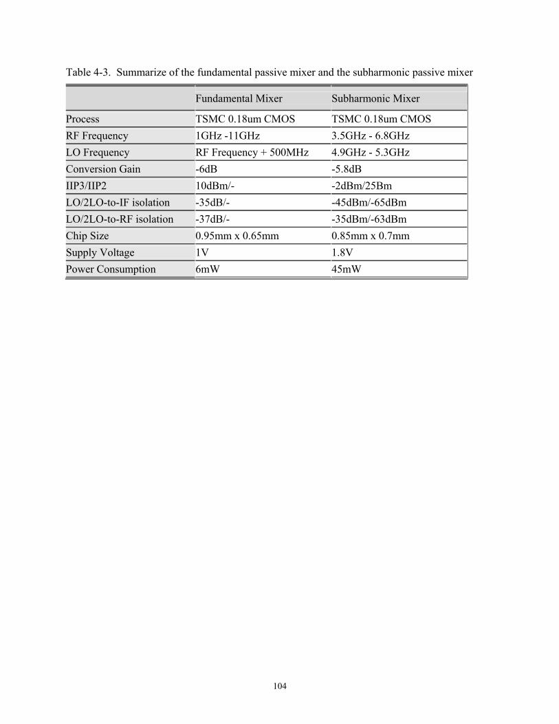
104
Table 4-3. Summarize of the fundamental passive mixer and the subharmonic passive mixer
Fundamental Mixer Subharmonic Mixer
Process TSMC 0.18um CMOS TSMC 0.18um CMOS
RF Frequency 1GHz -11GHz 3.5GHz - 6.8GHz
LO Frequency RF Frequency + 500MHz 4.9GHz - 5.3GHz
Conversion Gain -6dB -5.8dB
IIP3/IIP2 10dBm/- -2dBm/25Bm
LO/2LO-to-IF isolation -35dB/- -45dBm/-65dBm
LO/2LO-to-RF isolation -37dB/- -35dBm/-63dBm
Chip Size 0.95mm x 0.65mm 0.85mm x 0.7mm
Supply Voltage 1V 1.8V
Power Consumption 6mW 45mW

105
CHAPTER 5 CONSIDERATION AND DESIGN OF AN UWB FREQUENCY SYNTHESIZER
At the beginning of this chapter, a switching band VCO was designed and tested. The
design considerations about a switching band VCO are also provided. This switching band VCO
has a tuning range from 3 GHz to 4.3 GHz.
Although the tuning range of the switching band VCO is large, it still lacks the ability to
tune the whole UWB spectrum from 3 GHz to 10 GHz. Furthermore, because of the special
requirements on the wide frequency covering range and the ultra fast switch time, traditional
PLLs could not be used in this design. As a result, a frequency synthesizer based on single-side-
band (SSB) mixers with only one VCO used for a MB-OFDM UWB system was designed and
simulated.
The structure of Chapter 5 is listed as follows. Section 5.1 describes a switching multi-
band VCO. Brief introduction to the frequency synthesizer is given in Section 5.2; topology that
is used in this study is presented in Section 5.3; concerns about spurious signals are given in
Section 5.4; finally simulation results of the CMOS implementation of the ideas are shown in
Section 5.5.
5.1 A Switching Band VCO
Voltage controlled oscillators (VCOs) usually utilize the change in capacitance value of
varactors to make the frequency tuning. However, the capacitance variation of capacitance in
varactors is limited if a wideband VCO is needed. There are several reasons why the VCOs with
wideband tuning range are wanted. First of all, because of the reduction of the supply voltage in
sub-micron CMOS technology, the voltage variation that is used on varactors also reduces. This
limits the variation in capacitance of varactors. Second, multi-band transceivers are getting
popular since engineers are trying to design universal transceiver, which could be used in

106
conjunction with a fast adaptive signal processing chip and adaptively modified the configuration
to fit different communication standards. In this case, the VCO has to run at frequencies covering
the whole bands. Third, because of process variation, running frequency of a VCO will be
different from wafer to wafer. In order to increase the yield so to reduce the cost of making the
chips, extensive calibration techniques are employed on modern CMOS communication chips.
People in [42] use extensive varactor bands and digitally control the capacitance in the resonant
tank to cope with the variation in the temperature, process, and voltage.
In order to design a VCO with wide tuning frequency range, concept of switching resonant
tank is proposed in [43], [44], and [45]. Either inductor or capacitor could be switched to change
the resonance frequency of the tank. However, papers presented so far do not have the ability to
switch both of the inductors and the capacitor. In this design, a switching band VCO was
designed to show the ability of the switching resonant using both switching inductors and
switching capacitors. Design considerations will be provided in Section 5.1.1; experiment results
will be provided in Section 5.1.2.
5.1.1 Design of the Switching Band VCO
In order to change running frequencies using switching resonant tanks, two components
could be used to switch, one is capacitor, and the other one is inductor. Switching capacitors is
desired as the first thought because the area occupied of inductors is usually big and makes the
chip huge and costly. In order for an oscillator to start oscillate, the criteria
Gmω2L2/Rs=GmQind2Rs>1 should be fulfilled, where Gm is the effective transconductance of the
VCO core transistor, ω is the oscillation radian frequency, L is the inductance value in the
resonant tank, Rs is the equivalent series resistance of the inductor, and Qind is the Q-factor of the
inductor. In general, Q factor of inductors are roughly on the same order for certain technology.
In order to maintain power consumption (Gm) to some acceptable value, Rs has to be increased.

107
From equation Qind=ωL/Rs, it can be seen that inductance value has to be larger while Rs is
increased. For a VCO with extreme wide tuning range, e.g. highest frequency to lowest
frequency ratio of 1.5, keeping inductance value the same might not be a good choice. For an
oscillator, small inductor in the resonant might cause the oscillator failing oscillate due to
insufficiency in feedback gain. While a switching oscillator is running at low frequency mode,
inductor value should be increased compared to the high frequency mode. Therefore, switching
inductor is desired while the tuning range is extremely wide.
Figure 5-1. Schematic of the switching band VCO.
However, too many switching inductors would make chip size too large. Two switching
inductors are used in this design. Three levels of tuning mechanism are used in this VCO from
coarse tuning to fine tuning. Switching inductor set the first level of tuning frequency. Two bits
VL Tuning Tank
Vc
VC1 VC2 VC2 VC1
LbLb L1 L1
L2L2 ML ML
Mb Mb
Mi
M1 M2
C1 C1C2C2
Cv Cv
Mc1 Mc2 Mc2 Mc1

108
of switching capacitors are used as second level of tuning frequency. Finally, varactors are used
as the third level of tuning frequency, and they make the output frequencies of the VCO
continuous throughout the spectrum. As a result, there are totally eight different frequency
settings for this switching band VCO.
Figure 5-1 shows the schematic of this switching band VCO. M1 and M2 form the PMOS
cross coupled pair to provide feedback for oscillation. Mi provides the bias current. L1s and L2s
are resonant inductors. L2s could be switched on and off using switches ML. C1s, C2s, and Cvs
form the resonant capacitance. Both of C1 and C2 could be switched on and off using transistors
Mc1 and Mc2.
Leeson-Cutler’s Formula is presented as
)1]()2
(1[2log10)(3/120
ω
ω
ωωω
Δ
Δ+
Δ+=Δ f
Ls QPkTFL (5-1)
,where k is Boltzmann's constant, T is the absolute temperature, F is noise factor of the core
transistors, Ps is the average power dissipated in the oscillation tank, w0 is the oscillation
frequency, QL is the total quality factor of the tank, Δω is the offset from the carrier, and Δω1/f3
is the corner frequency between the 1/f3 and 1/f2 regions. From the formula, it could be seen that
phase noise of an oscillator is controlled by the Q factor of the resonant tank for certain
technology and power of the signal. Figure 5-2 shows the equivalent circuits of switching
inductors while the switch is on or off. For switching band VCOs, in order to make the phase
noise stays constant for all bands, Q have to be the same whether switches are on or off. While
the switch is off, the Q factor is
1
2
1
2
21
2
21
21
21
21
)1()()(
LL
QLL
RRLL
RRLLQoff
+
+=
++
=++
=ωω (5-2)

109
While the switch is on, the Q factor is
11
1
1
1 QRL
RRLQ
ONon =≅
+=
ωω (5-3)
where Q1 and Q2 are the Q factors for inductors L1 and L2. Ron is the turn on resistor of the
switch. The approximation in equation (5-3) is while Ron is much smaller then the series
resistance of inductor L1. This means the transistor size has to be large enough to make the turn
on resistor almost negligible compared to the series resistance of the inductor. Make equation (5-
2) and (5-3) equal will lead to Q1=Q2. As a result, Q factor of the two inductors has to be
designed equally so that the phase noise would be kept the same for all the switching bands.
Figure 5-2. Schematic of resonant tank when (a) low frequency mode, and (b) high frequency
mode.
The two capacitors in the capacitor bank are designed to have capacitance ratio of two to
one. In this case, the total capacitance value could be varied from three unit capacitance to zero
unit capacitance. Also, the Q factors of capacitors in the resonant tank should be kept constant
for all switching bands. Q factor of a capacitor is defined as Qc=Rcs/ωC, where Rcs is the series
resistance to the capacitor. To keep Qc the same, Rcs has to be changed according to the value of
L1
L2
R2
R1
C
RON
VL=0V VL=1.8V
L1
L2
R2
R1
C
(a) (b)

110
capacitance C. Therefore, the size of switching transistors control the capacitors should be scaled
in proportional to the value of capacitors.
The switching band VCO is designed and fabricated using TSMC 0.18 μm CMOS mixed-
mode technology. The technology has six metal layers with top metal layer of 2μm thickness for
high-Q inductors. The inductors used here have octave shape to increase the Q value compared
to square inductors. Values of two inductors are 0.46 nH and 0.31 nH. Q factors of these
inductors are 10 at 5 GHz. The small values of inductors are used for intention to have wider
tuning range. The two capacitors are implemented in MIM capacitors with values of 850 fF and
430 fF. All of the NMOS switches are made large so that the turn on resistor is small to reduce
the Q factor of the resonant tank. For the switching inductor, the switch size is 600μm/0.18 μm.
For the switching capacitors, switches have size of 600 μm/0.18 μm and 300μm/0.18 μm for the
larger capacitor and the smaller capacitor, respectively. The output buffers use large inductors to
drive external 50 Ω equipments.
Figure 5-3. Die photo of the switching band VCO.
5.1.2 Experimental Results
Figure 5-3 shows the die photo of the proposed VCO. The chip has size of 730 μm in

111
length and 660 μm in width. Measurements are done with GSGSG probes, and phase noise is
measured using HP/Agilent 70420A baseband phase noise test set. The three control bits are set
externally. 1.8V supply voltage is used with about 11mA current flowing through the core VCO.
Figure 5-4. Measured conversion loss versus offset frequency.
While VL is set to 1.8 V, VCO is operating in low band; while VL is set to 0 V, VCO is
operating in high band. Each of the bands could be subdivided into four sub-bands that are
controlled by switching on and off capacitors. In each of these two bands, two capacitors are
switched on and off using Vc1 and Vc2. Varactors are tuned from 0 V to 1.8 V. For low band,
-140
-120
-100
-80
-60
-40
-20
0
1E+03 1E+04 1E+05 1E+06
-140
-120
-100
-80
-60
-40
-20
0
-140
-120
-100
-80
-60
-40
-20
0
-140
-120
-100
-80
-60
-40
-20
0
101 001
Offset Frequency (Hz) 1E+03 1E+04 1E+05 1E+06
Phas
e N
ois
e (d
Bc/
Hz)
110 010
000
011111
100

112
frequency of the VCO could be tuned from 2.89 GHz to 3.45 GHz, which is about 17.7 % of
tuning range; for high band, frequency of the VCO could be tuned from 3.59 GHz to 4.3 GHz,
which is about 18 % of tuning range. The operating frequencies of the VCO are about 7 % lower
compared to simulation ones due to the error in estimating capacitances of traces. Also, some
pieces of traces attribute certain amount of inductance are not considered when doing the
simulation.
Figure 5-5. The tuning capability of the switching band VCO.
Measured phase noise is about -110 dBc/Hz at 1 MHz away from the oscillating frequency.
For the highest two bands, the phase noise drops to about -105 dBc/Hz at 1MHz separation.
Measurement phase noise results are about 5 dB worse than the simulation ones also due to metal
parasitics in the layout.
Graphs of measured phase noise are shown in Figure 5-4. Eight plots are presented for
each of the sub-bands. Figure 5-5 illustrates the tuning frequency range of each different control
settings. Four sub-bands in low band have frequencies covering each other a little bit and same
as the four sub-bands in high band.
In summary, an eight-band digitally controlled band-switching VCO using 0.18 μm CMOS
2.5
2.7
2.9
3.1
3.3
3.5
3.7
3.9
4.1
4.3
4.5
Fre
quen
cy (
GH
z)
110 010 100
000
111011
101 001
VC1VC2VL

113
technology is demonstrated. Design methodology is described. The measurement results show
that the VCO covers two bands of 2.9 - 3.45 GHz and 3.6 - 4.3 GHz. Phase noise of the VCO
stays constant around -110 dBc/Hz at 1 MHz offset across all bands. Table 5-1 summarizes the
performance of this band-switching VCO.
Table 5-1. Performance summary of the band switching VCO
`
5.2 Introduction to MB-OFDM UWB Frequency Synthesizers
Due to the requirement of high data rate wireless transmissions, large spectrum bandwidth
was released for this purpose. Because of the extremely crowded spectrum usage at lower GHz
frequencies, FCC released 3-10 GHz spectrum for the use of ultra-wideband (UWB) applications.
Couples of different groups are working on setting up standards for use of this wide spectrum.
Two standards occupy most of the markets now. One of which is based on the pulse-wave
transmission, which transmit ultra short pulses (ultra-wide bandwidth) as digital signals. These
kinds of systems were used in sensor applications or radar applications for military purposes.
The other group of people is trying to modify the existing mature standards people use on
wireless communication and fit them into ultra-wideband systems so that the developing time
DC1DC2DL* Freq (GHz) Tuning
Range (%) PN@100KHz (dBc/Hz)
PN@1MHz (dBc/Hz)
110 2.89-3.08 6.4 -88.31 -108.98 010 2.97-3.18 6.83 -88.04 -111.36 100 3.01-3.22 6.7 -86.71 -108.29 000 3.19-3.45 7.8 -89.34 -111.75 111 3.59-3.86 7.13 -88.35 -110.24 011 3.68-3.97 7.58 -83.54 -111.27 101 3.83-4.14 7.78 -73.74 -105.51 001 3.93-4.3 8.99 -85.31 -106.23
*C1 is on/off for DC1=1/0; C2 is on/off for DC2=1/0; L is on/off for DL=0/1

114
might be shorter. One of the most important standards come out is the use of multi-band OFDM
signals [46]. This alliance adapted the mature OFDM technology that is used in IEEE 802.11a
and 802.11g. First of all, the whole ultra-wideband is divided into several narrower bands, and
each narrow band signals are transmitted using the OFDM modulation. The transmission data
rate of this specification is ranged from 53 Mbps to 480 Mbps depends on the coding schemes
and operating distances.
Table 5-2. Center frequencies plan for OFDM UWB
Band Group 1 2 3 4 5
BAND_ID 1 2 3 4 5 6 7 8 9 10 11 12 13 14
Center Freq (MHz) 3432 3960 4488 5016 5544 6072 6600 7128 7656 8184 8712 9240 9768 10296
Figure 5-6. Frequency plan chart of the OFDM UWB.
The whole 3-10 GHz band is divided into 14 sub-bands. Each sub-band has bandwidth of
528 MHz. Table 5-2 lists all the central frequencies of each of sub-bands and Figure 5-6
illustrates the frequency planning of this OFDM UWB system. The 14 sub-bands are categorized
into five groups. Band group 1 is mandatory when developing MB-OFDM devices and other
four band groups are optional. The use of those four bands is reserved for future use and it has
more flexibility when designing the devices. Most of the developments in this system today are

115
major focused on band group 1 because at lower frequencies chips could be made on mature and
cheap CMOS technology. Switching between the frequency bands is controlled by the time
frequency coding. The time frequency coding provides frequency diversity gain and robustness
to interferences.
The maximum distances at which the multi-band OFDM system can achieve package error
rate of 8 % for a 90 % link success probability are listed in Table 5-3. The testing was done
under different channels from all white Gaussian Channel (AWGN) to channels with large delay
spread. The operating distances are in the range of 10 meters, which is far enough for short range
high data rate transmission systems such as the linking the DVD player to a digital television.
Table 5-3. Operating distances for OFDM UWB system with different channel conditions and date rate
Range AWGN LOS : 0-4m CM1
NLOS : 0-4m CM2
NLOS : 4-10m CM3
RMS delay spread : 25ns CM4
110 Mbps 21.4m 12.0m 12.0m 11.5m 10.9m 200 Mbps 14.6m 7.4m 7.1m 7.5m 6.6m 480 Mbps 9.3m 3.2m 3.0m N/A N/A
Figure 5-7 illustrates timing diagram of band switching operations between the different
sub-bands of an MB-OFDM UWB system. It is noticed that the guard interval, which also equals
the transition time between bands to bands, has only a period of 9.5 ns. There are several ways to
achieve frequency hopping for a frequency synthesizer at this kind of speed. First is the use of
ultra fast settling time phase-lock-loops (PLLs). The second method is to use multiple PLLs and
select outputs from different PLLs when the center frequency has to be changed. Third, using up-
conversion mixers, down conversion mixers, and switches in combination to make the selection

116
of frequencies fast. A briefing on how the previous designs were done for such a frequency
synthesizer will be given in the following sections.
Figure 5-7. Frequency hopping diagram between the different bands.
5.2.1 PLL with an Ultra Fast Settling Time
PLL is usually implemented as a frequency synthesizer in a communication system
because of its capability to generate a stable output frequency. Since the 528 MHz frequency
resolution in MB-OFDM UWB systems is pretty wide, the use of integral-N frequency
synthesizers would suffice.
Figure 5-8. Block diagram of an integral-N frequency synthesizer.
Figure 5-8 shows the block diagrams of an integral-N frequency synthesizer. Basic
operation of an integral-N frequency synthesizer could be briefly described as follows. The
PFD Loop Filter
Divider
VCO

117
divider divides the frequency of VCO output signal N times and compares its phase with the
input reference clock in phase frequency detector (PFD). PFD generates pulses if there are phase
differences between the two signals. Pulses from PFD are filtered through a low pass loop filter
and generates a control signal which the magnitude is determined by the amount of phase
difference. The control signal then controls the output frequency of the VCO. Phases of signals
after the divider and the input reference clock would be locked through negative feedback, and
this also guarantees the output signal frequency would be exactly equal to N times the frequency
of the input reference signal.
Figure 5-9. Block diagram with mathematical modeling of integral-N PLL.
Figure 5-9 shows the block diagram of an integral-N PLL with frequency domain model of
each block [47]. For a second order, type-II frequency synthesizer, the frequency domain transfer
function is:
p
z
wsws
sCsH
/1/11)(
++
= (5-4)
, where C is determined by the values of the capacitors in the loop filter and wz and wp are zero
and pole frequencies in the transfer function.
The open loop gain is
π1
VCO
Icp H(f)jfkv
N1
Loop Filter
Charge PumpPFD
outφinφ
Divider
+
-

118
NssHIK
sA cpv
π)(
)( = (5-5)
,and the closed loop gain is
)(1)()(sA
sAsGin
out
+==
φφ
(5-6)
Figure 5-10. Settling behaviors of (a) a step response, and (b) closed loop frequency response, of a fast switching PLL.
Settling behavior and stability analysis could be got from these equations. Figure 5-10
shows the closed loop step response and the closed loop frequency response. These graphs were
generated using PLL Design Assistant software by Michael Perrott from MIT. This PLL has
settling time about 10 ns. However, the cutoff frequency which determines the 3 dB roll off point
in the frequency response is at 500 MHz. Reference frequency is typically about 10 times higher
than the cutoff frequency and it will lead the reference frequency as high as 5 GHz. The
implementation with a reference signal running at 5 GHz would usually consume a lot of power
on CMOS chips and make this solution unattractive since the phase detector and charge pump
(b) (a)

119
circuits would not work very well at this high frequency unless they draw huge current. Also,
from Section 5-1, it can be seen that it is extremely difficult to have a VCO running through all
the UWB bandwidth. Therefore, the traditional integral-N PLL methodology is out of
consideration while designing UWB frequency synthesizers.
5.2.2 Switching Between Multiple PLLs
Figure 5-11. A MB-OFDM UWB frequency synthesizer using multiple PLLs in [48].
Since the traditional PLLs are not fast enough to satisfy the timing requirement of MB-
OFDM UWB system as shown in the previous section, one of the straight forward way is to use
several PLLs running at different frequencies and select from them using the switches in a
frequency synthesizer. For example, if three frequency bands are required, three PLLs will be
implemented and switched between each other in a frequency synthesizer according to digital
control signals. In [48], Razavi etc. presented a three-band MB-OFDM UWB frequency
synthesizer. Figure 5-11 shows the block diagram of the implementation. Three PLLs are shown
in the block diagram. Selecting time between them is fast enough to satisfy the requirement of
the specification. This design only generates the three frequencies in group 1 bands. If more

120
frequency bands have to be implemented in the design, then more than three PLLs have to be put
on the same chip. In the standard, 14 bands are spreads over 3- to 10-GHz. Using this
architecture, 14 PLLs have to be implemented, which is unrealistic and the whole chip area will
be bulky and consumes a lot of power.
Figure 5-12. A MB-OFDM UWB frequency synthesizer using two swapping PLLs. Illustrations of (a) timing diagram, and (b) simplified block diagram, in [49].
A smart way to reduce the number of PLLs is to effectively utilize the time between each
symbol for PLL to reach its steady condition. Figure 5-12 [49] illustrates one of the
implementations of this idea. The transition of two switching bands is 9.5 ns, which is too short
for a PLL to response. However, the symbol period of 312.5 ns is long enough for a PLL to
stabilize. Two PLLs are used alternatively in this synthesizer. While one PLL is set to a certain
frequency, the other PLL has already started to tune to the next frequency. Therefore, the settling
time is relaxed from 9.5 ns to about 320 ns which greatly reduce the speed requirements of a
PLL with the use of one extra PLL.
(a) (b)

121
5.2.3 Switching Between Different Frequencies Using Mixers
The most popular scheme used in the designing of UWB frequency synthesizers is to use
mixers to switch between different bands. Since mixers are not used in feedback systems like
PLLs, the settling time only depends on the loading capacitances and the currents to charge them.
A useful architecture is the use of single-side-band (SSB) mixers that can generate two bands,
one of up-side band and one of lower-side band. As a result, mixers are extensively used in the
multi-band OFDM UWB frequency synthesizers. Figure 5-13 illustrates two of the
implementations from [50] and [51] using mixers in frequency synthesizers. Through careful
frequency planning and proper design, only one PLL is necessary in the frequency synthesizer.
In [51], several different frequency plans using this kind of technique are proposed, and the
publication gives us an idea of the trade-offs between different schematics.
Figure 5-13. Two implementation of MB-OFDM UWB frequency synthesizers in (a) [50], and in (b) [51].
5.3 The Proposed OFDM UWB Frequency Synthesizer
The main problem in using single-side-band mixers in a frequency synthesizer is the
spurious tones generated from the mixers. While using a PLL, the spectrum of the output signal
is a pure sinusoidal wave. However, signals from a mixer suffer from the nonlinearities of the
(a) (b)

122
mixer itself. The output signal will not be a clean sinusoidal signal but a signal with large
harmonic terms and intermodulation terms. Spurious signals in a frequency synthesizer would
degrade bit error rate (BER) performance comparing to pure sinusoidal waves.
Under most conditions, spurious signals are far away from the target frequencies and they
could be easily filtered out. However, in MB-OFDM UWB frequency synthesizers, filters with
very wide tuning range have to be designed since the whole frequency span is 7 GHz wide. A lot
of filters might necessary be implemented either on chip or off chip. Therefore, the most serious
problem about designing a MB-OFDM UWB frequency synthesizer is to clean the output
spectrum.
5.3.1 Effect of Spurious Signals in Frequency Synthesizers on BER performance
In order to get the ideas of how spurious signals affect BER performance of a MB-OFDM
UWB system, simulation is performed in Agilent Advanced Design System (ADS). Figure 5-14
illustrates the diagram of spurious signals generated from a frequency synthesizer. Signal at f0 is
the desired LO frequency; signals at fu and fl are the upper-side band spurious signal and lower-
side band spurious signal which are mainly generated due to the nonlinearity of mixers. The
desired frequency has signal amplitude of 0 dB, which is a reference to the spurious signals and
the spurious signals have the signal amplitude of –A dB.
Figure 5-14. Spurious signals of a frequency synthesizer.
0dB
-A dB-A dB
f0 fu fl

123
Figure 5-15 shows the simulation block diagram of the effect on BER due to spurious
signals in a MB-OFDM UWB system. In this simulation, direct conversion receiver is assumed
since this architecture is easier to be integrated on a single chip without many external
components. UWB OFDM function blocks generate OFDM signals through IFFT, and then the
signals are up-converted to the RF frequency using spurious contaminated LO signals. In this
simulation, three transmitters are added together to represent the input signal to the receiver. The
transmitter in the center represents the desired signal with LO at frequency f0, and the other two
transmitters represent interference signals due to spurious tones from LO at frequency fh and fl.
Spurious signals have following gain stages of –A dB. At the receiving end, input signals with
interferences are down-converted to baseband through a down-converting mixer and a LO at
frequency f0. Baseband signal is further processed by FFT and the data are recovered. BER
detector detects the error due the interferences made by spurious tones in the frequency
synthesizer.
Figure 5-15. Simulation diagram of effect on BER due to spurious signals in a frequency synthesizer.
UWB OFDM
LOspu1
-A
UWB OFDM
LO
1
UWB OFDM
LOspu2
-A
UWB OFDM Receiver
LO
BER Detector
TX RX

124
Figure 5-16 shows the simulation results of BER performance versus signal to noise ratio
with different signal levels of spurious tones in the frequency synthesizer. BER degradations due
to the spurious signals are compared with the perfect OFDM system. It can be shown while
interference gets larger, BER degrades more as expected. Assume that only 1db degradation in
BER is acceptable due to interference tones so that the whole system performance does not
change a lot. This figure indicates that at least 25 dB of suppression to the desired signal on
spurious signal is necessary.
Figure 5-16. Simulation result of BER with various spurious signal levels.
However, the scheme in the simulation above is optimistic. In a communication system,
usually the interference’s magnitude is much higher than the desired signal’s magnitude because
the interference could be much closer to the receiver. From the specification [46], transmitted
power of a MB-OFDM UWB signal is set to have a limit of -9.9 dBm. While the OFDM UWB
system is set in the highest speed mode, the sensitivity of the receiver is -80.5 dBm, which is
measured when the transmitter and receiver are 10 meters away. Assume that the interference is
0 2 4 6 8 10 12 14
10-4
10-3
10-2
10-1
EbNo(dB)
BER
BER/ No interferenceBER/ Interference 25dB lowerBER/ Interference 20dB lowerBER/ Interference 15dB lowerBER/ Interference 10dB lower

125
put 1 meter away from the receiver. Under the condition of line of sight (LOS), the path loss of
the interference signal is 44.2 dB. Therefore, the input signal strength of the interference signal is
-54.1 dBm (output power-path loss at 1 m = -9.9 dBm - 44.2 dB). In order to make the system
work, the interference signals with input signal level of -54.1dBm and the desired signal with
signal level of sensitivity(-80.5 dBm), the down-converted signals still have to satisfy the 25 dB
suppression from the conclusion of previous section. Therefore, the spurious LO signal from the
frequency synthesizer should be 51dB lower than the LO signal (-54.1 dBm + spurious level
suppression < -80.5 dBm – 25 dB). Figure 5-17 illustrates the testing environment that described
above. As a summary, the spurious signals from the frequency synthesizer should be more than
50 dB lower than the desired LO signal.
Figure 5-17. Testing environment of the spurious signal test.
5.3.2 Scheme of Frequency Generation
The frequency generating plan has to be made. This depends on how many frequency
bands are planned to be generated and how many PLLs will be implemented. Table 5-4 lists all
Receiver
Transmitter
Interference1
Interference2
1 meter
1 meter
10 meter

126
the frequencies that are defined in the MB-OFDM UWB standard. Each band has 528 MHz
interval between each other. After some simple mathematical manipulation, it is found out that
all of the frequencies are the multiples of 264 MHz, and the ratios between the LO frequency and
264 MHz are shown in the table. Therefore, 264 MHz seems to be a good choice as the reference
frequency. If 264 MHz is used as the reference frequency, the only problem is that the
frequencies are all odd multiples of the reference frequency. In circuit design, divide-by-2 is
easier to be implemented in IC at high frequencies, thus these frequencies could not be generated
directly using the reference signal.
Table 5-4. Relation of LO frequencies of different bands
The easiest way to generate all the listed frequencies is to use 528 MHz as a reference and
make it multiply certain times to the output frequencies. Since it is easier to generate a frequency
that is even multiple times of the reference frequency, the wanted frequencies are generated
through up- or down-converting mixers. The scheme is shown in Figure 5-18.
The frequency generating scheme is shown in Figure 5-18. Fourteen frequencies are
divided into four groups, and each group contains four frequencies except the last group which
contains two frequencies. In this design, only the frequencies in the first three groups will be
generated. The central frequency of each group will be generated at first, and the four
frequencies will be made through mixers by adding or subtracting either 264 MHz or 792 MHz.
VCO generates the central frequency of group three at 8448 MHz through a PLL with the
reference frequency of 528 MHz. The center frequency of group one comes out after a divide
8448 MHz by two. As for the center frequency of group two, it is generated by adding the center
Center Freq (MHz) 3432 3960 4488 5016 5544 6072 6600 7128 7656 8184 8712 9240 9768 10296
N (Freq÷ 264M) 13 15 17 19 21 23 25 27 29 31 33 35 37 39

127
frequency of group one and group three and then divides it by 2. This scheme is easily
implemented with the only use of mixers, divide-by-2 circuits, and switches.
Figure 5-18. Scheme of the frequency generation for a MB-OFDM UWB frequency synthesizer.
5.3.3 Block Diagram of the Frequency Synthesizer
Figure 5-19 is the block diagram of the proposed frequency synthesizer. Output frequency
of the PLL is set to be 8448 MHz. After it divides by two, 4224 MHz which is the center
frequency of group 1 appears. Up-converting mixer mixes 4224 MHz and half of 4224 MHz and
generates 6336 MHz which is the center frequency of group 2. A three inputs’ selector switched
between the different central frequencies. Four frequencies in each band groups are generated by
up-converting or down-converting mixers using 792 MHz and 264 MHz signals which are also
generated on chip through the dividers. In this way, there are 3 times 2 times 2 which is 12
different frequencies will be generated from this frequency synthesizer.
102969768 9240 87128184765671286600607255445016 4488 3960 3432
528x7
528x8
528x9
528x10
528x11
528x12
528x13
528x14
528x15
528x16
528x17
528x18
528x19
Divide-by-2
VCO Divide-by-2
Group 1 Group 2 Group 3 Group 4

128
Figure 5-19. Block diagram of the MB-OFDM UWB frequency generator.
5.4 Spurious Signals from the Frequency Synthesizers
Some nonlinear properties of the mixer and the signals leaking through the selectors or
silicon substrate cause spurious signals which will degrade the performance of recovering the
data. Some of the mechanism of spurious signals will be discussed below.
5.4.1 Spurious Signals from Mixers
Figure 5-20 shows some of the possible spurious signals that occur at the output of a mixer.
The RF input of the mixer is at frequency w1 and w1’; the LO input is at frequency w2. w1’ is
cause by the leakage of the selector and the isolation of the selector equals to sel(dB). From the
output, except the desired output at frequencies of w2+w1 and w2-w1, it also contains several
other frequency components. LO signals is leaking to the output with amplitude A2-IsoLO (dB),
where IsoLO is the isolation of the mixer, at frequency w2. The mixing of the leaking signal
from the selector and the LO with amplitude of G (A1-sel), where G is the gain of the mixer. The
rest signals in Figure 5-20 are third-order products, e.g. w2-(2w1’-w1) caused by the mixer.
PD CP
/2
264MHz
8448MHz
2112MHz/8 /2
6336MHz
SH SSB Mixer
4224MHz/N
/8
792MHz

129
Figure 5-20. Spurious signals from a mixer.
The methods that we used on the frequency synthesizer are listed as follow:
1. Sub-harmonic mixers are used so that the frequency of LO leakage is far away from the
desired frequency.
2. Third-order nonlinearity has to be reduced. Therefore, passive mixers are used instead
of active mixers with the trade-off of the converting gain.
3. The imbalance of the quadrature signals in the single sideband mixers.
4. The odd-order harmonics of the square waves which are generated from the digital
dividers or buffers.
5.4.2 Sub-harmonic Mixers
In this design, sub-harmonic mixers are used instead of fundamental mixers in order to
reduce the LO leakage and other higher order spurious signals. Demonstration of a CMOS sub-
harmonic mixer is in Chapter 4. Figure 5-21 reviews the operating of a subharmonic mixer.
Figure 5-21 (a) shows the schematic of the load of a subharmonic mixer. With the shifting
between the LO signals with different phases as shown in Figure 5-21 (b), the outcome is like
using an LO frequency that is twice as its real frequency.
The Use of subharmonic mixers greatly separates the frequency distance of LO frequency
and output frequency. For example, if the output frequency needed is at 8712 MHz, for a
A1-sel
w1’ A2
w2
A2-IsoLO
w2 w2+w1’
A1G
w2+w1
A1
w1
G(A1-sel)
w2-w1’w2-w1 w2-(2w1’-w1) w2-(2w1’-w1) w2-(2w1-w1’)
G(A1-sel) A1G
w2-(2w1-w1’)

130
fundamental mixer the LO should be at 8448 MHz which is very close to 8712 MHz; for a
subharmonic mixer the LO will be at 4224 MHz. Under this circumstances, the LO leakage
would not be a problem since the spurious signals could be easily filtered away.
However, using subharmonic mixers adds the complexity in the design. We need multiple
phases of the LO signals for the use of mixers. Normally, subharmonic mixers need four phases
of the LO signals. However, for up-converting mixers or down-converting mixers, four extra
phases are necessary since single side band mixers need I- and Q-quadrature signals. As a result,
totally eight phases have to be generated on chip.
Figure 5-21. Load of a subharmonic mixer.
Also, in order to reduce the inter-modulation terms from the mixers, mixers with higher
linearity are preferred. Basically there are two categories of mixers: active mixer and passive
mixer. Passive mixers usually have higher linearity compared to active mixers. Therefore,
passive mixers are chosen to be used in the frequency synthesizer design because of its better
linearity.
RF+
RF-
IF+
IF-
LO_0o
LO_180o
LO_0o
LO_180o
LO_90o LO_270o LO_90o LO_270o
(a) (b)

131
5.4.3 Filtering Out the Spurious Signals
The other source of the spurious signals is from the single-side-band (SSB) mixers. While
quadrature signals are fed into the SSB mixer, the imbalance in the amplitude and phase of the
input signals and the imbalance in the mixer gain and phase will make the cancellation of the
other side band imperfect.
The block diagram of a SSB is shown in Figure 5-22 [52]. A SSB mixer is composed of
two identical mixers. These two mixers are fed with quadrature signals of w1 and w2. In the
figure, 1θ , 2θ , 1Δ , and 2Δ represent the imbalance in phase and in magnitude. These imbalances
might come from the quadrature signal generator or the mixer itself, or the combination of the
two.
The output signal could be represented as
)sin()sin()1)(1()cos()cos( 22112121 θθ ++Δ+Δ+±= twtwtwtwOUT (5-7)
])sin()[sin(2)cos(2)cos(2])sin(2)sin(2)[21()cos(2)cos(2
)]sin()cos()sin()cos()cos())[cos(21()cos()cos(
)]cos())][sin(cos())[sin(1()cos()cos(
21212121
21212121
222
211212112121
222111212121
twwtwwtwwtwwtwwtwwtwwtww
twtwtwtwtwwtwwtwwtww
twtwtwtwtwwtww
−+++Δ+±≈−++Δ++Δ+±≈
++−−+Δ+±−++≈
++Δ+Δ+±−++≈
θθθ
θθ
θθ
∓∓
In equation (5-8), only the first term is the wanted signal, and the rest terms are the
spurious signals from the imbalance of the circuitry. It shows that while the upper-side-band
mixer is designed, lower –side-band signal component also exists, and vice versa. The power
ratio between the signals to spurious signals ratio from (5-8) is
2221
21 1])[cos(])[cos(
θ+Δ=
−+
twwPowtwwPow
(5-9)
(5-8)

132
Figure 5-23 illustrates (5-9), showing the signal power ratio between the wanted signal and
the un-wanted signal, which is isolation, of a SSB mixer due to the imbalanced inputs. The
numbers on the graph shows the isolation in dB. With typical imbalance of 05%,5 ==Δ θ , the
signal ratio is
dBwantedUn
Wanted 209409.005.0
122 ==
+=
− (5-10)
Figure 5-22. Single-side-band mixers with imbalanced inputs.
Obviously, this isolation is not good enough for this frequency synthesizer. If 30 dB of
isolation is necessary, amplitude imbalance has to be within 3% and phase imbalance has to be
within 2o. There are two ways to solve this problem, one is to reduce the imbalance from the
quadrature generator and the mixers, and the other one is to use filtering at the post processing at
the output of the SSB mixer to filter out the unwanted bands. Calibration is usually implemented
on chip to increase the quadrature accuracy. However, the digital control part is pretty complex.
As for the filtering, if the two bands are close with each other, then a filter with very high-Q
value is necessary, which is also unavailable on chip. However, if the two bands are far away,
then filtering might be a good choice to reduce the output spurious signals.
)cos( 1tw
)sin()1( 111 θ+Δ+ tw)sin()1( 222 θ+Δ+ tw
)cos( 2tw
090
±)sin()sin()1)(1(
)cos()cos(
221121
21
θθ ++Δ+Δ+±
twtwtwtw

133
Figure 5-23. Signal isolation of SSB mixer due to imbalanced inputs.
Figure 5-24. Filter (a) upper-side-band, and (b) lower-side-band, of the outputs of a SSB mixer.
The two scenarios of filtering a SSB mixer are shown in Figure 5-24. If the output is
selected to the lower-side-band, then a low pass filter (LPF) in Figure 5-24(a) has to be used to
filter the higher frequency; if the output is selected to the upper-side-band, then a high pass filter
(HPF) in Figure 5-24(b) has to be used to filter the lower frequency. Therefore, two kind of
filters need to be implemented, a LPF and a HPF, and a switch is necessary to switch anyone of
them depends on which side band is wanted. Also, multiple orders of the LPFs and HPFs might
be needed if the isolation requirement is stringent.
It seems the straightforward way filtering using LPFs and HPFs are a little bit complex and
not efficient. Poly phase filter might be very useful in this kind of situation. Although the idea of
LPF HPF
(a) (b)
10
15
2025
30

134
polyphase filters was proposed decades ago, the gain of popularity was after [53] and [54], which
designed receivers and mixers using polyphase filters on chip to obtain the performance of high
image rejection.
Figure 5-25. A polyphase filter’s diagrams of (a) schematic, and (b) signal components.
Polyphase filters utilize the Hilbert Transform so that it is able to filter the negative
frequency. Negative frequency here physically means the phase of the input frequency. Figure 5-
25 (a) illustrates the schematic of a polyphase filter. Multiple phases of the inputs are inserted
into the filter. Mathematically, four input signals could be represented as a superposition of four
orthogonal basis functions as shown in Figure 5-25(b). As shown in the figure, an unbalanced
input could be decomposed into the combination of groups of signals with different phase
relationship, which are counterclockwise signal components (ai in the figure), anti-polar
components (bi in the figure), clockwise signal components (ci in the figure), and a dc
component (di in the figure). These four components also form the basis functions of the
incoming signal set. The polyphase filter will only passes the counterclockwise components and
filters out the clockwise component. As for the signals of bi and di, they can be eliminated
through sensing the outputs differentially. This special property of the poly phase filter makes it
O1
O3
O2
O4
11 θ∠V
22 θ∠V
33 θ∠V
44 θ∠V
= + + +
(a) (b)Unbalanced Input
i1
i2
i3
i4
a1
a2
a3
a4
b1, b3
b2, b4c1 c2
c3 c4 d1, d2, d3, d4
(b)

135
very useful in filtering the image signal since the image signal has the different phase
relationship with the wanted signal.
Figure 5-26. Simulation result of a three-stage polyphase filter.
A test on a polyphase filter is made in the ADS software. Figure 5-26 shows the simulation
results of the filter. It is a three-stage polyphase filter, and the filter frequency is set to be about -
10GHz. The left graph shows the filtering response for only a one-stage filter. It can be see that
the roll of at -10GHz is sharp to about -80dB with perfect components. However, due to the
variation in the components on chip and the bandwidth requirement, higher-order filters are used.
Right graph shows the filtering response of the three-stage polyphase filter. It shows that the
filtering is so deep to -100 GHz at around -10 GHz.
Figure 5-27 shows the simulation schematic of a single-side-band mixer with a post
polyphase filter filtering the image signal. There are 5o phase difference and 5% amplitude
-10 -5 0 5 10-15 15
-100
-50
0
-150
50
freq, GHz
-10 -5 0 5 10-15 15
-80
-60
-40
-20
0
-100
20
freq, GHz
01 0∠V OutI+
02 90∠V
03 180∠V
04 270∠V
OutI-
OutQ+
OutQ-

136
difference in the mixer and the quadrature generator. From Figure 5-28, it shows that without the
polyphase filter, the isolation of the image frequency and the wanted frequency is about -24 dB.
With the polyphase filter, the isolation increases to -40 dB. This is 15 dB improvements due to
the polyphase filter.
Figure 5-27. Polyphase filter with a single-side-band mixer.
Figure 5-28. Simulation results show the effect of a polyphase filter.
5.4.4 Square Wave Harmonic Reduction
The other source of spurious signals from a frequency synthesizer is from the harmonics of
square waves. Figure 5-29 shows three of the lower orders of the harmonics. After doing Fourier
twIFcos twLOsintwIFsin
+
-
090
Polyphase
I+
I-
Q+
Q-
6 7 8 9 10 11 12 13 145 15
-200
-150
-100
-50
0
-250
50
freq, GHz
m10
m11
m11ind Delta=dep Delta=-24.434delta mode ON
5.280E8
6 7 8 9 10 11 12 13 145 15
-100
-80
-60
-40
-20
0
-120
20
freq, GHz
m8
m9 m9ind Delta=dep Delta=-39.924delta mode ON
5.280E8

137
transform of a square wave, odd order terms come out. The amplitudes of these terms are 1/3, 1/5
for 3rd order and 5th order, respectively. Since the signals from dividers and inverter buffers are
all square waves, these harmonics are needed to be filtered out since it would cause spurious
signals in a frequency synthesizer.
Figure 5-30 shows the square wave effect on a SSB mixer. Here, only the 3rd order and 5th
order terms are considered since they are closer to the output frequency and their amplitude are
the bigger than higher order terms. As in the figure, for a lower-side-band mixer, the 3rd, 7th,
11th… orders of the IF signal will be appear on the upper side, and 5th, 9th, 13th … orders will
be appear on the lower side. Since polyphase filters are put after the SSB mixers, we can check if
the filter can filter the spurious terms due to these harmonic terms. Since four phases are needed
for a polyphase filter, for a lower-side-band mixer, the wanted RF frequency would be
twwtwtwtwtw IFLOLOIFLOIF )cos()sin()sin()cos()cos( −=+ (5-11)
twwtwtwtwtw IFLOLOIFLOIF )sin()cos()sin()sin()cos( −=− (5-12)
for in-phase signals and quadrature signals. Note that these signals are differential, therefore
there are totally four signals from these equations and they will be the inputs to the polyphase
filter. For the 3rd order harmonic, the output terms will be
twwtwtwtwtw IFLOLOIFLOIF )3cos()sin()3sin()cos()3cos( +=− (5-13)
twwtwtwtwtw IFLOLOIFLOIF )3sin()cos()3sin()sin()3cos( +=+ (5-14)
Figure 5-29. Harmonics of a square wave.
Ts3
Ts1Ts
Fourier
f
Ts5
1
1/3 1/5

138
Figure 5-30. Effect of square wave harmonics on SSB mixers.
Figure 5-31. Square waves with different 45o phase differences and the resulting waveform after summation.
The equation (5-13) and (5-14) show the output components of a SSB mixer due to 3rd
order harmonic term from the IF. The filtering of a polyphase filter comes from the different
phase relationship between the wanted signal and the spurious signal. Comparing these equations,
it could be seen that the phase relationship are the same for both the wanted signals and spurious
signals. Although the equations are for the 3rd order terms, they could also be modified for
higher order terms. Therefore, polyphase filters could not filter the spurious signals coming from
0.5
0.0
1.0
0.51.0
0.0
1.5
0.5
0.0
1.0
2 4 6 80 10
123
0
4
time, nsec
),
(a)
(b)
(c)
(d)
1st order
7st order
)5cos()3cos(
)cos(
twtw
tw
IF
IF
IF
++
)sin( twLO
)5sin()3sin(
)sin(
twtw
tw
IF
IF
IF
+−+
)cos( twLO
090
±twwtww
tww
IFLO
IFLO
IFLO
)5cos()3cos(
)cos(
∓
∓+±+
f
wLO-wIF
wLO+3wIF wLO-5wIFwLO+7wIFwLO-9wIF

139
the harmonics of the IF signals. Some other methods have to be implemented to reduce these
harmonics.
The straight forward way is still to put a filter after the SSB mixer. However, for the same
reason, the filter has to be high-Q if the frequency separation is narrow. The other way that we
can use is to reduce the harmonics using the methods in [55] and [56].
))]5sin()5(cos(51))3sin()3(cos(
31))sin()[(cos(2)( wtwtwtwtwtwtta −−++−=
π (5-15)
)]5cos(51)3cos(
31)[cos(22)( wtwtwttb +−=
π (5-16)
))]5sin()5(cos(51))3sin()3(cos(
31))sin()[(cos(2)( wtwtwtwtwtwttc +−−++=
π (5-17)
)cos()()()()( wtAtctbtatd =++= (5-18)
The harmonic reduction circuitry sums a square wave with different phases to cancel out
3rd and 5th order terms. Figure 5-31 illustrate the operation of harmonic cancellation circuit. As
shown in the figure, three phases with 45o phase deviation are necessary. Equations (5-16), (5-
17), and (5-18) shows the Fourier series up to the 5th order term. They represent square waves
with phases of -45o, 0o, +45o, respectively. Once these three terms are added, the summation of
them is as (5-19) and Figure 5-31. It can be seen that it perfectly canceled out the 3rd order and
5th order terms from a square wave in the trade-off that multiple phases of square waves are
needed. The spectral result of the harmonic canceling circuit is shown in the right graph of
Figure 5-31. It is clear that 3rd and 5th order are ideally gone.
5.4.5 Implementation of a Harmonic Reduction Circuit
For a harmonic reduction circuit, not only quadrature signals are necessary, but also signals
with 45o phase. There are several ways to get multiphase signals. The easiest way is to use
differential ring oscillators as shown in Figure 5-32 [57]. However, the frequency limitation of

140
ring oscillator is usually not very high. In this frequency synthesizer, the oscillator needs to be
run at almost 5GHz. Therefore, ring oscillator is not a good choice here.
Figure 5-32. Using ring oscillator to generate multiphase signals.
Another way to generate multiphase signals is to use frequency dividers. A divide-by-2
circuit could generate quadrature signals of the incoming signal. Figure 5-33 shows a CMOS
divider proposed in [58]. From the figure, the phase relationships of the outputs are noted on the
graph and it is known which node has zero phases and which node is quadrature and so on. In
other words, the phase relationships with each other are well determined through a divide-by-2
circuit.
Figure 5-33. Use a divider to generate quadrature signals [58].
As mentioned earlier, 45o phase has to be used in the harmonic reduction circuitry.
Therefore, two dividers could be cascaded to provide those phases as shown in Figure 5-34. If
multiple phases of frequency f are needed, the input signal of the first divider should be at
IN+ IN- 0o 180o 90o 270o
0o 180o 270o 90o

141
frequency four times of f. The in-phase and quadrature phase signals from the first stage divider
drive the latter stages of dividers, and each latter divider will generate four phases. Using this
way, it can get eight phases from the divider chain.
Figure 5-34. Cascade dividers for 45o phase difference.
However, only the phase relationships of the four local inputs from one divider can be
determined. There are no internal feedback mechanism let us know the relationships between the
two dividers at the output. For example, if one node of a divider is set to be as zero degree, then
any of the four outputs of the other divider could have 45o phase difference compared to the zero
degree one. For harmonic reduction circuit, the exactly relationship of the phases have to be
determined. Therefore, extra testing circuits have to be added to test the phase relationship
between the output nodes.
Figure 5-35 lists the waveforms of signals with eight different phases. The relationships of
these phases are shown clearly on this figure. Four signals from the top half graph are from the
first divider, and four signals from the bottom half graph are from the second divider. Since the
relationship between the two dividers is unknown, testing has to be done. One of the easiest ways
Divider
Divider
Divider
IN
0o
90o
180o
270o
90o’
180o’
270o’
0o’
T
2T4T

142
is to use 0o and 90o signals as sampling signals on all the four phases from the second divider. As
shown in Figure 5-35, the sampling results of these phases are different. Therefore, simple logic
circuit could be used to distinguish which one has only 45o phase difference to the reference of
0o. The circuit implementation is straightforward as shown in Figure 5-36.
Figure 5-35. The phase detection circuitry.
Figure 5-36. Phase detection circuit after divide-by-2 blocks.
Divider 2
01
00
10
11
CLK
D Q
CLK
D Q
0o
90o
Test IN Control
0o
90o
180o
270o
45o
135o
225o
315o
Divider 1

143
5.5 Schematics and Simulation Results
Figure 5-37 shows the overall schematics of the MB-OFDM UWB frequency synthesizer.
In this section more detailed simulation results and schematics will be shown. There are four
control signals that set the output frequency. Two bits of the control signals determine which
frequency would be selected from the big switch shown in Figure 5-37, one bit of the control
signal sets the upper side band mixing or lower side band mixing, and the remaining one bit sets
the IF mixing frequency whether be 264 MHz or 792 MHz.
Figure 5-37. Schematic of the MB-OFDM UWB frequency synthesizer.
The chip is designed and simulated using an UMC digital 90nm low-k CMOS technology.
Only two passive spiral inductors are implemented on the chip using 3-metal stacked round
shape inductor discussed in Chapter 2.
PD CP
264MHz
QVCO 8448MHz
/4 1056MHz
3168MH
SH SSB Mixer
/24224MHz
/N
/4
I
Q
/2
/22112MHz
sel1
Polyphase Filter
1
1
2
Harmonic Rejection
LPF

144
Figure 5-38 shows one of the simulation results. In the figure, the graph shows the
switching moment between two frequencies. The control signal is changed at time equals to 50
ns. Before 50 ns, the running frequency is at 4.488 GHz, and after 50 ns, the signal is running at
7.656 GHz. It can be seen that the transition time is extremely short. It only takes about 3 ns for
the frequency synthesizer to switch from one band to the other.
Figure 5-38. Simulation results showing the transition time switching from one band to the other.
From the time domain signals, it can be seen that spurious signals exist to corrupt the
waveform of the output signals. It is important to see what the spectral components of these
signals are. Figure 5-39(a) and (b) shows the spectrum of the signal before and after the
frequency transition of the frequency synthesizer. As shown in the spectrum, some of strong
spurious tones exist. These are mainly due to the non-ideal mixers and the harmonics of the
square waves. However, due to the filters added in front of the 264 MHz and 792 MHz signals,
the spurious tones are far away from the wanted signal. All of the signals are at least 1 GHz away
from the desired frequency. These spurious tones could be easily removed using filters in the
200
100
0
-100
-20049 52 55 58
Time (ns)
Out
put

145
receiver chain or the transmitter chain. Therefore, these spurious tones should not cause too
many problems.
5.6 Conclusions
At the beginning of the chapter, a switching band VCO was designed and measured.
Although the VCO achieves wide tuning range, it can not be used in an UWB frequency
synthesizer because of the lack in the frequency covering range from 3 to 10 GHz. Therefore, a
low spurious MB-OFDM UWB frequency synthesizer is proposed. This frequency synthesizer
has capability of generating 12 out of the 14 bands that are described in the UWB standard. It
utilizes techniques such as sub-harmonic mixers, harmonic reduction circuits, and polyphase
filters, to purify the output signal. The chip is designed using UMC CMOS 90 nm technology.
However, at the time of defense, this chip is not completed. This chip has to be done in the future
by other members in the RFSOC group.
Figure 5-39. Simulation results showing (a) the spectrum of the signal before the transition, and (b) the spectrum of the signal after the transition.
Frequency 1 @ 4.488GHz
Frequency 2 @ 7.656GHz 0
-20
-30
Frequency (GHz)
Rel
ativ
e A
mp
(dB
)
3.33 6.67 100
-10
-40
Frequency (GHz) 3.33 6.67 10 0
-50
-20
-30
0
-40
-10
Rel
ativ
e A
mp
(dB
)
(a) (b)

146
CHAPTER 6 SUMMARY AND FUTURE WORKS
6.1 Summary
Wideband wireless communication system (e.g. Ultra-Wideband system) is becoming
popular for its capability to achieve high data rate wireless transmission. With the progress on
CMOS technology in recent years, it could achieve comparable performances at high frequencies
to other compound materials (e.g. GaAs) but with much lower cost. Therefore, implementing
wideband circuits using CMOS technology has become one of the most important topics in the
RF circuit design.
In this study, several wideband CMOS circuits along in the receiver chain were designed
and tested using various novel technologies. Wideband LNAs utilizing a modified resistive
feedback topology were demonstrated. All of the LNAs were measured with package and ESD
protection diodes using digital 90 nm CMOS technology. These LNAs could be used in UWB
devices or multiband receivers. Three wideband LNAs are designed and tested. Different
requirement in the bandwidth of the LNA results in different gain. The trade-off between the
gain-bandwidth is also examined. LNA1 has a bandwidth of 9 GHz and a voltage gain of 17 dB.
The noise figure is within 4 dB to 6 dB from 1 GHz to 7 GHz. LNA 2 achieves a bandwidth of
3.2 GHz with 22 dB of voltage gain. The noise figure of the LNA is ranging from 1.8 dB to 3 dB
from 1 GHz to 3 GHz. LNA3 uses an active inductor load to achieve a small chip area. The LNA
has a bandwidth of 8 GHz with a voltage gain of 16 dB. Noise figure is ranging from 3 dB to 5.5
dB from 1 GHz to 8 GHz.
Next, two CMOS passive mixers were designed and tested. One of the passive mixers
achieves very wide bandwidth for UWB devices. The passive mixer has conversion loss of 6.5
dB from 1 GHz to 10 GHz. For linearity, input P1dB is about 5 dB and IIP3 is about 11 dBm.

147
Also, in order to implement the passive mixer in a direct conversion receiver, problem of LO
feed-through could be solved by using a harmonic passive mixer. It is also implemented using
0.18 µm CMOS technology. For this mixer, the measured voltage conversion loss is about 6 dB.
Also, the signal source and the IQ generation circuitry were designed on chip to reduce the
components counts externally.
Other than the CMOS technology, GaN devices are also in the interests for researchers.
The special property of the GaN device is that it can handle large power for its high break down
voltage. Models of the GaN devices in linear region were created. Behavior of conversion loss
with LO power is well predicted using the developed model. Three down-conversion mixers
were designed for RF frequency of 1.7 GHz and IF frequency of 200 MHz using LO frequency
of 1.9 GHz. GaN HEMT devices with gate width of 300 um, and gate lengths of 1.2, 1.0, and
0.75 um were used in the mixers.
Finally, the voltage controlled oscillators (VCOs) and frequency synthesizers were
considered and designed. A switching band VCO achieving 20% of tuning range for 3 GHz and
5 GHz was demonstrated. Switching inductors and capacitors were used to change the oscillating
frequencies. Next, a frequency synthesizer used for MB-OFDM UWB system was designed. The
synthesizer generates 12 bands ranging from 3 GHz to 10 GHz using subharmonic mixing
technique. Various spurious reduction methods were implemented to reduce the interferences
caused by the spurious signals.
6.2 Future Works
The UWB frequency synthesizer is not finished at the point of graduation. Due to its
complexity, it needs couple of more tape outs to make it realized in CMOS technology. This task
will be followed by other members from RFSOC lab. The techniques that are used in the
frequency synthesizer can also be used in other applications such as a system to remotely detect

148
of the heartbeats and respirations [59]. With the structure proposed in this dissertation, the
making of a frequency hopping frequency synthesizer can be easier.
After demonstrations of the concepts on each block in a wideband receiver, a system level
design has to be considerate thoroughly. These blocks, like mixers, VCOs, LNAs, and frequency
synthesizers, could be used in the design of wideband systems including MB-OFDM UWB
system or wideband software configurable radio front end. However, the whole system
integration will be a design into another level that whole team of engineers have to work on, and
it will not be in the scope of this PhD study.

149
REFERENCES
[1] S. Wood, “UWB Standards,” WiMedia® Alliance White Paper, http://www.wimedia.org.
[2] “First report and order, revision of part 15 of the commission’s rules regarding ultra-wideband transmission systems,” Federal Communications Commission (FCC), ET Docket 98–153, Feb. 14, 2002.
[3] G. R. Aiello and G. D. Rogerson, “Ultra-wideband wireless systems,” IEEE Microwave Magazine, Jun. 2003.
[4] D. Porcino and W. Hirt, “Ultra-wideband radio technology: potential and challenges ahead,” IEEE Communications Magazine, Jul. 2003.
[5] “High Rate Ultra Wideband PHY and MAC Standard,” ECMA International, Dec. 2005 (http://www.ecma-international.org/publications/files/ECMA-ST/ECMA-368.pdf).
[6] A. Batra, J. Balakrishnan, R. Aiello, J. R. Foerster, and A. Dabak, “Design of a multiband OFDM system for realistic UWB channel environments,” IEEE Trans. Microwave Theory Tech., vol. 52, NO. 9, pp. 2123-2138, Sep. 2004.
[7] S. Roy, J. R. Foerster, V. S. Somayazulu, and D. G. Leeper, “Ultrawideband radio design: the promise of high-speed, short range wireless connectivity,” Proceedings of the IEEE., vol. 92, NO. 2, pp. 295-311, Feb. 2004.
[8] L. Yang and G. B. Giannakis, “Ultra-wideband communications: an idea whose time has come,” IEEE Signal Processing Magazine, vol. 21, Issue 6, pp. 26-54, Nov. 2004.
[9] G. Cusmai, M. Brandolini, P. Rossi, and F. Svelto, “A 0.18-um CMOS selective receiver front-end for UWB applications,” IEEE Journal of Solid-State Circuits, vol. 41, NO. 8, pp. 1764- 1771, Aug. 2006.
[10] P. Andreani and S. Mattisson, “On the use of MOS varactors in RF VCO’s,” IEEE Journal of Solid-State Circuits, vol. 35, no. 6, pp. 905-910, Jun. 2000.
[11] A. Bevilacqua and A. Niknejad, “An ultrawideband CMOS low-noise amplifier for 3.1-10.6-GHz wireless receivers,” IEEE Journal of Solid-State Circuits, vol. 39, no.12, pp. 2259-2268, Dec. 2004.
[12] Ismail, A.; Abidi, A.A., “A 3-10-GHz low-noise amplifier with wideband LC-ladder matching network,” IEEE Journal of Solid-State Circuits, vol. 39, no.12,pp. 2269- 2277, Dec. 2004
[13] F. Zhang and P.Kinget, “Low-power programmable gain CMOS distributed LNA,” IEEE Journal of Solid-State Circuits, vol. 41, no.6, pp. 1333-1343, Jun. 2006.

150
[14] S. Chehrazi, A. Mirzaei, R. Bagheri and A. A. Abidi, “A 6.5GHz wideband CMOS low noise amplifier for multi-band use,” IEEE Custom Integrated Circuits Conference, 2005.
[15] C. Kim, M. Kang, P. T. Anh, H. Kim and S. Lee, “A ultra-wideband CMOS low noise amplifier for 3-5-GHz UWB system,” IEEE Journal of Solid-State Circuits, vol. 40, no.2, pp. 544-547, Feb. 2005.
[16] E. Sackinger, and W. C. Fischer, “A 3-GHz 32-dB CMOS limiting amplifier for SONET OC-48 receivers,” IEEE Journal of Solid-State Circuits, vol. 35, no.12, pp. 1884-1888, Dec. 2000.
[17] M. T. Reiha, J. R. Long, “A 1.2V reactive-feedback 3.1-10.6 GHz low-noise amplifier in 0.13μm CMOS,” IEEE Journal of Solid-State Circuits, vol. 42, no.5, pp. 1023-1033, May. 2007.
[18] D. Linten, S. Thijs, M. I. Natarajan, P. Wambacq, W. Jeamsaksiri, J, Ramos, A. Mercha, S. Jenei, S. Donnay, and S. Decoutere, “A 5-GHz fully integrated ESD-protected low-noise amplifier in 90-nm RF CMOS,” IEEE Journal of Solid-State Circuits, vol. 40, no.7, pp. 1434-1442, July. 2005.
[19] J. C. Zhan and S. S. Taylor, “A 5GHz resistive-feedback CMOS LNA for low-cost multi-standard applications,” IEEE International Solid-State Circuits Conference, 2006.
[20] R. Razman, S. Andersson, J. Dabrowski, and C. Svensson, “A 1.4V 25mW inductorless wideband LNA in 0.13um CMOS,” IEEE International Solid-State Circuits Conference, pp. 424-425, Feb, 2007.
[21] J. Borremans, P. Wambacq, and D. Linten, “An ESD-protected DC-to-6GHz 9.7mW LNA in 90nm digital CMOS,” IEEE International Solid-State Circuits Conference, pp. 422-423, Feb, 2007.
[22] S. Shekhar, J. S. Walling, and D. J. Allstot, “Bandwidth extension techniques for CMOS amplifiers,” IEEE Journal of Solid-State Circuits, vol. 41, no.11, pp. 2424- 2439, Nov. 2006.
[23] C. –F. Liao and S. –I. Liu, “A broadband noise-canceling CMOS LNA for 3.1 – 10.6-GHz UWB receivers,” IEEE Journal of Solid-State Circuits, vol. 42, no.2, pp. 329-339, Feb. 2007.
[24] C. –S. Wang and C. –K. Wang, “A 90nm CMOS low noise amplifier using noise neutralizing for 3.1-10.6GHz UWB system,” IEEE European Solid-State Circuits Conference (ESSCIRC), pp. 251-254, 2006.
[25] C. –T. Fu and C. –N. Kuo, “3-11-GHz CMOS UWB LNA using dual feedback for broadband matching,” Proc. Symp. Radio Frequency Integrated Circuits, 2006.

151
[26] R. -C. Liu, K. -L. Deng, and H. Wang, “A 0.6-22-GHz broadband CMOS distributed amplifier,” Proc. Symp. Radio Frequency Integrated Circuits, 2003, pp. 103-106.
[27] R. J. Trew, “SiC and GaN Transistors – Is There One Winner for Microwave Power Applications?” Proceedings of the IEEE, Vol. 90, No. 6, pp. 1032-1047, June 2002.
[28] M. Kameche and N. V. Drozdovski, “GaAs-, InP- and GaN HEMT-based microwave control devices: what is best and why,” Microwave Journal, no.5, pp. 164-180, May. 2005.
[29] R.H. Caverly, N.V. Drozdovski, and M.J. Quinn, “Gallium Nitride-based Microwave and RF Control Devices,” Microwave Journal, Vol. 44, No. 2, pp. 112-124, Feb. 2001.
[30] V.S. Kaper, R.M. Thompson, T.R. Prunty, and J.R. Shealy, “Signal generation, control, and frequency conversion AlGaN/GaN HEMT MMICs,” IEEE Trans. Microwave Theory Tech., vol. 53, pp.55-65, Jan. 2005.
[31] J.B. Shealy, J.A. Smart, and J.R. Shealy, “Low-phase noise AlGaN/GaN FET-based voltage controlled oscillators (VCOs),” IEEE Microwave and Wireless Components Letters, vol. 11, Issue 6, pp.244-245, June 2001.
[32] B.M. Green, V. Tilak; S. Lee, H. Kim, J.A. Smart, K.J. Webb, J.R. Shealy, and L.F. Eastman, “High-power broad-band AlGaN/GaN HEMT MMICs on SiC substrates,” IEEE Trans. Microwave Theory Tech., vol. 49, Issue 12, pp. 2486-2493, Dec. 2001.
[33] K. Andersson, V. Desmaris, J. Eriksson, N. Rorsman, and H. Zirath, ”C-band linear resistive wide bandgap FET mixers,” IEEE MTT-S International Microwave Symposium Digest, vol. 2, pp. 1303-1306, 8-13 June 2003.
[34] C. Fazi and P.G. Neudeck, “Wide dynamic range RF mixers using wide-bandgap semiconductors,” IEEE MTT-S International Microwave Symposium Digest, vol. 1, pp. 49 – 51, June 1997.
[35] E. W. Lin and W. H. Ku, “Device considerations and modeling for the design of an InP-based MODFET millimeter-wave resistive mixer with superior conversion efficiency,” IEEE Trans. Microwave Theory Tech., vol. 43, Issue 8, pp. 1951-1959, Aug. 1995.
[36] F. Ellinger, R. Vogt, and W. Bachtold, ”Compact monolithic integrated resistive mixers with low distortion for HIPERLAN,” IEEE Trans. Microwave Theory Tech., vol. 50, Issue 1, pp. 178-182, Jan. 2002.
[37] A. R. Shahani, D. K. Shaeffer, and T. H. Lee, ”A 12-mW wide dynamic range CMOS front-end for a portable GPS receiver,” IEEE Journal of Solid-State Circuits, vol. 32, no. 12, pp. 2061-2070, Dec. 1997.

152
[38] K. Nimmagadda and G. M. Rebeiz, “A 1.9GHz double-balanced subharmonic mixer for direct conversion receivers,” IEEE Radio Frequency Integrated Circuits Symposium, 2001.
[39] K. Koh, M. Park, C. Kim, and H. Yu, “Subharmonically pumped CMOS frequency conversion(up and down) circuits for 2-GHz WCDMA direct-conversion transceiver,” IEEE Journal of Solid-State Circuits, vol. 39, no. 6, pp. 871-884, Jun. 2004.
[40] H. Chen, T. Wang, S. Lu, and G. Huang, “A monolithic 5.9-GHz CMOS I/Q direct-down converter utilizing a quadrature coupler and transformer-coupled subharmonic mixers,” IEEE Microwave and Wireless Components Letters, vol. 16, no. 4, pp. 197-199, Apr. 2006.
[41] M. Bao, H. Jacobsson, L. Aspemyr, G. Carchon, and X. Sun, “A 9-31-GHz subharmonic passive mixer in 90-nm CMOS technology,” IEEE Journal of Solid-State Circuits, vol. 41, no. 10, pp. 2257-2264, Oct. 2006.
[42] C. –M. Hung, R. B. Staszewski, N. Barton, M. –C. Lee, and D. Leipold, “A digitally controlled oscillator system for SAW-less transmitters in cellular handsets,” IEEE Journal of Solid-State Circuits, vol. 41, no.5, pp. 1160-1170, May. 2006.
[43] S. –M. Yim, and K. O., “Demonstration of a switched resonator concept in a dual-band monolithic CMOS LC-Tuned VCO,” IEEE Custom Integrated Circuits Conference, 2001.
[44] Z. Li and K. O, “A 900-MHz 1.5-V CMOS voltage-controlled oscillator using switched resonators with a wide tuning range,” IEEE Microwave and Wireless Components Letters, vol. 13, no.4, pp. 137-139, Apr. 2003.
[45] N. H. W. Fong, J. –O. Plouchart, N. Zamdmer, D. Liu, L. F. Wagner, C. Plett, and N. G. Tarr, “Design of wide-band CMOS VCO for multiband wireless LAN applications,” IEEE Journal of Solid-State Circuits, vol. 38, no.8, pp. 1333-1342, Aug. 2003.
[46] “MultiBand OFDM physical layer proposal for IEEE 802.15 Task Group 3a”, MultiBand OFDM Alliance SIG, Sep. 2004.
[47] M. Perrott, Slides, “6.976 High Speed Communication Circuits and Systems”,http://ocw.mit.edu/OcwWeb/index.htm, Spring 2003.
[48] B. Razavi, T. Aytur, F. Yang, R. Yan, H. Kang, C. Hsu, abd C. Lee, “A 0.13um CMOS UWB transceiver,” IEEE International Solid-State Circuits Conference, Feb. 2005.
[49] G. Tak, S. Hyun, T. Y. Kang, B. G. Choi, and S. S. Park, “A 6.3-9-GHz CMOS fast settling PLL for MB-OFDM UWB applications,” IEEE Journal of Solid-State

153
Circuits, vol. 40, no. 8, pp. 1671-1679, Aug. 2005.
[50] A. Ismail and A. A. Abidi, “A 3.1- to 8.2-GHz zero-IF receiver and direct frequency synthesizer in 0.18-um SiGe BiCMOS for mode-2 MB-OFDM UWB,” IEEE Journal of Solid-State Circuits, vol. 40, no. 12, pp. 2573-2582, Dec. 2005.
[51] C. Mishra, A. Valdes-Garcia, F. Bahmani, A. Batra, E. Sanchez-Sinencio, and J. Silva-Martines, “Frequency planning and synthesizer architectures for multiband OFDM UWB radios,” IEEE Transactions on Microwave Theory and Techniques, vol. 53, no. 12, pp. 3744-3756, Dec. 2005.
[52] B. Razavi, RF Microelectronics, Prentice Hall PTR, 1997.
[53] F, Behbahani, J. C. Leete, Y. Kishigami, A. Roithmeier, K. Hoshino, and A. A. Abidi, “A 2.4-GHz low-IF receiver for wideband WLAN in 6-um CMOS-architecture and front-end,” IEEE Journal of Solid-State Circuits, vol. 35, no. 12, pp. 1908-1916, Dec. 2000.
[54] F, Behbahani, Y. Kishigami, J. C. Leete, and A. A. Abidi, “A 2.4-GHz low-IF receiver for wideband WLAN in 6-um CMOS-architecture and front-end,” IEEE Journal of Solid-State Circuits, vol. 35, no. 12, pp. 1908-1916, Dec. 2000.
[55] J. A. Weldon, R. S. Narayanaswami, J. C. Rudell, L. Lin, M. Otsuka, S. Dedieu, L. Tee, K. Tsai, C. Lee, and P. R. Gray, “A 1.75-GHz highly integrated narrowband CMOS transmitter with harmonic-reduction mixers,” IEEE Journal of Solid-State Circuits, vol. 36, no. 12, pp. 2003-2015, Dec. 2001.
[56] J. Chen, F. Saibi, E. Säckinger, J. Othmer, M. –L. Yu, F. Yang, J. Lin, T. Huang, T. Liu, and K. Azadet, “A multi-carrier QAM transceiver for ultra-wideband optical communication,” IEEE Journal of Solid-State Circuits, vol. 41, no. 8, pp. 1876-1893, Aug. 2006.
[57] B. Razavi, Design of Analog CMOS Integrated Circuits, McGraw-Hill Companies, Inc., 2001.
[58] B. Razavi, Y. Ota, and R. G. Swartz, “Design techniques for low-voltage high-speed digital bipolar circuits,” IEEE Journal of Solid-State Circuits, vol. 29, no. 3, pp. 332 –339, Mar. 1994.
[59] Y. Xiao, “Low-power radar system for remote detections of heartbeat and respiration using double-sideband transmission and frequency-tuning technique,” PhD Dissertation, University of Florida, Spring 2007.

154
BIOGRAPHICAL SKETCH
Tienyu Chang received the B.S. degree in electrophysics from National Chiao Tung
University, Hsingchu, Taiwan, R.O.C., in 2000, and the M.S. degree in electrical engineering
from National Taiwan University, Taipei, Taiwan, R.O.C., in 2002. He is currently working
toward the Ph.D. degree in electrical engineering at the University of Florida, Gainesville,
Florida, USA.
His research interests are in the areas of radio-frequency/millimeter-wave integrated
circuits and analog circuits.