xtr110 cvi
TRANSCRIPT

FEATURES 4mA TO 20mA TRANSMITTER
SELECTABLE INPUT/OUTPUT RANGES:0V to +5V, 0V to +10V Inputs0mA to 20mA, 5mA to 25mA OutputsOther Ranges
0.005% MAX NONLINEARITY, 14 BIT
PRECISION +10V REFERENCE OUTPUT
SINGLE-SUPPLY OPERATION
WIDE SUPPLY RANGE: 13.5V to 40V
APPLICATIONS INDUSTRIAL PROCESS CONTROL
PRESSURE/TEMPERATURE TRANSMITTERS
CURRENT-MODE BRIDGE EXCITATION
GROUNDED TRANSDUCER CIRCUITS
CURRENT SOURCE REFERENCE FOR DATAACQUISITION
PROGRAMMABLE CURRENT SOURCE FORTEST EQUIPMENT
POWER PLANT/ENERGY SYSTEMMONITORING
DESCRIPTIONThe XTR110 is a precision voltage-to-current converterdesigned for analog signal transmission. It accepts inputsof 0 to 5V or 0 to 10V and can be connected for outputs of4mA to 20mA, 0mA to 20mA, 5mA to 25mA, and many othercommonly used ranges.
A precision on-chip metal film resistor network provides inputscaling and current offsetting. An internal 10V voltage refer-ence can be used to drive external circuitry.
The XTR110 is available in 16-pin plastic DIP, ceramic DIPand SOL-16 surface-mount packages. Commercial and in-dustrial temperature range models are available.
R5
A1
A2
16
1
13
14
7
6
8
10
9
15
12
11
4
3
5
2
R7
R6
R9
R4
R3
R2
R1
R8+10V
Reference
VREF Force
VREF Sense
VREF Adjust
VIN1 (10V)
VREF In
VIN2 (5V)
Common
+VCC
Offset(zero) Adjust
16mA Span
4mA Span
Span Adjust
Source Sense
Source Resistor
Gate Drive
PRECISION VOLTAGE-TO-CURRENTCONVERTER/TRANSMITTER
XTR110
SBOS141C – JANUARY 1984 – REVISED SEPTEMBER 2009
PRODUCTION DATA information is current as of publication date.Products conform to specifications per the terms of Texas Instrumentsstandard warranty. Production processing does not necessarily includetesting of all parameters.
Copyright © 1984-2009, Texas Instruments Incorporated
Please be aware that an important notice concerning availability, standard warranty, and use in critical applications ofTexas Instruments semiconductor products and disclaimers thereto appears at the end of this data sheet.
All trademarks are the property of their respective owners.
www.ti.com
XTR1102SBOS141Cwww.ti.com
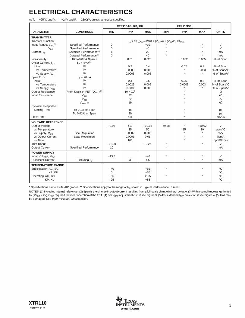
PIN CONFIGURATION
1
2
3
4
5
6
7
8
16
15
14
13
12
11
10
9
Source Resistor
Common
VREF In
VIN1 (10V)
VIN2 (5V)
Zero Adjust
Zero Adjust
Span Adjust
+VCC
VREF Force
Gate Drive
Source Sense
VREF Sense
VREF Adjust
4mA Span
16mA Span
TOP VIEW
ABSOLUTE MAXIMUM RATINGS(1)
Power Supply, +VCC ............................................................................ 40VInput Voltage, VIN1, VIN2, VREF IN ....................................................... +VCC
See text regarding safe negative input voltage range.Storage Temperature Range: A, B ................................ –55°C to +125°C
K, U ..................................–40°C to +85°COutput Short-Circuit Duration, Gate Drive and VREF Force ................................ Continuous to common and +VCC
Output Current Using Internal 50Ω Resistor ................................... 40mA
NOTE: (1) Stresses above these ratings may cause permanent damage.Exposure to absolute maximum conditions for extended periods may degradedevice reliability.
ELECTROSTATICDISCHARGE SENSITIVITY
This integrated circuit can be damaged by ESD. Texas Instrumentsrecommends that all integrated circuits be handled with appropriateprecautions. Failure to observe proper handling and installation proce-dures can cause damage.
ESD damage can range from subtle performance degradation tocomplete device failure. Precision integrated circuits may be moresusceptible to damage because very small parametric changes couldcause the device not to meet its published specifications.
PACKAGE TEMPERATUREPRODUCT PACKAGE-LEAD DESIGNATOR RANGE
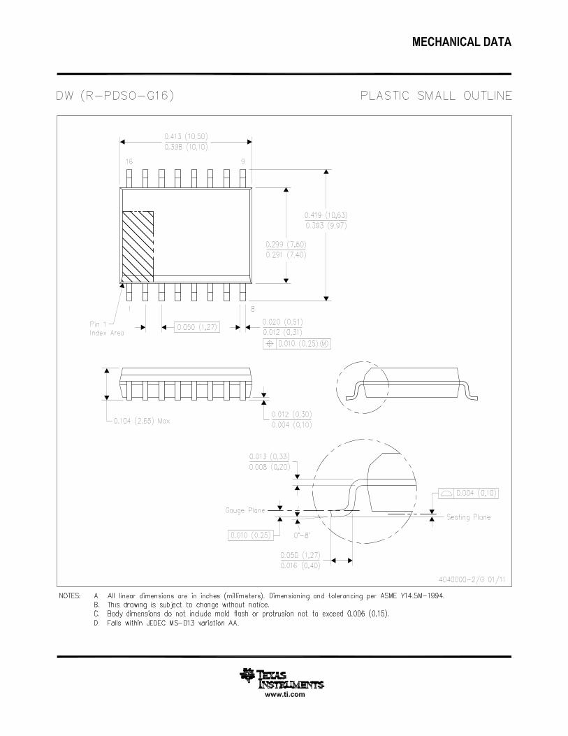
XTR110AG DIP-16 Ceramic JD –40°C to +85°CXTR110BG DIP-16 Ceramic JD –40°C to +85°CXTR110KP DIP-16 Plastic N 0°C to +70°CXTR110KU SOL-16 Surface-Mount DW 0°C to +70°C
NOTE: (1) For the most current package and ordering information, see the Package Option Addendum at the end of this document, or see the TI website at www.ti.com.
PACKAGE/ORDERING INFORMATION(1)
XTR110 3SBOS141C www.ti.com
XTR110AG, KP, KU XTR110BG
PARAMETER CONDITIONS MIN TYP MAX MIN TYP MAX UNITS
TRANSMITTERTransfer FunctionInput Range: VIN1
(5) Specified Performance 0 +10 * * VVIN2 Specified Performance 0 +5 * * V
Current, IO Specified Performance(1) 4 20 * * mADerated Performance(1) 0 40 * * mA
Nonlinearity 16mA/20mA Span(2) 0.01 0.025 0.002 0.005 % of SpanOffset Current, IOS IO = 4mA(1)
Initial (1) 0.2 0.4 0.02 0.1 % of Spanvs Temperature (1) 0.0003 0.005 * 0.003 % of Span/°Cvs Supply, VCC
(1) 0.0005 0.005 * * % of Span/VSpan Error IO = 20mA
Initial (1) 0.3 0.6 0.05 0.2 % of Spanvs Temperature (1) 0.0025 0.005 0.0009 0.003 % of Span/°Cvs Supply, VCC
(1) 0.003 0.005 * * % of Span/VOutput Resistance From Drain of FET (QEXT)(3) 10 x 109 * ΩInput Resistance VIN1 27 * kΩ
VIN2 22 * kΩVREF In 19 * kΩ
Dynamic ResponseSettling Time To 0.1% of Span 15 * µs
To 0.01% of Span 20 * µsSlew Rate 1.3 * mA/µs
VOLTAGE REFERENCEOutput Voltage +9.95 +10 +10.05 +9.98 * +10.02 V
vs Temperature 35 50 15 30 ppm/°Cvs Supply, VCC Line Regulation 0.0002 0.005 * * %/Vvs Output Current Load Regulation 0.0005 0.01 * * %/mAvs Time 100 * ppm/1k hrs
Trim Range –0.100 +0.25 * * VOutput Current Specified Performance 10 * mA
POWER SUPPLYInput Voltage, VCC +13.5 +40 * * VQuiescent Current Excluding IO 3 4.5 * * mA
TEMPERATURE RANGESpecification: AG, BG –40 +85 * * °C
KP, KU 0 +70 °COperating: AG, BG –55 +125 * * °C
KP, KU –25 +85 °C
ELECTRICAL CHARACTERISTICSAt TA = +25°C and VCC = +24V and RL = 250Ω**, unless otherwise specified.
IO = 10 [(VREFIn/16) + (VIN1/4) + (VIN2/2)] /RSPAN
* Specifications same as AG/KP grades. ** Specifications apply to the range of RL shown in Typical Performance Curves.
NOTES: (1) Including internal reference. (2) Span is the change in output current resulting from a full-scale change in input voltage. (3) Within compliance range limitedby (+VCC – 2V) +VDS required for linear operation of the FET. (4) For VREF adjustment circuit see Figure 3. (5) For extended IREF drive circuit see Figure 4. (5) Unit maybe damaged. See Input Voltage Range section.
XTR1104SBOS141Cwww.ti.com
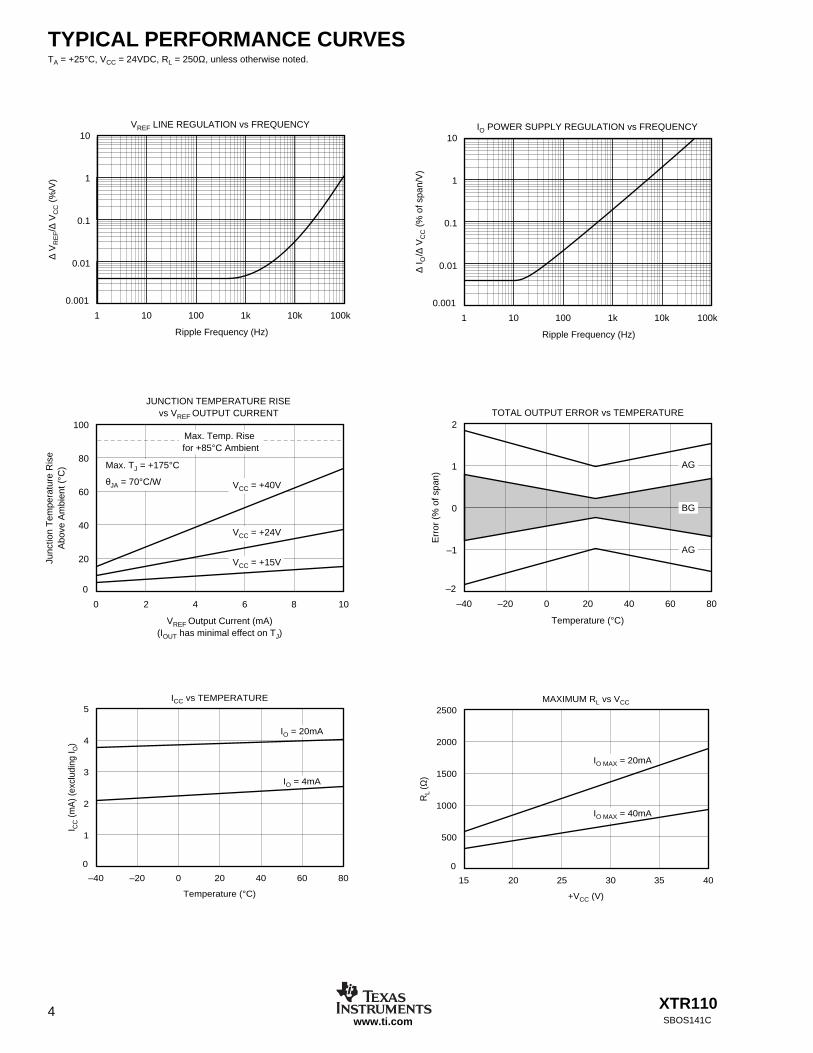
0
Temperature (°C)
ICC vs TEMPERATURE
–40
5
4
3
2
1
–20 0 20 40 60 80
I CC (m
A) (
excl
udin
g I O
)
IO = 20mA
IO = 4mA
0
+VCC (V)
MAXIMUM RL vs VCC
RL
(Ω)
2500
2000
1500
1000
500
20 3515 4025 30
IO MAX = 20mA
IO MAX = 40mA
TYPICAL PERFORMANCE CURVESTA = +25°C, VCC = 24VDC, RL = 250Ω, unless otherwise noted.
0.001
VREF LINE REGULATION vs FREQUENCY
∆ V
RE
F/∆
VC
C (
%/V
)
10
1
0.1
0.01
1 10 100 1k 10k 100k
Ripple Frequency (Hz)
0.001
IO POWER SUPPLY REGULATION vs FREQUENCY
∆ I O
/∆ V
CC (
% o
f spa
n/V
)
10
1
0.1
0.01
1 10 100 1k 10k 100k
Ripple Frequency (Hz)
Temperature (°C)
TOTAL OUTPUT ERROR vs TEMPERATURE
–40 –20 0 20 40 60 80
Err
or (
% o
f spa
n)
–2
2
1
0
–1
BG
AG
AG
0
VREF Output Current (mA)(IOUT has minimal effect on TJ)
JUNCTION TEMPERATURE RISE vs VREF OUTPUT CURRENT
Junc
tion
Tem
pera
ture
Ris
eA
bove
Am
bien
t (°C
)
100
80
60
40
20
2 80 104 6
VCC = +40V
VCC = +15V
VCC = +24V
Max. TJ = +175°C
Max. Temp. Rise for +85°C Ambient
θJA = 70°C/W
XTR110 5SBOS141C www.ti.com
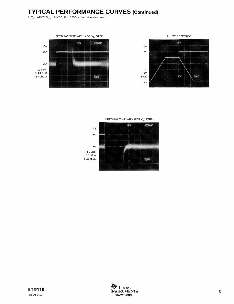
TYPICAL PERFORMANCE CURVES (Continued)At TA = +25°C, VCC = 24VDC, RL = 250Ω, unless otherwise noted.
SETTLING TIME WITH POS VIN STEP
VIN
0V
0V
IO Error(0.01% of
Span/Box)
SETTLING TIME WITH NEG VIN STEP
VIN
0V
0V
IO Error(0.01% of
Span/Box)
PULSE RESPONSE
VIN
0V
IOinto
500Ω
0V
XTR1106SBOS141Cwww.ti.com
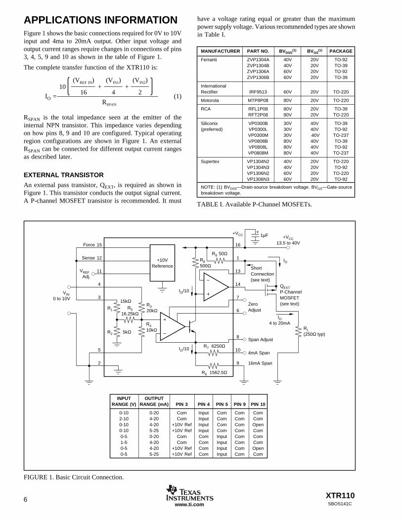
APPLICATIONS INFORMATIONFigure 1 shows the basic connections required for 0V to 10Vinput and 4ma to 20mA output. Other input voltage andoutput current ranges require changes in connections of pins3, 4, 5, 9 and 10 as shown in the table of Figure 1.
The complete transfer function of the XTR110 is:
IO = (1)
RSPAN is the total impedance seen at the emitter of theinternal NPN transistor. This impedance varies dependingon how pins 8, 9 and 10 are configured. Typical operatingregion configurations are shown in Figure 1. An externalRSPAN can be connected for different output current rangesas described later.
EXTERNAL TRANSISTOR
An external pass transistor, QEXT, is required as shown inFigure 1. This transistor conducts the output signal current.A P-channel MOSFET transistor is recommended. It must
(VREF IN)
16
(VIN1)
410 + +
(VIN2)
2
RSPAN
FIGURE 1. Basic Circuit Connection.
INPUT OUTPUTRANGE (V) RANGE (mA) PIN 3 PIN 4 PIN 5 PIN 9 PIN 10
0-10 0-20 Com Input Com Com Com2-10 4-20 Com Input Com Com Com0-10 4-20 +10V Ref Input Com Com Open0-10 5-25 +10V Ref Input Com Com Com0-5 0-20 Com Com Input Com Com1-5 4-20 Com Com Input Com Com0-5 4-20 +10V Ref Com Input Com Open0-5 5-25 +10V Ref Com Input Com Com
MANUFACTURER PART NO. BVDSS(1) BVGS
(1) PACKAGE
Ferranti ZVP1304A 40V 20V TO-92ZVP1304B 40V 20V TO-39ZVP1306A 60V 20V TO-92ZVP1306B 60V 20V TO-39
InternationalRectifier IRF9513 60V 20V TO-220
Motorola MTP8P08 80V 20V TO-220
RCA RFL1P08 80V 20V TO-39RFT2P08 80V 20V TO-220
Siliconix VP0300B 30V 40V TO-39(preferred) VP0300L 30V 40V TO-92
VP0300M 30V 40V TO-237VP0808B 80V 40V TO-39VP0808L 80V 40V TO-92VP0808M 80V 40V TO-237
Supertex VP1304N2 40V 20V TO-220VP1304N3 40V 20V TO-92VP1306N2 60V 20V TO-220VP1306N3 60V 20V TO-92
NOTE: (1) BVDSS—Drain-source breakdown voltage. BVGS—Gate-sourcebreakdown voltage.
TABLE I. Available P-Channel MOSFETs.
R516.25kΩ
16
1
13
14
7
6
8
10
9
15
12
11
4
3
5
2
R7 6250Ω
R6 1562.5Ω
R9 50Ω
R410kΩ
R320kΩ
R2
R1
R8500Ω
+10VReference
Zero Adjust
1µF+
+VCC13.5 to 40V
Span Adjust
4mA Span
RL(250Ω typ)
IO4 to 20mA
QEXTP-ChannelMOSFET(see text)
IO
IO/10
IO/10
VREF Adj.
Force
Sense
VIN 0 to 10V
ShortConnection(see text)
+VCC
16mA Span
5kΩ
15kΩ
have a voltage rating equal or greater than the maximumpower supply voltage. Various recommended types are shownin Table I.
XTR110 7SBOS141C www.ti.com
If the supply voltage, +VCC, exceeds the gate-to-sourcebreakdown voltage of QEXT, and the output connection(drain of QEXT) is broken, QEXT could fail. If the gate-to-source breakdown voltage is lower than +VCC, QEXT can beprotected with a 12V zener diode connected from gate tosource.
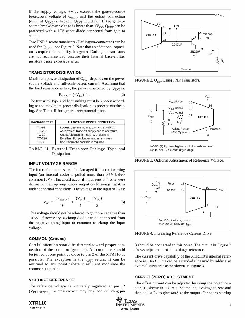
Two PNP discrete transistors (Darlington-connected) can beused for QEXT—see Figure 2. Note that an additional capaci-tor is required for stability. Integrated Darlington transistorsare not recommended because their internal base-emitterresistors cause excessive error.
TRANSISTOR DISSIPATION
Maximum power dissipation of QEXT depends on the powersupply voltage and full-scale output current. Assuming thatthe load resistance is low, the power dissipated by QEXT is:
PMAX = (+VCC) IFS (2)
The transistor type and heat sinking must be chosen accord-ing to the maximum power dissipation to prevent overheat-ing. See Table II for general recommendations.
PACKAGE TYPE ALLOWABLE POWER DISSIPATION
TO-92 Lowest: Use minimum supply and at +25°C.TO-237 Acceptable: Trade-off supply and temperature.TO-39 Good: Adequate for majority of designs.TO-220 Excellent: For prolonged maximum stress.TO-3 Use if hermetic package is required.
TABLE II. External Transistor Package Type andDissipation.
INPUT VOLTAGE RANGE
The internal op amp A1 can be damaged if its non-invertinginput (an internal node) is pulled more than 0.5V belowcommon (0V). This could occur if input pins 3, 4 or 5 weredriven with an op amp whose output could swing negativeunder abnormal conditions. The voltage at the input of A1 is:
VA1 = + + (3)
This voltage should not be allowed to go more negative than–0.5V. If necessary, a clamp diode can be connected fromthe negative-going input to common to clamp the inputvoltage.
COMMON (Ground)
Careful attention should be directed toward proper con-nection of the common (grounds). All commons shouldbe joined at one point as close to pin 2 of the XTR110 aspossible. The exception is the IOUT return. It can bereturned to any point where it will not modulate thecommon at pin 2.
VOLTAGE REFERENCE
The reference voltage is accurately regulated at pin 12(VREF SENSE). To preserve accuracy, any load including pin
(VREF IN)
16
(VIN1)
4
(VIN2)
2
FIGURE 2. QEXT
Using PNP Transistors.
XTR110
47nF
RL
IOUT
1
13
14
+VCC
16
2
2N2907etc.
TIP30Betc.
0.047µF
Common
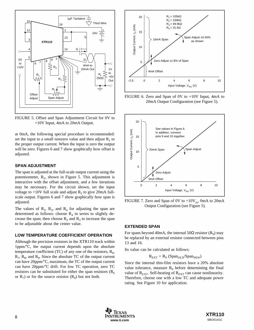
3 should be connected to this point. The circuit in Figure 3shows adjustment of the voltage reference.
The current drive capability of the XTR110’s internal refer-ence is 10mA. This can be extended if desired by adding anexternal NPN transistor shown in Figure 4.
OFFSET (ZERO) ADJUSTMENT
The offset current can be adjusted by using the potentiom-eter, R1, shown in Figure 5. Set the input voltage to zero andthen adjust R1 to give 4mA at the output. For spans starting
FIGURE 4. Increasing Reference Current Drive.
XTR110
15
12 +VCC16
2
Sense
Force
For 100mA with VCC up to 40V use 2N3055 for QREF.
QREF
+10VREF
FIGURE 3. Optional Adjustment of Reference Voltage.
XTR110
VREF Adjust
15
12
11
VREF Sense
VREF Force
+VCC
16
Common2
VREF
R20kΩ
RS(1)
Adjust Range±5% Optimum
NOTE: (1) RS gives higher resolution with reducedrange, set RS = 0Ω for larger range.
XTR1108SBOS141Cwww.ti.com
FIGURE 6. Zero and Span of 0V to +10V Input, 4mA to20mA Output Configuration (see Figure 5).
FIGURE 7. Zero and Span of 0V to +10VIN
, 0mA to 20mAOutput Configuration (see Figure 5).
at 0mA, the following special procedure is recommended:set the input to a small nonzero value and then adjust R1 tothe proper output current. When the input is zero the outputwill be zero. Figures 6 and 7 show graphically how offset isadjusted.
SPAN ADJUSTMENT
The span is adjusted at the full-scale output current using thepotentiometer, R2, shown in Figure 5. This adjustment isinteractive with the offset adjustment, and a few iterationsmay be necessary. For the circuit shown, set the inputvoltage to +10V full scale and adjust R2 to give 20mA full-scale output. Figures 6 and 7 show graphically how span isadjusted.
The values of R2, R3, and R4 for adjusting the span aredetermined as follows: choose R4 in series to slightly de-crease the span; then choose R2 and R3 to increase the spanto be adjustable about the center value.
LOW TEMPERATURE COEFFICIENT OPERATION
Although the precision resistors in the XTR110 track within1ppm/°C, the output current depends upon the absolutetemperature coefficient (TC) of any one of the resistors, R6,R7, R8, and R9. Since the absolute TC of the output currentcan have 20ppm/°C, maximum, the TC of the output currentcan have 20ppm/°C drift. For low TC operation, zero TCresistors can be substituted for either the span resistors (R6or R7) or for the source resistor (R9) but not both.
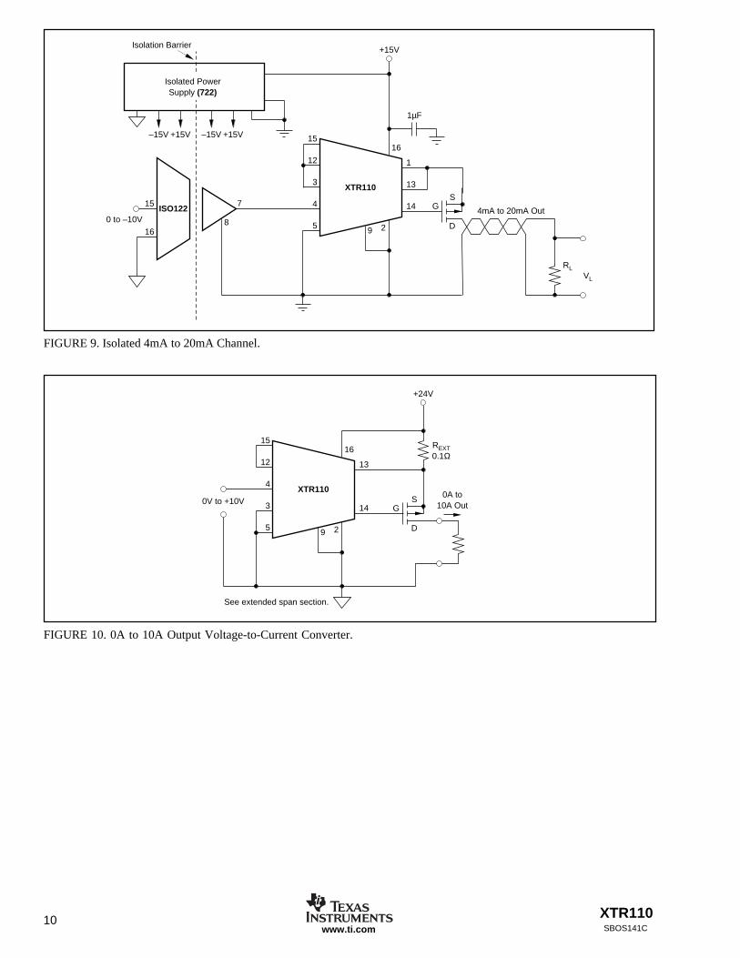
EXTENDED SPAN
For spans beyond 40mA, the internal 50Ω resistor (R9) maybe replaced by an external resistor connected between pins13 and 16.
Its value can be calculated as follows:
REXT = R9 (SpanOLD/SpanNEW)
Since the internal thin-film resistors have a 20% absolutevalue tolerance, measure R9 before determining the finalvalue of REXT. Self-heating of REXT can cause nonlinearity.Therefore, choose one with a low TC and adequate powerrating. See Figure 10 for application.
FIGURE 5. Offset and Span Adjustment Circuit for 0V to+10V Input, 4mA to 20mA Output. 20
15
10
5
0 2 4 6 8 10
Input Voltage, VIN1 (V)
Out
put C
urre
nt, I
O (
mA
)
0mA Offset
Zero Adjust
Span Adjust20mA Span
See values in Figure 6.In addition, connectpins 9 and 10 together.
XTR110
15
1Vto+5VOut
1
13
16
2
R4
S
G
D
+
–
9876
R1
R2
R3
Span AdjustOffsetAdjust
0Vto
+10V4mA to
20mA Out
RL250Ω
24V
1µF Tantalum
Third Wire
14
12
3
4
5
20
15
10
5
0 2 4 6 8 10
Input Voltage, VIN1 (V)
Out
put C
urre
nt, I
O (
mA
)
4mA Offset
Zero Adjust ±1.8% of Span
Span Adjust ±0.45%as shown16mA Span
R1 = 100kΩR2 = 100kΩR3 = 49.9kΩR4 = 31.6Ω
−2.5

XTR110 9SBOS141C www.ti.com
TYPICAL APPLICATIONSThe XTR110 is ideal for a variety of applications requiringhigh noise immunity current-mode signal transmission. Theprecision +10V reference can be used to excite bridges andtransducers. Selectable ranges make it very useful as aprecision programmable current source. The compact design
and low price of the XTR110 allow versatility with aminimum of external components and design engineeringexpense.
Figures 8 through 10 show typical applications of theXTR110.
FIGURE 8. ±200mA Current Pump.
16
1
13
14
7
6
8
10
9
15
12
11
4
3
5
2
+10VReference
+15V
A4
A3
R915kΩ
R101kΩ
OffsetAdjust
R320kΩ
R52MΩ
A2
R42kΩ
T3
A1
R24.99Ω
R74.75kΩ
R6402Ω
R8 200ΩFine Trim
RH 50kΩCoarse Trim
R12Ω
T2
–15V
IO
SpanAdjust
VIN
VIN (V)
105
0
200
–200
IO (mA) R1, R2: Low TC resistors to dissipate 0.32W continuous power.For other current ranges, scale both resistors proportionately.
R8, R10, R11: 10-turn trimpots for greatest sensitivity.R6, R7: Low TC resistors.A1 - A4: 1/4 LM324 (powered by ±15V).
T1: International Rectifier IR9513(1).T2: International Rectifier IR513(1).T3: International Rectifier IRFF9113(1).
NOTE: (1) Or other adequate power rating MOS transistor.
T1
XTR11010SBOS141Cwww.ti.com
FIGURE 9. Isolated 4mA to 20mA Channel.
FIGURE 10. 0A to 10A Output Voltage-to-Current Converter.
15
12
4
3
5
13
14
16
2
SG
D9
XTR1100A to
10A Out
See extended span section.
0V to +10V
+24V
REXT0.1Ω
15
12
3
4
5
1
13
14
16
2
SG
D9
1µF
XTR110
VL
4mA to 20mA Out
RL
ISO122
–15V +15V +15V–15V
15
816
7
Isolated PowerSupply (722)
Isolation Barrier +15V
0 to –10V
XTR110 11SBOS141C www.ti.com
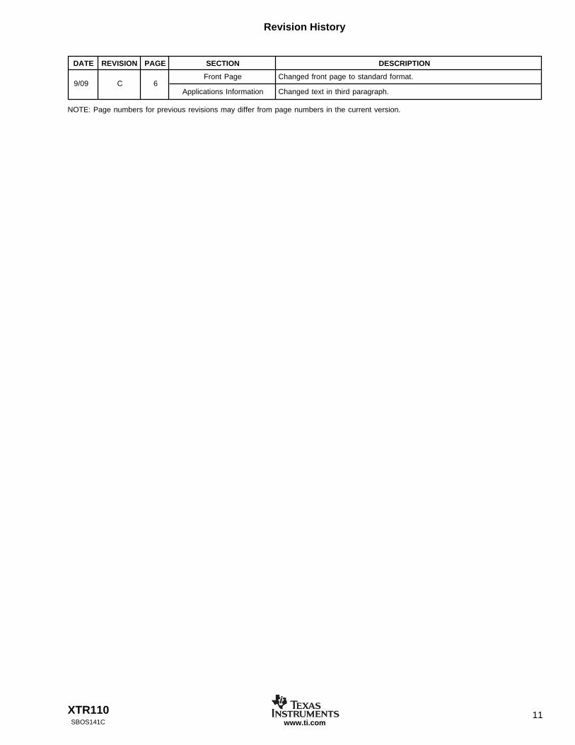
DATE REVISION PAGE SECTION DESCRIPTION
Front Page Changed front page to standard format.
Applications Information Changed text in third paragraph.
Revision History
NOTE: Page numbers for previous revisions may differ from page numbers in the current version.
9/09 C 6

PACKAGING INFORMATION
Orderable Device Status (1) PackageType
PackageDrawing
Pins PackageQty
Eco Plan (2) Lead/Ball Finish MSL Peak Temp (3)
XTR110AD OBSOLETE DIESALE Y 0 TBD Call TI Call TI
XTR110AG NRND CDIP SB JD 16 1 Green (RoHS &no Sb/Br)
AU N / A for Pkg Type
XTR110BG NRND CDIP SB JD 16 1 Green (RoHS &no Sb/Br)
AU N / A for Pkg Type
XTR110KP ACTIVE PDIP N 16 25 Green (RoHS &no Sb/Br)
CU NIPDAU N / A for Pkg Type
XTR110KPG4 ACTIVE PDIP N 16 25 Green (RoHS &no Sb/Br)
CU NIPDAU N / A for Pkg Type
XTR110KU ACTIVE SOIC DW 16 40 Green (RoHS &no Sb/Br)
CU NIPDAU Level-3-260C-168 HR
XTR110KU/1K ACTIVE SOIC DW 16 1000 Green (RoHS &no Sb/Br)
CU NIPDAU Level-3-260C-168 HR
XTR110KU/1KG4 ACTIVE SOIC DW 16 1000 Green (RoHS &no Sb/Br)
CU NIPDAU Level-3-260C-168 HR
XTR110KUG4 ACTIVE SOIC DW 16 40 Green (RoHS &no Sb/Br)
CU NIPDAU Level-3-260C-168 HR
(1) The marketing status values are defined as follows:ACTIVE: Product device recommended for new designs.LIFEBUY: TI has announced that the device will be discontinued, and a lifetime-buy period is in effect.NRND: Not recommended for new designs. Device is in production to support existing customers, but TI does not recommend using this part ina new design.PREVIEW: Device has been announced but is not in production. Samples may or may not be available.OBSOLETE: TI has discontinued the production of the device.
(2) Eco Plan - The planned eco-friendly classification: Pb-Free (RoHS), Pb-Free (RoHS Exempt), or Green (RoHS & no Sb/Br) - please checkhttp://www.ti.com/productcontent for the latest availability information and additional product content details.TBD: The Pb-Free/Green conversion plan has not been defined.Pb-Free (RoHS): TI's terms "Lead-Free" or "Pb-Free" mean semiconductor products that are compatible with the current RoHS requirementsfor all 6 substances, including the requirement that lead not exceed 0.1% by weight in homogeneous materials. Where designed to be solderedat high temperatures, TI Pb-Free products are suitable for use in specified lead-free processes.Pb-Free (RoHS Exempt): This component has a RoHS exemption for either 1) lead-based flip-chip solder bumps used between the die andpackage, or 2) lead-based die adhesive used between the die and leadframe. The component is otherwise considered Pb-Free (RoHScompatible) as defined above.Green (RoHS & no Sb/Br): TI defines "Green" to mean Pb-Free (RoHS compatible), and free of Bromine (Br) and Antimony (Sb) based flameretardants (Br or Sb do not exceed 0.1% by weight in homogeneous material)
(3) MSL, Peak Temp. -- The Moisture Sensitivity Level rating according to the JEDEC industry standard classifications, and peak soldertemperature.
Important Information and Disclaimer:The information provided on this page represents TI's knowledge and belief as of the date that it isprovided. TI bases its knowledge and belief on information provided by third parties, and makes no representation or warranty as to theaccuracy of such information. Efforts are underway to better integrate information from third parties. TI has taken and continues to takereasonable steps to provide representative and accurate information but may not have conducted destructive testing or chemical analysis onincoming materials and chemicals. TI and TI suppliers consider certain information to be proprietary, and thus CAS numbers and other limitedinformation may not be available for release.
In no event shall TI's liability arising out of such information exceed the total purchase price of the TI part(s) at issue in this document sold by TIto Customer on an annual basis.
PACKAGE OPTION ADDENDUM
www.ti.com 8-Sep-2009
Addendum-Page 1

TAPE AND REEL INFORMATION
*All dimensions are nominal
Device PackageType
PackageDrawing
Pins SPQ ReelDiameter
(mm)
ReelWidth
W1 (mm)
A0(mm)
B0(mm)
K0(mm)
P1(mm)
W(mm)
Pin1Quadrant
XTR110KU/1K SOIC DW 16 1000 330.0 16.4 10.75 10.7 2.7 12.0 16.0 Q1
PACKAGE MATERIALS INFORMATION
www.ti.com 14-Jul-2012
Pack Materials-Page 1

*All dimensions are nominal
Device Package Type Package Drawing Pins SPQ Length (mm) Width (mm) Height (mm)
XTR110KU/1K SOIC DW 16 1000 367.0 367.0 38.0
PACKAGE MATERIALS INFORMATION
www.ti.com 14-Jul-2012
Pack Materials-Page 2


IMPORTANT NOTICE
Texas Instruments Incorporated and its subsidiaries (TI) reserve the right to make corrections, enhancements, improvements and otherchanges to its semiconductor products and services per JESD46C and to discontinue any product or service per JESD48B. Buyers shouldobtain the latest relevant information before placing orders and should verify that such information is current and complete. Allsemiconductor products (also referred to herein as “components”) are sold subject to TI’s terms and conditions of sale supplied at the timeof order acknowledgment.
TI warrants performance of its components to the specifications applicable at the time of sale, in accordance with the warranty in TI’s termsand conditions of sale of semiconductor products. Testing and other quality control techniques are used to the extent TI deems necessaryto support this warranty. Except where mandated by applicable law, testing of all parameters of each component is not necessarilyperformed.
TI assumes no liability for applications assistance or the design of Buyers’ products. Buyers are responsible for their products andapplications using TI components. To minimize the risks associated with Buyers’ products and applications, Buyers should provideadequate design and operating safeguards.
TI does not warrant or represent that any license, either express or implied, is granted under any patent right, copyright, mask work right, orother intellectual property right relating to any combination, machine, or process in which TI components or services are used. Informationpublished by TI regarding third-party products or services does not constitute a license to use such products or services or a warranty orendorsement thereof. Use of such information may require a license from a third party under the patents or other intellectual property of thethird party, or a license from TI under the patents or other intellectual property of TI.
Reproduction of significant portions of TI information in TI data books or data sheets is permissible only if reproduction is without alterationand is accompanied by all associated warranties, conditions, limitations, and notices. TI is not responsible or liable for such altereddocumentation. Information of third parties may be subject to additional restrictions.
Resale of TI components or services with statements different from or beyond the parameters stated by TI for that component or servicevoids all express and any implied warranties for the associated TI component or service and is an unfair and deceptive business practice.TI is not responsible or liable for any such statements.
Buyer acknowledges and agrees that it is solely responsible for compliance with all legal, regulatory and safety-related requirementsconcerning its products, and any use of TI components in its applications, notwithstanding any applications-related information or supportthat may be provided by TI. Buyer represents and agrees that it has all the necessary expertise to create and implement safeguards whichanticipate dangerous consequences of failures, monitor failures and their consequences, lessen the likelihood of failures that might causeharm and take appropriate remedial actions. Buyer will fully indemnify TI and its representatives against any damages arising out of the useof any TI components in safety-critical applications.
In some cases, TI components may be promoted specifically to facilitate safety-related applications. With such components, TI’s goal is tohelp enable customers to design and create their own end-product solutions that meet applicable functional safety standards andrequirements. Nonetheless, such components are subject to these terms.
No TI components are authorized for use in FDA Class III (or similar life-critical medical equipment) unless authorized officers of the partieshave executed a special agreement specifically governing such use.
Only those TI components which TI has specifically designated as military grade or “enhanced plastic” are designed and intended for use inmilitary/aerospace applications or environments. Buyer acknowledges and agrees that any military or aerospace use of TI componentswhich have not been so designated is solely at the Buyer's risk, and that Buyer is solely responsible for compliance with all legal andregulatory requirements in connection with such use.
TI has specifically designated certain components which meet ISO/TS16949 requirements, mainly for automotive use. Components whichhave not been so designated are neither designed nor intended for automotive use; and TI will not be responsible for any failure of suchcomponents to meet such requirements.
Products Applications
Audio www.ti.com/audio Automotive and Transportation www.ti.com/automotive
Amplifiers amplifier.ti.com Communications and Telecom www.ti.com/communications
Data Converters dataconverter.ti.com Computers and Peripherals www.ti.com/computers
DLP® Products www.dlp.com Consumer Electronics www.ti.com/consumer-apps
DSP dsp.ti.com Energy and Lighting www.ti.com/energy
Clocks and Timers www.ti.com/clocks Industrial www.ti.com/industrial
Interface interface.ti.com Medical www.ti.com/medical
Logic logic.ti.com Security www.ti.com/security
Power Mgmt power.ti.com Space, Avionics and Defense www.ti.com/space-avionics-defense
Microcontrollers microcontroller.ti.com Video and Imaging www.ti.com/video
RFID www.ti-rfid.com
OMAP Mobile Processors www.ti.com/omap TI E2E Community e2e.ti.com
Wireless Connectivity www.ti.com/wirelessconnectivity
Mailing Address: Texas Instruments, Post Office Box 655303, Dallas, Texas 75265Copyright © 2012, Texas Instruments Incorporated