wireless lan transceiver design and verificationme.fudan.edu.cn/download/rfic_2004_ofdm.pdfagilent...
TRANSCRIPT
Agilent Advanced RFIC Design Seminar
Wireless LAN Transceiver Design andVerification:
An Integrated Methodology for System and CircuitDesign in the Cadence IC Design Flow

Page 2
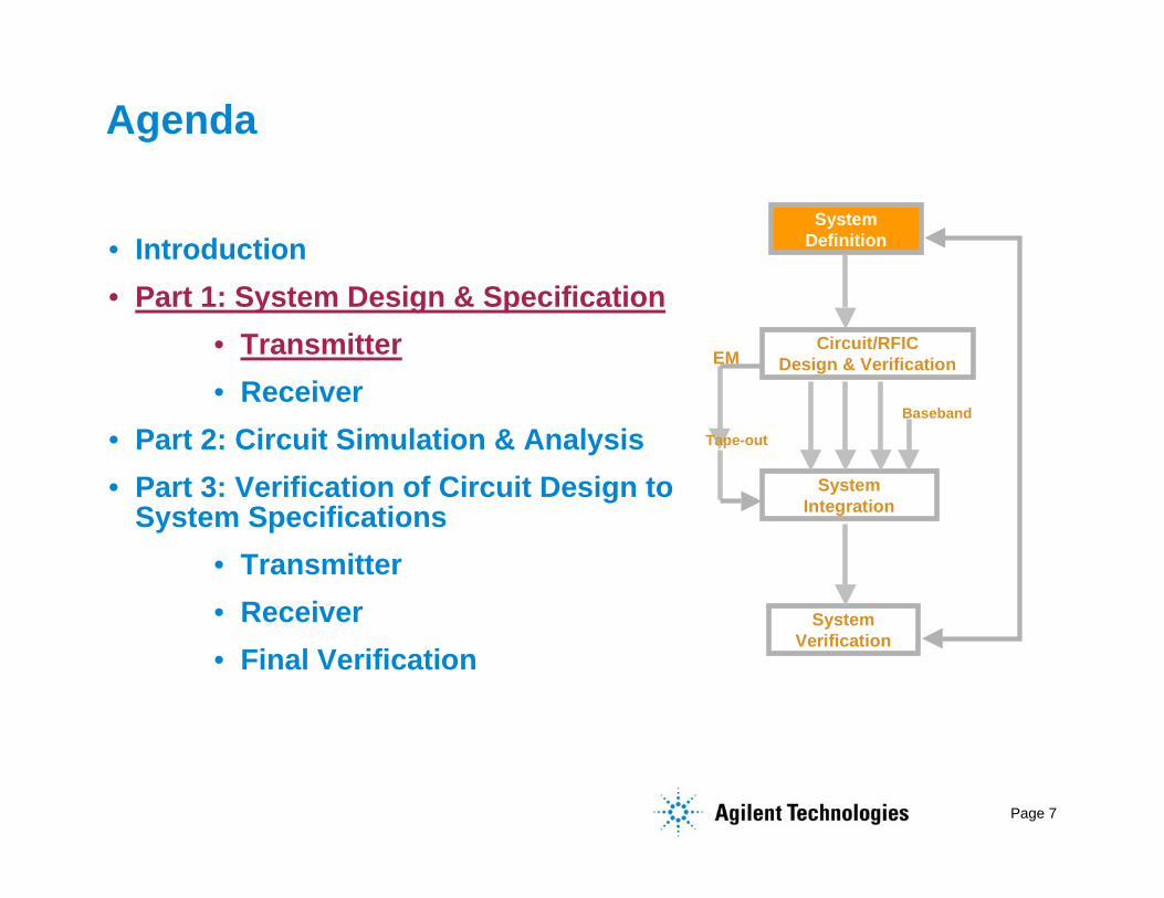
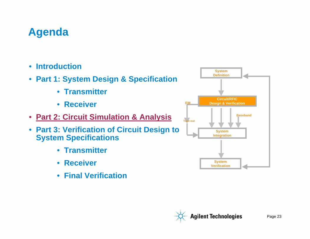
Agenda
• Introduction• Part 1: System Design & Specification
• Transmitter• Receiver
• Part 2: Circuit Simulation & Analysis• Part 3: Verification of Circuit Design
to System Specifications• Transmitter• Receiver• Final Verification
SystemDefinition
SystemVerification
Circuit/RFICDesign & Verification
SystemIntegration
BasebandTape-out
EM
Page 3
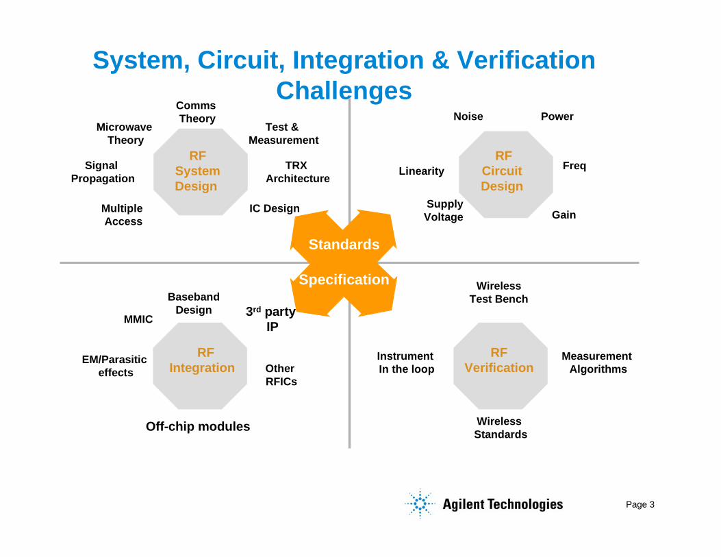
System, Circuit, Integration & VerificationChallenges
Comms Theory
TRX Architecture
IC Design
Test & Measurement
Multiple Access
Signal Propagation
Microwave Theory
RFSystemDesign
RFCircuit Design
Noise Power
Linearity
SupplyVoltage Gain
Freq
BasebandDesign
Off-chip modules
Other RFICs
3rd party IP
EM/Parasitic effects
MMIC
RF Integration
Instrument In the loop
Measurement Algorithms
Wireless Standards
WirelessTest Bench
RFVerification
Standards
Specification
Page 4
Specification-Driven RFIC Flow
New Flow:Continuous verification of a design
to system-level specifications,based on a wireless standard,throughout the design flow
Prototype Test
Communication SystemDesign
RF Block-Level CircuitDesign
RFIC Layout Design andVerification
TapeOut
System SpecsBER/PER
EVM
CCDF
…
Circuit SpecsNF
P1dB
TOI
…
CommunicationSystem Design
RF Block-LevelCircuit Design
RFIC Layout Designand Verification
Prototype Test
TapeOut
System SpecsBER/PER
EVM
CCDF
…
Circuit SpecsNF
P1dB
TOI
…
?
Traditional Flow:System Designers design to wireless
system-level specifications. RFICDesigners design to circuit-levelspecifications. Uncertainty due to lackof correlation

Page 5
Agilent Tools for Design & Verification
ModelGeneration
Ptolemy
TSDF
ENV Tran
WTB
AC/DC
HB
SP
MoM
SimulationTechnologies
Cosimulation &IP integration
SystemDefinition
SystemVerification
Circuit/RFICDesign & Verification
SystemIntegration
BasebandTape-out
EM
Hardware verificationwith Instrument
PC
Page 6
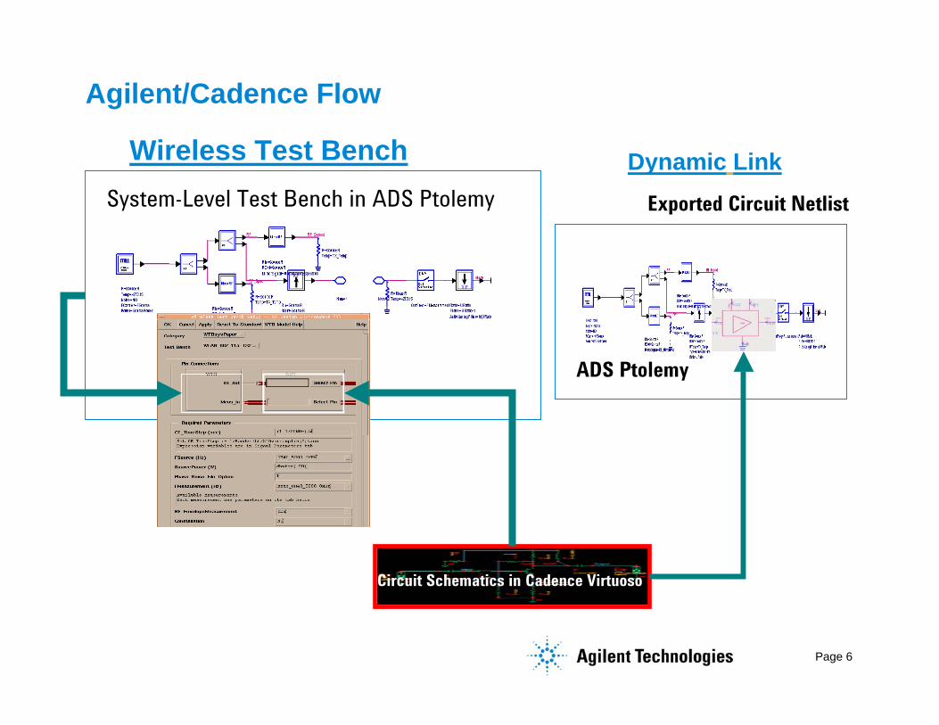
Agilent/Cadence Flow
System-Level Test Bench in ADS Ptolemy Exported Circuit Netlist
ADS Ptolemy
Dynamic Link
Circuit Schematics in Cadence Virtuoso
Wireless Test Bench
Page 7
Agenda
SystemDefinition
SystemVerification
Circuit/RFICDesign & Verification
SystemIntegration
Baseband
Tape-out
EM
pre/post-tapeout
• Introduction• Part 1: System Design & Specification
• Transmitter• Receiver
• Part 2: Circuit Simulation & Analysis• Part 3: Verification of Circuit Design to
System Specifications• Transmitter• Receiver• Final Verification
Page 8
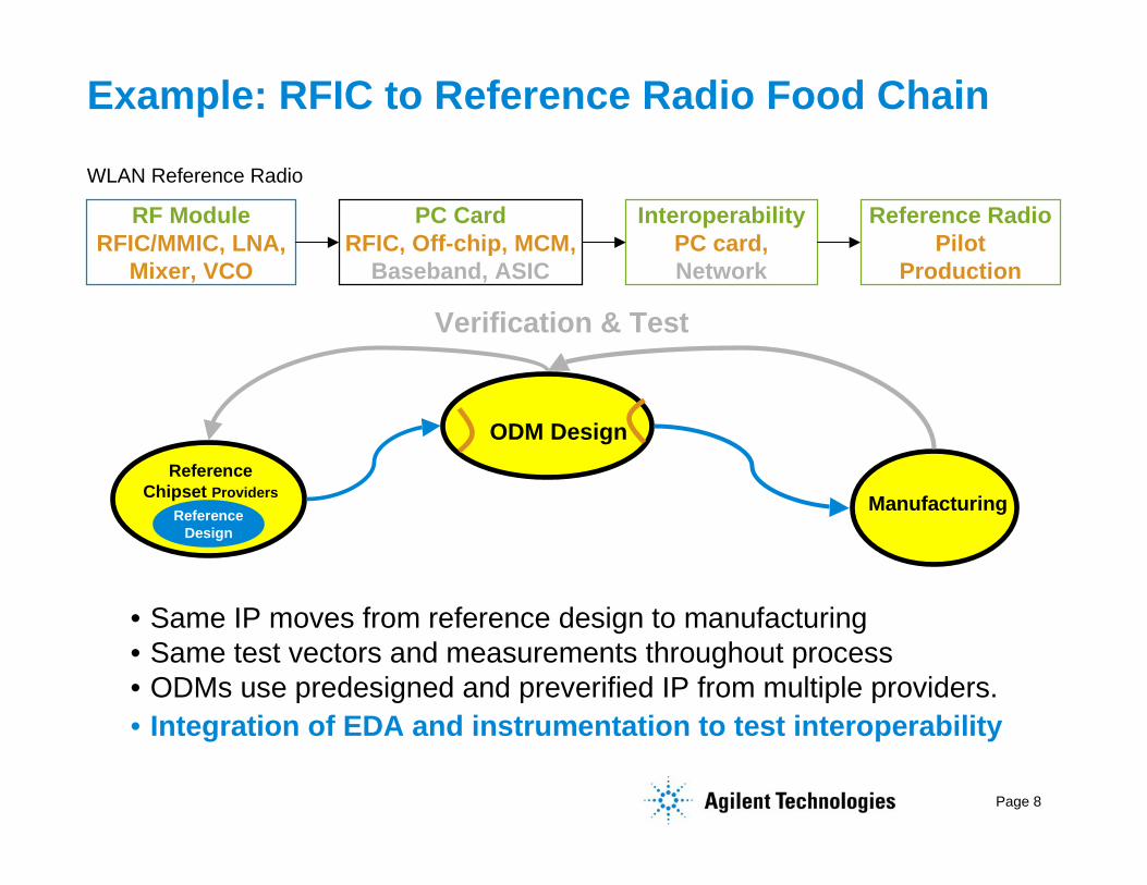
Example: RFIC to Reference Radio Food Chain
RF ModuleRFIC/MMIC, LNA,
Mixer, VCO
PC CardRFIC, Off-chip, MCM,
Baseband, ASIC
Reference RadioPilot
Production
• Same IP moves from reference design to manufacturing• Same test vectors and measurements throughout process• ODMs use predesigned and preverified IP from multiple providers.• Integration of EDA and instrumentation to test interoperability
Reference
Design
ReferenceChipset Providers Manufacturing
ODM Design
Verification & Test
InteroperabilityPC card,Network
WLAN Reference Radio
Page 9
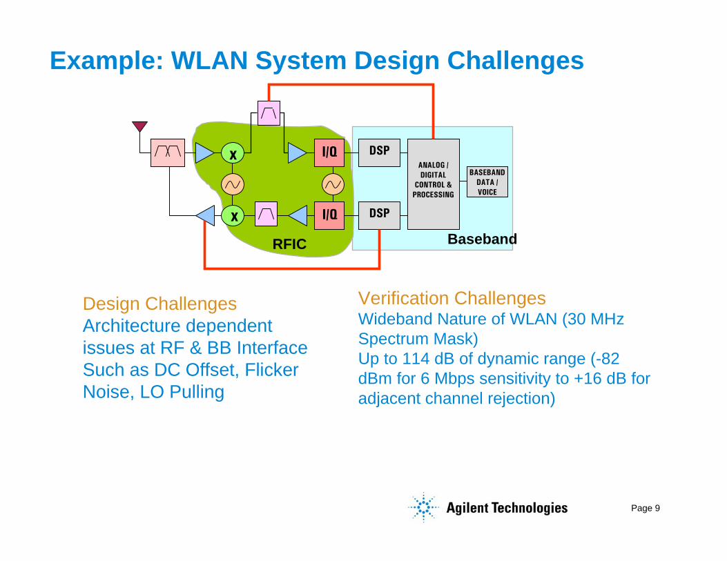
Example: WLAN System Design Challenges
x I/Q DSP
x
ANALOG /DIGITAL
CONTROL &PROCESSING
I/Q DSP
BASEBANDDATA /VOICE
BasebandRFIC
Design ChallengesArchitecture dependentissues at RF & BB InterfaceSuch as DC Offset, FlickerNoise, LO Pulling
Verification ChallengesWideband Nature of WLAN (30 MHzSpectrum Mask)Up to 114 dB of dynamic range (-82dBm for 6 Mbps sensitivity to +16 dB foradjacent channel rejection)

Page 10
Transmitter System Definition in ADS Ptolemy
• Baseband source
• EVM Measurement (algorithm)
1
25
4
3
• Modulator
• VCO & Mixer
• Cascaded pre-amp/PA +filters
Frequency = 5.15-5.35 GHzMaximum Data Rate = 54 MbpsOutput Power = 15 dBmModulation accuracy: -5 -25 dB EVMCarrier leakage: -15 dBrOut of band spectrum:
< -27 /-41 dBm EIRPPower Consumption 1.8 WSupply Voltage 3.3V
Page 11
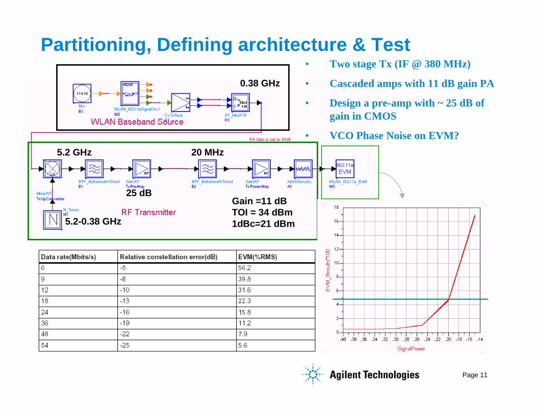
Partitioning, Defining architecture & Test
0.38 GHz
5.2-0.38 GHz
5.2 GHz 20 MHz
Gain =11 dBTOI = 34 dBm1dBc=21 dBm
25 dB
• Two stage Tx (IF @ 380 MHz)
• Cascaded amps with 11 dB gain PA
• Design a pre-amp with ~ 25 dB ofgain in CMOS
• VCO Phase Noise on EVM?
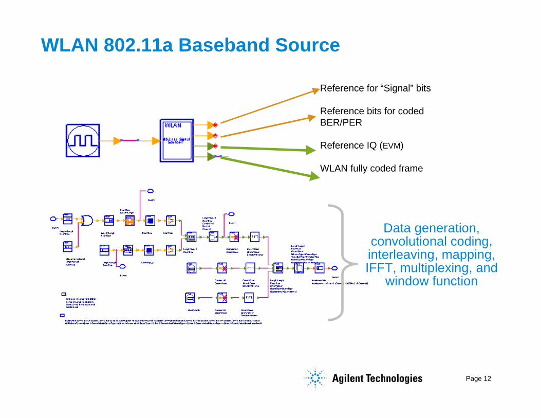
Page 12
Reference for “Signal” bits
Reference bits for codedBER/PER
Reference IQ (EVM)
WLAN fully coded frame
Data generation,convolutional coding,interleaving, mapping,IFFT, multiplexing, and
window function
WLAN 802.11a Baseband Source
Page 13
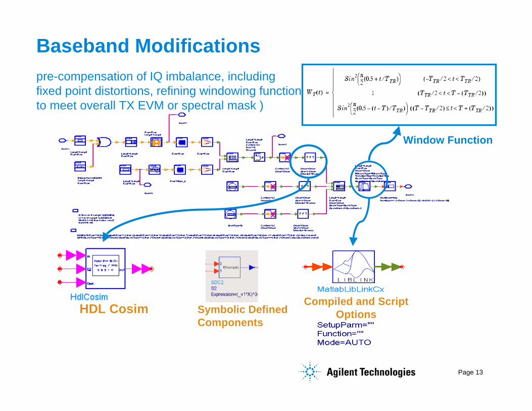
Baseband Modifications
Window Function
HDL Cosim Compiled and ScriptOptionsSymbolic Defined
Components
pre-compensation of IQ imbalance, includingfixed point distortions, refining windowing functionto meet overall TX EVM or spectral mask )
Page 14
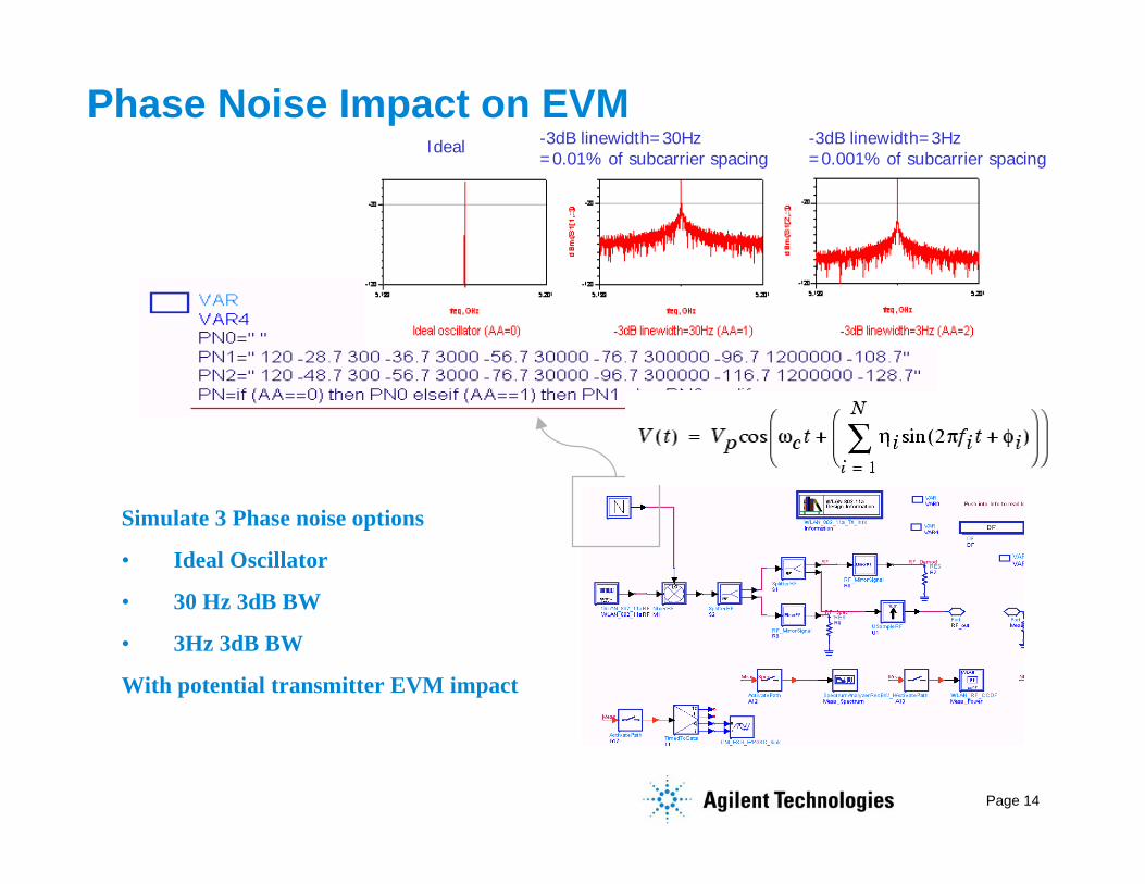
Phase Noise Impact on EVM
Simulate 3 Phase noise options
• Ideal Oscillator
• 30 Hz 3dB BW
• 3Hz 3dB BW
With potential transmitter EVM impact
Ideal -3dB linewidth=30Hz=0.01% of subcarrier spacing
-3dB linewidth=3Hz=0.001% of subcarrier spacing
Page 15
Agenda
• Introduction• Part 1: System Design & Specification
• Transmitter• Receiver
• Part 2: Circuit Simulation & Analysis• Part 3: Verification of Circuit Design to
System Specifications• Transmitter• Receiver• Final Verification

Page 16
Receiver System Specification for 802.11a
Input Signal Band 5.3 GHzReceiver NF 6 dB maxModulation (PSK+QAM) 4,16, 64 QAMOccupied BW 16.6 MHzChannel Spacing 20 MHzData Rate (Mbps) 6,9,12,18,24,
36,48,54Receiver EVM -28 dB (~4% rms)Receiver Dynamic Range -80 to -30 dBmPER < 10%
Page 17
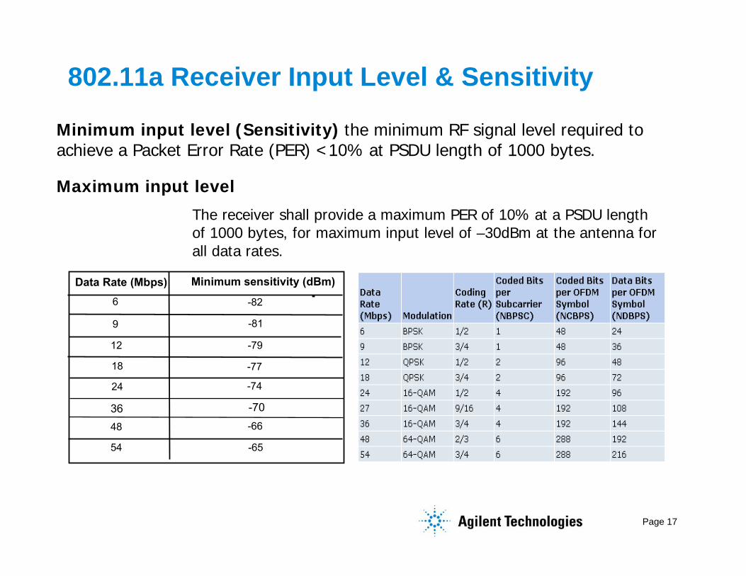
802.11a Receiver Input Level & Sensitivity
Data Rate (Mbps)
6
Minimum sensitivity (dBm)
-82
9
12
18
24
36
48
54
-81
-79
-77
-74
-70
-66
-65
Minimum input level (Sensitivity) the minimum RF signal level required toachieve a Packet Error Rate (PER) <10% at PSDU length of 1000 bytes.
Maximum input level
The receiver shall provide a maximum PER of 10% at a PSDU lengthof 1000 bytes, for maximum input level of –30dBm at the antenna forall data rates.
Page 18
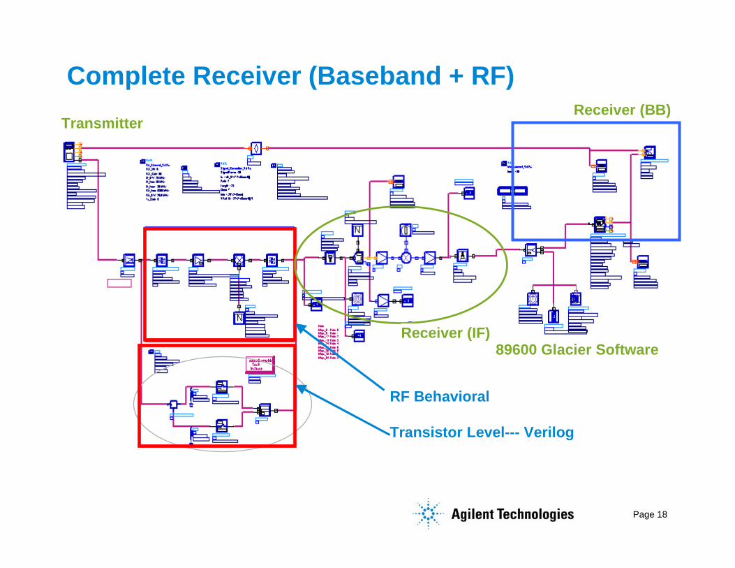
Complete Receiver (Baseband + RF)
RF Behavioral
Transistor Level--- Verilog
TransmitterReceiver (BB)
Receiver (IF)89600 Glacier Software
Page 19
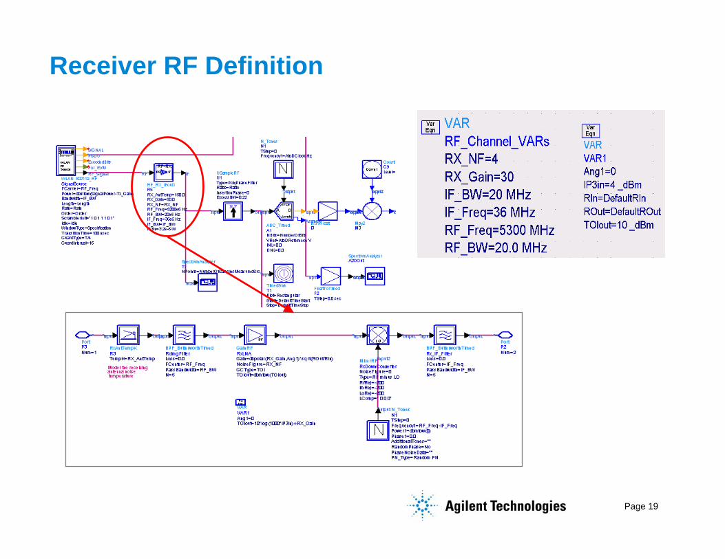
Receiver RF Definition
Page 20
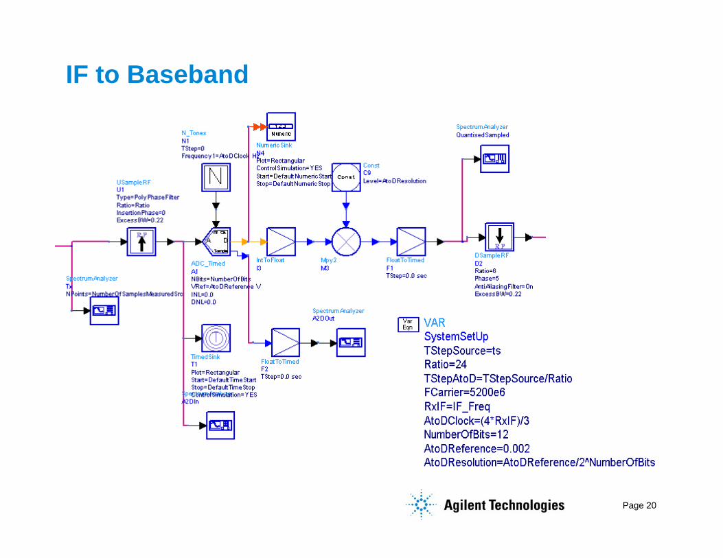
IF to Baseband
Page 21
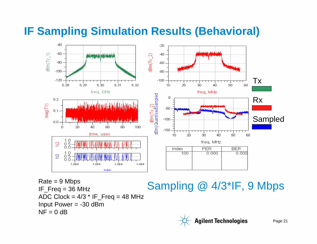
IF Sampling Simulation Results (Behavioral)
Rate = 9 MbpsIF_Freq = 36 MHzADC Clock = 4/3 * IF_Freq = 48 MHzInput Power = -30 dBmNF = 0 dB
Sampling @ 4/3*IF, 9 Mbps
Tx
Rx
Sampled

Page 22
Exploring the Impact of Receiver Noise Figure
Receiver Sensitivity @ -80 dBmcan tolerate a noise figurearound 7.5 dB
Page 23
Agenda
SystemDefinition
SystemVerification
Circuit/RFICDesign & Verification
SystemIntegration
BasebandTape-out
EM
• Introduction• Part 1: System Design & Specification
• Transmitter• Receiver
• Part 2: Circuit Simulation & Analysis• Part 3: Verification of Circuit Design to
System Specifications• Transmitter• Receiver• Final Verification
Page 24
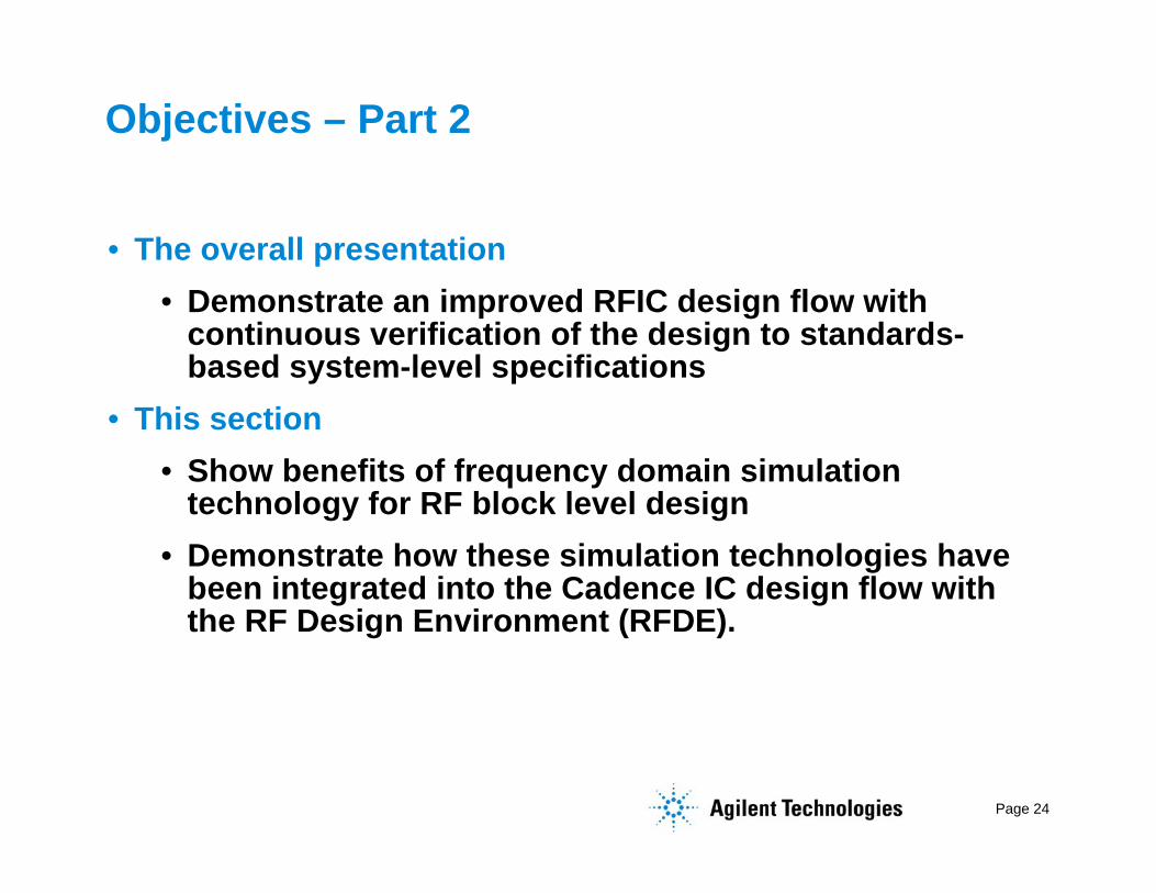
Objectives – Part 2
• The overall presentation• Demonstrate an improved RFIC design flow with
continuous verification of the design to standards-based system-level specifications
• This section• Show benefits of frequency domain simulation
technology for RF block level design• Demonstrate how these simulation technologies have
been integrated into the Cadence IC design flow withthe RF Design Environment (RFDE).

Page 25
Receiver front-end block diagram
÷2
MatchingNetwork
IM3 Suppression and IP3P-1 dBIP2Noise FigureOutput Noise FloorDynamic RangeLO drive levelQuadrature AccuracyAmplitude Balance
Frequency rangeI/Q Base-band Frequency rangeCarrier FeedthroughSideband Suppression

Page 26
Receiver front-end in Cadence Virtuoso

Page 27
System specifications and related circuitspecifications
CircuitInput Signal Band 5.3 GHz
Receiver NF < 6 dB
LO Phase Noise -110 dBc/Hz @1 MHz
Conversion Gain 30 dB
LNA 8 dB
Mixer 12 dB
IF Band 36 MHz
IIP3 (Mixer) > 5 dBm
P1dB -10 dBm
Input Dynamic Range -80 to -30 dBm
SystemInput Signal Band 5.3 GHz
Receiver NF 6 dB max
Modulation (PSK+QAM) 4,16,64 QAM
Occupied BW 16.6 MHz
Data Rate 6,9,12,18,24
,36,48,54
Receiver EVM -28 dB
PER {-30 to -80 dBm} < 10%
Page 28
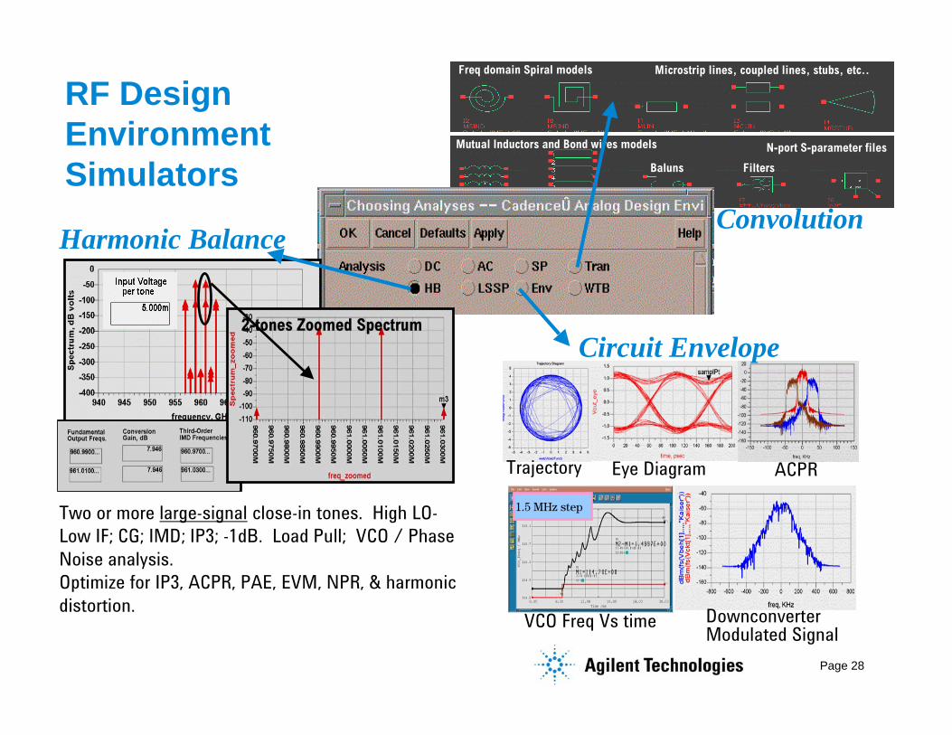
RF DesignEnvironmentSimulators
Freq domain Spiral models Microstrip lines, coupled lines, stubs, etc..
Mutual Inductors and Bond wires models
Baluns Filters
N-port S-parameter files
2-tones Zoomed Spectrum
Two or more large-signal close-in tones. High LO-Low IF; CG; IMD; IP3; -1dB. Load Pull; VCO / PhaseNoise analysis.Optimize for IP3, ACPR, PAE, EVM, NPR, & harmonicdistortion.
Trajectory Eye Diagram ACPR
1.5 MHz step
VCO Freq Vs time DownconverterModulated Signal
Harmonic Balance
Circuit Envelope
Convolution
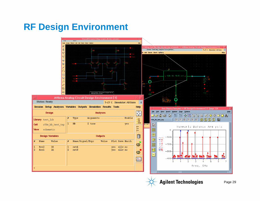
Page 29
RF Design Environment
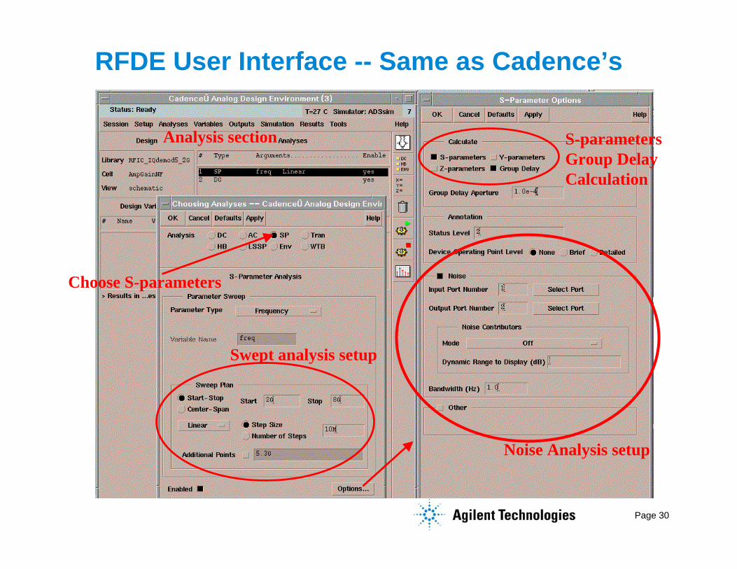
Page 30
RFDE User Interface -- Same as Cadence’s
Noise Analysis setup
Choose S-parameters
S-parametersGroup DelayCalculation
Swept analysis setup
Analysis section

Page 31
LNA schematic
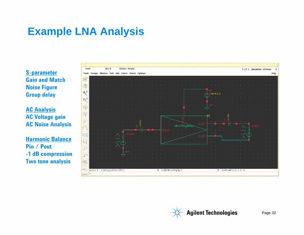
Page 32
Example LNA Analysis
S-parameterGain and MatchNoise FigureGroup delay
AC AnalysisAC Voltage gainAC Noise Analysis
Harmonic BalancePin / Pout-1 dB compressionTwo tone analysis
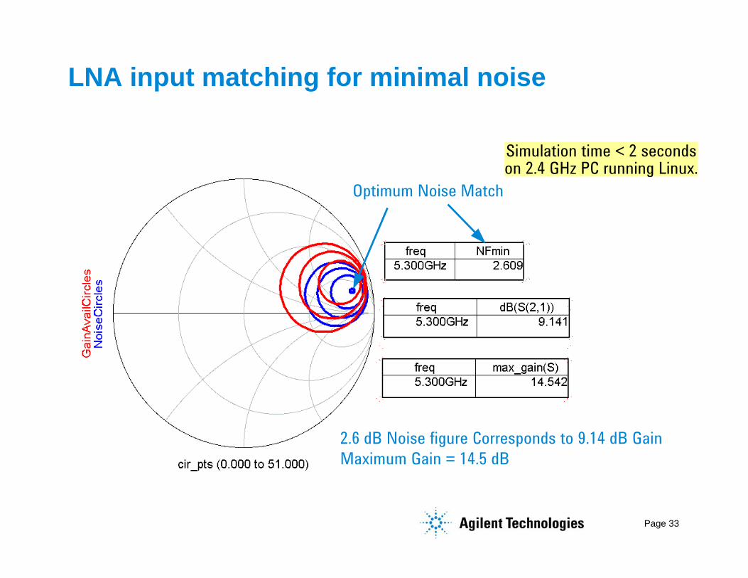
Page 33
LNA input matching for minimal noise
Optimum Noise Match
2.6 dB Noise figure Corresponds to 9.14 dB GainMaximum Gain = 14.5 dB
Simulation time < 2 secondson 2.4 GHz PC running Linux.
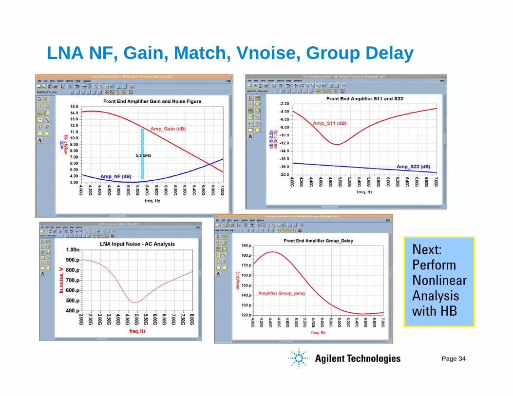
Page 34
LNA NF, Gain, Match, Vnoise, Group Delay
Next:PerformNonlinearAnalysiswith HB
Page 35
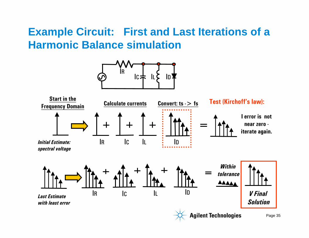
Example Circuit: First and Last Iterations of aHarmonic Balance simulation
I error is notnear zero -
iterate again.
IRIC IL ID
V Final Solution
Within tolerance
Test (Kirchoff’s law):
Last Estimatewith least error
IR IC IL ID
IDIR IC ILInitial Estimate:spectral voltage
Start in theFrequency Domain Convert: ts -> fsCalculate currents

Page 36
HB efficiency example
0.5 seconds 57 seconds
Page 37
Harmonic Balance benefits
• Provides steady-state solution of nonlinear circuits with multitoneexcitation.
• Handles multiple independent signals, no matter how closely spaced infrequency. (Signals need not be co-periodic)
• Dynamic range and accuracy of solution increases exponentially with #harmonics
• Able to easily and accurately include models described in thefrequency domain (e.g. packages, spiral inductors, etc.)
• Easily handles Nonlinear Noise, including Phase Noise• Voltages and currents are described and stored in frequency domain.
Benefits optimization of RF parameters and solution re-use.
Page 38
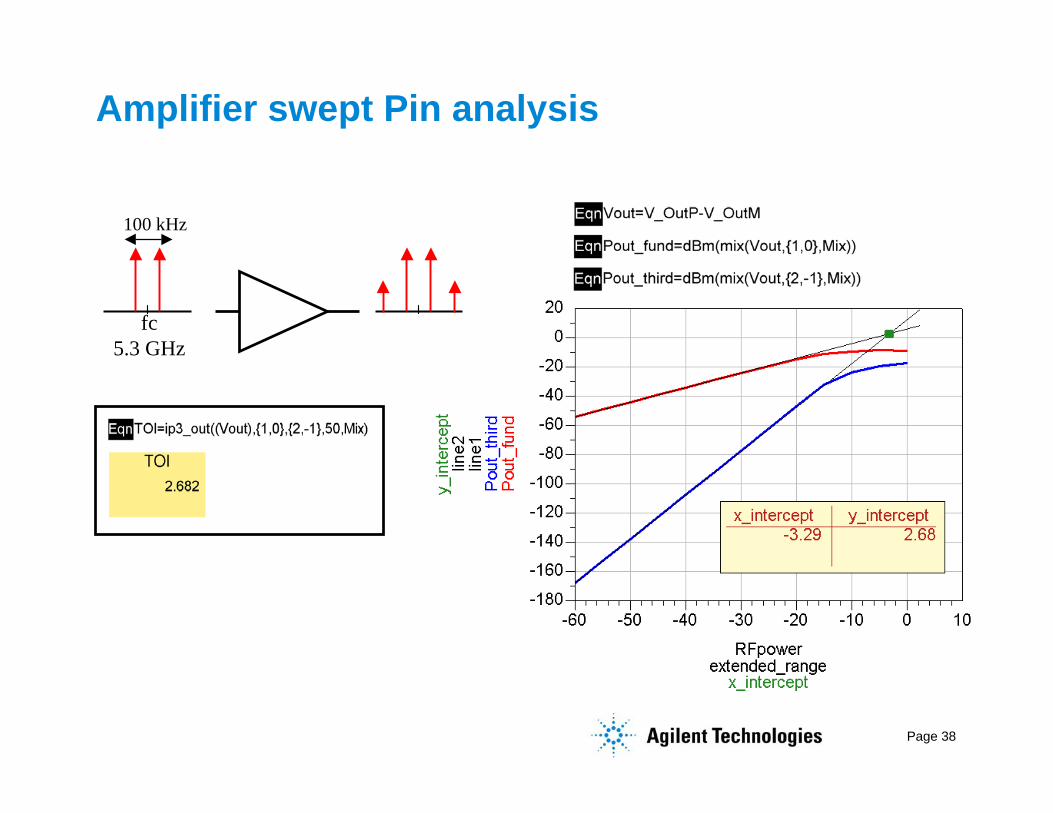
Amplifier swept Pin analysis
fc5.3 GHz
100 kHz
Page 39
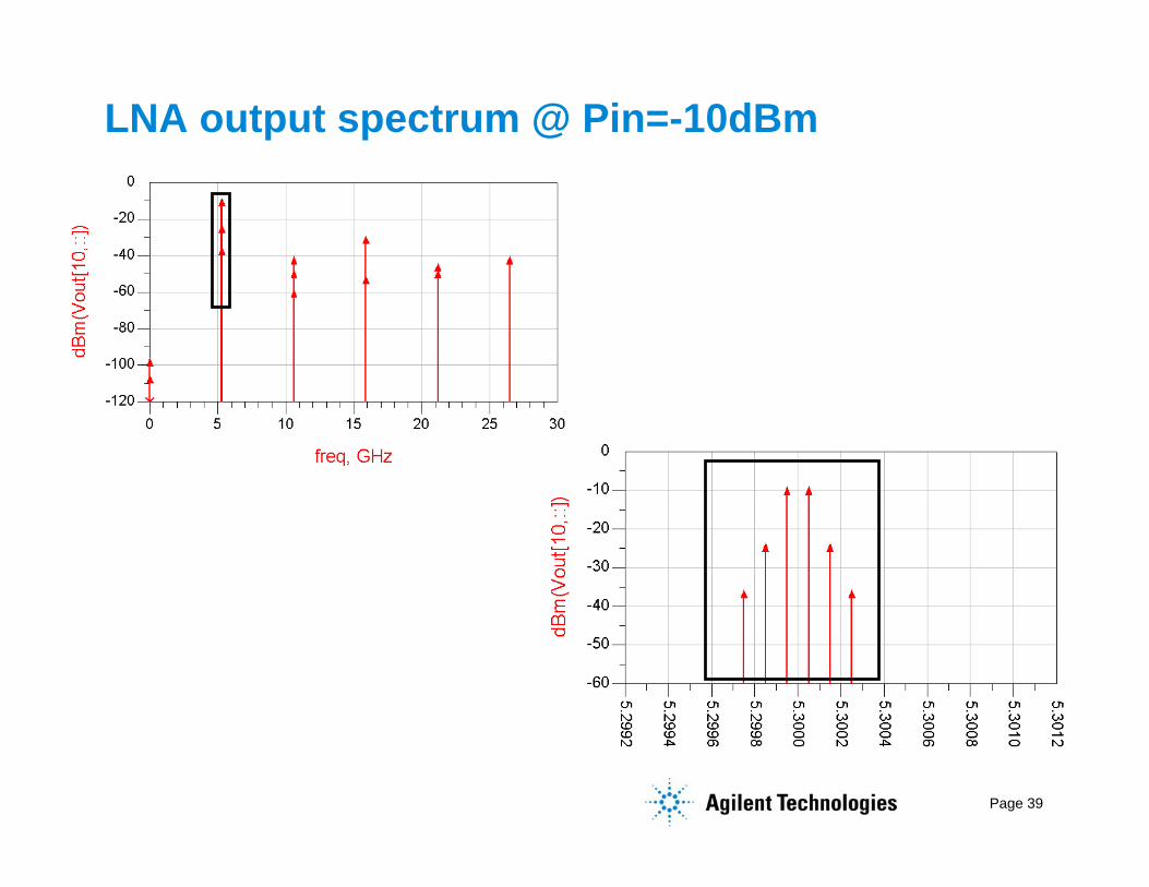
LNA output spectrum @ Pin=-10dBm
Page 40
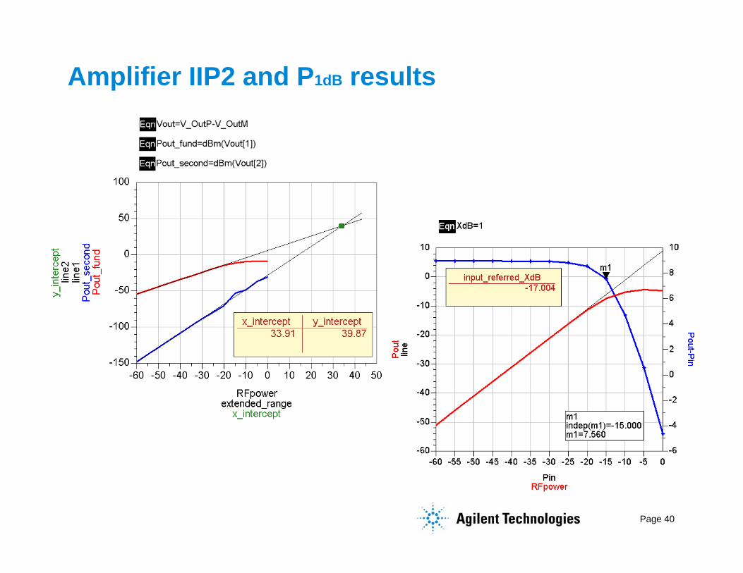
Amplifier IIP2 and P1dB results
Page 41
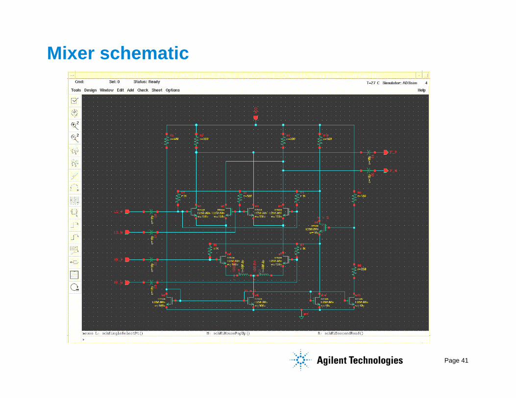
Mixer schematic
Page 42
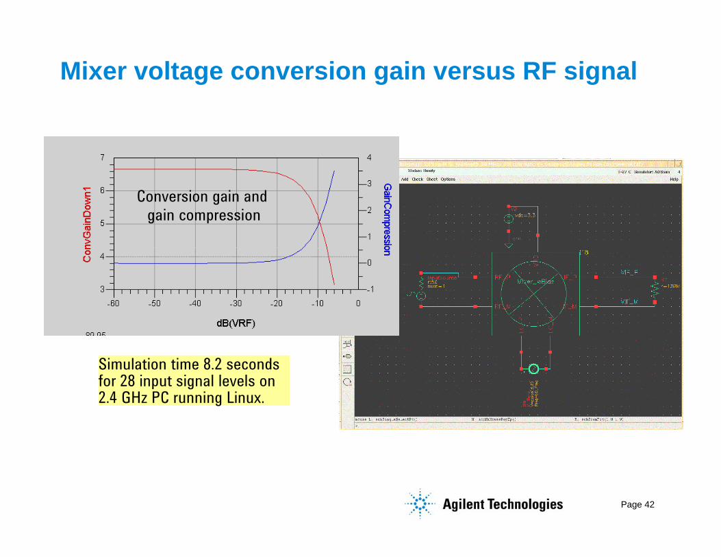
Mixer voltage conversion gain versus RF signal
Conversion gain and gain compression
Simulation time 8.2 secondsfor 28 input signal levels on2.4 GHz PC running Linux.
Page 43
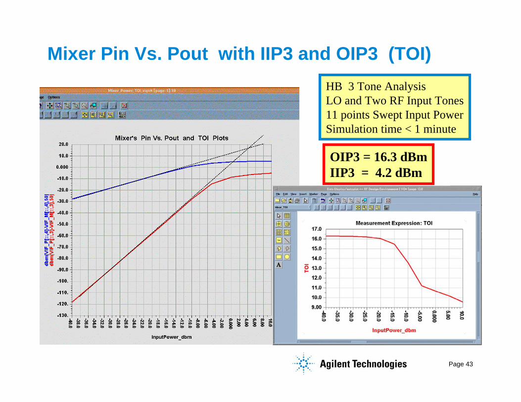
Mixer Pin Vs. Pout with IIP3 and OIP3 (TOI)HB 3 Tone AnalysisLO and Two RF Input Tones11 points Swept Input PowerSimulation time < 1 minute
OIP3 = 16.3 dBmIIP3 = 4.2 dBm
Page 44
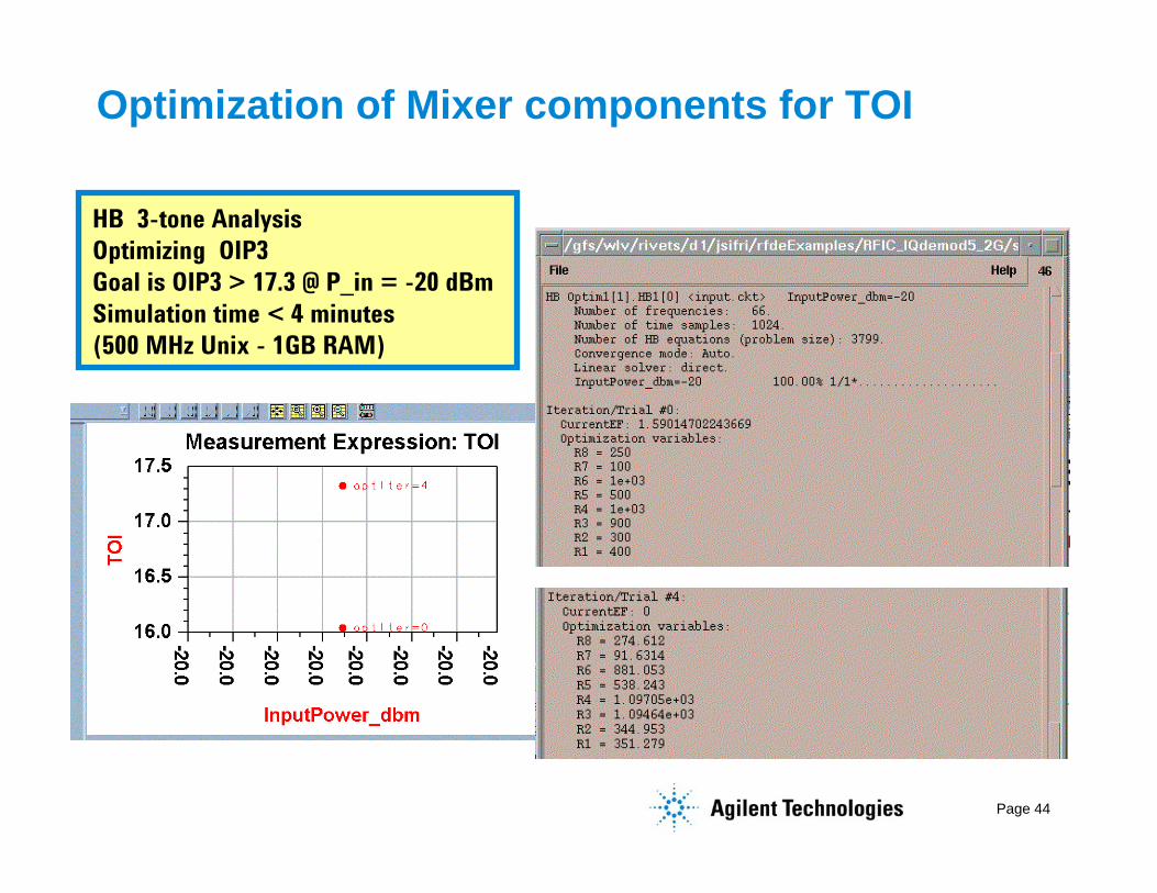
HB 3-tone AnalysisOptimizing OIP3Goal is OIP3 > 17.3 @ P_in = -20 dBmSimulation time < 4 minutes(500 MHz Unix - 1GB RAM)
Optimization of Mixer components for TOI
Page 45
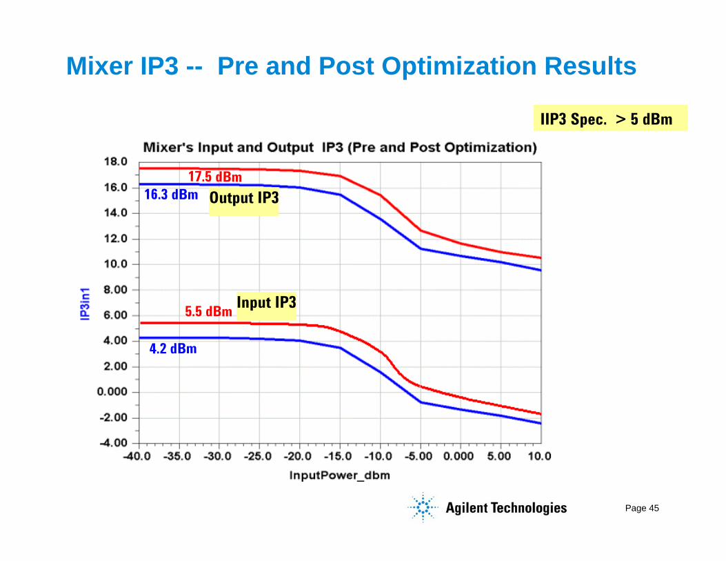
Mixer IP3 -- Pre and Post Optimization Results
4.2 dBm
16.3 dBm17.5 dBm
5.5 dBm
IIP3 Spec. > 5 dBm
Output IP3
Input IP3
Page 46
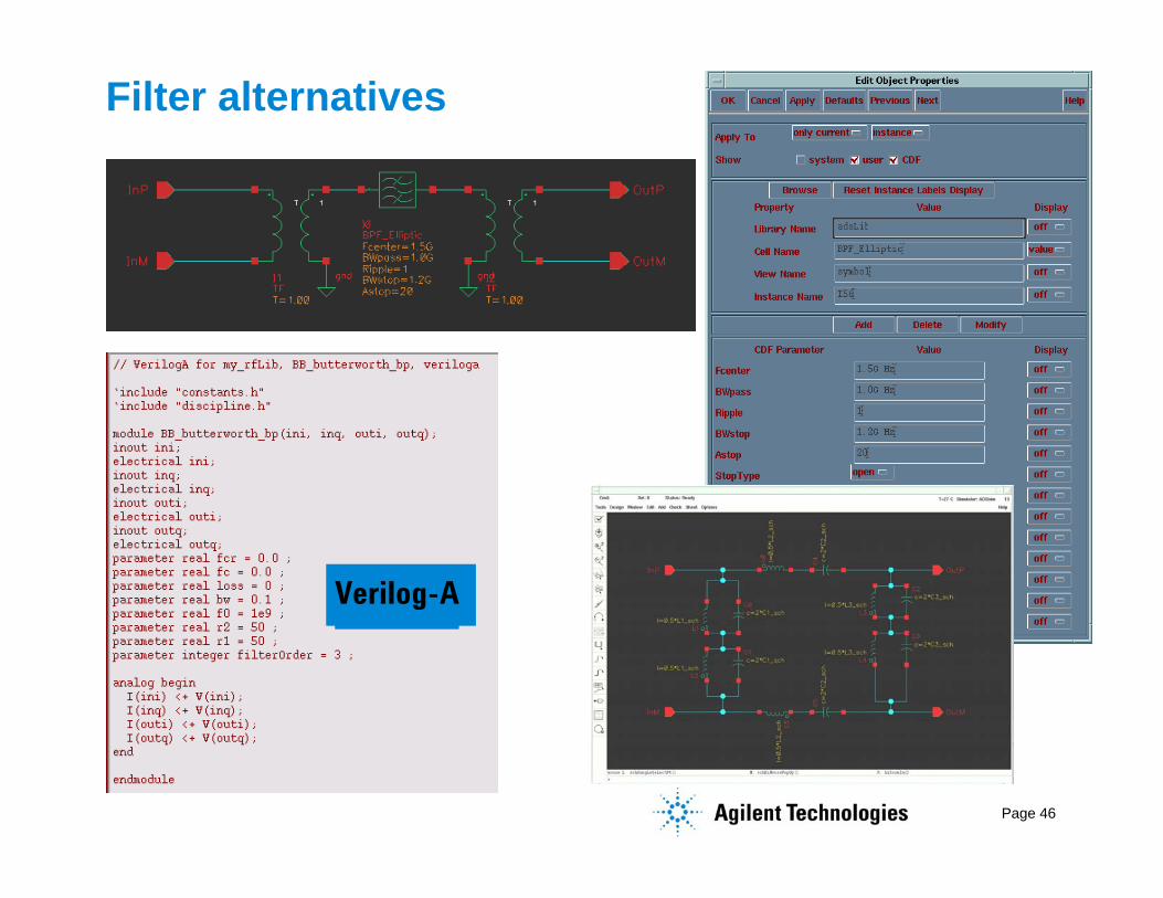
Filter alternatives
Verilog-A
Page 47
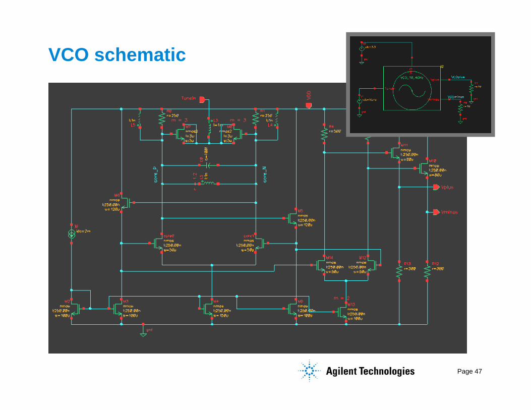
VCO schematic

Page 48
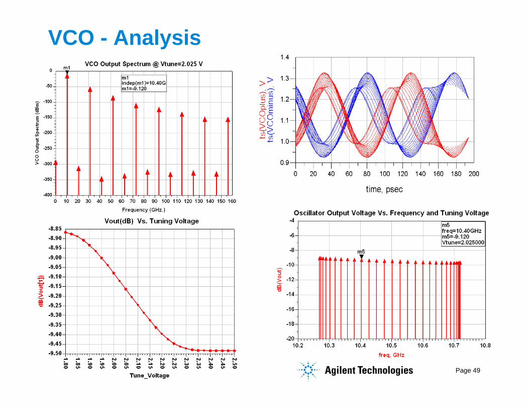
VCO AnalysisSimulation time 29.5 seconds for29 values of VCO tuning voltage,on 2.4 GHz PC running Linux.
Page 49
VCO - Analysis

Page 50
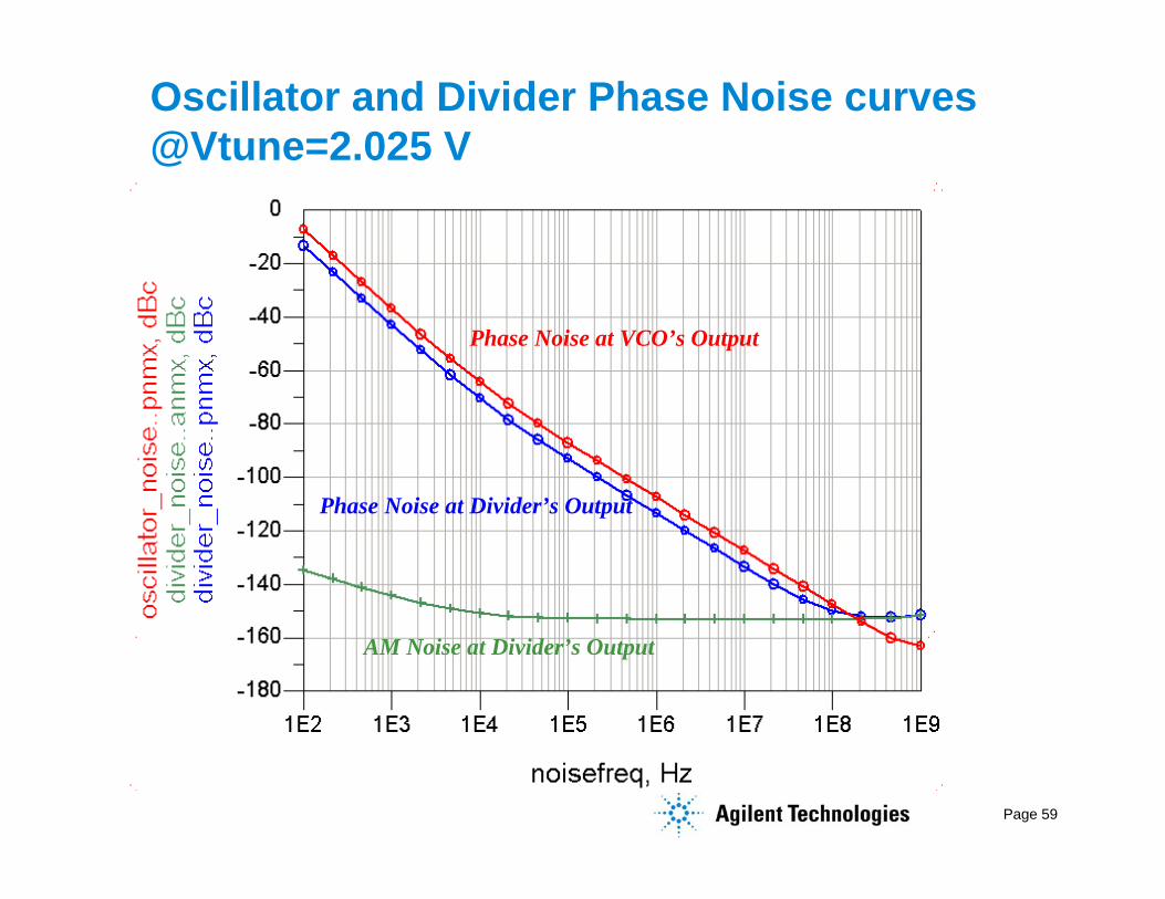
VCO - Phase Noise at Vtune = 2.025 volts

Page 51
Phase Noise contributors @ 100Hz and 10 MHz
Page 52
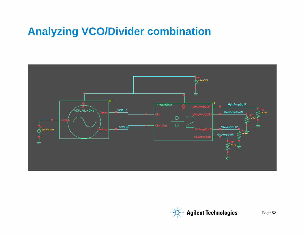
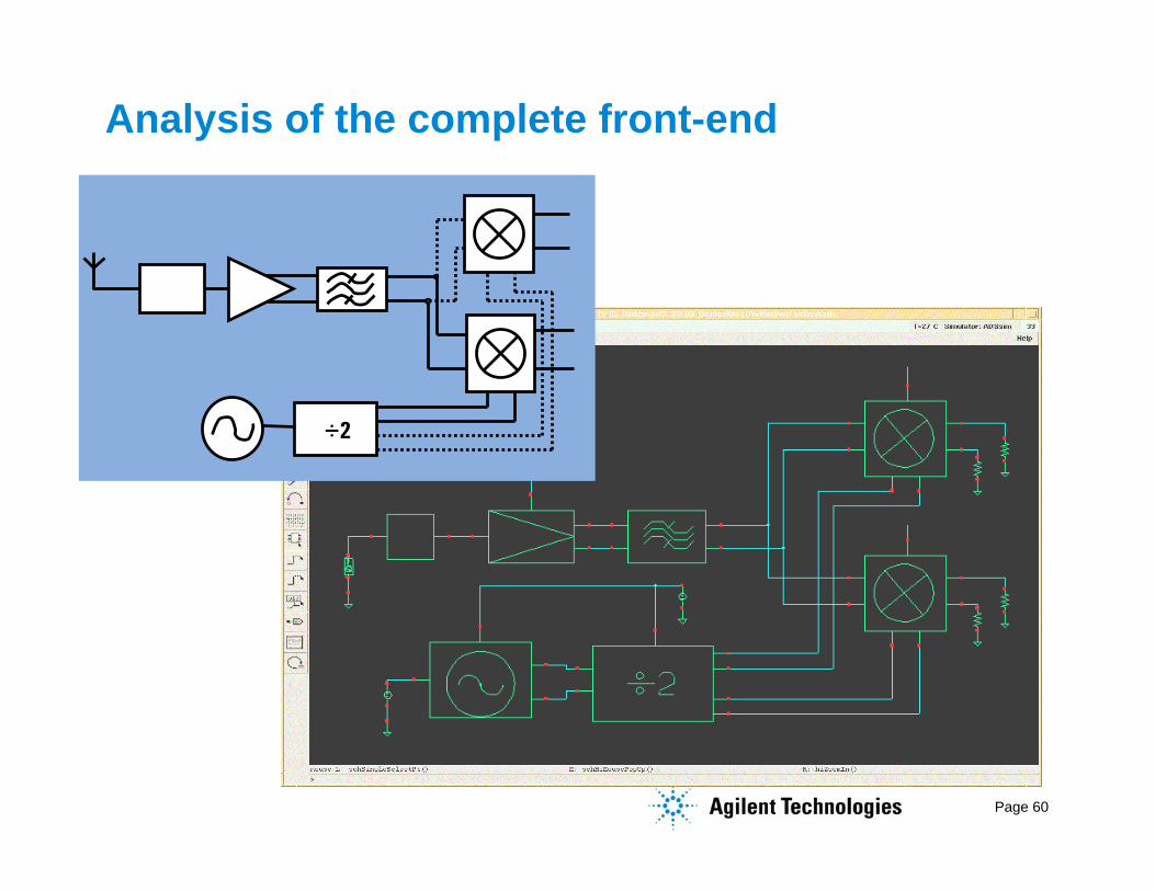
Analyzing VCO/Divider combination

Page 53
Divider schematic
Page 54
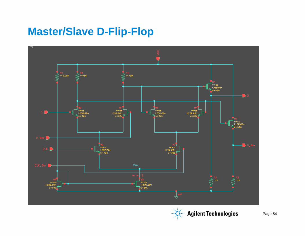
Master/Slave D-Flip-Flop

Page 55
Buffer Amp

Page 56
The need for Transient Assisted HarmonicBalance (TAHB)
Solution #1
Solution #2
DividerInput
Output
Output
HB Initial GuessSolution #1
Solution #2
Error tolerance circle

Page 57
VCO with trigger pulse source
Page 58
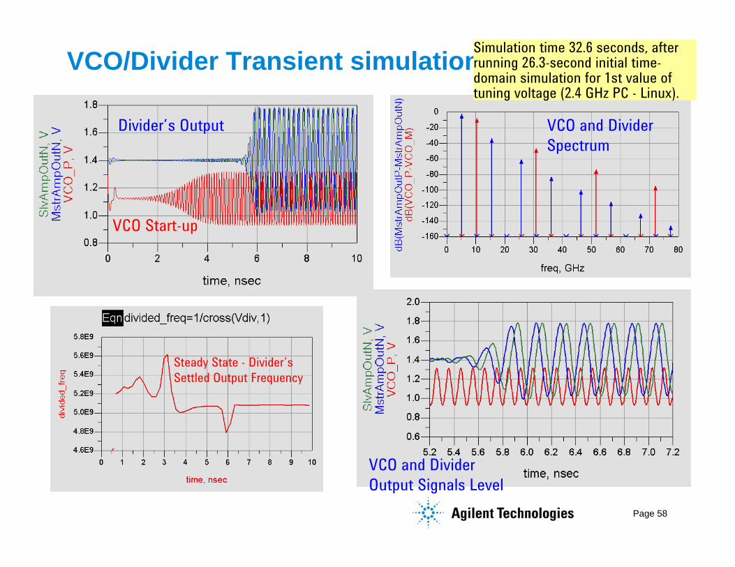
VCO/Divider Transient simulation
Divider’s Output
Steady State - Divider’sSettled Output Frequency
VCO and DividerOutput Signals Level
VCO and DividerSpectrum
VCO Start-up
Simulation time 32.6 seconds, afterrunning 26.3-second initial time-domain simulation for 1st value oftuning voltage (2.4 GHz PC - Linux).
Page 59
Oscillator and Divider Phase Noise curves@Vtune=2.025 V
Phase Noise at VCO’s Output
Phase Noise at Divider’s Output
AM Noise at Divider’s Output
Page 60
Analysis of the complete front-end
÷2
Page 61
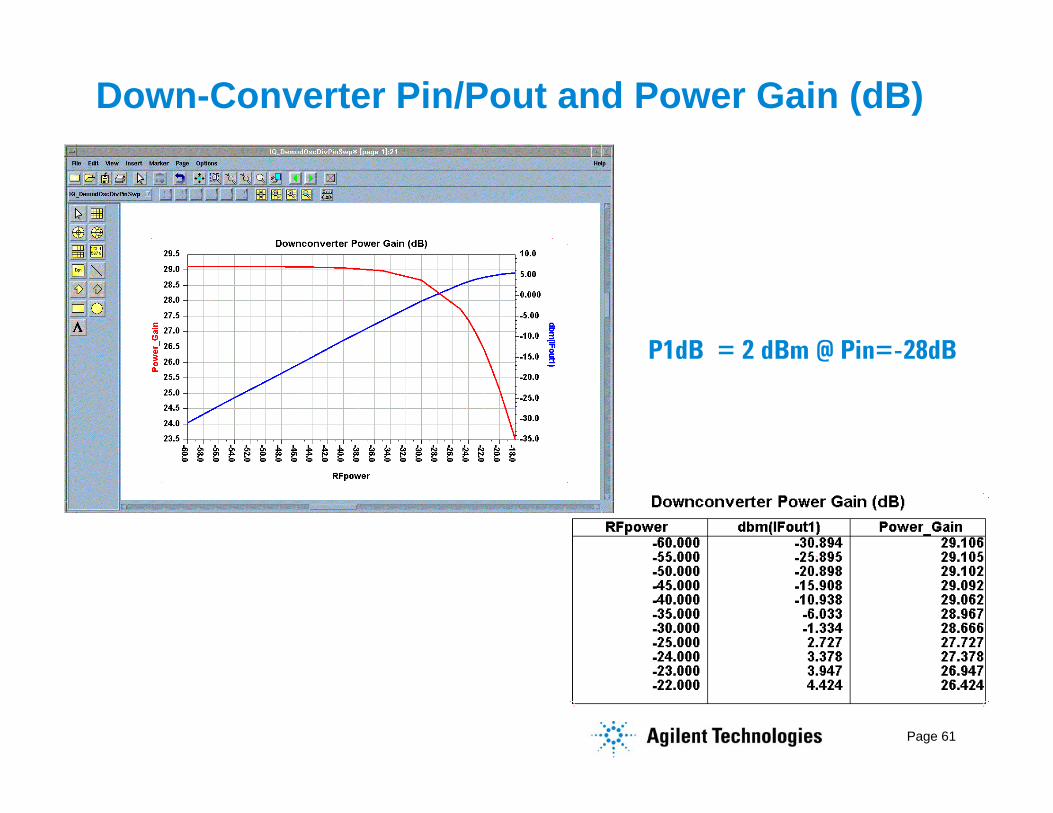
Down-Converter Pin/Pout and Power Gain (dB)
P1dB = 2 dBm @ Pin=-28dB
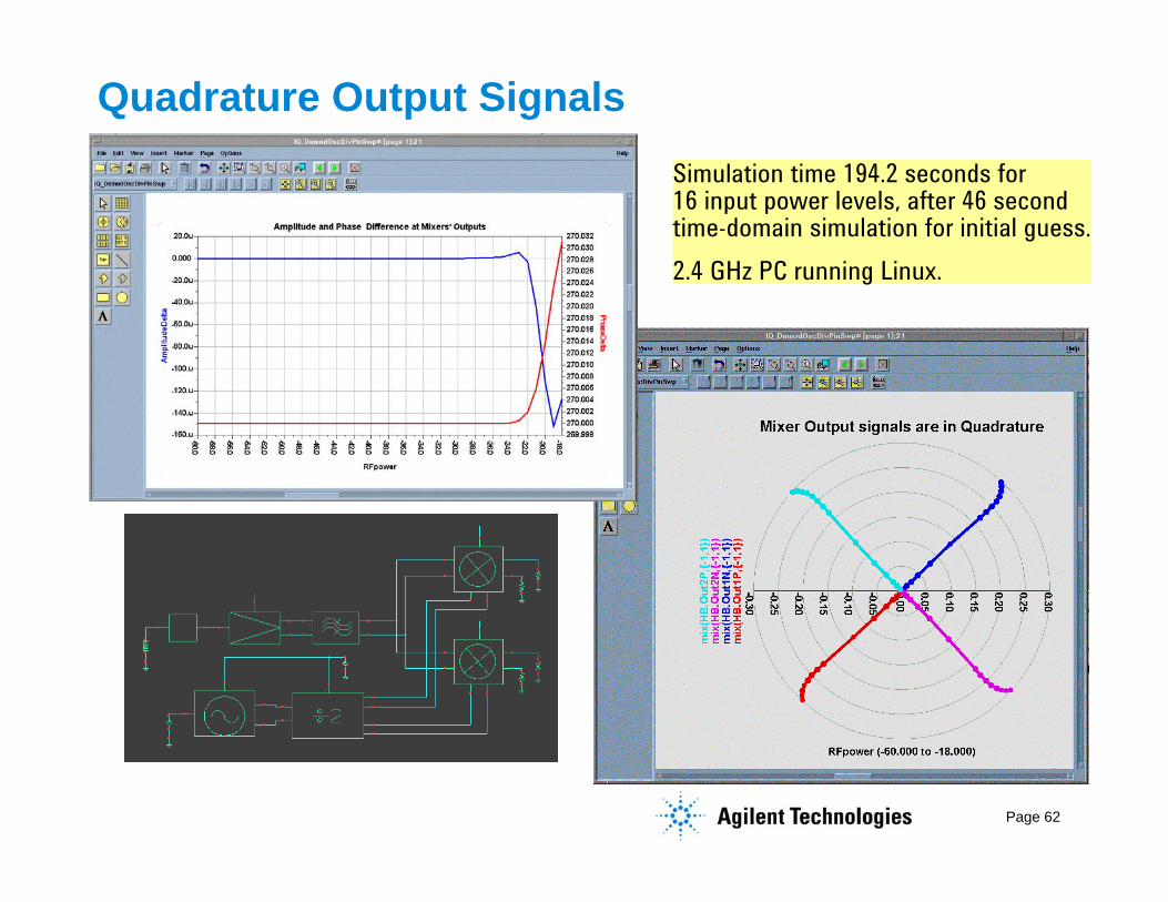
Page 62
Quadrature Output SignalsSimulation time 194.2 seconds for 16 input power levels, after 46 second time-domain simulation for initial guess.2.4 GHz PC running Linux.

Page 63
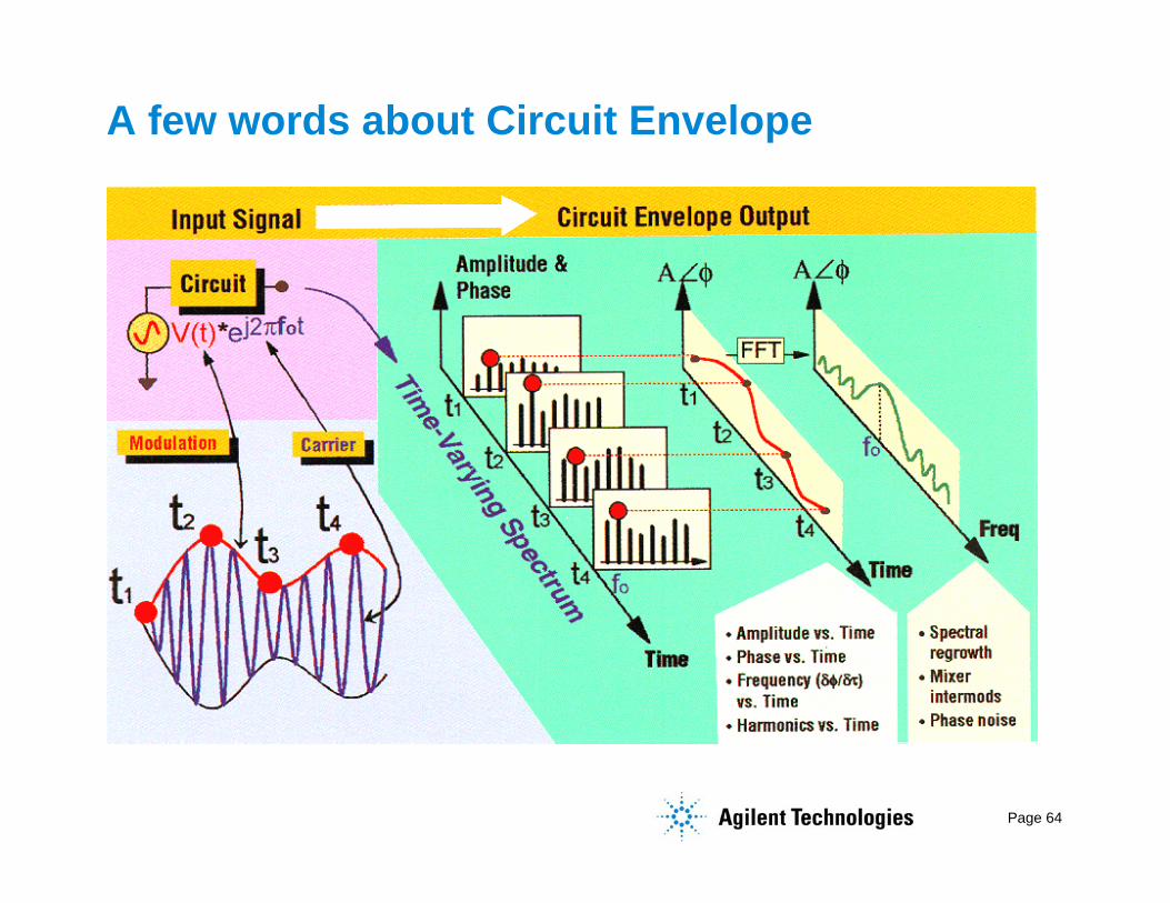
A few words about Circuit Envelope
• Complex waveforms need accurate representation in time andfrequency domain
• Signals are narrowband compared with frequency of operation
0.5/Tstepfc 2fc 3fc
Spectrum is99.99%empty
20 MHz
5 GHz
Page 64
A few words about Circuit Envelope
Page 65
Summary – Part 2
• Harmonic Balance and other frequency domain simulation toolswere used to simulate RF blocks of a receiver front-end.
• IMD and IP3 of two close in tones with high LO and Low IF.• Pin / Pout and Power Spectrum• Efficient Optimization for IP3• VCO / Divider phase Noise
• It was shown how Agilent's simulation technologies areintegrated in the Cadence IC design environment
• Next, we will combine these RF blocks into a system and verifythe design using Ptolemy, Circuit Envelope, and RFDE’s newWireless Test Benches (WTB).
Page 66
Agenda
System Definition
SystemVerification
Circuit/RFICDesign & Verification
SystemIntegration
Baseband
Tape-out
EM
pre/post-tapeout• Introduction• Part 1: System Design & Specification
• Transmitter• Receiver
• Part 2: Circuit Simulation & Analysis• Part 3: Verification of Circuit Design to
System Specifications• Transmitter• Receiver• Final Verification
Page 67
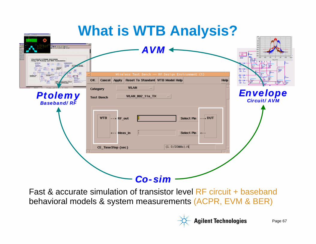
What is WTB Analysis?
PtolemyPtolemyBaseband/RFBaseband/RF
Co-simCo-simFast & accurate simulation of transistor level RF circuit + basebandbehavioral models & system measurements (ACPR, EVM & BER)
EnvelopeEnvelopeCircuit/AVMCircuit/AVM
AVMAVM

Page 68
Verify RFIC Design with digitally modulated signals on circuit pageUsing Envelope Simulator
Sources & Expressions
Optimize modulated measurementsperformance (ACPR, EVM, ..) of circuitdesign with circuit parameters
WLAN 802.11a
Ptolemy PtolemyModulatedModulated
DSP SourcesDSP Sources
fc 2fc 3fc
Spectrum is99.99%empty
20 MHz
5 GHz
Page 69
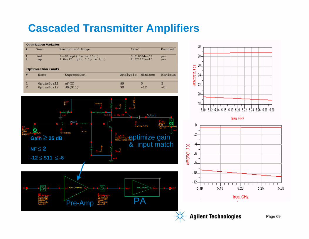
Cascaded Transmitter Amplifiers
optimize gain& input match
Gain ≥ 25 dB
NF ≤ 2-12 ≤ S11 ≤ -8
pre/post-tapeout
PAPre-Amp
Page 70
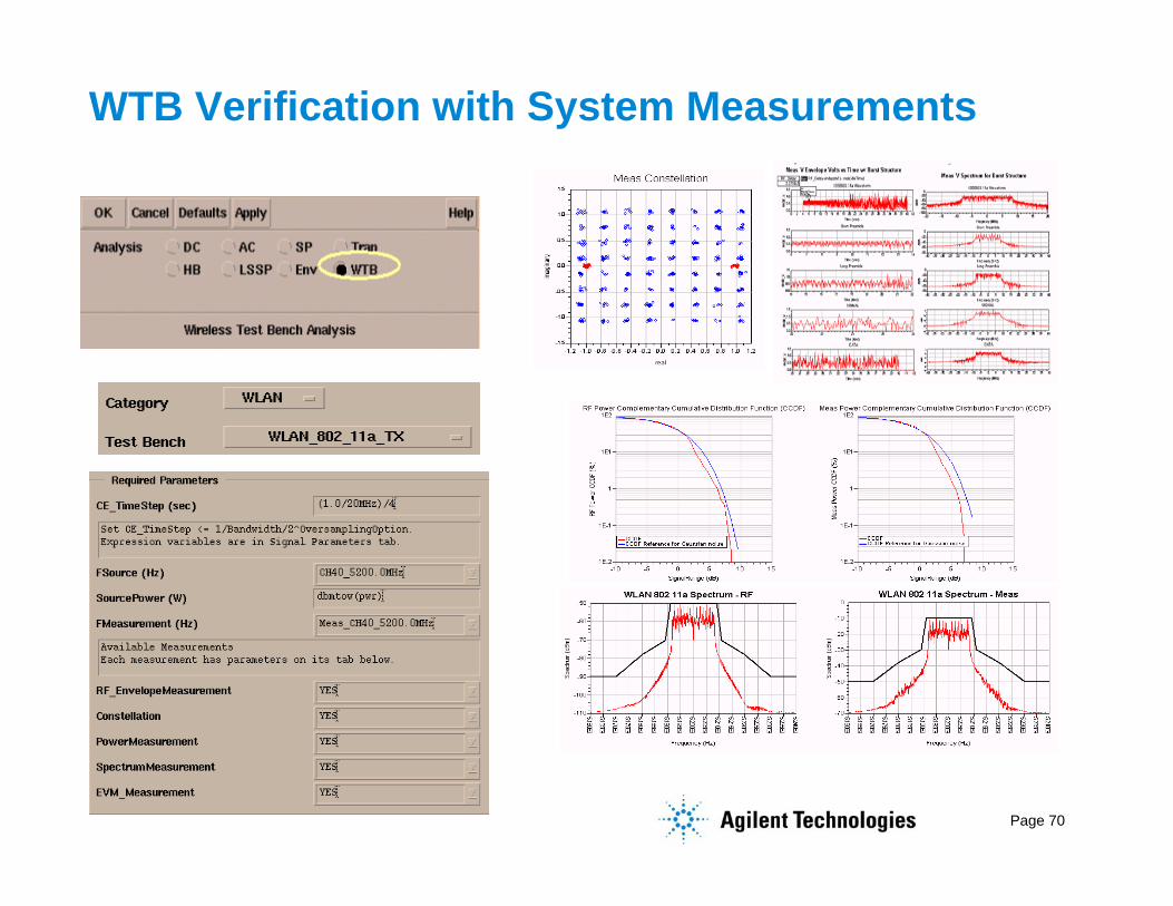
WTB Verification with System Measurements
Page 71
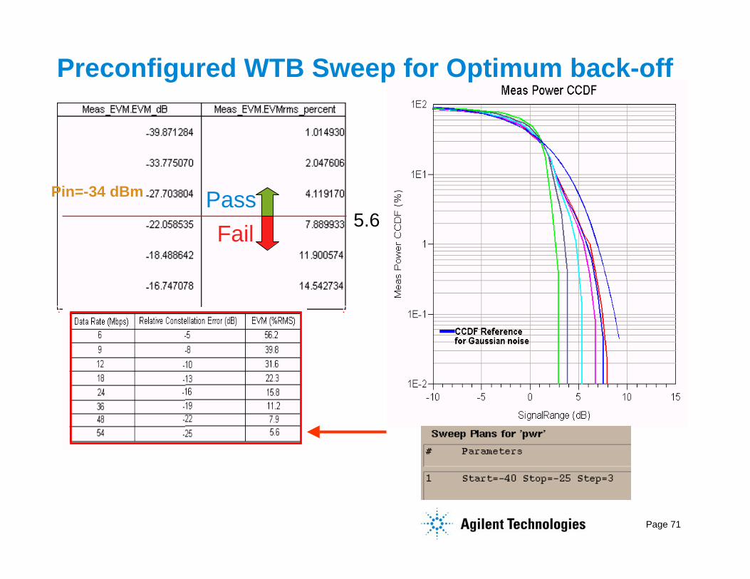
Preconfigured WTB Sweep for Optimum back-off
Pin=-34 dBm PassFail 5.6
Page 72
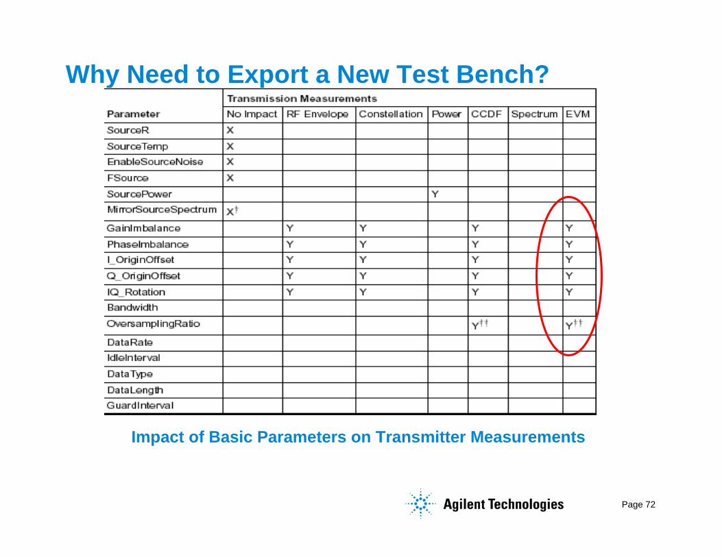
Why Need to Export a New Test Bench?
Impact of Basic Parameters on Transmitter Measurements

Page 73
Exporting Wireless Test Bench to RFDE• Modify a template design
• Leave circuit out with ports
• Place desired measurements
• Verify before export
• Export
34
1
2
5
pre/post-tapeout

Page 74
Updated Wireless Test Bench
New Parameter
The new test bench includes Oscillator PN as a new option
Constellation distortion due to PN
Page 75
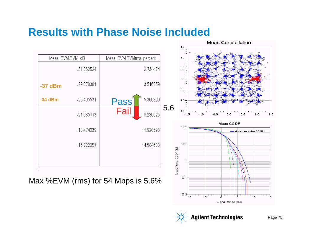
Results with Phase Noise Included
-37 dBm
-34 dBm PassFail
Max %EVM (rms) for 54 Mbps is 5.6%
5.6
Page 76
Agenda
• Introduction• Part 1: System Design & Specification
• Transmitter• Receiver
• Part 2: Circuit Simulation & Analysis• Part 3: Verification of Circuit Design to
System Specifications• Transmitter• Receiver• Final Verification
Page 77
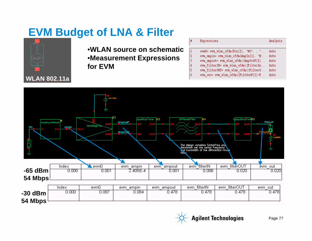
EVM Budget of LNA & Filter
-65 dBm54 Mbps
-30 dBm54 Mbps
•WLAN source on schematic•Measurement Expressionsfor EVM
WLAN 802.11a
Page 78
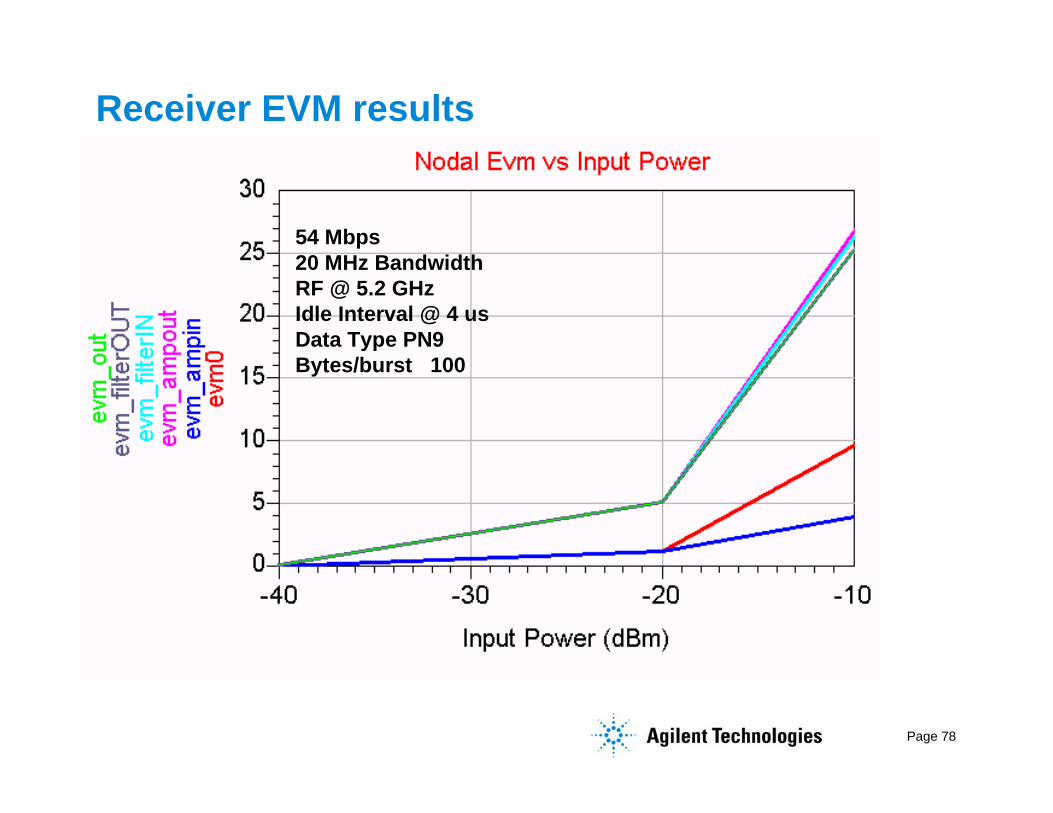
Receiver EVM results
54 Mbps20 MHz BandwidthRF @ 5.2 GHzIdle Interval @ 4 usData Type PN9Bytes/burst 100

Page 79
DUT & Custom Test Bench
Page 80
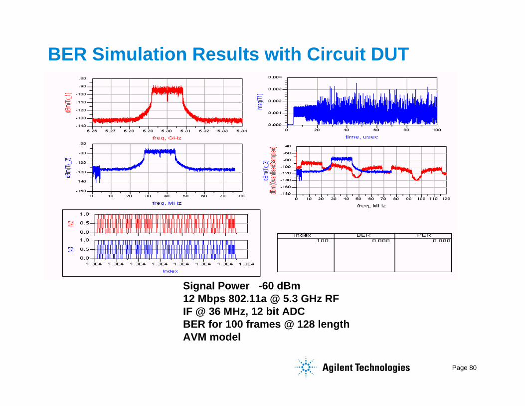
BER Simulation Results with Circuit DUT
Signal Power -60 dBm12 Mbps 802.11a @ 5.3 GHz RFIF @ 36 MHz, 12 bit ADCBER for 100 frames @ 128 lengthAVM model

Page 81
More Receiver Sensitivity Results
Signal Power Variable12 Mbps 802.11a @ 5.3 GHz RFIF @ 36 MHz, 12 bit ADCBER for 100 frames @ 128 length
Page 82
Agenda
SystemDefinition
Verification
Circuit/RFICDesign & Verification
SystemIntegration
Baseband
Tape-out
EM
pre/post-tapeout
• Introduction• Part 1: System Design & Specification
• Transmitter• Receiver
• Part 2: Circuit Simulation & Analysis• Part 3: Verification of Circuit Design to
System Specifications• Transmitter• Receiver• Final Verification
Page 83
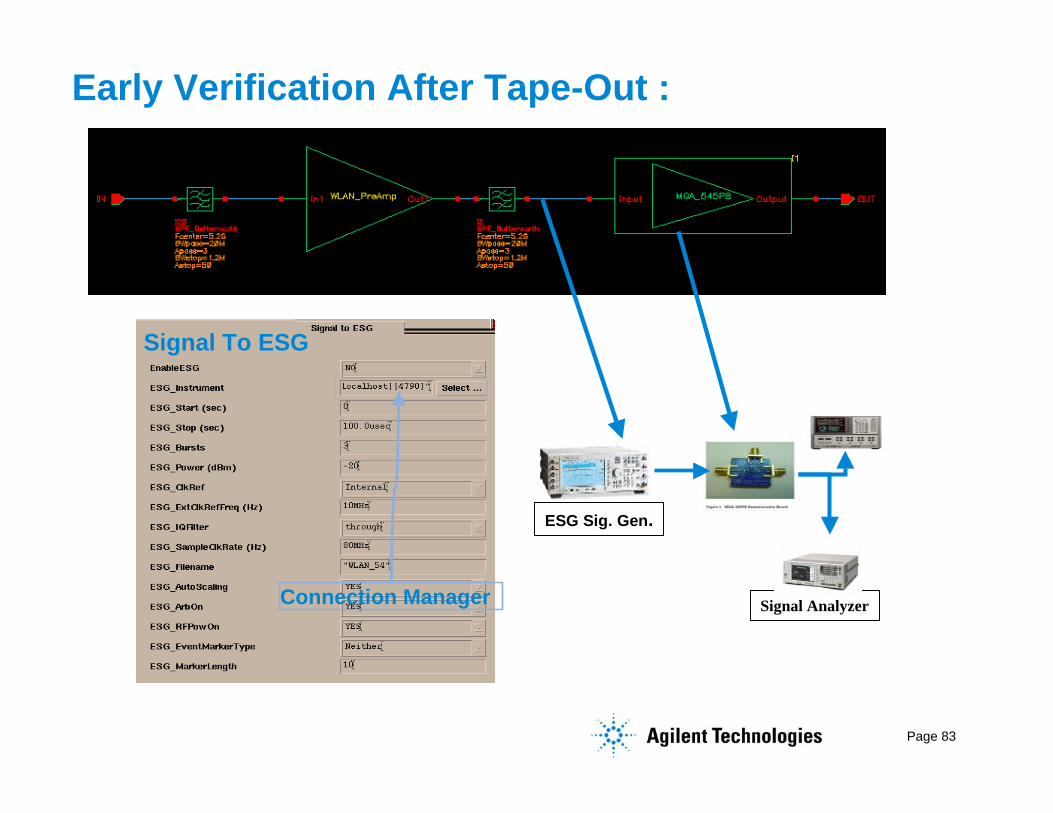
Early Verification After Tape-Out :
ESG Sig. Gen.
Signal Analyzer
Signal To ESG
Connection Manager
Page 84
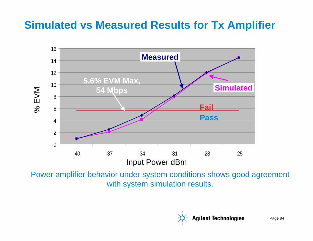
Simulated vs Measured Results for Tx Amplifier
0
2
4
6
8
10
12
14
16
-40 -37 -34 -31 -28 -25
FailPass
5.6% EVM Max,54 Mbps
% E
VM
Input Power dBmPower amplifier behavior under system conditions shows good agreement
with system simulation results.
Simulated
Measured
Page 85
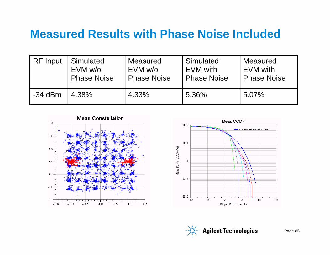
Measured Results with Phase Noise Included
5.07%5.36%4.33%4.38%-34 dBm
MeasuredEVM withPhase Noise
SimulatedEVM withPhase Noise
MeasuredEVM w/oPhase Noise
SimulatedEVM w/oPhase Noise
RF Input
Page 86
Summary• System definition, circuit design, integration and
verification stages are indispensable stages ofwireless product generation
• The optimum flow would allow system and circuitdesigners to communicate seamlessly in their ownhome base
• ADS is the platform of choice for system definition• The RFDE is the platform for full RFIC design &
implementation• Wireless Test bench provides ADS system baseband
capabilities to RFDE for a complete flow• A WLAN transmitter case study utilizing this flow was
described