week 11: chap. 16b pulse shaping - michigan state university · pulse processing: timing-filter amp...
TRANSCRIPT
Week 11: Chap. 16b Pulse Shaping
© DJMorrissey, 2o17
Pulse Processing (passive)
Pulse Shaping (active)-- Op Amps-- CR/RC network-- Bipolar pulses--- Shaping network--- Pole Zero network--- Baseline Restorer-- Delay-line clipping
Pulse Processing & Noise
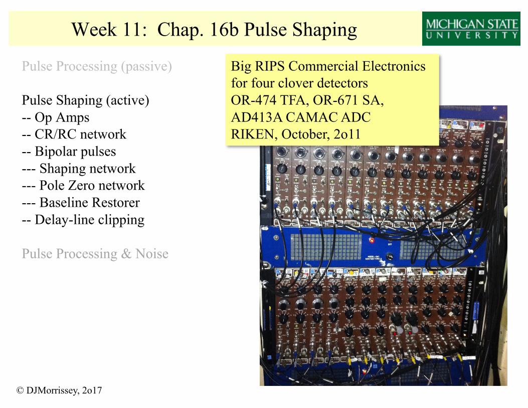
Big RIPS Commercial Electronics for four clover detectors OR-474 TFA, OR-671 SA, AD413A CAMAC ADC RIKEN, October, 2o11
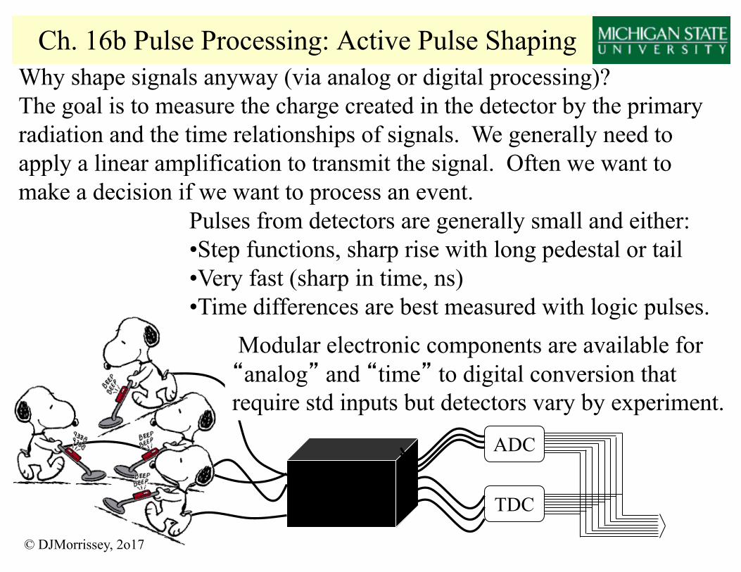
Pulses from detectors are generally small and either:•Step functions, sharp rise with long pedestal or tail •Very fast (sharp in time, ns) •Time differences are best measured with logic pulses.
© DJMorrissey, 2o17
Ch. 16b Pulse Processing: Active Pulse ShapingWhy shape signals anyway (via analog or digital processing)? The goal is to measure the charge created in the detector by the primary radiation and the time relationships of signals. We generally need to apply a linear amplification to transmit the signal. Often we want to make a decision if we want to process an event.
ADC
TDC
Modular electronic components are available for “analog” and “time” to digital conversion that require std inputs but detectors vary by experiment.
Pulse Shapes, for example
© DJMorrissey, 2o17
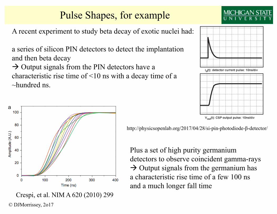
A recent experiment to study beta decay of exotic nuclei had:
a series of silicon PIN detectors to detect the implantation and then beta decay à Output signals from the PIN detectors have a characteristic rise time of <10 ns with a decay time of a ~hundred ns.
Crespi, et al. NIM A 620 (2010) 299
Plus a set of high purity germanium detectors to observe coincident gamma-raysà Output signals from the germanium has a characteristic rise time of a few 100 ns and a much longer fall time
http://physicsopenlab.org/2017/04/28/si-pin-photodiode-β-detector/
© DJMorrissey, 2o17
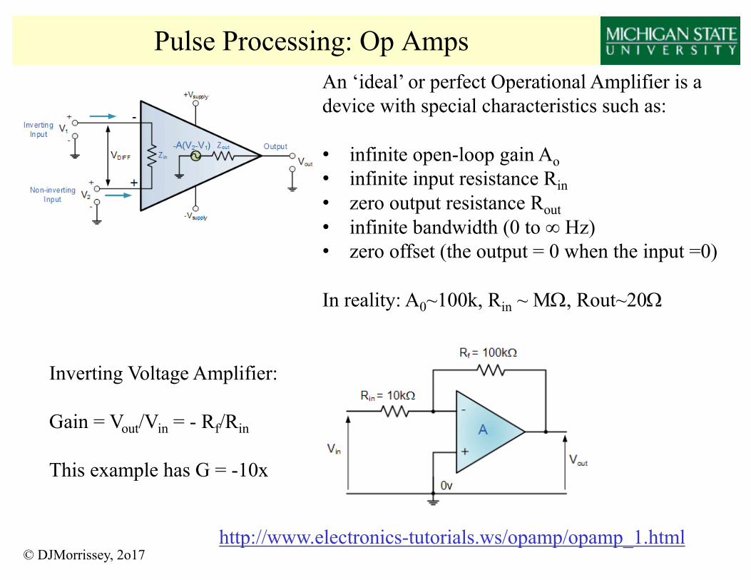
Pulse Processing: Op AmpsAn ‘ideal’ or perfect Operational Amplifier is a device with special characteristics such as:
• infinite open-loop gain Ao• infinite input resistance Rin• zero output resistance Rout• infinite bandwidth (0 to ∞ Hz) • zero offset (the output = 0 when the input =0)
In reality: A0~100k, Rin ~ MW, Rout~20W
http://www.electronics-tutorials.ws/opamp/opamp_1.html
Inverting Voltage Amplifier:
Gain = Vout/Vin = - Rf/Rin
This example has G = -10x

© DJMorrissey, 2o17
Pulse Processing: CR-RC shaperFig. 16.11 Knoll, 3rd Ed., 17.4 4th Ed.
Fig. 16.12 Knoll, 3rd Ed.
17.5 4th Ed.
€
Vout =Vinτ1
τ1 − τ 2
$
% &
'
( ) e−t /τ1 − e− t /τ 2( )
Vout =Vintτ
$
% & '
( ) e− t /τ for τ int = τ dif = τ
The detector output is a “step function” and we would like to convert this into a short “pulse.” Recall the effect of a poor quality cable on a step function signal: integration.t1 t2
In
Hi-passLow-pass
Cf. Problem 16.11In Knoll, 3rd Ed.
17.4 in 4th Ed.
© DJMorrissey, 2o17
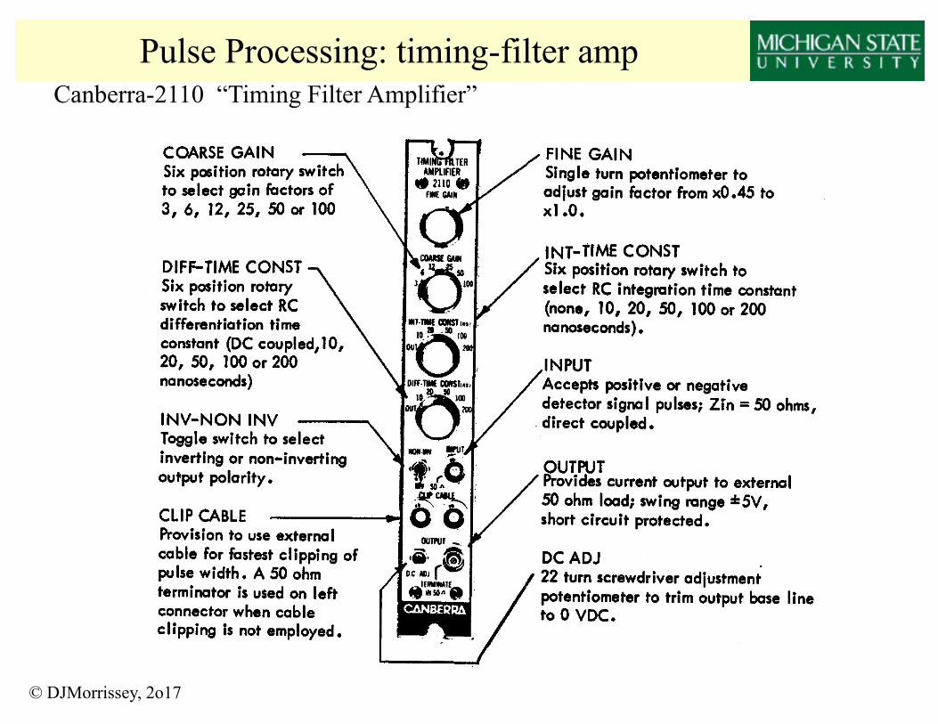
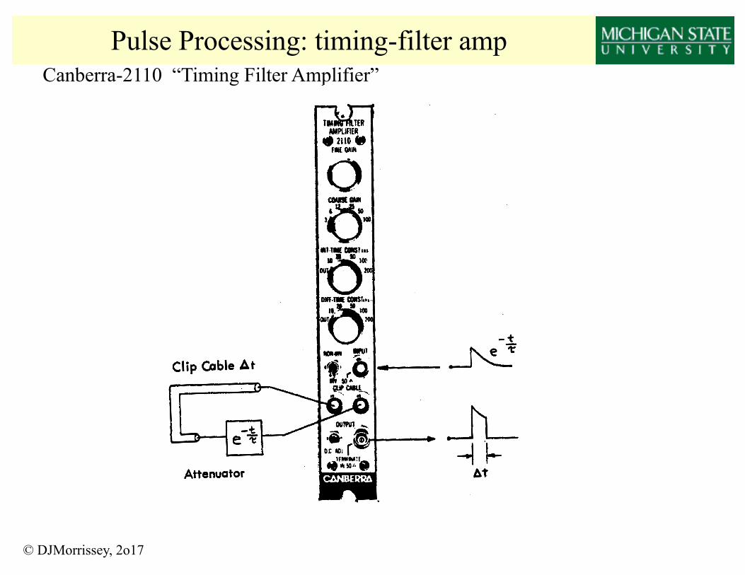
Pulse Processing: timing-filter ampCanberra-2110 “Timing Filter Amplifier”
© DJMorrissey, 2o17
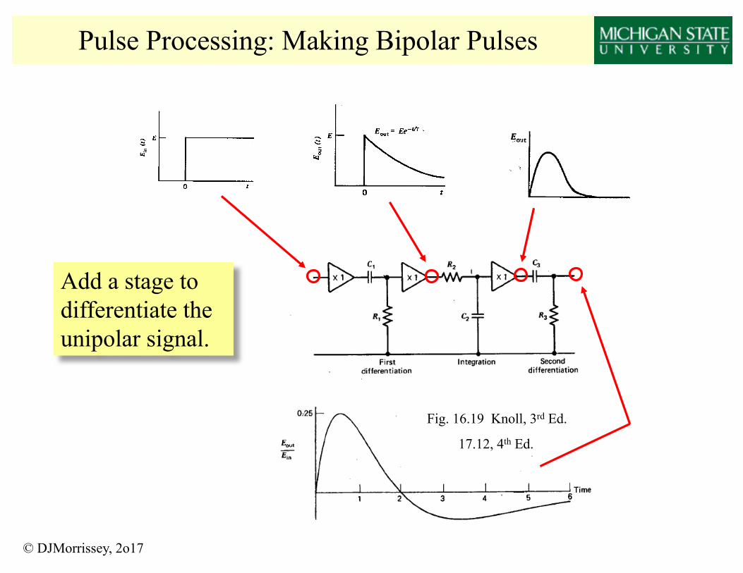
Pulse Processing: Making Bipolar Pulses
Fig. 16.19 Knoll, 3rd Ed.
17.12, 4th Ed.
Add a stage to differentiate the unipolar signal.
© DJMorrissey, 2o17
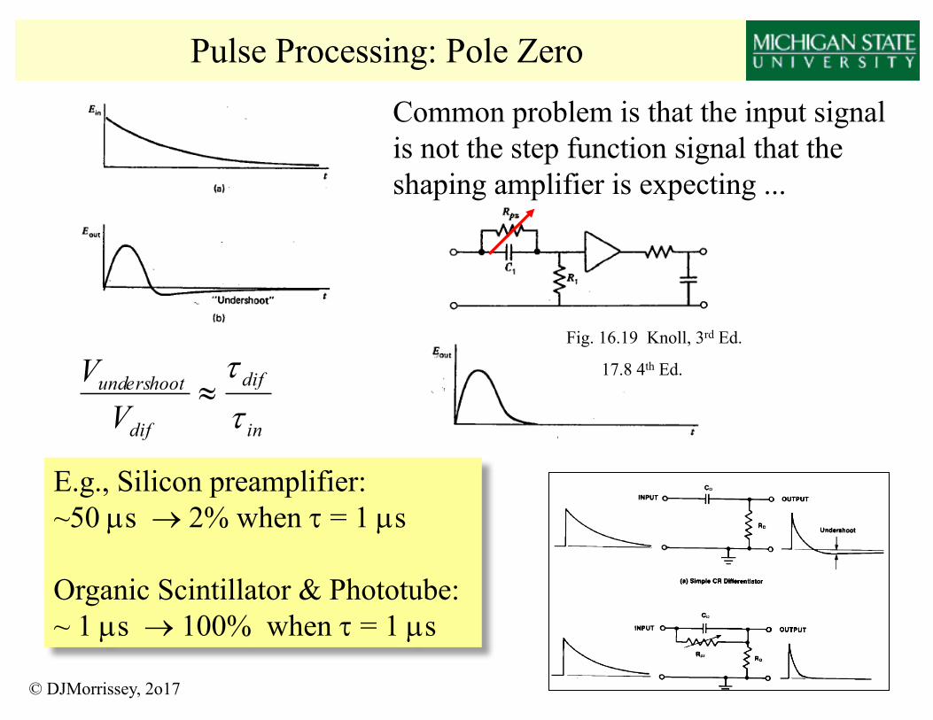
Pulse Processing: Pole Zero
Fig. 16.19 Knoll, 3rd Ed.
17.8 4th Ed.
Common problem is that the input signal is not the step function signal that the shaping amplifier is expecting ...
in
dif
dif
undershoot
VV
tt
»
E.g., Silicon preamplifier:~50 µs ® 2% when t = 1 µs
Organic Scintillator & Phototube:~ 1 µs ® 100% when t = 1 µs
© DJMorrissey, 2o17
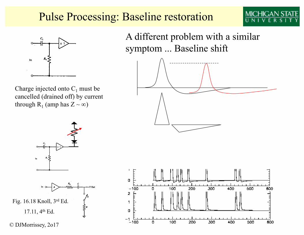
Pulse Processing: Baseline restoration
Fig. 16.18 Knoll, 3rd Ed.
17.11, 4th Ed.
A different problem with a similar symptom ... Baseline shift
Charge injected onto C1 must be cancelled (drained off) by current through R1 (amp has Z ~ ¥)
© DJMorrissey, 2o17
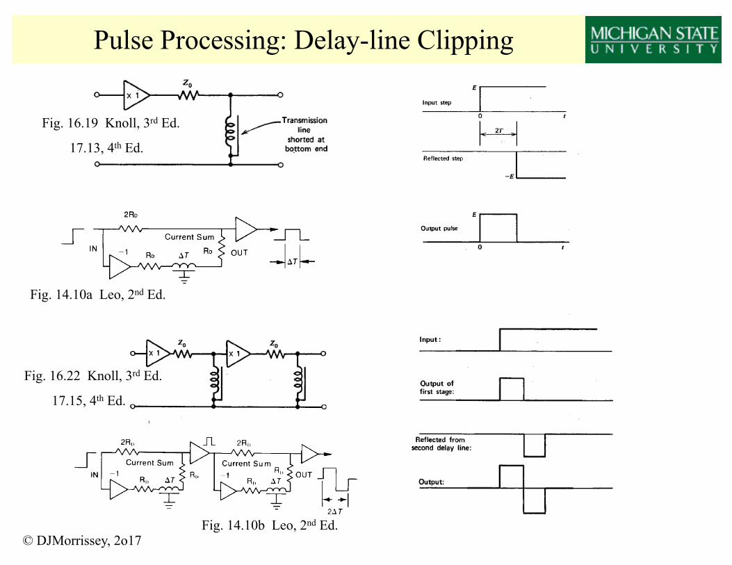
Pulse Processing: Delay-line Clipping
Fig. 16.19 Knoll, 3rd Ed.
17.13, 4th Ed.
Fig. 16.22 Knoll, 3rd Ed.
17.15, 4th Ed.
Fig. 14.10b Leo, 2nd Ed.
Fig. 14.10a Leo, 2nd Ed.
© DJMorrissey, 2o17
Pulse Processing: timing-filter ampCanberra-2110 “Timing Filter Amplifier”
© DJMorrissey, 2o17
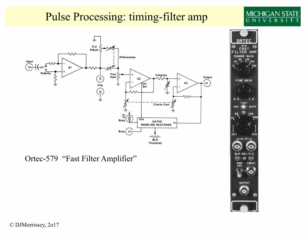
Pulse Processing: timing-filter amp
Ortec-579 “Fast Filter Amplifier”
The ORTEC Model 579 wideband Fast-Filter Amplifier with gated baselinerestorer (Fig. 1) enhances fast-timingmeasurements by improving the noise-to-slope ratio and providing ultra-high countrate spectroscopy capability.
A fast rise time (<8 ns), high output drive(±5 V into 50 Ω), and wide voltage gainrange (X0.9–X500) make the Model 579useful for many timing applications,including those utilizing low-gainphotomultiplier tubes. The Model 579 isparticularly suited for use with ORTECConstant-Fraction Discriminators such asModels 583, 935, or 473A in timingapplications with high-purity germanium(HPGe) or silicon charged-particledetectors (Figs. 2 and 9 and Tables 1 and2). Excellent dc and gain stability (±50µV/°C and ±0.05%/°C, respectively)eliminate the need for a dc leveladjustment. A Busy LED and BusyOutput are included to aid in BLRadjustment and system interfacing.
In addition, the wideband gated baselinerestorer and pole-zero cancellationnetwork permit ultra-high output countingrates. A wide variety of pulse filtering isavailable for improved signal processing.The Model 579 combines continuouslyvariable gain, independently selectableintegration and differentiation timeconstants (Out, 10, 20, 50, 100, 200, and500 ns), and cable clipping capability(external cable delay), making thisversatile unit an important asset forsophisticated time and energyspectroscopy.
579Fast-Filter Amplifier
ORTEC
• For fast timing with germanium and other semiconductor detectors
• Fast <8-ns rise time
• Independent integration and differentiation
• Gated baseline restorer
• Pole-zero cancellation
• 50-ΩΩ delay cable clipping
• Voltage gain X0.9 to X500
• Output drives to ±5 V on a 50-ΩΩ load
®
Fig. 1. Block Diagram of the Model 579 Fast-Filter Amplifier.
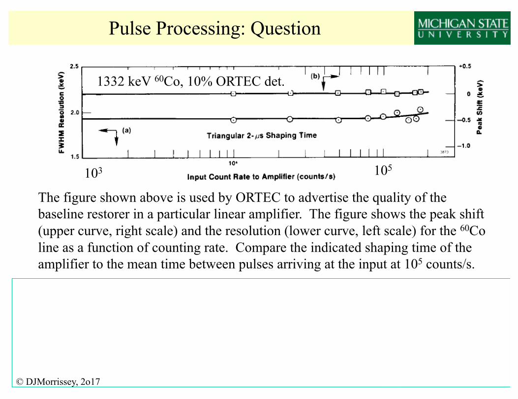
Pulse Processing: Question
103 105
1332 keV 60Co, 10% ORTEC det.
The figure shown above is used by ORTEC to advertise the quality of the baseline restorer in a particular linear amplifier. The figure shows the peak shift (upper curve, right scale) and the resolution (lower curve, left scale) for the 60Co line as a function of counting rate. Compare the indicated shaping time of the amplifier to the mean time between pulses arriving at the input at 105 counts/s.
5 10 15 20
0.05
0.1
0.15
0.2
0.25
0.3
0.35
€
Vout =Vintτ
#
$ % &
' ( e− t /τ for CR −RC shaping t = 1/r =10-5s
© DJMorrissey, 2o17