vuv-sensitive silicon photomultipliers for xenon ... · vuv-sensitive silicon photomultipliers for...
TRANSCRIPT

PREPARED FOR SUBMISSION TO IEEE TRANSACTIONS ON NUCLEAR SCIENCE 1
VUV-sensitive Silicon Photomultipliers for XenonScintillation Light Detection in nEXO
A. Jamil, T. Ziegler, P. Hufschmidt, G. Li, L. Lupin-Jimenez, T. Michel, I. Ostrovskiy, F. Retiere, J. Schneider,M. Wagenpfeil, A. Alamre, J. B. Albert, G. Anton, I. J. Arnquist, I. Badhrees, P. S. Barbeau, D. Beck, V. Belov,
T. Bhatta, F. Bourque, J. P. Brodsky, E. Brown, T. Brunner, A. Burenkov, G. F. Cao, L. Cao, W. R. Cen, C. Chambers,S. A. Charlebois, M. Chiu, B. Cleveland, M. Coon, M. Cote, A. Craycraft, W. Cree, J. Dalmasson, T. Daniels,L. Darroch, S. J. Daugherty, J. Daughhetee, S. Delaquis, A. Der Mesrobian-Kabakian, R. DeVoe, J. Dilling,
Y. Y. Ding, M. J. Dolinski, A. Dragone, J. Echevers, L. Fabris, D. Fairbank, W. Fairbank, J. Farine, S. Feyzbakhsh,R. Fontaine, D. Fudenberg, G. Gallina, G. Giacomini, R. Gornea, G. Gratta, E. V. Hansen, D. Harris, M. Hasan,
M. Heffner, J. Hoßl, E. W. Hoppe, A. House, M. Hughes, Y. Ito, A. Iverson, C. Jessiman, M. J. Jewell, X. S. Jiang,A. Karelin, L. J. Kaufman, T. Koffas, S. Kravitz, R. Krucken, A. Kuchenkov, K. S. Kumar, Y. Lan, A. Larson,D. S. Leonard, S. Li, Z. Li, C. Licciardi, Y. H. Lin, P. Lv, R. MacLellan, B. Mong, D. C. Moore, K. Murray,
R. J. Newby, Z. Ning, O. Njoya, F. Nolet, O. Nusair, K. Odgers, A. Odian, M. Oriunno, J. L. Orrell, G. S. Ortega,C. T. Overman, S. Parent, A. Piepke, A. Pocar, J.-F. Pratte, D. Qiu, V. Radeka, E. Raguzin, T. Rao, S. Rescia,
A. Robinson, T. Rossignol, P. C. Rowson, N. Roy, R. Saldanha, S. Sangiorgio, S. Schmidt, A. Schubert, D. Sinclair,K. Skarpaas VIII, A. K. Soma, G. St-Hilaire, V. Stekhanov, T. Stiegler, X. L. Sun, M. Tarka, J. Todd, T. Tolba,
T. I. Totev, R. Tsang, T. Tsang, F. Vachon, B. Veenstra, V. Veeraraghavan, G. Visser, J.-L. Vuilleumier, Q. Wang,J. Watkins, M. Weber, W. Wei, L. J. Wen, U. Wichoski, G. Wrede, S. X. Wu, W. H. Wu, Q. Xia, L. Yang, Y.-R. Yen,
O. Zeldovich, X. Zhang, J. Zhao, Y. Zhou
Abstract—Future tonne-scale liquefied noble gas detectors de-pend on efficient light detection in the VUV range. In thepast years Silicon Photomultipliers (SiPMs) have emerged as avalid alternative to standard photomultiplier tubes or large areaavalanche photodiodes. The next generation double beta decayexperiment, nEXO, with a 5 tonne liquid xenon time projec-tion chamber, will use SiPMs for detecting the 175nm xenonscintillation light, in order to achieve an energy resolution ofσ/Qββ = 1%. This paper presents recent measurements ofthe VUV-HD generation SiPMs from Fondazione Bruno Kesslerin two complementary setups. It includes measurements of thephoton detection efficiency with gaseous xenon scintillation lightin a vacuum setup and dark measurements in a dry nitrogengas setup. We report improved photon detection efficiency at175nm compared to previous generation devices, that wouldmeet the criteria of nEXO. Furthermore, we present the projectednEXO detector light collection and energy resolution that could beachieved by using these SiPMs.
Index Terms—silicon photomultiplier, xenon detectors, photodetectors, vacuum ultra-violet light, nEXO
I. NEUTRINO-LESS DOUBLE BETA DECAY AND NEXO
N eutrino-less double beta decay (0νββ) is a hypotheticalnuclear decay where two neutrons decay into two protons
and two electrons are emitted but no anti-neutrinos are presentin the final state. The observation of this process would have afundamental impact on the Standard Model of Particle Physics,specifically showing a violation of lepton number conservation(|∆L| = 2), and would imply that the neutrino is a Majoranafermion [1], independently of the actual process enabling thedecay [2]. Furthermore, the half-life of the decay would shedlight on the absolute neutrino mass scale [3].
Manuscript received June 8, 2018; revised August 29, 2018. Please seeAcknowledgment section for author affiliations.
The nEXO collaboration plans to build a cylindrical single-phase time projection chamber (TPC) filled with 5 tonnesof liquid xenon (LXe), with 90 % enrichment in 136Xe [4].nEXO takes advantage of the experience from its predecessorEXO-200 [5], but will incorporate new light and charge detec-tors [6]. Together with cold electronics sitting inside the LXe,this allows nEXO to achieve an energy resolution of σ/Qββ =1 % for the 0νββ decay of 136Xe (2458.07± 0.31 keV [7], [8]).In particular, instead of the EXO-200 Large Area AvalanchePhoto-diodes (LAAPDs), nEXO will use Silicon Photomulti-pliers (SiPMs) for the detection of xenon scintillation light. TheSiPMs will fully cover the lateral surface of the cylinder with atotal photo-sensitive area of about 4 m2, as shown in Figure 1.The devices will be immersed in LXe and placed in the highfield region behind the field shaping rings of the TPC fieldcage [9]. The performance of SiPMs has improved significantlyover the past decade and they are especially interesting becauseof their high gain, on the order of 106, and their single photonresolution capability.
The half-life sensitivity of nEXO to the 0νββ decay of 136Xeis projected to be 9.5× 1027 yr for 90 % C.L. after 10 years ofdata taking [4]. According to recent work [10], nEXO is oneof the planned double beta decay experiments with the bestdiscovery potential. In order to achieve the anticipated energyresolution and sensitivity, the nEXO collaboration has startedan extensive characterization campaign of SiPMs to find theoptimal candidate [11] and is working together with differentvendors, in particular Fondazione Bruno Kessler (FBK) [12]and Hamamatsu Photonics K.K. [13]. The most importantparameters to consider are:
arX
iv:1
806.
0222
0v3
[ph
ysic
s.in
s-de
t] 1
3 M
ar 2
019

2 PREPARED FOR SUBMISSION TO IEEE TRANSACTIONS ON NUCLEAR SCIENCE
118 c
m
124 c
m
Fig. 1. Conceptual arrangement of SiPMs inside the nEXO TPC. The SiPMswill be grouped into tiles of 8 × 8 dies with 30 tiles mounted onto staves, anda total of 24 staves to cover the whole lateral surface. The full assembly is124 cm in height and 118 cm in diameter and will incorporate about 4m2 ofSiPMs.
• The Photon-detection efficiency (PDE). This is defined as
PDEmeasured = PDE · (1− r(θ))= εgeo · Ptrig ·QE · (1− r(θ)) (1)
where Ptrig is the probability that a photoelectron triggersan avalanche, QE is the quantum efficiency and εgeo isthe ratio of photo-sensitive area to overall surface area.In general, the PDE also depends on the angle-dependentreflectance r(θ) of the SiPM surface. Important for theenergy resolution is the overall light collection efficiency
ε0 = PDE · PTE (2)
where PTE is the photon transport efficiency, which isdefined as the fraction of photons that are absorbed in theSiPMs relative to the number of originally emitted pho-tons. Both a high PDE and high reflectivity of componentswithin the TPC (high PTE) are crucial to minimize theloss of photons. More than half of the light impinging onthe SiPMs is expected to be reflected due to the mismatchin refractive indexes between the SiPM surface and LXe.A detailed understanding of reflectance as a function ofthe angle of incidence on the SiPM surface is necessary toincrease the quality of the simulations at reproducing ε0.According to current simulations, a PDE of at least 15 %and a PTE of 20 % is sufficient to achieve a σ/Qββ = 1 %energy resolution.
• Correlated avalanches. These are secondary avalanchesthat are not triggered directly by an initially absorbedphoton or a dark event. We can define two sub-categories(that themselves can be further sub-categorized): opticalcrosstalk and afterpulsing. The former process is dueto photon emission by electrons in collisions during theavalanche that could trigger another avalanche in another
microcell. The latter effect occurs when an electron inthe avalanche region is trapped in a lattice defect andtriggers an additional avalanche after being released. Thetwo processes can be distinguished by studying the timedistribution of events relative to the prompt pulse (trig-gered pulse) (see Figure 4 in section III-A). In order toreach nEXO design performance, the fraction of correlatedavalanches of both types combined per parent avalanchewithin a time window of 1 µs should be at most 20 %. Thehigher this value, the larger the contribution to the overallfluctuations of detected photons will be, resulting in worseenergy resolution.
• Gain and capacitance per unit area. The signal-to-noiseratio of the front-end electronics for single-photoelectronsdepends on both SiPM gain and capacitance per unitarea [14], [15]. This, under a power consumption con-straint, sets an upper limit on the total area one channel ofthe front-end electronics can read out. Since there is littleinformation on the geometrical origin of the scintillationlight, complexity is minimized by grouping several SiPMsinto a single readout channel and, at present, it is assumedthat 6 cm2 will be read out by one channel. This can beachieved as long as the specific capacitance of the SiPMsis below 50 pF mm−2 and the sum of gain fluctuations andelectronics noise is smaller than 0.1 p.e. In addition, priorto the assembly SiPMs with similar behavior in terms ofgain and breakdown voltage will be identified and groupedtogether.
This work focuses on the VUV-HD SiPMs from FBK withenhanced PDE at 175 nm. These SiPMs have a so-called low-field (LF) and standard-field (STD) version, which differ intheir doping profile. Both have a surface area of 5.56 ×5.96 mm2 and are made up of an array of 4 smaller SiPMs,which have been connected in parallel. These devices havea microcell pitch of 30 µm and total of ∼700 microcells per1 mm2. The breakdown voltage of the STD and LF deviceswere measured to be 22.8 V and 28.8 V at 169 K, respectively.We present results from complementary setups at Stanford andErlangen. The former one is used for efficiency measurementsthat help identifying potential SiPMs candidates. Measure-ments with the latter setup are aimed for better understandingof the devices properties in order to improve future SiPMstogether with vendors. These results are then used to infer theperformance of the nEXO detector in terms of the achievableenergy resolution.
II. HARDWARE AND SIGNAL PROCESSING
A. Stanford Setup
The Stanford group operates a test setup for characterizingSiPMs in vacuum with Xe scintillation light. It was optimizedfor efficiently determining the PDE of ∼1 cm2 size SiPMs.Figure 2 shows a cross-sectional view of the vacuum chamber(5), containing the cooling system, the source and the detectorcage. The light source is custom made and consists of a quartz-stainless steel capsule filled with a xenon atmosphere at about1 bar. Inside the capsule, 252Cf, electroplated onto a platinumsurface (7), produces xenon scintillation light after an α-decay

JAMIL et al.: VUV-SENSITIVE SILICON PHOTOMULTIPLIERS FOR XENON SCINTILLATION LIGHT DETECTION IN NEXO 3
4
1
8
2
7
9
5 6
310
8 m
m
Fig. 2. Cross-sectional view of the SiPM test setup at Stanford. The custommade scintillation light source (7) is at the bottom of the vacuum chamber(5). The detector cage (1) and the detectors (9) are cooled through a coppertube (6), that is brazed onto it and flushed with liquid nitrogen boil-off gas.The scintillation light that leaves the optical window (4) is confined withina PTFE sphere (8) to eliminate parasitic reflections off materials inside thevacuum chamber. In addition, a wavelength bandpass filter (2) is placed on topof the PTFE sphere. For a calibration of the detectors an optical fiber (3), thatis connected to an LED outside of the vacuum chamber, is mounted to outsideof the PTFE sphere (not shown in figure).
or spontaneous fission. The photons leave the source assemblythrough a quartz window (4). A cavity made out of PTFE(known to be a good reflector in the VUV range) is interposedbetween the Xe scintillation source and the photodetectors,improving the light collection, while at the same time avoidingpossible inconsistencies and systematics due to light scatteringby the many complex materials in the vacuum chamber. Thespherical shape of the reflector does not have a specific functionin the current version of the setup. In addition, an opticalbandpass filter (2) with a transmission curve centered at 180 nmand a width of 40 nm FWHM was placed at the top openingon the detector side of the PTFE sphere. The bandpass filtereliminates photons other than the 175 nm xenon scintillationlight – e.g. PTFE’s re-emission (conversion, fluorescence) atlonger wavelengths and the sub-dominant infra-red componentof the xenon scintillation spectrum. An optical fiber (3) allowsthe calibration of the reference PMT and the SiPMs (9) witha light source of varying intensity and wavelength. The fiberis mounted to the outside of the PTFE sphere (not shown infigure) and connected to an LED located outside the vacuumchamber. Throughout this work we have used a blue LED forthe calibration.
The detectors are placed inside a copper box (1) at the topof the vacuum chamber with a few mm distance to the opticalbandpass filter. Since the setup only allows measurement ofone detector at a time, different insets were made to allowpositioning the reference PMT and the different SiPMs at anequal distance to the light source. In order to avoid electronics
SECTION B-BSCALE 2 : 1
B
B
1
2
5
3
6
7
8
9
4
32 m
m
Fig. 3. Cross-section of the Erlangen SiPM test setup showing the inner vacuumcontainment (1). It comprises the copper cup (2) containing the xenon, thecooling finger (5), both PMT (3) and SiPM stack, combining SiPM board(6) and amplification board (7), the PTFE detector holder (8) and the tubeconnector to the electrical feedthroughs on top (9). The α-source (4) can beplaced inside an inset at the bottom of the copper cup.
pick-up, PTFE spacers were used to electrically isolate thecopper box from the rest of the vacuum chamber. Copper pipes(6) are brazed to the bottom perimeter of copper box, providingcooling by a flow of nitrogen boil-off gas. The temperatureis controlled by resistive heaters, attached to the ingoing pipeand controlled by Omega PID controllers [16], to allow stablemeasurements at the LXe temperature in nEXO at around169 K, with a variation of 0.5 K. The vacuum achieved by thissetup is better than 1× 10⁻⁶ mbar. The system is designedfor fast cooldown from room temperature and can reach stableoperations in ∼1.5 h.
B. Erlangen Setup
The Erlangen SiPM test setup consists of an inner xenoncell contained in an outer vacuum vessel (1). The xenon cellincorporates the detectors used for dark and xenon scintillationlight measurements. Figure 3 shows a cross-sectional viewwhere one can see the SiPM stack of two printed circuit boardson the right and a VUV-sensitive PMT (3), R8520-406 fromHamamatsu, on the left. The SiPM stack consists of the SiPMcarrier board (6) and a custom made preamp board (7). BothPMT and SiPM stacks are held in place by a PTFE structure(8) which hangs down from a copper bracket at the top of thexenon cell, thus having the detectors facing downwards. Thewhole xenon cell is enclosed by a copper cup (2) with a wallthickness of 1 cm for thermal conductivity reasons. Besides thedetector assembly, the xenon cell also contains a copper inletat the bottom in which an α-source (4) can be installed forthe emission of xenon scintillation light by α-particles movingthrough and ionizing the xenon within the cell.
The entire copper cup is enclosed within the inner steel vac-uum vessel. The vessel is connected to electrical feedthroughs

4 PREPARED FOR SUBMISSION TO IEEE TRANSACTIONS ON NUCLEAR SCIENCE
Device Uop [V] Ubreak [V] Setup Temperature [K]LF E 33-36.5 29.42 Erlangen 168LF S1 30-33 28.74 Stanford 169LF S2 30-34 28.83 Stanford 169STD S 23.5-26 22.82 Stanford 169PMT 1190 - Stanford 293
TABLE IOVERVIEW OF THE KEY PARAMETERS FOR THE MEASUREMENTS OF THE
VARIOUS DEVICES.
for signal, bias voltage and the Resistance Temperature Detec-tor (RTD) cables as well as connections to the xenon gas inletsystem at the top of the vacuum chamber (9). A turbomolecularpump, realizing a pressure better than 2× 10⁻⁵ mbar, is alsoconnected from the top.
All cables are PTFE coated to minimize outgassing withinthe xenon cell. Signals are sent to an oscilloscope via isolatedBNC feedthroughs. The temperature is monitored with four100 Ohm Pt RTDs attached to the outside of the copper cupat three different heights as well as directly at the SiPM boardto monitor the actual SiPM temperature.
The bottom of the inner vacuum vessel sits on top of a coppercold finger (5) which is thermally linked to a liquid nitrogendewar outside of the outer vacuum. The cooling power can befine-tuned via ceramic resistors around the cooling finger. Thisallows cooling down the entire xenon cell to temperatures at168 K and guarantees long-term stabilization within 0.1 K. Thecopper cup allows the fast compensation of any heat flow fromthe top feedthroughs and direct cooling of the detectors.
III. MEASUREMENTS
An overview of the measurements that were carried out canbe found in Table I. Overall, three LF version SiPMs of thesame wafer were measured, one with the Erlangen (LF E) andtwo with the Stanford setup (LF S1 and LF S2). In addition,one STD version SiPM (STD S1) and a Hamamatsu PMT weremeasured with the Stanford setup.
A. SiPM Dark Measurements
Parameters such as dark count rate, recovery time constant,crosstalk and after-pulsing probability were measured in thecryogenic setup in Erlangen at temperatures of 168 K. Thexenon chamber was used without a radioactive source andwas filled with gaseous nitrogen during these measurements.An FBK LF device (which will be referred to as LF E) wasmeasured between overvoltages of about 3 V to 7 V. Dataacquisition was triggered by signals exceeding the electronicsnoise. The waveforms were 10 µs long and were sampled witha rate of 2.5 GS/s.
To assess device characteristics, pulses in the waveformsare analyzed in a multi-stage algorithm, starting with the peakfinder TSpectrum provided by ROOT [17] and using the knownpulse shape. χ2-fits to these pulses are performed with a pulserepresentation comprising an exponentially modified Gaussiandistribution. After a first fit iteration, the pulse shape is set byfixing both rise time and fall time of the pulses to the ensemble’s
most probable values. Depending on the overvoltage the riseand fall times would vary between 2.3 ns to 2.8 ns and 78.7 nsto 86.1 ns, respectively. A second fit iteration is performedwith fixed pulse shape to improve the estimation of pulsetime and amplitude. For fits exceeding a certain threshold ofreduced χ2
red, test pulses are added iteratively to the fit. Thenew pulse combination is kept permanently if the value ofχ2
red of the new fit improves significantly. Otherwise, the testpulses are discarded. The last step of the algorithm improves thecapability to identify overlapping pulses. Using this algorithm,pulses more than about 10 ns apart can be separated reliably.The distribution of these amplitudes, converted into number ofphotoelectron equivalents (p.e.) as function of the time sincethe trigger is shown in Figure 4. This representation allowsthe identification of the various origins of the backgroundsignal, such as thermally induced avalanches. The microcells’recharging process and effects contributing to correlated noise,including prompt and delayed crosstalk and after-pulsing canbe identified as well. Prompt pulses (circled in blue) gatheraround 1 p.e. and dominantly lie within the first 10 ns. Promptpulses producing prompt crosstalk (circled in dashed blue) aremeasured as pulses with multiple p.e. as photons emergingfrom the avalanche are detected quasi-instantaneously in an-other microcell. Avalanches due to delayed crosstalk (circled inpurple), which contributes negligibly, originate from photonsbeing absorbed in passive components of another microcellwhere the photoelectron diffuses to the active part of that micro-cell. Due to timing, these delayed avalanches produce anotherdistinct trigger and are identified separately as additional pulseswith 1 p.e. [11]. Triggered pulses suffering afterpulsing (circledin orange), describing the release of trapped charge carriers ofan avalanche, are measured as a parent pulse and a correlateddelayed pulse. Since these delayed pulses can suffer crosstalkas well, the band structure is repeated above 1 p.e. (circledin dashed orange). Pulses occurring with larger delay to theparent pulse can originate from either afterpulsing or thermalexcitation (circled in green) and can suffer prompt crosstalk aswell (circled in dashed green). Pulses occurring shortly aftera prompt pulse in a previously triggered microcell, which aretypically afterpulses, have lower amplitudes since the microcellcharge has not been fully replenished yet. The assignment to af-terpulsing or dark events can only be done on a statistical basis.The pulses marked circled in dashed purple do not correspondto any physical effect but are due to misidentification by thepeak finder and are omitted in the further analyses.
The charge distribution of prompt pulses is used to determineprompt crosstalk. Due to this process, the average charge inprompt pulses exceeds the mean response of a single microcellQ1 p.e.. Thus, the mean number of prompt crosstalk avalanchesNCT is conventionally defined as:
NCT =1
N
N∑i=1
Qi −Q1p.e. , (3)
where the normalized sum is the average charge in promptpulses. This quantity can be larger than one and also includeshigher order crosstalk processes, i.e. avalanches produced bycrosstalk that themselves induce additional avalanches via

JAMIL et al.: VUV-SENSITIVE SILICON PHOTOMULTIPLIERS FOR XENON SCINTILLATION LIGHT DETECTION IN NEXO 5
0
1
2
3
100 101 102 103 104
promptcrosstalk
prompt
delayedcrosstalk
afterpulses anddark events
(afterpulses anddark events) suffering
prompt crosstalk
afterpulses su
ffering
prompt crosstalk
afterpulses
Charge
[p.e.]
Time after trigger [ns]
0
1
2
3
100 101 102 103 104100
101
102
Number
ofevents
Fig. 4. Distribution of photoelectron equivalents for parent and subsequent pulses as a function of the time since the microcell was triggered. See text for detailedexplanation. Data from Erlangen setup with LF E device at 5.58V overvoltage.
0.0
0.2
0.4
0.6
0.8
1.0
1.2
0 1 2 3 4 5 6 7 8
Meanad
ditional
charge
[p.e.]
Overvoltage [V]
LF ELF S1LF S2STD S
Fig. 5. The mean contribution of prompt crosstalk only (dashed line) and totalcorrelated noise (solid lines) as a function of overvoltage, which were measuredwith the Erlangen (blue) and Stanford (green, orange and purple) setup. Theyinclude correlated avalanche processes to all orders. Data from Stanford andErlangen setup.
crosstalk. The mean number of prompt crosstalk avalanchesNCT (blue dashed curve) is shown in Figure 5 for severalovervoltages. We emphasize that this quantity is different thanthe probability for prompt crosstalk to occur.
Afterpulsing is caused by the release of charge carrierstrapped within a previously triggered microcell. It can bedetermined by exploiting the distribution of time differencesbetween parent pulses resulting from a single avalanche andtheir subsequent pulse. The latter pulse can be of any amplitudeexceeding the noise level in order to not reject afterpulses beingaccompanied by prompt crosstalk. To obtain the dark count rateand the mean number of afterpulsing avalanches, the method
100
101
102
103
104
105
106
107
100 101 102 103 104 105 106 107 108 109
Pulserate
[Hz]
Time to next pulse [ns]
7.1 V4.6 V3.6 V
Fig. 6. Time distribution of the pulse rateR(t) for pulses occurring after a timedifference t with respect to the prompt parent pulse. Shown are distributionsobtained with an LF device in the Erlangen setup for several overvoltagesas denoted in the legend. The error bars are calculated assuming Poissonianuncertainties on the number of events corresponding to each bin. The details onthe selection of parent and subsequent pulses are explained in the text. Theflat part at long time differences corresponds to the dark count rate whosecontributions are indicated by the bands showing the mean value with standarddeviation, whereas shorter time differences are dominated by afterpulses. Datafrom Erlangen setup.
described in [18] is used which introduces a model-independentapproach to extract both quantities without the necessity offitting several time constants for de-trapping in lattice defects.
We emphasize that the mean number of afterpulses doesnot equal its correlated charge contribution since the releasedcharge of an avalanche depends on the microcell’s recoverystate. Detailed pulse selection on both primary and secondarypulses are applied as stated in [18]. Assuming Poissonian statis-

6 PREPARED FOR SUBMISSION TO IEEE TRANSACTIONS ON NUCLEAR SCIENCE
0.0
0.1
0.2
0.3
0.4
0.5
0.6
0.7
0.8
3 4 5 6 7 8
Meannumber
ofad
ditional
avalanches
Overvoltage [V]
Afterpulsing (1 µs)Afterpulsing (1ms)
Fig. 7. The mean number of additional avalanches due to afterpulsing as afunction of the overvoltage measured with an LF device in the Erlangen setup.Here, two different time-windows are considered to determine the impact ofafter-pulsing: the first 1 µs and the first 1ms after the primary avalanche. Datafrom Erlangen setup.
tics, the probability pi for a secondary pulse to occur betweentimes ti and ti+1 relative to the initial pulse is given by:
pi = e−βi · (1− e−λi) (4)
where βi and λi denote the average number of correlated pulsesbefore time ti and between time ti and ti+1, respectively. Thefirst part of the function accounts for no pulses up to timeti, whereas the second part accounts for at least one pulseoccurring between time ti and ti+1. Exploiting the sequentialnature of βi =
∑i−1j=0 λj , one can calculate λi iteratively for
any time window by inverting Equation 4 and using β0 = 0.The correlated pulse rate can then be simply calculated as
Ri =λi
ti+1 − ti. (5)
Example distributions of the pulse rate are shown in Figure 6.The excess in rate due to afterpulses vanishes for long timedifferences, leaving only the contribution due to dark events.Summing the excess at time differences below 1 µs yieldsthe mean number of afterpulses that is of particular interestfor nEXO and is shown in Figure 7 for several overvoltages.Assuming no contributions from afterpulsing after 1 ms, wecan consider this number to be the overall mean number ofafterpulses. The dark count rate can be extracted by fittingthe part of the distribution above 1 ms with a flat function.Even though the distributions in our measurements are notperfectly flat after 1 ms, we use them to determine the darkcount rate. For this reason, we state the distribution of valuesat a given overvoltage rather than the mean value as shownin Figure 8. The dark count rate does not exceed 2 Hz mm−2,well below the limit of 50 Hz mm−2 required by nEXO. Thecontribution due to delayed crosstalk is not modeled separatelyhere but is incorporated in the mean number of afterpulses. Itscontribution compared to afterpulsing is negligible as can beseen in Figure 4.
0
0.5
1
1.5
2
2.5
3 4 5 6 7 8
Darkcountrate
[Hzmm
−2]
Overvoltage [V]
Fig. 8. Box plot of dark count rate per unit area of the LF E device forseveral overvoltages. The surface area on the front face of the device is5.56× 5.96mm2. Data points with delays exceeding 1ms in the distributionsin Figure 8 contribute to this plot. The box indicates the area between the 1st and3rd quartile (25%-75% of the data points) whereas the 2nd quartile (medianvalue) is shown as horizontal bar inside the box. The whiskers comprise 95%of the data points around the median. Data points outside that range are shownindividually as outliers. Data from Erlangen setup.
101
102
103
104
0 0.01 0.02 0.03 0.04 0.05 0.06
Number
ofevents
Charge [a.u.]
DataOverall FitGauss. Contr.Noise Contr.
Fig. 9. Typical response of the reference PMT at Stanford to an LED operatedat low light level. By fitting the function described in Formula 7, the value forthe 1p.e. charge response Q1 can be extracted and used to calibrate the PMT.The overall fit is shown as solid blue line, whereas the different p.e. orders ofthe fit are dashed green and the background contribution is shown as a dashedorange curve. Data from Stanford setup.
B. Reference PMT Calibration
In order to measure the absolute PDE of the SiPMs reliably,a calibrated R9875P PMT from Hamamatsu [19] was used as areference detector in the Stanford setup. The PMT has a 11 mmwide synthetic silica entrance window and Cs-Te photocathodewith roughly 8 mm in diameter. It was operated at 1190 V forwhich a quantum efficiency (QE) at 175 nm of 14 % and acollection efficiency (CE) of the first dynode of 70.6 % wasmeasured by Hamamatsu.
The single photon response can be extracted from a measure-
JAMIL et al.: VUV-SENSITIVE SILICON PHOTOMULTIPLIERS FOR XENON SCINTILLATION LIGHT DETECTION IN NEXO 7
ment with a pulsed LED. The PMT is placed inside the detectorcage and the xenon scintillation light was blocked by placing athick black sheet on top of the bandpass filter. The light level ofthe LED inside the vacuum chamber is set very low, such thatthe PMT roughly only sees about one photon every ten LEDpulses. An ideal photomultiplier response follows a Poissondistribution. However, there are various background processesthat will contribute to the signal, e.g. thermoelectric emissionfrom the photo-cathode or the dynodes, and ultimately leadto an additional charge noise contribution. The contributionof these processes to the charge spectrum can be expectedto decrease exponentially with charge. Thus, the real PMTresponse will be composed of a Poisson-convoluted Gaussiandistribution of the true signal and the distribution of the noisecontribution. It can be expressed as [20]
f(q) =
[1− ωσ0√
2π· exp
(− (q −Q0)2
2σ20
)(6)
+ ω · θ(q −Q0) · α exp (−α(q −Q0))]· e−µ
+
k∑n=1
µne−µ
n!
1
σ1√
2πnexp
(− (q −Q0 −Qsh − nQ1)2
2nσ21
)where q is the measured charge, ω is the probability for abackground process to happen, α the coefficient of exponentialdecrease of discrete background processes and µ the mean num-ber of the detected photoelectrons. Q0, σ0, Q1 and σ1 are themean value and the standard deviation of the pedestal and thesingle photon response, respectively. Furthermore, Qsh = ω/αintroduces a shift of the true p.e. pulses due to the backgroundcontribution. An example fit to the PMT response is shown inFigure 9.
C. Absolute PDE Measurement
The absolute PDE of two LF (LF S1 and LF S2) and one STD(STD S) version SiPMs was measured with the Stanford setup.The PDE determination is based on a comparison of the amountof light that was seen by both the calibration PMT and theSiPM. Given the known QE and CE of the PMT and a propercalibration of the single photon response, one can determinethe amount of light detected by the reference detector. Togetherwith the measured response of the SiPMs one can translate thisinto an absolute PDE for the SiPM.
At Stanford the SiPM signals are transported with flex-ible solid-core cables and through a grounded-shield BNCfeedthrough. A CAEN digitizer (DT5724 [21]) records 10 µslong waveforms with a sampling rate of 100 Ms/s after thesignal has been amplified in a Cremat charge-sensitive amplifier(CR-110 [22]) and a Gaussian shaper (CR-200 [23]) with a100 ns shaping time. The data is analyzed with a custom C++-based software that uses ROOT [17]. The waveforms wereintegrated over a fixed time window of 1 µs after the trigger toobtain the collected charge of the event. To allow a comparisonof the mean light fluence seen by both detectors, the integratedcharge was normalized by the respective gain and the surfacearea of the devices.
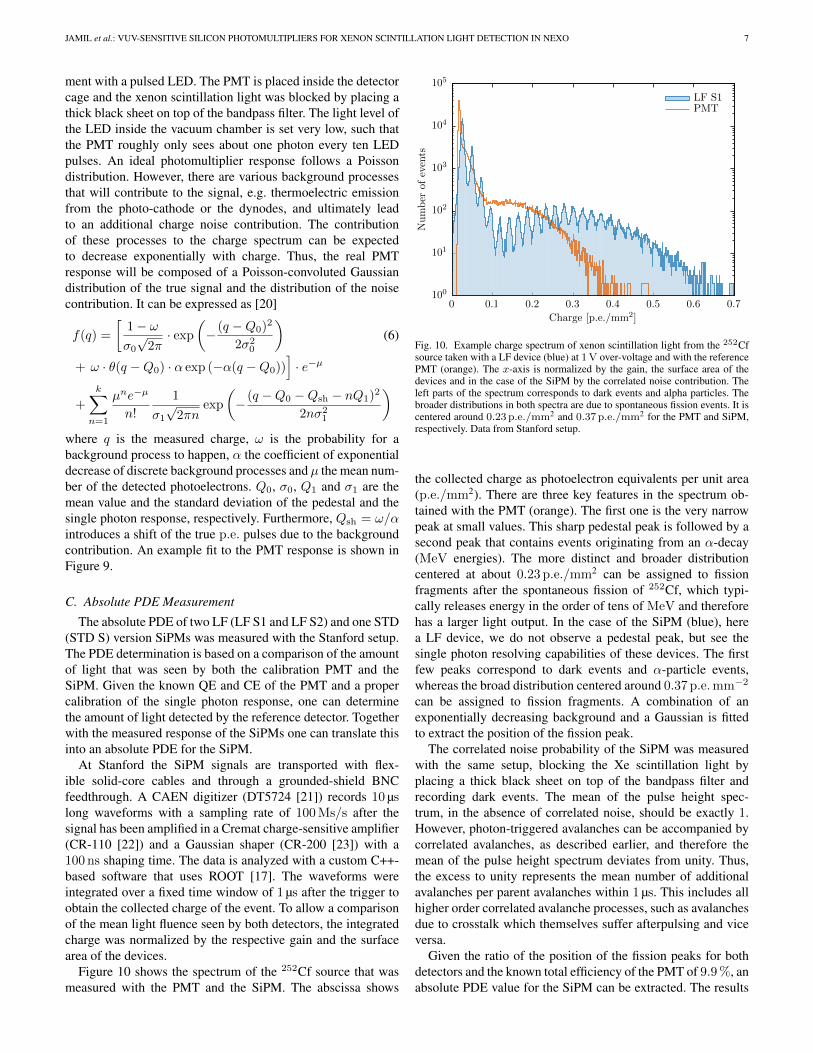
Figure 10 shows the spectrum of the 252Cf source that wasmeasured with the PMT and the SiPM. The abscissa shows
100
101
102
103
104
105
0 0.1 0.2 0.3 0.4 0.5 0.6 0.7
Number
ofevents
Charge [p.e./mm2]
LF S1PMT
Fig. 10. Example charge spectrum of xenon scintillation light from the 252Cfsource taken with a LF device (blue) at 1V over-voltage and with the referencePMT (orange). The x-axis is normalized by the gain, the surface area of thedevices and in the case of the SiPM by the correlated noise contribution. Theleft parts of the spectrum corresponds to dark events and alpha particles. Thebroader distributions in both spectra are due to spontaneous fission events. It iscentered around 0.23p.e./mm2 and 0.37p.e./mm2 for the PMT and SiPM,respectively. Data from Stanford setup.
the collected charge as photoelectron equivalents per unit area(p.e./mm2). There are three key features in the spectrum ob-tained with the PMT (orange). The first one is the very narrowpeak at small values. This sharp pedestal peak is followed by asecond peak that contains events originating from an α-decay(MeV energies). The more distinct and broader distributioncentered at about 0.23 p.e./mm2 can be assigned to fissionfragments after the spontaneous fission of 252Cf, which typi-cally releases energy in the order of tens of MeV and thereforehas a larger light output. In the case of the SiPM (blue), herea LF device, we do not observe a pedestal peak, but see thesingle photon resolving capabilities of these devices. The firstfew peaks correspond to dark events and α-particle events,whereas the broad distribution centered around 0.37 p.e.mm−2
can be assigned to fission fragments. A combination of anexponentially decreasing background and a Gaussian is fittedto extract the position of the fission peak.
The correlated noise probability of the SiPM was measuredwith the same setup, blocking the Xe scintillation light byplacing a thick black sheet on top of the bandpass filter andrecording dark events. The mean of the pulse height spec-trum, in the absence of correlated noise, should be exactly 1.However, photon-triggered avalanches can be accompanied bycorrelated avalanches, as described earlier, and therefore themean of the pulse height spectrum deviates from unity. Thus,the excess to unity represents the mean number of additionalavalanches per parent avalanches within 1 µs. This includes allhigher order correlated avalanche processes, such as avalanchesdue to crosstalk which themselves suffer afterpulsing and viceversa.
Given the ratio of the position of the fission peaks for bothdetectors and the known total efficiency of the PMT of 9.9 %, anabsolute PDE value for the SiPM can be extracted. The results

8 PREPARED FOR SUBMISSION TO IEEE TRANSACTIONS ON NUCLEAR SCIENCE
Source of Systematic Error Value [%]Solid angle 3Angular Distribution 1PMT gain stability 6PMT gain modeling 10PMT QE uncertainty ∼ 2PMT CE uncertainty ∼ 14Quadratic sum ∼ 19
Source of Statistical Error Value [%]PMT gain calibration 1SiPM gain calibration 1Correlated noise correction 1Fission peak position 1Quadratic sum 2
TABLE IISUMMARY OF SYSTEMATIC AND STATISTICAL ERROR SOURCES. THE
LATTER ONE IS THE STANDARD DEVIATION OF THE CORRESPONDING FITPARAMETER. THE LARGEST COMPONENT OF THE UNCERTAINTY IN
MEASURING THE PDE IS THE UNCERTAINTY ON THE CE OF THE PMT.SINCE THE ERROR SOURCES ARE INDEPENDENT, THE COMPONENTS ARE
ADDED IN QUADRATURE.
for three different (two LF and one STD type) devices areshown in Figure 11. The plot on the left-hand side shows the de-pendence of the PDE with over-voltage, where a slight increaseis observable. However, the efficiency saturates at relatively lowbias voltages, corresponding to a saturation of the probabilityto trigger an avalanche. The plot on the right-hand side showsthe PDE as a function of the number of additional avalancheswithin 1 µs. It shows that the LF devices meet our requirementsof more than 15 % PDE while keeping the correlated noiseprobability below 20 %. Generally, the LF devices seem to havea better operating range and performance since for a givencorrelated noise probability they can be operated at a higherovervoltage and therefore have a higher PDE. Also, from anelectronics point of view a higher overvoltage is desirable sincethis automatically means higher gain and better signal-to-noiseratio.
D. Systematic and Statistical Errors
The colored error bands and error bars in Figure 11 stemfrom several sources of systematic and statistical uncertainties,respectively. The individual components and their estimatedvalues are summarized in Table II. The PMT introduces themajor components for the systematics. The reference PMT hasbeen calibrated by Hamamatsu in order to get the respectivewavelength-dependent QE and the CE of this particular tube.The calibration was done at room temperature and at normalincidence. The QE was measured to be 14 % with a relativeuncertainty of about 2 %. For the collection efficiency (CE) atthe first dynode of the PMT a value of 70.6 % was determinedby Hamamatsu without any estimate for the uncertainty. Con-servatively, we assume (70 ± 10)% for the CE of the PMT.Furthermore, a variation of the PMT gain over time on the orderof 6 % was observed, which is due to temperature related gainvariations over time, caused by not cooling the PMT duringthe measurements. The statistical uncertainty on the PMT gainitself is relatively small and well below 1 %. In order to cover
possible variations due to the model dependence of our gaincalibration we assign another 10 % as an systematic error for thegain calibration. The bottom inset of the copper box is designedsuch that all detectors are at the same distance relative to thelight source. In order to take 1 − 2 mm offset variations withrespect to the light source at a distance of roughly 108 mmand different detector geometries into account, a 3 % systematicerror is considered for the solid angle. The value was extractedfrom an optical simulation of the setup with different detectors,using the Chroma software [24]. Furthermore, the simulationpredicts that a large fraction of photons are detected withouthaving been reflected and at angles close to normal incidence,i.e. (3± 1)◦. From our simulation we can infer that the effectof non-normal incidence on the PDE from photons that arereflected off the PTFE sphere is about ∼1 %. The SiPM gaincalibration can be performed reliably and with a sub-percentlevel accuracy, which is why we assign 1 % statistical error.Similarly for the position of the fission peak, which is extractedby fitting a combination of an exponential and a Gaussianfunction. We assign a value of 1 % for this uncertainty as well.Finally, the uncertainty on the correlated noise was determinedas the standard error on the mean of the pulse distribution that isobtained during a dark measurement and was found to be 1 %.
IV. EXPECTED PERFORMANCE FOR NEXO
The energy resolution in nEXO can be evaluated using asimple model that is useful to understand the trade-off betweenPDE and correlated noise that both increase with over-voltage.Two quantities are commonly measured in a LXe TPC in orderto optimize the energy resolution [25]: the scintillation light andthe number of released electrons which did not recombine. Inthe nEXO TPC, the electrons that are released during ionizationof the Xe atoms and did not recombine drift towards the anodes.We assume that due to the anti-correlation, each ionizationelectron that recombines produces a photon. The fraction ofrecombining electrons will be denoted as R. Hence, event byevent fluctuations of the number of electrons Q and photonsS produced are canceled out by performing the optimal linearcombination of the two channels.
The production of ionization electrons Q and scintillationphotons S can be parameterized as
Q =E
W· (1−R) (7)
S =E
W· (Si +R) (8)
with E the deposited energy (2458.07± 0.31 keV during the0νββ decay of 136Xe [7], [8]), W the effective energy requiredto create an electron-ion pair (W = 15.6 eV [26], [27]) andSi the fraction of scintillation photons produced by excitationrelative to ionization. Si is set to the most probable value of 0.13according to [28]. The optimum energy estimator O cancelingthe fluctuation of R is
O = S +Q =E
W· (Si + 1) . (9)
under the assumption that the electronics noise is smaller thanthe recombination noise.

JAMIL et al.: VUV-SENSITIVE SILICON PHOTOMULTIPLIERS FOR XENON SCINTILLATION LIGHT DETECTION IN NEXO 9
0
5
10
15
20
25
30
0 1 2 3 4 5 6
Photo
ndet
ecti
on
effici
ency
[%]
Overvoltage [V]
LF S1LF S2STD S
0
5
10
15
20
25
30
0 0.2 0.4 0.6 0.8 1 1.2
Photo
ndet
ecti
on
effici
ency
[%]
Additional avalanches within 1 µs
LF S1LF S2STD S
Fig. 11. Photon detection efficiency as a function of overvoltage (left) and the number of additional correlated avalanches within 1 µs (right). The error barsrepresent the statistical errors whereas the colored bands show the systematic errors, that are stated in Table II. These measurements show that within theuncertainties the required 15% PDE, while still having a correlated avalanche probability lower than 20%, are fulfilled for nEXO. However, a very small rangeof operation, only up to a few volts overvoltage, is possible. Data from Stanford setup.
In nEXO, the energy resolution is dominated by the noisein the light channel. Therefore, good energy resolution isstrongly coupled to the overall light collection efficiency. Thescintillation light will be detected by SiPMs covering up to4 m2. Moreover, the transport and photon detection efficiencyare entangled because the SiPM surface is very reflective at175 nm due to the large differences of the indices of refractionbetween silicon (nSi = 0.682), silicon dioxide (nSiO2
= 1.61)and LXe (nLXe = 1.66). The VUV-HD generation SiPMshave a 1.5 µm thick SiO2 layer on the top surface as an anti-reflective coating. Assuming a PDE of 15 %, our simulationsshow that an εo, i.e. the product of the PTE and the SiPMPDE, of ≥ 3 % is sufficient to achieve an energy resolution ofσ/Qββ ≤ 1 %. This corresponds to a PTE of 20 %, which canalready be achieved by a 60 % reflectivity of the cathode andthe field shaping rings and a 50 % reflectivity of the anode. Wewould like to emphasize that these assumptions are relativelyconservative. Therefore, the average number of photo-electronsis then 1985 at 2458 keV. The average number of dark eventswithin the longest possible integration window of 1 µs and forthe maximum measured value of 2 Hz mm−2 is only 10 and istherefore negligible.
As for the noise in the charge channel, ionization electronsare detected on pads without any amplification besides the elec-tronics preamplifier stage that introduces an equivalent noisecharge of about σq = 200 e− per channel. Given the currentchoice of 3 mm pixel pitch (studies of the optimal value are stillongoing), the charge of a 0νββ decay will be distributed overabout 10 channels on average, which will bring the equivalentnoise charge back to about σq = 600 e−. This is comparableto the value that was achieved by EXO-200 for one channel(σq = 800 e−) with a readout pitch of 9 mm. We can considerthis to be roughly the cut-off value below which the chargenoise can be considered sub-dominant for the overall energyresolution, as indicated by simulations where the effects of dif-fusion, electronics noise, and the channel multiplicity are taken
into account. This holds true as long as the main contributionto the energy resolution is noise from the light channel. As weimprove ε0 the improvement of the energy resolution will thenbe limited by σq . Other sources of fluctuations are known to benegligible.
With these assumptions, the average number of detectedSiPM avalanches A can be written as
A = εo · S · (1 + Λ) (10)
with εo the overall efficiency of detecting a scintillation photon,S the average number of scintillation photons, and Λ theaverage total number of correlated avalanches per avalanchewithin 1 µs at all orders. The optimum estimator can then bewritten as
O = Q+A
εo(1 + Λ). (11)
Introducing the Fano factor FQS for the combined productionof scintillation and ionization, the energy resolution (fluctua-tions of the optimum estimator) can be quantified as
σ2O = FQS ·O + σ2
Q +S
ε0
[(1− ε0) +
Λ
(1 + Λ)2
](12)
in the limit of small ε0. The value of FQS is not well known,and it is set to 1 conservatively although it could be as lowas 0.1 [26]. However, its contribution compared to the otherfactors is completely negligible. This equation also assumesthat the light detection is dominated by binomial fluctuationsdue to the finite efficiency of the SiPMs. Fluctuations of theproduction of correlated avalanches are modeled using Poissonstatistics for simplicity. Gain fluctuations and electronics noisefor the light channels can be safely neglected.
By using the values of ε0 and Λ obtained in the previoussections, this simple model allows the derivation of a functionaldependence of the energy resolution on the overvoltage of theSiPMs, as shown in Figure 12. The most dominant feature ofthis function is the existence of a minimum. Furthermore, the

10 PREPARED FOR SUBMISSION TO IEEE TRANSACTIONS ON NUCLEAR SCIENCE
0.7
0.8
0.9
1
1.1
1.2
1.3
1.4
0 1 2 3 4 5 6
Energyresolution[%
]
Overvoltage [V]
LF S1LF S2STD S
Fig. 12. Estimated energy resolution (as defined in Equation 12) for nEXO asa function of the overvoltage at which the SiPMs are operated. Using a simplemodel, that is described in more detail in the text, the optimal operation voltagefor the SiPM can be determined in order to minimize the energy resolution fornEXO. Due to the trade-off between increasing PDE and correlated noise, theminimal energy resolution is in general not achieved by choosing the largestovervoltage. The colored bands are propagated based on the systematic errorson the PDE. The curves are solely added as visual aid. Data from Stanfordsetup.
minimum does not coincide with the largest operation over-voltage, which in general results in a worse energy resolutionbecause of the increase of correlated noise, mostly due toafterpulsing.
V. CONCLUSION
A study of recent VUV-sensitive FBK SiPM types waspresented with a promising SiPM candidate that would meetnEXO’s requirements on the photon detection efficiency and theprobability for correlated avalanches within the uncertainties.Most specifically, the LF devices exceed the necessary 15 %PDE while maintaining a correlated noise probability of lessthan 20 %. More specifically, at about 2.2 V overvoltage theLF S1 and LF S2 devices have a PDE of about 20 % and17 % and a CN of 13 % and 15 %, respectively. While thesemeasurements were carried out in vacuum and simulationssuggest a straightforward translations of these results into LXe,it remains to be confirmed by measurements in LXe. Usinga simple model, we estimate the energy resolution of nEXO,taking into account the competing effects of increasing PDEand correlated noise with overvoltage. We predict to be able toreach and possible surpass the anticipated σ/Qββ = 1 %.
Looking forward, work is in progress to build a large scalelight detector module using the LF SiPMs, to be tested inLXe. Furthermore, work on readout electronics for a large scaleSiPM module is currently in progress with the goal to havea light detection module solution for nEXO. In addition, aparallel effort will study the angular dependence of the PDEin LXe, which was estimated to be negligible in the setup usedfor this study compared to the total systematic error budget.
ACKNOWLEDGMENT
This work has been supported by the Offices of Nuclearand High Energy Physics within DOEs Office of Science, andNSF in the United States, by NSERC, CFI, FRQNT, NRC,and the McDonald Institute (CFREF) in Canada, by BaCaTeCin Germany, by SNF in Switzerland, by IBS in Korea, byRFBR in Russia, and by CAS and ISTCP in China. Thiswork was supported in part by Laboratory Directed Researchand Development (LDRD) programs at Brookhaven NationalLaboratory (BNL), Lawrence Livermore National Laboratory(LLNL), Oak Ridge National Laboratory (ORNL) and PacificNorthwest National Laboratory (PNNL).
J. Dalmasson, R. DeVoe, D. Fudenberg, G. Gratta, A. Jamil, M. J. Jewell,G. Li, L. Lupin-Jimenez, S. Kravitz, A. Schubert, M. Weber and S. X. Wu arewith Physics Department, Stanford University, Stanford, CA 94305, USA (e-mail: [email protected]).
G. Anton, J. Hoßl, P. Hufschmidt, A. Jamil, T. Michel, S. Schmidt,J. Schneider, M. Wagenpfeil, G. Wrede and T. Ziegler are with Erlangen Centrefor Astroparticle Physics (ECAP), Friedrich-Alexander University Erlangen-Nurnberg, Erlangen 91058, Germany.
A. Jamil, Z. Li, D. C. Moore and Q. Xia are with Department of Physics,Yale University, New Haven, CT 06511, USA.
M. Hughes, O. Nusair, I. Ostrovskiy, A. Piepke, A.K. Soma and V. Veer-araghavan are with Department of Physics and Astronomy, University ofAlabama, Tuscaloosa, AL 35487, USA.
T. Brunner, J. Dilling, G. Gallina, R. Gornea, R. Krucken, F. Retiere andY. Lan are with TRIUMF, Vancouver, British Columbia V6T 2A3, Canada.
J. B. Albert, S. J. Daugherty, L. J. Kaufman and G. Visser are withDepartment of Physics and CEEM, Indiana University, Bloomington, IN 47405,USA.
I. J. Arnquist, E. W. Hoppe, J. L. Orrell, C. T. Overman, G. S. Ortega,R. Saldanha and R. Tsang are with Pacific Northwest National Laboratory,Richland, WA 99352, USA.
A. Alamre, I. Badhrees, W. Cree, R. Gornea, C. Jessiman, T. Koffas, D. Sin-clair, B. Veenstra and J. Watkins are with Department of Physics, CarletonUniversity, Ottawa, Ontario K1S 5B6, Canada.
P. Barbeau is with Department of Physics, Duke University and TriangleUniversities Nuclear Laboratory (TUNL), Durham, NC 27708, USA.
D. Beck, M. Coon, J. Echevers, S. Li and L. Yang are with PhysicsDepartment, University of Illinois, Urbana-Champaign, IL 61801, USA.
V. Belov, A. Burenkov, A. Karelin, A. Kuchenkov, V. Stekhanov andO. Zeldovich are with Institute for Theoretical and Experimental Physics namedby A. I. Alikhanov of National Research Center Kurchatov Institute, Moscow117218, Russia.
J. P. Brodsky, M. Heffner, A. House, S. Sangiorgio and T. Stiegler are withLawrence Livermore National Laboratory, Livermore, CA 94550, USA.
E. Brown and K. Odgers are with Department of Physics, Applied Physicsand Astronomy, Rensselaer Polytechnic Institute, Troy, NY 12180, USA.
T. Brunner, L. Darroch, Y. Ito, K. Murray and T. I. Totev are with PhysicsDepartment, McGill University, Montreal, Quebec H3A 2T8, Canada.
G. F. Cao, W. R. Cen, Y. Y. Ding, X. S. Jiang, P. Lv, Z. Ning, X. L. Sun,T. Tolba, W. Wei, L. J. Wen, W. H. Wu, X. Zhang and J. Zhao are with Instituteof High Energy Physics, Chinese Academy of Sciences, Beijing 100049, China.
L. Cao, D. Qiu, Q. Wang and Y. Zhou are with Institute of Microelectronics,Chinese Academy of Sciences, Beijing 100029, China.
C. Chambers, A. Craycraft, D. Fairbank, W. Fairbank, D. Harris, A. Iversonand J. Todd are with Physics Department, Colorado State University, Fort

JAMIL et al.: VUV-SENSITIVE SILICON PHOTOMULTIPLIERS FOR XENON SCINTILLATION LIGHT DETECTION IN NEXO 11
Collins, CO 80523, USA.F. Bourque, S. A. Charlebois, M. Cote, R. Fontaine, F. Nolet, S. Parent, J.-
F. Pratte, T. Rossignol, N. Roy, G. St-Hilaire and F. Vachon are with Universitede Sherbrooke, Sherbrooke, Quebec J1K 2R1, Canada.
M. Chiu, G. Giacomini, V. Radeka, E. Raguzin, T. Rao, S. Rescia andT. Tsang are with Brookhaven National Laboratory, Upton, NY 11973, USA.
B. Cleveland, A. Der Mesrobian-Kabakian, J. Farine, C. Licciardi, A. Robin-son and U. Wichoski are with Department of Physics, Laurentian University,Sudbury, Ontario P3E 2C6, Canada.
T. Daniels is with Department of Physics and Physical Oceanography,University of North Carolina at Wilmington, Wilmington, NC 28403, USA.
T. Bhatta, J. Daughhetee, M. Hasan, A. Larson and R. MacLellan are withDepartment of Physics, University of South Dakota, Vermillion, SD 57069,USA.
S. Delaquis, A. Dragone, L. J. Kaufman, B. Mong, A. Odian, M. Oriunno,P. C. Rowson and K. Skarpaas VIII are with SLAC National AcceleratorLaboratory, Menlo Park, CA 94025, USA.
M. J. Dolinski, E. V. Hansen, Y. H. Lin and Y.-R. Yen are with Departmentof Physics, Drexel University, Philadelphia, PA 19104, USA.
L. Fabris and R. J. Newby are with Oak Ridge National Laboratory, OakRidge, TN 37831, USA.
S. Feyzbakhsh and A. Pocar are with Amherst Center for FundamentalInteractions and Physics Department, University of Massachusetts, Amherst,MA 01003, USA.
K. S. Kumar, O. Njoya and M. Tarka are with Department of Physics andAstronomy, Stony Brook University, SUNY, Stony Brook, NY 11794, USA.
D. S. Leonard is with IBS Center for Underground Physics, Daejeon 34126,Korea.
J.-L. Vuilleumier is with LHEP, Albert Einstein Center, University of Bern,Bern CH-3012, Switzerland.
I. Badhrees’s Home Institutue is King Abdulaziz City for Science andTechnology, KACST, Riyadh 11442, Saudi Arabia.
G. F. Cao is also with University of Chinese Academy of Sciences, Beijing100049, China.
B. Cleveland is also with SNOLAB, Ontario, Canada.W. Cree is now at Canadian Department of National Defense.S. Delaquis is deceased.Y. Ito is now at JAEA, Ibaraki, Japan.S. Kravitz is now with Lawrence Berkeley National Lab, Berkeley, CA,
USA.A. Schubert is now with OneBridge Solutions, Boise, ID, USA.M. Tarka is now with University of Massachusetts, Amherst, MA, USA.X. Zhang is now with Tsinghua University, Beijing, China.
REFERENCES
[1] E. Majorana, “Teoria simmetrica dell’elettrone e del positrone,” Il NuovoCimento (1924-1942), vol. 14, no. 4, p. 171, Sep 2008.
[2] J. Schechter and J. W. F. Valle, “Neutrinoless double-β decay inSU(2)×U(1) theories,” Phys. Rev. D, vol. 25, pp. 2951–2954, Jun 1982.
[3] J. J. Gomez-Cadenas, J. Martin-Albo, M. Mezzetto, F. Monrabal, andM. Sorel, “The Search for neutrinoless double beta decay,” Riv. NuovoCim., vol. 35, pp. 29–98, 2012.
[4] nEXO collaboration, J. B. Albert et al., “Sensitivity and DiscoveryPotential of nEXO to Neutrinoless Double Beta Decay ,” 2017.
[5] EXO-200 collaboration, M. Auger et al., “The EXO-200 detector, part I:detector design and construction,” JINST, vol. 7, no. 05, p. P05010, 2012.
[6] nEXO collaboration, M. Jewell et al., “Characterization of an IonizationReadout Tile for nEXO,” JINST, vol. 13, no. 01, p. P01006, 2018.
[7] M. Redshaw, E. Wingfield, J. McDaniel, and E. G. Myers, “Mass anddouble-beta-decay Q value of 136Xe,” Phys. Rev. Lett., vol. 98, p.053003, Feb 2007.
[8] P. M. McCowan and R. C. Barber, “Q value for the double-β decay of136Xe,” Phys. Rev. C, vol. 82, p. 024603, Aug 2010.
[9] nEXO Collaboration, X. L. Sun et al., “Study of silicon photomultiplierperformance in external electric fields,” Journal of Instrumentation,vol. 13, no. 09, p. T09006, 2018. [Online]. Available: http://stacks.iop.org/1748-0221/13/i=09/a=T09006
[10] M. Agostini, G. Benato, and J. A. Detwiler, “Discovery probability ofnext-generation neutrinoless double-β decay experiments,” Phys. Rev. D,vol. 96, p. 053001, Sep 2017.
[11] I. Ostrovskiy et al., “Characterization of silicon photomultipliers fornEXO,” IEEE Trans. Nuclear. Sci., vol. 62, no. 4, pp. 1825–1836, Aug2015.
[12] Fondazione Bruno Kessler. [Online]. Available: https://www.fbk.eu/en/[13] Hamamatsu Photonics K.K. [Online]. Available: http://www.hamamatsu.
com/us/en/index.html[14] L. Fabris et al., “Concepts of SiPM readout electronics,” IEEE NSS/MIC,
2014. [Online]. Available: http://info.ornl.gov/sites/publications/Files/Pub52995.pptx
[15] L. Fabris, “Novel readout design criteria for SiPM-based radiationdetectors,” Ph.D. dissertation, University of Bergamo, 2015. [Online].Available: https://aisberg.unibg.it/retrieve/handle/10446/52227/107791/Binder Fabris DT.pdf
[16] Omega. [Online]. Available: https://www.omega.com/prodinfo/temperaturecontrollers.html
[17] R. Brun and F. Rademakers, “ROOT: An object oriented data analysisframework,” Nuclear Instruments. Methods, vol. A389, pp. 81–86, 1997.
[18] A. Butcher, L. Doria, J. R. Monroe, F. Retire, B. J. Smith, and J. J.Walding, “A method for characterizing after-pulsing and dark noise ofPMTs and SiPMs,” Nuclear Instruments. Methods A, vol. 875, pp. 87 –91, 2017.
[19] R9875SEL PMT from Hamamatsu. [Online]. Available: https://www.hamamatsu.com/resources/pdf/etd/R9875U TPMH1316E.pdf
[20] E. Bellamy et al., “Absolute calibration and monitoring of a spectrometricchannel using a photomultiplier,” Nuclear Instruments. Methods A, vol.339, no. 3, pp. 468 – 476, 1994.
[21] DT5725 Digitizer from CAEN. [Online]. Available: http://www.caen.it/csite/CaenProd.jsp?parent=14&idmod=625#
[22] Amplifier from Cremat. [Online]. Available: http://www.cremat.com/CR-110-R2.pdf
[23] Gaussian Shaper from Cremat. [Online]. Available: http://www.cremat.com/CR-200-R2.1.pdf
[24] S. Seibert and A. LaTorre, “Fast optical Monte Carlosimulation with surface-based geometries using Chroma,”2011. [Online]. Available: https://pdfs.semanticscholar.org/33ad/1bae64007a43a840288a888eba7bc3e3a37a.pdf? ga=2.149389489.620837019.1527101778-1160459155.1527101778
[25] E. Conti et al., “Correlated fluctuations between luminescence and ion-ization in liquid xenon,” Phys. Rev., vol. B68, p. 054201, 2003.
[26] T. Doke, A. Hitachi, S. Kubota, A. Nakamoto, and T. Takahashi, “Esti-mation of Fano factors in liquid argon, krypton, xenon and xenon-dopedliquid argon,” Nuclear Instruments. Methods, vol. 134, no. 2, pp. 353 –357, 1976.
[27] M. Szydagis et al., “NEST: a comprehensive model for scintillation yieldin liquid xenon,” JINST, vol. 6, no. 10, p. P10002, 2011.
[28] E. Aprile and T. Doke, “Liquid Xenon Detectors for Particle Physics andAstrophysics,” Rev. Mod. Phys., vol. 82, pp. 2053–2097, 2010.