vtusolutionvtusolution.in/uploads/9/9/9/3/99939970/ece-iii-logic_design_[10es... · part –b unit...
TRANSCRIPT

vtuso
lution
.in
Logic Design 10ES33
1
SUBJECT CODE: 15ES33
(Common EC/TC/EE/IT/BM/ML) SUBJECT: LOGIC DESIGN HOURS / WEEK: 4
IA MARKS: 20EXAM HOURS: 3 EXAM MARKS: 80
TOTAL HOURS: 52
7 Hours
7 Hours
6 Hours
6 Hours
7 Hours
Part –A Unit 1: Principles of combinational logic-1: Definition of combinational logic, Canonical forms, Generation of switching equations from truth tables, Karnaugh maps-3, 4 and 5 variables, Incompletely specified functions (Don‟t Care terms), Simplifying Max term equations. [(Text book 1) 3.1, 3.2, 3.3, 3.4]
Unit 2: Principles of combinational Logic-2: Quine-McCluskey minimization technique- Quine-McCluskey using don‟t care terms, Reduced Prime Implicant Tables, Map entered variables [(Text book 1) 3.5, 3.6]
Unit 3: Analysis and design of combinational logic - I: General approach, Decoders-BCD decoders, Encoders. [(Text book 1) 4.1, 4.3, 4.4]
Unit 4: Analysis and design of combinational logic - II: Digital multiplexers- Using multiplexers as Boolean function generators. Adders and subtractors - Cascading full adders, Look ahead carry, Binary comparators. [(Text book 1) 4.5, 4.6 - 4.6.1, 4.6.2, 4.7]
Part –B Unit 5: Sequential Circuits – 1: Basic Bistable Element, Latches, SR Latch, Application of SR Latch, A Switch Debouncer, The S R Latch, The gated SR Latch, The gated D Latch, The Master-Slave Flip-Flops (Pulse-Triggered Flip-Flops): The Master-Slave SR Flip-Flops, The Master-Slave JK Flip- Flop, Edge Triggered Flip-Flop: The Positive Edge-Triggered D Flip-Flop, Negative-Edge Triggered D Flip-Flop. [(Text book 2) 6.1, 6.2, 6.4, 6.5]
Unit 6: Sequential Circuits – 2: Characteristic Equations, Registers, Counters - Binary Ripple Counters, Synchronous Binary counters, Counters based on Shift Registers, Design of a Synchronous counters, Design of a Synchronous Mod-6 Counter using clocked JK Flip-Flops Design of a Synchronous Mod-6 Counter using clocked D, T, or SR Flip-Flops [(Text book 2) 6.6, 6.7, 6.8, 6.9 – 6.9.1 and 6.9.2]
Dept.of ECE, Vtusolution.in
7 Hours
Vtusolution.in
Vtusolution.in

vtuso
lution
.in
Logic Design 10ES33
Dept.of ECE, Vtusolution.in 2
Unit 7: Sequential Design - I: Introduction, Mealy and Moore Models, State Machine Notation, Synchronous Sequential Circuit Analysis, [(Text book 1) 6.1, 6.2, 6.3]
6 Hours Unit 8: Sequential Design - II: Construction of state Diagrams, Counter Design [(Text book 1) 6.4, 6.5]
6 Hours Text books:
1. John M Yarbrough, “Digital Logic Applications and Design”,Thomson Learning, 2001.2. Donald D Givone, “Digital Principles and Design “, Tata McGrawHill Edition, 2002.Reference Books:1. Charles H Roth, Jr; “Fundamentals of logic design”, ThomsonLearning, 2004.2. Mono and Kim, “Logic and computer design Fundamentals”,Pearson, Second edition, 2001.Coverage of the Text Books:Unit 1: (Text book 1) 3.1, 3.2, 3.3, 3.4Unit 2: (Text book 1) 3.5, 3.6Unit 3: (Text book 1) 4.1, 4.3, 4.4Unit 4: [(Text book 1) 4.5, 4.6 - 4.6.1, 4.6.2, 4.7Unit 5: (Text book 2) 6.1, 6.2, 6.4, 6.5Unit 6: (Text book 2) 6.6, 6.7, 6.8, 6.9 – 6.9.1 and 6.9.2Unit 7: (Text book 1) 6.1, 6.2, 6.3Unit 8: (Text book 1) 6.4, 6.5
Vtusolution.in
Vtusolution.in

vtuso
lution
.in
Logic Design 10ES33
Dept.of ECE, Vtusolution.in 3
Index sheet
Hour Unit & Topic of Discussion Page no
Unit:1 : Principles of combinational logic-1 5 1 Definition of combinational logic, Canonical forms, 2 Generation of switching equations from truth tables,. 3 Problems 4 Karnaugh maps-3, 4 and 5 variables, 5 Problems 6 Incompletely specified functions (Don‟t Care terms), 7 Simplifying Max term equations
UNIT – 2: Principles of combinational Logic-2 34 9 Quine-McCluskey minimization technique 10 Problems 11 Quine-McCluskey using don‟t care terms, 12 Problems 13 Reduced Prime Implicant Tables, 14 Map entered variables
UNIT – 3: Analysis and design of combinational logic - I 49
15 General approach, 16 Problems 17 Decoders-BCD decoders 18 Problems 19 Encoders. 20 Problems
UNIT – 4: Analysis and design of combinational logic - II 64
21 Digital multiplexers 22 Using multiplexers as Boolean function generators. 23 Adders and subtractors 24 Cascading full adders, 25 Look ahead carry, 26 Binary comparator
UNIT – 5: Sequential Circuits – 1 95 27 Basic Bistable Element,.
28 Latches, SR Latch, Application of SR Latch,
Vtusolution.in
Vtusolution.in

vtuso
lution
.in
Logic Design 10ES33
Dept.of ECE, Vtusolution.in 4
29 A Switch Debouncer, The S R Latch, The gated SR Latch,
30 The gated D Latch, The Master-Slave Flip-Flops (Pulse-Triggered Flip-Flops):
31 The Master-Slave SR Flip-Flops, The Master-Slave JK Flip-Flop,
32 Edge Triggered Flip-Flop: The Positive Edge-Triggered D Flip-Flop,Negative-Edge Triggered D Flip-Flop
33 problems UNIT – 6: Sequential Circuits – 2 115
34 Characteristic Equations, Registers, Counters - 35 Binary Ripple Counters, Synchronous Binary ounters,
36 Counters based on Shift Registers, Design of a Synchronous counters,
37 Design of a Synchronous Mod-6 Counter using 38 clocked JK Flip-Flops 39 clocked D, T, SR Flip-Flops 40 Problems
UNIT – 7: Sequential Design - I 146 41 Introduction, 42 Mealy and Moore Models, 43 State Machine Notation, 44 Problems 45 Synchronous Sequential Circuit Analysis, 46 Problems
UNIT – 8: Sequential Design - II 168 47 Construction of state Diagrams, 48 Construction of state Diagrams, 49 Counter Design 50 Counter Design 51 Problems
Vtusolution.in
Vtusolution.in

vtuso
lution
.in
Logic Design 10ES33
Dept.of ECE, Vtusolution.in 5
Part –A
Unit:1 Principles of combinational logic-1 Hrs: 07
Definition of combinational logic,Canonical forms, Generation of switching equations from truth tables,Karnaugh maps-3, 4 and 5 variables, Incompletely specified functions (Don‟tCare terms), Simplifying Max term equations.
Recommended readings:
1. John M Yarbrough, “Digital Logic Applications and Design”,Thomson Learning, 2001.
Unit-3.1, 3.2, 3.3, 3.4
Vtusolution.in
Vtusolution.in

vtuso
lution
.in
Logic Design 10ES33
Dept.of ECE, Vtusolution.in 6
combinational logic Also known as "combinatorial logic," it refers to a digital logic function made of
primitive logic gates (AND, OR, NOT, etc.) in which all outputs of the function are directly related to the current combination of values on its inputs. Any changes to the signals being applied to the inputs will immediately propagate through the gates until their effects appear at the outputs. Contrast with sequential logic. sequential logic
A digital logic function made of primitive logic gates (AND, OR, NOT, etc.) in which the output values depend not only on the values currently being presented to its inputs, but also on previous input values. The output depends on a "sequence" of input values. Contrast with combinational logic. Canonical Forms There are two standard or canonical ways of expressing boolean functions: 1. Sum-of-products (SOP).E.g.
2. Product-of-sums (POS)E.g.
These representations are useful for direct implementation, and
starting logic function minimization.
We will focus on SOP. Consider
where product terms A, ,
minterms
A minterm is any ANDed term containing all of the varibles (perhaps complemented). Let's look at the truth table which corresponds to this function:
A B C f(A,B,C)
m0 0 0 0 0
m1 0 0 1 1
m2 0 1 0 0
m3 0 1 1 1
m4 1 0 0 1
m5 1 0 1 1
m6 1 1 0 1
m7 1 1 1 1
Vtusolution.in
Vtusolution.in

vtuso
lution
.in
Logic Design 10ES33
Dept.of ECE, Vtusolution.in 7
Each row of the truth table corresponds to one of the 2n = 8 possible minterms in n=3variables.
E.g.
Actually, the truth table specifies the function as a sum of minterms:
This is called the canonical SOP representation of the function f. The minterm code for n=3 is as follows:
m0 0 0 0
m1 0 0 1 C
m2 0 1 0 B
m3 0 1 1 B C
m4 1 0 0 A
m5 1 0 1 A C
m6 1 1 0 A B
m7 1 1 1 A B C Complemented variables correspond to 0 and un complemented variables correspond to 1.
The function can be put into canonical SOP form algebraically as follows:
(fill in the missing steps!) and so on combining we get as before. Any Boolean function can be expressed in canonical SOP form. Simplification and Implementation of Boolean Functions
Boolean functions can be implemented in hardware in a number of ways. For instance, standard discrete TTL or CMOS ICs could be used, in which case it is useful to find the simplest expression for the function being implemented. Or if programmable devices are to be used, then a more direct representation of the function may be useful. Direct Implementation Consider the function
expressed in canonical SOP form. Then assuming all variables and their complements are available we can implement this function with the AND-OR circuit of Figure as shown.
Figure : AND/OR implementation.
Vtusolution.in
Vtusolution.in

vtuso
lution
.in
Logic Design 10ES33
Dept.of ECE, Vtusolution.in 8
This implemntation is not minimal in general (i.e. can realize f with fewer gates). This representation is direct and is useful when implementing with programmable logic devices (PLD). To illustrate, consider functions f=f(A,B) of two variables (n=2, 2n=4). APLD schematic is shown in Figure.
Figure : PLD implementation.
This PLD can program any given function f(A,B) by breaking appropriate links.
Karnaugh Maps (K-Maps) Karnaugh or K- maps are useful tool fot boolean function minimization, and for visualization of the boolean function. In brief,
K-maps provide a graphical method for minimizing boolean functions via patternrecognition forup to about n=6 variables.
For larger numbers of variables, there are computer algorithms which can yield near-minimal implementations.
K-maps are a way of expressing truth tables to make minimization easier. They areconstructed from minterm codes.
Vtusolution.in
Vtusolution.in

vtuso
lution
.in
Logic Design 10ES33
Dept.of ECE, Vtusolution.in 9
Consider the boolean function
The truth table is A B f
0 0 1 m0
0 1 1 m1
1 0 1 m2
1 1 0 m3 The K-map is shown in Figure .The essence of the K-map is the two dimensional representation of f, which is equivalent to the truth table but more visual. To minimize f, we loop out logical adjacencies, Figure . Figure : K-map showing looped-out terms and also corresponding minterms.
Therefore
This is less complex than f in canonical SOP form. Note. Looping out logical adjacencies is a graphical alternative to algebraic calculations. Unit distance code (Gray code.) For two bits, the Gray code is:
00 01 11 10 Only one bit changes as you go from left to right. This code preserves logical adjacencies. The K-map method is to loop out groups of 2n logically adjacent minterms. Each looped outgroup corresponds to a product term in a minimal SOP expression. 1.Loop out single 1s (n=0) which have no logical adjacencies.2.Loop out all pairs of 1s (n=1) which cannot be included in a larger group.3.Loop out all quads of 1s (n=2) which cannot be included in a larger group.Etc.
Example. The K-map is shown in Figure.
Figure: K-map for.
Vtusolution.in
Vtusolution.in

vtuso
lution
.in
Logic Design 10ES33
Dept.of ECE, Vtusolution.in 10
Moving left to right or up to down in the K-map changes only one digit in the minterm code. Note the wrap-around at the ends: because of logical adjacency, the top and bottom are joined, and the left and right are joined. n=0: none
n=1:
n=2: Therefore the minimal SOP representation is
Example. The K-map is shown in Figure.
Figure: K-map for.
Vtusolution.in
Vtusolution.in

vtuso
lution
.in
Logic Design 10ES33
Dept.of ECE, Vtusolution.in 11
Therefore the minimal SOP representation is
Don't cares. In some applications it doesn't matter what the output is for certain input values. These are called don't cares. For instance, in the Binary Coded Decimal code, not all input values occur:
0 0 0 0 0
0 0 0 1 1
0 0 1 0 2
0 0 1 1 3
0 1 0 0 4
0 1 0 1 5
0 1 1 0 6
0 1 1 1 7
1 0 0 0 8
1 0 0 1 9
1 0 1 0 10
1 0 1 1 11
1 1 0 0 12
1 1 0 1 13
1 1 1 0 14
Vtusolution.in
Vtusolution.in

vtuso
lution
.in
Logic Design 10ES33
Dept.of ECE, Vtusolution.in 12
1 1 1 1 15
The decimal numbers are those in the range, and a minimum of 4 bits is needed to encode these.
The remaining numbers correspond to code values which are not used in BCD.
We shall use the symbols or X to denote don't cares. Don't cares can be exploited to help minimize boolean functions.
Example. The K-map is shown in Figure.
Figure: K-map for.
The minimal SOP representation is
KARNAUGH MAPS ( K- MAP) A method for graphically determining implicants and implicates
of a Boolean function was developed by Veitch and modified by Karnaugh . The method involves a diagrammatic representation of a Boolean algebra. This graphic representation is called map.
It is seen that the truth table can be used to represent complete function of n-variables. Since each variable can have value of 0 or 1. The truth table has 2nrows. Each rows of the truth table consist of two parts (1) an n-tuple which corresponds to an assignment to the n-variables and (2) a functional value.
A Karnaugh map (K-map) is a geometrical configuration of 2n cells such that each of the n-tuples corresponds to a row of a truth tableuniquely locates a cell on the map. The functional values assigned to the n-tuples are placed as entries in the cells, i.e. 0 or 1 are placed in the associated cell.
Vtusolution.in
Vtusolution.in

vtuso
lution
.in
Logic Design 10ES33
Dept.of ECE, Vtusolution.in 13
An significant about the construction of K-map is the arrangement of the cells. Two cells are physically adjacent within the configuration if and only if their respective n-tuples differ in exactly by one element. So that the Boolean law x+x=1 cab be applied to adjacent cells. Ex. Two 3- tuples (0,1,1) and (0,1,0) are physically a djacent since these tuples vary by one element. One variable : One variable needs a map of 21= 2 cells map as shown below x f(x) 0 f(0) 1 f(1)TWO VARIABLE : Two variable needs a map of 22 = 4 cells x y f(x,y) 0 0 f(0,0) 0 1 f(0,1) 1 0 f(1,0) 1 1 f(1,1) THREE VARIABLE : Three variable needs a map of 23 = 8 cells. The arrangement ofcells are as follows x y z f(x,y,z) 0 0 0 f(0,0,0) 0 0 1 f(0,0,1) 0 1 0 f(0,1,0) 0 1 1 f(0,1,1) 1 0 0 f(1,0,0) 1 0 1 f(1,0,1) 1 1 0 f(1,1,0) 1 1 1 f(1,1,1) FOUR VARIABLE : Four variable needs a map of 24 = 16 cells. The arrangement ofcells are as follows w x y z f(w,x,y,z) w x y z f(w,x,y,z) 0 0 0 0 f(0,0,0,0) 1 0 1 0 f(1,0,1,0) 0 0 0 1 f(0,0,0,1) 1 0 1 1 f(1,0,1,1) 0 0 1 0 f(0,0,1,0) 1 1 0 0 f(1,1,0,0) 0 0 1 1 f(0,0,1,1) 1 1 0 1 f(1,1,0,1) 0 1 0 0 f(0,1,0,0) 1 1 1 0 f(1,1,10) 0 1 0 1 f(0,1,0,1) 1 1 1 1 f(1,1,1,1) 0 1 1 0 f(0,1,1,0) 0 1 1 1 f(0,1,1,1) 1 0 0 0 f(1,0,0,0) 1 0 0 1 f(1,0,0,1) Four variable K-map.
0000 0001 0011 0010
0100 0101 0111 1010
1100 1101 1111 1110
Vtusolution.in
Vtusolution.in

vtuso
lution
.in
Logic Design 10ES33
Dept.of ECE, Vtusolution.in 14
1000 1001 1011 1010
Ex. Obtain the minterm canonical formula of the three variable problem given below f(x, y,z) = x y z+ x y z + x y z + x y z f(x,y,z) = m(0,2,4,5)
00 01 11 11
Ex. Express the minterm canonical formula of the four variable K-map given below 00 01 11 10 1 1 0 1
1 1 0 0
0 0 0 0
1 0 0 1
f(w,x,y,z) = w x y z + w x y z + w x y z + w x y z + w x y z + w x y z f(w,x,y,z) = m(0, 1, 2, 4, 5, Ex. Obtain the max term canonical formula (POS) of the three variable problem stated above f(x,y,z) = ( x + y +z)( x + y +z)(x + y +z) (x + y +z) f(x,y,z) = M(1,3,6,7) Ex Obtain the max term canonical formula (POS) of the four variable problem stated above f(w,x,y,z) = (w + x + y + z) (w + x + y + z) (w + x + y + z)
(w + x + y + z) (w + x + y + z) (w + x + y + z) (w + x + y + z) (w + x + y + z) (w + x + y + z)
f(w,x,y,z) = M(3,6,7,9,11,12,13,14,15) PRODUCT AND SUM TERM REPRESENTATION OF K –MAP
1.The importance of K-map lies in the fact that it is possible to determine theimplicants and implicates of a function from the pattern of 0‟s and 1‟s appearing in the map. The cell of a K-map has entry of 1‟s is refereed as 1-cell and that of 0,s is referred as 0-cell.
2. The construction of an n-variable map is such that any set of 1-cells or 0-cellswhich form a 2ax2b rectangular grouping describing a product or sum term with n-a-b variables , where a and b are non-negative no. 3. The rectangular grouping of these dimensions referred as Sub cubes. The sub cubesmust be the power of 2 i.e. 2 a+b equals to 1,2,4,8 etc.
1 0 0 1
1 1 0 0
Vtusolution.in
Vtusolution.in

vtuso
lution
.in
Logic Design 10ES33
Dept.of ECE, Vtusolution.in 15
4. For three variable and four variable K-map it must be remembered that the edgesare also adjacent cells or sub cubes hence they will be grouped together.5. Given an n-variable map with a pair of adjacent 1-cells or 0-cellscan result n-1variable. Where as if a group of four adjacent sub cubes are formed than it can resultn-2 variables. Finally if we have eight adjacent cells are grouped may result n-3variable product or sum term.Typical pair of sub cubesw x z
1 1 1
1 1 1
1
Typical group of four adjacent subcubes
1 1
1 1
Typical group of four adjacent sub cubes.
1 1
1 1
1 1 1 1 1
1
1
1
1
1 1
Vtusolution.in
Vtusolution.in

vtuso
lution
.in
Logic Design 10ES33
Dept.of ECE, Vtusolution.in 16
Typical group of eight adjacent sub cubes.
1 1 1 1
1 1 1 1
1 1 1 1
1 1 1 1
Typical map sub cubes describing sum terms
USING K-MAP TO OBTAIN MINIMAL EXPRESSION FOR COMPLETE BOOLEAN FUNCTIONS :
How to obtain a minimal expression of SOP or POS of given function is discussed. PRIME IMPLICANTS and K-MAPS : CONCEPT OF ESSENTIAL PRIME IMPLICANT 00 01 11 10
0 0 0 1
1 1
1 1
1 1
1 1
1 1
1 1
1 1
1 1
0 0
0 0
0 0
0 0
0 0
0 0
0 0
Vtusolution.in
Vtusolution.in

vtuso
lution
.in
Logic Design 10ES33
Dept.of ECE, Vtusolution.in 17
0 0 1 1
f(x,y,z)= xy+ yz
ALGORITHM TO FIND ALL PRIME IMPLICANTS A General procedure is listed below
1. For an n-variable map make 2n entries of 1‟s. or 0‟s.
2. Assign I = n , so that find out biggest rectangular group with dimension2ax2b = 2 n-1.
3. If bigger rectangular group is not possible I = I-1 form the subcubes which consist of all the previously obtained subcube repeat the step till all 1-cell or 0‟s are covered. Remaining is essential prime implicants 1. Essential prime implicants2. Minimal sums3. Minimal productsMINIMAL EXPRESSIONS OF INCOMPLETE BOOLEAN FUNCTIONS1. Minimal sums2. Minimal products.
EXAMPLE TO ILLUSTRATE HOW TO OBTAIN ESSENTIAL PRIMES 1. f(x,y,z) = m(0,1,5,7)
Ans f(x,y,z) = xz + x y2. f(w,x,y,z) = m(1,2,3,5,6,7,8,13)
Ans. f(w,x,y,z) = w z +w y+xyz+w x y zMINIMAL SUMS f(w,x,y,z)=m(0,1,2,3,5,7,11,15) MINIMAL PRODUCTS F(w,x,y,z)=m(1,3,4,5,6,7,11,14,15) MINIMAL EXPRESSIONS OF INCOMPLETE BOOLEAN FUNCTIONS f(W,X,Y,Z)=m(0,1,3,7,8,12) +dc(5,10,13,14) Entered-Variable K-Maps A generalization of the k-map method is to introduce variables into the k-map squares. These are called entered variable k-maps. This is useful for functions of large numbers of variabes, and can generally provide a clear way of representing Boolean functions. An entered variable k-map is shown in Figure.
Figure : An entered variable k-map.
Vtusolution.in
Vtusolution.in

vtuso
lution
.in
Logic Design 10ES33
Dept.of ECE, Vtusolution.in 18
Note the variable C in the top left square. It corresponds to
It can be looped out with the 1, since 1=1+C, and we can loop out the two terms
to get
The remaining term
needs to be added to the cover, or more simply, just loop out the 1. The outcome is
Figure shows another EV k-map, with four entered variables C0, C1, C2, C3. Each of these terms are different and must be looped out individually to get
Figure: Another entered variable k-map.
Recommended question and answer –unit-1 Jan-2009 l a) Convert the given boolean function f(x, y, z) = [x + x Z (y + z)] into maxterm canonical formula and hence highlight the importance of canonical formul.1.
(5)
f(x,y,z)= x (y + y) (z + z) ;- x y z + x Z (y + y) = x y z + x Y z + x yz + x Y z + x Y z + x Y z + x Y z f(x, y, z) = x y z + x Y z + x Y z + x Y z + x Y z + x Y z
1 b) Distinguish the prime implicants and essential prime implicants. Determine the same of the function
Vtusolution.in
Vtusolution.in

vtuso
lution
.in
Logic Design 10ES33
Dept.of ECE, Vtusolution.in 19
f(w, x, y, z) = I m(O, 1, 4, 5, -9, 11, 13, 15) using K-map and hence the minimal sum expression.
(5) Ans. : After grouping the cells, sum terms which appear in the k-map are called prime implicants groups. It is observed than some cells may appear in only one prime implicant group, while other cells may appear in more than one prime implicants group. The cells which appear in only one prime implicant group are called essential cells and corresponding prime implicants are called essential prime implicants.
Jan-2008 Q.l a) Two motors M2 and !v1; are controlled by three sensors 531 52 and 51' One motor M2is to run any time all three sensors are on. The other motor is to run whenever sensors 52 or
51 but not both are on and 53 is off For all sensor combinations where M1 is an, M2 is to be
off except when all the three sensors are off and then both .motors must remain off Construct
the truth table and write the Boolean output equation.
(6)
b) Simplify using Karnaugh map. Write the Boolean equation and realize using NAND gates
D = f(w, x, y, z) = L (0, 2, .4, 6, 8) + L d(lO, 11, 12, 13, 14, 15).(6)
Vtusolution.in
Vtusolution.in

vtuso
lution
.in
Logic Design 10ES33
Dept.of ECE, Vtusolution.in 20
Ans. : D = f(w, x, y, z) = L (0-, 2, 4, 6, 8) + L d(10, 11, 12, 13, 14, 15).
c. Simplify P = f(a, b, c) = L (0,1, 4, 5, 7) using two variable Karnaugh map. Write the
Boolean equation and realize using logic gates
(8)
Q.2 a) Simplify using Karnaugh map L =lea, b, c, d) = 1t (2, 3, 4, 6, 7, 10, 11, 12).(6)
Ans. : L = f(a, b, c, d) = 1t (2, 3, 4, 6, 7, 10, 11, 12).
Aug 2009
i) T = f(A, B, C) = (A + B + C) (A + B + C) (A + B + C)ii) J = f(A, B, C, D) = (A + B + C + D) (A + B + C + D) (:4 + B + C + D)(A + B + C + D) (A + B + C + D) (A + B +' C + D) (4)i) T = f(A, B, C) = (A + B + C) (A + B + C) (A + B + C). . . f(A, B, C) = M2 + M3 + M6 = 1t M(2, 3, 6)ii) J = f(A, B, C, D) = (A + B + C + D) (A + B + C + D) (A + B + C + D)(A + B + C + D) (A + B + C + D) (A + B + C + D)= M4 + Ms + Ms + MlO + M12 + M14= 1t M (4, 5, 8, 10, 12, 14)b) Reduce the following function using K-map technique and implement using gates.
Vtusolution.in
Vtusolution.in
vtuso
lution
.in
Logic Design 10ES33
Dept.of ECE, Vtusolution.in 21
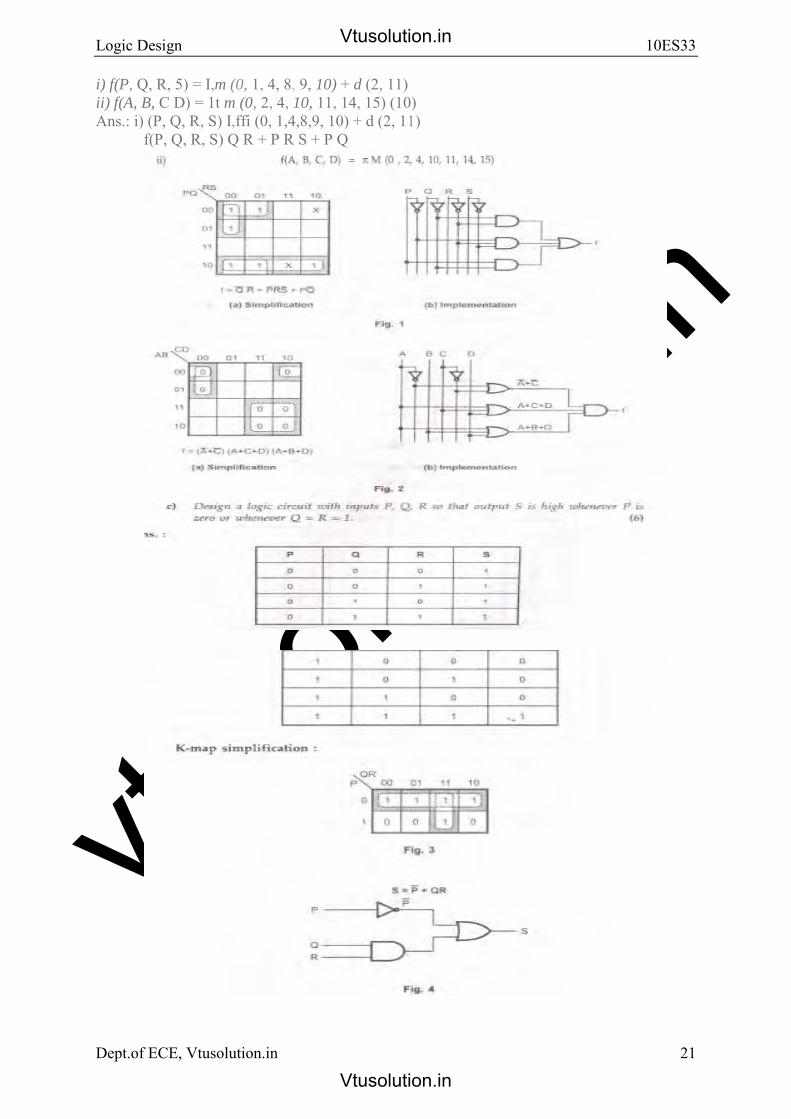
i) f(P, Q, R, 5) = I,m (0, 1, 4, 8, 9, 10) + d (2, 11)ii) f(A, B, C D) = 1t m (0, 2, 4, 10, 11, 14, 15) (10)Ans.: i) (P, Q, R, S) I,ffi (0, 1,4,8,9, 10) + d (2, 11)
f(P, Q, R, S) Q R + P R S + P Q
Vtusolution.in
Vtusolution.in

vtuso
lution
.in
Logic Design 10ES33
Dept.of ECE, Vtusolution.in 22
Aug 2008 Q.l a) Simplify the following expression using Kamaugh map. Implement the simpl~l.
circuit using the gates as indicated.
i) !(ABCD) = L m (2, 3, 4, 5, 13, 15) + Lex (8, 9, 10, 11) use only NAND gat~
ii) !(ABCD) = 1t (2, 3, 4, 6, 7, 10, 11, 12) use only NOR gates.
to implement these circuits.
i) f(ABCD) = L m (2, 3, 4, 5, 13, 15) + Lx (8, 9, la, 11)
Vtusolution.in
Vtusolution.in

vtuso
lution
.in
Logic Design 10ES33
Dept.of ECE, Vtusolution.in 23
Aug-2007
Vtusolution.in
Vtusolution.in
vtuso
lution
.in
Logic Design 10ES33
Dept.of ECE, Vtusolution.in 24
b) i) What are the advantage, disadvantages of K map?
ii) Simplify the following function in SOP form using K Map:
Sol. : i) Advantages of K-map method: 1. It provides a systematic approach for simplifying a Boolean expression.2. It is very convenient method for simplifying a Boolean expression upto sixvariables.Disadvantages of K-map method:1. As the number of variables increases it is difficult to make judgements aboutwhich combinations form the minimum expression. In case of complex
Vtusolution.in
Vtusolution.in

vtuso
lution
.in
Logic Design 10ES33
Dept.of ECE, Vtusolution.in 25
problem with 7, 8, or even 10 variables it is almost an impossible task to simplify expression by the mapping method.
Vtusolution.in
Vtusolution.in

vtuso
lution
.in
Logic Design 10ES33
Dept.of ECE, Vtusolution.in 26
Vtusolution.in
Vtusolution.in

vtuso
lution
.in
Logic Design 10ES33
Dept.of ECE, Vtusolution.in 27
Unit 2 Principles of combinational Logic-2
Hours-07
Quine-McCluskey minimization technique- Quine-McCluskey using don‟t care terms, educed Prime Implicant Tables, Map entered variables
Recommended readings:
1. John M Yarbrough, “Digital Logic Applications and Design”,Thomson Learning, 2001.
Unit- 3.5, 3.6
Vtusolution.in
Vtusolution.in

vtuso
lution
.in
Logic Design 10ES33
Dept.of ECE, Vtusolution.in 28
QUINE – McCLUSKEY METHOD Using K-maps for simplification of Boolean expressions with more than six
variables becomes a tedious and difficult task. Therefore a tabular method illustrate below can be used for the purpose. ALGORITHM FOR GENERATING PRIME IMPLICANTS The algorithm procedure is listed below 1.Express each minterm of the function in its binary representation.2. List the minterms by increasing index.3. Separate the sets of minterms of equal index with lines.4. Let i = 0.5. Compare each term of index I with each term of index I+1. For each pair of termsthat can combine which has only one bit position difference.6. Increase I by 1 and repeat step 5 . The increase of I continued until all terms arecompared. The new list containing all implicants of the function that have one lessvariable than those implicants in the generating list.7. Each section of the new list formed has terms of equal index. Steps 4,5, and 6 arerepeated on this list to form another list. Recall that two terms combine only if theyhave their dashes in the same relative positions and if they differ in exactly one bitposition.8. The process terminates when no new list is formed .9. All terms without check marks are prime implicants.Example: Find all the prime implicants of the functionf(w,x,y,z) = m(0,2,3,4,8,10,12,13,14)Step 1: Represent each minter in its 1-0 notation
no. minterm 1-0 notation index
0 2 3 4 8 10 12 13 14
w x y z w x y z w x y z w x y z w x y z w x y z w x y z w x y z w x y z
0 0 0 0 0 0 1 0 0 0 1 1 0 1 0 0 1 0 0 0 1 0 1 0 1 1 0 0 1 1 0 1 1 1 1 0
0 1 2 1 1 2 2 3 3
Vtusolution.in
Vtusolution.in

vtuso
lution
.in
Logic Design 10ES33
Dept.of ECE, Vtusolution.in 29
Step 2: List the minterm in increasing order of their index. No. w x y z index
0 2 4 8 3 10 12 13 14
0 0 0 0 0 0 1 0 0 1 0 0 1 0 0 0 0 0 1 1 1 0 1 0 1 1 0 0 1 1 0 1 1 1 1 0
Index 0
Index 1
Index 2
Index 3
W x y z index
0.2 0,4 0,8 2,3 2,10 4,12 8,10 8,12 10,14 12,13 12,14
0 0 – 0 0 – 0 0
- 0 0 00 0 1 –
- 0 1 0- 1 0 0
1 0 – 0 1 – 0 0 1 – 1 0 1 1 0 – 1 1 - 0
w x y z
(0, 2, 8, 10) (0, 4, 8,12 )
__ 0 __ 0 __ __ 0 0(index 0)
(8,10,12,14) 1__ __ 0 (index 1)
F(w,x,y,z)=x z + y z +w z+w x y +w x z
Vtusolution.in
Vtusolution.in

vtuso
lution
.in
Logic Design 10ES33
Dept.of ECE, Vtusolution.in 30
PETRICK’S METHOD OF DETERMINING IRREDUNDANT EXPRESSIONS FIND THE PRIME IMPLICANTS AND IRREDUNDANT EXPRESSION
F(W,X,Y,Z)= M(0,1,2,5,7,8,9,10,13,15) A=X Y , B= X Z C= Y Z D= X Z
P = (A+B)(A+C) (B)(C+D)(D)(A+B)(A+C)(B)(C+D)(D)
P = (A +C)(BD) = ABD +BCD F1(W,X,Y,Z)= ABD =X Y +X Z +X Z F2(W,X,Y,Z) = BCD = X Z + Y Z +X Z
DECIMAL METHOD FOR OBTAINING PRIME IMPLICANTS
The prime implicants can be obtained for decimal number represented minterms.In this procedure binary number are not used to find out prime implicants
f(w, x,y,z) =m(0,5,6,7,9,10,13,14,15) fsop= xy +xz+xyz+wyz+w x y z
MAP ENTERED VARIABLE(MEV)
It is graphical approach using k-map to have a variable of order n. Where in we are using a K-map of n-1 variable while map is entered with ouput function and variable.f(w,x,y.z) = m(2,3,4,5,13,15) +dc(8,9,10,11)Ans.fsop= w z +x y + w x y
karnaugh mapping is the best manual technique for boolean equation simplification,yet when the map sizes exceed five or six variable unwidely.
the technique called “map entered variables “ ( mevs ) increases the effective size ofa karnaugh maps, allowing a smaller map to handle a greater no. of variables
the map dimension and the no. of problem variables are related by 2n = m, wheren = no.of problem variable, m = no. of squares in k-maps. mev k-maps permit a cellto contain a single (x) or a complete switching expression, in addition to the 1s, 0sand don‟t care terms.
Vtusolution.in
Vtusolution.in

vtuso
lution
.in
Logic Design 10ES33
Dept.of ECE, Vtusolution.in 31
STEP:1 IF THE OUTPUT VARIABLE IS A “0” FOR BOTH STANDARD MINTERM COVERED
BY MEV MAP SQUARE, THEN A “0” IS WRITTEN IN THAT MEV MAP SQUARE.
STEP:2 IF THE OUTPUT VARIABLE IS “1” FOR BOTH STANDARD MINTERM COVERED BY MEV MAP SQUARE, THEN A “1” IS WRITTEN IN THAT MEV MAP SQUARE.
STEP:3 IF FOR THE MINTERMS COVERED BY THE MEV MAP SQUARE , THE OUTPUT VARIABLE HAS THE SAME VALUE AS THE MEV.
Vtusolution.in
Vtusolution.in

vtuso
lution
.in
Logic Design 10ES33
Dept.of ECE, Vtusolution.in 32
STEP:4 IF FOR THE STANDARD MINTERM COVERED BY A MEV MAP SQUARE, THE OUTPUT & MEV VARIABLES ARE COMPLIMENTS WRITE THE MEV
COMPLEMENT INTO MEV MAP SQUARE.
STEP:5 IF FOR STANDARD MINTERMS COVERED BY A MEV MAP SQUARE , THE OUTPUT VARIABLE IS A DON‟T CARE TERM, WRITE A DON‟T CARE SYMBOL “ x” INTO THE MEV MAP SQUARE.
STEP:6 IF FOR STANDARD MINTERMS COVERED BY A MEV MAP SQUARE , THE OUTPUT VARIABLE IS A DON‟T CARE TERM IN 1 CASE & “0” IN THE OTHER, WRITE “0” IF THE OUTPUT VARIABLE IS A DON‟T CARE TERM IN 1 CASE & “1” IN THE OTHER, WRITE “1”
Vtusolution.in
Vtusolution.in

vtuso
lution
.in
Logic Design 10ES33
Dept.of ECE, Vtusolution.in 33
TO READ THE SIMPLIFIED FUNCTION FROM A MEV K-MAP, FOLLOW THESE STEPS:
STEP:1 DETERMINE THE EPIs CONSISTING OF ONLY 1s ALONG WITH ANY DON‟T CARE
TERMS THAT MAY EXIST.{ i.e. COVER THE 1s IN K-MAP.}
STEP:2 CONSIDER THE 1s AS DON‟T CARE TERMS ONCE STEP 1 IS COMPLETED, BECAUSE ALL OF THE 1s HAVE BEEN PREVIOUSLY COVERED.
STEP:3 GROUP ALL THE IDENTICAL MEV TERMS WITH 1s OR DON‟T CARE TERMS TO MAXIMIZE THE MEV EPI SIZE. ANY MINTERM THAT ARE NOT CONTAINED IN THE MEV EPI ARE CONSIDERED TO BE 0s.{ i.e. COVER ALL THE MEVs IN THE K-MAP }
STEP:4 DETERMINE THE MEV EPIs BY READING THE K-MAP IN THE NORMAL FASHION. THEN “ AND ” THE MEV VARIABLE OR EXPRESSION WITH
THE REMAINING MAP VARIABLES.
Vtusolution.in
Vtusolution.in

vtuso
lution
.in
Logic Design 10ES33
Dept.of ECE, Vtusolution.in 34
Recommended question and answer –unit-2 Jan-2009
Q.2 a) Using Quine-Mcluskey method and prime implicant reduction table, obtain the
minimal sum expression for the Boolean function
F(w, x, y, z) = L mO, 4, 6, 7, 8,9, 10, 11, 15). .(12)
f(w, X, y, z) = L m (I, 4, 6, 7, 8, 9, 10, 11, 15)
:. f(w, x, y, z) = x y z + W x Z + W x + W x Y + x Y z + W Y z
b) Obtain the minimal product of the following Boolean functions using VEM technique:
f(w, x, y, z) = L m (1, 5, 7, 10, 11) + dc (2, 3, 6, 13) . (8) Ans. : f(w, x, y, z) = L m (1, 5, 7, 10, 11) + dc (2, 3, ,6, 13)Writing these rninterrns in SOP forills we get,
Now converting 4-variable terill into 3-variable terill we get, f(w, x, y, z) = illa z + ill1 Z + illl Z + ill2 Z + ill3 Z + ill3 Z + illS Z + illS Z + ill6 Z = illa Z + illl (z + z) + ill2 Z + ill3 (z + z) + illS (z + z) + ill6'Z
Applying grouping technique we get, f(w, x, y, z) = w Z + X Y + w Y + x y Z
Jan-2008
Vtusolution.in
Vtusolution.in

vtuso
lution
.in
Logic Design 10ES33
Dept.of ECE, Vtusolution.in 35
c. Simplify P = f(a, b, c) = L (0,1, 4, 5, 7) using two variable Karnaugh map. Write the
Boolean equation and realize using logic gates (8)
b) Simplify using Quine Mc Cluskey tabulation algorithm -
v = lea, b, c, d) = L (2, 3, 4, 5, 13, 15) + L d (8, 9, 10, 11)
(14)
Ans:
Vtusolution.in
Vtusolution.in

vtuso
lution
.in
Logic Design 10ES33
Dept.of ECE, Vtusolution.in 36
Vtusolution.in
Vtusolution.in

vtuso
lution
.in
Logic Design 10ES33
Dept.of ECE, Vtusolution.in 37
Final expression Y= AbC + bCd+ Bc +a B+ aD
Aug-2009
Q.2 a) Using Quine McCluskey method simplify the following function.
f (a, b, c, d) = Lm (0, 1, 2, 3, 8, 9)
Vtusolution.in
Vtusolution.in
vtuso
lution
.in
Logic Design 10ES33
38
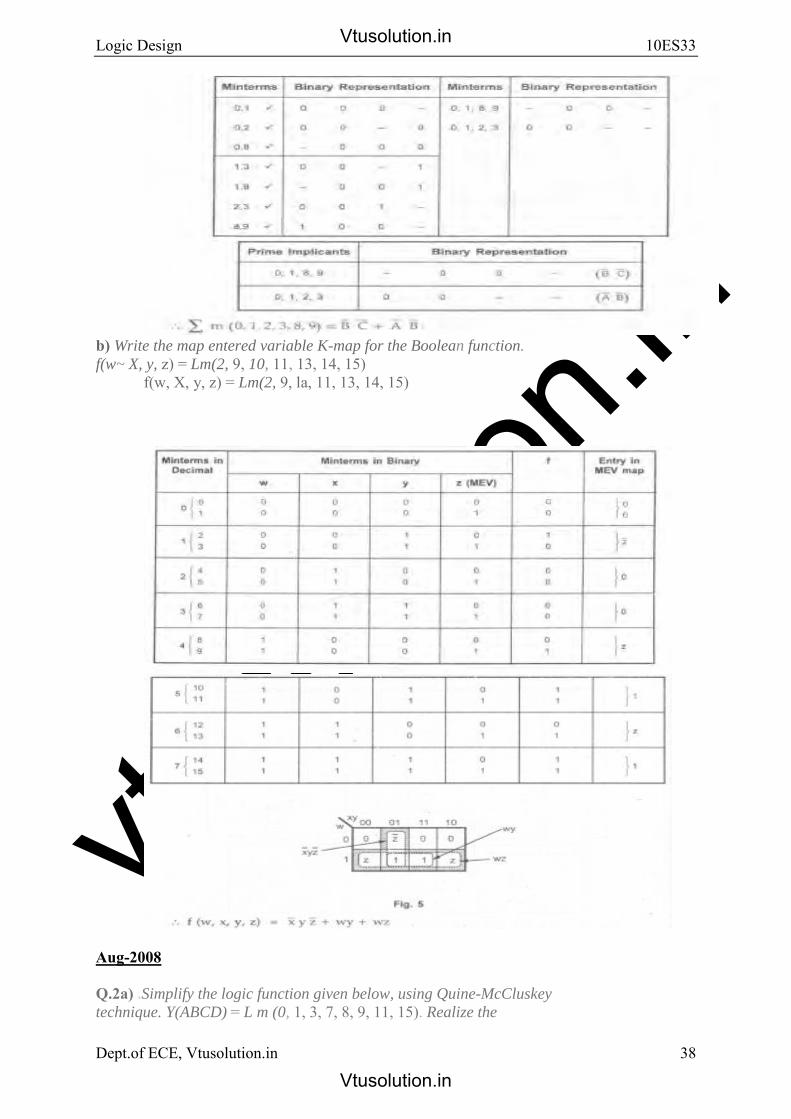
b) Write the map entered variable K-map for the Boolean function.
f(w~ X, y, z) = Lm(2, 9, 10, 11, 13, 14, 15)f(w, X, y, z) = Lm(2, 9, la, 11, 13, 14, 15)
Aug-2008
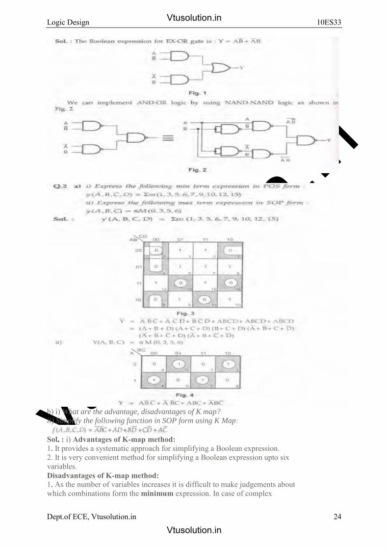
Q.2a) .Simplify the logic function given below, using Quine-McCluskey technique. Y(ABCD) = L m (0, 1, 3, 7, 8, 9, 11, 15). Realize the
Dept.of ECE, Vtusolution.in
Vtusolution.in
Vtusolution.in

vtuso
lution
.in
Logic Design 10ES33
Dept.of ECE, Vtusolution.in 39
expression using universal gates.
Vtusolution.in
Vtusolution.in

vtuso
lution
.in
Logic Design 10ES33
Dept.of ECE, Vtusolution.in 40
b) Simplify the logic function given below using variable - entered mapping (VEM)
technique. Y (ABeD) = L m (1, 3, 4, 5, 8, 9, 10, 15) + L d (2, 7, 11, 12, 13). (8)Ans. :1. Use A, B, C as ordinary K-map variable2. Make D the map-entered variable
Vtusolution.in
Vtusolution.in

vtuso
lution
.in
Logic Design 10ES33
Dept.of ECE, Vtusolution.in 41
Unit 3: 6 Hours
Analysis and design of combinational logic - I: General approach, Decoders-BCD decoders, Encoders
Recommended readings:
1. John M Yarbrough, “Digital Logic Applications and Design”,Thomson Learning, 2001.
Unit- 4.1, 4.3, 4.4
Vtusolution.in
Vtusolution.in

vtuso
lution
.in
Logic Design 10ES33
Dept.of ECE, Vtusolution.in 42
Decoder A Decoder is a multiple input ,multiple output logic circuit.The block diagram of a decoder is as shown below.
The most commonly used decoder is a n –to 2n decoder which ha n inputs and 2n
Output lines .
Vtusolution.in
Vtusolution.in

vtuso
lution
.in
Logic Design 10ES33
Dept.of ECE, Vtusolution.in 43
(6)
(2)
(3)
(4)
(5)
(7)
ENABLE
S E L E C T I/P
(10)
(14)
(13)
(12)
(11)
(15)
(9)
ENABLE
S E L E C T I/P
Vtusolution.in
Vtusolution.in
vtuso
lution
.in
Logic Design 10ES33
Dept.of ECE, Vtusolution.in 44
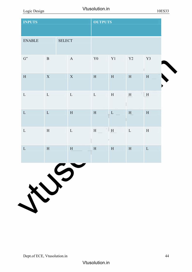
INPUTS OUTPUTS
ENABLE SELECT
G‟ B A Y0 Y1 Y2 Y3
H X X H H H H
L L L L H H H
L L H H L H H
L H L H H L H
L H H H H H L
Vtusolution.in
Vtusolution.in

vtuso
lution
.in
Logic Design 10ES33
Dept.of ECE, Vtusolution.in 45
(1) (7)
(2)
(3) (6)
(4)
(5)
(15)
(14)
(13)
(10)
(12)
(11)
(9)
Vtusolution.in
Vtusolution.in

vtuso
lution
.in
Logic Design 10ES33
Dept.of ECE, Vtusolution.in 46
3-to-8 decoder logic diagram
Y0
Y4
Y5
Y7
Y6
Y2
Y3
Y1
Y5
Y7
Y6
Y3
Y1 Y0
Y2
Y4
A
B
C
A
B
C
A
B
A
B
G1
G2
G2
G2
G2
G1
z.H
y.H
w.H
x.H
EN.L
ENABLE
1
3
6
4
5
2
13
14
15
10
11
12
8
9
1
3
6
4
5
2
13
14
15
11
12
8
9 10
D0.L
D2.L
D3.L
D4.L
D5.L
D6.L
D7.L
D1.L
D0.L
D2.L
D3.L
D4.L
D5.L
D6.L
D7.L
D1.L
1 OF 16 DATA OUTPUTS
Vtusolution.in
Vtusolution.in

vtuso
lution
.in
Logic Design 10ES33
Dept.of ECE, Vtusolution.in 47
In this realization shown above the three inputs are assigned x0,x1,and x2, and the eight outputs are Z0 to Z7.
Function specifc decoders also exist which have less than 2n outputs . examples are 8421code decoder also called BCD to decimal decoder. Decoders that drive seven segment displays also exist.
Realization of boolean expression using Decoder and OR gate
We see from the above truth table that the output expressions corrwespond to a single minterm. Hence a n –to 2n decoder is a minterm generator. Thus by using OR gates inconjunction with a a n –to 2n decoder boolean function realization is possible.Ex: to realize the Boolean functions given below using decoders… •F1=Σm(1,2,4,5)•F2=Σm(1,5,7)
Priority encoder 8-3 line priority encoder
In priority encoder a priority scheme is assigned to the input lines so that whenever more than one input line is asserted at any time, the output is determined by the input line having the highest priority.
The Valid bit is used to indicate that atleast one inut line is asserted. This is done to distinguish the situation that no input line is asserted from when the X0 input line is asserted , since in both cases Z1Z2Z3 =000.
Vtusolution.in
Vtusolution.in

vtuso
lution
.in
Logic Design 10ES33
Dept.of ECE, Vtusolution.in 48
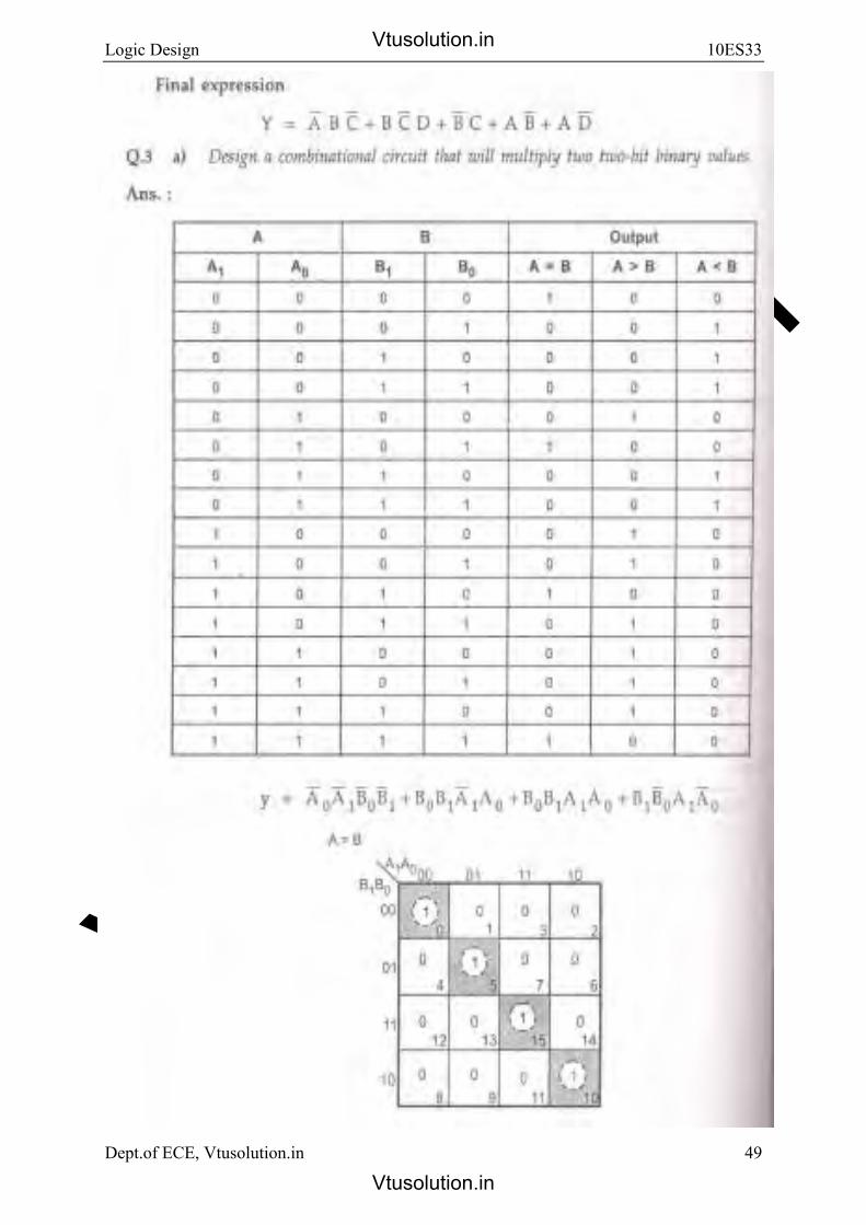
Recommended question and answer –unit-3 Jan 2009 Q.3 a) Realize the following functions expressed in maxterm canonical form in two possible
ways using 3-8 line and decoder :
b) What are the problems associated with the basic encoder? Explain, how can these
problems be overcome by priority encoder, considering 8 input lines. (10)
Ans. : The basic encoder has ambiguity that when all inputs are Osth~ outputs are Os. The zero output can also be generated when Do = 1. This amb:guity can be resolved by providing an additional output that specifies the valid condition.
A priority encoder is an encoder circuit that indicates the priority function. In priority encoder, if two or more inputs are equal to 1 at the same time, the inputs having the highest priority will take precedence. Also, the output V (valid output indicator) indicates one or more of the inputs are equal to 1. If all inputs are '0', V is equal to b and other two outputs of the circuit are not used. Jan 2008
Vtusolution.in
Vtusolution.in
vtuso
lution
.in
Logic Design 10ES33
Dept.of ECE, Vtusolution.in 49
Vtusolution.in
Vtusolution.in

vtuso
lution
.in
Logic Design 10ES33
Dept.of ECE, Vtusolution.in 50
Vtusolution.in
Vtusolution.in
vtuso
lution
.in
Logic Design 10ES33
Dept.of ECE, Vtusolution.in 51
Aug 2009
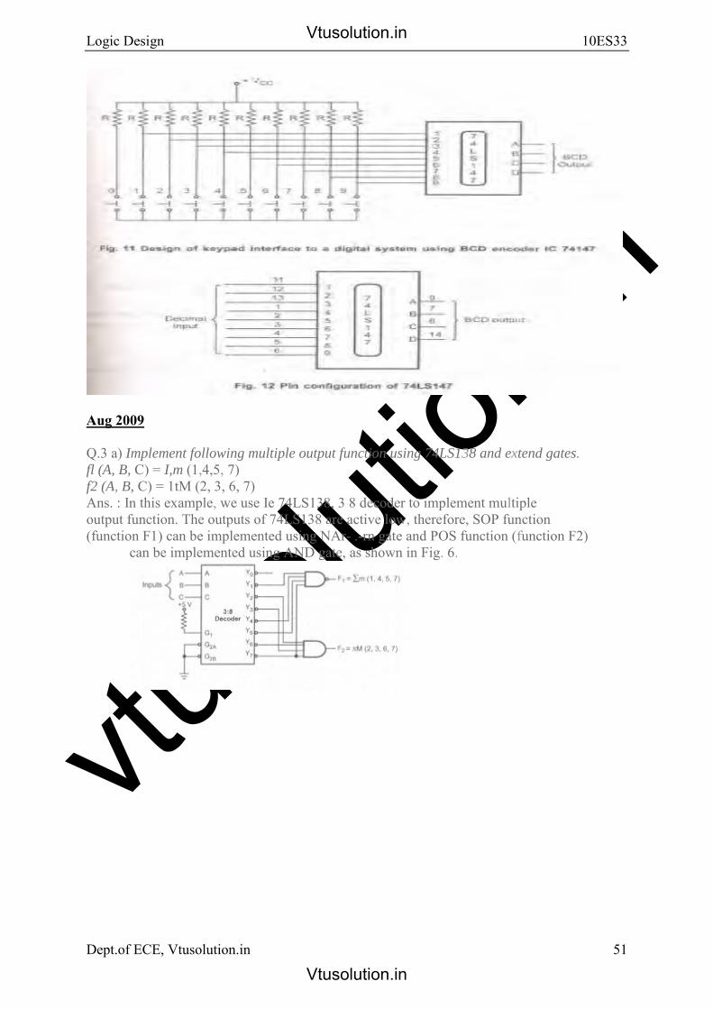
Q.3 a) Implement following multiple output function using 74LS138 and extend gates.
fl (A, B, C) = I,m (1,4,5, 7)f2 (A, B, C) = 1tM (2, 3, 6, 7)Ans. : In this example, we use Ie 74LS138, 3 8 decoder to implement multipleoutput function. The outputs of 74LS138 are active low, therefore, SOP function(function F1) can be implemented using NAr-..-rn gate and POS function (function F2)
can be implemented using AND gate, as shown in Fig. 6.
Vtusolution.in
Vtusolution.in

vtuso
lution
.in
Logic Design 10ES33
Dept.of ECE, Vtusolution.in 52
Ans. : An encoder is a digital circuit that performs the inverse operation of. a decoder. An encoder has 2n (or fewer) input lines and n output lines: In encoder the
output lines generate the binary code corresponding to the input value. The Fig. 8 shows the general structure of the encoder circuit. As shown in the Fig. 8, the decoded information is presented as 2n inputs producing n
possible outputs.
Aug-2007
Vtusolution.in
Vtusolution.in

vtuso
lution
.in
Logic Design 10ES33
Dept.of ECE, Vtusolution.in 53
Vtusolution.in
Vtusolution.in

vtuso
lution
.in
Logic Design 10ES33
Dept.of ECE, Vtusolution.in 54
Vtusolution.in
Vtusolution.in

vtuso
lution
.in
Logic Design 10ES33
Dept.of ECE, Vtusolution.in 55
Unit 4: Analysis and design of combinational logic - II: 6 Hours
Digital multiplexers-Using multiplexers as Boolean function generators. Adders and subtractors - Cascading full adders, Look ahead carry, Binary comparators
Recommended readings:
1. John M Yarbrough, “Digital Logic Applications and Design”,Thomson Learning, 2001.
Units- 4.5, 4.6 - 4.6.1, 4.6.2, 4.7
Vtusolution.in
Vtusolution.in

vtuso
lution
.in
Logic Design 10ES33
Dept.of ECE, Vtusolution.in 56
The Multiplexer
The Multiplexer which sometimes are simply called "Mux" or "Muxes", are devices that act like a very fast acting rotary switch. They connect multiple input lines 2, 4, 8, 16 etc one at a time to a common output line and are used as one method of reducing the number of logic gates required in a circuit. Multiplexers are individual Analogue Switches as opposed to the "mechanical" types such as normal conventional switches and relays. They are usually made from MOSFETs devices encased in a single package and are controlled using standard logic gates. An example of a Multiplexer is shown below.
4-to-1 Channel Multiplexer
Addressing Input Selected b a
0 0 A 0 1 B 1 0 C 1 1 D
The Boolean expression for this 4 to 1 Multiplexer is given as:
Q = abA + abB + abC + abD
In this example at any instant in time only one of the four analogue switches is closed, connecting only one of the input lines A to D to the single output at Q. As to which switch is closed depends upon the addressing input code on lines "a" and "b", so for this example to select input B to the output at Q, the binary input address would need to be "a" = logic "1" and "b" = logic "0". Adding more control address lines will allow the multiplexer to control more inputs. Multiplexers can also be used to switch either analogue, digital or video signals, with the switching current in analogue circuits limited to below 10mA to 20mA per channel in order to reduce heat dissipation.
Multiplexers are not limited to just switching a number of different input lines or channels to one common single output. There are also types that can switch their inputs to multiple outputs and have arrangements or 4 to 2, 8 to 3 or even 16 to 4 etc configurations and an example of a simple Dual channel 4 input multiplexer (4 to 2) is given below:
Vtusolution.in
Vtusolution.in

vtuso
lution
.in
Logic Design 10ES33
Dept.of ECE, Vtusolution.in 57
4-to-2 Channel Multiplexer
Here in this example the 4 input channels are switched to 2 individual output lines but larger arrangements are also possible. This simple 4 to 2 configuration could be used for example, to switch audio signals for stereo pre-amplifiers or mixers.
The De-multiplexer
De-multiplexers or "De-muxes", are the exact opposite of the Multiplexers we saw in the previous tutorial in that they have one single input data line and then switch it to any one of their individual multiple output lines one at a time. The De-multiplexer converts the serial data signal at the input to a parallel data at its output lines as shown below.
1-to-4 Channel De-multiplexer
Addressing Output Selected b a
0 0 A 0 1 B 1 0 C 1 1 D
The Boolean expression for this De-multiplexer is given as:
F = ab A + abB + abC + abD
Vtusolution.in
Vtusolution.in

vtuso
lution
.in
Logic Design 10ES33
Dept.of ECE, Vtusolution.in 58
The function of the De-multiplexer is to switch one common data input line to any one of the 4 output data lines A to D in our example above. As with the multiplexer the individual solid state switches are selected by the binary input address code on the output select pins "a" and "b" and by adding more address line inputs it is possible to switch more outputs giving a 1-to-2n data lines output. Some standard De-multiplexer IC´s also have an "enable output" input pin which disables or prevents the input from being passed to the selected output. Also some have latches built into their outputs to maintain the output logic level after the address inputs have been changed. However, in standard decoder type circuits the address input will determine which single data output will have the same value as the data input with all other data outputs having the value of logic "0".
Standard De-multiplexer IC packages available are the TTL 74LS138 1 to 8-output De-multiplexer, theTTL 74LS139 Dual 1 to 4-output De-multiplexer or the CMOS CD4514 1 to 16-output De-multiplexer. Another type of De-multiplexer is the 24-pin, 74LS154 which is a 4-bit to 16-line De-multiplexer/decoder. Here the output positions are selected using the 4-bit binary coded input.
Combination Logic
Unlike Sequential Logic circuits whose outputs are dependant on both the present input and their previous output state giving them some form of Memory, the outputs of Combinational Logic circuits are only determined by their current input state as they have no feedback, and any changes to the signals being applied to their inputs will immediately have an effect at the output. In other words, in a Combination Logic circuit, if the input condition changes state so too does the output as combinational circuits have No Memory.
Combination Logic circuits are made up from basic logic AND, OR or NOT gates that are "combined" or connected together to produce more complicated switching circuits.
As combination logic circuits are made up from individual logic gates they can also be considered as "decision making circuits" and combinational logic is about combining logic gates together to process two or more signals in order to produce at least one output signal according to the logical function of each logic gate. Common combinational circuits made up from individual logic gates include Multiplexers, Decoders and De-multiplexers, Full and Half Adders etc.
Vtusolution.in
Vtusolution.in

vtuso
lution
.in
Logic Design 10ES33
Dept.of ECE, Vtusolution.in 59
Classification of Combinational Logic
One of the most common uses of combination logic is in Multiplexer and De-multiplexer type circuits. Here, multiple inputs or outputs are connected to a common signal line and logic gates are used to decode an address to select a single data input or output switch. A multiplexer consist of two separate components, a logic decoder and some solid state switches, but before we can discuss multiplexers, decoders and de-multiplexers in more detail we first need to understand how these devices use these "solid state switches" in their design.
The Encoder
Unlike a multiplexer that selects one individual data input line and then sends that data to a single output line or switch, an Encoder takes all the data inputs one at a time and converts them to a single encoded output. Then, it is a multi-input data line, combinational logic circuit that converts the logic level "1" data at its inputs to an equivalent binary code at its output. Generally encoders produce outputs of 2-bit, 3-bit or 4-bit codes depending upon the number of data input lines and a "n-bit" encoder has 2n input lines with common types that include 4-to-2, 8-to-3 and 16-to-4 line configurations. Encoders are available to encode either a decimal or hexadecimal input pattern to typically a binary or B.C.D. output code.
4-to-2 Bit Encoder
Vtusolution.in
Vtusolution.in

vtuso
lution
.in
Logic Design 10ES33
Dept.of ECE, Vtusolution.in 60
One of the main disadvantages of standard encoders is that they can generate the wrong output code when there is more than one input present at logic level "1". For example, if we make inputs D1 and D2 HIGH at logic "1" at the same time, the resulting output is neither at "01" or at "10" but will be at "11" which is an output code that is different to the actual input present. One simple way to overcome this problem is to "Prioritize" the level of each input pin and if there was more than one input at logic level "1" the actual output code would only correspond to the input with the highest designated priority. Then this type of encoder are known as Priority Encoders or P-encoder.
Priority Encoders
Priority Encoders come in many forma and an example of an 8-input Priority Encoder along with its truth table is as shown below.
8-to-3 Bit Priority Encoder
Priority encoders are available in standard IC form and the TTL 74LS148 is an 8 to 3 bit priority encoder which has eight active LOW (logic "0") inputs and provides a 3-bit code of the highest ranked input at its output. Priority encoders output the highest order input first for example, if input lines "D2", "D3" and "D5" are applied simultaneously the output code would be for input "D5" ("101") as this has the highest order out of the 3 inputs. Once input "D5" had been removed the next highest output code would be for input "D3" ("011"), and so on.
Encoder Applications
Keyboard Encoders
Priority encoders can be used to reduce the number of wires needed in circuits or applications that has multiple inputs. For example, assume that a microcomputer needs to read the 104 keys of a standard QWERTY keyboard where only one key would be pressed or HIGH at any one time. One way would be to connect all 104 wires from the keys directly to the computer but this would be impractical for a small home PC, but another better way would be to use an
Vtusolution.in
Vtusolution.in

vtuso
lution
.in
Logic Design 10ES33
Dept.of ECE, Vtusolution.in 61
encoder. The 104 individual buttons or keys could be encoded into a standard ASCII code of only 7-bits (0 to 127 decimal) to represent each key or character and then inputted as a much smaller 7-bit B.C.D code directly to the computer. Keypad encoders such as the 74C923 20-key encoder are available.
Positional Encoders
Another more common application is in magnetic positional control as used on ships or robots etc. Here the angular or rotary position of a compass is converted into a digital code by an encoder and inputted to the systems computer to provide navigational data and an example of a simple 8 position to 3-bit output compass encoder is shown below.
Compass Direction Binary Output Q0 Q1 Q2
North 0 0 0 North-East 0 0 1
East 0 1 0 South-East 0 1 1
South 1 0 0 South-West 1 0 1
West 1 1 0 North-West 1 1 1
Interrupt Requests
Other applications for Priority Encoders may include detecting interrupts in microprocessor applications. Here the microprocessor uses interrupts to allow peripheral devices such as the disk drive, scanner, mouse, or printer etc, to communicate with it, but the microprocessor can only "talk" to one peripheral device at a time. The processor uses "Interrupt Requests" or "IRQ" signals to assign priority to the devices to ensure that the most important peripheral device is serviced first. The order of importance of the devices will depend upon their connection to the priority encoder.
Because implementing such a system using priority encoders such as the standard 74LS148 priority encoder IC involves additional logic circuits, purpose built integrated circuits such as the 8259 Programmable Priority Interrupt Controller is available.
Vtusolution.in
Vtusolution.in
vtuso
lution
.in
Logic Design 10ES33
Dept.of ECE, Vtusolution.in 62
IRQ Number Typical Use Description IRQ 0 System timer Internal System Timer. IRQ 1 Keyboard Keyboard Controller. IRQ 3 COM2 & COM4 Second and Fourth Serial Port. IRQ 4 COM1 & COM3 First and Third Serial Port. IRQ 5 Sound Sound Card. IRQ 6 Floppy disk Floppy Disk Controller. IRQ 7 Parallel port Parallel Printer. IRQ 12 Mouse PS/2 Mouse. IRQ 14 Primary IDE Primary Hard Disk Controller. IRQ 15 Secondary IDE Secondary Hard Disk Controller.
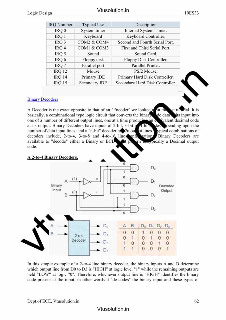
Binary Decoders
A Decoder is the exact opposite to that of an "Encoder" we looked at in the last tutorial. It is basically, a combinational type logic circuit that converts the binary code data at its input into one of a number of different output lines, one at a time producing an equivalent decimal code at its output. Binary Decoders have inputs of 2-bit, 3-bit or 4-bit codes depending upon the number of data input lines, and a "n-bit" decoder has 2n output lines. Typical combinations of decoders include, 2-to-4, 3-to-8 and 4-to-16 line configurations. Binary Decoders are available to "decode" either a Binary or BCD input pattern to typically a Decimal output code.
A 2-to-4 Binary Decoders.
In this simple example of a 2-to-4 line binary decoder, the binary inputs A and B determine which output line from D0 to D3 is "HIGH" at logic level "1" while the remaining outputs are held "LOW" at logic "0". Therefore, whichever output line is "HIGH" identifies the binary code present at the input, in other words it "de-codes" the binary input and these types of
Vtusolution.in
Vtusolution.in

vtuso
lution
.in
Logic Design 10ES33
Dept.of ECE, Vtusolution.in 63
binary decoders are commonly used as Address Decoders in microprocessor memory applications.
Memory Address Decoder.
In modern microprocessor systems the amount of memory required can be quite high and is generally more than one single memory chip alone. One method of overcoming this problem is to connect lots of individual memory chips together and to read the data on a common "Data Bus". In order to prevent the data being "read" from each memory chip at the same time, each memory chip is selected individually one at time and this process is known as Address Decoding.
Each memory chip has an input called Chip Select or CS which is used by the MPU to select the appropriate memory chip and a logic "1" on this input selects the device and a logic "0" on the input de-selects it. By selecting or de-selecting each chip, allows us to select the correct memory device for a particular address and when we specify a particular memory address, the corresponding memory location exists ONLY in one of the chips.
For example, Lets assume we have a very simple microprocessor system with only 1Kb of RAM memory and 10 address lines. The memory consists of 128x8-bit (128x8 = 1024 bytes) devices and for 1Kb we will need 8 individual memory devices but in order to select the correct memory chip we will also require a 3-to-8 line binary decoder as shown below.
Memory Address Decoding.
The binary decoder requires 3 address lines, (A0 to A2) to select each one of the 8 chips (the lower part of the address), while the remaining 7 address lines (A3 to A9) select the correct memory location on that chip (the upper part of the address). Having selected a memory location using the address bus, the information at the particular internal memory location is sent to the "Data Bus" for use by the microprocessor. This is of course a simple example but the principals remain the same for all types of memory chips or modules.
Vtusolution.in
Vtusolution.in

vtuso
lution
.in
Logic Design 10ES33
Dept.of ECE, Vtusolution.in 64
Binary Decoders are very useful devices for converting one digital format to another, such as binary or BCD type data into decimal or octal etc and commonly available decoder IC's are the TTL 74LS138 3-to-8 line binary decoder or the 74ALS154 4-to-16 line decoder. They are also very useful for interfacing to 7-segment displays such as the TTL 74LS47 which we will look at in the next tutorial.
Display Decoders
A Decoder IC, is a device which converts one digital format into another and the most commonly used device for doing this is the BCD (Binary Coded Decimal) to 7-Segment Display Decoder. 7-segment LED (Light Emitting Diode) or LCD (Liquid Crystal) Displays, provide a very convenient way of displaying information or digital data in the form of Numbers, Letters or even Alpha-numerical characters and they consist of 7 individual LEDs (the segments), within one single display package. In order to produce the required numbers or characters from 0 to 9 and A to F respectively, on the display the correct combination of LED segments need to be illuminated and Display Decoders do just that. A standard 7-segment LED or LCD display generally has 8 input connections, one for each LED segment and one that acts as a common terminal or connection for all the internal segments. Some single displays have an additional input pin for the decimal point in their lower right or left hand corner.
There are two important types of 7-segment LED digital display.
The Common Cathode Display (CCD) - In the common cathode display, all the cathodeconnections of the LEDs are joined together to logic "0" and the individual segments areilluminated by application of a "HIGH", logic "1" signal to the individual Anodeterminals.
The Common Anode Display (CAD) - In the common anode display, all the anodeconnections of the LEDs are joined together to logic "1" and the individual segments areilluminated by connecting the individual Cathode terminals to a "LOW", logic "0"signal.
7-Segment Display Format
Truth Table for a 7-segment display
Individual Segments Display a b c d e f g × × × × × × 0
× × 1 × × × × × 2
Individual Segments Display a b c d e f g × × × × × × × 8 × × × × × 9 × × × × × × A
Vtusolution.in
Vtusolution.in

vtuso
lution
.in
Logic Design 10ES33
Dept.of ECE, Vtusolution.in 65
× × × × × 3 × × × × 4
× × × × × 5 × × × × × × 6 × × × 7
× × × × × b × × × × C
× × × × × d × × × × × E × × × × F
.
It can be seen that to display any single digit number from 0 to 9 or letter from A to F, we would need 7 separate segment connections plus one additional connection for the LED's "common" connection. Also as the segments are basically a standard light emitting diode, the driving circuit would need to produce up to 20mA of current to illuminate each individual segment and to display the number 8, all 7 segments would need to be lit resulting a total current of nearly 140mA, (8 x 20mA). Obviously, the use of so many connections and power consumption is impractical for some electronic or microprocessor based circuits and so in order to reduce the number of signal lines required to drive just one single display, display decoders such as the BCD to 7-Segment Display Decoder and Driver IC's are used instead.
Binary Coded Decimal
Binary Coded Decimal (BCD or "8421" BCD) numbers are made up using just 4 data bits (a nibble or half a byte) similar to the Hexadecimal numbers we saw in the binary tutorial, but unlike hexadecimal numbers that range in full from 0 through to F, BCD numbers only range from 0 to 9, with the binary number patterns of 1010 through to 1111 (A to F) being invalid inputs for this type of display and so are not used as shown below.
Decimal Binary Pattern BCD 8 4 2 1 0 0 0 0 0 0 1 0 0 0 1 1 2 0 0 1 0 2 3 0 0 1 1 3 4 0 1 0 0 4 5 0 1 0 1 5 6 0 1 1 0 6 7 0 1 1 1 7
Decimal Binary Pattern BCD 8 4 2 1 8 1 0 0 0 8 9 1 0 0 1 9 10 1 0 1 0 Invalid 11 1 0 1 1 Invalid 12 1 1 0 0 Invalid 13 1 1 0 1 Invalid 14 1 1 1 0 Invalid 15 1 1 1 1 Invalid
BCD to 7-Segment Display Decoders
A binary coded decimal (BCD) to 7-segment display decoder such as the TTL 74LS47 or 74LS48, have 4 BCD inputs and 7 output lines, one for each LED segment. This allows a smaller 4-bit binary number (half a byte) to be used to display all the denary numbers from 0
Vtusolution.in
Vtusolution.in

vtuso
lution
.in
Logic Design 10ES33
Dept.of ECE, Vtusolution.in 66
to 9 and by adding two displays together, a full range of numbers from 00 to 99 can be displayed with just a single byte of 8 data bits.
BCD to 7-Segment Decoder
The use of packed BCD allows two BCD digits to be stored within a single byte (8-bits) of data, allowing a single data byte to hold a BCD number in the range of 00 to 99.
An example of the 4-bit BCD input (0100) representing the number 4 is given below.
Example No1
In practice current limiting resistors of about 150Ω to 220Ω would be connected in series between the decoder/driver chip and each LED display segment to limit the maximum current flow. Different display decoders or drivers are available for the different types of display available, e.g. 74LS48 for common-cathode LED types, 74LS47 for common-anode LED types, or the CMOS CD4543 for liquid crystal display (LCD) types.
Liquid crystal displays (LCD´s) have one major advantage over similar LED types in that they consume much less power and nowadays, both LCD and LED displays are combined
Vtusolution.in
Vtusolution.in

vtuso
lution
.in
Logic Design 10ES33
Dept.of ECE, Vtusolution.in 67
together to form larger Dot-Matrix Alphanumeric type displays which can show letters and characters as well as numbers in standard Red or Tri-colour outputs.
The Binary Adder
Another common and very useful combinational logic circuit is that of the Binary Adder circuit. The Binary Adder is made up from standard AND and Ex-OR gates and allow us to "add" single bits of data together to produce two outputs, the SUM ("S") of the addition and a CARRY ("C"). One of the main uses for the Binary Adder is in arithmetic and counting circuits.
Consider the addition of two denary (base 10) numbers below.
123 A (Augend) + 789 B (Addend) 912 SUM
Each column is added together starting from the right hand side. As each column is added together a carry is generated if the result is greater or equal to ten, the base number. This carry is then added to the result of the addition of the next column to the left and so on, simple school math's addition. Binary addition is based on similar principals but a carry is only generated when the result in any column is greater or equal to "2", the base number of binary.
Binary Addition
Binary Addition follows the same basic rules as for the denary addition above except in binary there are only two digits and the largest digit is "1", so any "SUM" greater than 1 will result in a "CARRY". This carry 1 is passed over to the next column for addition and so on. Consider the single bit addition below.
0 0 1 1 + 0 + 1 + 0 + 1
0 1 1 10
The single bits are added together and "0 + 0", "0 + 1", or "1 + 0" results in a sum of "0" or "1" until you get to "1 + 1" then the sum is equal to "2". For a simple 1-bit addition problem like this, the resulting carry bit could be ignored which would result in an output truth table resembling that of an Ex-OR Gate as seen in the Logic Gates section and whose result is the sum of the two bits but without the carry. An Ex-OR gate only produces an output "1" when either input is at logic "1", but not both. However, all microprocessors and electronic calculators require the carry bit to correctly calculate the equations so we need to rewrite them to include 2 bits of output data as shown below.
00 00 01 01 + 00 + 01 + 00 + 01
00 01 01 10
Vtusolution.in
Vtusolution.in
vtuso
lution
.in
Logic Design 10ES33
Dept.of ECE, Vtusolution.in 68
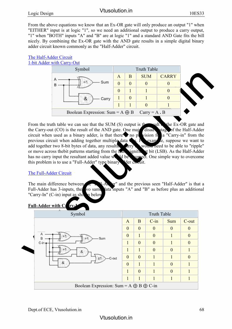
From the above equations we know that an Ex-OR gate will only produce an output "1" when "EITHER" input is at logic "1", so we need an additional output to produce a carry output, "1" when "BOTH" inputs "A" and "B" are at logic "1" and a standard AND Gate fits the bill nicely. By combining the Ex-OR gate with the AND gate results in a simple digital binary adder circuit known commonly as the "Half-Adder" circuit.
The Half-Adder Circuit 1-bit Adder with Carry-Out
Symbol Truth Table A B SUM CARRY 0 0 0 0 0 1 1 0 1 0 1 0 1 1 0 1
Boolean Expression: Sum = A ⊕ B Carry = A . B
From the truth table we can see that the SUM (S) output is the result of the Ex-OR gate and the Carry-out (CO) is the result of the AND gate. One major disadvantage of the Half-Adder circuit when used as a binary adder, is that there is no provision for a "Carry-in" from the previous circuit when adding together multiple data bits. For example, suppose we want to add together two 8-bit bytes of data, any resulting carry bit would need to be able to "ripple" or move across thebit patterns starting from the least significant bit (LSB). As the Half-Adder has no carry input the resultant added value would be incorrect. One simple way to overcome this problem is to use a "Full-Adder" type binary adder circuit.
The Full-Adder Circuit
The main difference between the "Full-Adder" and the previous seen "Half-Adder" is that a Full-Adder has 3-inputs, the two same data inputs "A" and "B" as before plus an additional "Carry-In" (C-in) input as shown below.
Full-Adder with Carry-In
Symbol Truth Table A B C-in Sum C-out0 0 0 0 0 0 1 0 1 0 1 0 0 1 0 1 1 0 0 1 0 0 1 1 0 0 1 1 0 1 1 0 1 0 1 1 1 1 1 1
Boolean Expression: Sum = A ⊕ B ⊕ C-in
Vtusolution.in
Vtusolution.in

vtuso
lution
.in
Logic Design 10ES33
Dept.of ECE, Vtusolution.in 69
The Full-Adder circuit above consists of three Ex-OR gates, two AND gates and an OR gate. The truth table for the Full-Adder includes an additional column to take into account the Carry-in input as well as the summed output and Carry-out. 4-bit Full-Adder circuits are available as standard IC packages in the form of the TTL 74LS83 or the 74LS283 which can add together two 4-bit binary numbers and generate a SUM and a CARRY output.
The Digital Comparator
Another common and very useful combinational logic circuit is that of the Digital Comparator circuit. Digital or Binary Comparators are made up from standard AND, NOR and NOT gates that compare the digital signals at their input terminals and produces an output depending upon the condition of the inputs. For example, whether input A is greater than, smaller than or equal to input B etc.
Digital Comparators can compare a variable or unknown number for example A (A1, A2, A3, .... An, etc) against that of a constant or known value such as B (B1, B2, B3, .... Bn, etc) and produce an output depending upon the result. For example, a comparator of 1-bit, (A and B) would produce the following three output conditions.
This is useful if we want to compare two values and produce an output when the condition is achieved. For example, produce an output from a counter when a certain count number is reached. Consider the simple 1-bit comparator below.
1-bit Comparator
Then the operation of a 1-bit digital comparator is given in the following Truth Table.
Truth Table
Inputs Outputs B A A > B A = B A < B 0 0 0 1 0 0 1 1 0 0 1 0 0 0 1 1 1 0 1 0
You may notice two distinct features about the comparator from the above truth table. Firstly, the circuit does not distinguish between either two "0" or two "1"'s as an output A = B is
Vtusolution.in
Vtusolution.in

vtuso
lution
.in
Logic Design 10ES33
Dept.of ECE, Vtusolution.in 70
produced when they are both equal, either A = B = "0" or A = B = "1". Secondly, the output condition for A = B resembles that of a commonly available logic gate, the Exclusive-NOR or Ex-NOR gate giving Q = A ⊕ B
Digital comparators actually use Exclusive-NOR gates within their design for comparing the respective pairs of bits in each of the two words with single bit comparators cascaded together to produce Multi-bit comparators so that larger words can be compared.
Magnitude Comparators
As well as comparing individual bits, multi-bit comparators can be constructed to compare whole binary or BCD words to produce an output if one word is larger, equal to or less than the other. A very good example of this is the 4-bit Magnitude Comparator. Here, two 4-bit words ("nibbles") are compared to produce the relevant output with one word connected to inputs A and the other to be compared against connected to input B as shown below.
4-bit Magnitude Comparator
Some commercially available Magnitude Comparators such as the 7485 have additional input terminals that allow more individual comparators to be "cascaded" together to compare words larger than 4-bits with magnitude comparators of "n"-bits being produced. These cascading inputs are connected directly to the corresponding outputs of the previous comparator as shown to compare 8, 16 or even 32-bit words.
Vtusolution.in
Vtusolution.in

vtuso
lution
.in
Logic Design 10ES33
71
8-bit Word Comparator
Designing a circuit that adds three 4-bit numbers Recall that a 4-bit binary adder adds two binary numbers, where each number is of 4 bits. For adding three 4-bit numbers we have: Inputs _ First 4-bit number X = X3X2X1X0 _ Second 4-bit number Y = Y3Y2Y1Y0 _ Third 4-bit number Z = Z3Z2Z1Z0 Outputs The summation of X, Y, and Z. How many output lines are exactly needed will be discussed as we proceed. To design a circuit using MSI devices that adds three 4-bit numbers, we first have to understand how the addition is done. In this case, the addition will take place in two steps, that is, we will first add the first two numbers, and the resulting sum will be added to the third number, thus giving us the complete addition. Apparently it seems that we will have to use two 4-bit adders, and probably some extra hardware as well. Let us analyze the steps involved in adding three 4-bit numbers. Step 1: Addition of X and Y A 4-bit adder is required. This addition will result in a sum and a possible carry, as follows:
X3X2X1X0
Dept.of ECE, Vtusolution.in
Vtusolution.in
Vtusolution.in

vtuso
lution
.in
Logic Design 10ES33
Dept.of ECE, Vtusolution.in 72
Y3Y2Y1Y0 ----------------- C4 S3S2S1S0 Note that the input carry Cin = 0 in this 4-bit adder
Step 2: Addition of S and Z This resulting partial sum (i.e. S3S2S1S0) will be added to the third 4-bit number Z3Z2Z1Z0 by using another 4-bit adder as follows, resulting in a final sum and a possible carry: S3S2S1S0 Z3Z2Z1Z0 ----------------- D4 F3F2F1F0
where F3F2F1F0 represents the final sum of the three inputs X, Y, and Z. Again, in this step, the input carry to this second adder will also be zero. Notice that in Step 1, a carry C4 was generated in bit position 4, while in Step 2, another carry D4 was generated also in bit position 4. These two carries must be added together to generate the final Sum bits of positions 4 and 5 (F4 and F5). Adding C4 and D4 requires a half adder. Thus, the output from this circuit will be six bits, namely F5 F4 F3F2F1F0 (See Figure )
Figure : Circuit for adding three 4-bit numbers
Design a 4-to-16 Decoder using five 2-to-4 Decoders with enable inputs
Vtusolution.in
Vtusolution.in

vtuso
lution
.in
Logic Design 10ES33
Dept.of ECE, Vtusolution.in 73
We have seen how can we construct a bigger decoder using smaller decoders, by taking the specific example of designing a 3-to-8 decoder using two 2-to-4 decoders. Now we will design a 4-to-16 decoder using five 2-to-4 decoders. There are a total of sixteen possible input combinations, as shown in the table (Figure ). These sixteen combinations can be divided into four groups, each group containing four combinations. Within each group, A3 and A2 remain constant, while A1 and A0 change their values. Also, in each group, same combination is repeated for A1 and A0
(i.e.00011011)
Figure : Combinations with 4 variables
Thus we can use a 2-to-4 decoder for each of the groups, giving us a total of four decoders (since we have sixteen outputs; each decoder would give four outputs). To each decoder, A1 and A0 will go as the input. A fifth decoder will be used to select which of the four other decoders should be activated. The inputs to this fifth decoder will be A3 and A2. Each of the four outputs of this decoder will go to each enable of the other four decoders in the “proper order”. This means that line 0 (representing A3A2 = 00) of decoder „5‟ will go to the enable of decoder „1‟. Line 1 (representing A3A2 = 01) of decoder „5‟ will go to the enable of de coder „2‟ and so on. Thus a combination of A3 and A2 will decide which “group” (decoder) to select, while the combination of A1 and A0 will decide which output line of that particular decoder is to be selected. Moreover, the enable input of decoder „5‟ will be connected to logic switch, which will provide logic 1 value to activate the decoder.
Vtusolution.in
Vtusolution.in

vtuso
lution
.in
Logic Design 10ES33
Dept.of ECE, Vtusolution.in 74
Figure: Constructing 4-to-16 decoder using 2-to-4 decoders
Decoder example: “Activate” line D2. The corresponding input combination that would activate this line is 0010. Now apply 00 at input of decoder „5‟. This activates line „0‟ connected to enable of decoder „1‟. Once decoder „1‟ is activated, inputs at A1A0 = 10 activate line D2. Thus we get the effect of a 4-16 decoder using this design, by applying input combinations in two steps. As another example, to “activate” the line D10: The corresponding input combination is 1010. Apply 10 at the input of decoder „5‟. This activates line „2‟ connected to enable of decoder „3‟. Once decoder „3‟ is activated, the inputs at A1A0 = 10 activate line D10.
Given two 4-bit unsigned numbers A and B, design a circuit which outputs the larger of the 2 numbers.
Here we will use Quad 2-1 Mux, and a 4-bit magnitude comparator. Both of these devices have been discussed earlier. The circuit is given in the figure Since we are to select one of the two 4-bit numbers A (A3A2A1A0) and B (B3B2B1B0), it is obvious that we will need a quad 2-1 Mux. The inputs to this Mux are the two 4-bit numbers A and B. The select input of the Mux must be a signal which indicates the relative magnitude of the two numbers A and B. This signal may be True if A<B or if A>B. Such signal is easily obtained from a 4-bit magnitude comparator.
Vtusolution.in
Vtusolution.in

vtuso
lution
.in
Logic Design 10ES33
Dept.of ECE, Vtusolution.in 75
Figure : Circuit that outputs the larger of two numbers
By connecting the select input to the A<B output of the magnitude comparator, we must connect A to the 0 input of the Mux and B to the 1 input of the Mux . Alternatively, if we connect the select input to the A>B output of the magnitude comparator, we must connect A to the 1 input of the Mux and B the 0 input of the Mux . In either case, the Mux output will be the larger of the two numbers Designing a 16-bit adder using four 4-bit adders
Adds two 16-bit numbers X (X0 to X15), and Y (Y0 to Y15) producing a 16-bit Sum S (S0 to S15) and a carry out C16 as the most significant position. Thus, four 4-bit adders are connected in cascade. Each adder takes four bits of each input (X and Y) and generates a 4-bit sum and a carry that is fed into the next 4-bit adder as shown in Figure .
Figure : A 16-bit adder
Designing an Excess-3 code converter using a Decoder and an Encoder
Vtusolution.in
Vtusolution.in

vtuso
lution
.in
Logic Design 10ES33
Dept.of ECE, Vtusolution.in 76
In this example, the circuit takes a BCD number as input and generates the corresponding Ex-3 code. The truth table for this circuit is given in figure 6. The outputs 0000, 0001, 0010, 1101, 1110, and 1111 are never generated To design this circuit, a 4-to-16 decoder and a 16-to-4 encoder are required. The design is given in figure 7. In this circuit, the decoder takes 4 bits as inputs, represented by variables w, x, y, and z. Based on these four bits, the corresponding min term output is activated. This decoder output then goes to the input of encoder which is three greater than the value generated by the decoder. The encoder then encodes the value and sends the output bits at A, B, C, and D. For example, suppose 0011 is sent as input. This will activate min term 3 of the decoder. This output is connected to input 6 of encoder. Thus the encoder will generate the corresponding bit combination, which is 0110.
Figure : table for BCD to Ex-3 conversion
Vtusolution.in
Vtusolution.in

vtuso
lution
.in
Logic Design 10ES33
Dept.of ECE, Vtusolution.in 77
Figure : Circuit for BCD to Ex-3 conversion
Recommended question and answer –unit-4 Jan 2009 Q.4 b) The 1-bit comparator had 3 outputs corresponding ,to x > y, x = y and x < y. It ispossible to code these three outputs using two bits s1 s0 such as s1' s0 = 00, 10, 01 for x = y,x > y and x < y respectively. This implies that only two-output lines occur from each 1-bitcomparator. However at the output of the last 1-bit comparator, an additional network mustbe designed to convert the end results back to three outputs. Design such a 1-bit comparatoras well as the output converter network.
Vtusolution.in
Vtusolution.in

vtuso
lution
.in
Logic Design 10ES33
Dept.of ECE, Vtusolution.in 78
Jan-2008
c) Realize F = !(x, y, z) = L (1, 2, 4, 5, 7) using 8 - to - 1 multiplexer (74L5151).(4)
Ans.: Equation = f(x, y, z) = L (I, 2, 4, 5, 7) Design table : We implement given equation SOP form using 8 : 1 MUX.
Aug 2009
b) Implement the following Boolean function using 8 : 1 multiplexer.
Ans. : The given Boolean expression is not in standard SOP form. Let us first convert this in standard SOP form
Vtusolution.in
Vtusolution.in

vtuso
lution
.in
Logic Design 10ES33
Dept.of ECE, Vtusolution.in 79
From the truth table Boolean function can be implemented using 8: 1 multiplexer as follows:
Aug-2008
Q.3 a) Realize the following Boolean function f (ABeD) = L (0, 1, 3, 5, 7)
Vtusolution.in
Vtusolution.in

vtuso
lution
.in
Logic Design 10ES33
Dept.of ECE, Vtusolution.in 80
b) Design a combinational logic circuit that will convert a straight BCD digit to an
Excess - 3 BCD digits.
i) Construct the truth table. ii) Simplify each output function using Karnaugh
map. and write the reduced equations. .iii) Draw the resulting logic diagram. (12)
Vtusolution.in
Vtusolution.in

vtuso
lution
.in
Logic Design 10ES33
Dept.of ECE, Vtusolution.in 81
Vtusolution.in
Vtusolution.in

vtuso
lution
.in
Logic Design 10ES33
Dept.of ECE, Vtusolution.in 82
Part –B Unit 5: Sequential Circuits – 1:
7 Hours
Basic Bistable Element, Latches, SR Latch,Application of SR Latch, A Switch Debouncer, The S R Latch, The gated SR Latch, The gated D Latch, The Master-Slave Flip-Flops (Pulse-Triggered Flip-Flops): The Master-Slave SR Flip-Flops, The Master-Slave JK Flip- Flop, Edge Triggered Flip-Flop: The Positive Edge-Triggered D Flip-Flop, Negative-Edge Triggered D Flip-Flop
Recommended readings:
1. Donald D Givone, “Digital Principles and Design “, Tata McGrawHill Edition, 2002.Unit - 6.1, 6.2, 6.4, 6.5
Vtusolution.in
Vtusolution.in
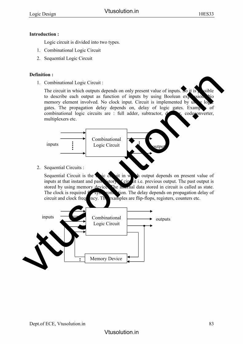
vtuso
lution
.in
Logic Design 10ES33
Dept.of ECE, Vtusolution.in 83
Introduction : Logic circuit is divided into two types.
1. Combinational Logic Circuit2. Sequential Logic Circuit
Definition : 1. Combinational Logic Circuit :
The circuit in which outputs depends on only present value of inputs. So it is possibleto describe each output as function of inputs by using Boolean expression. Nomemory element involved. No clock input. Circuit is implemented by using logicgates. The propagation delay depends on, delay of logic gates. Examples ofcombinational logic circuits are : full adder, subtractor, decoder, codeconverter,multiplexers etc.
2. Sequential Circuits :Sequential Circuit is the logic circuit in which output depends on present value ofinputs at that instant and past history of circuit i.e. previous output. The past output isstored by using memory device. The internal data stored in circuit is called as state.The clock is required for synchronization. The delay depends on propagation delay ofcircuit and clock frequency. The examples are flip-flops, registers, counters etc.
Combinational Logic Circuit inputs outputs
Combinational Logic Circuit
inputs outputs
Memory Device
Vtusolution.in
Vtusolution.in

vtuso
lution
.in
Logic Design 10ES33
Dept.of ECE, Vtusolution.in 84
Basic Bistable element.o Flip-Flop is Bistable element.o It consist of two cross coupled NOT Gates.o It has two stable states.
o Q and Q are two outputs complement of each other.o The data stored 1 or 0 in basic bistable element is state of flip-flop.o 1 – State is set condition for flip-flop.o 0 – State is reset / clear for flip-flop.o It stores 1 or 0 state as long power is ON.
Latches : S-R Latch : Set-reset Flip-Flop Latch is a storage device by using Flip-Flop. Latch can be controlled by direct inputs. Latch outputs can be controlled by clock or enable input.
Q and Q are present state for output.
Q+ and Q+ are next states for output. The function table / Truth table gives relation between inputs and outputs. The S=R=1 condition is not allowed in SR FF as output is unpredictable.
Vtusolution.in
Vtusolution.in
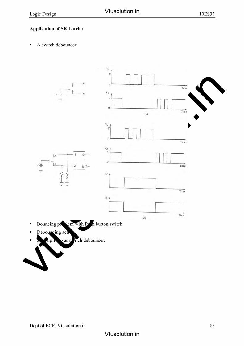
vtuso
lution
.in
Logic Design 10ES33
Dept.of ECE, Vtusolution.in 85
Application of SR Latch :
A switch debouncer
Bouncing problem with Push button switch. Debouncing action. SR Flip-Flop as switch debouncer.
Vtusolution.in
Vtusolution.in

vtuso
lution
.in
Logic Design 10ES33
Dept.of ECE, Vtusolution.in 86
Gated SR Latch :
Enable input C is clock input. C=1, Output changes as per input condition. C=0, No change of state. S=1, R=0 is set condition for Flip-flop. S=0, R=1 is reset condition for Flip-flop. S=R=1 is ambiguous state, not allowed.
Vtusolution.in
Vtusolution.in

vtuso
lution
.in
Logic Design 10ES33
Vtusolution.in
Vtusolution.in

vtuso
lution
.in
Logic Design 10ES33
Dept.of ECE, Vtusolution.in 88
Gated D Latch :
D Flip-Flop is Data Flip-Flop. D Flip-Flop stores 1 or 0. R input is complement of S. Only one D input is present. D Flip-Flop is a storage device used in register.
Vtusolution.in
Vtusolution.in
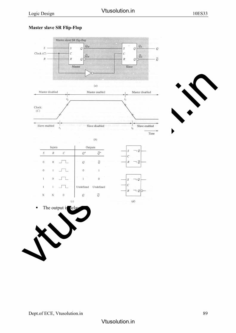
vtuso
lution
.in
Logic Design 10ES33
Dept.of ECE, Vtusolution.in 89
Master slave SR Flip-Flop
Two SR Flip-Flop, 1st is Master and 2nd is slave. Master Flip-Flop is positive edge triggered. Slave Flip-Flop is negative edge triggered. Slave follows master output. The output is delayed.
Vtusolution.in
Vtusolution.in
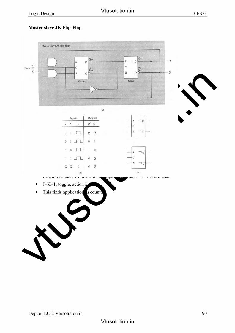
vtuso
lution
.in
Logic Design 10ES33
Dept.of ECE, Vtusolution.in 90
Master slave JK Flip-Flop
In SR Flip-Flop the input combination S=R=1 is not allowed. JK FF is modified version of SR FF. Due to feedback from slave FF output to master, J=K=1 is allowed. J=K=1, toggle, action in FF. This finds application in counter.
Vtusolution.in
Vtusolution.in

vtuso
lution
.in
Logic Design 10ES33
Dept.of ECE, Vtusolution.in 91
Positive Edge Triggered D Flip-Flop
When C=0, the output of AND Gate 2 & 3 is equal to 1.
If C=1, D=1, the output of AND Gate 2 is 0 and 3 is 1.
Recommended question and answer –unit-5 Jan 2009
Q.6 a) Design a 4-bit universal shift register using positive edge triggered D flip-flops tooperate as shown in the table .
S R 1, No Change of State
S R 1, Q =1 and Q 0 0,
Vtusolution.in
Vtusolution.in
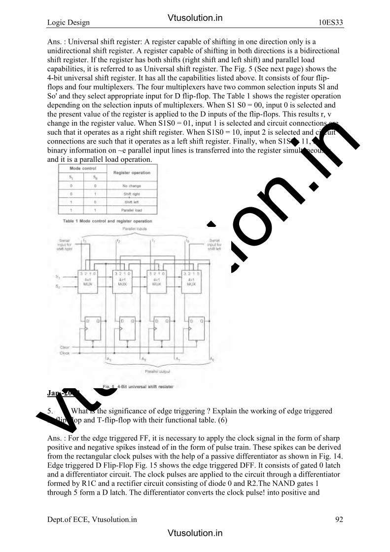
vtuso
lution
.in
Logic Design 10ES33
Dept.of ECE, Vtusolution.in 92
Ans. : Universal shift register: A register capable of shifting in one direction only is a unidirectional shift register. A register capable of shifting in both directions is a bidirectional shift register. If the register has both shifts (right shift and left shift) and parallel load capabilities, it is referred to as Universal shift register. The Fig. 5 (See next page) shows the 4-bit universal shift register. It has all the capabilities listed above. It consists of four flip-flops and four multiplexers. The four multiplexers have two common selection inputs Sl andSo' and they select appropriate input for D flip-flop. The Table 1 shows the register operationdepending on the selection inputs of multiplexers. When S1 S0 = 00, input 0 is selected andthe present value of the register is applied to the D inputs of the flip-flops. This results r, vchange in the register value. When S1S0 = 01, input 1 is selected and circuit connections aresuch that it operates as a right shift register. When S1S0 = 10, input 2 is selected and circuitconnections are such that it operates as a left shift register. Finally, when S1S0= 11, thebinary information on ~e parallel input lines is transferred into the register simultaneouslyand it is a parallel load operation.
Jan -2008
5. What is the significance of edge triggering ? Explain the working of edge triggeredD-flip-flop and T-flip-flop with their functional table. (6)
Ans. : For the edge triggered FF, it is necessary to apply the clock signal in the form of sharp positive and negative spikes instead of in the form of pulse train. These spikes can be derived from the rectangular clock pulses with the help of a passive differentiator as shown in Fig. 14. Edge triggered D Flip-Flop Fig. 15 shows the edge triggered DFF. It consists of gated 0 latch and a differentiator circuit. The clock pulses are applied to the circuit through a differentiator formed by R1C and a rectifier circuit consisting of diode 0 and R2.The NAND gates 1 through 5 form a D latch. The differentiator converts the clock pulse! into positive and
Vtusolution.in
Vtusolution.in

vtuso
lution
.in
Logic Design 10ES33
Dept.of ECE, Vtusolution.in 93
negative spikes as shown in the Fig. 16 and the combination of D and R2 will allow only the positive spikes to pass through blocking the negative spikes.
Vtusolution.in
Vtusolution.in

vtuso
lution
.in
Logic Design 10ES33
Dept.of ECE, Vtusolution.in 94
Aug 2009
i) Synchronous and asynchronous circuits.
ii) Combinational and sequential circuits.
b) Explain the working of 4-bit asynchronous counter.
1) 4 flip-flops are employed to create a 4-bit asynchronous counter as shown.2) The clock signal is connected to the clock input of only first stage flip-flop.3) Because of the inherent propagation delay time through a flip-flop, two
Vtusolution.in
Vtusolution.in

vtuso
lution
.in
Logic Design 10ES33
Dept.of ECE, Vtusolution.in 95
flip-flops never trigger simultaneously. Thus, it works in an asynchronous operation. 4) Output of the first flip-flop triggers the second flip-flop and so on.
S) At the output of flip-flops, we get the counted value of the counter.
1) Initially, the register is cleared.:. all the outputs QA' QSI QCI Qo are zero.2) The complement of Q 0 is 1 which is connected back to the D input of firststage.:. DA is, 1.:. The outPut becomes QA = 1, Qs = 0, Qc = a and Qo = O.3) The next clock pulse produces Q A = 1, Q B = 1, Q C = a and Q 0 = O.
The sequence is' given as :
Aug-2008
b) Fig. 2 shows a BCD counter that produces a 4-bit cutput representing
code for the number of pulses that have been applied to the counter i;
example, after four pulses have occurred, the counter ouq
(ABeD) = (OlOOh = (04)10' The counter resets to 0000 on the tenth]
starts counting over again. Design the logic circuit that produces a HIGl
Whenever the count is 2, 3 or 9. Use K - mapping and take advai
"don't care" conditions. Implement the logic circuit using NAND gates.
Vtusolution.in
Vtusolution.in

vtuso
lution
.in
Logic Design 10ES33
Dept.of ECE, Vtusolution.in 96
Vtusolution.in
Vtusolution.in

vtuso
lution
.in
Logic Design 10ES33
Dept.of ECE, Vtusolution.in 97
Aug -2008
Q.4 a) Design a 4 - bit BCD adder circuit using 7483 IC chip, with self correcting cirucit
i.e., .a provision has. to be made in the circuit, in case if the sum of the BCD
number exceeds 9. (12)
Vtusolution.in
Vtusolution.in

vtuso
lution
.in
Logic Design 10ES33
Dept.of ECE, Vtusolution.in 98
Aug-2007
Vtusolution.in
Vtusolution.in

vtuso
lution
.in
Logic Design 10ES33
Dept.of ECE, Vtusolution.in 99
Unit 6: 7 Hours
Sequential Circuits – 2: Characteristic Equations, Registers, Counters -Binary Ripple Counters, Synchronous Binary counters, Counters based on Shift Registers, Design of a Synchronous counters, Design of a Synchronous Mod-6 Counter using clocked JK Flip-Flops Design of a Synchronous Mod-6 Counter using clocked D, T, or SR Flip-Flops
Recommended readings:
1. Donald D Givone, “Digital Principles and Design “, Tata McGrawHill Edition, 2002.Unit - 6.6, 6.7, 6.8,6.9 – 6.9.1 and 6.9.2
Vtusolution.in
Vtusolution.in

vtuso
lution
.in
Logic Design 10ES33
Vtusolution.in
Vtusolution.in

vtuso
lution
.in
Logic Design 10ES33
Vtusolution.in
Vtusolution.in

vtuso
lution
.in
Logic Design 10ES33
Vtusolution.in
Vtusolution.in

vtuso
lution
.in
Logic Design 10ES33
Dept.of ECE, Vtusolution.in 103
COUNTERS
Counter is a register which counts the sequence in binary form. The state of counter changes with application of clock pulse. The counter is binary or non-binary. The total no. of states in counter is called as modulus. If counter is modulus-n, then it has n different states. State diagram of counter is a pictorial representation of counter states directed by
arrows in graph.
000
100
111
110
101
001
010
011
Fig. State diagram of mod-8 counter
Vtusolution.in
Vtusolution.in

vtuso
lution
.in
Logic Design 10ES33
104
Ripple and Arbitrary Counters In this lesson, you will learn about: _ Ripple Counters _ Counters with arbitrary count sequence Design of ripple Counters Two types of counters are identifiable: _ Synchronous counters, which have been discussed earlier, and _ Ripple counters. In ripple counters, flip-flop output transitions serve as a source for triggering other flipflops. In other words, clock inputs of the flip-flops are triggered by output transitions of other flip-flops, rather than a common clock signal. Typically, T flip-flops are used to build ripple counters since they are capable of complementing their content (See Figure 1). The signal with the pulses to be counted, i.e.“Pulse”, is connected to the clock input of the flip-flop that holds the LSB (FF # 1). The output of each FF is connected to the clock input of the next flip-flop in sequence. The flip-flops are negative edge triggered (bubbled clock inputs). T=1 for all FFs (J = K= 1). This means that each flip-flop complements its value if C input goes through a negative transition (1 _ 0).
Figure 1: A ripple counter
The previous ripple up-counter can be converted into a down-counter in one of two ways: _ Replace the negative-edge triggered FFs by positive-edge triggered FFs, or _ Instead of connecting C input of FF Qi to the output of the preceding FF (Qi-1) connect it to the complement output of that FF (Q/i-1).
Advantages of Ripple Counters: _ simple hardware and design.
Dept.of ECE, Vtusolution.in
Vtusolution.in
Vtusolution.in

vtuso
lution
.in
Logic Design 10ES33
Dept.of ECE, Vtusolution.in 105
Disadvantages of Ripple Counters: _ They are asynchronous circuits, and can be unreliable and delay dependent, if more logic is added. _ Large ripple counters are slow circuits due to the length of time required for the ripple to occur. Counters with Arbitrary Count Sequence: Design a counter that follows the count sequence: 0, 1, 2, 4, 5, 6. This counter can be designed with any flip-flop, but let‟s use the JK flip-flop. Notice that we have two “unused” states (3 and 7), which have to be dealt with (see Figure 2). These will be marked by don‟t cares in the state table (Refer to the design of sequential circuits with unused states discussed earlier). The state diagram of this counter is shown in Figure 2. In this figure, the unused states can go to any of the valid states, and the circuit can continue to count correctly. One possibility is to take state 7 (111) to 0 (000) and state 3 (011) to 4 (100).
Figure 2: State diagram for arbitrary counting sequence
The design approach is similar to that of synchronous circuits. The state transition table is built as shown in Figure 3 and the equations for all J and K inputs are derived. Notice that we have used don‟t care for the unused state (although we could have used 100 as the next state for 011, and 000 as the next state of 111).
Vtusolution.in
Vtusolution.in

vtuso
lution
.in
Logic Design 10ES33
Dept.of ECE, Vtusolution.in 106
Figure 3: State table for arbitrary counting sequence The computed J and K input equations are as follows: JA = B KA =B JB = C KB =1 JC = B/ KC =1
Figure 4: Circuit for arbitrary counting sequence
Vtusolution.in
Vtusolution.in

vtuso
lution
.in
Logic Design 10ES33
Vtusolution.in
Vtusolution.in

vtuso
lution
.in
Logic Design 10ES33
108
Counters In this lesson, the operation and design of Synchronous Binary Counters will be studied. Synchronous Binary Counters (SBC) Description and Operation In its simplest form, a synchronous binary counter (SBC) receives a train of clock pulses
as input and outputs the pulse count (Qn-1 …. Q2 Q1 Q0). An example is a 3-bit counter that counts from 000 upto 111. Each counter consists of a number of FFs. (Figure 1)
Figure 1: 3-bit SBC
In synchronous counters, all FFs are triggered by the same input clock. An n-bit counter has n-FFs with 2n distinct states, where each state corresponds to a particular count. Accordingly, the possible counts of an n-bit counter are 0 to (2n-1). Moreover an n-bit counter has n output bits (Qn-1 …. Q2 Q1 Q0). After reaching the maximum count of (2n-1), the following clock pulse resets the count back to 0. Thus, a 3-bit counter counts from 0 to 7 and back to 0. In other words, the output count actually equals (Total # of input pulses Modulo 2n). Accordingly, it is common to identify counters by the modulus 2n. For example, a 4-bit counter provides a modulo 16 count, a 3-bit counter is a modulo 8 counter, etc. Referring to the 3-bit counter mentioned earlier, each stage of the counter divides the frequency by 2, where the last stage divides the frequency by 2n, n being the number of bits. (Figure 2)
Dept.of ECE, Vtusolution.in
Vtusolution.in
Vtusolution.in

vtuso
lution
.in
Logic Design 10ES33
Dept.of ECE, Vtusolution.in 109
Figure 2: 3-bit SBC Thus, if the frequency (i.e. no. of cycles/ sec) of clock is F, then the frequency of output waveform of Q0 is F/2, Q1 is F/4, and so on. In general, for n-bit counter, we have F/2n. Design of Binary Counters (SBC) Design procedure is the same as for other synchronous circuits. A counter may operate without an external input (except for the clock pulses!) In this case, the output of the counter is taken from the outputs of the flip-flops without any additional outputs from gates. Thus, there are no columns for the input and outputs in the state table; we only see the current state and next state… Example Design a 4-bit SBC using JK flip-flops. The counter has 4 FFs with a total of 16 states, (0000 to 1111) _ 4 state variables Q3 Q2 Q1 Q0 are required.
Figure 3: State table for the example
Vtusolution.in
Vtusolution.in

vtuso
lution
.in
Logic Design 10ES33
Dept.of ECE, Vtusolution.in 110
Notice that the next state equals the present state plus one. To design this circuit, we derive the flip-flop input equations from the state transition table. Recall that to find J & K values, we have to use: _ The present state, _ The next state, and _ The JK flip-flop excitation table. When the count reaches 1111, it resets back to 0000, and the count cycle is repeated. Once the J and K values are obtained, the next step is to find out the simplified input equations by using K-maps, as shown in figure 4.
Figure 4: K-maps for the example
Notice that the maps for JQ0 and KQ0 are not drawn because the values in the table for these two variables either contain 1‟s or X‟s. This will result in JQ0 = KQ0 = 1 Note that the Boolean equation for J input is the same as that of the K input for all the FFs ⇒ Can use T-FFs instead of JK-FFs. Count Enable Control In many applications, controlling the counting operation is necessary ⇒ a count-enable (En) is required. If En= 1 then counting of incoming clock pulses is enabled Else if (En =0), no incoming clock pulse is counted. To accommodate the enable control, two approaches are possible. 1. Controlling the clock input of the counter2. Controlling FF excitation inputs (JK, T, D, etc.).Clock Control
Vtusolution.in
Vtusolution.in
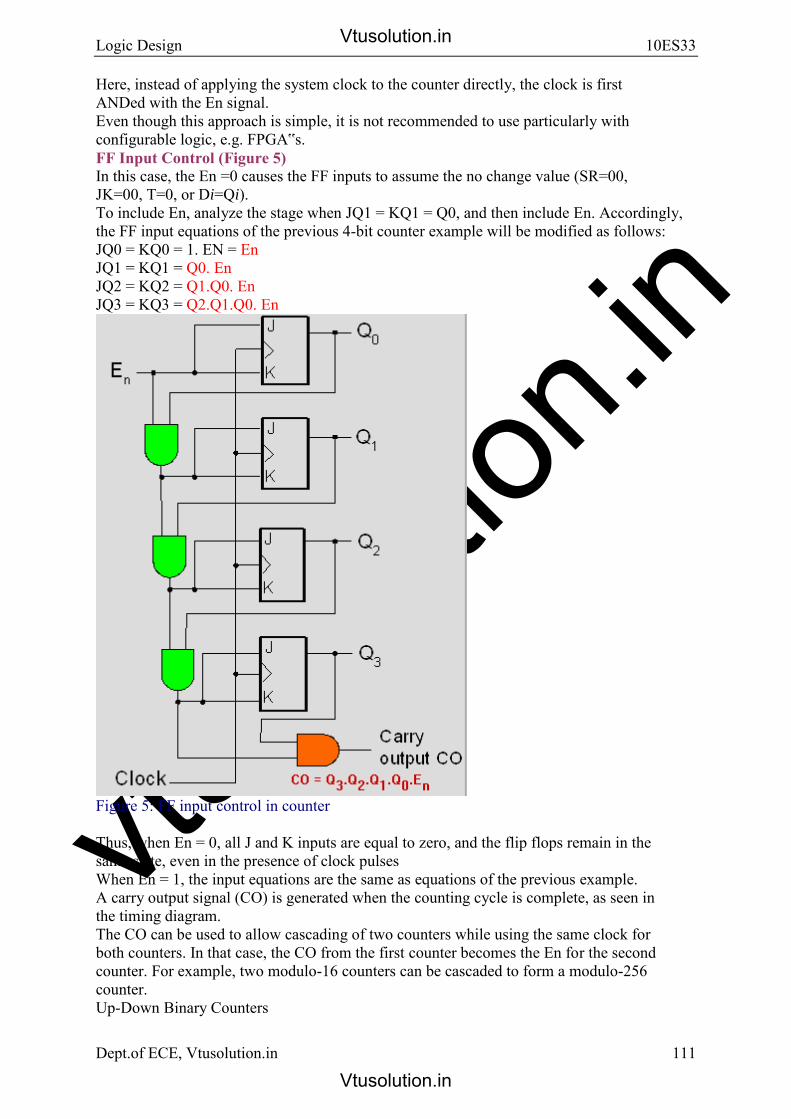
vtuso
lution
.in
Logic Design 10ES33
111
Here, instead of applying the system clock to the counter directly, the clock is first ANDed with the En signal. Even though this approach is simple, it is not recommended to use particularly with configurable logic, e.g. FPGA‟s. FF Input Control (Figure 5) In this case, the En =0 causes the FF inputs to assume the no change value (SR=00, JK=00, T=0, or Di=Qi). To include En, analyze the stage when JQ1 = KQ1 = Q0, and then include En. Accordingly, the FF input equations of the previous 4-bit counter example will be modified as follows: JQ0 = KQ0 = 1. EN = En JQ1 = KQ1 = Q0. En JQ2 = KQ2 = Q1.Q0. En JQ3 = KQ3 = Q2.Q1.Q0. En
Figure 5: FF input control in counter
Thus, when En = 0, all J and K inputs are equal to zero, and the flip flops remain in the same state, even in the presence of clock pulses When En = 1, the input equations are the same as equations of the previous example. A carry output signal (CO) is generated when the counting cycle is complete, as seen in the timing diagram. The CO can be used to allow cascading of two counters while using the same clock for both counters. In that case, the CO from the first counter becomes the En for the second counter. For example, two modulo-16 counters can be cascaded to form a modulo-256 counter. Up-Down Binary Counters
Dept.of ECE, Vtusolution.in
Vtusolution.in
Vtusolution.in

vtuso
lution
.in
Logic Design 10ES33
112
In addition to counting up, a SBC can be made to count down as well. A control input, S is required to control the direction of count. IF S= 1, the counter counts up, otherwise it counts down. FF Input Control Design a Modulo-8 up-down counter with control input S, such that if S= 1, the counter counts up, otherwise it counts down. Show how to provide a count enable input and a carry-out (CO) output. (See figures 6 & 7)
Figure 6: State diagram for FF input control example
Figure 7: State table for FF input control example The equations are (see figure 8) T0 = 1
Dept.of ECE, Vtusolution.in
Vtusolution.in
Vtusolution.in
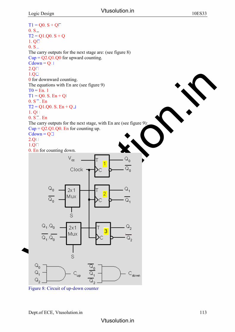
vtuso
lution
.in
Logic Design 10ES33
Dept.of ECE, Vtusolution.in 113
T1 = Q0. S + Q0. ST2 = Q1.Q0. S + Q1. Q0. SThe carry outputs for the next stage are: (see figure 8)Cup = Q2.Q1.Q0 for upward counting.Cdown = Q2.Q1.Q0 for downward counting.The equations with En are (see figure 9)T0 = En. 1T1 = Q0. S. En + Q0. S . EnT2 = Q1.Q0. S. En + Q1. Q0. S . EnThe carry outputs for the next stage, with En are (see figure 9):Cup = Q2.Q1.Q0. En for counting up.Cdown = Q2.Q1.Q0. En for counting down.
Figure 8: Circuit of up-down counter
Vtusolution.in
Vtusolution.in

vtuso
lution
.in
Logic Design 10ES33
Dept.of ECE, Vtusolution.in 114
Figure 9: Circuit of up-down counter with En
Vtusolution.in
Vtusolution.in

vtuso
lution
.in
Logic Design 10ES33
Vtusolution.in
Vtusolution.in

vtuso
lution
.in
Logic Design 10ES33
Vtusolution.in
Vtusolution.in

vtuso
lution
.in
Logic Design 10ES33
Vtusolution.in
Vtusolution.in

vtuso
lution
.in
Logic Design 10ES33
Vtusolution.in
Vtusolution.in

vtuso
lution
.in
Logic Design 10ES33
Dept.of ECE, Vtusolution.in 119
Jan-2008 i) Synchronous and asynchronous circuits.
ii) Combinational and sequential circuits.
b) Explain the working of 4-bit asynchronous counter.
Vtusolution.in
Vtusolution.in

vtuso
lution
.in
Logic Design 10ES33
Dept.of ECE, Vtusolution.in 120
1) 4 flip-flops are employed to create a 4-bit asynchronous counter as shown.2) The clock signal is connected to the clock input of only first stage flip-flop.3) Because of the inherent propagation delay time through a flip-flop, twoflip-flops never trigger simultaneously. Thus, it works in an asynchronousoperation.4) Output of the first flip-flop triggers the second flip-flop and so on.
S) At the output of flip-flops, we get the counted value of the counter.
1) Initially, the register is cleared.:. all the outputs QA' QSI QCI Qo are zero.2) The complement of Q 0 is 1 which is connected back to the D input of firststage.:. DA is, 1.:. The outPut becomes QA = 1, Qs = 0, Qc = a and Qo = O.3) The next clock pulse produces Q A = 1, Q B = 1, Q C = a and Q 0 = O.
The sequence is' given as :
Vtusolution.in
Vtusolution.in
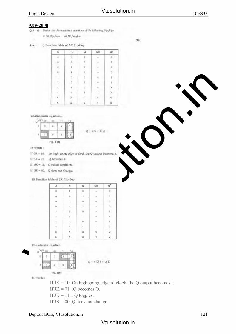
vtuso
lution
.in
Logic Design 10ES33
Dept.of ECE, Vtusolution.in 121
Aug-2008
If JK = 10, On high going edge of clock, the Q output becomes l. If JK = 01, .Q becomes O. If JK = 11, . Q toggles. If JK = 00, Q does not change.
Vtusolution.in
Vtusolution.in

vtuso
lution
.in
Logic Design 10ES33
Dept.of ECE, Vtusolution.in 122
b) Explain clearly the operation of an asynchronous inputs in a flip-flops with suitable
example. (6)Ans. : The best example of operation of asynchronous input to flip-flop is counter.Use of counter is to count the clock pulse. For these counters the external clocksignal is applied to one- flip-flop and then the output of preceding flip-flop is
connected to the clock of next flip-flop
Operation: 1) Initially both the flip-flops be in reset condition... QBQA = 002) On the first negative going clock edge : As the 1st falling edge of the clock hitsFF-A, it will toggle as TA = 1. Hence QA will be equal to 1. But for FF - B it has nochanged from 0 to I, it is treated as the positive clock edge by FF - B.
So
On second falling edge of clock pulse : On arrival of second falling cloCk edge, FF-A toggles again, to make QA = O. This change in QA (from 1 to 0) acts as a negative clock edge for FF-B. So it will also toggle, and QB will become 1.
Hence after the second clock pulse the counter output are
Both the outputs are changing their state. But both the changes do not take place simultaneously, QA will change first from 1 to 0 and then QB will change from 0 to 1. This is due to propagation delay of FF-A. So both flip-flops will never triggered at the
same instant. So it is asynchronous counter
Vtusolution.in
Vtusolution.in

vtuso
lution
.in
Logic Design 10ES33
Dept.of ECE, Vtusolution.in 123
c) An edge triggered 'D' flip-flop is connected as shown in the Fig. 10. Assume that AnQ = 0 initially and sketch the waveform and determine its frequency of the signal
at 'Q' output. (4)
Aug-2007
Vtusolution.in
Vtusolution.in
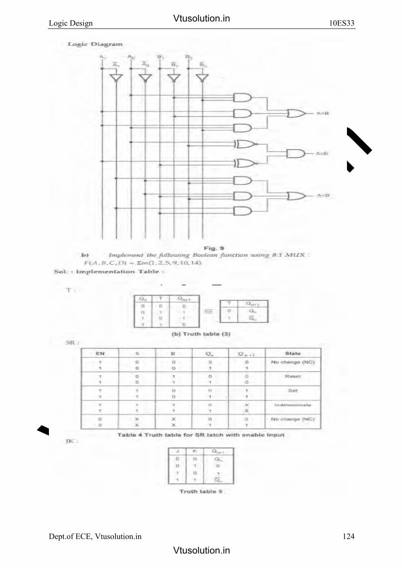
vtuso
lution
.in
Logic Design 10ES33
Dept.of ECE, Vtusolution.in 124
Vtusolution.in
Vtusolution.in
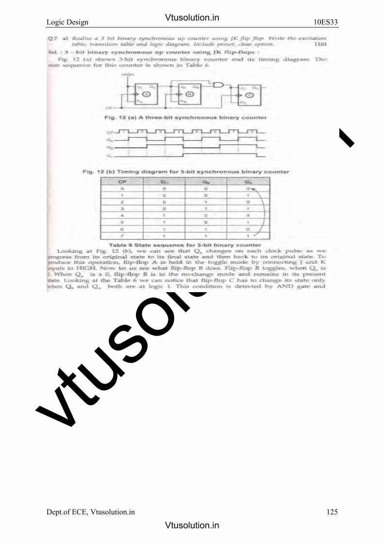
vtuso
lution
.in
Logic Design 10ES33
Dept.of ECE, Vtusolution.in 125
Vtusolution.in
Vtusolution.in

vtuso
lution
.in
Logic Design 10ES33
Dept.of ECE, Vtusolution.in 126
Unit 7: 6 Hours
Sequential Design - I: Introduction, Mealy and Moore Models, State Machine Notation, Synchronous Sequential Circuit Analysis
Recommended readings:
1. Donald D Givone, “Digital Principles and Design “, Tata McGrawHill Edition, 2002.
Units-6.1, 6.2, 6.3
Vtusolution.in
Vtusolution.in

vtuso
lution
.in
Logic Design 10ES33
Dept.of ECE, Vtusolution.in 127
Mealy and Moore Type Finite State Machines
Objectives
There are two basic ways to design clocked sequential circuits. These are using:
1. Mealy Machine, which we have seen so far.
2. Moore Machine.
The objectives of this lesson are:
1. Study Mealy and Moore machines
2. Comparison of the two machine types
3. Timing diagram and state machines
Mealy Machine
In a Mealy machine, the outputs are a function of the present state and the value of the inputs as shown in Figure 1.
Accordingly, the outputs may change asynchronously in response to any change in the inputs.
Figure 1: Mealy Type Machine
Vtusolution.in
Vtusolution.in

vtuso
lution
.in
Logic Design 10ES33
Dept.of ECE, Vtusolution.in 128
Mealy Machine
In a Moore machine the outputs depend only on the present state as shown in Figure 2.
A combinational logic block maps the inputs and the current state into the necessary flip-flop inputs to store the appropriate next state just like Mealy machine.
However, the outputs are computed by a combinational logic block whose inputs are only the flip-flops state outputs.
The outputs change synchronously with the state transition triggered by the active clock edge.
Figure 2: Moore Type Machine
Comparison of the Two Machine Types
Consider a finite state machine that checks for a pattern of „10‟ and asserts logic high when it is detected.
The state diagram representations for the Mealy and Moore machines are shown in Figure 3.
The state diagram of the Mealy machine lists the inputs with their associated outputs on state transitions arcs.
The value stated on the arrows for Mealy machine is of the form Zi/Xi where Zi represents input value and Xi represents output value.
A Moore machine produces a unique output for every state irrespective of inputs.
�
state in the form state-notation/output-value.
Vtusolution.in
Vtusolution.in

vtuso
lution
.in
Logic Design 10ES33
Dept.of ECE, Vtusolution.in 129
� arrows of Moore machine are labeled with the input value that triggers such transition.
�
generated in fewer states using Mealy machine as compared to Moore machine. This was illustrated in the previous example.
Figure 3: Mealy and Moore State Diagrams for '10' Sequence Detector
Timing Diagrams
�
state-machine outputs „1‟ if the input is „1‟ for three consecutive clocks.
Vtusolution.in
Vtusolution.in

vtuso
lution
.in
Logic Design 10ES33
Dept.of ECE, Vtusolution.in 130
Figure 4: Mealy State Machine for '111' Sequence Detector
Mealy State Machine
� The Mealy machine state diagram is shown in Figure 4.
� Note that there is no reset condition in the state machine that employs two flip-flops. This means that the state machine can enter its unused state „11‟ on start up.
� To make sure that machine gets resetted to a valid state, we use a „Reset‟ signal.
� The logic diagram for this state machine is shown in Figure 5. Note that negative edge triggered flip-flops are used.
Figure 5: Mealy State Machine Circuit Implementation
� Since the output in Mealy model is a combination of present state and input values, an unsynchronized input with triggering clock may result in invalid output, as in the present case.
Vtusolution.in
Vtusolution.in

vtuso
lution
.in
Logic Design 10ES33
Dept.of ECE, Vtusolution.in 131
� Consider the present case where input „x‟ remains high for sometime after state „AB = 10‟ is reached. This results in „False Output‟, also known as „Output Glitch‟.
Figure 6: Timing Diagram for Mealy Model Sequence Detector
Moore State Machine
� The Moore machine state diagram for „111‟ sequence detector is shown in Figure 7.
� The state diagram is converted into its equivalent state table (See Table 1).
� The states are next encoded with binary values and we achieve a state transition table (See Table 2).
Figure 7: Moore Machine State Diagram
Vtusolution.in
Vtusolution.in

vtuso
lution
.in
Logic Design 10ES33
Dept.of ECE, Vtusolution.in 132
� We will use JK and D flip-flops for the Moore circuit implementation. The excitation tables for JK and D flip-flops (Table 3 & 4) are referenced to tabulate excitation table (See Table 5).
� Simplifying Table 5 using maps, we get the following equations:
Vtusolution.in
Vtusolution.in
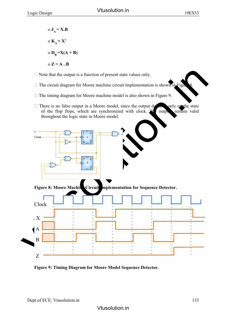
vtuso
lution
.in
Logic Design 10ES33
Dept.of ECE, Vtusolution.in 133
o JA = X.B
o KA = X’
o DB =X(A + B)
o Z = A . B
� Note that the output is a function of present state values only.
� The circuit diagram for Moore machine circuit implementation is shown in Figure 8.
� The timing diagram for Moore machine model is also shown in Figure 9.
� There is no false output in a Moore model, since the output depends only on the state of the flop flops, which are synchronized with clock. The outputs remain valid throughout the logic state in Moore model.
Figure 8: Moore Machine Circuit Implementation for Sequence Detector.
Figure 9: Timing Diagram for Moore Model Sequence Detector.
Vtusolution.in
Vtusolution.in

vtuso
lution
.in
Logic Design 10ES33
Dept.of ECE, Vtusolution.in 134
Recommended question and answer –unit-7 Jan -2009 Q.7 b) Give output function, excitation table and state transition diagram by analyzing the
sequential circuit shown in Fig. 7.(12)
Vtusolution.in
Vtusolution.in
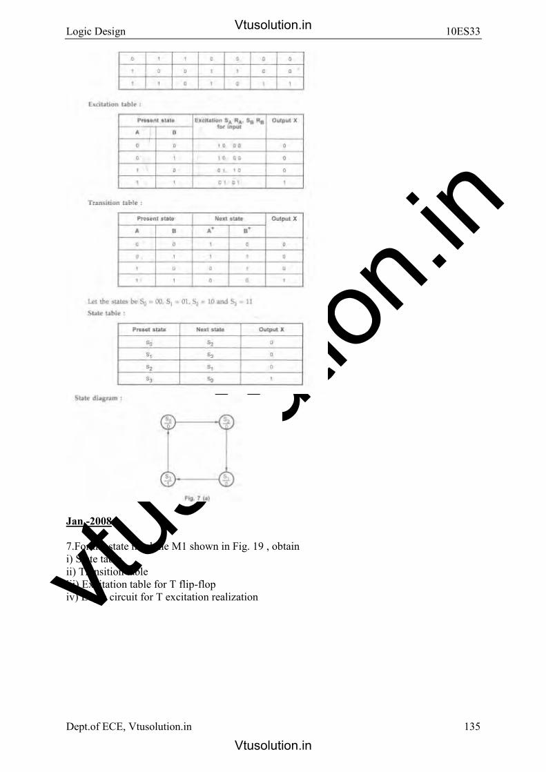
vtuso
lution
.in
Logic Design 10ES33
Dept.of ECE, Vtusolution.in 135
Jan -2008
7.For the state machine M1 shown in Fig. 19 , obtaini) State tableii) Transition tableiii) Excitation table for T flip-flopiv) Logic circuit for T excitation realization
Vtusolution.in
Vtusolution.in

vtuso
lution
.in
Logic Design 10ES33
Dept.of ECE, Vtusolution.in 136
Vtusolution.in
Vtusolution.in

vtuso
lution
.in
Logic Design 10ES33
137
Aug-2009
c.State the rules for state assignments.
Ans. : Rules for state assignmentsThere are two basic rules for making state assignments.
Dept.of ECE, Vtusolution.in
Vtusolution.in
Vtusolution.in

vtuso
lution
.in
Logic Design 10ES33
Dept.of ECE, Vtusolution.in 138
Rule 1: States having the same NEXT STATES for a given input condition should have assignments which can be grouped into logically adjacent cells in a K-map. Fig. 12 shows the' example for Rule 1. As shown in the Fig. 12, there are four states whose next state is same. Thus states assignments for these states are 100,
101,110 and 111, which can be grouped into logically adjacent cells in a K-map.
Rule 2: States that are the NEXT STATES of a single state should have assignment which can be grouped into logically adjacent cells in a K-map. Fig. 13 shows the example for Rule 2. As shown in the Fig. 13 for state 000, there
are four next states. These states are assigned as 100, 101, 110 and 111 so that they can
be grouped into logically adjacent cells in a K-map and table shows the state table with assigned statt
Aug 2008
7. b) Construct the state table for the following state diagram.
Vtusolution.in
Vtusolution.in

vtuso
lution
.in
Logic Design 10ES33
139
Aug-2007 applied to the J and K inputs of flip-flop C. Whenever both QA and QB are HIGH, the output of the AND gate makes the J and K inputs of flip-flop C HIGH, and flip-flop C toggles on the following clock pulse. At all other times, the J and K inputs of flip-flop C are held LOW by the AND gate qutput, and flip-flop does not change state. b) Explain the different types of shift register. 5150, SIPO, PIPO, PISO with relevant
circuit diagram. . [10]Sol. :SISO Shift Register:
Fig. 13 shows serial in serial out shift-left register. We will illustrate the entry of the four bit biIlary number 1111 into the register, beginning with the left-most bit. Initially, register is cleared. SO QAQBQCQO = 0000 a) When data 1 1 1 1 is applied serially, Le.left-most 1 is applied as Din'Din = 1, QAQBQCQo = 00 0 0The arrival of the first falling clock edge sets the right-most flip-flop, and thestored word becomes, .QAQBQCQO = 000 1b) When the next negative clock edge hits, the Q1 flip-flop sets and the registercontents become,QAQBQCQO = 001 1c) The third negative clock edge results in,QAQBQCQO = b 1 1 1d) The fourth falling clock edge gives,QAQBQCQo = 1 1 1 1SIPO Shift Register: In this case, the data bits are entered into the register in thesame manner as discussed in the last section, i.e. serially. But the output is taken inparallel. Once the data are stored, each bit appears on its respective output line andall bits are available simultaneously, instead of on a bit-by-bit basis as with the serialoutput as shown in Fig. 14.
PIPO Shift Register : From the third and second types of registers, it is cleared that how to enter the data LT\ parallel i.e. all bits simultaneously into the register and how to take data out in parallel from the register. In 'parallel in parallel out register',
Dept.of ECE, Vtusolution.in
Vtusolution.in
Vtusolution.in
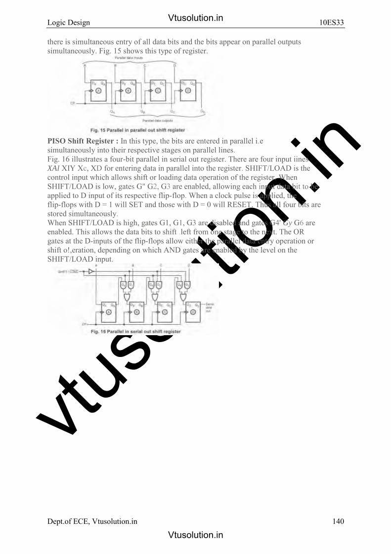
vtuso
lution
.in
Logic Design 10ES33
Dept.of ECE, Vtusolution.in 140
there is simultaneous entry of all data bits and the bits appear on parallel outputs simultaneously. Fig. 15 shows this type of register.
PISO Shift Register : In this type, the bits are entered in parallel i.e simultaneously into their respective stages on parallel lines. Fig. 16 illustrates a four-bit parallel in serial out register. There are four input iines XAI XIY Xc, XD for entering data in parallel into the register. SHIFT/LOAD is the control input which allows shift or loading data operation of the register. When SHIFT/LOAD is low, gates G" G2, G3 are enabled, allowing each input data bit to be applied to D input of its respective flip-flop. When a clock pulse is applied, the flip-flops with D = 1 will SET and those with D = 0 will RESET. Thus all four bits are stored simultaneously. When SHIFT/LOAD is high, gates G1, G1, G3 are disabled and gates G4' Gy G6 are enabled. This allows the data bits to shift .left from one stage to the next. The OR gates at the D-inputs of the flip-flops allow either the parallel data entry operation or shift o!,eration, depending on which AND gates are enabled by the level on the SHIFT/LOAD input.
Vtusolution.in
Vtusolution.in

vtuso
lution
.in
Logic Design 10ES33
Dept.of ECE, Vtusolution.in 141
Unit 8: 6 Hours
Sequential Design - II: Construction of state Diagrams, Counter Design
Recommended readings:
1. Donald D Givone, “Digital Principles and Design “, Tata McGrawHill Edition, 2002.
Units- 6.4, 6.5
Vtusolution.in
Vtusolution.in

vtuso
lution
.in
Logic Design 10ES33
Dept.of ECE, Vtusolution.in 142
Design of Synchronous Sequential Circuits Objectives
1. Design of synchronous sequential circuits with an example.
2. Construction of state diagrams and state tables/
3. Translation of State transition table into excitation table.
4. Logic diagram construction of a synchronous sequential circuit
Sequential Circuit Design Steps
� ations of the problem (See Figure 1).
Figure 1: Sequential Circuit Design Steps
The next step is to derive the state table of the sequential circuit. A state table represents the verbal specifications in a tabular form.
In certain cases state table can be derived directly from verbal description of the problem.
In other cases, it is easier to first obtain a state diagram from the verbal description and then obtain the state table from the state diagram.
A state diagram is a graphical representation of the sequential circuit.
In the next step, we proceed by simplifying the state table by minimizing the number of states and obtain a reduced state table.
Vtusolution.in
Vtusolution.in

vtuso
lution
.in
Logic Design 10ES33
Dept.of ECE, Vtusolution.in 143
The states in the reduced state table are then assigned binary-codes. The resulting table is called output and state transition table.
From the state transition table and using flip-flop‟s excitation tables, flip-flops input equations are derived. Furthermore, the output equations can readily be derived as well.
Finally, the logic diagram of the sequential circuit is constructed.
An example will be used to illustrate all these concepts.
Sequence Recognizer
A sequence recognizer is to be designed to detect an input sequence of „1011‟. The sequence recognizer outputs a „1‟ on the detection of this input sequence. The sequential circuit is to be designed using JK and D type flip-flops.
A sample input/output trace for the sequence detector is shown in Table 1.
Table 1: Sample Input/Output Trace
We will begin solving the problem by first forming a state diagram from the verbal description.
A state diagram consists of circles (which represent the states) and directed arcs that connect the circles and represent the transitions between states.
In a state diagram:
1. The number of circles is equal to the number of states. Every state is given alabel (or a binary encoding) written inside the corresponding circle.
2. The number of arcs leaving any circle is 2n
, where n is the number of inputs of the sequential circuit.
3. The label of each arc has the notation x/y, where x is the input vector thatcauses the state transition, and y is the value of the output during that presentstate.
4. An arc may leave a state and end up in the same or any other state.
Vtusolution.in
Vtusolution.in

vtuso
lution
.in
Logic Design 10ES33
Dept.of ECE, Vtusolution.in 144
Before we begin our design, the following should be noted 1. We do not have an idea about how many states the machine will have.
2. The states are used to “remember” something about the history of past inputs.For the sequence 1011, in order to be able to produce the output value 1 whenthe final 1 in the sequence is received, the circuit must be in a state that “remembers” that the previous three inputs were 101.
3. There can be more than one possible state machine with the same behavior.
. Deriving the State Diagram
Let us begin with an initial state (since a state machine must have at least one state) and denote it with ‘S0’ as shown in Figure 2 (a).
Two arcs leave state ‘S0’ depending on the input (being a 0 or a 1). If the input is a 0, then we return back to the same state. If the input is a 1, then we have to remember it (recall that we are trying to detect a sequence of 1011). We remember that the last input was a one by changing the state of the machine to a new state, say ‘S1’. This is illustrated in Figure 2 (b).
‘S1’ represents a state when the last single bit of the sequence was one. Outputs for both transitions are zero, since we have not detected what we are looking for.
Again in state ‘S1’, we have two outgoing arcs. If the input is a 1, then we return to the same state and if the input is a 0, then we have to remember it (second number in the sequence). We can do so by transiting to a new state, say ‘S2’. This is illustrated in Figure 2 (c).
Note that if the input applied is „1‟, the next state is still ‘S1’ and not the initial state ‘S0’. This is because we take this input 1 as the first digit of new sequence. The output still remains 0 as we have not detected the sequence yet.
State ‘S2’ represents detection of „10‟ as the last two bits of the sequence. If now the input is a „1‟, we have detected the third bit in our sequence and need to remember it. We remember it by transiting to a new state, say ‘S3’ as shown in Figure 2 (d). If the input is „0‟ in state ‘S2’ then it breaks the sequence and we need to start all over again. This is achieved by transiting to initial state ‘S0’. The outputs are still 0.
In state ‘S3’, we have detected input sequence „101‟. Another input 1 completes our detection sequence as shown in Figure 2 (e). This is signaled by an output 1. However we transit to state ‘S1’ instead of ‘S0’ since this input 1 can be counted as first 1 of a new sequence. Application of input 0 to state ‘S3’ means an input sequence of 1010. This implies the last two bits in the sequence were 10 and we transit to a state that remembers this input sequence, i.e. state ‘S2’. Output remains as zero.
Vtusolution.in
Vtusolution.in

vtuso
lution
.in
Logic Design 10ES33
Dept.of ECE, Vtusolution.in 145
Figure 2: Deriving the State Diagram of the Sequence Recognizer
Deriving the State Table
A state table represents time sequence of inputs, outputs, and states in a tabular form. The state table for the previous state diagram is shown in Table 2.
The state table can also be represented in an alternate form as shown in Table 3.
Here the present state and inputs are tabulated as inputs to the combinational circuit. For every combination of present state and input, next state column is filled from the state table.
The number of flip-flops required is equal to [log2(number of states)]. Thus, the state machine given in the figure will require two flip- 2
assign letters A and B to them.
Vtusolution.in
Vtusolution.in

vtuso
lution
.in
Logic Design 10ES33
Dept.of ECE, Vtusolution.in 146
State Assignment
The states in the constructed state diagram have been assigned symbolic names rather than binary codes.
It is necessary to replace these symbolic names with binary codes in order to proceed with the design.
In general, if there are m states, then the codes must contain n bits, where 2n
≥ m, and each state must be assigned a unique code.
There can be many possible assignments for our state machine. One possible assignment is show in Table 4.
Table 4: State Assignment
� The assignment of state codes to states results in state transition table as shown.
� It is important to mention here that the binary code of the present state at a given time t represents the values stored in the flip-flops; and the next-state represents the values of the flip-flops one clock period later, at time t+1.
Vtusolution.in
Vtusolution.in

vtuso
lution
.in
Logic Design 10ES33
Dept.of ECE, Vtusolution.in 147
General Structure of Sequence Recognizer
� The specifications required using JK and D type flip-flops.
Referring to the general structure of sequential circuit shown in Figure 3, our synthesized circuit will look like that as shown in the figure. Observe the feedback paths.
Figure 3: General Structure of the Sequenc Recognizer
� What remains to be determined is the combinational circuit which specifies the external outputs and the flip-flop inputs.
� The state transition table as shown can now be expanded to construct the excitation table for the circuit.
� Since we are designing the sequential circuit using JK and D type flip-flops, we need to correlate the required transitions in state transition table with the excitation tables of JK and D type-flip-flops.
� The functionality of the required combinational logic is encapsulated in the excitation table. Thus, the excitation table is next simplified using map or other simplification methods to yield Boolean expressions for inputs of the used flip-flops as well as the circuit outputs.
Deriving the Excitation Table
Vtusolution.in
Vtusolution.in

vtuso
lution
.in
Logic Design 10ES33
Dept.of ECE, Vtusolution.in 148
� The excitation table (See Table 6) describes the behavior of the combinational portion of sequential circuit.
Table 6: Excitation Table of the Sequence Recognizer
� For deriving the actual circuitry for the combinational circuit, we need to simplify the excitation table in a similar way we used to simplify truth tables for purely combinational circuits.
� Whereas in combinational circuits, our concern were only circuit outputs; in sequential circuits, the combinational circuitry is also feeding the flip-flops inputs. Thus, we need to simplify the excitation table for both outputs as well as flip-flops inputs.
� We can simplify flip-flop inputs and output using K-maps as shown in Figure 4.
� Finally the logic diagram of the sequential circuit can be made as shown in Figure 5.
Figure 4: Input Equations of the Sequence Recognizer
Vtusolution.in
Vtusolution.in

vtuso
lution
.in
Logic Design 10ES33
Dept.of ECE, Vtusolution.in 149
Figure 5: Circuit Diagram of the Sequence Recognizer
Recommended question and answer –unit-8 Q.8 a) Design a cyclic mod-6 synchronous binary counter ? state diagram, transition table
using JK flip-flop. (10)Ans. : Design of a synchronous mod-6 counter using clocked JK flip-flops The counter with nflip-flops has maximum mod number 2". For example, 3-bit binary counter is a mod 8counter. This basic counter can be modified to produce MOD numbers less than 2" byallowing the counter to skip states those are normallypart of counting sequence. Let us design mod-6 counter using clocked JK flip-flops.Step 1 : Find number of flip-flops required to build the counter : Flip-Flops required are: 2n>= N.Here N = 6 :. n = 3i.e. three flip-flops are required.Step 2 : Write an excitation table for JK flip-flop.
Vtusolution.in
Vtusolution.in

vtuso
lution
.in
Logic Design 10ES33
Dept.of ECE, Vtusolution.in 150
Vtusolution.in
Vtusolution.in

vtuso
lution
.in
Logic Design 10ES33
Dept.of ECE, Vtusolution.in 151
Jan-2008
Q.8 a) Construct a mealy state diagram that will detect a serial sequence of 10110.WIrthe input pattern has been detected, cause an output Z to be asserted high. I
Vtusolution.in
Vtusolution.in
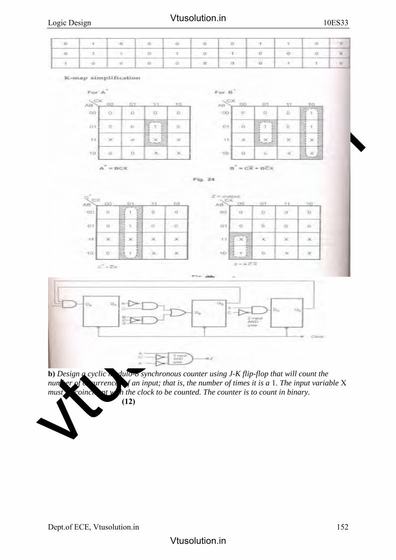
vtuso
lution
.in
Logic Design 10ES33
Dept.of ECE, Vtusolution.in 152
b) Design a cyclic modulo-8 synchronous counter using J-K flip-flop that will count the
number of occurrences of an input; that is, the number of times it is a 1. The input variable Xmust be coincident with the clock to be counted. The counter is to count in binary.
(12)
Vtusolution.in
Vtusolution.in

vtuso
lution
.in
Logic Design 10ES33
Dept.of ECE, Vtusolution.in 153
Aug 2009
c.State the rules for state assignments.
Ans. : Rules for state assignmentsThere are two basic rules for making state assignments.Rule 1: States having the same NEXT STATES for a given input condition shouldhave assignments which can be grouped into logically adjacent cells in a K-map.Fig. 12 shows the' example for Rule 1. As shown in the Fig. 12, there are fourstates whose next state is same. Thus states assignments for these states are 100,
101,110 and 111, which can be grouped into logically adjacent cells in a K-map.
Vtusolution.in
Vtusolution.in

vtuso
lution
.in
Logic Design 10ES33
Dept.of ECE, Vtusolution.in 154
Rule 2: States that are the NEXT STATES of a single state should have assignment which can be grouped into logically adjacent cells in a K-map. Fig. 13 shows the example for Rule 2. As shown in the Fig. 13 for state 000, there
are four next states. These states are assigned as 100, 101, 110 and 111 so that they can
be grouped into logically adjacent cells in a K-map and table shows the state table with assigned statt
Aug-2008
Q.8 a) Design a· clocked sequential circuit that operates according to the state diagram
shown. Implement the circuit using D flip-flop. (12)
Vtusolution.in
Vtusolution.in

vtuso
lution
.in
Logic Design 10ES33
Dept.of ECE, Vtusolution.in 155
b) Design a counter using JK flip-flops whose counting sequence is 000, 001, 100,
110, 111, 101, 000 etc. by obtaining its minimal sum equations. (8)
Vtusolution.in
Vtusolution.in

vtuso
lution
.in
Logic Design 10ES33
Dept.of ECE, Vtusolution.in 156
Vtusolution.in
Vtusolution.in

vtuso
lution
.in
Logic Design 10ES33
Dept.of ECE, Vtusolution.in 157
Aug-2007
Vtusolution.in
Vtusolution.in
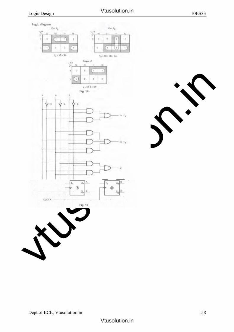
vtuso
lution
.in
Logic Design 10ES33
Dept.of ECE, Vtusolution.in 158
Vtusolution.in
Vtusolution.in