virtex-6 fpga system monitor - all programmable · virtex-6 fpga system monitor ug370 (v1.2)...
TRANSCRIPT
Virtex-6 FPGA System Monitor
User Guide
UG370 (v1.2) September 18, 2014
Virtex-6 FPGA System Monitor www.xilinx.com UG370 (v1.2) September 18, 2014
Notice of DisclaimerThe information disclosed to you hereunder (the “Materials”) is provided solely for the selection and use of Xilinx products. To the maximum extent permitted by applicable law: (1) Materials are made available "AS IS" and with all faults, Xilinx hereby DISCLAIMS ALL WARRANTIES AND CONDITIONS, EXPRESS, IMPLIED, OR STATUTORY, INCLUDING BUT NOT LIMITED TO WARRANTIES OF MERCHANTABILITY, NON-INFRINGEMENT, OR FITNESS FOR ANY PARTICULAR PURPOSE; and (2) Xilinx shall not be liable (whether in contract or tort, including negligence, or under any other theory of liability) for any loss or damage of any kind or nature related to, arising under, or in connection with, the Materials (including your use of the Materials), including for any direct, indirect, special, incidental, or consequential loss or damage (including loss of data, profits, goodwill, or any type of loss or damage suffered as a result of any action brought by a third party) even if such damage or loss was reasonably foreseeable or Xilinx had been advised of the possibility of the same. Xilinx assumes no obligation to correct any errors contained in the Materials or to notify you of updates to the Materials or to product specifications. You may not reproduce, modify, distribute, or publicly display the Materials without prior written consent. Certain products are subject to the terms and conditions of Xilinx’s limited warranty, please refer to Xilinx’s Terms of Sale which can be viewed at www.xilinx.com/legal.htm#tos; IP cores may be subject to warranty and support terms contained in a license issued to you by Xilinx. Xilinx products are not designed or intended to be fail-safe or for use in any application requiring fail-safe performance; you assume sole risk and liability for use of Xilinx products in such critical applications, please refer to Xilinx’s Terms of Sale which can be viewed at www.xilinx.com/legal.htm#tos.
Automotive Applications DisclaimerXILINX PRODUCTS ARE NOT DESIGNED OR INTENDED TO BE FAIL-SAFE, OR FOR USE IN ANY APPLICATION REQUIRING FAIL-SAFE PERFORMANCE, SUCH AS APPLICATIONS RELATED TO: (I) THE DEPLOYMENT OF AIRBAGS, (II) CONTROL OF A VEHICLE, UNLESS THERE IS A FAIL-SAFE OR REDUNDANCY FEATURE (WHICH DOES NOT INCLUDE USE OF SOFTWARE IN THE XILINX DEVICE TO IMPLEMENT THE REDUNDANCY) AND A WARNING SIGNAL UPON FAILURE TO THE OPERATOR, OR (III) USES THAT COULD LEAD TO DEATH OR PERSONAL INJURY. CUSTOMER ASSUMES THE SOLE RISK AND LIABILITY OF ANY USE OF XILINX PRODUCTS IN SUCH APPLICATIONS.
© Copyright 2009—2014 Xilinx, Inc. Xilinx, the Xilinx logo, Artix, ISE, Kintex, Spartan, Virtex, Vivado, Zynq, and other designated brands included herein are trademarks of Xilinx in the United States and other countries. All other trademarks are the property of their respective owners.
Revision HistoryThe following table shows the revision history for this document.
Version Revision
06/24/2009 1.0 Initial Xilinx release.
06/14/2010 1.1 Updated VREFP values in Table 7, Table 13,and Table 15. In Figure 24, replaced MAX6120 with MAX6018.
09/18/2014 1.2 Updated Additional Support Resources and Thermal Management. Added a note to Table 9.
Virtex-6 FPGA System Monitor www.xilinx.com 3UG370 (v1.2) September 18, 2014
Revision History . . . . . . . . . . . . . . . . . . . . . . . . . . . . . . . . . . . . . . . . . . . . . . . . . . . . . . . . . . . . . 2
Preface: About This GuideAdditional Documentation . . . . . . . . . . . . . . . . . . . . . . . . . . . . . . . . . . . . . . . . . . . . . . . . . . . 5Additional Support Resources . . . . . . . . . . . . . . . . . . . . . . . . . . . . . . . . . . . . . . . . . . . . . . . . 6
Virtex-6 FPGA System MonitorSystem Monitor Primitive . . . . . . . . . . . . . . . . . . . . . . . . . . . . . . . . . . . . . . . . . . . . . . . . . . . . 8
System Monitor Ports . . . . . . . . . . . . . . . . . . . . . . . . . . . . . . . . . . . . . . . . . . . . . . . . . . . . . . 8User Attributes . . . . . . . . . . . . . . . . . . . . . . . . . . . . . . . . . . . . . . . . . . . . . . . . . . . . . . . . . . . 10
Pre-Configuration Operation . . . . . . . . . . . . . . . . . . . . . . . . . . . . . . . . . . . . . . . . . . . . . . . . 10Analog-to-Digital Converter . . . . . . . . . . . . . . . . . . . . . . . . . . . . . . . . . . . . . . . . . . . . . . . . . 11
Temperature Sensor . . . . . . . . . . . . . . . . . . . . . . . . . . . . . . . . . . . . . . . . . . . . . . . . . . . . . . . 12Power Supply Sensor . . . . . . . . . . . . . . . . . . . . . . . . . . . . . . . . . . . . . . . . . . . . . . . . . . . . . . 14
Register File Interface . . . . . . . . . . . . . . . . . . . . . . . . . . . . . . . . . . . . . . . . . . . . . . . . . . . . . . . 14Status Registers. . . . . . . . . . . . . . . . . . . . . . . . . . . . . . . . . . . . . . . . . . . . . . . . . . . . . . . . . . . 15
Flag Register . . . . . . . . . . . . . . . . . . . . . . . . . . . . . . . . . . . . . . . . . . . . . . . . . . . . . . . . . . 17Control Registers . . . . . . . . . . . . . . . . . . . . . . . . . . . . . . . . . . . . . . . . . . . . . . . . . . . . . . . . . 17
Configuration Registers (40h to 42h) . . . . . . . . . . . . . . . . . . . . . . . . . . . . . . . . . . . . . . . 17Test Registers (43h to 47h). . . . . . . . . . . . . . . . . . . . . . . . . . . . . . . . . . . . . . . . . . . . . . . 21Channel Sequencer Registers (48h to 4Fh). . . . . . . . . . . . . . . . . . . . . . . . . . . . . . . . . . . 21Alarm Registers (50h to 57h) . . . . . . . . . . . . . . . . . . . . . . . . . . . . . . . . . . . . . . . . . . . . . 21
DRP JTAG Interface . . . . . . . . . . . . . . . . . . . . . . . . . . . . . . . . . . . . . . . . . . . . . . . . . . . . . . . 21System Monitor DRP JTAG Write Operation . . . . . . . . . . . . . . . . . . . . . . . . . . . . . . . . . 21System Monitor JTAG DRP Read Operation . . . . . . . . . . . . . . . . . . . . . . . . . . . . . . . . . 22JTAG DRP Commands . . . . . . . . . . . . . . . . . . . . . . . . . . . . . . . . . . . . . . . . . . . . . . . . . . 23DRP Arbitration . . . . . . . . . . . . . . . . . . . . . . . . . . . . . . . . . . . . . . . . . . . . . . . . . . . . . . . 24JTAGBUSY . . . . . . . . . . . . . . . . . . . . . . . . . . . . . . . . . . . . . . . . . . . . . . . . . . . . . . . . . . . 24JTAGMODIFIED. . . . . . . . . . . . . . . . . . . . . . . . . . . . . . . . . . . . . . . . . . . . . . . . . . . . . . . 24JTAGLOCKED . . . . . . . . . . . . . . . . . . . . . . . . . . . . . . . . . . . . . . . . . . . . . . . . . . . . . . . . 24
System Monitor Control Logic. . . . . . . . . . . . . . . . . . . . . . . . . . . . . . . . . . . . . . . . . . . . . . . 25Channel Sequencer . . . . . . . . . . . . . . . . . . . . . . . . . . . . . . . . . . . . . . . . . . . . . . . . . . . . . . . 25
ADC Channel Selection (48h and 49h) . . . . . . . . . . . . . . . . . . . . . . . . . . . . . . . . . . . . . 26ADC Channel Averaging (4Ah and 4Bh) . . . . . . . . . . . . . . . . . . . . . . . . . . . . . . . . . . . . 27ADC Channel Analog-Input Mode (4Ch and 4Dh). . . . . . . . . . . . . . . . . . . . . . . . . . . . . 29ADC Channel Acquisition Time (4Eh and 4Fh) . . . . . . . . . . . . . . . . . . . . . . . . . . . . . . . 29
Maximum and Minimum Status Registers . . . . . . . . . . . . . . . . . . . . . . . . . . . . . . . . . . . 29Automatic Alarms . . . . . . . . . . . . . . . . . . . . . . . . . . . . . . . . . . . . . . . . . . . . . . . . . . . . . . . . 29
Supply Sensor Alarms . . . . . . . . . . . . . . . . . . . . . . . . . . . . . . . . . . . . . . . . . . . . . . . . . . 30Thermal Management. . . . . . . . . . . . . . . . . . . . . . . . . . . . . . . . . . . . . . . . . . . . . . . . . . . 30Thermal Diode (DXP and DXN) . . . . . . . . . . . . . . . . . . . . . . . . . . . . . . . . . . . . . . . . . . . 31
System Monitor Calibration . . . . . . . . . . . . . . . . . . . . . . . . . . . . . . . . . . . . . . . . . . . . . . . . . 31Calibration Coefficients . . . . . . . . . . . . . . . . . . . . . . . . . . . . . . . . . . . . . . . . . . . . . . . . . . . . 32Calibration Example . . . . . . . . . . . . . . . . . . . . . . . . . . . . . . . . . . . . . . . . . . . . . . . . . . . . . . 32
System Monitor Timing . . . . . . . . . . . . . . . . . . . . . . . . . . . . . . . . . . . . . . . . . . . . . . . . . . . . . 33
Table of Contents
Send Feedback
4 www.xilinx.com Virtex-6 FPGA System MonitorUG370 (v1.2) September 18, 2014
Continuous Sampling . . . . . . . . . . . . . . . . . . . . . . . . . . . . . . . . . . . . . . . . . . . . . . . . . . . . . 34Acquisition Phase . . . . . . . . . . . . . . . . . . . . . . . . . . . . . . . . . . . . . . . . . . . . . . . . . . . . . . 34Conversion Phase . . . . . . . . . . . . . . . . . . . . . . . . . . . . . . . . . . . . . . . . . . . . . . . . . . . . . . 35
Event-Driven Sampling . . . . . . . . . . . . . . . . . . . . . . . . . . . . . . . . . . . . . . . . . . . . . . . . . . . . 36Analog Inputs. . . . . . . . . . . . . . . . . . . . . . . . . . . . . . . . . . . . . . . . . . . . . . . . . . . . . . . . . . . . . . . 39
Auxiliary Analog Inputs . . . . . . . . . . . . . . . . . . . . . . . . . . . . . . . . . . . . . . . . . . . . . . . . . . . 40Adjusting the Acquisition Time . . . . . . . . . . . . . . . . . . . . . . . . . . . . . . . . . . . . . . . . . . . . . 41Analog Input Description . . . . . . . . . . . . . . . . . . . . . . . . . . . . . . . . . . . . . . . . . . . . . . . . . . 41Unipolar Input Signals . . . . . . . . . . . . . . . . . . . . . . . . . . . . . . . . . . . . . . . . . . . . . . . . . . . . 42Bipolar Input Signals . . . . . . . . . . . . . . . . . . . . . . . . . . . . . . . . . . . . . . . . . . . . . . . . . . . . . . 43
Application Guidelines . . . . . . . . . . . . . . . . . . . . . . . . . . . . . . . . . . . . . . . . . . . . . . . . . . . . . 45Reference Inputs (VREFP and VREFN) . . . . . . . . . . . . . . . . . . . . . . . . . . . . . . . . . . . . . . 45Analog Power Supply and Ground (AVDD and AVSS) . . . . . . . . . . . . . . . . . . . . . . . . 45External Analog Inputs . . . . . . . . . . . . . . . . . . . . . . . . . . . . . . . . . . . . . . . . . . . . . . . . . . . . 47
Anti-Alias Filters. . . . . . . . . . . . . . . . . . . . . . . . . . . . . . . . . . . . . . . . . . . . . . . . . . . . . . . 47PC Board Design Guidelines . . . . . . . . . . . . . . . . . . . . . . . . . . . . . . . . . . . . . . . . . . . . . . . 47Example Instantiation of SYSMON . . . . . . . . . . . . . . . . . . . . . . . . . . . . . . . . . . . . . . . . . . 49
SYSMON I/O . . . . . . . . . . . . . . . . . . . . . . . . . . . . . . . . . . . . . . . . . . . . . . . . . . . . . . . . . 50SYSMON Attributes . . . . . . . . . . . . . . . . . . . . . . . . . . . . . . . . . . . . . . . . . . . . . . . . . . . . 51Simulation of the SYSMON Design . . . . . . . . . . . . . . . . . . . . . . . . . . . . . . . . . . . . . . . . 57
EDK Support for System Monitor . . . . . . . . . . . . . . . . . . . . . . . . . . . . . . . . . . . . . . . . . . . 59ChipScope Pro Tool and System Monitor . . . . . . . . . . . . . . . . . . . . . . . . . . . . . . . . . . . . 60
Send Feedback
Virtex-6 FPGA System Monitor www.xilinx.com 5UG370 (v1.2) September 18, 2014
Preface
About This Guide
This user guide describes the features and functionalities of the Virtex®-6 FPGA System Monitor. Complete and up-to-date documentation of the Virtex-6 family of FPGAs is available on the Xilinx website.
Additional DocumentationThe following documents are also available for download at http://www.xilinx.com/support/documentation/virtex-6.htm.
• Virtex-6 Family Overview
The features and product selection of the Virtex-6 family are outlined in this overview.
• Virtex-6 FPGA Data Sheet: DC and Switching Characteristics
This data sheet contains the DC and Switching Characteristic specifications for the Virtex-6 family.
• Virtex-6 FPGA Packaging and Pinout Specifications
This specification includes the tables for device/package combinations and maximum I/Os, pin definitions, pinout tables, pinout diagrams, mechanical drawings, and thermal specifications.
• Virtex-6 FPGA Configuration Guide
This all-encompassing configuration guide includes chapters on configuration interfaces (serial and SelectMAP), bitstream encryption, boundary-scan and JTAG configuration, reconfiguration techniques, and readback through the SelectMAP and JTAG interfaces.
• Virtex-6 FPGA SelectIO Resources User Guide
This guide describes the SelectIO™ resources available in all Virtex-6 devices.
• Virtex-6 FPGA Clocking Resources User Guide
This guide describes the clocking resources available in all Virtex-6 devices, including the MMCM and PLLs.
• Virtex-6 FPGA Memory Resources User Guide
The functionality of the block RAM and FIFO are described in this user guide.
• Virtex-6 FPGA Configurable Logic Blocks User Guide
This guide describes the capabilities of the configurable logic blocks (CLBs) available in all Virtex-6 devices.
Send Feedback
6 www.xilinx.com Virtex-6 FPGA System MonitorUG370 (v1.2) September 18, 2014
Preface: About This Guide
• Virtex-6 FPGA GTH Transceivers User Guide
This guide describes the GTH transceivers available in all Virtex-6 HXT FPGAs except the XC6VHX250T and the XC6VHX380T in the FF1154 package.
• Virtex-6 FPGA GTX Transceivers User Guide
This guide describes the GTX transceivers available in all Virtex-6 FPGAs except the XC6VLX760.
• Virtex-6 FPGA Embedded Tri-Mode Ethernet MAC User Guide
This guide describes the dedicated Tri-Mode Ethernet Media Access Controller available in all Virtex-6 FPGAs except the XC6VLX760.
• Virtex-6 FPGA DSP48E1 Slice User Guide
This guide describes the architecture of the DSP48E1 slice in Virtex-6 FPGAs and provides configuration examples.
• Virtex-6 FPGA PCB Design Guide
This guide provides information on PCB design for Virtex-6 devices, with a focus on strategies for making design decisions at the PCB and interface level.
Additional Support ResourcesFor additional resources, such as Answers, Documentation, Downloads, and Forums, see the Xilinx support website:
• http://www.xilinx.com/support
Refer to this documentation for additional information:
• Virtex-6 FPGA Configuration User Guide
• Virtex-6 Libraries Guide for HDL Designs
• Virtex-6 Libraries Guide for Schematic Designs
Send Feedback
Virtex-6 FPGA System Monitor www.xilinx.com 7UG370 (v1.2) September 18, 2014
Virtex-6 FPGA System Monitor
Every member of the Virtex®-6 FPGA family contains a single System Monitor, which is located in the center of every die. The System Monitor function is built around a 10-bit, 200-kSPS (kilosamples per second) Analog-to-Digital Converter (ADC). When combined with a number of on-chip sensors, the ADC is used to measure FPGA physical operating parameters like on-chip power supply voltages and die temperatures. Access to external voltages is provided through a dedicated analog-input pair (VP/VN) and 16 user-selectable analog inputs, known as auxiliary analog inputs (VAUXP[15:0], VAUXN[15:0]). The external analog inputs allow the ADC to monitor the physical environment of the board or enclosure. System Monitor is fully functional on power up, and measurement data can be accessed via the JTAG port pre-configuration.
Figure 1 shows the System Monitor block diagram. The System Monitor control logic implements some common monitoring features. For example, an automatic channel sequencer allows a user-defined selection of parameters to be automatically monitored, and user-programmable averaging is enabled to ensure robust noise-free measurements.
System Monitor also provides user-programmable alarm thresholds for the on-chip sensors. Thus, if an on-chip monitored parameter moves outside the user-specified operating range, an alarm logic output becomes active.
A register-file-based interface allows easy access to the measured data and the System Monitor control registers. The measured values for both on-chip sensors and external channels are available after End of Conversion (EOC) or End of Sequence (EOS) is asserted High at the end of an ADC conversion (see System Monitor Timing, page 33). The output
X-Ref Target - Figure 1
Figure 1: System Monitor Simplified Block Diagram
MUX
17 ExternalAnalog Inputs (Measurement Results)
ExternalReference Inputs
FPGA Logic Port
On-chipSensors
On-chip1.25V
Reference
ADC10-bit/ 200kSPS
On-chip Sensors forPower Supplies and
Temperature Monitoring
Status Registers
DRP
Arbitrator JTAG Port
Alarms
UG370_01_060709
System Monitor
Control Registers(User Defined Operation)
Send Feedback
8 www.xilinx.com Virtex-6 FPGA System MonitorUG370 (v1.2) September 18, 2014
System Monitor Primitive
data registers also store the maximum and minimum measurements for each of the on-chip sensors recorded since power up or the last user reset.
In addition to monitoring the on-chip temperature for user-defined applications, System Monitor issues a special alarm called Over-Temperature (OT) if the FPGA temperature exceeds a user specified temperature e.g., 100°C. By default the over temperature limit is set to 125°C. The over-temperature signal is deactivated when the device temperature falls below a user-specified lower limit. If the FPGA power down feature is enabled, the FPGA enters power down when the OT signal becomes active. The FPGA powers up again when the alarm is deactivated (see Automatic Alarms, page 29).
All System Monitor features are customizable at run time through the Dynamic Reconfiguration Port (DRP) and the System Monitor control registers. These control registers can also be initialized at design time when System Monitor is instantiated in a design (see Register File Interface, page 14). For the latest information, including FAQs, software updates, and tutorials, refer to http://www.xilinx.com/systemmonitor.
System Monitor Primitive
System Monitor PortsFigure 2 illustrates the ports on the primitive (SYSMON) used to instantiate System Monitor in a design. A description of the ports is given in Table 1.X-Ref Target - Figure 2
Figure 2: System Monitor Ports
RESET
CONVSTCLKCONVST
DI[15:0]DO[15:0]
DADDR[6:0]
DWEDEN
DCLKDRDY
DynamicReconfiguration Port
(DRP)
CONTROLand CLOCK
CHANNEL[4:0]
JTAGBUSYJTAGMODIFIED
JTAGLOCKED
OTALM[2:0]
EOCEOS
BUSY
SYSMON
STATUS
ALARMS
ExternalAnalogInputs
VPVNVAUXP[15:0]VAUXN[15:0]
UG370_02_060709
Send Feedback
Virtex-6 FPGA System Monitor www.xilinx.com 9UG370 (v1.2) September 18, 2014
System Monitor Primitive
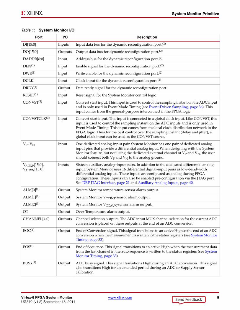
Table 1: System Monitor I/O
Port I/O Description
DI[15:0] Inputs Input data bus for the dynamic reconfiguration port.(2)
DO[15:0] Outputs Output data bus for dynamic reconfiguration port.(2)
DADDR[6:0] Input Address bus for the dynamic reconfiguration port.(2)
DEN(1) Input Enable signal for the dynamic reconfiguration port.(2)
DWE(1) Input Write enable for the dynamic reconfiguration port.(2)
DCLK Input Clock input for the dynamic reconfiguration port.(2)
DRDY(1) Output Data ready signal for the dynamic reconfiguration port.
RESET(1) Input Reset signal for the System Monitor control logic.
CONVST(3) Input Convert start input. This input is used to control the sampling instant on the ADC input and is only used in Event Mode Timing (see Event-Driven Sampling, page 36). This input comes from the general-purpose interconnect in the FPGA logic.
CONVSTCLK(3) Input Convert start input. This input is connected to a global clock input. Like CONVST, this input is used to control the sampling instant on the ADC inputs and is only used in Event Mode Timing. This input comes from the local clock distribution network in the FPGA logic. Thus for the best control over the sampling instant (delay and jitter), a global clock input can be used as the CONVST source.
VP, VN Input One dedicated analog-input pair. System Monitor has one pair of dedicated analog-input pins that provide a differential analog input. When designing with the System Monitor feature, but not using the dedicated external channel of VP and VN, the user should connect both VP and VN to the analog ground.
VAUXP[15:0],VAUXN[15:0]
Inputs Sixteen auxiliary analog-input pairs. In addition to the dedicated differential analog input, System Monitor uses 16 differential digital-input pairs as low-bandwidth differential analog inputs. These inputs are configured as analog during FPGA configuration. These inputs can also be enabled pre-configuration via the JTAG port. See DRP JTAG Interface, page 21 and Auxiliary Analog Inputs, page 40.
ALM[0](1) Output System Monitor temperature-sensor alarm output.
ALM[1](1) Output System Monitor VCCINT-sensor alarm output.
ALM[2](1) Output System Monitor VCCAUX-sensor alarm output.
OT Output Over-Temperature alarm output.
CHANNEL[4:0] Outputs Channel selection outputs. The ADC input MUX channel selection for the current ADC conversion is placed on these outputs at the end of an ADC conversion.
EOC(1) Output End of Conversion signal. This signal transitions to an active High at the end of an ADC conversion when the measurement is written to the status registers (see System Monitor Timing, page 33).
EOS(1) Output End of Sequence. This signal transitions to an active High when the measurement data from the last channel in the auto sequence is written to the status registers (see System Monitor Timing, page 33).
BUSY(1) Output ADC busy signal. This signal transitions High during an ADC conversion. This signal also transitions High for an extended period during an ADC or Supply Sensor calibration.
Send Feedback

10 www.xilinx.com Virtex-6 FPGA System MonitorUG370 (v1.2) September 18, 2014
Pre-Configuration Operation
User AttributesSystem Monitor functionality is configured by the Control registers (see Register File Interface, page 14). These Control registers can be initialized at design, using the Attributes listed in Table 2 and through the DRP at run time (see Control Registers, page 17).
Pre-Configuration OperationSystem Monitor starts operating in a safe mode of operation shortly after the FPGA is powered-up without performing a configuration.
Note: Holding INIT_B or PROG Low to delay configuration has no effect on System Monitor. System Monitor is available as soon as the Clear Configuration Memory step is complete, which is normally indicated by INIT_B going High. See the “Configuration Sequence” section in the Virtex-6 FPGA Configuration Guide for more information.
In this mode of operation, System Monitor operates in a sequence mode (see Channel Sequencer, page 25), monitoring the on-chip sensors: temperature, VCCINT, and VCCAUX. When operating in safe mode, System Monitor is not affected by any change in the FPGA’s configuration. System Monitor operates in safe mode prior to any configuration and during configuration (full and partial). It is possible to customize the System Monitor operation pre-configuration using the JTAG TAP. However, System Monitor only operates in safe mode during configuration and the contents of the System Monitor control registers
JTAGLOCKED(1) Output Used to indicate that a DRP port lock request has been made by the Joint Test Action Group (JTAG) interface (see DRP Arbitration, page 24).
JTAGMODIFIED(1) Output Used to indicate that a JTAG Write to the DRP has occurred.
JTAGBUSY(1) Output Used to indicate that a JTAG DRP transaction is in progress.
Notes: 1. Active-High signal.2. For some details on the timing for these DRP signals, consult Figure 16, page 38 and Table 19, page 39 or Chapter 5 (Dynamic
Reconfiguration Port) in the Virtex-6 FPGA Configuration Guide.3. Rising edge triggered signal.
Table 1: System Monitor I/O (Cont’d)
Port I/O Description
Table 2: System Monitor Attributes
Attribute NameControlRegisterAddress
Description
INIT_40 Configuration register 0 40h
System Monitor configuration registers (see Configuration Registers (40h to 42h), page 17).INIT_41 Configuration register 1 41h
INIT_42 Configuration register 2 42h
INIT_43 toINIT_47
Test registers 43h to 47h System Monitor Test registers for factory use only. The default initialization is 0000h.
INIT_48 toINIT_4F
Sequence registers 48h to 4Fh Sequence registers used to program the Channel Sequencer function in System Monitor (see Channel Sequencer, page 25).
INIT_50 toINIT_57
Alarm Limit registers 50h to 57h Alarm threshold registers for the System Monitor alarm function (see Automatic Alarms, page 29).
Send Feedback
Virtex-6 FPGA System Monitor www.xilinx.com 11UG370 (v1.2) September 18, 2014
Analog-to-Digital Converter
are overwritten when a full chip configuration is carried out. To enable auxiliary analog input channels during preconfiguration, see DRP JTAG Interface, page 21.
Because no system clock is available, System Monitor uses an internal clock oscillator pre-configuration. The full functionality of System Monitor is accessed pre-configuration through the JTAG Test Access Port (JTAG TAP) (see DRP JTAG Interface, page 21).
The JTAG interface provides full Read/Write access to the System Monitor register file interface. After power-up, the System Monitor functionality is customized, if required, through the JTAG TAP. The System Monitor functionality is also available through the JTAG TAP post configuration even if System Monitor has not been instantiated in a design. It is possible to access the System Monitor registers at any time using the JTAG TAP.
The basic connection requirements that ensure the System Monitor functionality is enabled are shown in Figure 4. For more information regarding power supply requirements, see Application Guidelines, page 45.
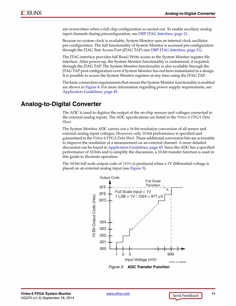
Analog-to-Digital ConverterThe ADC is used to digitize the output of the on-chip sensors and voltages connected to the external analog inputs. The ADC specifications are listed in the Virtex-6 FPGA Data Sheet.
The System Monitor ADC carries out a 16-bit resolution conversion of all sensor and external analog input voltages. However, only 10-bit performance is specified and guaranteed in the Virtex-6 FPGA Data Sheet. These additional conversion bits are accessable to improve the resolution of a measurement on an external channel. A more detailed discussion can be found in Application Guidelines, page 45. Since the ADC has a specified performance of 10-bits and to simplify the discussion, a 10-bit transfer function is used in this guide to illustrate operation.
The 10-bit full scale output code of 3FFh is produced when a 1V differential voltage is placed on an external analog input (see Figure 3).X-Ref Target - Figure 3
Figure 3: ADC Transfer Function
000
001
003
004
3FF
Output CodeFull ScaleTransition
3FE
3FD
002
1 2 3 999
Full Scale Input = 1V1 LSB = 1V / 1024 = 977 μV
10-B
it O
utpu
t Cod
e (H
ex)
UG370_03_060709Input Voltage (mV)
Send Feedback

12 www.xilinx.com Virtex-6 FPGA System MonitorUG370 (v1.2) September 18, 2014
Analog-to-Digital Converter
The System Monitor ADC has six dedicated pins (see Figure 4). Two of these pins provide a dedicated high-bandwidth, differential analog-input channel (VP , VN). Another two pins are used to access an external reference voltage (VREFP , VREFN). By using an external reference device, a reference voltage with a low-temperature coefficient (< 50 ppm/°C) can be supplied. This voltage is used to provide stable and accurate measurements over a wide temperature range. An internal reference circuit can also be selected by connecting VREFN and VREFP to analog ground (AGND). This internal reference is typically less accurate over a wide temperature range than an external reference. Performance using the internal reference circuit is specified in the Virtex-6 FPGA Data Sheet. For the most accurate measurements, an external reference IC is recommended.
The remaining analog pins (AVDD and AVSS) are used to decouple the power supply for the ADC analog circuits and provide a local AGND return for the ADC circuitry. The System Monitor connection diagrams (using the on-chip and external reference) are shown in Figure 4. For a more detailed discussion of required power supply connections and PC Board layout, see Application Guidelines, page 45.
In addition to on-chip sensors, the ADC is used to digitize external analog signals. There is one dedicated analog-input pin pair and 16 user-programmable analog-input pairs supplied for this purpose. The ADC has a true differential-sampling analog-input scheme, allowing the ADC to achieve a high degree of accuracy when digitizing both on-chip and external channels.
The ADC accommodates both unipolar and bipolar analog input signals (see Analog Inputs, page 39). The analog-input mode is selected by writing to the System Monitor configuration registers (see Configuration Registers (40h to 42h), page 17). In Single Channel mode, the configuration registers are also used to select the sampling modes of the ADC and the analog input channels such as, on-chip sensors and external analog-input channels.
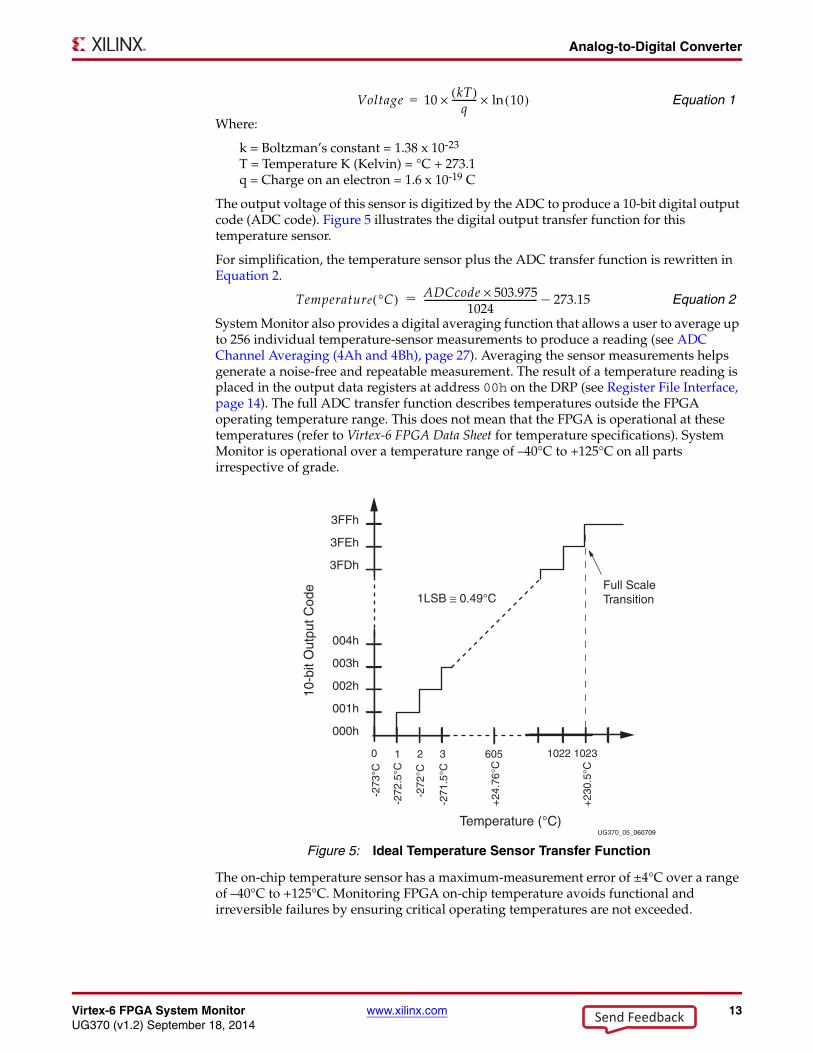
Temperature SensorSystem Monitor contains a temperature sensor that produces a voltage output that is proportional to the die temperature.
Equation 1 shows the output voltage of the temperature sensor.
X-Ref Target - Figure 4
Figure 4: System Monitor Dedicated Pins
ADC
1.25V ±0.2%50 ppm/°C
2.5V – 5V
AVDD
AVSS
VREFPVP
VN
VREFN
VCCAUX (2.5V ±5%)
VCCAUX (2.5V ±5%)
UG370_04_061009
External Reference
ADC
AVDD
AVSS
VREFPVP
VN
VREFN
On-Chip Reference
GNDFerrite for HF noise isolation
10nF 10nF
GNDFerrite for HF noise isolationPackage Pins
10nF
Send Feedback
Virtex-6 FPGA System Monitor www.xilinx.com 13UG370 (v1.2) September 18, 2014
Analog-to-Digital Converter
Equation 1
Where:
k = Boltzman’s constant = 1.38 x 10⁻²³
T = Temperature K (Kelvin) = °C + 273.1q = Charge on an electron = 1.6 x 10⁻¹⁹ C
The output voltage of this sensor is digitized by the ADC to produce a 10-bit digital output code (ADC code). Figure 5 illustrates the digital output transfer function for this temperature sensor.
For simplification, the temperature sensor plus the ADC transfer function is rewritten in Equation 2.
Equation 2
System Monitor also provides a digital averaging function that allows a user to average up to 256 individual temperature-sensor measurements to produce a reading (see ADC Channel Averaging (4Ah and 4Bh), page 27). Averaging the sensor measurements helps generate a noise-free and repeatable measurement. The result of a temperature reading is placed in the output data registers at address 00h on the DRP (see Register File Interface, page 14). The full ADC transfer function describes temperatures outside the FPGA operating temperature range. This does not mean that the FPGA is operational at these temperatures (refer to Virtex-6 FPGA Data Sheet for temperature specifications). System Monitor is operational over a temperature range of –40°C to +125°C on all parts irrespective of grade.
The on-chip temperature sensor has a maximum-measurement error of ±4°C over a range of –40°C to +125°C. Monitoring FPGA on-chip temperature avoids functional and irreversible failures by ensuring critical operating temperatures are not exceeded.
X-Ref Target - Figure 5
Figure 5: Ideal Temperature Sensor Transfer Function
Voltage 10 kT( )q----------- 10( )ln××=
Temperature °C( ) ADCcode 503.975×1024
--------------------------------------------------- 273.15–=
000h
001h
003h
004h
3FFh
10-b
it O
utpu
t Cod
e Full ScaleTransition
3FEh
3FDh
002h
10 2 3 605 10231022
Temperature (°C)
+23
0.5°
C
+24
.76°
C
-273
°C
-272
.5°C
-272
°C
-271
.5°C
1LSB ≅ 0.49°C
UG370_05_060709
Send Feedback

14 www.xilinx.com Virtex-6 FPGA System MonitorUG370 (v1.2) September 18, 2014
Register File Interface
Power Supply SensorSystem Monitor also includes on-chip sensors allowing a user to monitor the FPGA power-supply voltages using the ADC. The sensors sample and attenuate (by a factor of three) the power supply voltages VCCINT and VCCAUX on the package power supply balls. Figure 6 shows the power-supply sensor transfer function after digitizing by the ADC. The Power Supply sensor can be used to measure voltages in the range 0V to VCCAUX + 5% with a resolution of approximately 3 mV:
Supply Voltage (Volts) = (ADC Code / 1024) x 3V Equation 3
Similar to the temperature sensor, System Monitor provides a digital-averaging function for the power supply measurements. Thus, up to 256 measurements of a sensor output are used to generate a single reading. The power-supply measurement results for VCCINT and VCCAUX are stored in the data registers at DRP addresses 01h and 02h, respectively (see Status Registers, page 15).
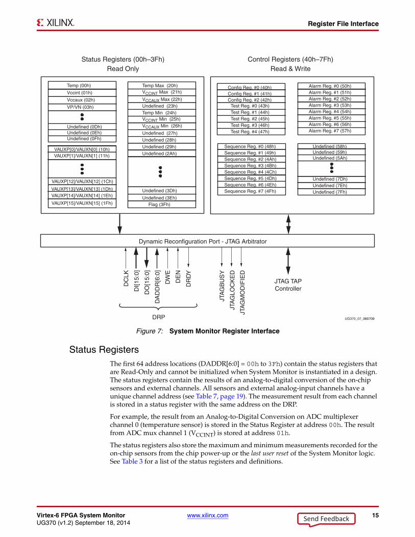
Register File InterfaceFigure 7 illustrates the System Monitor register file interface. All registers in the register file interface are accessible through the DRP. The DRP can be accessed via a fabric port or the JTAG TAP. Access is governed by an arbitrator (see DRP Arbitration, page 24). The DRP allows the user to access up to 128 16-bit registers (DADDR[6:0] = 00h to 7Fh) from the FPGA logic. The first 64 access locations (DADDR[6:0] = 00h to 3Fh) are read-only and contain the status registers (see Status Registers). The Control registers are located at addresses 40h to 7Fh (see Control Registers, page 17) and are readable or writable via the DRP. The DRP timing is shown in Figure 16, page 38. For a detailed description of the DRP timing please refer to the Virtex-6 FPGA Configuration Guide. For more information on the JTAG DRP interface, see DRP JTAG Interface, page 21.
X-Ref Target - Figure 6
Figure 6: Ideal Power Supply Transfer Function
10-B
it O
utpu
t Cod
e
Supply Voltage (Volts)
Output Code
Full ScaleTransition
2.93
mV
5.86
mV
8.79
mV
1.00
V
2.50
V
2.99
7V
2.99
4V
1 LSB = 2.93 mV
000h
001h
003h
004h
3FFh
3FEh
355h
155h
002h
UG370_06_060709
Send Feedback
Virtex-6 FPGA System Monitor www.xilinx.com 15UG370 (v1.2) September 18, 2014
Register File Interface
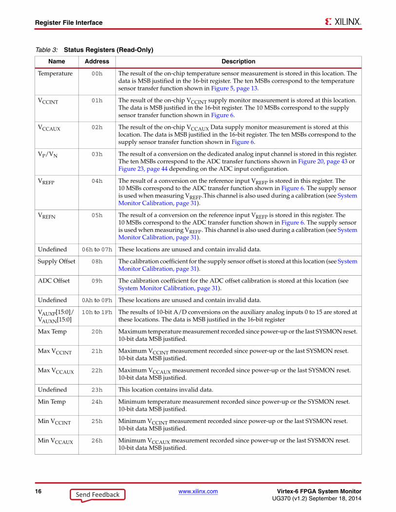
Status RegistersThe first 64 address locations (DADDR[6:0] = 00h to 3Fh) contain the status registers that are Read-Only and cannot be initialized when System Monitor is instantiated in a design. The status registers contain the results of an analog-to-digital conversion of the on-chip sensors and external channels. All sensors and external analog-input channels have a unique channel address (see Table 7, page 19). The measurement result from each channel is stored in a status register with the same address on the DRP.
For example, the result from an Analog-to-Digital Conversion on ADC multiplexer channel 0 (temperature sensor) is stored in the Status Register at address 00h. The result from ADC mux channel 1 (VCCINT) is stored at address 01h.
The status registers also store the maximum and minimum measurements recorded for the on-chip sensors from the chip power-up or the last user reset of the System Monitor logic. See Table 3 for a list of the status registers and definitions.
X-Ref Target - Figure 7
Figure 7: System Monitor Register Interface
DI[1
5:0]
DO
[15:
0]
DA
DD
R[6
:0]
DC
LK
JTA
GB
US
Y
JTA
GLO
CK
ED
JTA
GM
OD
IFIE
D
DW
E
DE
N
DR
DY
Config Reg. #0 (40h)Config Reg. #1 (41h)Config Reg. #2 (42h)
Test Reg. #1 (44h)Test Reg. #0 (43h)
Test Reg. #4 (47h)
Test Reg. #2 (45h)Test Reg. #3 (46h)
Alarm Reg. #0 (50h)Alarm Reg. #1 (51h)Alarm Reg. #2 (52h)
Alarm Reg. #4 (54h)Alarm Reg. #3 (53h)
Alarm Reg. #7 (57h)
Alarm Reg. #5 (55h)Alarm Reg. #6 (56h)
Undefined (58h)Undefined (59h)Undefined (5Ah)
Undefined (7Fh)
Undefined (7Dh)Undefined (7Eh)
Sequence Reg. #0 (48h)Sequence Reg. #1 (49h)Sequence Reg. #2 (4Ah)
Sequence Reg. #4 (4Ch)Sequence Reg. #3 (4Bh)
Sequence Reg. #7 (4Fh)
Sequence Reg. #5 (4Dh)Sequence Reg. #6 (4Eh)
Temp (00h)
Vccint (01h)
Vccaux (02h)
VP/VN (03h)
Undefined (0Fh)
VAUXP[1]/VAUXN[1] (11h)
VCCINT Max (21h)
VCCAUX Max (22h)Undefined (23h)
Temp Max (20h)
VCCINT Min (25h)VCCAUX Min (26h)
Undefined (27h)
Temp Min (24h)
VAUXP[0]/VAUXN[0] (10h)
Undefined (0Eh)Undefined (0Dh)
Control Registers (40h–7Fh)Read & WriteRead Only
Status Registers (00h–3Fh)
Dynamic Reconfiguration Port - JTAG Arbitrator
Undefined (28h)Undefined (29h)Undefined (2Ah)
Flag (3Fh)Undefined (3Eh)
Undefined (3Dh)VAUXP[13]/VAUXN[13] (1Dh)
VAUXP[12]/VAUXN[12] (1Ch)
VAUXP[14]/VAUXN[14] (1Eh)
VAUXP[15]/VAUXN[15] (1Fh)
DRP
JTAG TAPController
UG370_07_060709
Send Feedback
16 www.xilinx.com Virtex-6 FPGA System MonitorUG370 (v1.2) September 18, 2014
Register File Interface
Table 3: Status Registers (Read-Only)
Name Address Description
Temperature 00h The result of the on-chip temperature sensor measurement is stored in this location. The data is MSB justified in the 16-bit register. The ten MSBs correspond to the temperature sensor transfer function shown in Figure 5, page 13.
VCCINT 01h The result of the on-chip VCCINT supply monitor measurement is stored at this location. The data is MSB justified in the 16-bit register. The 10 MSBs correspond to the supply sensor transfer function shown in Figure 6.
VCCAUX 02h The result of the on-chip VCCAUX Data supply monitor measurement is stored at this location. The data is MSB justified in the 16-bit register. The ten MSBs correspond to the supply sensor transfer function shown in Figure 6.
VP/VN 03h The result of a conversion on the dedicated analog input channel is stored in this register. The ten MSBs correspond to the ADC transfer functions shown in Figure 20, page 43 or Figure 23, page 44 depending on the ADC input configuration.
VREFP 04h The result of a conversion on the reference input VREFP is stored in this register. The 10 MSBs correspond to the ADC transfer function shown in Figure 6. The supply sensor is used when measuring VREFP.This channel is also used during a calibration (see System Monitor Calibration, page 31).
VREFN 05h The result of a conversion on the reference input VREFP is stored in this register. The 10 MSBs correspond to the ADC transfer function shown in Figure 6. The supply sensor is used when measuring VREFP. This channel is also used during a calibration (see System Monitor Calibration, page 31).
Undefined 06h to 07h These locations are unused and contain invalid data.
Supply Offset 08h The calibration coefficient for the supply sensor offset is stored at this location (see System Monitor Calibration, page 31).
ADC Offset 09h The calibration coefficient for the ADC offset calibration is stored at this location (see System Monitor Calibration, page 31).
Undefined 0Ah to 0Fh These locations are unused and contain invalid data.
VAUXP[15:0]/VAUXN[15:0]
10h to 1Fh The results of 10-bit A/D conversions on the auxiliary analog inputs 0 to 15 are stored at these locations. The data is MSB justified in the 16-bit register
Max Temp 20h Maximum temperature measurement recorded since power-up or the last SYSMON reset. 10-bit data MSB justified.
Max VCCINT 21h Maximum VCCINT measurement recorded since power-up or the last SYSMON reset. 10-bit data MSB justified.
Max VCCAUX 22h Maximum VCCAUX measurement recorded since power-up or the last SYSMON reset. 10-bit data MSB justified.
Undefined 23h This location contains invalid data.
Min Temp 24h Minimum temperature measurement recorded since power-up or the SYSMON reset. 10-bit data MSB justified.
Min VCCINT 25h Minimum VCCINT measurement recorded since power-up or the last SYSMON reset. 10-bit data MSB justified.
Min VCCAUX 26h Minimum VCCAUX measurement recorded since power-up or the last SYSMON reset. 10-bit data MSB justified.
Send Feedback

Virtex-6 FPGA System Monitor www.xilinx.com 17UG370 (v1.2) September 18, 2014
Register File Interface
Flag Register
The Flag Register is shown in Figure 8. The bit definitions are described in Table 4.
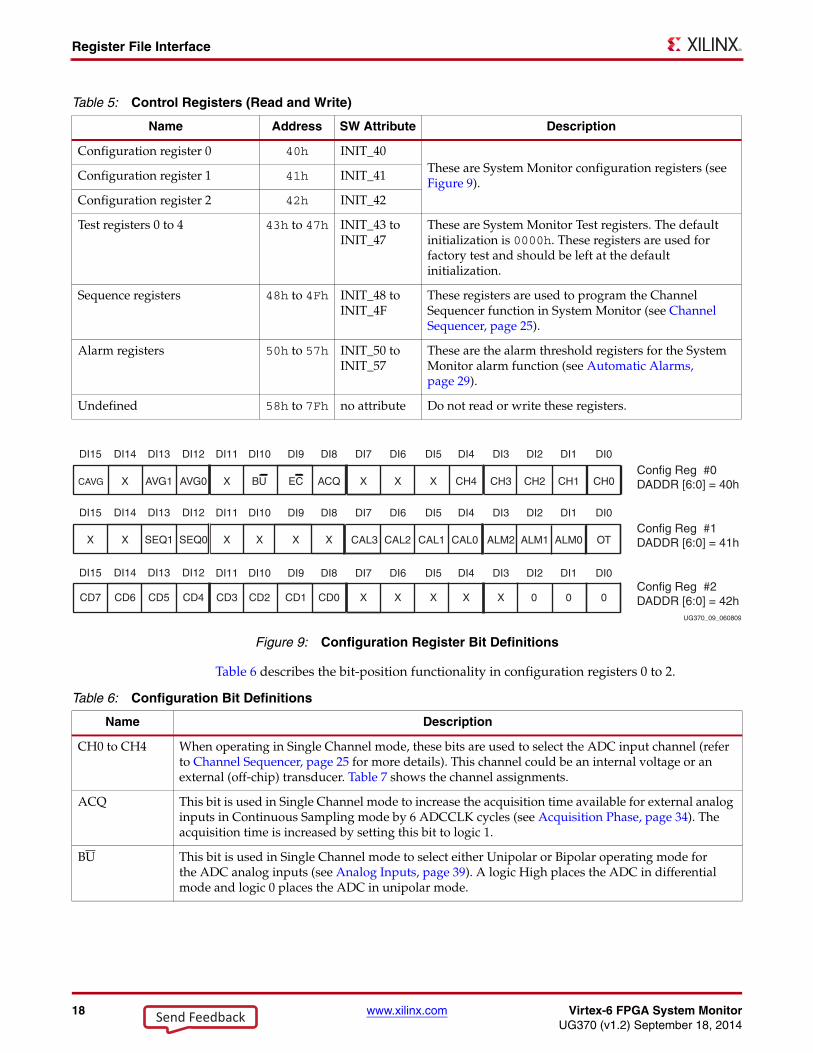
Control RegistersThe System Monitor control registers (Table 5) are located at addresses 40h to 7Fh. These registers are used to configure the System Monitor operation. System Monitor functionality (ADC operating modes, Channel Sequencer, and Alarm limits) is controlled through these registers. System Monitor functionality is explained in System Monitor Control Logic, page 25.
The control registers are initialized using the SYSMON attributes when System Monitor is instantiated in a design. This means that System Monitor can be configured to start in a predefined mode after FPGA configuration.
Configuration Registers (40h to 42h)
The first three registers in the control register block are used to configure the System Monitor operating modes. These registers are known as System Monitor configuration registers. The configuration registers bit definitions are illustrated in Figure 9. The Xs in Figure 9 define these bit positions as don’t cares. Bits 0, 1, and 2 in configuration register 2 (42h) should always be set to 0.
The configuration registers are modifiable through the DRP after the FPGA has been configured. For example, a soft microprocessor or state machine can be used to alter the contents of the System Monitor control registers at any time during normal operation.
Undefined 27h to 3Eh These locations are unused and contain invalid data.
Flag 3Fh This register contains general status information - see Figure 8.
Table 3: Status Registers (Read-Only) (Cont’d)
Name Address Description
X-Ref Target - Figure 8
Figure 8: Flag Register
Table 4: Flag Register Definitions
Name Description
OT This bit reflects the status of the Over Temperature logic output
DIS When this bit is a logic 1, the System Monitor is disabled by connecting the supplies and reference inputs to AGND.
REF When this bit is a logic 1, the System Monitor ADC is using the internal voltage reference. When it is a logic 0, then the external reference is being used.
Flag RegisterDADDR [6:0] = 3Fh
DI0DI1DI2DI3DI4DI5DI6DI7DI8DI9DI10DI11DI12DI13DI14DI15
X OTDIS X X XX XXX X REFX X XX
UG370_08_060709
Send Feedback
18 www.xilinx.com Virtex-6 FPGA System MonitorUG370 (v1.2) September 18, 2014
Register File Interface
Table 6 describes the bit-position functionality in configuration registers 0 to 2.
Table 5: Control Registers (Read and Write)
Name Address SW Attribute Description
Configuration register 0 40h INIT_40These are System Monitor configuration registers (see Figure 9).
Configuration register 1 41h INIT_41
Configuration register 2 42h INIT_42
Test registers 0 to 4 43h to 47h INIT_43 toINIT_47
These are System Monitor Test registers. The default initialization is 0000h. These registers are used for factory test and should be left at the default initialization.
Sequence registers 48h to 4Fh INIT_48 toINIT_4F
These registers are used to program the Channel Sequencer function in System Monitor (see Channel Sequencer, page 25).
Alarm registers 50h to 57h INIT_50 toINIT_57
These are the alarm threshold registers for the System Monitor alarm function (see Automatic Alarms, page 29).
Undefined 58h to 7Fh no attribute Do not read or write these registers.
X-Ref Target - Figure 9
Figure 9: Configuration Register Bit Definitions
Config Reg #1DADDR [6:0] = 41h
Config Reg #2DADDR [6:0] = 42h
Config Reg #0DADDR [6:0] = 40h
DI0DI1DI2DI3DI4DI5DI6DI7DI8DI9DI10DI11DI12DI13DI14DI15
CH4 CH3 CH2 CH1 CH0ACQ X XXXXCAVG AVG1 AVG0 BU EC
UG370_09_060809
DI12DI13DI14DI15 DI0DI1DI2DI3DI4DI5DI6DI7DI8DI9DI10DI11
ALM0ALM1ALM2 OTSEQ1 SEQ0 XX XXXX CAL0CAL1CAL2CAL3
DI12DI13DI14DI15 DI0DI1DI2DI3DI4DI5DI6DI7DI8DI9DI10DI11
CD0 0 0CD1CD2 XX X 0CD3CD4CD5CD6CD7 X X
Table 6: Configuration Bit Definitions
Name Description
CH0 to CH4 When operating in Single Channel mode, these bits are used to select the ADC input channel (refer to Channel Sequencer, page 25 for more details). This channel could be an internal voltage or an external (off-chip) transducer. Table 7 shows the channel assignments.
ACQ This bit is used in Single Channel mode to increase the acquisition time available for external analog inputs in Continuous Sampling mode by 6 ADCCLK cycles (see Acquisition Phase, page 34). The acquisition time is increased by setting this bit to logic 1.
BU This bit is used in Single Channel mode to select either Unipolar or Bipolar operating mode for the ADC analog inputs (see Analog Inputs, page 39). A logic High places the ADC in differential mode and logic 0 places the ADC in unipolar mode.
Send Feedback
Virtex-6 FPGA System Monitor www.xilinx.com 19UG370 (v1.2) September 18, 2014
Register File Interface
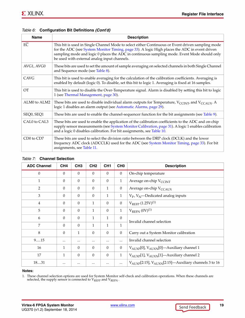
EC This bit is used in Single Channel Mode to select either Continuous or Event driven sampling mode for the ADC (see System Monitor Timing, page 33). A logic High places the ADC in event driven sampling mode and logic 0 places the ADC in continuous sampling mode. Event Mode should only be used with external analog input channels.
AVG1, AVG0 These bits are used to set the amount of sample averaging on selected channels in both Single Channel and Sequence mode (see Table 8).
CAVG This bit is used to enable averaging for the calculation of the calibration coefficients. Averaging is enabled by default (logic 0). To disable, set this bit to logic 1. Averaging is fixed at 16 samples.
OT This bit is used to disable the Over-Temperature signal. Alarm is disabled by setting this bit to logic 1 (see Thermal Management, page 30).
ALM0 to ALM2 These bits are used to disable individual alarm outputs for Temperature, VCCINT, and VCCAUX. A logic 1 disables an alarm output (see Automatic Alarms, page 29).
SEQ0, SEQ1 These bits are used to enable the channel-sequencer function for the bit assignments (see Table 9).
CAL0 to CAL3 These bits are used to enable the application of the calibration coefficients to the ADC and on-chip supply sensor measurements (see System Monitor Calibration, page 31). A logic 1 enables calibration and a logic 0 disables calibration. For bit assignments, see Table 10.
CD0 to CD7 These bits are used to select the division ratio between the DRP clock (DCLK) and the lower frequency ADC clock (ADCCLK) used for the ADC (see System Monitor Timing, page 33). For bit assignments, see Table 11.
Table 7: Channel Selection
ADC Channel CH4 CH3 CH2 CH1 CH0 Description
0 0 0 0 0 0 On-chip temperature
1 0 0 0 0 1 Average on-chip VCCINT
2 0 0 0 1 0 Average on-chip VCCAUX
3 0 0 0 1 1 VP, VN—Dedicated analog inputs
4 0 0 1 0 0 VREFP (1.25V)(1)
5 0 0 1 0 1 VREFN (0V)(1)
6 0 0 1 1 0Invalid channel selection
7 0 0 1 1 1
8 0 1 0 0 0 Carry out a System Monitor calibration
9.....15 ... ... ... ... ... Invalid channel selection
16 1 0 0 0 0 VAUXP[0], VAUXN[0]—Auxiliary channel 1
17 1 0 0 0 1 VAUXP[1], VAUXN[1]—Auxiliary channel 2
18....31 ... ... ... ... ... VAUXP[2:15], VAUXN[2:15]—Auxiliary channels 3 to 16
Notes: 1. These channel selection options are used for System Monitor self-check and calibration operations. When these channels are
selected, the supply sensor is connected to VREFP and VREFN .
Table 6: Configuration Bit Definitions (Cont’d)
Name Description
Send Feedback

20 www.xilinx.com Virtex-6 FPGA System MonitorUG370 (v1.2) September 18, 2014
Register File Interface
Table 8: Averaging Filter
AVG1 AVG0 Function
0 0 No averaging
0 1 Average 16 samples
1 0 Average 64 samples
1 1 Average 256 samples
Table 9: Channel Sequencer Operation
SEQ1 SEQ0 Function
0 0 Default safe mode (see Pre-Configuration Operation, page 10)
0 1 One pass through sequence(1)
1 0 Continuous cycling of sequence
Notes: 1. To restart the sequence, the sequencer settings must be restarted. For example, setting
the channel sequencer to the single channel settings(SEQ[1:0] = 11) before setting the sequence mode back to the one pass through sequence (SEQ[1:0] = 01).
Table 10: Calibration Enables
Name Description
CAL0 ADC offset correction enable
CAL1 ADC offset and gain correction enable
CAL2 Supply Sensor offset correction enable
CAL3 Supply Sensor offset and gain correction enable
Table 11: DCLK Division Selection(1)
CD7 CD6 CD5 CD4 CD3 CD2 CD1 CD0 Division
0 0 0 0 0 0 0 0 2
0 0 0 0 0 0 0 1 2
0 0 0 0 0 0 1 0 2
0 0 0 0 0 0 1 1 3
0 0 0 0 0 1 0 0 4
– – – – – – – – ...
1 1 1 1 1 1 1 0 254
1 1 1 1 1 1 1 1 255
Notes: 1. Minimum division ratio is 2, for example, ADCCLK = DCLK/2.
Send Feedback

Virtex-6 FPGA System Monitor www.xilinx.com 21UG370 (v1.2) September 18, 2014
Register File Interface
Test Registers (43h to 47h)
These registers are intended for factory test purposes only and have a default status of zero. The user must not write to these registers.
Channel Sequencer Registers (48h to 4Fh)
These registers are used to program the channel sequencer functionality (see Channel Sequencer, page 25).
Alarm Registers (50h to 57h)
These registers are used to program the alarm thresholds for the automatic alarms on the internally monitored channels, temperature, VCCINT , and VCCAUX (see Automatic Alarms, page 29).
DRP JTAG InterfaceSystem Monitor uses a full JTAG interface extension to the System Monitor DRP interface. This allows Read/Write access to the System Monitor DRP through the existing on-chip JTAG infrastructure. No instantiation is required to access the System Monitor DRP interface over JTAG. A Boundary-Scan instruction (10-bit instruction = 1111110111) called SYSMON has been added to Virtex-6 devices to allow access to the System Monitor DRP through the JTAG TAP. All System Monitor JTAG instructions are 32-bits in length. For more information on the Virtex-6 FPGA Boundary-Scan instructions and usage, see the Virtex-6 FPGA Configuration Guide. Read and Write operations using the System Monitor JTAG DRP interface are described in the next sections. Users unfamiliar with basic JTAG functionality should understand the JTAG standard (IEEE1149.1) before proceeding.
System Monitor DRP JTAG Write Operation
Figure 10 shows a timing diagram for a Write operation to the SYSMON DRP through the JTAG TAP. The DRP is accessed through the System Monitor Data register (SYSMON DR). Before the SYSMON DR is accessed, the instruction register (IR) must first be loaded with the SYSMON instruction. The Controller is first placed in the IR-scan mode, and the SYSMON instruction is shifted to the IR.
After the SYSMON instruction is loaded, all data register (DR)-scan operations are carried out on the SYSMON DR. When the data shifted into SYSMON DR is a JTAG DRP Write command, the SYSMON DRP arbitrator carries out a DRP write. The format of this Write command is described in JTAG DRP Commands, page 23. The SYSMON DR contents are transferred to the SYSMON DRP arbitrator (see DRP Arbitration, page 24) during the Update-DR state. After the Update-DR state, the arbitrator manages the new data transfer to the System Monitor DRP register. This takes up to six DRP Clock (DCLK) cycles if a DRP access from the fabric is already in progress.
During the Capture-DR phase (just before data is shifted into the SYSMON DR), DRP data is captured from the arbitrator. Depending on the last JTAG DRP command, this data could be old data, previously written to the DRP or requested new Read data (see System Monitor JTAG DRP Read Operation, page 22). This captured data is shifted out (LSB first) on DO as the new JTAG DRP command is shifted in. The 16 LSBs of this 32-bit word contain the JTAG DRP data. The 16 MSBs are set to zero.
If multiple writes to the SYSMON DR are taking place, it might be necessary to idle the TAP Controller for several TCK cycles before advancing to the next write operation. This is illustrated in Figure 10. The idle cycles allow the arbitrator to complete the Write operation
Send Feedback

22 www.xilinx.com Virtex-6 FPGA System MonitorUG370 (v1.2) September 18, 2014
Register File Interface
to the System Monitor DRP register. If DCLK is running approximately 6 x TCK, these idle states are not necessary. However, inserting ten or so idle states ensures all transfers are inherently safe.
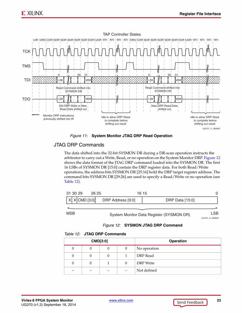
System Monitor JTAG DRP Read Operation
Figure 11 shows the timing for a SYSMON DR Read operation. The IR should contain the DR-scan operation SYSMON instruction. A JTAG Read from the System Monitor DRP is a two-step operation.
• First, the SYSMON DR is loaded with the Read DRP instruction. This instruction is transferred to the arbitrator during the Update-DR state and then the arbitrator reads the selected DRP register and stores the newly read 16-bit data. This operation takes several DCLK cycles to complete.
• During the DR-Capture phase of the next DR-scan, newly read data is transferred from the arbitrator to the SYSMON DR. This 16-bit data (stored in the 16 LSBs of the 32-bit word) is then shifted out on TDO during the subsequent shift operation (see Figure 11). The timing diagram shows a number of idle states at the end of the first DR-scan operation, allowing the arbitrator enough time to fetch the System Monitor DRP data.
As mentioned previously, if the DCLK frequency is significantly faster than the TCK, these idle states might not be required.
Note: Implementing a DR-scan operation before the arbitrator has completed the DRP-read operation results in old DRP data being transferred to the SYSMON DR during the DR-capture phase.
To ensure reliable operation over all operating clock frequencies, a minimum of ten Run-Test-Idle (RTI) states should be inserted. Multiple Read operations can be pipelined, as shown in Figure 11. Thus, as the result of a read operation is being shifted out of the SYSMON DR, an instruction for the next read can be shifted in.
X-Ref Target - Figure 10
Figure 10: System Monitor JTAG DRP Write Operation
TAP Controller States
TCK
TMS
TDI
TDO
0 9 0 3130
MSB
MSB MSB
MSB
LSB
LSB
LSB
LSB
Load IR with SYSMON insructions
Idle between successiveWrites to allow DRP Write
operation to finish
Old DRP Write or New Read Data shifted out
Write DRP Command shifted intoSYSMON DR
TLR TLR RTI RTI RTI RTIDRS DRSDRSIRS CIR CDR CDRSIR SIR SIR SIR SDR SDR SDRSDR SDREIR EDR UDRUIR
UG370_10_060809
Send Feedback
Virtex-6 FPGA System Monitor www.xilinx.com 23UG370 (v1.2) September 18, 2014
Register File Interface
JTAG DRP Commands
The data shifted into the 32-bit SYSMON DR during a DR-scan operation instructs the arbitrator to carry out a Write, Read, or no operation on the System Monitor DRP. Figure 12 shows the data format of the JTAG DRP command loaded into the SYSMON DR. The first 16 LSBs of SYSMON DR [15:0] contain the DRP register data. For both Read/Write operations, the address bits SYSMON DR [25:16] hold the DRP target register address. The command bits SYSMON DR [29:26] are used to specify a Read/Write or no operation (see Table 12).
X-Ref Target - Figure 11
Figure 11: System Monitor JTAG DRP Read Operation
TCK
TMS
TDI
TDO
Idle to allow DRP Read to complete beforeshifting out result
Idle to allow DRP Read to complete beforeshifting out result
0 3130
MSB
MSB
LSB
LSB
Old DRP Write or New Read Data shfited out
Read Command shifted into SYSMON DR
0 3130
MSB
MSB
LSB
LSB
New DRP Read Datashifted out
Read Command shifted into SYSMON DR
RTIUIR RTI RTI RTI RTI RTI RTIDRS CDR SDR SDR SDRSDR SDR EDR UDR RTI DRS CDR SDR SDR SDRSDR SDR EDR UDR
Monitor DRP instructionspreviously shifted into IR
TAP Controller States
UG370_11_060809
X-Ref Target - Figure 12
Figure 12: SYSMON JTAG DRP Command
Table 12: JTAG DRP Commands
CMD[3:0] Operation
0 0 0 0 No operation
0 0 0 1 DRP Read
0 0 1 0 DRP Write
– – – – Not defined
151625262931 30 0
DRP Data [15:0]CMD [3:0]
MSB LSB
DRP Address [9:0]
System Monitor Data Register (SYSMON DR)
X X
UG370_12_060809
Send Feedback
24 www.xilinx.com Virtex-6 FPGA System MonitorUG370 (v1.2) September 18, 2014
Register File Interface
It is also possible to enable the auxiliary analog input channel pre-configuration of the FPGA, allowing external analog voltages (on the PCB) to be monitored using the JTAG TAP before configuration. The auxiliary channels are enabled by writing 0001h to DRP address 02h. This address lies within the read-only status register address space and normally holds the result of a VCCAUX measurement. However, a write to this address enables the auxiliary inputs.
Note: This function only works prior to configuration. Post configuration, these inputs must be explicitly instantiated in the design.
DRP Arbitration
Because the DRP registers are accessed from two different ports (interconnect and JTAG TAP) access must be carefully managed. An arbitrator has been implemented to manage potential conflicts between the fabric and JTAG port. Arbitration is managed on a per transaction basis (a transaction is a single Read/Write operation to the DRP). The arbitration rules are as follows:
• A JTAG transaction cannot be interrupted by the fabric. The fabric transaction is queued by the arbitrator until the JTAG transaction has finished, and then the fabric transaction is completed.
• A JTAG transaction cannot interrupt a fabric transaction already in progress. As soon as the fabric transaction is finished, then the JTAG transaction is completed.
Three status signals are provided to help manage access through the interconnect when the JTAG port is also being used.
JTAGBUSY
This signal becomes active during the update phase of a DRP transaction through the JTAG TAP. The signal resets when the JTAG SYSMON DR transaction is completed. Each Read/Write to the SYSMON DR is treated as an individual transaction. If DRP access initiates through the interconnect port when JTAGBUSY is High, then the arbitrator queues this request for a Read/Write through the fabric. DRDY does not go active until JTAGBUSY transitions Low and the interconnect transaction is completed. A second DRP access through the fabric must not be initiated until the DRDY for the initial access becomes active and indicates the Read/Write was successful. If an interconnect access is in progress when a JTAG DRP transaction initiates, the interconnect access is completed before the JTAG transaction.
JTAGMODIFIED
Whenever there is a JTAG Write (JTAG Reads typically occur more often) to any register in the DRP, the application (FPGA) must be notified about the potential change of configuration. Thus, a signal called JTAGMODIFIED transitions High after a JTAG Write. A subsequent DRP Read/Write resets the signal.
JTAGLOCKED
In some cases, it is simpler for the JTAG user to take DRP ownership for a period by locking out access through the interconnect. This is useful in a diagnostic situation where a large number of DRP registers are modified through the JTAG TAP. When a JTAGLOCKED request is made, the JTAGLOCKED signal transitions to an active High. The signal remains High until the port is unlocked again. No read or write access is possible via the DRP fabric port when the JTAGLOCKED signal is High. The
Send Feedback
Virtex-6 FPGA System Monitor www.xilinx.com 25UG370 (v1.2) September 18, 2014
System Monitor Control Logic
JTAGLOCKED signal is activated by writing 0001h to DRP address 00h. The JTAGLOCKED signal is reset again by writing 0000h to DRP address 00h.
System Monitor Control LogicMany of the most commonly used system monitoring functions are implemented in the System Monitor control logic. Common functions include:
• Channel sequencer
• Measurement averaging
• Maximum and minimum internal sensor measurements
• Automatic alarms on internal sensors
• Sensor and ADC calibration
The control logic also decodes the configuration registers to configure the ADC sampling modes (see System Monitor Timing, page 33) and external analog-input configuration (see Analog Inputs, page 39).
Channel SequencerWhen bits SEQ1 and SEQ0 in Control Register 41h are set to logic 1 (see Table 9, page 20), System Monitor operates in Single Channel mode. In this mode, the user must select the channel for Analog-to-Digital conversion by writing to the bit locations CH0 to CH4 in control register 40h. Operating modes for Single Channel mode, such as analog input mode (BU) and acquisition time (ACQ), must also be set by writing to Control Register 40h. In applications where many channels need to be monitored, this can mean a significant overhead for the microprocessor or other controller. To automate this task, a function called the Channel Sequencer is provided.
The Channel Sequencer provides a method for the user to set up a predefined sequence of channels (both internal and external) to be automatically monitored. The Channel Sequencer function is implemented using eight control registers from address 48h to 4Fh on the DRP (see Control Registers, page 17). These eight registers can be viewed as four pairs of 16-bit registers. Each pair of registers controls one aspect of the sequencer functionality. Individual bits in each pair of registers (32 bits) enable a specific functionality for a particular ADC channel. The four pairs of registers are:
• ADC channel selection (48h and 49h)
• ADC channel averaging enables (4Ah and 4Bh)
• ADC channel analog-input mode (4Ch and 4Dh)
• ADC channel acquisition time (4Eh and 4Fh)
System Monitor only operates in Continuous Sampling mode (see Continuous Sampling, page 34) when the automatic channel sequencer is enabled. Sequencer mode is enabled by using bits SEQ1 and SEQ0 in Configuration register 1 (see Configuration Registers (40h to 42h), page 17). The Channel Sequencer registers should be initialized by the user when System Monitor is instantiated in a design (see System Monitor Primitive, page 8). The Channel Sequencer can also be reconfigured via the DRP at run time. The Sequencer must first be disabled by writing to bits SEQ1 and SEQ0 before writing to any of the Channel Sequencer registers. It is recommended the System Monitor is placed in safe mode by writing zeros to SEQ0 and SEQ1 while updating the Control Registers. System Monitor is automatically reset whenever SEQ1 and SEQ0 are changed. The current status register
Send Feedback
26 www.xilinx.com Virtex-6 FPGA System MonitorUG370 (v1.2) September 18, 2014
System Monitor Control Logic
contents are not reset at this time. Restarting the sequencer by writing to bits SEQ1 and SEQ0 resets all channel averaging (see ADC Channel Averaging (4Ah and 4Bh), page 27).
ADC Channel Selection (48h and 49h)
The ADC channel selection registers enable and disable a channel in the automatic monitoring sequence. The bit definitions for these registers are described in Table 13 and Table 14. The two 16-bit registers are used to enable or disable the associated channels. A logic 1 enables a particular channel in the sequence. The sequence order is fixed starting from the LSB (bit 0) of register 48h and ending with the MSB (bit 15) of register 49h.
Table 13: Sequencer ADC Channel Selection, Control Register 48h
SequenceNumber
BitADC
ChannelDescription
1 0 8 System Monitor calibration(1)
1 9
Invalid channel selection
2 10
3 11
4 12
5 13
6 14
7 15
2 8 0 On-Chip temperature
3 9 1 Average On-Chip VCCINT
4 10 2 Average On-Chip VCCAUX
5 11 3 VP, VN—Dedicated analog inputs
6 12 4 VREFP (1.25V)
7 13 5 VREFN (0V)
14 6Invalid channel selection
15 7
Notes: 1. See the ADC Channel Averaging (4Ah and 4Bh) section for further details on how calibration is done
in an averaged sequence.
Table 14: Sequencer ADC Channel Selection, Control Register 49h
SequenceNumber
BitADC
ChannelDescription
8 0 16 VAUXP[0],VAUXN[0]—Auxiliary channel 1
9 1 17 VAUXP[1],VAUXN[1]—Auxiliary channel 2
10 2 18 VAUXP[2],VAUXN[2]—Auxiliary channel 3
11 3 19 VAUXP[3],VAUXN[3]—Auxiliary channel 4
Send Feedback
Virtex-6 FPGA System Monitor www.xilinx.com 27UG370 (v1.2) September 18, 2014
System Monitor Control Logic
ADC Channel Averaging (4Ah and 4Bh)
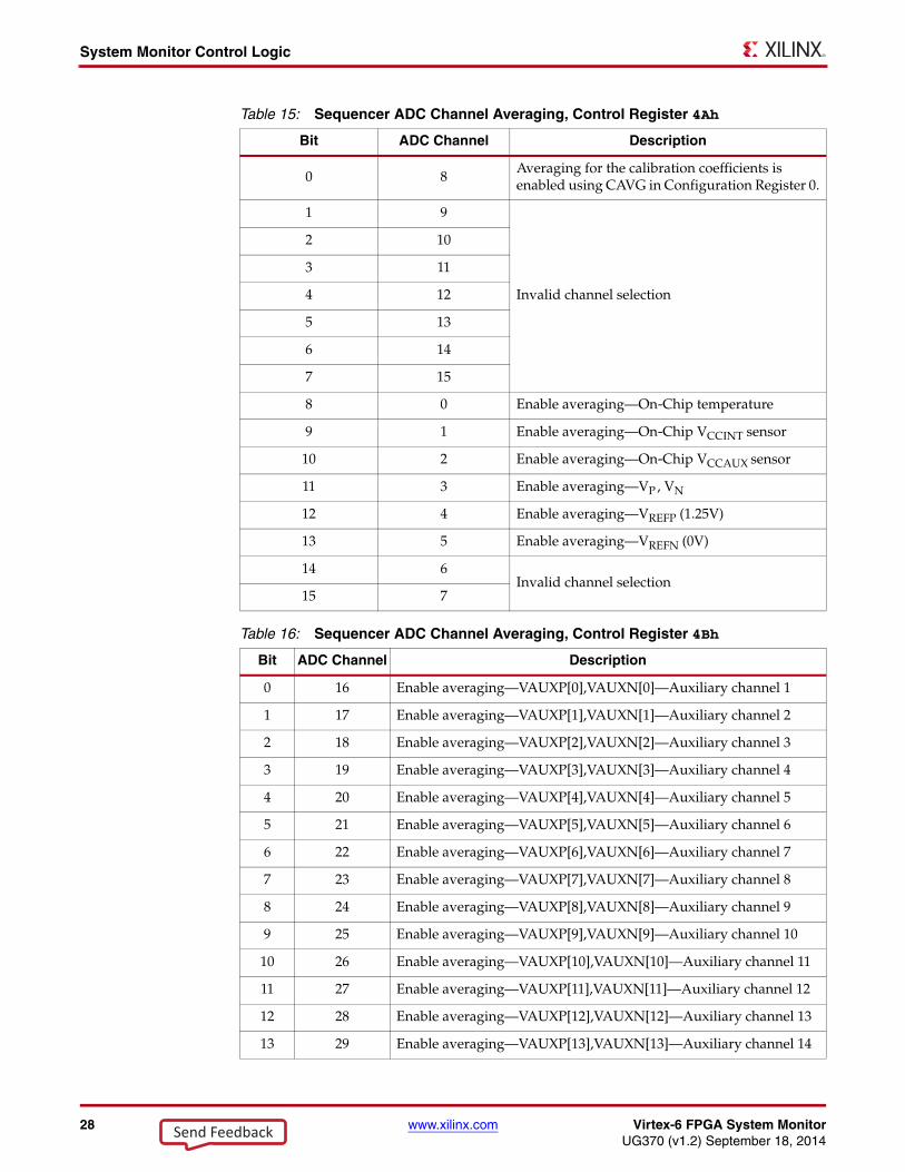
The ADC channel averaging registers enable and disable the averaging of the channel data in the sequence. The result of a measurement on an averaged channel is generated by using 16, 64, or 256 samples. The amount of averaging is selected by using the AVG1 and AVG0 bits in Configuration register 0 (see Configuration Registers (40h to 42h), page 17). Not all channels in the automatic sequence have an averaging feature. The bit definitions for these registers are described in Table 15 and Table 16. Each bit in the two 16-bit registers is used to enable or disable the averaging for its associated channel. A logic 1 enables averaging for a particular channel in the sequence. All channels have the same amount of averaging applied as defined by AVG1 and AVG0 (see Table 8, page 20).
Averaging can be independently selected for each channel in the sequence. When averaging is enabled for some of the channels of the sequence, the EOS will only be pulsed after the sequence has completed the amount of averaging selected by using AVG1 and AVG0. If a channel in the sequence does not have averaging enabled, its status register will be updated for every pass through the sequencer. When a channel has averaging enabled, its status register is only updated after the averaging is complete. An example sequence is Temperature and VAUX[1] and averaging of 16 is enabled on VAUX[1]. The sequence will be Temperature, VAUX[1], Temperature, VAUX[1], ... Temperature, VAUX[1] for each of the conversions where the temperature status register is updated. The VAUX[1] status register is updated after the averaging of the 16 conversions.
If averaging is enabled for the calibration channel (by setting CAVG logic Low), the coefficients will be updated after the first pass through the sequence. Subsequent updates to coefficient registers will require 16 conversions before the coefficients are updated.
12 4 20 VAUXP[4],VAUXN[4]—Auxiliary channel 5
13 5 21 VAUXP[5],VAUXN[5]—Auxiliary channel 6
14 6 22 VAUXP[6],VAUXN[6]—Auxiliary channel 7
15 7 23 VAUXP[7],VAUXN[7]—Auxiliary channel 8
16 8 24 VAUXP[8],VAUXN[8]—Auxiliary channel 9
17 9 25 VAUXP[9],VAUXN[9]—Auxiliary channel 10
18 10 26 VAUXP[10],VAUXN[10]—Auxiliary channel 11
19 11 27 VAUXP[11],VAUXN[11]—Auxiliary channel 12
20 12 28 VAUXP[12],VAUXN[12]—Auxiliary channel 13
21 13 29 VAUXP[13],VAUXN[13]—Auxiliary channel 14
22 14 30 VAUXP[14],VAUXN[14]—Auxiliary channel 15
23 15 31 VAUXP[15],VAUXN[15]—Auxiliary channel 16
Table 14: Sequencer ADC Channel Selection, Control Register 49h (Cont’d)
SequenceNumber
BitADC
ChannelDescription
Send Feedback
28 www.xilinx.com Virtex-6 FPGA System MonitorUG370 (v1.2) September 18, 2014
System Monitor Control Logic
Table 15: Sequencer ADC Channel Averaging, Control Register 4Ah
Bit ADC Channel Description
0 8Averaging for the calibration coefficients is enabled using CAVG in Configuration Register 0.
1 9
Invalid channel selection
2 10
3 11
4 12
5 13
6 14
7 15
8 0 Enable averaging—On-Chip temperature
9 1 Enable averaging—On-Chip VCCINT sensor
10 2 Enable averaging—On-Chip VCCAUX sensor
11 3 Enable averaging—VP , VN
12 4 Enable averaging—VREFP (1.25V)
13 5 Enable averaging—VREFN (0V)
14 6Invalid channel selection
15 7
Table 16: Sequencer ADC Channel Averaging, Control Register 4Bh
Bit ADC Channel Description
0 16 Enable averaging—VAUXP[0],VAUXN[0]—Auxiliary channel 1
1 17 Enable averaging—VAUXP[1],VAUXN[1]—Auxiliary channel 2
2 18 Enable averaging—VAUXP[2],VAUXN[2]—Auxiliary channel 3
3 19 Enable averaging—VAUXP[3],VAUXN[3]—Auxiliary channel 4
4 20 Enable averaging—VAUXP[4],VAUXN[4]—Auxiliary channel 5
5 21 Enable averaging—VAUXP[5],VAUXN[5]—Auxiliary channel 6
6 22 Enable averaging—VAUXP[6],VAUXN[6]—Auxiliary channel 7
7 23 Enable averaging—VAUXP[7],VAUXN[7]—Auxiliary channel 8
8 24 Enable averaging—VAUXP[8],VAUXN[8]—Auxiliary channel 9
9 25 Enable averaging—VAUXP[9],VAUXN[9]—Auxiliary channel 10
10 26 Enable averaging—VAUXP[10],VAUXN[10]—Auxiliary channel 11
11 27 Enable averaging—VAUXP[11],VAUXN[11]—Auxiliary channel 12
12 28 Enable averaging—VAUXP[12],VAUXN[12]—Auxiliary channel 13
13 29 Enable averaging—VAUXP[13],VAUXN[13]—Auxiliary channel 14
Send Feedback
Virtex-6 FPGA System Monitor www.xilinx.com 29UG370 (v1.2) September 18, 2014
System Monitor Control Logic
ADC Channel Analog-Input Mode (4Ch and 4Dh)
These registers are used to configure an ADC channel as either unipolar or bipolar in the automatic sequence (see Analog Inputs, page 39). The registers have the same bit assignments as the Channel Sequence and Channel Averaging registers. However, only external analog-input channels, such as the dedicated-input channels VP, and VN, and the Auxiliary Analog inputs VAUXP[15:0], and VAUXN[15:0]), can be configured in this way. Setting a bit to logic 1 enables a bipolar input mode for the associated channel. Setting a bit to logic 0 (default) enables a unipolar input mode. All internal sensors use a unipolar transfer function.
ADC Channel Acquisition Time (4Eh and 4Fh)
The default acquisition time for an external channel in Continuous-Sampling mode is four ADCCLK cycles. However, by setting the corresponding bits to logic 1 in registers 4Eh and 4Fh, the associated channel can have its acquisition time extended to ten ADCCLK cycles. The bit definitions (which bits correspond to which external channels) for these registers are the same as the Channel Sequence registers described in Table 13 and Table 14. For example, to extend the acquisition time for channel VAUXP[1]/VAUXN[1], bit 1 in register 4Fh is set to a logic 1.
Maximum and Minimum Status RegistersSystem Monitor also tracks the minimum and maximum values recorded for the internal sensors since the last power-up or since the last reset of the System Monitor control logic. The maximum and minimum values recorded are stored in the DRP Status registers starting at address 20h (see Status Registers, page 15). On power-up or after reset, all the minimum registers are set to FFFFh and the maximum registers are set to 0000h. Each new measurement generated for an on-chip sensor is compared to the contents of its maximum and minimum registers. If the measured value is greater than the contents of its maximum registers, then the measured value is written to the maximum register. Similarly, for the minimum register, if the measured value is less than the contents of its minimum register, then the measured value is written to the minimum register. This check is carried out every time a measurement result is written to the status registers.
Automatic AlarmsSystem Monitor also generates an alarm signal on the logic outputs ALM[2:0] when an internal-sensor measurement (Temperature, VCCINT, or VCCAUX) exceeds some user-defined thresholds. Only the values written to the status registers are used to generate alarms. If averaging has been enabled for a sensor channel, then the averaged value is compared to the Alarm Threshold register contents. The alarm outputs are disabled by writing a 1 to bits ALM2, ALM1, and ALM0 in Configuration register 1. The alarm thresholds are stored in Control registers 50h to 57h (see Control Registers, page 17). Table 17 defines the alarm thresholds that are associated with specific Control registers. The limits written to the threshold registers are MSB justified. Limits are derived from the temperature and power-supply sensor transfer functions (see Figure 5, page 13 and Figure 6, page 14).
14 30 Enable averaging—VAUXP[14],VAUXN[14]—Auxiliary channel 15
15 31 Enable averaging—VAUXP[15],VAUXN[15]—Auxiliary channel 16
Table 16: Sequencer ADC Channel Averaging, Control Register 4Bh (Cont’d)
Bit ADC Channel Description
Send Feedback
30 www.xilinx.com Virtex-6 FPGA System MonitorUG370 (v1.2) September 18, 2014
System Monitor Control Logic
Supply Sensor Alarms
When the measured value on the supply sensor for VCCINT or VCCAUX is greater than the thresholds in Control registers 51h and 52h, or less than the thresholds in Control registers 55h and 56h, then the output alarms go active. The alarms are reset when a subsequently measured value falls inside the threshold.
Thermal Management
The on-chip temperature measurement is used for critical temperature warnings. The default Over Temperature threshold is 125°C. This threshold is used for preconfiguration or when the contents of the OT Upper alarm register have not been configured. To override this default condition, the 10 MSBs of the OT Upper register (Control Register 53h) must be set using the temperature sensor transfer function (Figure 5). In addition, the four LSBs must be set to 0011b.
When the die temperature exceeds a factory set limit of 125°C or a user selected threshold, the Over-Temperature alarm logic output (OT) becomes active. This feature can be disabled by the user when System Monitor is instantiated in a design. The OT function is disabled by writing a logic 1 to the OT bit in Configuration register 1. The OT signal resets when the FPGA temperature has fallen below a user-programmable limit in Control register 57h (see Table 17, page 30). When the automatic shut-down feature is enabled, the OT signal can be used to trigger a device shut down. When OT goes active High, the FPGA enters shut down approximately 10 ms later. The shut-down feature initiates a configuration shutdown sequence disabling the device when finished and asserts GHIGH to prevent any contention (see Virtex-6 FPGA Configuration Guide). When OT is deasserted, GHIGH will also deassert and the startup sequence is initiated releasing all global resources. By default this functionality is disabled and must be explicitly enabled. The automatic shut down is enabled by using a configuration option in the ISE™ software, version 9.1i or later. Check the “Power Down Device if Over Safe Temperature” option under “Configuration Options” on the Process Properties GUI for generating a programming file. Alternatively use the bitgen -g command line option OverTempPowerDown:[Enable¦Disable]. When the FPGA enters shut down, System Monitor continues to operate in whatever mode was configured prior to shut down using an internal clock oscillator. The FPGA automatically starts up once the temperature has fallen below the user-programmable lower limit (see Automatic Alarms, page 29). Until the temperature falls below the user-programmable limit, PROGRAM_B has no effect. After the start-up sequence, the device can be reconfigured. The System Monitor OT signal
Table 17: Alarm Threshold Registers (50h to 57h)
Control Register Description Alarm
50h Temperature Upper ALM[0]
51h VCCINT Upper ALM[1]
52h VCCAUX Upper ALM[2]
53h OT Upper OT
54h Temperature Lower ALM[0]
55h VCCINT Lower ALM[1]
56h VCCAUX Lower ALM[2]
57h OT Lower OT
Send Feedback
Virtex-6 FPGA System Monitor www.xilinx.com 31UG370 (v1.2) September 18, 2014
System Monitor Calibration
can also be reset by writing a logic 1 to the OT bit in System Monitor Configuration Register 1 via the JTAG DRP interface. On-chip sensors are monitored via the JTAG TAP during device shut down. During shut down the System Monitor uses an internal oscillator instead of DCLK. On start up, several DCLK cycles will be required to resynchronize the DRP (see System Monitor Timing, page 33).
A second user-programmable temperature threshold level (Control register 50h) is used to carry out a user-defined thermal management procedure, such as powering-on or controlling the speed of a fan. An alarm signal (ALM[0]) becomes active when the FPGA temperature exceeds the limit in this register. The signal is available through the interconnect and is routed using the FPGA resources. The alarm signal resets when the temperature falls below the threshold in Control register 54h. This operation differs for the supply-sensor alarm, because the supply alarm resets when the measurement is between the upper and lower thresholds.
Thermal Diode (DXP and DXN)
Previous generations of Virtex FPGAs allowed users to monitor the die temperature by providing access to a PN junction (diode) on the die. By connecting this diode to an external signal conditioning IC (thermal monitor), the die temperature could be determined. To preserve backward compatibility with these thermal monitoring solutions and to facilitate production test requirements, the thermal diode is also available on Virtex-6 FPGAs. The thermal diode can be accessed by using the DXP and DXN pins in bank 0. The thermal diode is independent of System Monitor, and its use in no way affects the System Monitor operation. If the thermal diode is not being used, these pins should be tied to ground. The thermal diode has a non-ideality factor of ~1.0002 and a series resistance of < 2 Ω . For implementation details, consult the data sheet for the selected external thermal monitoring IC.
System Monitor CalibrationThe Virtex-6 FPGA System Monitor can digitally calibrate out any offset-and-gain errors in the ADC and supply sensor (see Calibration Coefficients for an explanation of offset and gain errors). By connecting known voltages (VREFN and VREFP) to the ADC and supply sensor, the offset-and-gain errors can be calculated and correction coefficients generated. System Monitor has a built-in calibration function that calculates these coefficients automatically. By initiating a conversion on ADC channel 8 (08h), all calibration coefficients are calculated and then applied during normal operation when calibration is enabled. BUSY transitions High for the duration of the entire calibration sequence. This calibration sequence is three times longer than a regular conversion on a sensor channel. These calibration coefficients are applied to measurements by setting the calibration enable bits in Configuration Register 1. See Figure 9, page 18.
Note: Calibration must be enabled to meet the specified performance of the ADC and sensors. Even if the ADC is only being used to monitor external analog inputs, calibration should be enabled.
Send Feedback
32 www.xilinx.com Virtex-6 FPGA System MonitorUG370 (v1.2) September 18, 2014
System Monitor Calibration
Calibration CoefficientsThe calibration coefficients are stored in the status registers at the DRP address locations shown in Table 18..
The offset calibration registers store the offset correction factor for the supply sensor and ADC. The offset correction factor is a 10-bit, two’s complement number and is expressed in LSBs. Similar to other status registers, the 10-bit values are MSB justified in the registers. For example, if the supply sensor has an offset of +5 LSBs (approximately 5 x 3 mV = 15 mV), then the offset coefficient records –5 LSBs or 3FBh, and Status register 08h records 1111 1110 11XX XXXXb.
Note: For the ADC offset, 1 LSB is approximately equal to 1 mV.
The ADC gain calibration coefficient stores the correction factor for any gain error in the ADC. The correction factor is stored in the six LSBs of register 0Ah. These six bits store both sign and magnitude information for the gain correction factor. If the sixth bit is a logic 1, then the correction factor is positive. If it is 0, then the correction factor is negative.
The next five bits store the magnitude of the gain correction factor. Each bit is equivalent to 0.1%. For example., if the ADC has a positive gain error of +1% (see Figure 13, page 33), then the gain calibration coefficient records –1% (the –1% correction applied to cancel the +1% error). Since the correction factor is negative, the sixth bit is set to zero. The remaining magnitude bits record 1%, where 1% = 10 x 0.1% and 10 = 1010 binary. The Status register 0Ah records 0000 0000 0000 1010. With five bits assigned to the magnitude, the calibration can correct errors in the range ± 0.1% x (25 – 1), or ± 3.1%.
Calibration ExampleFigure 13 shows an ADC transfer function containing offset-and-gain errors (red dashed line). The ideal transfer function is shown as a dashed black line. The ADC transfer function has the form of y = m.x + c (linear). Offset is defined as the ADC output code when the input is 0V (where the transfer function crosses the y axis). This offset is removed by digitally subtracting this offset. The result of this offset calibration is shown in Figure 13 by the blue dashed line.
Table 18: Calibration Coefficient Registers
Status Register Coefficient Description
08h Supply Sensor Offset
09h ADC Offset
0Ah ADC Gain Error
Send Feedback

Virtex-6 FPGA System Monitor www.xilinx.com 33UG370 (v1.2) September 18, 2014
System Monitor Timing
The remaining error (deviation from the dashed black line) is caused by gain error or incorrect slope (m). This error is corrected by multiplying the ADC output code by a correction factor.
Note: Digital calibration can result in some loss of the analog input range at the start and end of the ADC input range. This is illustrated in Figure 13 where the ADC output never reaches 3FFh. Typically, the loss of input range is no more than 20 mV at either end of the transfer function. For most monitoring applications, the loss is insignificant.
System Monitor TimingAll System Monitor timing is synchronized to the DCLK. The ADCCLK is equal to DCLK divided by the user selection in configuration register 2 (see Table 11, page 20). The ADCCLK is an internal clock used by the ADC and is not available externally. ADCCLK is only included here to aid in describing the timing.
The ADC block in System Monitor is operated in one of two possible timing modes, continuous-sampling mode and event-driven sampling mode.
• In continuous-sampling mode, the ADC automatically starts a new conversion at the end of a current conversion cycle.
• In event-sampling mode, the user must initiate the next conversion after the current conversion cycle ends, by using the CONVST or CONVSTCLK inputs.
The operating mode is selected by writing to configuration registers 0 (see Configuration Registers (40h to 42h), page 17). A detailed timing diagram for System Monitor is shown in Figure 16, page 38. Table 19, page 39 describes the timing parameters. Reference the Virtex-6 FPGA Data Sheet for the latest System Monitor timing specifications. The robust nature of the System Monitor ensures continued and correct operation even if the external clock input DCLK is stopped. In this situation, the System Monitor automatically switches
X-Ref Target - Figure 13
Figure 13: Offset and Gain Correction
Ideal ADC
Offset andGain Removed
OffsetError
Actual
Positiv
e Gain
Erro
r OffsetRemoved
ADC Code
Input Voltage (VIN)
Code = (Gain x VIN) + Offsety = m.x + c
3FFh
1VUG370_13_060809
Send Feedback
34 www.xilinx.com Virtex-6 FPGA System MonitorUG370 (v1.2) September 18, 2014
System Monitor Timing
over to an internal clock oscillator to continue monitoring. This is similar to the mode of operation pre-configuration (see Pre-Configuration Operation, page 10). After configuration, the DCLK input requires 20 DCLKs to resynchronize to the external clock. It will not be possible to access the DRP until resynchronization has occured.
Continuous SamplingIn continuous-sampling mode, the ADC continues to carry out a conversion on the selected analog inputs. Figure 14 shows the timing associated with continuous-sampling mode. The ADCCLK is generated by a clock divider (see Configuration Registers (40h to 42h), page 17). The analog-to-digital conversion process is divided into two parts, the acquisition phase and the conversion phase.
Acquisition Phase
During the acquisition phase, the ADC acquires the voltage on a selected channel to perform the conversion. The acquisition phase involves charging a capacitor in the ADC to the voltage on the selected channel. The time required to charge this capacitor depends on the selected input-channel source impedance. The acquisition time is nominally four ADCCLKs in duration, from the end of the previous conversion phase to the sampling edge of the next conversion phase (see Figure 14).
When operating in Single Channel mode, the user must write to configuration 0 to select the next channel for conversion. Write operations to the configuration registers to select the next channel should occur before the end of the current conversion (EOC pulse). In sequencer mode, this channel selection is automatically made (see Channel Sequencer Registers (48h to 4Fh), page 21).
If the ACQ bit in configuration register 0 is set to logic 1, then an extra six ADCCLK cycles are inserted before the sampling edge (in Single Channel mode) to allow for more acquisition time on a selected channel. This is useful if an external channel has a large source impedance (greater than 10 kΩ). The extra ADCCLKs are shown in Figure 14 with the additional clock cycles numbered in red. To extend the acquisition time when using the channel sequencer, the desired bits in registers 4Eh and 4F must be set High (see Channel Sequencer, page 25).
For more information on the effects of source impedance on the acquisition, see Analog Input Description.
In Figure 14, ADCCLK is an internal clock used by the ADC.
Send Feedback
Virtex-6 FPGA System Monitor www.xilinx.com 35UG370 (v1.2) September 18, 2014
System Monitor Timing
Conversion Phase
The conversion phase starts on the sampling edge (next rising edge of DCLK) at the end of the acquisition phase. The BUSY signal transitions to an active High on the next rising edge of DCLK to indicate the ADC is carrying out a conversion. The conversion phase is 22 ADCCLK cycles. The conversion result transfers to the status registers 10 DCLK cycles after BUSY transitions Low, and the EOC logic output pulses High for one DCLK cycle. If the channel being converted is also being filtered, then the filtered data is only transferred to the status registers when the last sample result has been converted. Thus, if a channel is being averaged, an EOC pulse is only generated for the last conversion result, such as the 16th, 64th, 256th sample (see ADC Channel Averaging (4Ah and 4Bh), page 27). When averaging is enabled, write operations to the configuration registers will not be acted on until EOC is pulsed, i.e., when the filtering operation is complete.
When System Monitor is being operated in sequence mode, the user identifies the channel being converted by monitoring the channel address (CHANNEL[4:0]) logic outputs. The multiplexer channel address of the channel being converted is updated on these logic outputs when BUSY transitions Low at the end of the conversion phase. The channel address outputs can be used with the EOC and DRDY signals to automatically latch the contents of the output data registers into a FIFO or block RAM (see Example Instantiation of SYSMON, page 49). This is accomplished by connecting the CHANNEL[4:0] outputs to DADDR[4:0] (with DADDR[6:5] = 0), using EOC as a DEN (enable) for the DRP, and using DRDY as a WE (write enable) for the block RAM.
System Monitor’s EOS signal has the same timing as EOC. This signal is pulsed when the output data register for the last channel in a programmed channel sequence is updated.
X-Ref Target - Figure 14
Figure 14: Continuous Sampling Mode Timing
DCLK
1
1041 9 1812 19
2 3 410
612
713
2631
511
2530
1 2 3 432
242329
ADCCLK
Acquisition cycles can be extended to 10 to allow more acquisition time
Acquisition Time Acquisition Time Conversion Time
BUSY Nth Conversion Finished
Nth Sampling EdgeEOC / EOS
ALM[2:0] / OT
CHANNEL[4:0] N-1 Channel Selection N Selection
UG370_14_060809
Send Feedback
36 www.xilinx.com Virtex-6 FPGA System MonitorUG370 (v1.2) September 18, 2014
System Monitor Timing
Event-Driven SamplingFigure 15 illustrates the event-driven sampling mode. In this operation mode, the sampling instant and subsequent conversion process are initiated by a trigger signal called convert start (CONVST). Event-Driven Sampling mode should only be used with external analog inputs when precise control over the sampling instant is necessary. The on-chip sensors and calibration channel should only be monitored in Continuous Sampling mode. It is not possible to use Event-Driven Sampling when the sequencer is enabled.
Note: The DCLK must always be present when using Event-Driven Sampling mode. If no DCLK is present, System Monitor reverts to Continuous mode timing using an internal clock oscillator.
A Low-to-High transition (rising edge) on CONVST or CONVSTCLK defines the exact sampling instant for the selected analog-input channel. The BUSY signal transitions High just after the sampling instant on the next rising edge of DCLK. CONVST can be an asynchronous external signal in which case System Monitor automatically resynchronizes the conversion process to the ADCCLK.
As with the continuous sampling mode, enough time must be allowed for the acquisition phase, that is the time between a channel change and the sampling edge (the rising edge of CONVST or CONVSTCLK, see Analog Input Description). This allows the ADC to acquire the new signal before it is sampled by the CONVST signal and the conversion phase starts. The ACQ bit has no meaning in event-sampling mode because the sampling instant is controlled by CONVST/CONVSTCLK. Therefore the acquisition time on a selected channel is also controlled by the CONVST/CONVSTCLK. CONVST and CONVSTCLK are logically OR'ed within System Monitor.
If a long acquisition time is required, then the user must leave the required acquisition time before CONVST/CONVSTCLK is pulsed. After the analog input has been sampled by a rising edge on CONVST/CONVSTCLK, a conversion is initiated on the next rising edge of ADCCLK. After a conversion has been initiated by CONVST, it is not possible to interrupt the conversion or start a new conversion until BUSY transitions Low. As with continuous mode, the configuration registers should be updated before EOC. To register updates after EOC (for example, switch to continuous mode), a new conversion needs to be initiated by pulsing CONVST.
After BUSY goes Low, the conversion result is transferred to the output status registers ten DCLK cycles later, and the EOC logic output pulses High for one DCLK cycle at this time. If the channel being converted is also being filtered, then the filtered data is only transferred to the status registers when the last sample result has been converted. Thus, if a channel is being filtered, no EOC pulse is generated for all but the last conversion result (such as the 16th, 64th, and 256th sample), depending on the filter setting (see ADC Channel Averaging (4Ah and 4Bh), page 27). An EOC pulse must occur before any new settings written to the configuration registers are acted on. The EOC, EOS, and CHANNEL[4:0] outputs operate in the same way as in the continuous-sampling mode, described previously. If System Monitor is reset while operating in event mode, the first conversion result is valid on an EOC pulse following the first CONVST pulse after RESET is released.
Send Feedback

Virtex-6 FPGA System Monitor www.xilinx.com 37UG370 (v1.2) September 18, 2014
System Monitor Timing
In Figure 15, ADCCLK is an internal clock used by the ADC.X-Ref Target - Figure 15
Figure 15: Event Driven Sampling Mode Timing
EOC / EOS
DCLK
1 84 85 96
1 2 21201918ADCCLK
Acquisition Time Conversion Time
BUSY
CONVST
CHANNEL[4:0] N-1 Channel Selection N Selection
Nth Conversion FinishedNth Sampling Edge
UG370_15_060809
Send Feedback
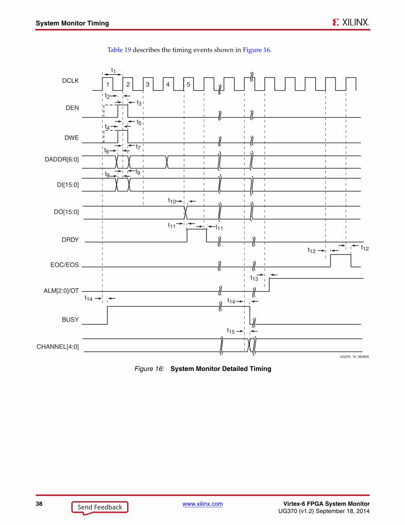
38 www.xilinx.com Virtex-6 FPGA System MonitorUG370 (v1.2) September 18, 2014
System Monitor Timing
Table 19 describes the timing events shown in Figure 16.X-Ref Target - Figure 16
Figure 16: System Monitor Detailed Timing
t5
t9t8
t10
t7t6
t4
t2
t1
t3
DCLK1 2 3 4 5
DWE
DEN
DADDR[6:0]
DI[15:0]
DO[15:0]
DRDY
t11 t11
t13
t14 t14
t15
t12t12
EOC/EOS
ALM[2:0]/OT
BUSY
CHANNEL[4:0]UG370_16_060809
Send Feedback
Virtex-6 FPGA System Monitor www.xilinx.com 39UG370 (v1.2) September 18, 2014
Analog Inputs
Analog InputsThe analog inputs of the ADC use a differential sampling scheme to reduce the effects of common-mode noise signals. This common-mode rejection improves the ADC performance in noisy digital environments. Figure 17 shows the benefits of a differential sampling scheme. Common ground impedances (RG) easily couple noise voltages (switching digital currents) into other parts of a system. These noise signals can be 100 mV or more. For the System Monitor ADC, this noise voltage is equivalent to 100 LSBs, thus inducing large measurement errors. The differential sampling scheme samples both the signal and any common mode noise voltages at both analog inputs (VP and VN). The common mode signal is effectively subtracted because the Track-and-Hold amplifier captures the difference between VP and VN, such as, VP – VN (see Figure 17).
Table 19: Timing Event Information
Event Description
t1 DCLK period(1)
t2 Minimum DEN setup time before the rising edge of DCLK(2)
t3 Minimum DEN hold time after the falling edge of DCLK
t4 Minimum DWE setup time before the rising edge of DCLK(3)
t5 Minimum DWE hold time after the falling edge of DCLK(3)
t6 Minimum DRP address set up time before rising edge of DCLK
t7 Minimum DRP address hold time after rising edge of DCLK
t8 Minimum DRP input data bus set up time before rising edge of DCLK
t9 Minimum DRP input data bus hold time after rising edge of DCLK
t10 Maximum DRP DCLK to DO delay/access time(4)
t11 Maximum delay on DRDY going High/Low after a rising edge on DCLK
t12 Maximum delay on EOC/EOS going High/Low after a rising edge on DCLK
t13 Maximum delay on ALM[2:0]/OT going High after a rising edge on DCLK
t14 Maximum delay on BUSY going High/Low after a rising edge on DCLK
t15 Maximum delay on CHANNEL[4:0] on rising edge of DCLK
Notes: 1. Minimum DCLK duty cycle is 60/40.2. DEN should only be pulsed for one DCLK cycle.3. For a DRP write operation, address on DADDR[6:0] and DI[15:0] are latched on the rising edge of DCLK when DEN and WEN are
High. The data is in placed in the DRP register three DCLK cycles later. DRDY goes High when the data has been written. See the Dynamic Reconfiguration Port description in the Virtex-6 FPGA Configuration Guide for more information.
4. For a DRP read operation, address on DADDR[6:0] is latched on the rising edge of DCLK when DEN is High, and three DCLK cycles later the data is placed on the DO bus. DRDY goes High when the data on DO is valid. See the Dynamic Reconfiguration Port description in the Virtex-6 FPGA Configuration Guide for more information.
Send Feedback

40 www.xilinx.com Virtex-6 FPGA System MonitorUG370 (v1.2) September 18, 2014
Analog Inputs
The dedicated ADC (VP and VN) and auxiliary analog inputs (VAUXP[15:0] and VAUXN[15:0]) can be driven from either unipolar or bipolar sources. When driving the analog inputs from a bipolar source, the inputs must be used in a bipolar mode (see Bipolar Input Signals). Unipolar and bipolar mode selection is made by writing to configuration register 0 (see Configuration Registers (40h to 42h), page 17).
Auxiliary Analog InputsThe auxiliary analog inputs (VAUXP[15:0] and VAUXN[15:0]) are analog inputs shared with regular digital I/O package pins. These analog inputs have a lower input bandwidth than the dedicated analog input channel (VP/VN)
The auxiliary analog input can be enabled as analog inputs preconfiguration only via the JTAG TAP (see JTAG DRP Commands, page 23). To enable all 16 auxiliary analog input channels in preconfiguration operation, a 1 must be written to bit 0 of the register at address 02h (VCCAUX status register) in the System Monitor register file interface. The internal mapping in the System Monitor enables the auxiliary channels using the JTAG interface.
The auxiliary analog inputs are automatically enabled when System Monitor is instantiated in a design, and these inputs are connected in the instantiation. Only the auxiliary inputs connected in a design are enabled as analog inputs. The System Monitor auxiliary input pins are defined in Virtex-6 FPGA Packaging and Pinout Specification as _SMxP_ and _SMxN_, where x is the auxiliary pair number. For example, the auxiliary input VAUXP[15] is designated IO_L10P_CC_SM15P_11 in the pinout specification.
X-Ref Target - Figure 17
Figure 17: Differential Sampling Scheme Rejects Common Mode Noise
NoiseCurrent
T/HVP
VN
Note 1: RG is Common Ground Impedance.
RG(!)
Differential
Common ModeRejection removesnoise
Sampling
0V
1VVP
VN
0V
1VVP – VN
Common Noiseon VP and VN
+
–
UG370_17_060809
NoiseVoltage
Send Feedback
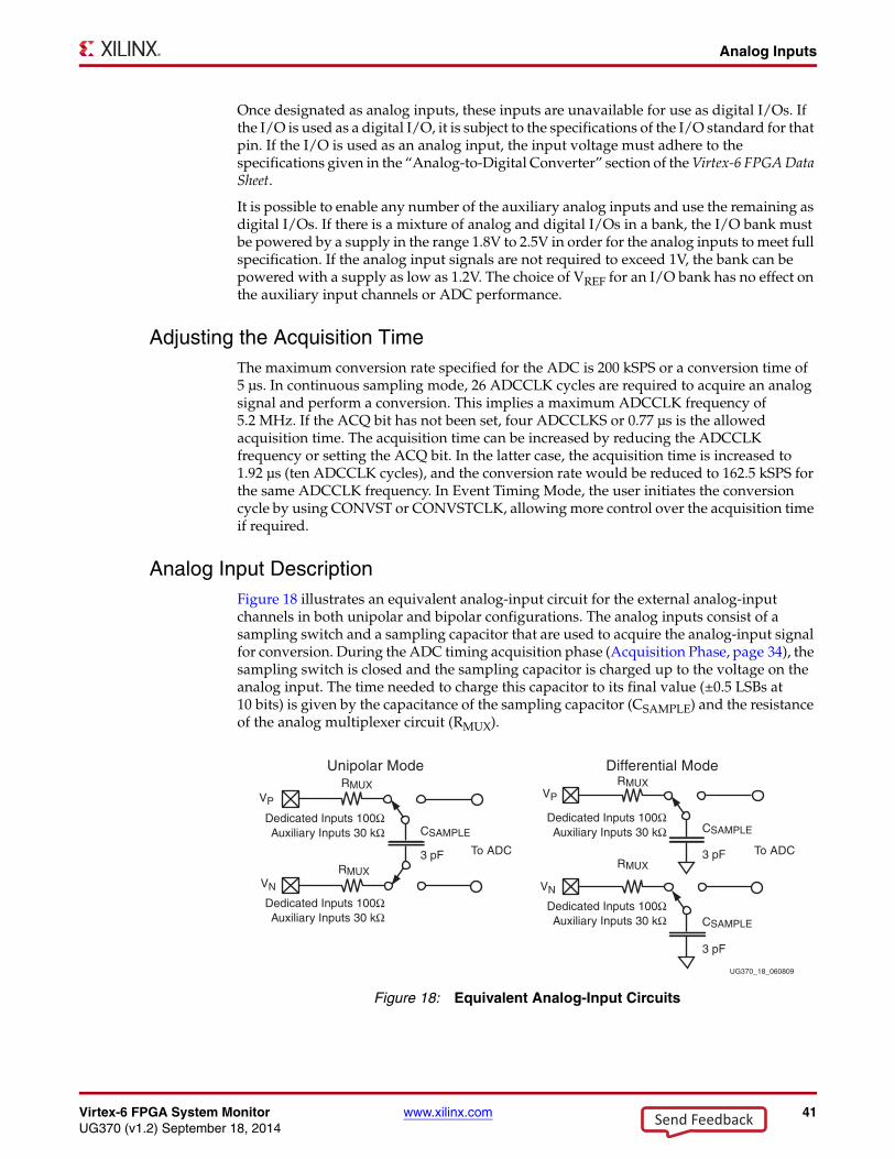
Virtex-6 FPGA System Monitor www.xilinx.com 41UG370 (v1.2) September 18, 2014
Analog Inputs
Once designated as analog inputs, these inputs are unavailable for use as digital I/Os. If the I/O is used as a digital I/O, it is subject to the specifications of the I/O standard for that pin. If the I/O is used as an analog input, the input voltage must adhere to the specifications given in the “Analog-to-Digital Converter” section of the Virtex-6 FPGA Data Sheet.
It is possible to enable any number of the auxiliary analog inputs and use the remaining as digital I/Os. If there is a mixture of analog and digital I/Os in a bank, the I/O bank must be powered by a supply in the range 1.8V to 2.5V in order for the analog inputs to meet full specification. If the analog input signals are not required to exceed 1V, the bank can be powered with a supply as low as 1.2V. The choice of VREF for an I/O bank has no effect on the auxiliary input channels or ADC performance.
Adjusting the Acquisition TimeThe maximum conversion rate specified for the ADC is 200 kSPS or a conversion time of 5 µs. In continuous sampling mode, 26 ADCCLK cycles are required to acquire an analog signal and perform a conversion. This implies a maximum ADCCLK frequency of 5.2 MHz. If the ACQ bit has not been set, four ADCCLKS or 0.77 µs is the allowed acquisition time. The acquisition time can be increased by reducing the ADCCLK frequency or setting the ACQ bit. In the latter case, the acquisition time is increased to 1.92 µs (ten ADCCLK cycles), and the conversion rate would be reduced to 162.5 kSPS for the same ADCCLK frequency. In Event Timing Mode, the user initiates the conversion cycle by using CONVST or CONVSTCLK, allowing more control over the acquisition time if required.
Analog Input DescriptionFigure 18 illustrates an equivalent analog-input circuit for the external analog-input channels in both unipolar and bipolar configurations. The analog inputs consist of a sampling switch and a sampling capacitor that are used to acquire the analog-input signal for conversion. During the ADC timing acquisition phase (Acquisition Phase, page 34), the sampling switch is closed and the sampling capacitor is charged up to the voltage on the analog input. The time needed to charge this capacitor to its final value (±0.5 LSBs at 10 bits) is given by the capacitance of the sampling capacitor (CSAMPLE) and the resistance of the analog multiplexer circuit (RMUX).X-Ref Target - Figure 18
Figure 18: Equivalent Analog-Input Circuits
To ADC
Unipolar Mode
3 pF
RMUXVP
VN
Dedicated Inputs 100ΩAuxiliary Inputs 30 kΩ
Dedicated Inputs 100ΩAuxiliary Inputs 30 kΩ
UG370_18_060809
RMUX
CSAMPLE
Differential Mode
VP
VN
Dedicated Inputs 100ΩAuxiliary Inputs 30 kΩ
Dedicated Inputs 100ΩAuxiliary Inputs 30 kΩ
To ADC3 pF
CSAMPLE
3 pF
RMUX
RMUX
CSAMPLE
Send Feedback
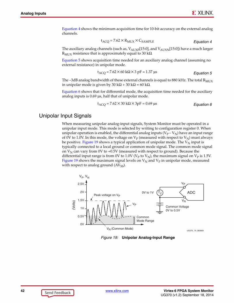
42 www.xilinx.com Virtex-6 FPGA System MonitorUG370 (v1.2) September 18, 2014
Analog Inputs
Equation 4 shows the minimum acquisition time for 10-bit accuracy on the external analog channels.
Equation 4
The auxiliary analog channels (such as, VAUXP[15:0], and VAUXN[15:0]) have a much larger RMUX resistance that is approximately equal to 30 kΩ.
Equation 5 shows acquisition time needed for an auxiliary analog channel (assuming no external resistance) in unipolar mode.
Equation 5
The –3dB analog bandwidth of these external channels is equal to 880 kHz. The total RMUX in unipolar mode is given by 30 kΩ + 30 kΩ = 60 kΩ.
Equation 6 shows that for differential mode, the acquisition time needed for the auxiliary analog inputs is 0.69 µs, half that of unipolar mode.
Equation 6
Unipolar Input SignalsWhen measuring unipolar analog-input signals, System Monitor must be operated in a unipolar input mode. This mode is selected by writing to configuration register 0. When unipolar operation is enabled, the differential analog inputs (VP – VN) have an input range of 0V to 1.0V. In this mode, the voltage on VP (measured with respect to VN) must always be positive. Figure 19 shows a typical application of unipolar mode. The VN input is typically connected to a local ground or common mode signal. The common mode signal on VN can vary from 0V to +0.5V (measured with respect to ground). Because the differential input range is from 0V to 1.0V (VP to VN), the maximum signal on VP is 1.5V. Figure 19 shows the maximum signal levels on VN and VP in unipolar mode, measured with respect to analog ground (AVSS).
tACQ = 7.62 × RMUX × CSAMPLE
tACQ = 7.62 × 60 kΩ × 3 pF = 1.37 µs
tACQ = 7.62 × 30 kΩ × 3pF = 0.69 µs
X-Ref Target - Figure 19
Figure 19: Unipolar Analog-Input Range
VP, VN
(Vol
ts)
0V
0.5V
1.5V
2.5V
1V
2V
CommonMode Range
Peak voltage on VP
VN (Common Mode)
VP
VP
VN
Common Voltage0V to 0.5V
0V to 1V ADC
UG370_19_060809
Send Feedback
Virtex-6 FPGA System Monitor www.xilinx.com 43UG370 (v1.2) September 18, 2014
Analog Inputs
The ADC output coding in unipolar mode is straight binary. The designed code transitions occur at successive integer LSB values such as 1 LSB, 2 LSBs, and 3 LSBs (and so on). The LSB size in volts is equal to 1V/210 or 1V/1024 = 0.977 mV. The ideal transfer function is illustrated in Figure 20.
Bipolar Input SignalsThe analog inputs can accomodate analog input signals which are positive and negative with respect to a common mode or reference. To accomodate these types of signals, the ADC must be operated in bipolar mode. Bipolar mode is selected by writing to configuration register 0. All input voltages must be positive with respect to analog ground (AVSS).
When bipolar operation is enabled, the differential analog input (VP – VN) can have a maximum input range of ±0.5V. The common mode or reference voltage should not exceed 0.5V in this case (see Figure 21). At a maximum common mode voltage of 1V on VN the differential analog input (VP – VN) should not exceed ±100 mV.
X-Ref Target - Figure 20
Figure 20: Unipolar Transfer Function
Input Voltage (mV)
10-B
it O
utpu
t Cod
e (H
ex)
UG370_20_060809
000
001
003
004
3FF
Output CodeFull ScaleTransition
3FE
3FD
002
1 2 3 999
Full Scale Input = 1V1 LSB = 1V / 1024 = 977 µV
X-Ref Target - Figure 21
Figure 21: Differential Analog-Input Range
UG370_21_060809
VP, VN
Vol
ts
0V
0.5V
1.5V
2.5V
1V
2V
VP
VN
±0.5V – ±0.1V
0.5V – 1V
ADC
VP= ±0.5V
VP= ±0.1V
VN = 0.5V
VN = 1V
Send Feedback

44 www.xilinx.com Virtex-6 FPGA System MonitorUG370 (v1.2) September 18, 2014
Analog Inputs
The bipolar input mode also accommodates inputs signals driven from a true differential source for example, a balanced bridge. In this case, VN and VP can swing positive and negative relative to a common mode or reference voltage (see Figure 22). The maximum differential input (VP – VN) is ±0.5V. With maximum differential input voltages of ±0.5V and assuming balanced inputs on VN and VP,the common mode voltage must lie in the range 0.25V to 0.75V.
The output coding of the ADC in bipolar mode is two’s complement and is intended to indicate the sign of the input signal on VP relative to VN. The designed code transitions occur at successive integer LSB values that is, 1 LSB, 2 LSBs, 3 LSBs etc. The LSB size in volts is equal to 1V/210 or 1V/1024 = 0.977 mV. The ideal transfer function is illustrated in Figure 23.
X-Ref Target - Figure 22
Figure 22: Bipolar Signals
X-Ref Target - Figure 23
Figure 23: Bipolar Transfer Function
UG370_22_060809
VP
VCM = (VP + VN) / 2
VP, VN
Vol
ts
VN
0V
0.5V
1.5V
2.5V
1V
2V Common Mode Range0.25V to 0.75V
VP
VN
CommonVoltage0.25V to 0.75V
±0.25V+
+
±0.25V
ADC
Output Code(Two’s Complement
Coding)
-3 +1 +20-2 -1 +499-500
Full Scale Input = 1V1 LSB = 1V / 1024 = 0.977 µV
200h
201h
000h
001h
002h
1FEh
1FFh
3FFh
3FEh
3FDh10-B
it O
utpu
t Cod
e
Input Voltage (mV)UG370_23_060809
Send Feedback
Virtex-6 FPGA System Monitor www.xilinx.com 45UG370 (v1.2) September 18, 2014
Application Guidelines
Application GuidelinesThe Virtex-6 FPGA System Monitor is a precision analog measurement system based on a 10-bit Analog-to-Digital Converter (ADC) with an LSB size that is approximately equal to 1 mV. To achieve the best possible performance and accuracy with all measurements (both on-chip and external), a number of dedicated pins for the ADC reference and power supply are provided. Care must be taken with the connection of these pins to ensure the best possible performance from the ADC. Basic design guidelines to be considered as part of the requirements for board design are outlined in this section. Finally, an instantiation of a basic System Monitor in a design is discussed.
Reference Inputs (VREFP and VREFN)These high-impedance inputs are used to deliver a differential-reference voltage for the analog-to-digital conversion process. ADCs are only as accurate as the reference provided. Any reference-voltage error results in a gain error vs. the ideal ADC transfer function (Figure 20, page 43). Errors in the reference voltage affect the accuracy of absolute measurements for both on-chip sensors and external channels.
For typical usage, the reference voltage between VREFP and VREFN should be maintained at 1.25V ± 0.2% using an external reference IC. Reference voltage ICs that deliver 1.25V are widely available from several vendors. Many vendors offer reference voltage ICs in small packages (SOT-23 and SC70). The 1.25V reference should be placed as close as possible and connected directly to the VREFP input, using the decoupling capacitors recommended in the reference IC data sheet. The recommended reference connections are illustrated in Figure 24.
The System Monitor also has an on-chip reference which is selected by connecting VREFP and VREFN to AGND as shown in Figure 24. Due to reduced accuracy, the on-chip reference does impact the measurement performance of the System Monitor as explained in this section. The performance with on-chip reference is specified in the Virtex-6 FPGA Data Sheet.
Analog Power Supply and Ground (AVDD and AVSS)These inputs provide the power supply and ground reference for the analog circuitry (such as the ADC) in System Monitor.
A common mechanism for the coupling of noise into an analog circuit is from the power supply and ground connections. Excessive noise on the analog supply or ground reference affects the ADC measurement accuracy. For example, I/O switching activity can cause significant disturbance of the digital ground reference plane.
Thus, it would not be advisable to use the digital ground as an analog ground reference for System Monitor.
Similarly, for the digital supplies for the FPGA logic, high switching rates easily result in high-frequency voltage variations on the supply, even with decoupling. In an effort to mitigate these effects on the ADC performance, a dedicated supply and ground reference is provided. Figure 24 illustrates how to use the 2.5V VCCAUX supply to power the analog circuitry. VCCAUX is filtered using a low-pass network. The filter design depends on the ripple and ripple frequency (if any) on the VCCAUX supply. There is also a power-supply region specification for the external reference circuit. The filtering should ensure no more than 2–3 mV of noise on the reference output to minimize any impact on ADC accuracy.
Send Feedback

46 www.xilinx.com Virtex-6 FPGA System MonitorUG370 (v1.2) September 18, 2014
Application Guidelines
The other source of noise coupling into the ADC is from the ground reference AVSS. In mixed-signal designs, it is common practice to use a separate analog ground plane for analog circuits to isolate the analog and digital ground return paths to the supply. Common ground impedance is a mechanism for noise coupling and needs to be carefully considered when designing the PCB. This is shown in Figure 17, page 40, where the common ground impedance RG converts digital switching currents into a noise voltage for the analog circuitry. However, it is often not possible or practical to implement a separate analog ground plane in a design. One solution is to isolate VREFN and AVSS, ground references (such as a trace) from the digital ground (plane) using a ferrite bead (Figure 24).
The ferrite bead behaves like a resistor at high frequencies and functions as a lossy inductor. A typical ferrite impedance vs. frequency plot is shown in Figure 25. The ferrite helps provide high frequency isolation between digital and analog grounds. The reference IC maintains a 1.25V difference of between VREFP and VREFN. The ferrite offers little resistance to the analog DC return current.
X-Ref Target - Figure 24
Figure 24: System Monitor ADC Power and Ground Connections
ADC
2.5V ±5%
~ 12 mA
~ 12 mA
10 nF
470 nF
VCCAUX
10 nF
AVDD
AVSS
VREFP
VREFN
DigitalGroundReference
Analog Ground Trace
Ferrite beads providehigh frequency isolation
External Reference
~ 50 µA
~ 50 µA
REF3012REF3112MAX6018
Filter VCCAUX supply
ADC
2.5V ±5%
~ 12 mA
~ 12 mA
470 nF
VCCAUX
10 nF
AVDD
AVSS
VREFP
VREFN
Ferrite beads providehigh frequency isolation
On-Chip Reference
UG370_24_042910
Filter VCCAUX supply
X-Ref Target - Figure 25
Figure 25: Ferrite Impedance Versus Frequency Plot
Impe
danc
e (Ω
)
UG370_25_060809Frequency (MHz)
Z , R, and XL vs Frequency
XL
R
Z
Z
R
XL
200
400
600
800
1000
1200
0100101 1000 10000
Send Feedback

Virtex-6 FPGA System Monitor www.xilinx.com 47UG370 (v1.2) September 18, 2014
Application Guidelines
The reference inputs should be routed as a tightly coupled differential pair from the reference IC to the package pins. If routed on the same signal layer, the supply and analog ground traces (AVDD and AVSS) should be used to shield the reference inputs because they have a higher tolerance to any coupled noise.
External Analog InputsThe analog inputs are high-impedance differential inputs. The differential input scheme enables the rejection on common mode noise on any externally applied analog-input signal. Because of the high impedance of each input (such as VP and VN), the input AC impedance is typically determined by the sensor, the output impedance of the driving circuitry, or other external components. Figure 26 illustrates a simple example where a simple resistor divider network is used to monitor an external 2.5V supply rail in unipolar input mode (see Figure 18, page 41). To ensure that noise coupled onto the analog inputs is common to both inputs (reduce differential noise), the impedance on each input should be matched. Analog-input traces on the PCB should also be routed as tightly coupled differential pairs.
Anti-Alias Filters
Also shown in Figure 26, is a low-pass filter network at the analog differential inputs. This filter network is commonly referred to as the anti-alias filter and should be placed as close as possible to the package pins. The sensor can be placed remotely from the package as long as the differential input traces are closely coupled. The anti-alias filter attenuates high frequency signal components entering the ADC where they could be sampled and aliased, resulting in ADC measurement corruption. A discussion of aliasing in sampled systems is beyond the scope of this document. A good data-converter reference book provides more information on this topic.
PC Board Design GuidelinesFigure 27 and Figure 28 illustrate one possible way to address the requirements outlined in the previous sections. Figure 27 shows how, by staggering the vias with respect to the pads, north-south and east-west routing channels through the via field are created. These routing channels can be used to bring tightly coupled differential pairs into the center of the via field—even when using 5 mil tolerances.
X-Ref Target - Figure 26
Figure 26: Voltage Attenuation Example
0.5V10 nF
1 k
1 k
VAUXP[x]
VAUXN[x]
Place Anti-Alias FiltersClose to Package Pins
Tightly Coupled Routing(long traces) for VAUXP and VAUXN
+2.5V
5 k
4 k
20 k
UG370_26_060809
Send Feedback
48 www.xilinx.com Virtex-6 FPGA System MonitorUG370 (v1.2) September 18, 2014
Application Guidelines
In Figure 28, the pads have been removed for clarity. The reference inputs (VREFP and VREFN) are routed as a tightly coupled differential pair from an external 1.25V reference IC at the bottom edge of the FPGA (refer to Figure 24, page 46 for the connections). The
X-Ref Target - Figure 27
Figure 27: Routing Channels to Center of Array Created by Staggering Vias
X-Ref Target - Figure 28
Figure 28: Reference Inputs (VREFP and VREFN) should be Routed as Differential Pairs into the Center of the BGA
UG370_27_060809
UG370_28_060809
Send Feedback
Virtex-6 FPGA System Monitor www.xilinx.com 49UG370 (v1.2) September 18, 2014
Application Guidelines
analog power supply and ground reference are also routed into the center of the BGA using traces. No power planes are required to supply a ground reference for System Monitor. The analog supply and ground reference are connected to the external reference IC as shown in Figure 24, page 46. In the PCB implementation shown in Figure 28, the supply and ground traces are routed on either side of the reference traces on the same signal layer and act as guards between the reference traces and any potential aggressors (e.g., clocks and switching I/Os). It is not a requirement that the supply and ground traces are routed on the same signal layer as shown, but they should be routed on an adjacent layer. The VREFN and AVSS traces should be connected at (or close to) the ground pin of the reference IC. The ferrite bead that connects the analog ground trace to system ground should also be placed close to the reference IC. Also shown in Figure 28 is the routing (from the top) of the dedicated analog input pair (VP and VN). These inputs are also routed as a differential pair.
The external reference IC should be placed as close as possible to the FPGA to reduce the opportunities for coupled noise and to minimize any impedances in the reference traces. The staggered via field also allows the 10 nF decoupling on VREFP and AVDD to be placed in the center of the array close to the package balls. VREFP should be decoupled to VREFN and AVDD to AVSS near the package balls.
When using the on-chip reference, the layout of the PCB is greatly simplified. The VREFP and VREFN pins should be shorted to AGND locally at the package balls - see Figure 24, page 46. The ferrite beads used to separate AGND and digital GND should be placed close to the System Monitor balls in the center of the array along with a 10 nF decoupling capacitor for AVDD.
Figure 27 and Figure 28 are only intended to guide a PC board implementation. If it is feasible to create an analog reference plane, then there is no issue with doing this. However, the reference inputs should still be routed as differential pairs as shown.
Example Instantiation of SYSMONThe following sample design is intended to illustrate a basic instantiation of the Virtex-6 FPGA System Monitor in a design (refer to System Monitor Primitive, page 8 for details on the System Monitor I/O and attributes). Figure 29 illustrates a block diagram of the sample design. In this design, SYSMON is set up to monitor the VCCAUX supply and generate an alarm on ALM[2], if the monitored supply moves outside the specified limits. The measured value of VCCAUX can be checked at any time on the DO bus. The design requires an external clock to be provided. This design uses a 50 MHz external clock.
Note: Because an internal clock divider is provided, a clock in the range 2 MHz to 200 MHz can be used as a clock source.
The BUSY signal is also brought out so the ADC conversion rate is easily monitored. The BUSY signal is also used to clock the DO data into a logic analyzer or other data acquisition system for inspection. By varying the VCCAUX supply on the board, the alarm can be triggered or the varying supply voltage can be monitored on the DO bus.
Send Feedback
50 www.xilinx.com Virtex-6 FPGA System MonitorUG370 (v1.2) September 18, 2014
Application Guidelines
SYSMON I/O
For this design the SYSMON I/Os listed in Table 20 are used.
X-Ref Target - Figure 29
Figure 29: System Monitor Sample Design
DO[15:6]
DADDR[4:0]
DWE
RESET
DEN
CHANNEL[4:0]
DCLK
50 MHzExternal Clock
ALM[2]
EOS
BUSY
SYSMON
DADDR[5]
DADDR[6]
0
0
0
0
clk
busy
alarm
VCCAUX[9:0]
10-Bit VCCAUX Measurement (3 mV / LSB)
UG370_29_060809
Table 20: SYSMON I/Os
Name I/O Description
DADDR[6:0] Inputs DRP address bus. The status registers (for example, measurement results) are accessed via the DRP. In this sample design, the CHANNEL[4:0] bus is connected to DADDR[4:0] and DADDR[6:5] are connected to logic 0.
DEN Input DRP enable signal. When High, the address on DADDR[6:0] is latched, and the contents of the corresponding register is placed on the DO[15:0] bus. In this example, DEN is connect to EOS.
DWE Input DRP write enable. Since no writes take place to the DRP, this input is held at logic 0.
RESET Input SYSMON reset signal. It is tied to logic 0 in this example.
CHANNEL[4:0] Output ADC input multiplexer address. The ADC input multiplexer address is placed on this bus at the end of the conversion when BUSY transitions Low (refer to System Monitor Timing, page 33). Because the results of input MUX address 02h (VCCAUX) are placed in the status register at DRP address 02h, these outputs can be used to drive the DADDR[6:0] inputs to access the VCCAUX result.
EOS Output End-of-Sequence output. EOS pulses High for one DCLK cycle at the end of a full channel sequence. In this example, VCCAUX is the last channel in the sequence, allowing EOS to be used as an input to DEN to latch the address on DADDR[6:0] and enable the contents of Status register 02h onto the DO bus for reading.
Send Feedback
Virtex-6 FPGA System Monitor www.xilinx.com 51UG370 (v1.2) September 18, 2014
Application Guidelines
SYSMON Attributes
In the example, System Monitor is set up in an automatic channel sequence mode that includes the Calibration Channel and VCCAUX Channel. Averaging is enabled for the VCCAUX channel. Sixteen ADC conversion results on VCCAUX are used to generate the averaged measurement. The lower and upper alarm thresholds for VCCAUX are 2.375V and 2.625V respectively. The target conversion rate for the ADC is 200 kSPS (200 kHz).
DO[15:0] Output DRP data output bus. The result of the ADC conversion on the VCCAUX channel is placed on this bus shortly after EOS pulses High (when DRDY does high). Refer to System Monitor Timing for more information.
BUSY Output System Monitor busy. This logic signal goes High for the duration of the ADC conversion. The rising edge can be used to latch the DO bus data into an external acquisition system, for example, a logic analyzer. BUSY also toggles at the conversion frequency of the ADC. In this example, the conversion rate is set to 192.3 kHz (refer to SYSMON Attributes).
ALM[2] Output VCCAUX supply measurement alarm. The Alarm limits are set to 2.5 ± 5% in this example (2.375V and 2.625V). When the supply moves outside these limits, ALM[2] goes active High. The output resets to Low again after the measured VCCAUX supply is inside the limits.
Table 20: SYSMON I/Os (Cont’d)
Name I/O Description
Table 21: SYSMON Attributes
Attribute Setting Description
INIT_40 1000h Set averaging to 16 (AVG1 = 0 & AVG0 = 1). Refer to Figure 9, page 18 and Table 6, page 18.
INIT_41 20C7h Enable Auto Channel Sequence Mode (SEQ1 = 1 & SEQ0 = 0). Enable Offset and Gain calibration on the Supply Sensor (CAL3 = 1 & CAL2 = 1). Enable VCCAUX Alarm (ALM[2]) by setting ALM2 to 0. All other alarm bits are set to 1 to disable. See Figure 9 and Table 6 for more information.
INIT_42 0A00h DCLK frequency is 50 MHz. Desired ADC conversion rate is 200 kSPS and requires 26 ADCCLK cycles to perform one ADC conversion. CD = 50 MHz/(26 x 200 kHz) = 9.6. Only integers allowed set CD7 to CD0 (ADCCLK divider) to 10 (0Ah). Actual ADC conversion rate is 192.3 kHz. Refer to Figure 9 and Table 6 for more information.
INIT_48 0401h Select Calibration and VCCAUX Channel for the Sequencer (refer to ADC Channel Selection (48h and 49h), page 26.
INIT_49 0000h
INIT_4A 0400h Enable Averaging on the VCCAUX channel (refer to ADC Channel Averaging (4Ah and 4Bh), page 27.
INIT_4B 0000h
Send Feedback
52 www.xilinx.com Virtex-6 FPGA System MonitorUG370 (v1.2) September 18, 2014
Application Guidelines
INIT_4C 0000h Analog input mode does not apply and is not used (refer to ADC Channel Selection (48h and 49h)).
INIT_4D 0000h
INIT_4E 0000h Acquisition Time is not used (refer to ADC Channel Acquisition Time (4Eh and 4Fh)).
INIT_4F 0000h
INIT_52 E000h The upper alarm threshold for VCCAUX is generated from the transfer function for the power supply sensor, as shown in Figure 6, page 14. The limit can be calculated as (Limit/3V) * 216. Therefore, (2.625/3) * 216 = 57344 or E000h. The value of the top 10 bits is 380h (refer to Figure 6).
INIT_56 CAAAh The lower alarm threshold for VCCAUX is also generated from the transfer function for the power supply sensor, as shown in Figure 6. The limit can be calculated as (Limit/3V) * 216. Therefore (2.375/3) * 216 = 51882 or CAAAh.
Table 21: SYSMON Attributes (Cont’d)
Attribute Setting Description
Send Feedback
Virtex-6 FPGA System Monitor www.xilinx.com 53UG370 (v1.2) September 18, 2014
Application Guidelines
Example Instantiation using Verilog
Below is an example of how this design is instantiated. This design can be instantiated in any Virtex-6 device as a stand-alone design. Only an external clock is required to access the data on the DO bus.
Note: If the DCLK is not present or disconnected, SYSMON switches over to an internal clock oscillator and continues to monitor VCCAUX. In this situation, data is not updated on the DO bus because a DCLK is needed to access the DRP. The ALARM and BUSY signal remains active however. The result in status register 2 (VCCAUX) can be accessed via the JTAG TAP (refer to DRP JTAG Interface, page 21).
//////////////////////////////////////////////////////////////////////////// Author: Xilinx// Date: July 11th 2007 $// Design: Virtex-6 FPGA System Monitor Verilog example instantiation //// System Monitor instantiation by hand using the Language Template// ////////////////////////////////////////////////////////////////////////
`timescale 1ns / 1 ps
module v5_sysmon (
// Inputs clk, // Outputs Vccaux, busy, alarm ); //Inputs input clk; //Output output [9:0] Vccaux; output busy; output alarm; wire [15:0] dobus; wire [4:0] channel; wire [2:0] alm; wire eos;
// bring out 10-bit (MSBs) version of DO bus assign Vccaux = dobus[15:6]; assign alarm = alm[2];
// SYSMON: System Monitor// Virtex-6 // Xilinx HDL Language Template, version 9.2.1i
Send Feedback
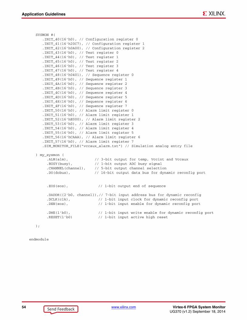
54 www.xilinx.com Virtex-6 FPGA System MonitorUG370 (v1.2) September 18, 2014
Application Guidelines
SYSMON #( .INIT_40(16'h0), // Configuration register 0 .INIT_41(16'h20C7), // Configuration register 1 .INIT_42(16'h0A00), // Configuration register 2 .INIT_43(16'h0), // Test register 0 .INIT_44(16'h0), // Test register 1 .INIT_45(16'h0), // Test register 2 .INIT_46(16'h0), // Test register 3 .INIT_47(16'h0), // Test register 4 .INIT_48(16'h0401), // Sequence register 0 .INIT_49(16'h0), // Sequence register 1 .INIT_4A(16'h0), // Sequence register 2 .INIT_4B(16'h0), // Sequence register 3 .INIT_4C(16'h0), // Sequence register 4 .INIT_4D(16'h0), // Sequence register 5 .INIT_4E(16'h0), // Sequence register 6 .INIT_4F(16'h0), // Sequence register 7 .INIT_50(16'h0), // Alarm limit register 0 .INIT_51(16'h0), // Alarm limit register 1 .INIT_52(16'hE000), // Alarm limit register 2 .INIT_53(16'h0), // Alarm limit register 3 .INIT_54(16'h0), // Alarm limit register 4 .INIT_55(16'h0), // Alarm limit register 5 .INIT_56(16'hCAAA), // Alarm limit register 6 .INIT_57(16'h0), // Alarm limit register 7 .SIM_MONITOR_FILE("vccaux_alarm.txt") // Simulation analog entry file
) my_sysmon ( .ALM(alm), // 3-bit output for temp, Vccint and Vccaux .BUSY(busy), // 1-bit output ADC busy signal .CHANNEL(channel), // 5-bit output channel selection .DO(dobus), // 16-bit output data bus for dynamic reconfig port .EOS(eos), // 1-bit output end of sequence .DADDR({2'b0, channel}),// 7-bit input address bus for dynamic reconfig .DCLK(clk), // 1-bit input clock for dynamic reconfig port .DEN(eos), // 1-bit input enable for dynamic reconfig port .DWE(1'b0), // 1-bit input write enable for dynamic reconfig port .RESET(1'b0) // 1-bit input active high reset );
endmodule
Send Feedback
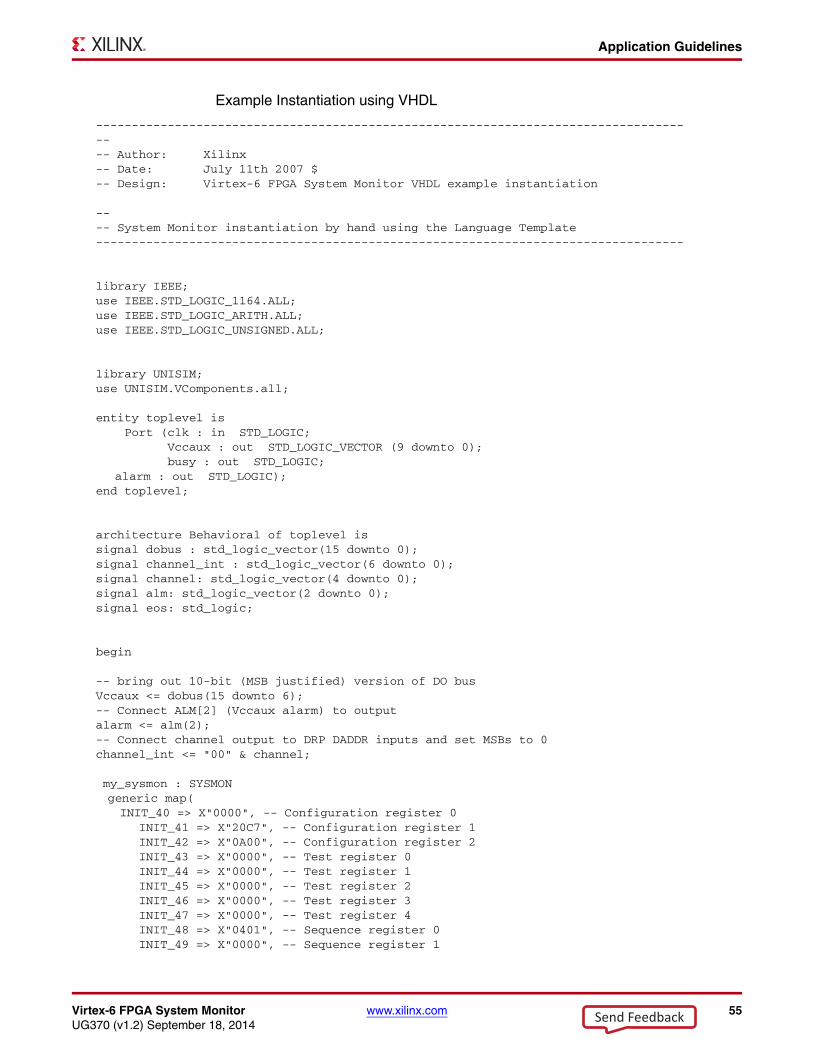
Virtex-6 FPGA System Monitor www.xilinx.com 55UG370 (v1.2) September 18, 2014
Application Guidelines
Example Instantiation using VHDL
-------------------------------------------------------------------------------------- Author: Xilinx-- Date: July 11th 2007 $-- Design: Virtex-6 FPGA System Monitor VHDL example instantiation
-- -- System Monitor instantiation by hand using the Language Template----------------------------------------------------------------------------------
library IEEE;use IEEE.STD_LOGIC_1164.ALL;use IEEE.STD_LOGIC_ARITH.ALL;use IEEE.STD_LOGIC_UNSIGNED.ALL;
library UNISIM;use UNISIM.VComponents.all;
entity toplevel is Port (clk : in STD_LOGIC; Vccaux : out STD_LOGIC_VECTOR (9 downto 0); busy : out STD_LOGIC; alarm : out STD_LOGIC);
end toplevel;
architecture Behavioral of toplevel issignal dobus : std_logic_vector(15 downto 0);signal channel_int : std_logic_vector(6 downto 0);signal channel: std_logic_vector(4 downto 0);signal alm: std_logic_vector(2 downto 0);signal eos: std_logic;
begin
-- bring out 10-bit (MSB justified) version of DO busVccaux <= dobus(15 downto 6);-- Connect ALM[2] (Vccaux alarm) to outputalarm <= alm(2);-- Connect channel output to DRP DADDR inputs and set MSBs to 0channel_int <= "00" & channel;
my_sysmon : SYSMON generic map(
INIT_40 => X"0000", -- Configuration register 0 INIT_41 => X"20C7", -- Configuration register 1 INIT_42 => X"0A00", -- Configuration register 2 INIT_43 => X"0000", -- Test register 0 INIT_44 => X"0000", -- Test register 1 INIT_45 => X"0000", -- Test register 2 INIT_46 => X"0000", -- Test register 3 INIT_47 => X"0000", -- Test register 4 INIT_48 => X"0401", -- Sequence register 0 INIT_49 => X"0000", -- Sequence register 1
Send Feedback

56 www.xilinx.com Virtex-6 FPGA System MonitorUG370 (v1.2) September 18, 2014
Application Guidelines
INIT_4A => X"0000", -- Sequence register 2 INIT_4B => X"0000", -- Sequence register 3 INIT_4C => X"0000", -- Sequence register 4 INIT_4D => X"0000", -- Sequence register 5 INIT_4E => X"0000", -- Sequence register 6 INIT_4F => X"0000", -- Sequence register 7 INIT_50 => X"0000", -- Alarm limit register 0 INIT_51 => X"0000", -- Alarm limit register 1 INIT_52 => X"E000", -- Alarm limit register 2 INIT_53 => X"0000", -- Alarm limit register 3 INIT_54 => X"0000", -- Alarm limit register 4 INIT_55 => X"0000", -- Alarm limit register 5 INIT_56 => X"CAAA", -- Alarm limit register 6 INIT_57 => X"0000", -- Alarm limit register 7
SIM_MONITOR_FILE => "vccaux_alarm.txt" --Stimulus file for analog simulation)
port map ( DCLK => clk,DWE => '0',DEN => eos,DADDR => channel_int,DO => dobus,CHANNEL => channel,EOS => eos,BUSY => busy,ALM => alm,RESET=> '0',CONVST => '0',CONVSTCLK => '0',DI => "0000000000000000",VAUXN => "0000000000000000",VAUXP=> "0000000000000000",VN => '0',VP => '0'
);end Behavioral;
Send Feedback
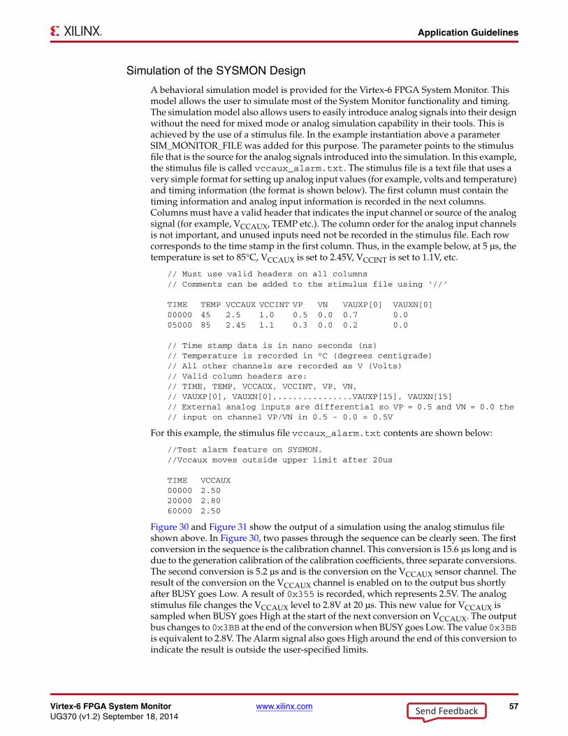
Virtex-6 FPGA System Monitor www.xilinx.com 57UG370 (v1.2) September 18, 2014
Application Guidelines
Simulation of the SYSMON Design
A behavioral simulation model is provided for the Virtex-6 FPGA System Monitor. This model allows the user to simulate most of the System Monitor functionality and timing. The simulation model also allows users to easily introduce analog signals into their design without the need for mixed mode or analog simulation capability in their tools. This is achieved by the use of a stimulus file. In the example instantiation above a parameter SIM_MONITOR_FILE was added for this purpose. The parameter points to the stimulus file that is the source for the analog signals introduced into the simulation. In this example, the stimulus file is called vccaux_alarm.txt. The stimulus file is a text file that uses a very simple format for setting up analog input values (for example, volts and temperature) and timing information (the format is shown below). The first column must contain the timing information and analog input information is recorded in the next columns. Columns must have a valid header that indicates the input channel or source of the analog signal (for example, VCCAUX, TEMP etc.). The column order for the analog input channels is not important, and unused inputs need not be recorded in the stimulus file. Each row corresponds to the time stamp in the first column. Thus, in the example below, at 5 µs, the temperature is set to 85°C, VCCAUX is set to 2.45V, VCCINT is set to 1.1V, etc.
// Must use valid headers on all columns// Comments can be added to the stimulus file using ‘//’
TIME TEMP VCCAUX VCCINT VP VN VAUXP[0] VAUXN[0]00000 45 2.5 1.0 0.5 0.0 0.7 0.005000 85 2.45 1.1 0.3 0.0 0.2 0.0
// Time stamp data is in nano seconds (ns)// Temperature is recorded in °C (degrees centigrade)// All other channels are recorded as V (Volts)// Valid column headers are:// TIME, TEMP, VCCAUX, VCCINT, VP, VN, // VAUXP[0], VAUXN[0],...............VAUXP[15], VAUXN[15]// External analog inputs are differential so VP = 0.5 and VN = 0.0 the // input on channel VP/VN in 0.5 - 0.0 = 0.5V
For this example, the stimulus file vccaux_alarm.txt contents are shown below:
//Test alarm feature on SYSMON.//Vccaux moves outside upper limit after 20us
TIME VCCAUX00000 2.5020000 2.8060000 2.50
Figure 30 and Figure 31 show the output of a simulation using the analog stimulus file shown above. In Figure 30, two passes through the sequence can be clearly seen. The first conversion in the sequence is the calibration channel. This conversion is 15.6 µs long and is due to the generation calibration of the calibration coefficients, three separate conversions. The second conversion is 5.2 µs and is the conversion on the VCCAUX sensor channel. The result of the conversion on the VCCAUX channel is enabled on to the output bus shortly after BUSY goes Low. A result of 0x355 is recorded, which represents 2.5V. The analog stimulus file changes the VCCAUX level to 2.8V at 20 µs. This new value for VCCAUX is sampled when BUSY goes High at the start of the next conversion on VCCAUX. The output bus changes to 0x3BB at the end of the conversion when BUSY goes Low. The value 0x3BB is equivalent to 2.8V. The Alarm signal also goes High around the end of this conversion to indicate the result is outside the user-specified limits.
Send Feedback
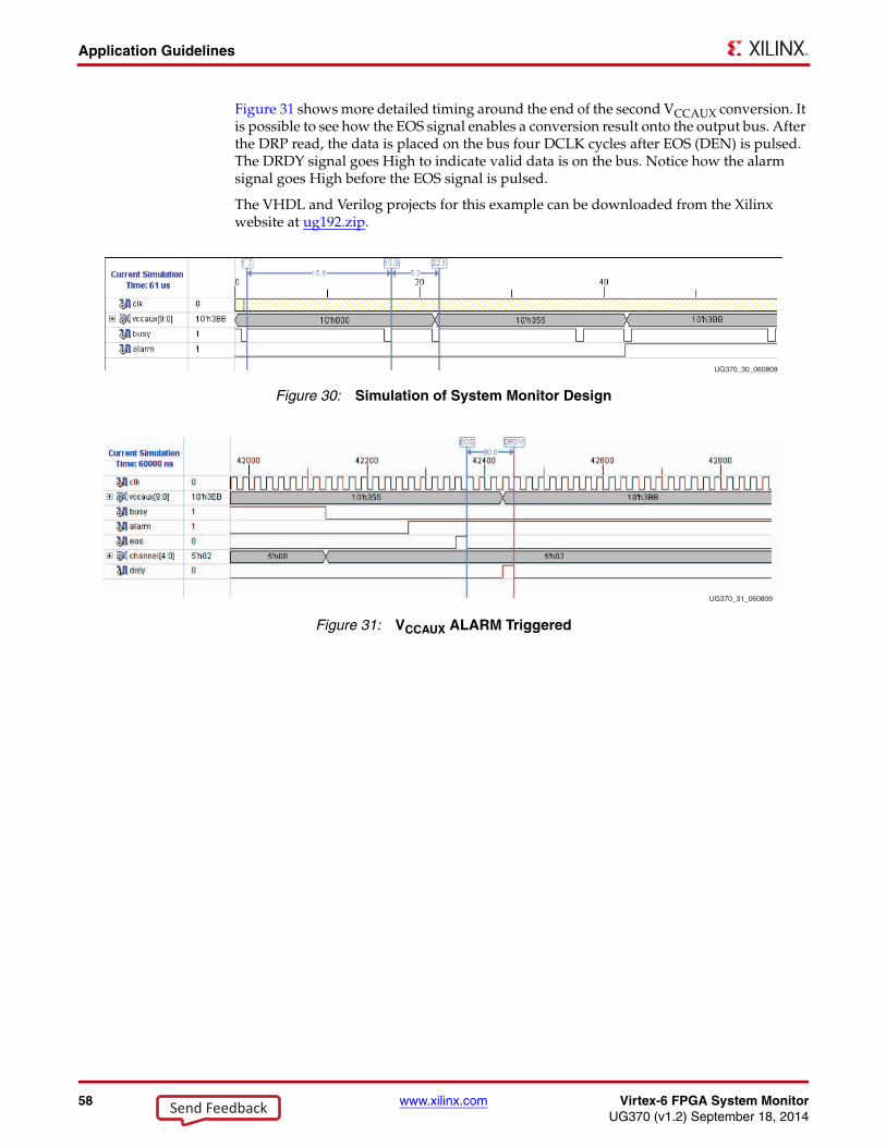
58 www.xilinx.com Virtex-6 FPGA System MonitorUG370 (v1.2) September 18, 2014
Application Guidelines
Figure 31 shows more detailed timing around the end of the second VCCAUX conversion. It is possible to see how the EOS signal enables a conversion result onto the output bus. After the DRP read, the data is placed on the bus four DCLK cycles after EOS (DEN) is pulsed. The DRDY signal goes High to indicate valid data is on the bus. Notice how the alarm signal goes High before the EOS signal is pulsed.
The VHDL and Verilog projects for this example can be downloaded from the Xilinx website at ug192.zip.
X-Ref Target - Figure 30
Figure 30: Simulation of System Monitor Design
UG370_30_060809
X-Ref Target - Figure 31
Figure 31: VCCAUX ALARM Triggered
UG370_31_060809
Send Feedback
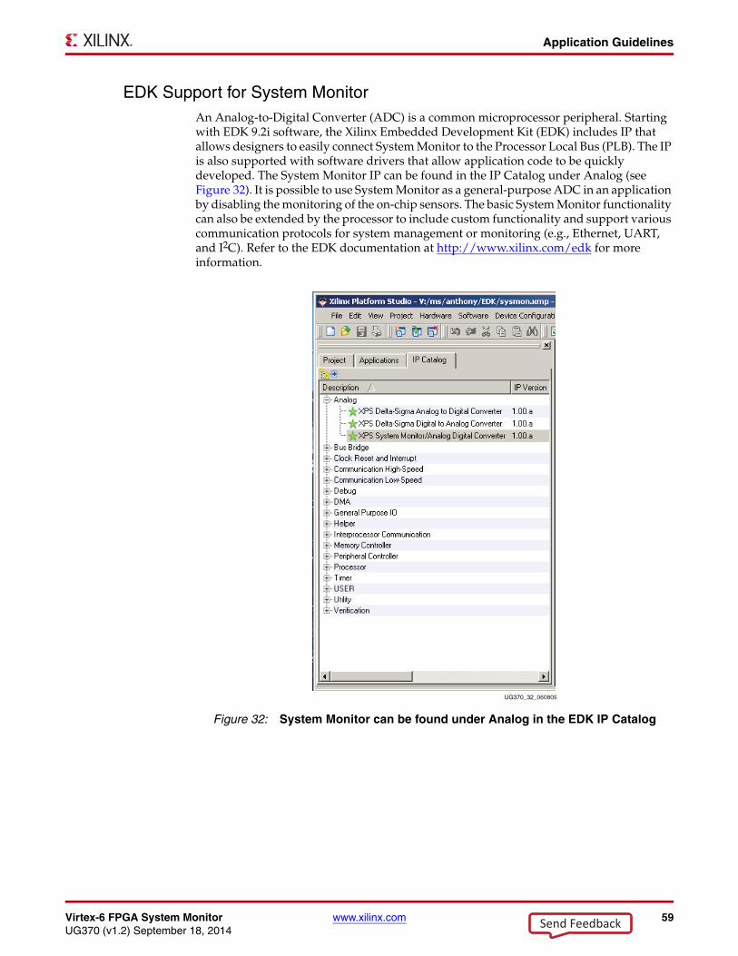
Virtex-6 FPGA System Monitor www.xilinx.com 59UG370 (v1.2) September 18, 2014
Application Guidelines
EDK Support for System MonitorAn Analog-to-Digital Converter (ADC) is a common microprocessor peripheral. Starting with EDK 9.2i software, the Xilinx Embedded Development Kit (EDK) includes IP that allows designers to easily connect System Monitor to the Processor Local Bus (PLB). The IP is also supported with software drivers that allow application code to be quickly developed. The System Monitor IP can be found in the IP Catalog under Analog (see Figure 32). It is possible to use System Monitor as a general-purpose ADC in an application by disabling the monitoring of the on-chip sensors. The basic System Monitor functionality can also be extended by the processor to include custom functionality and support various communication protocols for system management or monitoring (e.g., Ethernet, UART, and I2C). Refer to the EDK documentation at http://www.xilinx.com/edk for more information.X-Ref Target - Figure 32
Figure 32: System Monitor can be found under Analog in the EDK IP Catalog
UG370_32_060809
Send Feedback
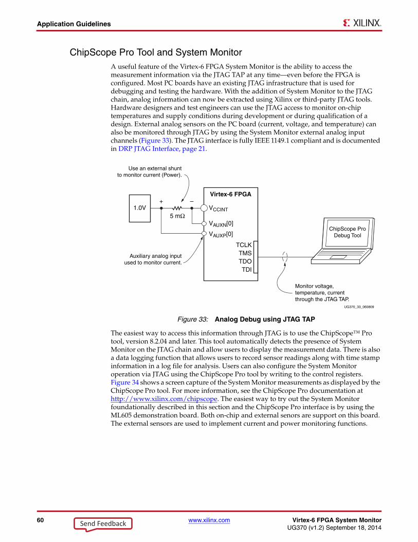
60 www.xilinx.com Virtex-6 FPGA System MonitorUG370 (v1.2) September 18, 2014
Application Guidelines
ChipScope Pro Tool and System MonitorA useful feature of the Virtex-6 FPGA System Monitor is the ability to access the measurement information via the JTAG TAP at any time—even before the FPGA is configured. Most PC boards have an existing JTAG infrastructure that is used for debugging and testing the hardware. With the addition of System Monitor to the JTAG chain, analog information can now be extracted using Xilinx or third-party JTAG tools. Hardware designers and test engineers can use the JTAG access to monitor on-chip temperatures and supply conditions during development or during qualification of a design. External analog sensors on the PC board (current, voltage, and temperature) can also be monitored through JTAG by using the System Monitor external analog input channels (Figure 33). The JTAG interface is fully IEEE 1149.1 compliant and is documented in DRP JTAG Interface, page 21.
The easiest way to access this information through JTAG is to use the ChipScope™ Pro tool, version 8.2.04 and later. This tool automatically detects the presence of System Monitor on the JTAG chain and allow users to display the measurement data. There is also a data logging function that allows users to record sensor readings along with time stamp information in a log file for analysis. Users can also configure the System Monitor operation via JTAG using the ChipScope Pro tool by writing to the control registers. Figure 34 shows a screen capture of the System Monitor measurements as displayed by the ChipScope Pro tool. For more information, see the ChipScope Pro documentation at http://www.xilinx.com/chipscope. The easiest way to try out the System Monitor foundationally described in this section and the ChipScope Pro interface is by using the ML605 demonstration board. Both on-chip and external senors are support on this board. The external sensors are used to implement current and power monitoring functions.
X-Ref Target - Figure 33
Figure 33: Analog Debug using JTAG TAP
Virtex-6 FPGA
VCCINT1.0V5 mΩ
+ –
VAUXN[0]
TCLKTMSTDOTDI
VAUXP[0]ChipScope Pro
Debug Tool
Monitor voltage,temperature, currentthrough the JTAG TAP.
UG370_33_060809
Use an external shuntto monitor current (Power).
Auxiliary analog inputused to monitor current.
Send Feedback
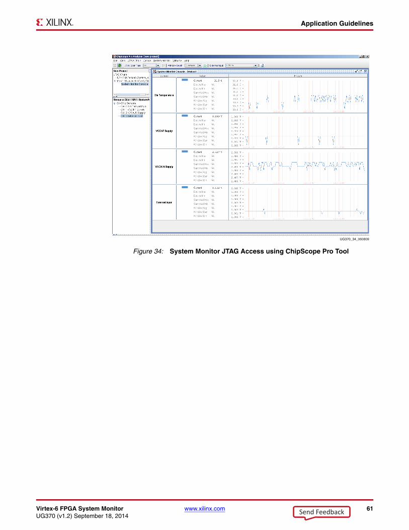
Virtex-6 FPGA System Monitor www.xilinx.com 61UG370 (v1.2) September 18, 2014
Application Guidelines
X-Ref Target - Figure 34
Figure 34: System Monitor JTAG Access using ChipScope Pro Tool
UG370_34_060809
Send Feedback
62 www.xilinx.com Virtex-6 FPGA System MonitorUG370 (v1.2) September 18, 2014
Application Guidelines
Send Feedback