valley polarization in mos 2 monolayers by optical pumpingli.mit.edu/s/2d/paper/zeng12dai.pdf ·...
TRANSCRIPT

Valley polarization in MoS2 monolayers byoptical pumpingHualing Zeng1†, Junfeng Dai2,1†, Wang Yao1,3, Di Xiao4 and Xiaodong Cui1*
Most electronic devices exploit the electric charge of electrons,but it is also possible to build devices that rely on other prop-erties of electrons. Spintronic devices, for example, make useof the spin of electrons1,2. Valleytronics is a more recent devel-opment that relies on the fact that the conduction bands ofsome materials have two or more minima at equal energiesbut at different positions in momentum space3–5. To make avalleytronic device it is necessary to control the number ofelectrons in these valleys, thereby producing a valley polariz-ation6–11. Single-layer MoS2 is a promising material for valley-tronics because both the conduction and valence band edgeshave two energy-degenerate valleys at the corners of the firstBrillouin zone12. Here, we demonstrate that optical pumpingwith circularly polarized light can achieve a valley polarizationof 30% in pristine monolayer MoS2. Our results, and similarresults by Mak et al.13, demonstrate the viability of opticalvalley control and valley-based electronic and optoelectronicapplications in MoS2 monolayers.
In many crystalline materials, it often happens that the conduc-tion-band minima and valence-band maxima are located at degener-ate and inequivalent valleys in momentum space. The valley indexcan be regarded as a discrete degree of freedom for low-energycarriers, which is robust against smooth deformation and low-energy phonons because of the large valley separation in momentumspace. To make use of the valley index as an information carrier, thecrucial step is to identify a process in which the valley carriersrespond differently to external stimuli. Recently, a simple schemebased on inversion symmetry breaking has been proposed torealize the manipulation of the valley index through electric, mag-netic and optical means5,11. In particular, it was shown that inversionsymmetry breaking can lead to contrasting circular dichroism indifferent k-space regions, which takes the extreme form of contrast-ing optical selection rules at the high symmetry points of theBrillouin zone11. This enables a valley-dependent interplay ofelectrons with light of different circular polarizations, in analogyto the spin-dependent optical activities in semiconductors suchas GaAs.
Here, we report our observation of selective photoexcitation ofthe degenerate valleys by circularly polarized optical pumping inMoS2 monolayers, an emerging multi-valley two-dimensional semi-conductor with remarkable optical and transport properties14,15.Bulk MoS2 has a hexagonal-crystal layered structure with a covalentlybonded S–Mo–S hexagonal quasi-two-dimensional network packedby weak van der Waals forces. Previous studies have shown that, witha decrease in thickness, MoS2 crosses over from being an indirect-bandgap semiconductor (with multiple layers) to a direct-bandgapsemiconductor (as a monolayer)15,16. The direct bandgap is in thevisible frequency range (�1.9 eV) and is therefore ideal for optical
applications, with both conduction and valence band edges locatedat the K (K′) points of the two-dimensional hexagonal Brillouinzone. In addition to the changes to its electronic structure, MoS2thin film also undergoes a structural change, as outlined in Fig. 1a.The inversion symmetry present in bulk and in thin films with aneven number of layers is explicitly broken in thin films with an oddnumber of layers, giving rise to a valley-contrasting optical selectionrule11,12,17, where the inter-band transitions in the vicinity of theK (K′) point couple exclusively to right (left)-handed circularlypolarized light sþ (s–) (Fig. 1). The direct-bandgap transition atthe two degenerate valleys, together with this valley-contrastingselection rule, suggest that one can optically generate and detectvalley polarizations in a MoS2 monolayer.
Our main result is summarized in the following. We find that inMoS2 monolayers, the photoluminescence has the same helicity inits circularly polarized component as the excitation laser, a signatureof optically pumped valley polarization. Below 90 K, a highphotoluminescence circular polarization is observed, which decayswith temperature. The photoluminescence polarization shows nodependence on the in-plane magnetic field. The absence of theHanle effect is a strong indicator that the polarized photolumines-cence arises from the polarization of the valley rather than spin,as the former cannot be rotated by the magnetic field. Moreover,in MoS2 bilayers, we find that photoluminescence from MoS2bilayers is unpolarized under the same excitation conditions,consistent with the presence of inversion symmetry.
MoS2 flakes, shown representatively in Fig. 2a, were mechanicallyexfoliated from SiO2/silicon substrates using sticky tape in amanner similar to the technique used to produce graphene sheets.The monolayer, bilayer and multilayer flakes could be identified bytwo characteristic Raman modes: the in-plane vibrational E2g
1 modeand the out-of-plane vibrational A1g mode around 400 cm21
(ref. 14). Following ref. 14, we labelled the sample thickness accordingto the frequency difference between the E2g
1 and A1g modes:Dv¼ 19 cm21 indicating monolayers and Dv¼ 21 cm21
bilayers (Fig. 2b). The layer assignment was confirmed by atomicforce microscopy (AFM). Photoluminescence spectra around1.9 eV, corresponding to excitons from the direct inter-bandtransition18, were also used as a monolayer and bilayer indicatorfrom the transition from indirect- to direct-gapped semiconductor,as illustrated in refs 15,16.
The polarization-sensitive photoluminescence measurement wascarried out using a confocal-like microscopic set-up. The collimatedbackscattering light was passed through a broadband 1/4l waveplate, a beam-displacing prism to separate the light beam into twoorthogonally polarized beams and a depolarizer, and was thenfocused to two spots at the entrance slit of the monochromatorequipped with a charge-coupled device (CCD) camera. The
1Physics Department, The University of Hong Kong, Pokfulam road, Hong Kong, China, 2Department of Physics, South University of Science and Technologyof China, Shenzhen 518055, China, 3Center of Theoretical and Computational Physics, The University of Hong Kong, Hong Kong, China, 4Materials Scienceand Technology Division, Oak Ridge National Laboratory, Oak Ridge, Tennessee 37831, USA, †These authors contributed equally to this work.
*e-mail: [email protected]
LETTERSPUBLISHED ONLINE: 17 JUNE 2012 | DOI: 10.1038/NNANO.2012.95
NATURE NANOTECHNOLOGY | VOL 7 | AUGUST 2012 | www.nature.com/naturenanotechnology490
© 2012 Macmillan Publishers Limited. All rights reserved.

polarization resolved spectrum could then be obtained by analysingthe two branches of dispersion on the CCD. (For details regardingthe set-up, see Supplementary Information.)
Figure 2c presents the circularly polarized luminescence spectraof a pristine MoS2 monolayer, which peak around 1.9 eV with right-and left-handed circularly polarized excitation (HeNe laser,1.96 eV) at a near-resonant condition at T¼ 10 K. The lumines-cence corresponds to a direct inter-band transition at the K (K′)valley. The helicity of the luminescence exactly follows that of theexcitation light. In other words, the right-handed circularlypolarized excitation generates right-handed luminescence, and theleft-handed circularly polarized excitation generates left-handedluminescence. To characterize the circular component in the lumi-nescence spectra, we define the degree of circular polarization
P = I(s+) − I(s−)I(s+) + I(s−)
where I(s+) is the intensity of the left (right)-handed circularcomponent. For perfectly circularly polarized light, P¼ 1 (sþ) or–1 (s2) (for details see Supplementary Information). The lumines-cence spectra demonstrate a symmetric polarization for excitationwith opposite helicities: P¼ 0.32 under sþ excitation andP¼20.32 under s2 excitation for the most representative MoS2monolayer out of four samples that gave values of P¼+0.23,+0.25, +0.28 and +0.32 under s+ excitation, respectively, at10 K. This behaviour is fully expected under the mechanism ofthe valley-dependent optical selection rule. As well as the unpolar-ized background, there is also a linearly polarized component, andthe linear polarization shifts by �258 between sþ and s2 exci-tation. If one switches the excitation light to a higher energy at2.33 eV, no polarization can be observed in the luminescencespectra. We note that the valley selection rule is valid in the vicinityof the K (K′) point11,12, whereas the optical transition with 2.33 eVoccurs far away from the K points in band dispersion.
MonolayerBulk
10 μmBilayer
a
b
c
350 400 450 500
Monolayer
Si
A1gE 12g
BilayerBulk
550 1.80
−500
−250
0
Circ
ular
lum
ines
cenc
e (a
.u.)
250
500
750
1.82 1.84 1.86 1.88 1.90Photon energy (eV)
Pσ− = −32 ± 2%
Pσ+ = 32 ± 2%
Left-handed circular excitation
Right-handed circular excitation
Raman shift (cm−1)
Inte
nsity
(a.u
.)
Figure 2 | Polarization-sensitive photoluminescence spectra from MoS2 monolayers. a, Representative optical image of MoS2 monolayer, bilayer and thin-
film flakes. b, Characteristic Raman spectra from different MoS2 flakes (monolayer, bilayer and thin film), showing an in-plane vibrational E2g1 mode and an
out-of-plane vibrational A1g mode around 400 cm21. c, Polarization resolved luminescence spectra under circularly polarized excitation from a HeNe laser at
1.96 eV and 10 K. Circular polarizations of P¼ 32+2% and 232+2% are observed along the out-of-plane direction with right- and left-handed circular
excitation, respectively.
S
Mo
K
K’
K K’
K
K’
a b
K K’
σ− σ+
Figure 1 | Schematic of MoS2 monolayer and optical selection rules at K(K’) point. a, Schematic of MoS2 monolayer structure (left) and bulk unit cell
(right), clearly showing the spatial inversion symmetry breaking in monolayers. b, Schematic of proposed valley-dependent selection rules at K and K′ points
in crystal momentum space: left (right)-handed circularly polarized light sþ (s2) only couples to the band-edge transition at K (K′) points for the sake of
angular moment conservation and time reversal symmetry.
NATURE NANOTECHNOLOGY DOI: 10.1038/NNANO.2012.95 LETTERS
NATURE NANOTECHNOLOGY | VOL 7 | AUGUST 2012 | www.nature.com/naturenanotechnology 491
© 2012 Macmillan Publishers Limited. All rights reserved.

In many semiconductor systems such as GaAs bulk and hetero-structures, the circular polarization of luminescence from circularlypolarized excitation originates from electron (hole) spin polariz-ation as a result of the spin-dependent optical selection rule19,20.This mechanism can be excluded here by examining the changein the photoluminescence spectra in an in-plane magnetic field(Fig. 3a). With a non-zero in-plane g-factor, spin polarizationwill precess about the in-plane magnetic field, and the time averageof the spin projected along the z-axis will be foundat Sz =
�t0 SZ0 exp(−t/tS) cos(gmBBt/h− )dt, where SZ0 is the initial
spin along the z-axis, tS is the spin relaxation time, mB is the Bohrmagneton and t is the lifetime of the photoexcited carriers.Consequently, the polarization of the luminescence under continu-ous-wave excitation should follow
P(B) ≈ P(B = 0)1 + (gmBBtS/h− )2
where P(B ¼ 0) is the polarization of the luminescence without themagnetic field. This is the well-known Hanle effect. If we assumethat the spin relaxation time tS is of approximately the same orderas the photocarrier lifetime t≈ 10 ps (ref. 21), then the polarizationP(B¼ 0.65T) will drop to a few per cent of P(B¼ 0). As shown inFig. 3a, however, there is no visible difference between the photolu-minescence polarization at zero field and in an in-plane field ofB¼ 0.65T. Therefore, spin polarization cannot explain the polarizedphotoluminescence observed here. Instead, this magnetic-field-inde-pendent photoluminescence polarization is a fully expected conse-quence of valley polarization through the valley-dependentselection rule; because the in-plane magnetic field does not coupleto the valley index, the valley polarization cannot be rotated by themagnetic field, so no Hanle effect can be observed.
Further evidence for attributing the polarized photolumines-cence in monolayers to the valley-dependent optical selection rulecan be found from a comparison with photoluminescence spectrafrom MoS2 bilayers (Fig. 3b). The intensity of the luminescence inbilayers is relatively weaker than that of monolayers, with the strik-ing difference being that the circular polarization of luminescencefrom bilayers is negligible under the same conditions. This differ-ence can be easily understood: the polarized photoluminescence isa consequence of the valley-dependent optical selection rulearising from inversion symmetry breaking in MoS2 monolayerswith D3h
1 symmetry12. In contrast, MoS2 bilayers are composed oftwo structurally identical monolayers stacking with hexagonalsymmetry (the sulphur atoms in one layer sit directly upon/belowthe molybdenum atoms in the other) and have D6h
4 symmetry.Inversion symmetry is preserved in the bilayer unit cell, so thevalley-dependent selection rule is not allowed in bilayers11. If theexcitation power is increased above 1 × 10⁵ W cm22, circularlypolarized photoluminescence is observed in bilayers, suggestingthat the heating effects could induce structural anisotropy andconsequently break the inversion symmetry in the bilayer.
Figure 4 displays the typical temperature dependence of thecircular polarization of luminescence from monolayers undercircularly polarized excitation. The circular polarization has a flatplateau at�31% below 90 K, then dramatically drops with increasingtemperature. The small temperature dependence of the polarizationat low temperatures implies that the inter-valley scattering (K ↔ K′)results mainly from scattering at grain boundaries and atomicallysharp deformations. Because the sample is a natural miningproduct, abundant impurities and vacancies presumably provideinter-valley scattering centres and populate conduction electrons atthe energetically degenerate K and K′ valleys. The linearly polarizedcomponent of luminescence also suggests possible coherent mixingof the two valleys.
HeNe laser
Monolayer MoS2
Monolayer
Circ
ular
lum
ines
cenc
e (a
.u.)
Circ
ular
lum
ines
cenc
e (a
.u.)
Monolayer
Phot
olum
ines
cenc
e (a
.u.)
Bilayer
Bilayer
1.75
800
600
400
200
0
S
Mo
6.5 Å
2.00
SiO2/Si substrate
B = 0T
B = 0.65T
1.80 1.85
0
200
400
600
800a
1.90 1.80 1.85 1.90Photon energy (eV) Photon energy (eV)
B
Photoluminescence
b
Figure 3 | Photoluminescence under an in-plane magnetic field and from bilayers. a, Circularly polarized components of luminescence spectra at zero
magnetic field (black) and under an in-plane magnetic field of 0.65T (red). The two curves overlap within the resolution of the apparatus. b, Upper left inset:
schematic of a MoS2 bilayer unit cell. Upper right inset: photoluminescence spectra of monolayer (blue) and bilayer (green) MoS2 under the same conditions
(base temperature, 10 K; 0.2 mW linearly polarized excitation at 1.96 eV). The intensity of the bilayer luminescence is slightly weaker than that of the
monolayer. Main panel: circularly polarized components of luminescence spectra from MoS2 bilayers (green) and monolayers (blue) under circular excitation
at 1.96 eV and 10 K. Negligible circular polarization is observed for the MoS2 bilayers.
LETTERS NATURE NANOTECHNOLOGY DOI: 10.1038/NNANO.2012.95
NATURE NANOTECHNOLOGY | VOL 7 | AUGUST 2012 | www.nature.com/naturenanotechnology492
© 2012 Macmillan Publishers Limited. All rights reserved.
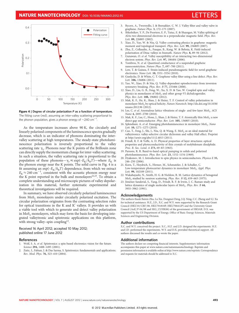
As the temperature increases above 90 K, the circularly andlinearly polarized components of the luminescence spectra graduallydecrease, which is an indicator of phonons dominating the inter-valley scattering at high temperatures. The steady-state photolumi-nescence polarization is inversely proportional to the valleyscattering rate gn. Phonons near the K points of the Brillouin zonecan directly supply the momentum change for inter-valley scattering.In such a situation, the valley scattering rate is proportional to thepopulation of these phonons—gn/ exp(–EK/kBT)—where EK isthe phonon energy near the K points. The solid curve in Fig. 4 is afit assuming an exp(–EK/kBT) dependence, from which we extractEK ≈ 240 cm21, consistent with the acoustic phonon energy nearthe K point reported in the bulk and monolayers22,23. To obtain acomplete understanding and microscopic pictures of valley depolar-ization in this material, further systematic experimental andtheoretical investigations will be required.
In summary, we have observed circularly polarized luminescencefrom MoS2 monolayers under circularly polarized excitation. Thecircular polarization originates from the contrasting selection rulesfor optical transitions in the K and K′ valleys. It provides us witha viable tool with which to generate and detect valley polarizationin MoS2 monolayers, which may form the basis for developing inte-grated valleytronic and spintronic applications on this platform,with strong valley–spin coupling12.
Received 16 April 2012; accepted 10 May 2012;published online 17 June 2012
References1. Wolf, S. A. et al. Spintronics: a spin-based electronics vision for the future.
Science 294, 1488–1495 (2001).2. Zutic, I., Fabian, J. & Das Sarma, S. Spintronics: fundamentals and applications.
Rev. Mod. Phys. 76, 323–410 (2004).
3. Rycerz, A., Tworzydlo, J. & Beenakker, C. W. J. Valley filter and valley valve ingraphene. Nature Phys. 3, 172–175 (2007).
4. Shkolnikov, Y. P., De Poortere, E. P., Tutuc, E. & Shayegan, M. Valley splitting ofAlAs two-dimensional electrons in a perpendicular magnetic field. Phys. Rev.Lett. 89, 226805 (2002).
5. Xiao, D., Yao, W. & Niu, Q. Valley-contrasting physics in graphene: magneticmoment and topological transport. Phys. Rev. Lett. 99, 236809 (2007).
6. Zhu, Z., Collaudin, A., Fauque, B., Kang, W. & Behnia, K. Field-inducedpolarization of Dirac valleys in bismuth. Nature Phys. 8, 89–94 (2012).
7. Gunawan, O. et al. Valley susceptibility of an interacting two-dimensionalelectron system. Phys. Rev. Lett. 97, 186404 (2006).
8. Tombros, N. et al. Quantized conductance of a suspended graphenenanoconstriction. Nature Phys. 7, 697–700 (2011).
9. Low, T. & Guinea, F. Strain-induced pseudomagnetic field for novel grapheneelectronics. Nano Lett. 10, 3551–3554 (2010).
10. Gunlycke, D. & White, C. T. Graphene valley filter using a line defect. Phys. Rev.Lett. 106, 136806 (2011).
11. Yao, W., Xiao, D. & Niu, Q. Valley-dependent optoelectronics from inversionsymmetry breaking. Phys. Rev. B 77, 235406 (2008).
12. Xiao, D., Liu, G. B., Feng, W., Xu, X. D. & Yao, W. Coupled spin and valleyphysics in monolayers of MoS2 and other group-VI dichalcogenides.Phys. Rev. Lett. 108, 196802 (2012).
13. Mak, K. F., He, K., Shan, J. & Heinz, T. F. Control of valley polarization inmonolayer MoS2 by optical helicity. Nature Nanotech. http://dx.doi.org/10.1038/nnano.2012.96 (2012).
14. Lee, C. et al. Anomalous lattice vibrations of single- and few-layer MoS2. ACSNano 4, 2695–2700 (2010).
15. Mak, K. F., Lee, C., Hone, J., Shan, J. & Heinz, T. F. Atomically thin MoS2: a newdirect-gap semiconductor. Phys. Rev. Lett. 105, 136805 (2010).
16. Splendiani, A. et al. Emerging photoluminescence in monolayer MoS2. NanoLett. 10, 1271–1275 (2010).
17. Cao, T., Feng, J., Shi, J., Niu, Q. & Wang, E. MoS2 as an ideal material forvalleytronics: valley-selective circular dichroism and valley Hall effect. Preprintat http://arxiv.org/abs/1112.4013 (2011).
18. Frindt, R. F. & Yoffe, A. D. Physical properties of layer structures: opticalproperties and photoconductivity of thin crystals of molybdenum disulphide.Proc. R. Soc. Lond. A 273, 69–83 (1963).
19. Parsons, R. R. Band-to-band optical pumping in solids and polarizedphotoluminescence. Phys. Rev. Lett. 23, 1152–1154 (1969).
20. Dyakonov, M. I. Introduction to spin physics in semiconductors. Physica E 35,246–250 (2006).
21. Korn, T., Heydrich, S., Hirmer, M., Schmutzler, J. & Schuller, C.Low-temperature photocarrier dynamics in monolayer MoS2. Appl. Phys.Lett. 99, 102109 (2011).
22. Wakabayashi, N., Smith, H. G. & Nicklow, R. M. Lattice dynamics of hexagonalMoS2 studied by neutron scattering. Phys. Rev. B 12, 659–663 (1975).
23. Jimenez Sandoval, S., Yang, D., Frindt, R. F. & Irwin, J. C. Raman study andlattice dynamics of single molecular layers of MoS2. Phys. Rev. B 44,3955–3962 (1991).
AcknowledgementsThe authors thank Bairen Zhu, Lu Xie, Dongmei Deng, J.Q. Ning, C.C. Zheng and S.J. Xufor technical assistance. H.Z., J.D., X.C. and W.Y. were supported by the Research GrantCouncil (HKU10/CRF/08, HKU701810P, HKU706412P) and the University GrantCouncil (AoE/P-04/08 and SEG_CUHK06) of the government of HKSAR. D.X. wassupported by the US Department of Energy, Office of Basic Energy Sciences, MaterialsSciences and Engineering Division.
Author contributionsX.C. and W.Y. conceived the project. X.C., H.Z. and J.D. designed the experiments. H.Z.and J.D. performed the experiments. W.Y. and D.X. provided theoretical support. Allauthors discussed the results and co-wrote the paper.
Additional informationThe authors declare no competing financial interests. Supplementary informationaccompanies this paper at www.nature.com/naturenanotechnology. Reprints andpermission information is available online at http://www.nature.com/reprints. Correspondenceand requests for materials should be addressed to X.C.
0.4
0.3
0.2
0.1
0.0
0 50 100 150 200 250 300Temperature (K)
Pola
rizat
ion
Polarization
Fitting curve
Figure 4 | Degree of circular polarization P as a function of temperature.
The fitting curve (red), assuming an inter-valley scattering proportional to
the phonon population, gives a phonon energy of �240 cm21.
NATURE NANOTECHNOLOGY DOI: 10.1038/NNANO.2012.95 LETTERS
NATURE NANOTECHNOLOGY | VOL 7 | AUGUST 2012 | www.nature.com/naturenanotechnology 493
© 2012 Macmillan Publishers Limited. All rights reserved.