universal charger for car battery design modifications...
TRANSCRIPT
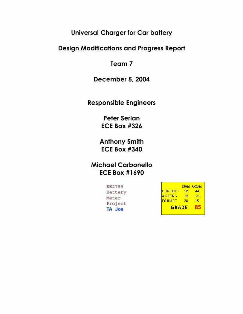
Universal Charger for Car battery
Design Modifications and Progress Report
Team 7
December 5, 2004
Responsible Engineers
Peter Serian ECE Box #326
Anthony Smith ECE Box #340
Michael Carbonello
ECE Box #1690

i
TABLE OF CONTENTS
1. Introduction……………………………………………………... …. 1 2. Design Modifications………………………………………………. 2 3. Overview of Revised Design………………………………………. 5 3.1. AC/DC Conversion Circuit…………………………….. 7
3.2. Charging Circuit and Cooling………………………….. 9 3.3. Overcharge Protection Circuit………………………….. 11 3.4. Casing…………………………………………………... 13 3.5. Display………………………………………………….. 15
4. Revised Project Schedule…………………………………………... 17 5. Conclusion…………………………………………………………. 19 6. References………………………………………………………….. 20
ii
TABLE OF FIGURES Figure 1: System Block Diagram for the Universal Car Battery Charger 6 Figure 2: Original AC/DC Conversion Circuit 7 Figure 3: Revised AC/DC Conversion Circuit 8 Figure 4: Revised Regulation Circuitry 9 Figure 5: The Overcharge Protection Circuit 11 Figure 6: A Visually Impressive Case 14 Figure 7: Our Case 14 Figure 8: Our updated Gantt Chart 17

1
1. Introduction
This report explains to the reader all of the design modifications and progressions that
have taken place since the last progress report was submitted on November 24, 2003. As
part of the design process, some elements of the universal battery charger have changed.
Other elements, which we did not have time to consider before that date, have now been
added to the design. After reading this report, the reader should have a good
understanding of all of the revisions to our project, including the overall design and our
project schedule.
The original design for the battery charger consisted of three main modules: the
AC/DC conversion circuit, the charging circuit, and the overcharge protection circuit,
which were to be supported by other important modules such as the cooling system and
casing. This remains our overall design approach. However, extensive revisions have
been made to each of the three main modules based on new information about the
components we have selected and the inputs we will be receiving. In addition, the cooling
system and casing designs, which were considered secondary to the charging circuitry a
couple of weeks ago, have now materialized. All in all, the design changes made do not
reflect a departure from our original design, but rather a fluid progression toward
implementing it.

2
2. Design Modifications
Several small changes were made to each of the three main circuits. The AC/DC
conversion circuit remains essentially the same. After discussing the circuit together, we
found that the possibility of voltage spikes had not been addressed by our design. Thus,
the only real change made to this circuit was the inclusion of a voltage suppressing
device to handle power surges.
The corrections of the errors in the regulation circuit were essential to ensure
appropriate functionality of the circuit. First, we realized that the input current and
voltage going into the regulator being reduced to the output current and voltage was
going to dissipate substantial power, and we needed to compensate for excessive heat
production. We chose to implement a heat sink on the surface of the voltage regulation
IC. Fortunately, the package of the regulator, TO-220, is very common and gave us some
flexibility in choosing the most suitable heat sink. Furthermore, the voltage regulator
was originally configured to output 15 volts, and when the battery drained the maximum
current of 2 A, it would be charging at 14.8 volts because of the voltage drop across the
sensor resistor. However, this was higher than our original intended charging voltage of
14.7 volts, and even worse, when the battery started to draw less and less current, the
voltage applied to it could raise as high as 14.95 volts, or the high charging voltage might
force the battery to draw more current than it should for a longer period of time than it
should. In this situation, by the time the overcharge protection circuit kicked in, it might
be too late. This problem can be fixed by changing the adjustable resistor values.
Another problem we had to overcome was that we used resistor values and a capacitor
value that were not available in the ECE kit or ECE shop. While these will be fine for our
final design, we would like to use more common, available resistors for our prototypes.
The first resistor value that needed modification, a 2.5kΩ resistor, was one that was
activated by the trickle charge relay. The second resistor value that was not available was
the 13.7kΩ, which required equivalent circuitry that was in stock as well. The capacitor
value that needed modification, a 3.3uF capacitor, was the capacitor that was positioned
at the output of the regulator. Section 3.2 of this document describes the operation details
of this circuit and the changes we made.
3
The overcharge protection circuit underwent extensive re-configuration, but the basic
principle behind its operation remained the same. Section 3.3 gives an overview of the
operation of this circuit, and within that section, Figure 5 shows the circuit schematic.
The circuit senses the current going to the battery, and when the current drops below 400
mA, the circuit re-configures the charger by activating a relay. One problem was that
when engineering this circuit, we designed the difference amplifier portion to amplify the
difference by a factor of -10, without realizing that the op-amps used cannot produce a
voltage below that of their negative supply rail, which in this case is ground. Therefore, a
voltage gain of -10 was impossible to achieve, since the op-amps are incapable of
outputting a negative voltage. Simply wiring the circuit to have a gain of positive 10
presented a new problem, since the Schmitt trigger sub-circuit cannot have a low
activation threshold that is higher than the low output saturation voltage of the op-amps
used, which is 0.1 volts (For a precise explanation of how the Schmitt trigger works, refer
to our 4th report, the Overall Design Progress Report, section 3.4.2.). The final problem
we discovered with the circuit as previously designed was that if someone hooked a load
up to the battery while it was charging, it would draw extra current from our charger.
This would trick the overcharge protection circuit into thinking that the battery needs to
be charged more, since the circuit assesses the battery’s charge based on the amount of
current leaving the charger. The charger would then continue to charge the battery at a
high voltage, possibly overcharging and ruining it.
To overcome these problems, we first hooked up the difference amplifier portion of
the circuit the opposite way of how it was hooked up before. This overcame the problem
of producing a negative voltage by simply inverting the “terminals” of the difference
amplifier across the sensor resistor. The problem of the activation threshold of the
Schmitt trigger was solved by re-configuring the difference amplifier to have a gain of
only 2, and re-configuring the Schmitt trigger such that its activation threshold was 80
mV instead of -400 mV. This was done by changing the configuration resistor values for
both sub-circuits. Now, when the current reaches the desired switching value of 400 mA,
it produces a 40-mV voltage drop across the 0.1-ohm sensor resistor, which is amplified
by the difference amplifier to be 80 mV, which activates the Schmitt trigger at its new
threshold. The final problem, which occurs when someone hooks up a device to the

4
battery while it is charging, was solved by adding a user option in the form of a switch.
When the user wishes to connect a device to the battery while it is charging, the switch
must be toggled. It activates the relay which re-configures the charging circuit to charge
at the safe trickle voltage. Essentially, this switch is the manual counterpart to the
automatic overcharge protection circuit.
5
3. Overview of Revised Design
The block diagram in Figure 1 shows that the top-level design of our battery charging
unit has not changed. The signal flow from input to output of the device remains the
same, along with the same basic approach, which utilizes an AC/DC conversion circuit, a
cooled charging circuit, and an overcharge protection circuit to turn the input power into
power that can charge our battery. The environment in which these subsystems operate is
regulated by the cooling system of the charging circuit and the casing.

6
Figure 1: System Block Diagram for the Universal Car Battery Charger
7
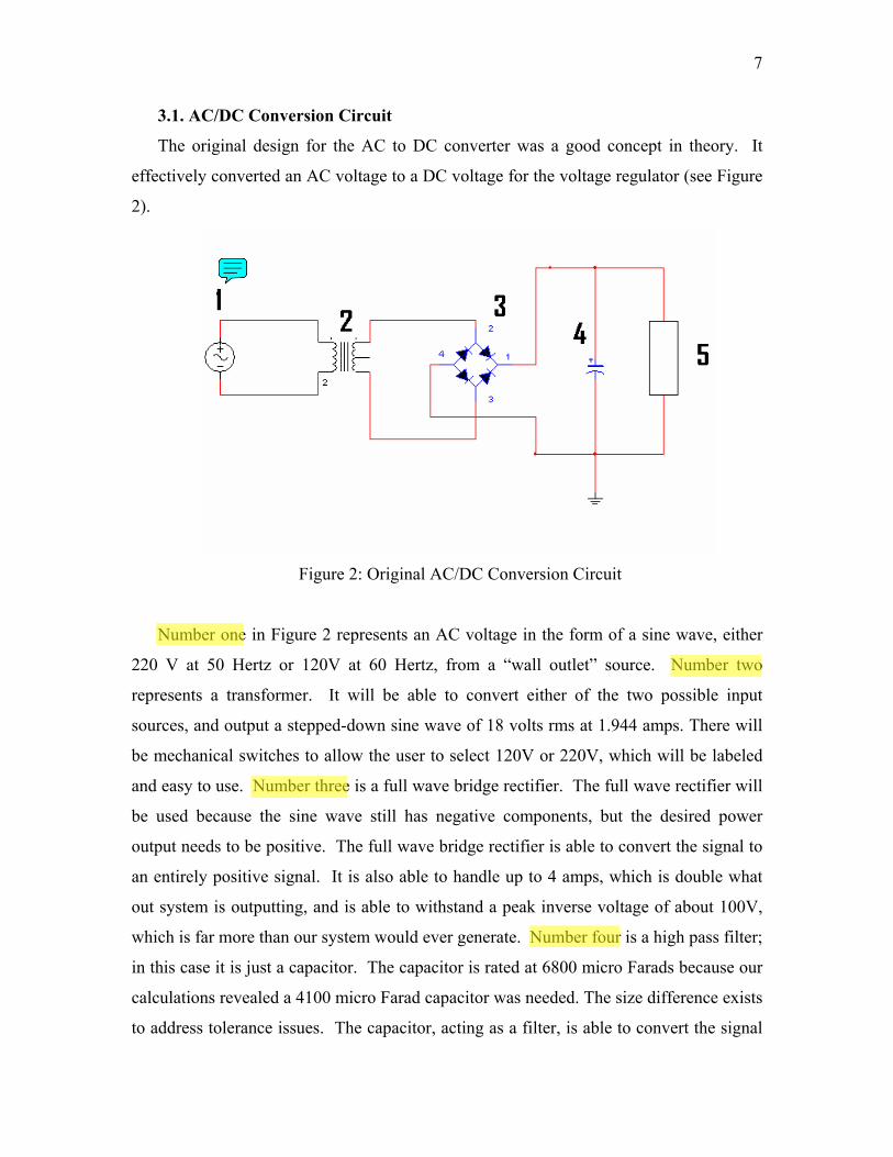
3.1. AC/DC Conversion Circuit
The original design for the AC to DC converter was a good concept in theory. It
effectively converted an AC voltage to a DC voltage for the voltage regulator (see Figure
2).
Figure 2: Original AC/DC Conversion Circuit
Number one in Figure 2 represents an AC voltage in the form of a sine wave, either
220 V at 50 Hertz or 120V at 60 Hertz, from a “wall outlet” source. Number two
represents a transformer. It will be able to convert either of the two possible input
sources, and output a stepped-down sine wave of 18 volts rms at 1.944 amps. There will
be mechanical switches to allow the user to select 120V or 220V, which will be labeled
and easy to use. Number three is a full wave bridge rectifier. The full wave rectifier will
be used because the sine wave still has negative components, but the desired power
output needs to be positive. The full wave bridge rectifier is able to convert the signal to
an entirely positive signal. It is also able to handle up to 4 amps, which is double what
out system is outputting, and is able to withstand a peak inverse voltage of about 100V,
which is far more than our system would ever generate. Number four is a high pass filter;
in this case it is just a capacitor. The capacitor is rated at 6800 micro Farads because our
calculations revealed a 4100 micro Farad capacitor was needed. The size difference exists
to address tolerance issues. The capacitor, acting as a filter, is able to convert the signal

8
from the rectifier to a saw tooth output that is almost a constant voltage. The minor
ripples will then be converted in the next portion of circuit. Number five represents the
next sub-system.
There is one major design omission that cannot be accounted for in most
simulations or calculations, and that is voltage suppression. The voltage and current of a
simulation can account for maximums and minimums as well as tolerances, but it does
not generate spikes, severe drops, or blackout conditions that are common to the power
grid in which our device will be used. A voltage suppressor, number two in Figure 3,
will suppress large spikes that may come from “wall outlets” and protect the rest of the
circuit. The suppressor will be rated to suppress any voltage above 315 V. This is
because the peak voltage from a 220V AC source is about 310 V.
Figure 3: Revised AC/DC Conversion Circuit
Even though the transformer would probably be able to handle some voltage spikes, it
is superior design to include a suppressor. This will make the signal going to the
transformer cleaner and easier for the transformer to handle. If there was a spike large
enough and the suppressor was to be destroyed it would be beneficial to destroy the
suppressor, not the transformer. The suppressor is less than a dollar in cost, and it would
be very easy to replace. The transformer, however, has numerous wires and two

9
switches, which would be much harder to repair or replace, and would cost over fifteen
dollars.
3.2. Charging Circuit and Cooling
Figure 4: Revised Regulation Circuitry
The revised charging circuit is shown in Figure 4. The first set of changes made was
on the external circuitry of the voltage regulator. First, the issue of lowering the output
voltage of the regulator so the overcharge circuitry can be activated was solved by
reverting back to a previous design where we chose resistor values to output 14.8 volts
instead of 15 volts. This way, the lowest charge voltage applied across the battery would
be 14.6, and the highest would be 14.75, values which are much closer to the charging
voltage recommended by manufacturers (www.panasonic.com). The adjustable
resistances were changed to 1k Ω and 2.5kΩ to produce the desired output. The trickle
10
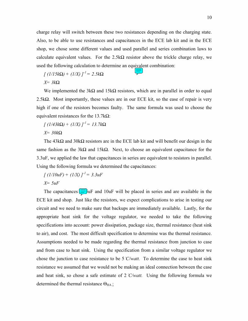
charge relay will switch between these two resistances depending on the charging state.
Also, to be able to use resistances and capacitances in the ECE lab kit and in the ECE
shop, we chose some different values and used parallel and series combination laws to
calculate equivalent values. For the 2.5kΩ resistor above the trickle charge relay, we
used the following calculation to determine an equivalent combination:
[ (1/15kΩ) + (1/X) ]-1 = 2.5kΩ
X= 3kΩ
We implemented the 3kΩ and 15kΩ resistors, which are in parallel in order to equal
2.5kΩ. Most importantly, these values are in our ECE kit, so the ease of repair is very
high if one of the resistors becomes faulty. The same formula was used to choose the
equivalent resistances for the 13.7kΩ:
[ (1/43kΩ) + (1/X) ]-1 = 13.7kΩ
X= 30kΩ
The 43kΩ and 30kΩ resistors are in the ECE lab kit and will benefit our design in the
same fashion as the 3kΩ and 15kΩ. Next, to choose an equivalent capacitance for the
3.3uF, we applied the law that capacitances in series are equivalent to resistors in parallel.
Using the following formula we determined the capacitances:
[ (1/10uF) + (1/X) ]-1 = 3.3uF
X= 5uF
The capacitances of 5uF and 10uF will be placed in series and are available in the
ECE kit and shop. Just like the resistors, we expect complications to arise in testing our
circuit and we need to make sure that backups are immediately available. Lastly, for the
appropriate heat sink for the voltage regulator, we needed to take the following
specifications into account: power dissipation, package size, thermal resistance (heat sink
to air), and cost. The most difficult specification to determine was the thermal resistance.
Assumptions needed to be made regarding the thermal resistance from junction to case
and from case to heat sink. Using the specification from a similar voltage regulator we
chose the junction to case resistance to be 5 C/watt. To determine the case to heat sink
resistance we assumed that we would not be making an ideal connection between the case
and heat sink, so chose a safe estimate of 2 C/watt. Using the following formula we
determined the thermal resistance ΘHA :

11
Pd = Tj – Ta 10 watts = 150C - 30C
ΘJC + ΘCH + ΘHA 5 C/watt + 2 C/watt + ΘHA
ΘHA < 5 C/watt
To be in a safe range in order to not damage the regulator, we found a heat sink with a
4 C/watt thermal resistance. The package size of the regulator is TO-220 so the heat sink
package is TO-220. With these two specifications we were able to find a heat sink with
suitable power dissipation, 15 watts. Our regulator will not be dissipating more than 10
watts so this value is fine. The lowest cost for a heat sink that matches these criteria is
$3.21, which is not excessive but not very cost-effective. This is a forced tradeoff we
decided to make.
3.3. Overcharge Protection Circuit
The overcharge protection circuit prevents possible damage to the battery by
switching the charger to charge the battery at a lower charging voltage when it is sensed
that the battery is already mostly charged. The battery will naturally draw less and less
current as it replenishes its charge. Therefore, the current flowing from the charger to the
battery is a good indication of the amount of charge stored in the battery. Figure 5 shows
the circuit we have designed to sense and process this information.

12
Figure 5: The Overcharge Protection Circuit
The circuit consists of three stages, each of which is crucial to its functionality. The
current flowing from the charging circuitry (labeled as Vreg) to the battery goes through
sensor resistor Rs, producing a voltage drop. This voltage, which is a positive difference
because of the new way we hooked the resistor up, is amplified by the difference
amplifier stage, which is configured by resistors R1 – R4. Because of the configuration
change we made, this amplifier now has a gain of 2. When the amplified voltage at the
output of the difference amplifier drops below the new threshold of 80 mV, the Schmitt
trigger, re-configured by resistors R5 and R6, will output a logic high of above 4.6 volts.
This voltage will activate the switching circuitry by being applied to the base of transistor
Q1. This will turn the transistor on, which will in turn draw current through the coil,
which will switch the relay to set the charging circuit to trickle-charge mode. The
addition of the normally open switch at the base of the coil provides an alternate path for
current to go through if the user of the charger decides to hook up another device to the
battery while it is charging. This switch, when closed, will activate the relay in the same

13
fashion as the automatic circuitry, preventing the battery from being overcharged by a
high voltage.
For precise details of the operation of the overcharge protection circuit, see Section
3.4 of the 4th report, our Overall Design Progress Report. The design changes made to
this circuit as of the publication of this report are certainly to our advantage. The re-
configuration of the difference amplifier and Schmitt-trigger stages absolutely had to be
done, since our previous configuration was based on faulty knowledge of the use of op-
amps. The addition of the toggle switch for hooking up a device to the battery while
charging is also a very important precaution, for the overcharge protection system was
not designed to compensate for additional current drawn by outside devices other than the
battery.
3.4. Casing
There was a variety of casing options available to choose from. Possibilities included
steel, aluminum, titanium, plastics, wood, and marble. After further research it was
realized that the most plausible and cost effective enclosure was plastic because it is
durable and lightweight. Some characteristics that needed to be accounted for besides
durability were temperature ranges, whether it is waterproof (if possible), and whether we
could drill holes and maintain structural integrity. We were able to do all of these
modifications with a plastic case, and most importantly, we could do them cheaply.
There are a variety of chemical compositions of plastics that result in different strengths
and appearances. For example, a nice transparent plastic box like the one in Figure 6
would allow for a more visually stunning product.
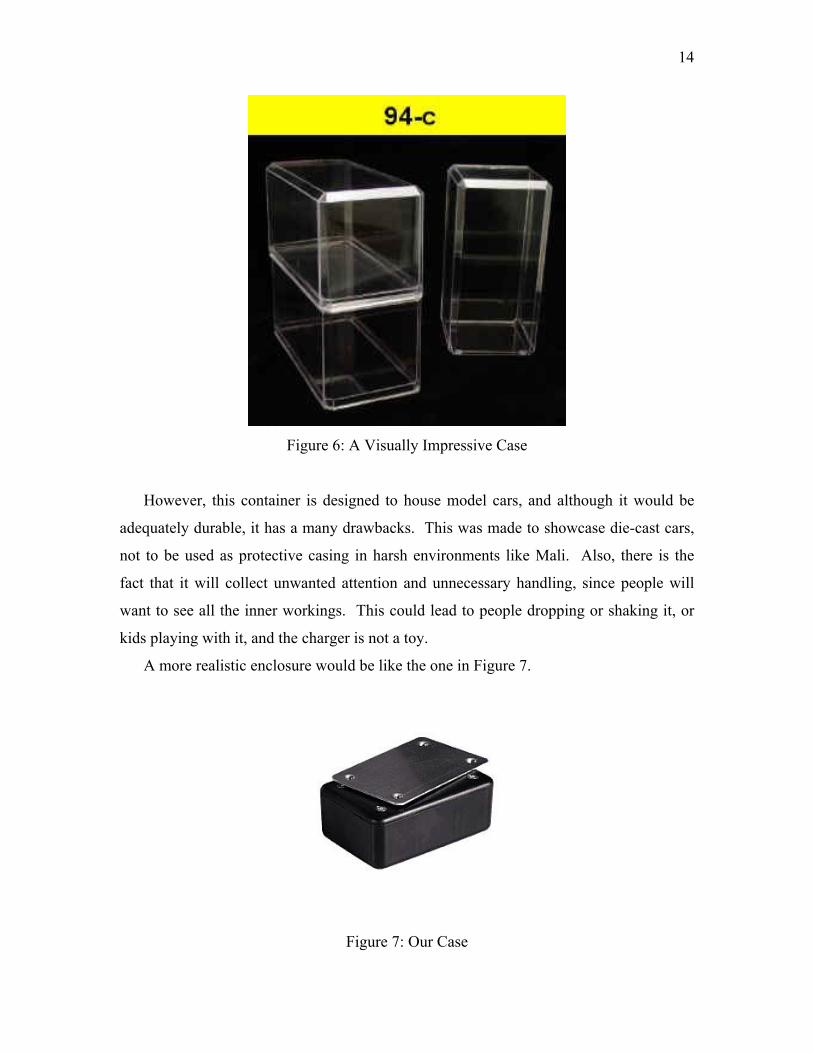
14
Figure 6: A Visually Impressive Case
However, this container is designed to house model cars, and although it would be
adequately durable, it has a many drawbacks. This was made to showcase die-cast cars,
not to be used as protective casing in harsh environments like Mali. Also, there is the
fact that it will collect unwanted attention and unnecessary handling, since people will
want to see all the inner workings. This could lead to people dropping or shaking it, or
kids playing with it, and the charger is not a toy.
A more realistic enclosure would be like the one in Figure 7.
Figure 7: Our Case
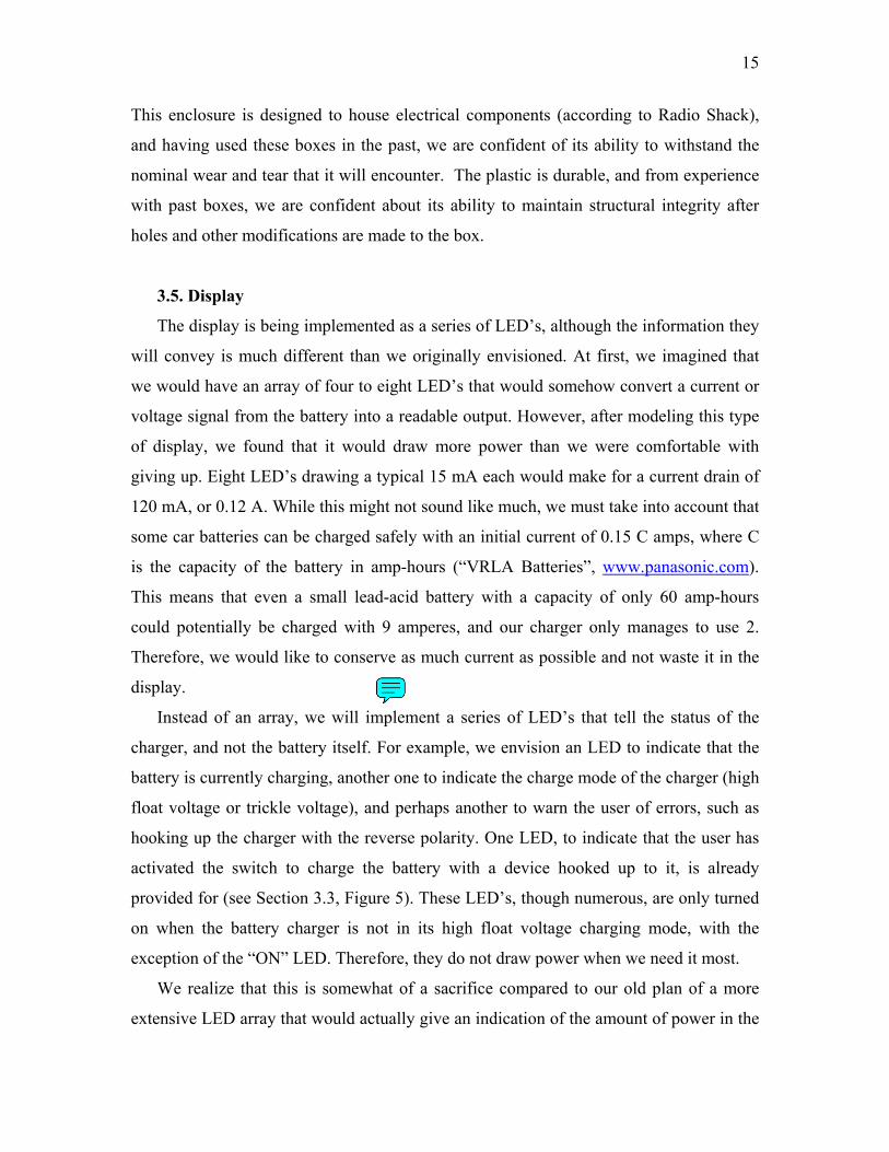
15
This enclosure is designed to house electrical components (according to Radio Shack),
and having used these boxes in the past, we are confident of its ability to withstand the
nominal wear and tear that it will encounter. The plastic is durable, and from experience
with past boxes, we are confident about its ability to maintain structural integrity after
holes and other modifications are made to the box.
3.5. Display
The display is being implemented as a series of LED’s, although the information they
will convey is much different than we originally envisioned. At first, we imagined that
we would have an array of four to eight LED’s that would somehow convert a current or
voltage signal from the battery into a readable output. However, after modeling this type
of display, we found that it would draw more power than we were comfortable with
giving up. Eight LED’s drawing a typical 15 mA each would make for a current drain of
120 mA, or 0.12 A. While this might not sound like much, we must take into account that
some car batteries can be charged safely with an initial current of 0.15 C amps, where C
is the capacity of the battery in amp-hours (“VRLA Batteries”, www.panasonic.com).
This means that even a small lead-acid battery with a capacity of only 60 amp-hours
could potentially be charged with 9 amperes, and our charger only manages to use 2.
Therefore, we would like to conserve as much current as possible and not waste it in the
display.
Instead of an array, we will implement a series of LED’s that tell the status of the
charger, and not the battery itself. For example, we envision an LED to indicate that the
battery is currently charging, another one to indicate the charge mode of the charger (high
float voltage or trickle voltage), and perhaps another to warn the user of errors, such as
hooking up the charger with the reverse polarity. One LED, to indicate that the user has
activated the switch to charge the battery with a device hooked up to it, is already
provided for (see Section 3.3, Figure 5). These LED’s, though numerous, are only turned
on when the battery charger is not in its high float voltage charging mode, with the
exception of the “ON” LED. Therefore, they do not draw power when we need it most.
We realize that this is somewhat of a sacrifice compared to our old plan of a more
extensive LED array that would actually give an indication of the amount of power in the

16
battery, but we feel that it is well worth it. The customer specification for a charge
indicating display was determined at the beginning of the project to have much lower
importance than the customer specifications of low cost and high efficiency (refer to
Progress Report #2). Thus, to sacrifice some of the functionality of the display in an
effort to cut cost and especially raise efficiency is a wise move from the overall
perspective of the project.

17
4. Revised Project Schedule
We are very satisfied with our progress thus far on this project, and are right on
schedule to have a working prototype by December 17, 2003. We have updated our Gantt
chart, shown in Figure 8, to reflect our progress so far and to be more flexible with the
way we get things accomplished. There are specific start dates for each sub-project, but
our contingency plan provides for them all to be done by December 14, 2003.
Wednesday
Thursday
Friday
Saturday
Sunday
Monday
Tuesday
Wednesday
Thursday
Friday
Saturday
Sunday
Monday
Tuesday
Wednesday
Thursday
Friday
Saturday
Sunday
Monday
Tuesday
Wednesday
Thursday
Friday
Saturday
Sunday
Monday
Tuesday
Wednesday
Thursday
Friday
Saturday
Sunday
Monday
Tuesday
Wednesday
Thursday
TASK Person(s) Responsible
########
########
########
########
########
########
########
########
########
########
########
########
########
########
########
########
########
########
########
12/1/2003
12/2/2003
12/3/2003
12/4/2003
12/5/2003
12/6/2003
12/7/2003
12/8/2003
12/9/2003
########
########
########
########
########
########
########
########
########
ResearchAC/DC Conversion Mike ---- ---- ---- ---- ---- ---- XTransformers Mike ---- ---- ---- ---- ---- ---- XRegulators Anthony ---- ---- ---- ---- ---- XAmplification Anthony ---- ---- ---- ---- ---- XDC/DC Conversion Pete ---- ---- ---- ---- ---- XSensors Anthony ---- ---- ---- ---- XLED Arrays Anthony ---- ---- XCasing Mike ---- ---- XSurge Protection Pete ---- ---- ---- ---- ---- XCooling Pete ---- ---- ---- XBatteries Everyone ---- ---- ---- ---- ---- XOverflow Protection Pete ---- ---- ---- ---- ---- ---- X
DesignAC/DC Conversion Mike & Anthony ---- ---- ---- ---- XSurge Protection Mike ---- ---- XRegulator Anthony ---- ---- ---- ---- ---- XOverflow Protection Pete ---- ---- ---- ---- ---- ---- XDC/DC Conversion Pete & Mike ---- ---- ---- ---- ---- XLED Arrays Anthony ---- XCooling Pete ---- XUser Interface Anthony ---- ----Completion Everyone ---- X
ConstructionOrder Parts Everyone XAC/DC converter Mike & Anthony ---- ---- ---- ----Ampflication Pete & Anthony ---- ---- ---- ----Regulation Pete & Anthony ---- ---- ---- ----DC/DC Converter Pete & Mike ---- ---- ---- ----Surge Protection Mike ---- ---- ---- ----LED Array Anthony ----I/O hardware EveryoneCooling Pete ----User interface Everyone ----Integration Everyone ----Casing MikeCompletion Everyone
Troubleshooting &TestingAC/DC converter EveryoneAmpflication EveryoneRegulation EveryoneDC/DC Converter EveryoneSurge Protection EveryoneLED Array EveryoneI/O hardware EveryoneCooling EveryoneIntegration Everyone
Final ReportWrite report EveryoneWrite Presentation EveryonePresent Everyone
KEY Planned --- Currently Working OnContingency X Date CompletedThanksgving
Figure 8: Our updated Gantt Chart
As our Gantt chart indicates, we are presently in the construction phase. With the
exceptions of a heat sink and a transient voltage suppressor, all of our parts are ready for

18
prototyping. Our goal is to complete the construction phase by this Sunday, but this
deadline may be pushed up a couple days depending on when our late parts come in.
Because we are planning for many problems to arise in testing, we comfortably allotted
all of next week to test and troubleshoot. If parts that are available through ordering-only
happen to become damaged in the testing process, then we will certainly be experiencing
EE2799 “crunch time” to the fullest extent. As indicated in our chart, we will all be
active in the testing and troubleshooting process next week. It is our contention that
problems will be solved more practically and quickly with three brains at a lab bench,
instead of one or two. The last three days of school before the final report and
presentation are due will be spent composing our final report. We have found that the
ideal process to finishing a report is to have all three partners working at computers next
to each other with one member designated with the task of putting all the parts together
(Anthony). This process results in expeditiously completing reports with high quality
content.

19
5. Conclusion
This report has enlightened the reader as to all of the progress we have made since
Progress Report 4 was submitted almost 2 weeks ago. There are a good amount of design
changes that we made at the circuit level of construction, but from a top-level, subsystem
perspective, our design has not changed. We still feel that our overall scheme for
implementing the charger is well thought-out and a solid design. In addition to the
changes made to the existing circuits, we have developed ideas of how to implement the
remaining support sub-modules, such as cooling, casing, and the display. We believe the
design process is working out well for us, and as our revised Gantt chart shows, we have
progressed according to plan.

20
6. References
“Battery.” http://www.partsamerica.com , 11/21/03.
“Bridge Rectifier.” http://rocky.digikey.com/WebLib/Diodes_Inc/Web%20Data/rs401l-
rs407l.pdf , 11/20/03.
“Charging Batteries.” http://www.cloudelectric.com/generic.html , 11/20/03.
“Digi-Key.” www.digikey.com, 11/1/03.
“Rechargeable Sealed Lead-Acid Batteries.” http://www.power-sonic.com , 11/21/03.
“Relays.” http://www.itee.uq.edu.au/~engg1030/lectures/1perpage/lect12.pdf , 11/22/03.
Sedra, Adel S. and Kenneth C. Smith. Microelectronic Circuits. New York: Oxford
University Press, 1998.
“TLV Family of Operational Amplifiers.” http://focus.ti.com/lit/ds/slos220i/slos220i.pdf ,
11/20/03.
“Transient Voltage Suppressor Diodes.”
http://www.fagorelectronica.com/semi/pdf/transien.pdf , 11/21/03.
“VRLA Batteries.” http://www.panasonic.com , 11/21/03.
“W58 Series Thermal Circuit Breaker.”
http://www.pandbrelays.com/datasheets/Circuit_Breakers/W58_DS.pdf ,
11/22/03.