ultra-wideband direct conversion receivers for satellite … · 2007-06-19 · 1 ultra-wideband...
TRANSCRIPT
1
Ultra-Wideband Direct Conversion Receivers for Satellite On-Board Processing�
– System Analysis and Digital Error Compensation –
Heiko Kopmann* and Heinz G. Göckler† Ruhr-Universität Bochum, Universitätsstr. 150, Bochum, D-44780, Germany
In this contribution, a direct conversion receiver (DCR), zero IF or homodyne receiver applying in-phase/quadrature (I/Q) sampling has been revisited in conjunction with digital error compensation. Contrary to common practice, our main interest is focused on the inves-tigation of performance degradation in conjunction with the processing of ultra-wideband frequency division multiplex (FDM) signals. To this end, all potential error sources have been identified and introduced into a comprehensive error model. This error model com-prises path individual DC-offsets, gain, phase and time delay mismatch, bidirectional crosstalk between the input ports of the down-converters, quantisation and overflow satura-tion (clipping) errors, as well as time jitter due to sample-and-hold circuits and clock genera-tor. For all of these error sources an exact error analysis has been carried out. Furthermore, a typical error scenario taken from an ultra-wideband application in satellite communica-tions has been used to demonstrate the overall performance degradation as a result of the combination of these error contributions. For this application, the major degradations are caused by DC-offsets that heavily impair the channel centred at zero frequency, branch time delay difference that are most pronounced in edge channels, and gain mismatch. Each of these three error sources introduces, on its own, a performance degradation such that error compensation measures are compulsive. In contrast, all other error contributions are of mi-nor influence. To reduce degradation, blind digital error compensation methods have been investigated to estimate and compensate the most important errors. In particular, a novel approach to compensate for I/Q time delay mismatch has been developed. The combination of this novel delay mismatch compensation method with known DC-offset, gain, and phase compensation techniques results in highly improved signal to noise and distortion ratio (SNDR). This enhancement due to digital error compensation will be demonstrated by simu-lation by applying the above ultra-wideband scenario.
I. Introduction N modern ultra-wideband receivers, e.g. of satellite communication systems and software defined radio, the inter-face between analogue and digital signal processing is more and more shifted towards the receiver's front end (an-
tenna, optical/electrical interface, etc.), to make use of the advantages (robustness, volume, reproducibility, etc.) of digital signal processing. For these ultra-wideband and high-speed applications – e.g. of bandwidths of more than 1 GHz – present-day state-of-the-art conventional analogue-to-digital converters (ADC) are either too slow, or re-solve the signal to be quantised too coarsely1,2. Therefore, it is a challenging task to develop extremely fast and yet precise enough ultra-wideband front-end analogue-to-digital interfaces (ADI).
Based on a parallel connection of several ADC there exist four basic approaches: Multiple concurrent ADI (MC-ADI) 3-7, time-interleaved ADI (TI-ADI) 3,5-11, hybrid ADI (H-ADI) 3,5-7 and, in conjunction with a direct conversion receiver (DCR), the A-to-D conversion of a complex-valued signal (I/Q sampling) 3,12. By the MC-ADI approach the
� This work has partly been supported by Tesat-Spacecom GmbH, Backnang, Germany and ESA / ESTEC, Noordwijk, The Netherlands. * Former Ph.D. Candidate with Digital Signal Processing Group. † Professor, Head of Digital Signal Processing Group (email: [email protected]).
I
2
resolution is increased. Here, all ADC of the interface are controlled by the same clock. The improved output signal of the MC-ADI is obtained as arithmetic mean of each set of concurrent output samples of all ADC in parallel. Con-trary, the TI-ADI allows for a higher sampling rate. Here, a parallel connection of slower time-interleaved ADC is used. The H-ADI combines the TI- and MC-ADI approaches in such a manner that each ADC of the TI approach is replaced with an MC-ADI. Finally, using a DCR, the A-to-D conversion of the complex envelope (i.e. baseband signal) is performed by two synchronously sampling ADC – or alternatively by two of the former ADI in parallel – where both the ADC and ADI, respectively, are operated at half the sampling frequency (due to sampling of com-plex-valued signals).
The focus of this paper is set onto the DCR applying I/Q sampling. Firstly, the ideal operation of a DCR is re-called in the following section. In the subsequent section a comprehensive parametric error model of the ultra-wideband DCR is developed. This error model comprises path individual DC-offsets, gain, phase and time delay mismatch, bidirectional crosstalk between the input ports of the down-converters, quantisation and overflow satura-tion (clipping) errors, as well as time jitter due to sample-and-hold circuits and clock generator. In section IV, the impact of all of these system parameters is analysed by analytic evaluation. This system analysis is based on the recently published analysis in Ref. 12, which is extended by time jitter.
Some of the above mentioned error sources introduce an overall degradation such that error compensation meas-ures are mandatory. To reduce this degradation, in section V, blind digital error compensation methods have been investigated to estimate and compensate DC-offsets, different gains, phases, and time delays in the I and Q paths. In particular, a novel approach to compensate for I/Q time delay mismatch has been developed, in which the unknown time delay difference is digitally estimated during uninterrupted system operation, without the need of any training or calibration signal. This novel approach to be reported is applied to FDM signals, being composed of quadrature phase shift keying (QPSK) sub-signals; however, it can easily be extended to higher level digital modulation schemes. Furthermore, the combination of the novel delay mismatch compensation method with known DC-offset, gain, and phase compensation techniques13,14 is investigated, to get the optimum sequential order of the various error compensators. The enhancement due to digital error compensation will be demonstrated by simulations by applying typical error scenarios, taken from ultra-wideband satellite on-board processing applications with overall FDM bandwidths of 150 MHz and 1 GHz, respectively.
II. The Ideal Direct Conversion Receiver Fig. 1 shows the block diagram of the ideal DCR from signal splitting up to the ADI. The input signal x(t) is
branched into two paths. In one path, the so-called in-phase or I-path, the signal is mixed with a sinusoidal carrier derived from a local oscillator (LO) of frequency fO. The signal in the so-called quadrature or Q-path is mixed with the LO carrier of the same frequency but with 90° phase offset. The resulting signals are band-limited by an anti-aliasing filter and A-to-D converted for subsequent digital signal processing.
In the following, we describe the DCR principle by assuming an arbitrarily modulated input signal starting with
^ ` ^ ` C C C C
*j[ ( )] j j j1( ) Re ( )e Re ( )e ( )e ( )e
2t t t t tx t A t x t x t x tZ M Z Z Z� �ª º �¬ ¼� � � , (1)
where ZC = 2SfC represents the carrier frequency, )(~* tx the complex conjugate of )(~ tx , and
j ( )( ) ( )e , ( ) 0 tx t A t A t tM ! �� (2)
the complex envelope of x(t) with
0)(j~ ZX�
, for CB 2 ZSZZ �� ! B , (3)
where )(j~
ZX�
is the FOURIER transform (FT) of )(~ tx and B the usable bandwidth. Note that complex-valued signals
and Fourier transforms thereof are indicated by underlining. For the description of the DCR receiver, the I and Q signals are regarded as the real and imaginary components of a complex-valued signal corresponding to the complex envelope (2). In the same way, the two real-valued LO-carriers are replaced with one complex-valued carrier:

3
Figure 1. Ideal DCR including ADI
� � � � OjO Ocos jsin e tt t ZZ Z �� . (4)
Thus, the output signal of the complex-valued mixer is given by
� � � � C O C O*j j
M
1( ) ( )e ( )e
2t ty t x t x tZ Z Z Z� � �ª º �¬ ¼� � (5)
After low-pass filtering (to remove the sum-frequency components about ZC + ZO) and sampling at tk = t0+kT, where T = 1/fS is the sampling period, the discrete-time output signal
� � C O
ji q id
1( ) ( ) j ( ) ( ) ( )e
2kt
k k k k ky t y t y t y t x t Z Z� � � (6)
is obtained. If the LO frequency fO is equal to the carrier frequency fC, the output signal )( kty is equal to the com-
plex envelope )(~ktx scaled by ½.
III. Error Model In this section we introduce the comprehensive DCR error model, as depicted in Fig. 2. Here, all relevant gain
and phase transfer functions of hardwired and undesired crosstalk connections in conjunction with corresponding offsets are characterised by illustrative parameters. For worst case error analysis all these parameters are assumed independent of time and frequency. In the error model3,12 the following parameters generally deviating from their nominal values are considered:
x DC offsets oi and oq introduced by the mixers and the ADCs in the I and Q paths, respectively. x Gain mismatch gE introduced by different gains of the signal splitter, the mixers, the low-pass filters,
and the ADCs in the I and Q paths. Obviously, the gain differences in the I and Q paths are caused by tolerance problems of the analogue electronic devices.
x Phase error ME, which is introduced by the signal splitter and the local oscillator (LO) in conjunction with mixing. Different phase delays due to non-identical lengths of the respective wire connections are also contained in this parameter. Note that the above basic assumption of frequency-independent phase functions is (approximately) valid only for small relative bandwidths; for our worst case analysis, how-ever, this assumption can be taken for granted.

4
Figure 2. Error Model of DCR including ADI
x Time delay mismatch WE introduced by different group delays of the low-pass anti-aliasing filters and different aperture times of the ADCs in the I and Q paths.
x Time jitter Ws,i(t) and Ws,q(t) in the I and Q paths, respectively, introduced by the ADCs and the clock generator.
x Bidirectional crosstalk between the mixer input ports characterised by the self-explaining parameters c’OS,i, M’OS,i, c’OS,q, and M’OS,q as well as c’SO,i, MSO,i, c’SO,q, and MSO,q, respectively. Again, c represents the magnitude and M the phase, and the indices i and q denote the in-phase and quadrature components, respectively. These errors are due to capacitive and inductive cross coupling within the circuit layout and wiring as well as junction capacitances of certain transistors.
x Quantisation and saturation (clipping) errors with the non-linear parts ei(tk) (I path) and eq(tk) (Q path), as well as the linear parts of the clipper transfer functions, which are represented by the equivalent gains G(pf,i) and G(pf,q), respectively.
Note that, in addition, it is assumed that the frequency offset of the LO is small (ZO §�ZC) and that the narrow
band assumption (ZB << ZC) is valid. Errors that merely cause an amplification, phase shift and/or delay of the com-plex signal rather than of its components, are combined to the modified RF input signal x’( t) and its complex enve-lope ’( )kx t� , respectively. Details are published in Ref. 3 or, without time jitter, in Ref. 12.
IV. Error Analysis In this section, the impact of the main mismatch errors3,12 originating from the analogue modules of the DCR
comprising the ADI �QDPHO\�'&-offsets, gain, phase, and time delay deviations �RQ�WKH�VSHFWUXP�RI�WKH�LQWHULP�analogue DCR output signal is investigated by evaluating the error model introduced above. Note that quantisation, clipping, etc. are not considered, since the digital error compensation to be reported only aims at reducing the above mismatch errors. To this end, firstly, the I and Q components of the analogue complex-valued DCR output signal are calculated in the time domain (Fig. 2):
^ ` ^ `*’ ’ ’i i iid id id
1( ) Re ( ) ( ) ( )
2y t y t o y t y t oª º � � �¬ ¼ (7)

5
and ^ ` ^ `E E E*’ ’ ’j j jE
q E E q E E qid id id( ) Im ( )e ( )e ( ) e
2 j
gy t g y t o y t y t oM M MW W W� � ª º � � � � � �¬ ¼ , (8)
respectively, where similarly to Eq. (6): � � C O’ j
id
1( ) ’( )e
2kt
k ky t x t Z Z� � . (9)
The I and Q components of Eq. (7) and Eq. (8) are subjected to the FOURIER transform:
*’ ’
i iid id
1( j ) ( j ) ( j ) 2 ( )
2Y Y Y oZ Z Z S G Z ½ª º � � �® ¾« »¬ ¼¯ ¿
�� � �
(10)
and � � � �E E E E
*’ ’j jEq qid id( j ) ( j )e ( j ) e 2 ( )
2 j
gY Y Y oZW M ZW M
Z Z Z S G Z� � � � ½ª º � � �® ¾« »¬ ¼¯ ¿�� � �
, (11)
respectively. For convenience, these two baseband components are combined to the spectrum of the complex-valued output signal:
� �� � � �� � � �E E E E
*’ ’j jE E i qid id
1 1( j ) 1 e ( j ) 1 e ( j ) 2 j ( )
2 2Y g Y g Y o oZW M ZW MZ Z Z S G Z� � � � ª º � � � � � �« »¬ ¼
�� � �
. (12)
Obviously, the channel containing zero frequency is impaired by the DC-offsets (3rd term). Additionally, the usable spectrum (1st term) is superimposed by an image spectrum (2nd term), which is caused by different gains, phases, and time delays in the I and Q paths.
Considering only the time delay difference WE, Eq. (12) simplifies to
E E *j j’ ’E E2 2
id id( j ) e cos ( j ) je sin ( j )2 2
Y Y YZW ZWZW ZWZ Z Z� �§ · § · ª º � �¨ ¸ ¨ ¸ « »¬ ¼© ¹ © ¹
� � �
. (13)
Under the assumption | fWE | ��½, the magnitude of the image spectrum (2nd term) increases with the absolute fre-quency | f |, whereas the magnitude of the usable spectrum (1st term) decreases. Therefore, the higher the absolute frequency | f |, the lower the signal to noise and distortion ratio (SNDR).
V. Digital Error Compensation To reduce the degradation due to I/Q mismatch, in this section digital methods for blind estimation and compen-
sation of DC-offsets, gain, phase, and time delay errors are presented. In particular, a novel approach to compensate for I/Q time delay mismatch is developed. Furthermore, the combination of this novel delay mismatch compensation method with known DC-offset, gain, and phase compensation techniques13,14 is investigated.
A. Compensation of DC-Offsets For convenience, we assume the usable component of the input signal to have no DC component (otherwise refer
to Ref. 3). Hence, a suitable method for DC-offset compensation is to subtract an estimated value of the DC-offset, which is extracted from the ADC output signal by long term averaging13,14, as shown in Fig. 3. The performance of this approach depends, in addition to the number of observations Bo, mainly on the power spectral density (PSD) of the ADC input signal at zero frequency3. The higher Bo and the lower the PSD of the ADC input signal at zero fre-quency, the lower the variance of the DC-offset estimator. Under certain mild, generally satisfied assumptions, the convergence of the estimator has been proven in Ref. 3.
For a sufficiently small standard deviation of the estimator, an extreme high number Bo of observations may be necessary. Therefore, a sliding calculation of the mean value is hardly to realise. For this reason, a blockwise estima-tion is preferable, where averaging is performed recursively, as shown in Fig. 4. The value in the register is used to compensate the ADC output signal (Fig. 3). The DC-offsets, which are estimated from one block of samples, are used for compensation of the next block. The DC-offset estimator is thus updated during operation.

6
Figure 5. Compensation of Gain Mismatch by Averaging of Signal Magnitudes using a Reference
Figure 3. DC-Offset Compensation
by Long Term Averaging Figure 4. Long Term Averaging by Recursive Block Processing
B. Compensation of Gain Mismatch In this subsection, a known gain mismatch compensation technique is recalled according to Ref. 13 and Ref. 14.
This method is based on the arithmetic means of the magnitudes of the ADC output signals. Again, Bg is the number of observations. The received long term averages of the rectified path signals are divided to produce the compensa-tion factor, as shown in Fig. 5, where one path is used as a reference. Hence, for compensation of gain mismatch, the signal in the other path is multiplied by the obtained compensation factor.
The calculation of the required arithmetic mean is performed in the same way, as shown in Fig. 4 for the DC-offset compensation. Since two arithmetic means over Bg samples are divided, scaling by 1/Bg is not necessary. The variance of the gain mismatch estimator depends, in addition to the number of observations Bg, on the DCR input signal. For a reliable operation, an I/Q balancing of the power of the input signal is necessary. Otherwise, a gain mismatch is estimated even if gain mismatch does not exist. Hence, estimated values should be discarded, if the dif-ference between the two arithmetic means is too high. In practical applications, the condition of I/Q balancing of the input power is usually satisfied very well. In Ref. 3, the convergence of the estimator has been proven for zero DC-offset (being equivalent to its compensation in front of the gain mismatch compensator).
Note that this method can easily be modified in such a manner that the estimator is independent of DC-offsets and their compensations, respectively. To this end, the signals are differentiated to eliminate the DC components, before the arithmetic means are calculated14.
C. Compensation of Phase Error In the following, an approach to the compensation of the phase error via coordinate transformation is presented14.
Here, the phase error is mapped onto a gain error, which is subsequently compensated for by the gain mismatch compensation technique of Fig. 5. To this end, the complex-valued DCR signal is rotated by ±45°:

7
Figure 6. Compensation of Phase Error via Coordinate Rotation and Gain Mismatch Compensation
’i i q
1( ) ( ) ( )
2k k ky t y t y tª º ¬ ¼# and ’
q q i
1( ) ( ) ( )
2k k ky t y t y tª º r¬ ¼ , (14)
where, for simplification, the superfluous scaling by 1 2 is subsequently discarded by replacing (14) with:
"i i q( ) ( ) ( )k k ky t y t y t # and "
q q i( ) ( ) ( )k k ky t y t y t r . (15)
As a result, any I/Q phase mismatch is, thus, detected as a gain mismatch of the rotated signal, provided that the true gain mismatch of the original signal has been compensated for beforehand. Fig. 6 shows the simplified phase rota-tion (left block), and the gain mismatch compensation according to Fig. 5 (right block of Fig. 6).
The (ideal) complex envelope ’id
( )ky t is, as a result of phase error compensation according to Fig. 6, subjected to
a fixed amplification by a sine-function and to a constant phase rotation by an exponential factor:
Ej
’ 4 2E
id( ) 2sin ( ) e
4 2k ky t y tMS
M
MS § ·r �¨ ¸© ¹§ ·| r¨ ¸© ¹ for E 2
SM � . (16)
It should be noted that both deviations are time-independent, since E .constM Hence, for most applications (e.g. in
communications) the impact of these signal manipulations is irrelevant.
Under certain mild, generally satisfied assumptions, the convergence of this compensation method is guaranteed, if the DC-offsets, gain, and time delay mismatch errors have been compensated before3. Note that this method can, in the same way as the gain mismatch compensation technique, be modified to be independent of the DC-offsets14.
D. Compensation of Time Delay Difference In this section, a novel approach to the compensation of time delay mismatch is developed applying the results of
the error analysis of section IV: The unknown time delay difference is digitally estimated during uninterrupted sys-tem operation, and without the need of any training or calibration signal. This novel approach is applied to FDM signals, being composed of QPSK modulated sub-signals with a phase offset of 45°; however, it is easily extended to higher level digital modulation schemes, e.g. to any M-PSK or digital quadrature amplitude modulation (QAM).
As it can be deduced from Eq. (13), the baseband signal space representation of a QPSK modulated signal is compressed and rotated, respectively, by
C, E C, Ecos and2 2c cgW W
Z W Z WI � (17a,b)

8
Figure 7. Compensation of Time Delay Mismatch for FDM Signals with QPSK Modulated Sub Signals with a Phase Offset of 45°
in dependence of the time delay difference WE, where fC,c is the baseband centre frequency of the considered channel. In addition, due to noise and an image spectrum, respectively, where the latter is caused (amongst other things) by group delay mismatch errors, the nominal symbols appear as clouds in the signal space. However, by long term av-eraging the foci of the locations of the symbols actually received as a result of group delay mismatch are estimated. By comparing these estimates of the received symbols with their nominal locations in the signal space, the rotation angle is determined. Consequently, from Eq. (17b) an estimator of the time delay difference is readily deduced:
E C,C,
ˆ2ˆ for 0c
c
WIW ZZ
� z (18)
Provided that, in case of QPSK modulated signals, the maximum undesired rotation induced by group delay mis-match does not exceed 45°, sensitivity and accuracy of the estimator (18) is highest in edge channels with maximum absolute centre frequency. Due to its lower sensitivity, the alternative estimator based on Eq. (17a) was discarded.
The associated block diagram is shown in Fig. 7: To compensate for the time delay difference, a fractional delay (FD) filter is inserted in the DCR Q-path. For an efficient realisation of the FD filter we use the FARROW struc-ture15,16, and the method to determine the associated coefficients is based on LAGRANGE interpolation15,17.
The actual time delay difference is estimated from the QPSK detector input signal of a suitably selected sub-band QPSK demodulator (preferably of an edge channel). To this end, these decider input signals are integrated over BW observations and, eventually, compared with the associated detected symbols, i.e. the ideally transmitted symbols.
By calculating the actual angle of the obtained phasors and their deviations from the nominal angles, an estimated
value of the time delay difference is obtained according to Eq. (18). Due to the recursive nature of this approach, this
value represents the difference to the preceding estimator. The details of time delay difference estimation can readily
be deduced from the corresponding block diagram in Fig. 7.

9
Figure 8. Optimum Sequential Order of Compensators
Table 1. Overview of the Influence of DC-offsets, Gain, Phase, and Time Delay Mismatch
on the Different Compensation Methods Compensation of … f(o) f(gE) f(ME) f(WE) DC-offsets Gain Mismatch (x) Phase Mismatch (x) x x Time Delay Difference (referring to estimation)
x x
At start-up of this group delay difference compensation method, high errors of time delay difference estimation are possible as a result of an initially high symbol error rate (SER) in addition to the impact of not yet reduced gain and phase mismatch. If the SER is smaller than 50% (corresponding to the above given maximally allowed angle of ±45°), a correct trend of the estimator is guaranteed, which gradually yields a smaller SER step by step. Note that, due to non-ideal estimation with BW < ��DQG�GXH�UHDO�)'�ILltering with the finite interpolation order n < ���LQ�SUDctice the convergence threshold of SER is somewhat smaller than 50%.
Concluding, it should be mentioned that some simplifications are possible: i) Instead of using all four (nominal) symbols of a QPSK signal, any one of these may be used exclusively, ii ) The inverse tangent (arctan) function of the time delay estimation algorithm of Fig. 7 can be substituted by its argument, if the post-subtraction of S/4 is replaced with a pre-rotation of the complex-valued signal at the output port of the 6-Block by �45°; this operation can sim-ply be realized according to Eq. (15). For more details refer to Ref. 3.
E. Optimum Sequential Order of Compensators In this subsection, the combination of the presented compensation techniques is investigated to find out the op-
timum sequential order of the various error compensators. To this end, the results of the last subsections are summa-rised in Table 1, in order to give a survey of the interdependence of the four different mismatch compensation meth-ods used. Note that the dependence on the DC-offsets is set in parentheses since, by use of differentiators, the impact of DC-offset on the other compensators can be removed. By evaluating of Table 1, the optimum sequential order readily follows, as shown in Fig. 8. Further details are published in Ref. 3.
VI. Simulation Results In order to demonstrate the potential of the presented combined mismatch error compensation techniques with
the optimum sequential order of the individual methods according to Fig. 8, we present simulation results for two typical scenarios – ideal QPSK demodulation provided.
Scenario 1 Firstly, we choose an uncorrupted FDM input signal (SNDRx �����EHLQJ�FRPSRVHG�RI� ILYH�436.�PRGXODWHG�
sub-signals (phase offset: 45°) with identical signal power and the following channel allocations: fC,c = (c-3)Â���0+]�(c = 1, …, 5) and bandwidths: Bc = B = 30 MHz (bit rate: 44 Mbit/s; roll-off factor of the root NYQUIST filters: r = 0.35). We adopt the worst case error scenario listed in Table 2, which has also been used in Ref. 3. The sampling
10
Figure 9. Residual Error behind DC-Offset Compensator with Bo = 2
18 for I and Q Path Figure 10. Residual Error behind Gain Mismatch Compensator with Bg = 2
18
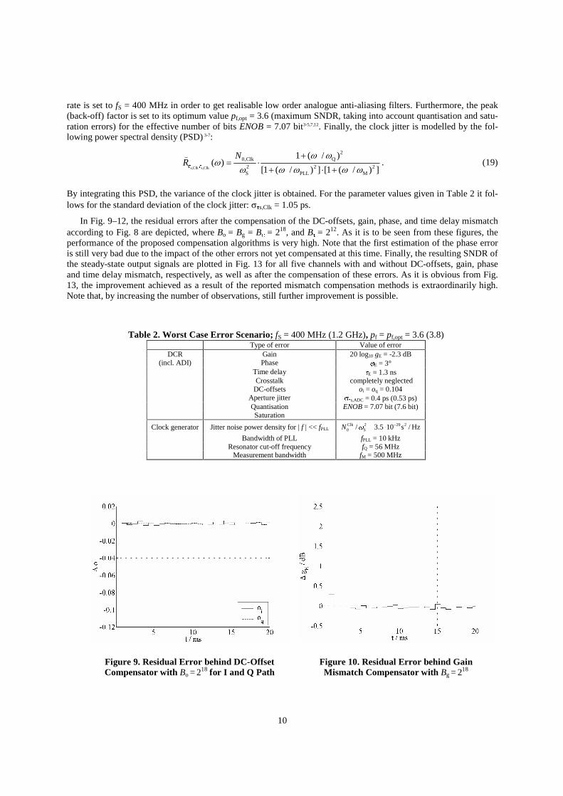
Table 2. Worst Case Error Scenario; fS = 400 MHz (1.2 GHz), pf = pf,opt = 3.6 (3.8)
Type of error Value of error DCR Gain 20 log10 gE = -2.3 dB
(incl. ADI) Phase ME = 3° Time delay WE = 1.3 ns Crosstalk completely neglected DC-offsets oi = oq = 0.104 Aperture jitter VWs,ADC = 0.4 ps (0.53 ps) Quantisation ENOB = 7.07 bit (7.6 bit) Saturation
Clock generator Jitter noise power density for | f | << fPLL Clk 2 29 20 S/ 3.5 10 s / HzN Z � �
Bandwidth of PLL fPLL = 10 kHz Resonator cut-off frequency fQ = 56 MHz Measurement bandwidth fM = 500 MHz
rate is set to fS = 400 MHz in order to get realisable low order analogue anti-aliasing filters. Furthermore, the peak (back-off) factor is set to its optimum value pf,opt = 3.6 (maximum SNDR, taking into account quantisation and satu-ration errors) for the effective number of bits ENOB = 7.07 bit3-5,7,12. Finally, the clock jitter is modelled by the fol-lowing power spectral density (PSD) 3-7:
s,Clk s,Clk
2Q0,Clk
2 2 2S PLL M
1 ( / )( )
[1 ( / ) ] [1 ( / ) ]
NRW W
Z ZZ
Z Z Z Z Z�
�� � �
�
. (19)
By integrating this PSD, the variance of the clock jitter is obtained. For the parameter values given in Table 2 it fol-lows for the standard deviation of the clock jitter: VWs,Clk = 1.05 ps.
In Fig. 9–12, the residual errors after the compensation of the DC-offsets, gain, phase, and time delay mismatch according to Fig. 8 are depicted, where Bo = Bg = BM = 218, and BW = 212. As it is to be seen from these figures, the performance of the proposed compensation algorithms is very high. Note that the first estimation of the phase error is still very bad due to the impact of the other errors not yet compensated at this time. Finally, the resulting SNDR of the steady-state output signals are plotted in Fig. 13 for all five channels with and without DC-offsets, gain, phase and time delay mismatch, respectively, as well as after the compensation of these errors. As it is obvious from Fig. 13, the improvement achieved as a result of the reported mismatch compensation methods is extraordinarily high. Note that, by increasing the number of observations, still further improvement is possible.

11
Figure 13. SNDR of the Output Signals: Scenario 1
Figure 14. SNDR of the Output Signals: Scenario 2 (SNDR < 0 in uncompensated channels with high absolute centre frequencies)
Figure 11. Residual Error behind Time Delay Mismatch Compensator with BW = 2
12 Figure 12. Residual Error behind Phase
Error Compensator with BM�= 218
Scenario 2
This scenario is characterised as follows3: fC = [-444 -324 0 324 444] MHz, B = [118 118 526 118 118] MHz (bit rate: [192 192 800 192 192] Mbit/s; r = [0.230 0.230 0.315 0.230 0.230]), and fS = 1.2 GHz. By using the worst case error values as given in Table 2, the SNDR of the output signals are obtained, as depicted in Fig. 14 for all channels with and without mismatch, as well as after its compensation. As it is to be seen from Fig. 14, mismatch error compensation again yields excellent improvement. It should be noted that, for channels with moderate and higher absolute centre frequencies, the SNDR is below zero in the uncompensated case (Fig. 14). Again, by increas-ing the number of observations, further improvement of SNDR is possible, leading to longer estimation times.
VII. Conclusion First, we recall the main results of the mismatch error analysis: i) The signal to noise and distortion ratio (SNDR)
of the DCR channel that contains zero frequency is extremely impaired by DC-offsets. ii ) The major SNDR degra-

12
dation in the remaining channels originates from an image spectrum, which is mainly caused by different gains, phases, and time delays in the I and Q paths. The impact of time delay mismatch is most pronounced in edge chan-nels, since the degradation due to delay mismatch depends on the absolute values of their centre frequencies. All these error sources introduce an overall degradation such that error compensation measures are mandatory. In con-trast, all other error contributions are of minor impact.
To reduce degradation, blind digital error compensation methods are investigated to estimate and compensate DC-offsets, gain, phase, and time delay mismatch. In particular, a novel approach to compensate for I/Q time delay mismatch is developed, in which the unknown time delay difference is digitally estimated during uninterrupted sys-tem operation, without the need of any training or calibration signal. This novel approach is applied to FDM signals, being composed of QPSK sub-signals; however, it is easily extended to higher level digital modulation schemes. The combination of the novel delay mismatch compensation method with known DC-offset, gain, and phase com-pensation techniques results in highly improved SNDR, optimum sequential order of the individual error compensa-tors provided. The enhancement due to digital error compensation is demonstrated by simulations of ultra-wideband satellite on-board processing applications with overall FDM bandwidths of 150 MHz and 1 GHz, respectively.
References 1 Walden, R.H., “Analog-to-Digital Converter Survey and Analysis,” IEEE J. Selected Areas in Commun., Vol. 17, No. 4,
1999, pp. 539-550. 2 Walden, R.H., “Performance Trends for Analog-to-Digital Converters,” IEEE Commun. Magazine, Vol. 37, No. 2,
1999, pp. 96-101. 3 Kopmann, H., “Breitbandige Analog/Digital-Schnittstellen – Systemanalyse und Beiträge zur digitalen Fehlerkompensa-
tion,” Ph.D. Dissertation, Digital Signal Processing Group, Ruhr-Universität Bochum, Germany, 2005. 4 Kopmann, H., Göckler H.G., and Abdulazim, M.N., “Analogue-to-Digital Conversion and Flexible FDM Demultiplex-
ing Algorithms for Digital On-Board Processing of Ultra-Wideband FDM Signals,” Proc. 8th Int. Workshop on Signal Processing for Space Commun., Catania, Italy, 2003, pp. 277-292.
5 Kopmann, H., “A Generalised Parametric Error Model of Ultra-Wideband Analogue-to-Digital Conversion,” Proc. 3rd Karlsruhe Workshop on Software Radios, Karlsruhe, Germany, 2004, pp. 101-110.
6 Kopmann, H., and Göckler, H.G., “Error Analysis of Ultra-Wideband Hybrid Analogue-to-Digital Conversion,” Proc. European Signal Processing Conf., Vienna, Austria, 2004, pp. 1091-1094.
7 Kopmann, H., “Comprehensive Model-Based Error Analysis of Multiple Concurrent, Time-Interleaved, and Hybrid Ul-tra-Wideband Analogue-to-Digital Conversion,” EURASIP J. Signal Processing, Vol. 84, No. 10, 2004, pp. 1837-1859.
8 Black, W.C., “High Speed CMOS A/D Conversion Techniques,” Ph.D. Dissertation, University of California, Berkeley, USA, 1980.
9 Black, W.C., and Hodges, D.A., “Time Interleaved Converter Arrays,” IEEE J. Solid-State Circuits, Vol. 15, No. 6, 1980, pp. 1022-1029.
10 Gustavsson, M., Wikner, J.J., and Tan, N.N., CMOS Data Converters for Communications, Kluwer, Dordrecht, 2000. 11 Vogel, C., “Comprehensive Error Analysis of Combined Channel Mismatch Effects in Time-Interleaved ADCs,” Proc.
IEEE Instrum. Meas. Technol. Conf., Colorado, USA, 2003, pp. 733-738. 12 Kopmann, H., and Göckler, H.G., “Comprehensive Error Analysis of Ultra-Wideband Direct Conversion Receivers,”
EURASIP J. Signal Processing, Vol. 83, No. 8, 2003, pp. 1597-1611. 13 Masterton, J., and Ramsdale, P.A., STC pic, London, GB, European Patent Application for “A Multi-Mode Radio Trans-
ceiver,” Docket No. EP 0 180 339 A2, filed 2 Oct. 1985. 14 Kluge, W., Jehring, F., and Krause, F.-M., Hagenuk GmbH, Kiel, Germany, German Patent Application for a “Verfahren
und Vorrichtung zur Korrektur der Phasen- und Amplitudenfehler bei direktmischenden Empfangseinrichtungen,” Docket No. DE 42 38 543 C1, filed 14 Nov. 1992.
15 Evangelista, G., “Zum Entwurf digitaler Systeme zur asynchronen Abtastratenumsetzung,” Ph.D. Dissertation, Digital Signal Processing Group, Ruhr-Universität Bochum, Germany, 2001.
16 Göckler, H.G., and Groth, A., Multiratensysteme, Schlembach, Wilburgstetten, 2004. 17 Schwarz, H.R., Numerische Mathematik, Teubner, Stuttgart, 1988.