trends in cmos digital design
TRANSCRIPT
Jan. 28, 2015 NIT-Patna: Foundation Day 2015 1
CMOS Digital Circuit DesignHow to Make Both Ends Meet?
Susanta SenInstitute of Radio Physics and Electronics
University of Calcutta
Jan. 28, 2015 NIT-Patna: Foundation Day 2015 2
Review of
MOS Transistor
Jan. 28, 2015 NIT-Patna: Foundation Day 2015 3
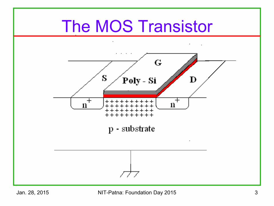
The MOS Transistor
Jan. 28, 2015 NIT-Patna: Foundation Day 2015 4
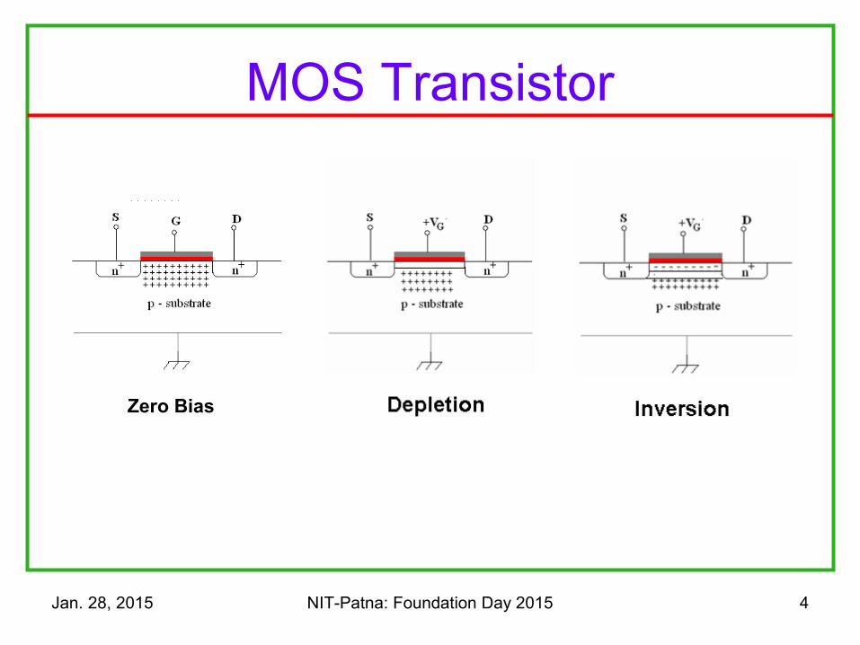
MOS Transistor
Zero Bias
Jan. 28, 2015 NIT-Patna: Foundation Day 2015 5
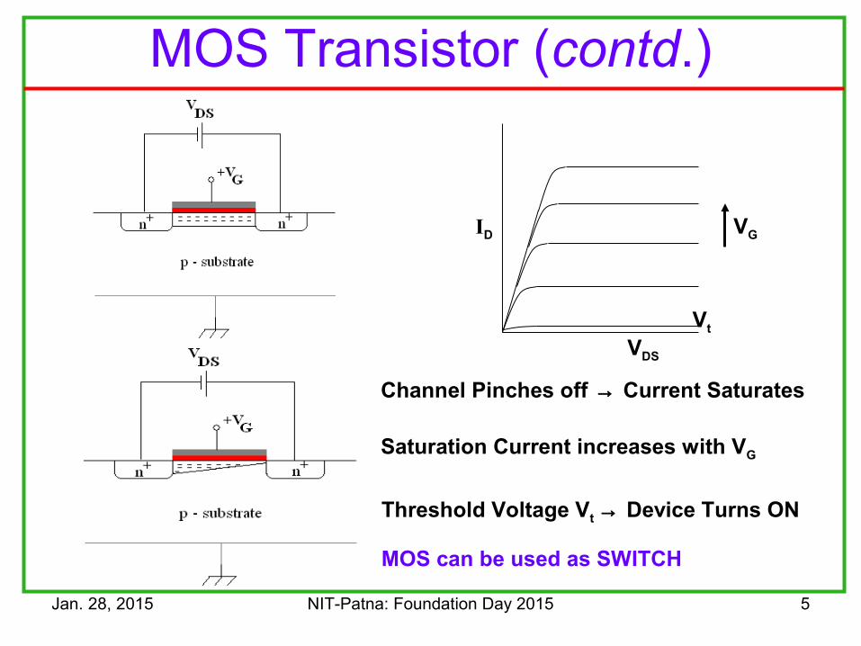
MOS Transistor (contd.)
VDS
ID
Channel Pinches off → Current Saturates
VG
Saturation Current increases with VG
Vt
Threshold Voltage Vt → Device Turns ON
MOS can be used as SWITCH
Jan. 28, 2015 NIT-Patna: Foundation Day 2015 6
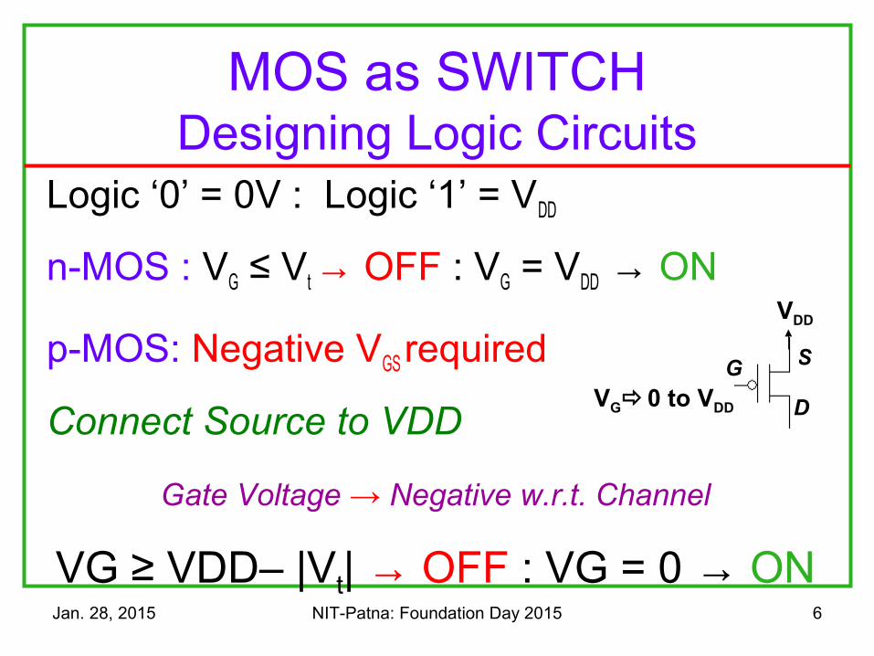
MOS as SWITCHDesigning Logic Circuits
Logic ‘0’ = 0V : Logic ‘1’ = VDD
n-MOS : VG ≤ Vt → OFF : VG = VDD → ON
p-MOS: Negative VGS required
Connect Source to VDD
Gate Voltage → Negative w.r.t. Channel
VG ≥ VDD– |Vt| → OFF : VG = 0 → ON
S
VDD
VG0 to VDD D
G
Jan. 28, 2015 NIT-Patna: Foundation Day 2015 7
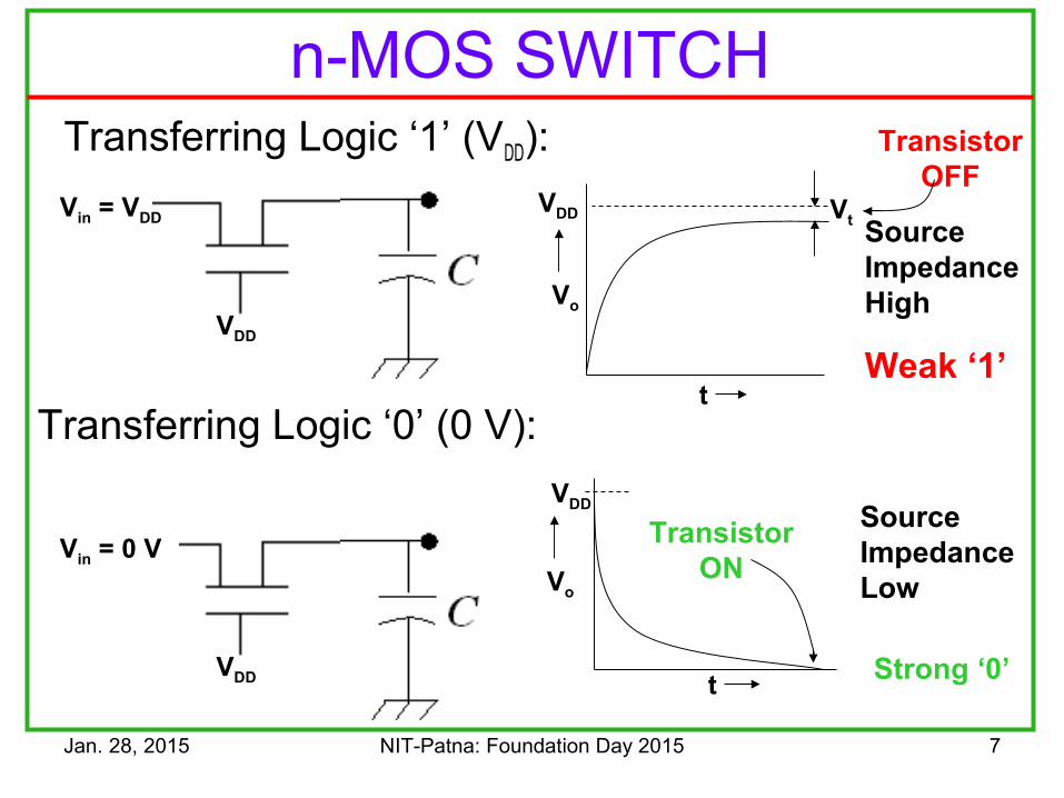
n-MOS SWITCHTransferring Logic ‘1’ (VDD):
VDD
Vin = VDD VtVDD
Vo
t
Transistor OFF
Source Impedance High
Weak ‘1’
Transistor ON
Source Impedance Low
Strong ‘0’VDD
Vin = 0 VVo
t
VDD
Transferring Logic ‘0’ (0 V):
Jan. 28, 2015 NIT-Patna: Foundation Day 2015 8
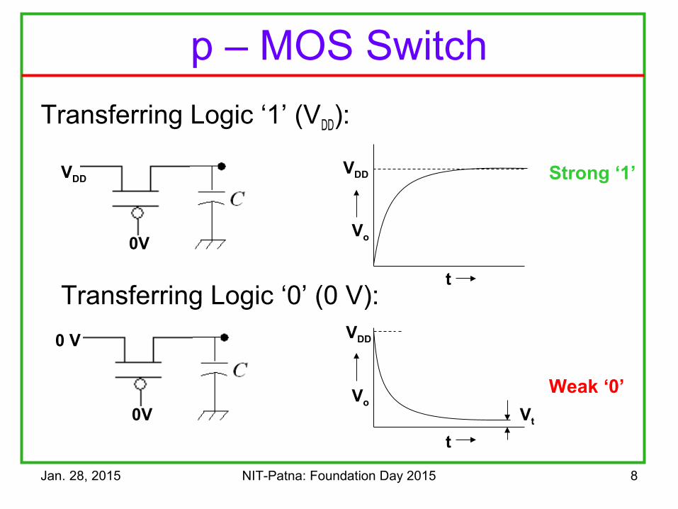
p – MOS Switch
Transferring Logic ‘1’ (VDD):
VDD
Vo
t
0V
VDD Strong ‘1’
Transferring Logic ‘0’ (0 V):
0V
0 V
t
Vo
VDD
Vt
Weak ‘0’
Jan. 28, 2015 NIT-Patna: Foundation Day 2015 9
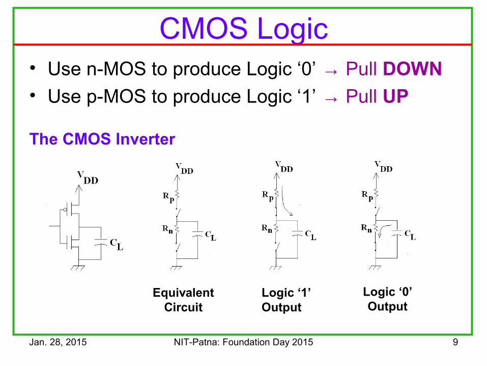
CMOS Logic• Use n-MOS to produce Logic ‘0’ → Pull DOWN• Use p-MOS to produce Logic ‘1’ → Pull UP
The CMOS Inverter
Equivalent Circuit
Logic ‘1’ Output
Logic ‘0’ Output
Jan. 28, 2015 NIT-Patna: Foundation Day 2015 10
Switching Theory
Revisited
MOS Circuit Design
Digital Logic
Jan. 28, 2015 NIT-Patna: Foundation Day 2015 11
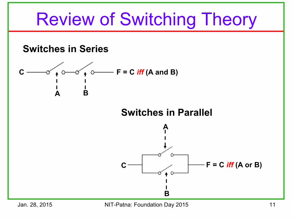
Review of Switching Theory
C
A B
F = C iff (A and B)
Switches in Series
A
B
C F = C iff (A or B)
Switches in Parallel
Jan. 28, 2015 NIT-Patna: Foundation Day 2015 12
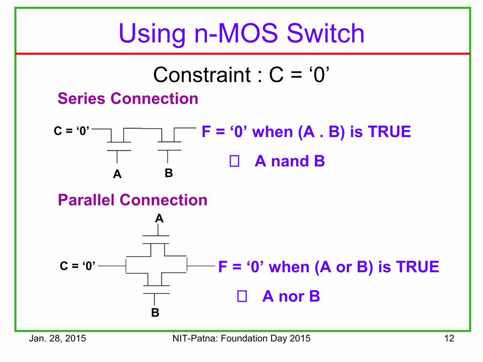
Using n-MOS Switch
Constraint : C = ‘0’
A B
Series Connection
C = ‘0’ F = ‘0’ when (A . B) is TRUE
⇒ A nand B
A
B
C = ‘0’ F = ‘0’ when (A or B) is TRUE
⇒ A nor B
Parallel Connection
Jan. 28, 2015 NIT-Patna: Foundation Day 2015 13
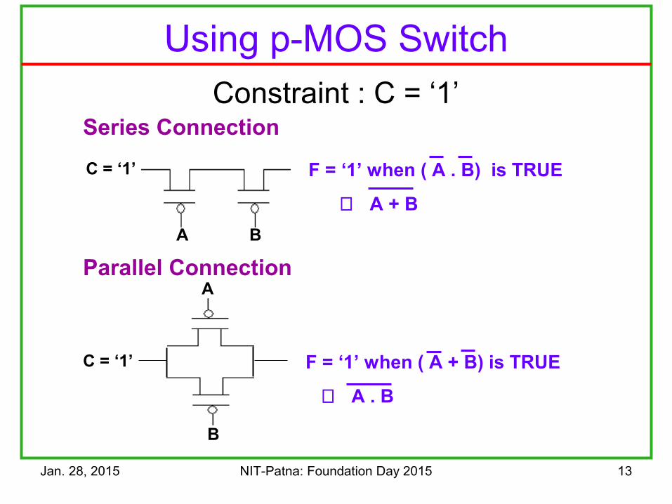
Using p-MOS SwitchConstraint : C = ‘1’
A B
C = ‘1’ F = ‘1’ when ( A . B) is TRUE
⇒ A + B
Series Connection
C = ‘1’
A
B
F = ‘1’ when ( A + B) is TRUE
⇒ A . B
Parallel Connection
Jan. 28, 2015 NIT-Patna: Foundation Day 2015 14
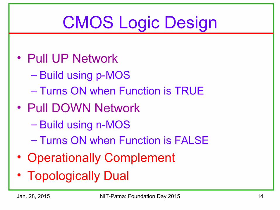
CMOS Logic Design
• Pull UP Network– Build using p-MOS– Turns ON when Function is TRUE
• Pull DOWN Network– Build using n-MOS– Turns ON when Function is FALSE
• Operationally Complement
• Topologically Dual
Jan. 28, 2015 NIT-Patna: Foundation Day 2015 15
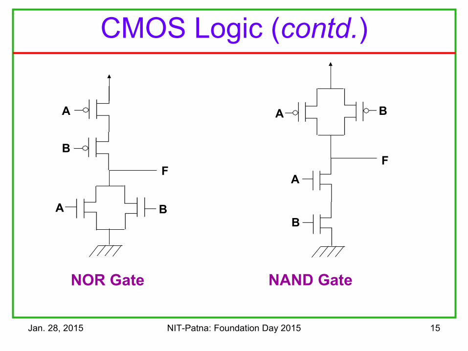
CMOS Logic (contd.)
A
A
B
BA
A
B
B
FF
NAND GateNOR Gate
Jan. 28, 2015 NIT-Patna: Foundation Day 2015 16
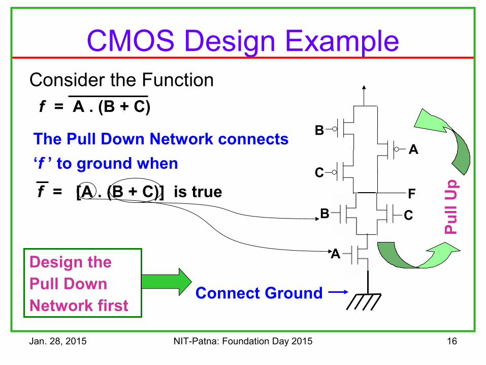
CMOS Design ExampleConsider the Function
f = A . (B + C)
Design the Pull Down Network first
A
B C
Pu
ll U
p
F
B
A
C
f = [A . (B + C)] is true
The Pull Down Network connects
‘f ’ to ground when
Connect Ground
Jan. 28, 2015 NIT-Patna: Foundation Day 2015 17
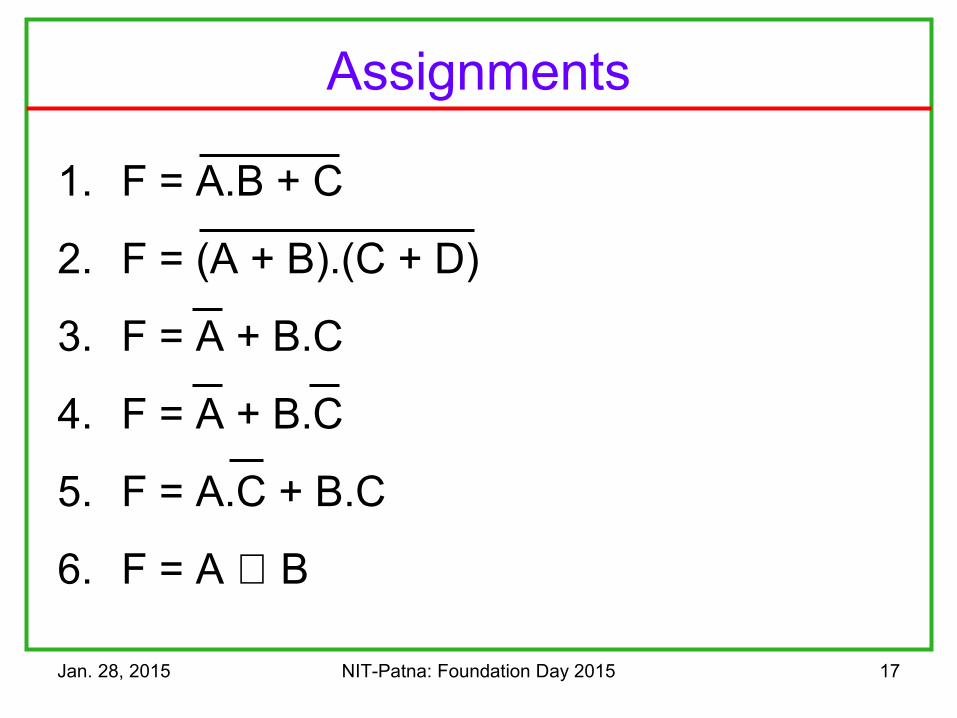
Assignments
1. F = A.B + C
2. F = (A + B).(C + D)
3. F = A + B.C
4. F = A + B.C
5. F = A.C + B.C
6. F = A ⊕ B
Steady State Input-Output Characteristics
Jan. 28, 2015 NIT-Patna: Foundation Day 2015 19
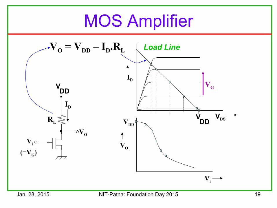
VDD
VO
Vi
(=VG)
MOS Amplifier
VDS
ID
VDD
VG
Vi
VO
Load Line
RL
ID
VO = VDD – ID.RL
VDD
Jan. 28, 2015 NIT-Patna: Foundation Day 2015 20
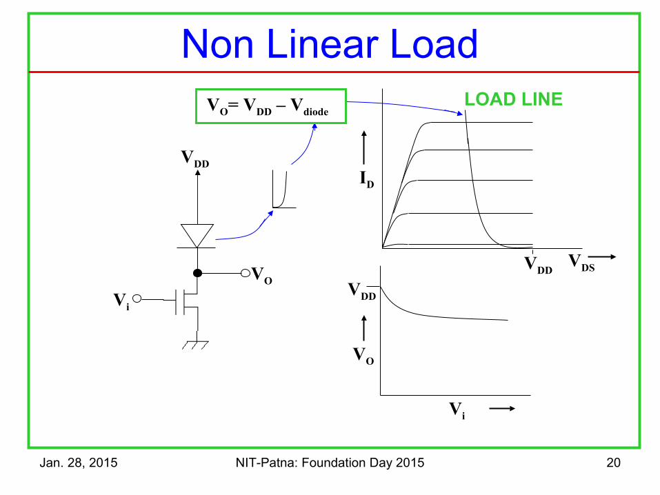
Non Linear Load
VDSVDD
ID
VDD
VO
Vi
LOAD LINEVO= VDD – Vdiode
VO
Vi
VDD
Jan. 28, 2015 NIT-Patna: Foundation Day 2015 21
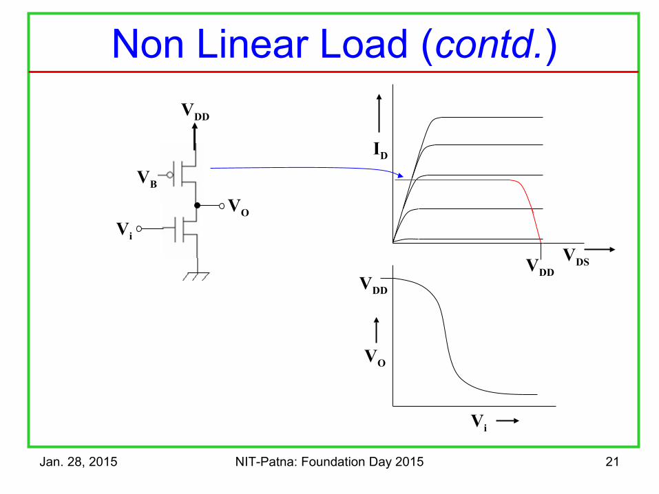
Non Linear Load (contd.)
Vi
VO
VB
VDD
VDD
VDS
ID
VDD
VO
Vi
Jan. 28, 2015 NIT-Patna: Foundation Day 2015 22
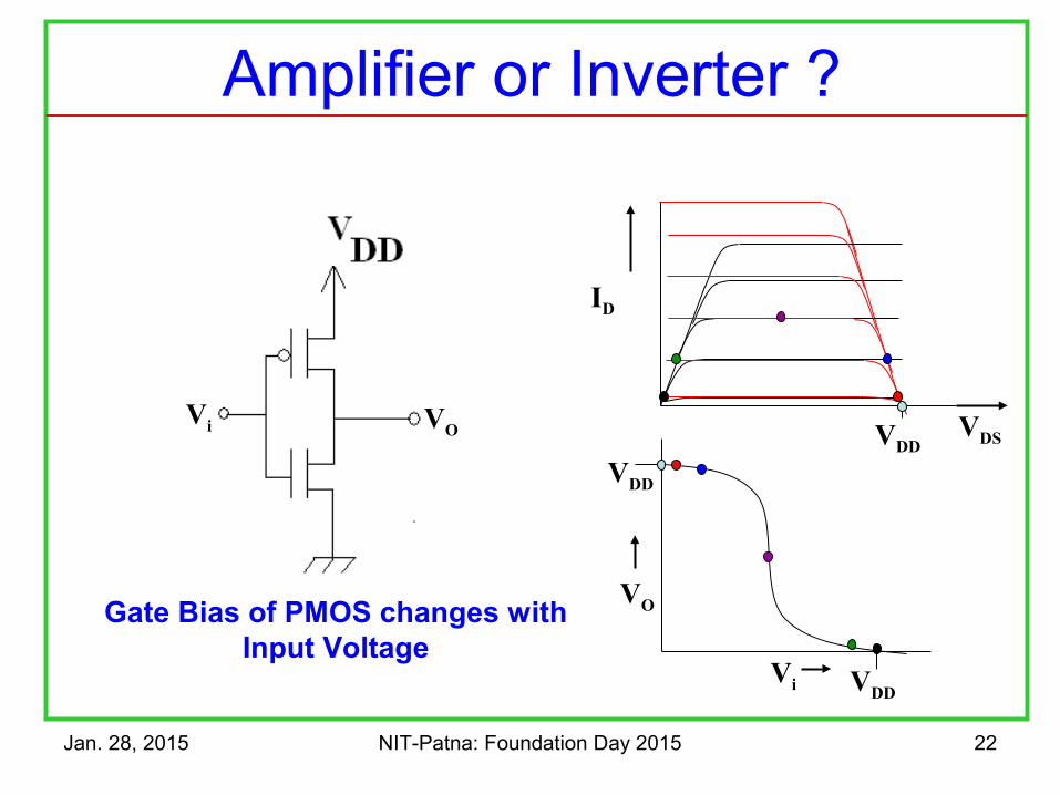
The CMOS InverterAmplifier or Inverter ?
Vi VO
VO
Vi
Gate Bias of PMOS changes with Input Voltage
VDD
VDDVDS
ID
VDD
Jan. 28, 2015 NIT-Patna: Foundation Day 2015 24
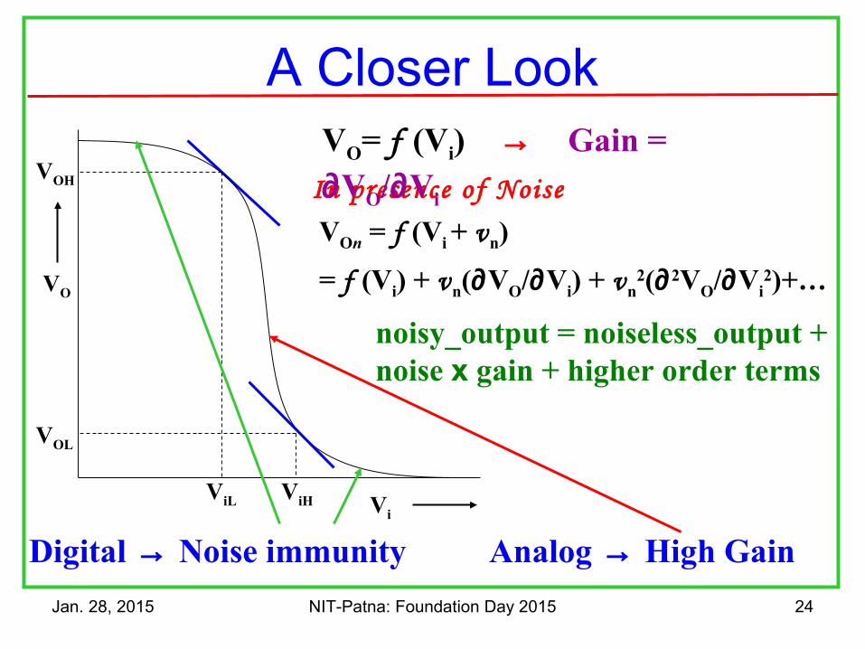
A Closer Look
In presence of Noise
VOn = f (Vi + vn)
= f (Vi) + vn(∂VO/∂Vi) + vn2(∂2VO/∂Vi
2)+…VO
Vi
noisy_output = noiseless_output +noise x gain + higher order terms
VO= f (Vi) → Gain = ∂VO/∂Vi
ViHViL
VOL
VOH
Digital → Noise immunity Analog → High Gain
Jan. 28, 2015 NIT-Patna: Foundation Day 2015 25
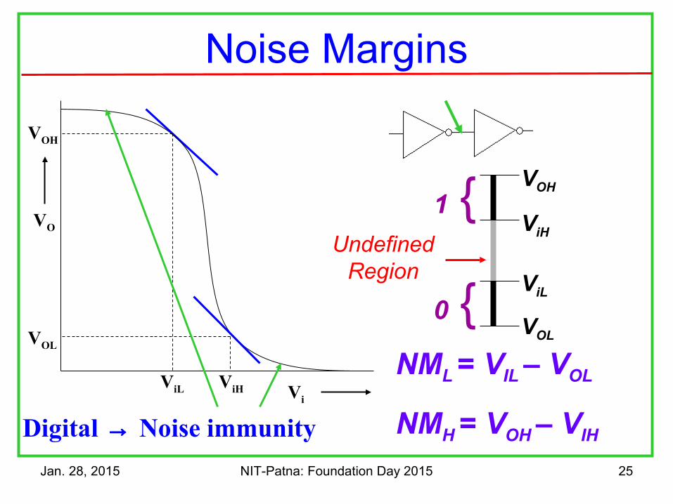
Noise Margins
VO
Vi
ViHViL
VOL
VOH
Digital → Noise immunity
NML = VIL – VOL
NMH = VOH – VIH
VOH
ViH
1 {
VOL
ViL
0 {Undefined
Region
Jan. 28, 2015 NIT-Patna: Foundation Day 2015 26
Vi VO
VO
Vi
VDD
VDDVDS
ID
VDD
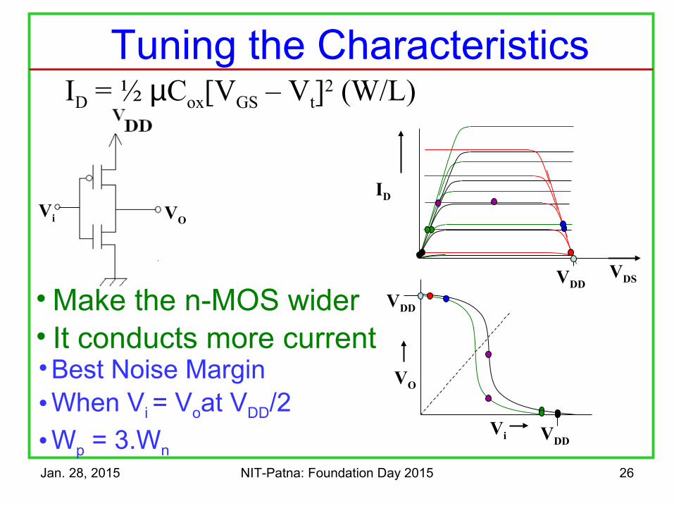
Tuning the Characteristics
• Make the n-MOS wider• It conducts more current
ID = ½ µCox[VGS – Vt]2 (W/L)
• Best Noise Margin • When Vi = Voat VDD/2
• Wp = 3.Wn
Jan. 28, 2015 NIT-Patna: Foundation Day 2015 27
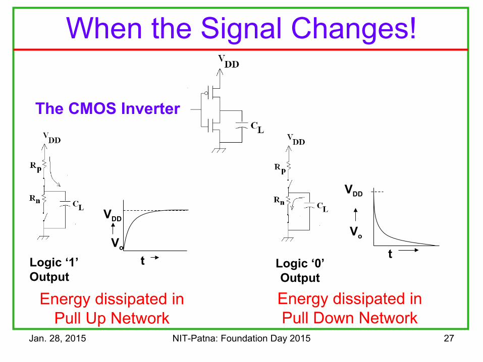
When the Signal Changes!
The CMOS Inverter
Logic ‘1’ Output
VDD
Vo
t Logic ‘0’ Output
Vo
t
VDD
Energy dissipated in Pull Up Network
Energy dissipated in Pull Down Network
Jan. 28, 2015 NIT-Patna: Foundation Day 2015 30
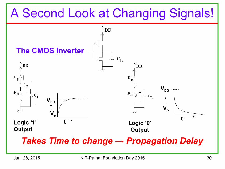
A Second Look at Changing Signals!
The CMOS Inverter
Logic ‘1’ Output
VDD
Vo
t Logic ‘0’ Output
Vo
t
VDD
Takes Time to change → Propagation Delay
Jan. 28, 2015 NIT-Patna: Foundation Day 2015 31
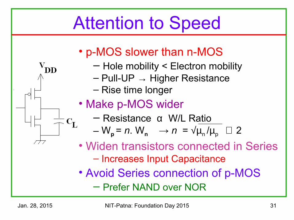
Attention to Speed
• p-MOS slower than n-MOS– Hole mobility < Electron mobility– Pull-UP → Higher Resistance– Rise time longer
• Make p-MOS wider– Resistance α W/L Ratio– Wp = n. Wn → n = √µn /µp ≅ 2
• Widen transistors connected in Series– Increases Input Capacitance
• Avoid Series connection of p-MOS– Prefer NAND over NOR
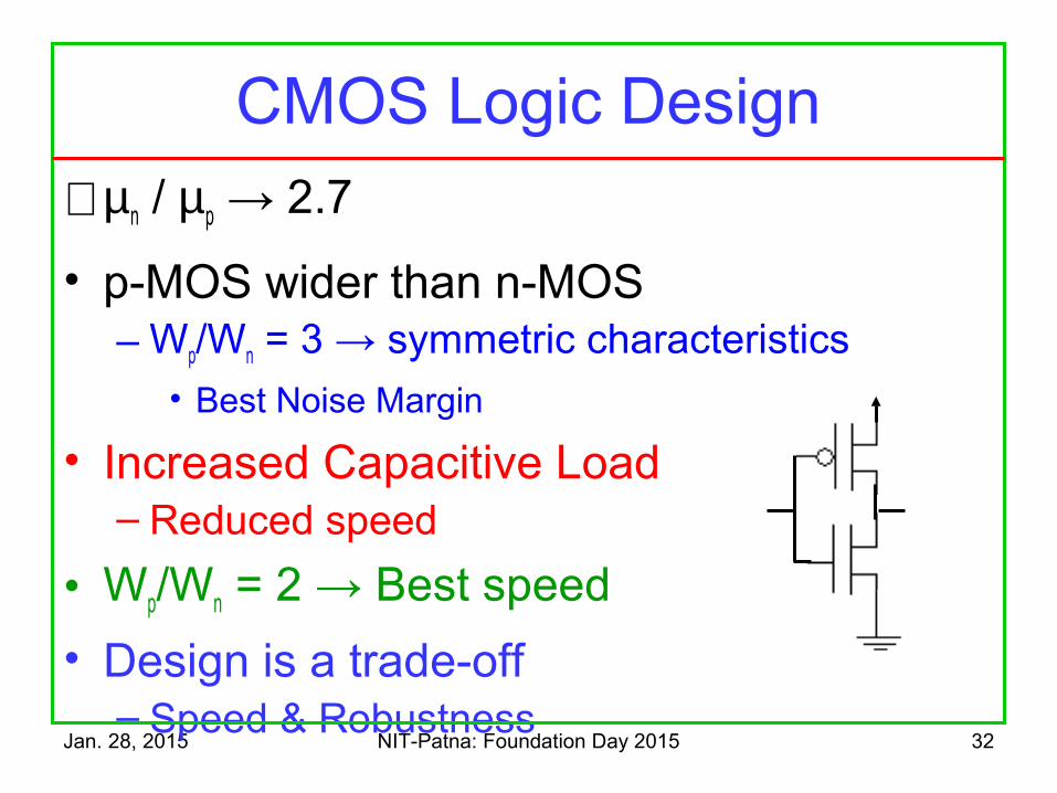
Jan. 28, 2015 NIT-Patna: Foundation Day 2015 32
∀ µn / µp → 2.7
• p-MOS wider than n-MOS– Wp/Wn = 3 → symmetric characteristics
• Best Noise Margin
• Increased Capacitive Load– Reduced speed
• Wp/Wn = 2 → Best speed
• Design is a trade-off – Speed & Robustness
CMOS Logic Design
Jan. 28, 2015 NIT-Patna: Foundation Day 2015 33
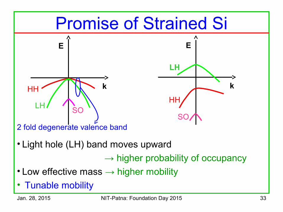
LHSO
E
k
HH
LH
SO2 fold degenerate valence band
E
kHH
• Light hole (LH) band moves upward
→ higher probability of occupancy• Low effective mass → higher mobility• Tunable mobility
Promise of Strained Si
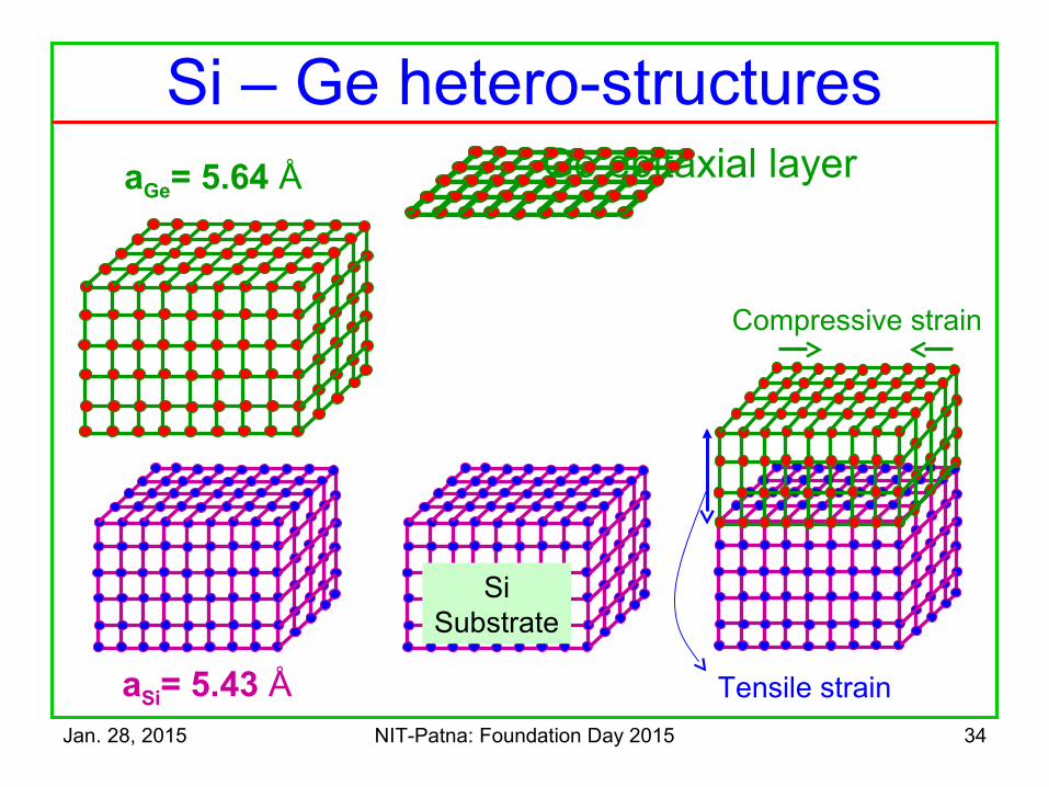
Jan. 28, 2015 NIT-Patna: Foundation Day 2015 34
a Si=
5.4
3 A aGe= 5.64 Å
Si Substrate
Ge epitaxial layer
Tensile strain
%2.40
0 =−=a
aaε
Si – Ge hetero-structures
aSi= 5.43 Å
Compressive strain
Jan. 28, 2015 NIT-Patna: Foundation Day 2015 35
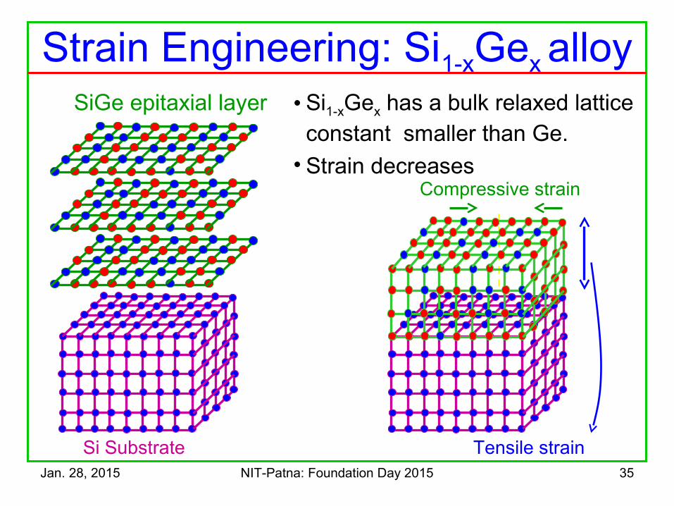
• Si1-xGex has a bulk relaxed lattice constant smaller than Ge.
• Strain decreases
Strain Engineering: Si1-xGex alloySiGe epitaxial layer
Si Substrate Tensile strain
Compressive strain
Jan. 28, 2015 NIT-Patna: Foundation Day 2015 36
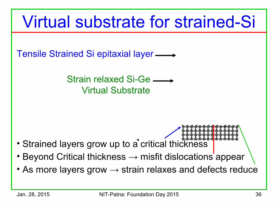
Virtual substrate for strained-Si
• Strained layers grow up to a critical thickness• Beyond Critical thickness → misfit dislocations appear• As more layers grow → strain relaxes and defects reduce
Strain relaxed Si-Ge Virtual Substrate
Tensile Strained Si epitaxial layer
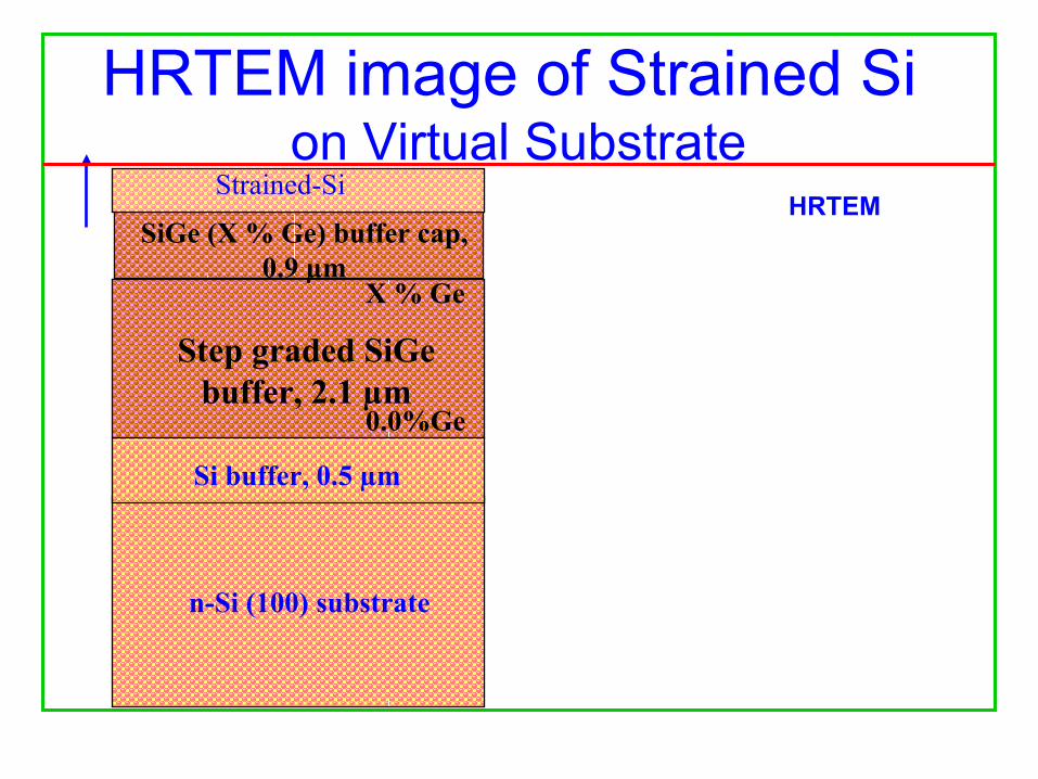
HRTEM image of Strained Si on Virtual Substrate
Strained-Si
SiGe (X % Ge) buffer cap, 0.9 µm
X % Ge
0.0%Ge
Step graded SiGe buffer, 2.1 µm
Si buffer, 0.5 µm
n-Si (100) substrate
HRTEM
Jan. 28, 2015 NIT-Patna: Foundation Day 2015 38
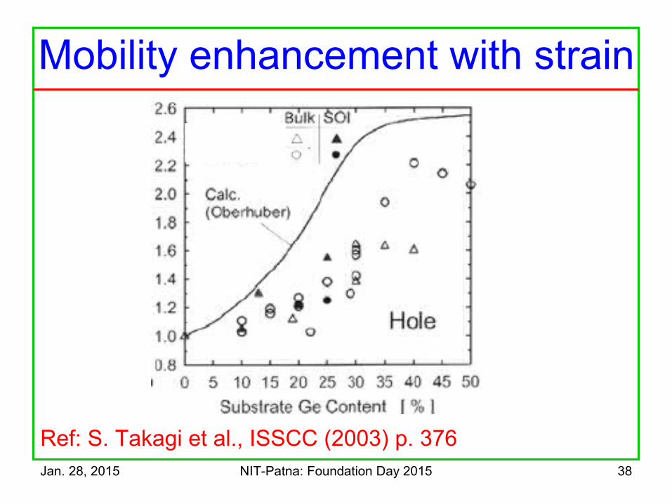
Ref: S. Takagi et al., ISSCC (2003) p. 376
Mobility enhancement with strain
Jan. 28, 2015 NIT-Patna: Foundation Day 2015 39
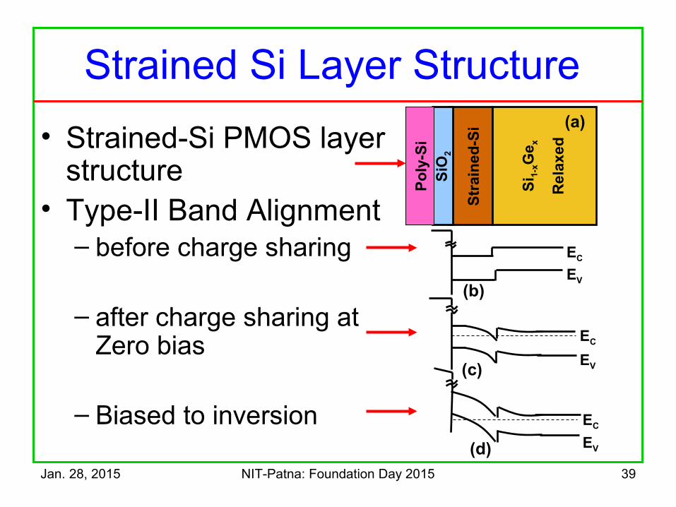
Strained Si Layer Structure
• Strained-Si PMOS layer structure
• Type-II Band Alignment– before charge sharing
– after charge sharing at Zero bias
– Biased to inversion
Si 1
-xG
e x
Rel
axed
Str
ain
ed-S
i
SiO
2
(a)
EC
EV
(b)
EC
EV(d)
EC
EV(c)
Po
ly-S
i
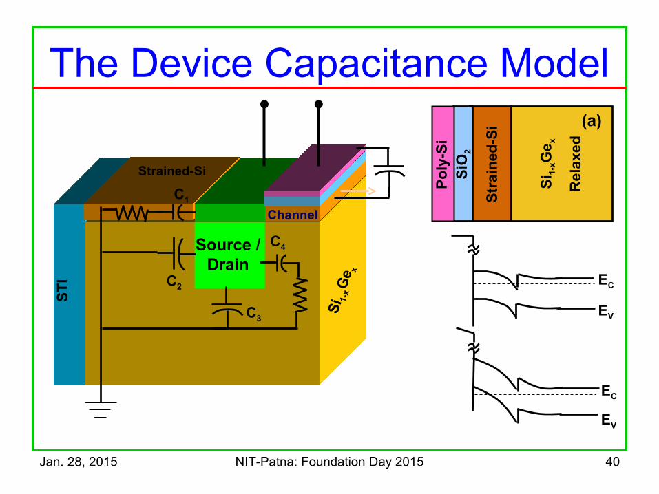
Jan. 28, 2015 NIT-Patna: Foundation Day 2015 40
The Device Capacitance Model
EC
EV
EC
EV
Si 1
-xG
e x
Rel
axed
SiO
2
(a)
Po
ly-S
i
Str
ain
ed-S
i
C1
C2
C3
ST
I
Channel
Strained-Si
Si 1-
xG
e x
C4Source / Drain
Jan. 28, 2015 NIT-Patna: Foundation Day 2015 41
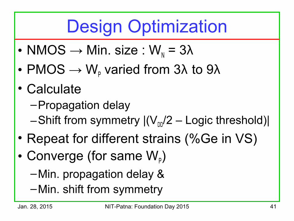
Design Optimization• NMOS → Min. size : WN = 3λ• PMOS → WP varied from 3λ to 9λ• Calculate
–Propagation delay–Shift from symmetry |(VDD/2 – Logic threshold)|
• Repeat for different strains (%Ge in VS)• Converge (for same WP)
–Min. propagation delay &–Min. shift from symmetry
Jan. 28, 2015 NIT-Patna: Foundation Day 2015 42
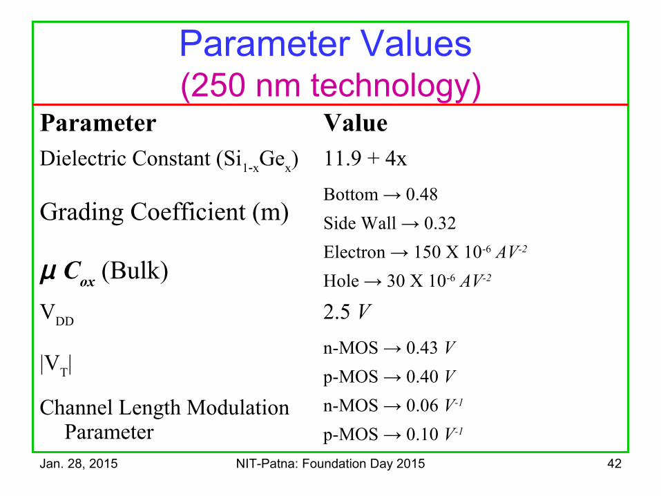
Parameter Values (250 nm technology)
Parameter ValueDielectric Constant (Si1 x‑ Gex) 11.9 + 4x
Grading Coefficient (m)Bottom → 0.48
Side Wall → 0.32
µ Cox (Bulk)Electron → 150 X 10-6 AV-2
Hole → 30 X 10-6 AV-2
VDD 2.5 V
|VT|n-MOS → 0.43 V
p-MOS → 0.40 V
Channel Length Modulation Parameter
n-MOS → 0.06 V-1
p-MOS → 0.10 V-1
Jan. 28, 2015 NIT-Patna: Foundation Day 2015 44
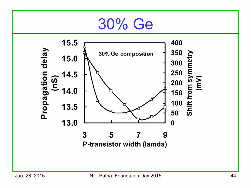
30% Ge
13.0
13.5
14.0
14.5
15.0
15.5
3 5 7 9P-transistor width (lamda)
Pro
pa
ga
tio
n d
ela
y
(nS
)
0
50
100
150
200
250
300
350
400
Sh
ift
fro
m s
ym
me
try
(m
V)
30% Ge composition
Jan. 28, 2015 NIT-Patna: Foundation Day 2015 45
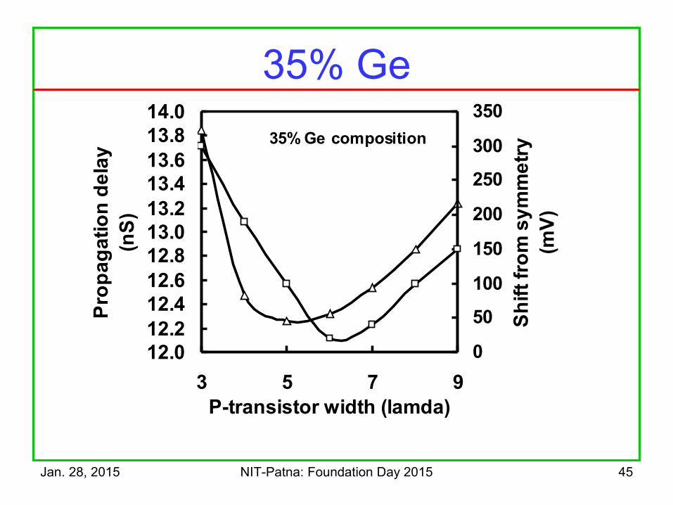
35% Ge
12.012.212.412.612.813.013.213.413.613.814.0
3 5 7 9P-transistor width (lamda)
Pro
pa
ga
tio
n d
ela
y
(nS
)
0
50
100
150
200
250
300
350
Sh
ift
fro
m s
ym
me
try
(m
V)
35% Ge composition
Jan. 28, 2015 NIT-Patna: Foundation Day 2015 46
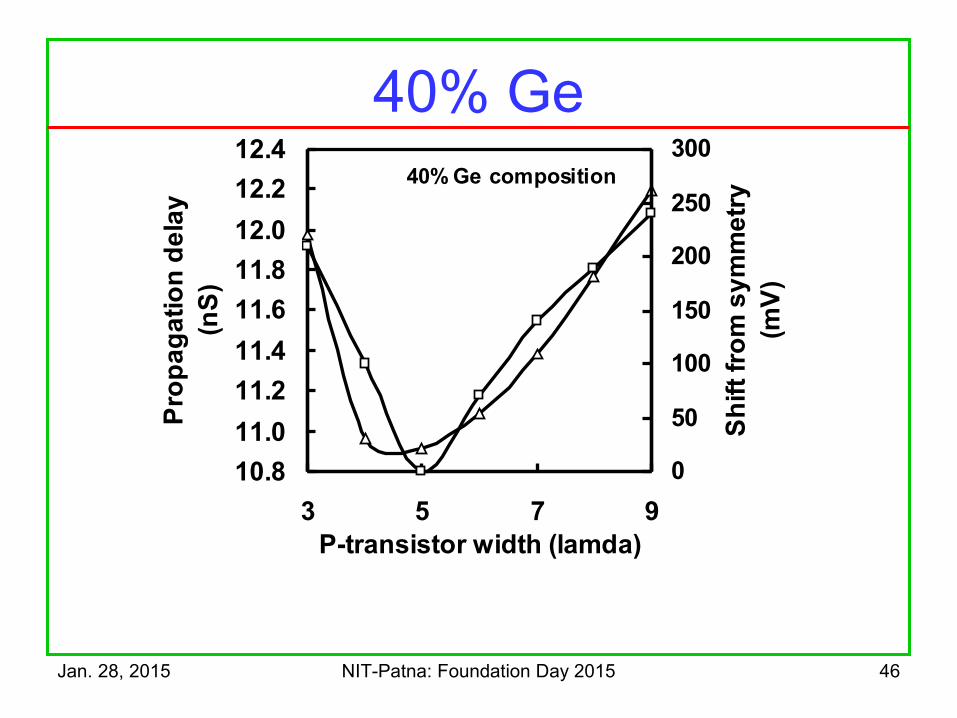
40% Ge
10.8
11.0
11.2
11.4
11.6
11.8
12.0
12.2
12.4
3 5 7 9P-transistor width (lamda)
Pro
pa
ga
tio
n d
ela
y
(nS
)
0
50
100
150
200
250
300
Sh
ift
fro
m s
ym
me
try
(m
V)
40% Ge composition
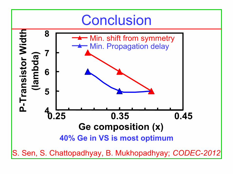
Min. shift from symmetryMin. Propagation delay
Summary
40% Ge in VS is most optimum
Conclusion
4
5
6
7
8
0.25 0.35 0.45Ge composition (x)
P-T
ran
sis
tor
Wid
th
(lam
bd
a)
S. Sen, S. Chattopadhyay, B. Mukhopadhyay; CODEC-2012
Jan. 28, 2015 NIT-Patna: Foundation Day 2015 48