transmission-line analogue of a drift transistor'€¦ · · 2014-01-14transmission-line...
TRANSCRIPT
R 361.,
Philips Res. Repts 14, 52-64, 1959,
TRANSMISSION-LINEANALOGUE OF A DRIFT TRANSISTOR'
by J. te WINKEL 621.314.7.012.8
SummaryA transmission line that is governed by the same differential equationsas a drift transistor is discussed. It provides a relatively simple way ofderiving the base transport parameters and the small-signal equivalentcircuit of the transistor, without solving the differential equationsexplicitly.
RésuméL'on discute ici d'une ligne de transmission de signaux électriques quiest soumise aux mêmes équations différentielles qu'un transistor àchamp interne. Cette ligne permet de trouver d'une façon assez simpleles paramètres et Ie circuit d'équivalence électrique du transistor sansqu'il soit nécessaire de résoudre explicitement les équations différen-tielles.
ZusammenfassungEs wird über eine Leitung gesprochen, die denselben Differentlalglei-chungen genügt wie ein Drifttransistor. Diese Leitung erlaubt auf ziem-lich einfache Weise die Bestimmung der Transistorparameter und desErsatzschaltbildes, wobei sich eine explizite Lösung der Differentlal-gleichungen erü brigt.
1. IntroductionIn a normal alloy transistor two differential equations describe the transport
of minority carriers in the base. They relate carrier currents and carrier coneen-trations and are of the same form as the equations relating currents and voltagesin a resistance-capacitance transmission line, a fact which has been usedoccasionally in the past 1).It will be shown that the transmission-line analogue concept can be extended
to a drift transistor. It then provides a relatively simple method of calculatingthe admittance parameters which determine the electrical properties of thetransistor as far as base transport is' concerned. The case which lends itselfmost easily to the analogue treatment is that of a constant drift field.
2. Condition for a constant drift fieldIt may be recalled that a constant drift field is obtained when the impurity
distribution in the base is an exponential one 2) 3). As the object is to improvetransistor performance, the impurity concentration has to be high near theemitter junction and low near the collector junction. A simple demonstrationcan. be given as follows.
TRANSMISSION-LINE ANALOGUE OF A DRIFT TRANSISTOR
. Consider the majority carrier flow in the base. Assuming a p-n-p transistor -.and a one-dimensional configuration, the electron current density jn is.the sumof a diffusion and a drift component, viz:
dnjn = q Dn - + q JLnnF,
. dx .
where n represents the electron concentration at a distance x from the emitter,F the drift field, q the absolute value of the electron charge, Dn and JLn the diffu-sion constant and the mobility for electrons, respectively. Under equilibriumconditions, that is, no external voltages applied to the transistor, this currentshould be zero. For a good transistor this will be very nearly so under normaloperati,ng conditions. Denoting the values of n at equilibrium by No and usingthe relation
»; kT-=-,JLn q
the condition jn = 0 leads toF dlnNo--=----.
kT/q dx
. Fx NeoIf F is independent of x, then -- - In -- orkT/q' No
No = Neo exp (_ Fx ).k/I'[q
Taking x = W, the base width, we have
FW Neo--=ln-,kT/q Nco,
where Neo and Nco represent the electron concentrations in the base at theemitter and collector junctions, respectively.The electron concentration No is practically equal to the donor (impurity)
concentration provided that it is large compared to the intrinsic carrier density.So eq. (1) prescribes an exponentially varying donor concentration as necessaryfor a constant drift field and eq. (2) links FW, the drift potential difference acrossthe base, with the donor concentration ratio, that is, Neo/Nco.
3. The analogue-
The transport through the base of minority carriers (holes), injected by theemitter, is governed by the following set of equations: '
'Ojp . qp 'Op-=---q-.'Ox T g( ,
. .'OpJp = -qDp- + q JLppF,
• ,'Ox
53
(1)
(2)
(3)
54 J. te WINKEL
In the first equation the current again is divided into a diffusion 'and a driftcomponent, p being the excess hole concentration. Itis assumed that the numberof holes injected is so small that it does not change the field by changing theelectron concentration. The second equation is the continuity equation, in whichthe left-hand side gives the difference between the number of holes, taken perunit of time, entering and leaving a certain volume element, and the right-handside. the number generated or lost by recombination and the number stored inthat element. The explanation of the symbols can be found in table I.
A set of transmission-line equations having the same form as the set (3) is
1 ov'i=---+Sv,
R ox.oi OV-=-Gv- C-··ox ot (4)
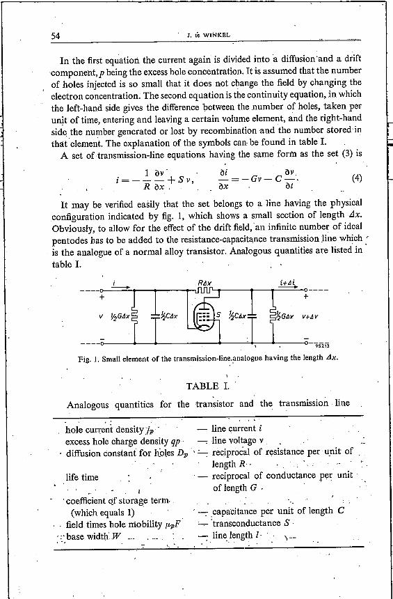
It may be verified easily that the set belongs to a line having the physicalconfiguration indicated by fig. 1, which shows a small section of length Llx.Obviously, to allow for the effect of the drift field,' an infinite number of idealpentodes has to be added to the resistance-capacitance transmission _line which 'is the analogue of a normal alloy transistor. Analogous quantities are listed' in .table I.
+
i+.ili-+
v ~G.ilx ~G.ilx V+.ilv
95213
Fig. 1. Small element of the transmission-line.analogue having the length Llx.
TABLE I.
Analogous quantities for the transistor and the transmission line
hole current density.Jp . - line current iexcess hole charge density qp --: line voltage v . .
. diffusion constant for holes Dp " ~ reciprocal of resistance per unit oflengthR· .
· - reciprocal of conductance p~~ unit :oflength G . .
life timeI
. coefficient of storage term. .(which equals 1)
field times hole mobility- fLpF
. z: base width', W. -. .
· -:- .capacitance per unit of length C· :....,...'transconductance S .--;-line.length Z· \ __
,TRANSMISSION-LINE ANALOGUE OF A DRIFT TRANSISTOR
.The.investigation of the properties of a drift transistor thus léads to the deriva-tion of the parameters of a transmissionline composed of an infinite number ofinfinitely small sections of the kind shown in fig. 1. .
1. Transmission-Iine parameters
The transmission line serving as transistor analogue differs from a normalline in t~e s~nse that the sections of which it may be imagined to be composedare non-symmetrical fourpoles. Equations (4) stilI can be solved in the classicalmanner; however, the alternative approach given in, the following lias theadvantage that it leads directly to the fourpole pa~ameters of the line, which arethe only quantities' of interest in the present case. This approach requires the useof iterative parameters as an intermediate step ..It may be recalled that the iterative admittance of a fourpole is defined as "an
admittance having such avalue that when if is connected between one pair ofterininals an adinittance of the same value is measured between the other pair,'
.. III general there is a separate value for each direction of transmission. Obviously,the two iterative admittances of a cascade of equal fourpoles are the same as theiterative admittances ofthe individual sections ofwhich it is composed. Another. set of iterative 'parameters (again one- for each direction of transmission). isobtained when one determines, in logarithmic units, the ratio of output and;~put voltages for the special case when the fourpole has its iterative adinittancesconnected between its terminals. Obviously again, the value for the cascade of anumber of equal sections is the value for the individual section multiplied bythat nûmber. ' . '
When a fourpole is given' in the conventional manner, for instanée by itsadinittance parameters, or in other words when the relation between voltagesand currepts at the two pairs of terminals is given as . , .
I ;:
the iterative parameters described above may be calculated. Conversely a givenset of iterative parameters may be converted into y parameters; see the Appendix.
Considering now the fourpole that represents a: small element of ,the trans-inission-line analogue as shown in fig. 1, one finds
" '
. :. , "', . "I)" 1 '.Yn = -f(G.+ jwC).tJx + R.tJx + S, '.
'. 1 ' i'Y12 =---,
R.tJx
Y21 . -(~~~. + ~)".. ' . i' i'. 1
-)'22. -f(G t jwC).tJ~ + .-..--.. ,". :,',' R61x.
55
(5)
(9)
56 J. te WINKEL
The iterative admittance of this single section transmitting from left to right is,according to eq. (AI) of the Appendix,
[G + jWC]!
ykl = -!-S+ t (GLlx + jwCLlx + S)2 + 4 R .
The same expression will apply for a' cascade. of a number of such sections.By letting zlx approach zero ykl will become the iterative admittance of the lineYkl. So
[G + jwC]!
Ykl = ts+ t S2 + 4 R . (6)
A useful simplification is obtained by putting
y = [tR2S2+ R(G +jwC)]!. (7)Then
YYkl = -!-S+-.
R(8)
Similarly when the direction of transmission is from right to left eq. (A3)gives
The logarithm of the voltage ratio in the case of iterative terminations willfollow from eq. (A2). For the elementary fourpole the result is
gkl = In (1+ S RLlx) -. [ S G+ jWC~i]-In I+tSRLlx+-!-R(G+jwC)(LlxF+-!-RLlx?(GLlx+jwCLlx+S)2+4 R S'
If now an infinite number of infinitely small elements is considered, gkl/Llxwill approach the voltage gain per unit of length. Expanding the logarithms anddividing by zlx then leads to
Gta. . . [ G+ jWC]iT = -!-SR - t R S2 + 4 R '.
where Gn. is the voltage gain of the line, iteratively terminated, and I its length.Introducing y again
Gkl = Ct 8R- y)l. (10)
In a similar manner for transmission in the other direction from eq. (A4),.1
'. Gk2= (-t SR-' y)l. - (11)
TRANSMIsSION-LINE ANALOGUE OF A DRIFT TRANSISTOR
. In order to obtain the admittance parameters of the transmission line, nowconsidered as a single fourpole, eqs (A13) from the Appendix have to be applied.Denoting these quantities by the symbols Yll, etc., one has
Y11= -iS + ~ coth "11,
"I e-iRSLY12=-~---'
R sinh "11"I e+iRSL
Y21=-~---,R sinh "11
"IY22= - -i S + - coth "11.
R
5. Transistor parameters
It is now an easy matter to replace the transmission-line quantities in eq. (12)by their transistor analogues. In particular
[f.Lp2F2 1 (1 . )]i"11= W -.-. - + - - + JW ,4Dp2 Dp T
and with eq. (2),f.LFW FW Neo
RSI=-- = --=ln-.o; kT/q N_co
Another useful simplification results when putting
FW---AkT/q - ,
and2DpW2 =Wo,
implying that A equals the drift potential across the base expressed in unitsk/I'[q and the Wo is the cut-off frequency of a transistor having the same basewidth as the one discussed here but where the drift :field is zero.
Hence W2 W"I1=tA2+-' +2j-,
L2 Wowhen using also L2 = DpT, and
RS1=A.
This leads to the following set of transistor parameters:
57
(12)
(13)
(14)
.(15)
(16)
58-,.~l -: .~:i. J.teWINKEL,~:·.:
(17)
," ,t
( .' ", .'. : ; • •• • .""' •• _. ....,.'... •• .... «Ó ~
where according to eq. (2) exp (-,tA) and exp C+tA) may ·be replaced by[Neo/Neo]t 'and [Neo/Neo]t, respectively. . . ·E:; .' .. " ,<As stated earlier, the analogues of the line voltage and the line current are
I' . . . "... .the excess hole charge density and the current de~sity in the transistor. Therefore.the set of parameters as given by eq. (17) will relate the hole concentrations inthe base near the emitter and collector junctions with the currèiitsentering thebase at those junctions ..Of course-strictly speaking, these parameters cannot becalled admittances any longer. Let now je and je represent current densities, whilePe and pc denote excess hole concentrations at the emitter. and collector junctionsrespectively, defining je positive when flowing outwards from the transistor.The relations between these quantities will .pe::' ; 1 -, ...
-: qYuPe'f.qY12Pe'l (18)je = - q YZl p« - q Y22 pc . S
rThis set of equations will suffice' to discuss' alternating currents as related tosinusoidally varying hole concentrations, as well as, by putting w = 0, direct
. currents' related-to :çsm.sta~t deviations of the hole concentrations :from .the:equilibrium valuen~~lng linear the 'set also describes the cQmbination'óf thesetwo cases. , , <: , "
6. Direct-current operation ". ." -Ó, ~' 1- . ' '., To relate direct currents 't~ direct voltages the excess hole concentrations in
, the base at the emitter and collector junctions, denoted by the symbols Pe andPc, should be expressed in the voltages applied to those junctions, Veb 'a~d Vc;:As' is well known, at the emitter :. ~ "
'.~'..'" E .:::::,n.' •. (. qVeb1kT"=1) .. ~, - _." ·e·· .r eO· e .. . " .
TRANSMISSION-LINÉ ANALOGUE OF A bRlFT TRANSISTOR. -
and at' the collector ..where PeO and Pco are the equilibrium values of'the hole concentratien at theemitter an'd collector junctions" respectively. .' "Inserting these two equations in (18), putting cu =~0 in the set of parameters
(17).and observing also that
PeONeo . Pco Nco = Ni2, .: /
(where Ni is the intrinsic carrier density), one obtains the direct-current densities,to be denoted by Je and Je, as
~e' q~~Ni2[~eo(!A+~tA~+ :~ycoth~~A2+ ~2n(é~e~/kT~1).~
W2*, ~tA2 + vf .
" - (éVcblkT - I)J. .! W2 t '~Neo Nco~ sinh ~tA2 + V ~
,7. Small-signal operation, equivalent circuit
'\ Alternating currents can simply be related to alternating voltages, providedthe latter are small compared to the direct voltages applied to the junctionssimultaneously. Differentiating eq. (19), which also represents the relationbetween instantaneous values, leads to
." . .Now dyeb _canbe identified with the alternating voltage across the junction an~.dPe with. the alternating part of 'the hole concentration. When these quantitiesa~e denoted by the symbols'Veb a~d pe (reserving from now on the symbol Pe' fotsmall variations only), one has . .'
.~.
'p - Po q'eQVeblkT v be - e kT' e • . (22)
In normal transistor operatien the collector-to-bäse' voltage is large -and:
(20)
(21)
"
60 J. te WINKEL
negative allowing to put exp (q Veb/kT) equal to zero. Assuming also thatW2/L2 ~ A2 it may be easily verified that eq. (21) reduces to
(23)
When now eqs (18) are taken as relating alternating currents to hole concentra-tion variations and when one puts P» = 0, which means that the alternatingvoltage at the collector is also zero, they reduce to
je = _q Y21Pe. (24)
Equations (22), (23) and (24) combined with Y11 and Y2,l from (17) and currentdensities J and j converted into currents I and i will allow to determine theemitterand collector currents resulting from an alternating voltage Veb appliedbetween emitter and base. From these will follow the transistor input and transferadmittances Yeb and Ym (which are admittances in 'the true sense now) andthe base transport factor f3: '
~W2 t» ~! ~ W2 w /'tA + tA2+-+ 2j- coth tA2 +- + 2j-(
ie qle L2 Wo L2 wo'~=-=- ,~Veb kT ~ W2~t ~ W2~i
tA + (l:A2 + L2) coth ~tA2 + £2)
~W2 w~!tA2+-+2j-L2 WoW2 os t'
sinh ~tA2+- + 2j -~? L2 wo)(26)
f3=ieie ____ tA --,.i sinh ~tA2+ _W_2+2j :::.l + cosh S,tA2+_W_2+ 2j :::.1'
~W2 w ~ ? L2 wo) ? L2 wo)
tA2 + - + 2j - . ,L2 Wo .
(27)
The other two transistor admittances, viz., the output admittance Yeb and thefeedback admittance Yj, could be determined in a similar way, putting P» = 0in (18), applying an alternating voltage Veb to the collector, and using relationssimilar to (22) and (23). However, the currents flowing in this case will be largelydetermined by another effect, which is the change of the collector depletion layerthickness with collector voltage (Early-effect). The corresponding change inthe effective base width will change the parameters (17).
TRANSMISSION·LINE ANALOGUE OF A DRIFT TRANSISTOR
If one now regards the fust equation (18) as representing both the directcurrent and the alternating current caused by the change in base width and ifone inserts a constant value for the hole concentration at the emitter (implyingthat the alternating voltage between emitter and base is zero) one obtains
Je + je = q PeYll(O) + q PedYll - qpcoY12(0) - qd(pcOY12),
where Yll (0) and Y!2(O) represent the values of Yll and Y22 for w = O.Separating direct and alternating currents in this equation and neglecting the
last term which can be shown to be small, one has
. dYll dWJe = qPe----dVCb.
dW dVCb
Here d Vcb can be identified with the alternating voltage at the collector Vcb.The feedback admittance Yf will be given by ie/Vcbwhen Veb= O.Thus with thehelp of (19) and (23) and conyerting current densities into currents,
leW 1 dYll dWYf =D . .~ W2~! ~ W2l dW dV .
P tA + (tA2 + L2 ~coth (tA2+ L2 ~ cb
In a similar manner, taking the second equation (18), the collector-ta-baseadmittan.ce is found to be
. kW 1 d~l dWYcb =D W2 t W2 ?t dW dV.. (29)
P tA + ~tA2+ .12 ~coth ~tA2+ L2 ~ cb
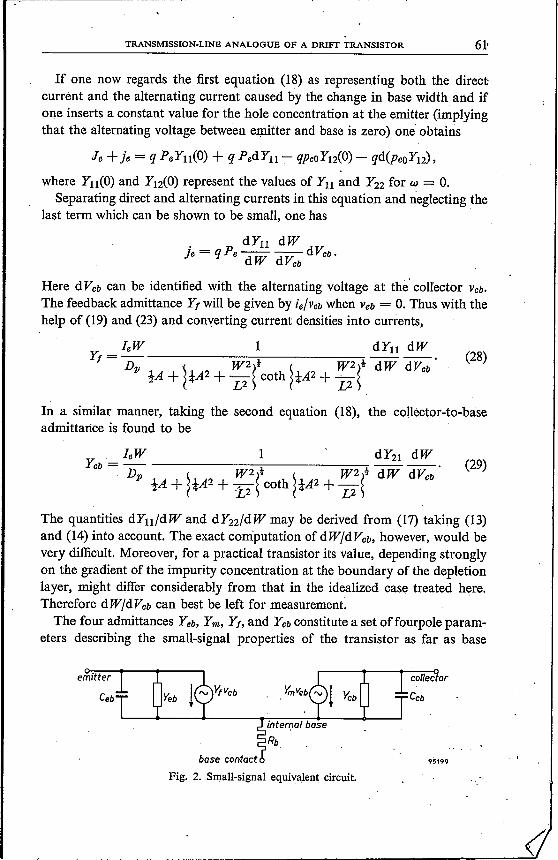
The quantities dYll/dW and dY22/dW may be derived from (17) taking (13)and (14) into account. The exact computation of dW/dVcb, however, would bevery difficult. Moreover, for a practical transistor its value, depending stronglyon the gradient of the impurity concentration at the boundary of the depletionlayer, might differ considerably from that in the idealized case treated here.Therefore dW/dVcb can best be left for measurement.The four admittances Yeb, Ym, Yf, and YCbconstitute a set of fourpole param-
eters describing the small-signal properties of the transistor as far as base
emitter
Ceb
Fig. 2. Small-signal equivalent circuit.
61'
(28)
62 J. Ie ytINKE[,.
transport is concerned. As such they also form the main part of the small-signalequivalent circuit of the complete transistor (fig. 2), the most important addi-tional elements, not discussed here, being the emitter and collector barriercapacitances and the base series resistance. On the other hand, under practicalconditions the expressions (25), (26), (28) and (29) can be simplified consider-ably 3). .
8. The case 'of a .varying drift field
If the drift field varies in a known way and if the rate of change is not toolarge, an approximate solution may be obtained by dividing the width of thebase into a number of parts and assuming the field to be constant within eachpart. The problem of finding the transistor parameters is thus reduced to thecalculation of the parameters of a fourpole which consists of a number of four-pbi~s i~ cascade; each representing the tra~smission-liné analogue of one of theparts into which the ?ase was divided. ..
Eindhoven, March 1958
- REFERENCES
1) A. van der Ziel, Proc. Inst. Radio Engrs 43, 1639-1646, 1955.2) K. Krö mer, Arch. elekt. Übertr. 8, 223-228, 1954.3) H. Krömer, Transistors I, R.C.A. Lab?ratories, Princeton, N.J., 1956, pp. 202-22Ó.
Appendix
the relations between admittance parameters and iterative parameters
Since the formulae that convert one kind of parameters into the other asgiven by most textbooks are restricted to symmetrical fourpoles, the espressionsfor the genelal case are derived below.
Let the fourpole equations be
il ;- YI) VI+ Y12 V2, i2 = Y21 VI + Y22 V2'
:The conneetlori of an admittance ykl between the pair of terminals 2 makesi2 = -Y~I V2, the admittance seen at the other pair will then be
il YI2Y2I- =Yll- ,VI Y22 -I- ykl
and the voltage ratioV2 Y2l-=-VI Y22 + ykl
In the case of iterative loading the input admittance should be again ykl> that is,il = ykl Vb leading to
ykl = !(Yll - Y22) + t ~(Yll + Y22)2 -AYI2Y21~?r. (Al)
TRANSMISSION-LINE ANALOGUE· OF A DRIFT TRANSISTOR
I
The logarithm of the voltageratio.then becomes', . :_ -
. V2:[ ,... -: 2Y21 ' . ']gleI = In - = In . . . . . .VI, Yll + Y22 + KJ!ll + Y22)2 _.:_4YI2Y21~!
When the transmission takes place in the reverse direction the load Ylè2-hasJo p,econnected between. the other, pair, of terminals. Interchanging in (AI) and (A2)the subscripts 1 and 2 gives '
'.'
yle2 = _:_t(Yll _:_;'22) + t ~(Yll + Y22)2 - 4YI2Y21~l;, (A3)... I" • -.'. ~ ( . 1
gk2 ~ In [Yll +y~ +)(y~l~~22)' ~ 4 Y12Y,:II]' (A4)
From the two possible vaiues of the square root on~ should t~ke the onewhich' makes the real 'part of the admittances positive.' , ".. . ~' ~:,
The reverse problem; finding the admittance parameters from the" iterativeparameters, can be solved as follows: ., "'."From (AI) and (A3) one deduces
I'
Yll - Y22 = yiel - yle2,
~(Yll + Y22)2 ~ 4 .r.i2Y21~t ='Yle~·-t- Yle;..""
From (A2) and (A4) one has'<
[Y21]l; : .:.: !' "
In - = t (gleI - gle2)Y12
[2 ~Y Y Ht ]I. 1 12 21ç l( + )n = '2 gleI gle2
Yu +Y22 + ~(Yll + Y22)2 - 4YI2Y2I~! '
or, after introducing hype~bolic functions and using the relation
cosh (In x) = t(x + x-I),
Y12 + Y2I ~ I2 ~ l* = cosh It (gleI - gle2)Ç ,
IY12Y21ç"
Yu + Y22 '} l2 } H = cosh l'! (gleI + gle2)Ç'
IYI2Y2IÇ ,
Squaring (A6) and (A8) and eliminating YI2Y2I yields
Yu + Y22 = -(Ylel + yk2) coth ~(t(gleI + gdt . (A9)"
Initially there are two signs possible in this equation; it may be verified,however, by inserting in (A9) the quantities specified by eqs (AI) to (A4), thatthe plus sign was introduced by .the squaring operation.
6~
(A2)
(A5)
(A6)
(A?)

64 J. te WINKEL
Eliminating Yu + Y22 from (A8) and (A9), we get
2 ~ 12 21H = _ yk1 + yk2 ..1Y Y ~ sinh ~t(gk1 + gk2)~
Combining (A7) and (AIO) gives
. cosh ~t(gk1 - gk2)~Y12 + Y21 = (Yk1 + yd . h~t( + )l .sm 1 gk1 gk2 ~
Squaring these last two equations and subtracting them gives
sinh ~t(gkl - gdtY12 - Y21 = - (Yk1 +yd . h ~t( + )(. (AI2)
sin 1 gk1 gk2 I
Here a similar remark applies as was made in connection with eq. (A9).Equations (A5), (A9), (All) and (AI2) finally will supply the admittance
parameters expressed in iterative parameters:
(AIO)
(All)
yu = t (Yk1 - yd - t (Yk1 + yk2) coth H· (gkl +gd~,e-i(gkl-gk2)
Y12 = t (Ykl + Yk2) . h)t ( '-+---:)l', sm 1 gk1 gk2 ~
e+ i(gkl -gk2)(A13)