tracking analogue to digital converter modelling using ... · tracking analogue to digital...
TRANSCRIPT
See discussions, stats, and author profiles for this publication at: https://www.researchgate.net/publication/283548251
Tracking Analogue to Digital Converter Modelling using VHDL-AMS
Conference Paper · June 2012
CITATIONS
0
READS
312
2 authors:
Some of the authors of this publication are also working on these related projects:
Analysis, design and modelling of analog and mixed-signal circuits and systems View project
“Study of the piezoelectric response of layered microgenerators on flexible substrates” View project
Marieta Kovacheva
Technical University of Sofia
13 PUBLICATIONS 10 CITATIONS
SEE PROFILE
Ivailo Milanov Pandiev
Technical University of Sofia
121 PUBLICATIONS 43 CITATIONS
SEE PROFILE
All content following this page was uploaded by Ivailo Milanov Pandiev on 07 November 2015.
The user has requested enhancement of the downloaded file.
Tracking Analogue to Digital Converter Modelling using VHDL-AMS
Marieta Kovacheva1 and Ivailo Pandiev2
Abstract – This paper describes a VHDL-AMS implementation of a behavioural model for tracking analogue to digital converter (ADC). For creating the model, simplification and build-up techniques known from modelling analogue integrated circuits have been adapted. This generalized model is independent from actual technical realizations and is based upon compromises regarding the representation of exact circuit structure in the model. The proposed tracking ADC model accurately predicts the circuit behaviour for dc and transient responses. Its beha-viour is created consequently using tracking ADC basic struc-ture. The modelling of the ADC behaviour is implemented and confirms to the format of the simulation program System Vision 5.5 (from Mentor Graphics). The simulation results show accu-rate agreement with the theoretical predictions.
Keywords – Mixed-signal circuits, Analogue to digital conver-ters, Counting method, Tracking ADCs, VHDL-AMS, Mixed-signal simulation.
I. INTRODUCTION
An analogue to digital converter (ADC) is a device that converts a continuous quantity to a discrete time digital representation. Typically, an ADC is an electronic device that converts an input analogue voltage or current to a digital number proportional to the magnitude of the voltage or the current. The digital output may use different coding schemes. Basically there are three different conversion methods: (1) parallel method (convert a word at a time), (2) weighting method (convert a digit at a time) and (3) counting method (convert a level at a time). In Table 1, is shown a comparison between three basic methods of conversion [1-4]. The benefits of the tracking converters are that (1) their output is continuously available and (2) their accuracy is very high. The main drawback of tracking ADC is their slow step response, however, this is compensated with their possibility of large resolution (12-,14-,16- bits).
After analyze of the existing model libraries in OrCAD PSpice A/D [5], SystemVision (from Mentor Graphics) [6] and Matlab Simulink [7] some conclusions are made. In System Vision libraries an ADC behavioural model can be found, but it works by using successive-approximation method and its resolution is fixed to 10 bits, others types of converters are not included. In OrCAD PSpice A/D libraries exists simulation model of ADC – called ADC8, ADC10 or
ADC12. Its resolution can be set as 8 -, 10 - or 12-bit. In the PSpice based model the voltage at in mode and ref mode with respect to ground mode is sampled starting at the rising edge of the convert signal and ending when the status goes high. These models with a suitable choice of parameters and elements can be used of a mixed-signal circuit simulations, but not confirm to the architectures of a broad class of the monolithic ADCs. Transformation from OrCAD PSpice A/D to System Vision libraries can be done, but it’s quite complicated, requires a lot of resources and additional processing. In Matlab Simulink exists one ADC model, called idealized ADC quantizer with the following changeable parameters: (1) number of converted bits, (2) minimum and maximum output voltage and (3) output data type. This model is generalized structure and cannot be used for several specific applications. Also an investigation in the published articles was made and the conclusions are following – found one article describing a VHDL implementation of a behavioural model for pipeline ADCs by using VHDL description to facilitate the synthesis of the digital part [8], another one for simulation tools in designing sigma delta ADC and its efficiency by using both Simulink and VHDL-AMS [9] and the last one presents behavioural VHDL-AMS model for monolithic Half-Flash (Two Step) 10-bit ADC [10]. The goal of this paper is to develop a behavioural VHDL-AMS model that accurately simulates the basic characteristics of tracking ADCs.
TABLE 1 COMPARISON OF CONVERSION METHODS
ADC types Number
of clocks
Number of reference voltages
Characteristics
Parallel (Flash) method
1
12 −n
very fast; needs many parts ( 12 −n compa-rators); lower resolu-tion, expensive; large power consumption
Successive-approximation method
n
n
capable of high speed; medium accuracy; good tradeoff between speed and cost; speed limited ~ 5Msps; require S/H circuit
Counting method
max n2
1
input signal is avera-ged; greater noise immunity; high accuracy; slow; require S/H circuit
II. PRINCIPLE OF TRACKING CONVERTERS OPERATION
The counting method requires the least circuit complexity, but the conversion time is considerably longer than with the
1Marieta Kovacheva is with the Faculty of Electronics atTechnical University of Sofia, 8 Kl. Ohridski Blvd, Sofia 1000,Bulgaria, E-mail: [email protected].
2Ivailo Pandiev is with the Faculty of Electronics at TechnicalUniversity of Sofia, 8 Kl. Ohridski Blvd, Sofia 1000, Bulgaria.E-mail: [email protected].
I C E S T 2012 28-30 JUNE, 2012, VELIKO TARNOVO, BULGARIA
224
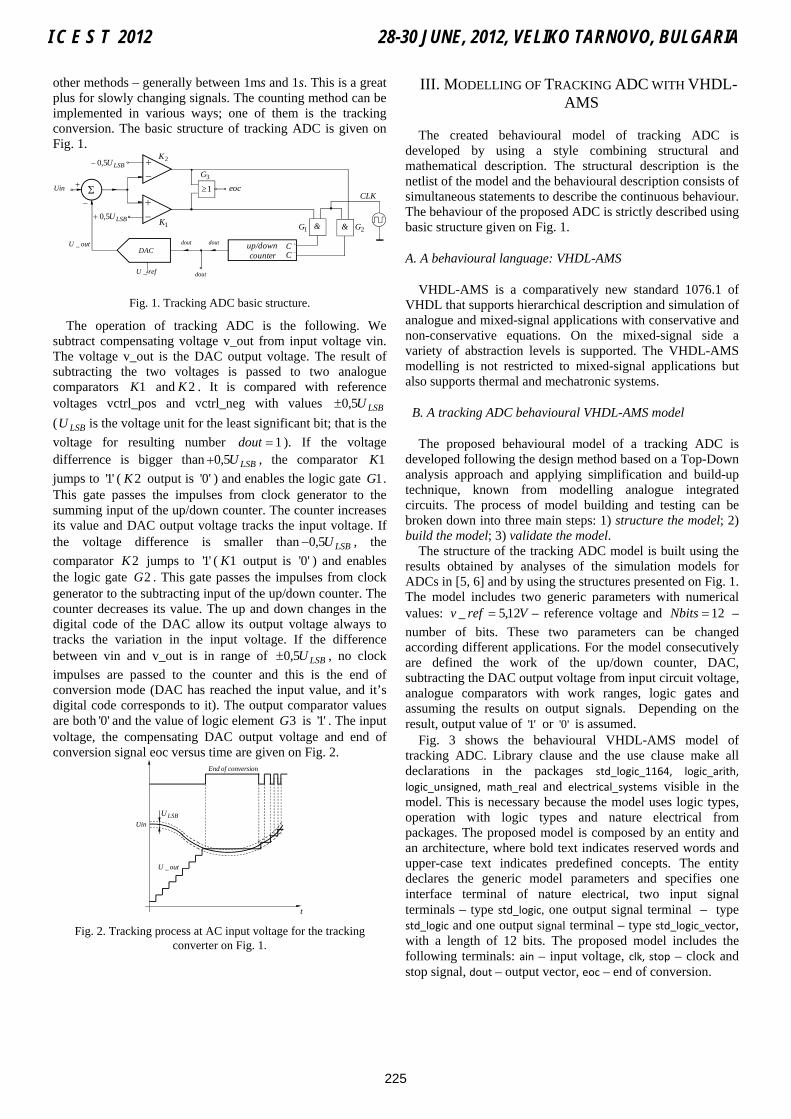
other methods – generally between 1ms and 1s. This is a great plus for slowly changing signals. The counting method can be implemented in various ways; one of them is the tracking conversion. The basic structure of tracking ADC is given on Fig. 1.
2K
outU _
dout
up/down counter
+C−C
1K
LSBU5,0−
LSBU5,0+
Σ+ 1≥ eoc
& &1G 2G
3G
−
DAC
CLK
doutdout
Uin
refU _
Fig. 1. Tracking ADC basic structure.
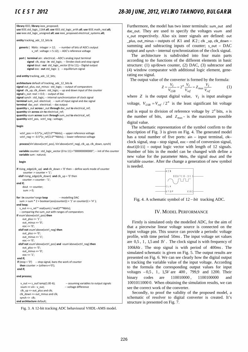
The operation of tracking ADC is the following. We subtract compensating voltage v_out from input voltage vin. The voltage v_out is the DAC output voltage. The result of subtracting the two voltages is passed to two analogue comparators 1K and 2K . It is compared with reference voltages vctrl_pos and vctrl_neg with values LSBU5,0± ( LSBU is the voltage unit for the least significant bit; that is the voltage for resulting number 1=dout ). If the voltage differrence is bigger than LSBU5,0+ , the comparator 1K jumps to '1' ( 2K output is '0' ) and enables the logic gate 1G . This gate passes the impulses from clock generator to the summing input of the up/down counter. The counter increases its value and DAC output voltage tracks the input voltage. If the voltage difference is smaller than LSBU5,0− , the comparator 2K jumps to '1' ( 1K output is '0' ) and enables the logic gate 2G . This gate passes the impulses from clock generator to the subtracting input of the up/down counter. The counter decreases its value. The up and down changes in the digital code of the DAC allow its output voltage always to tracks the variation in the input voltage. If the difference between vin and v_out is in range of LSBU5,0± , no clock impulses are passed to the counter and this is the end of conversion mode (DAC has reached the input value, and it’s digital code corresponds to it). The output comparator values are both '0' and the value of logic element 3G is '1' . The input voltage, the compensating DAC output voltage and end of conversion signal eoc versus time are given on Fig. 2.
t
outU _
LSBU
End of conversion
Uin
Fig. 2. Tracking process at AC input voltage for the tracking
converter on Fig. 1.
III. MODELLING OF TRACKING ADC WITH VHDL-AMS
The created behavioural model of tracking ADC is developed by using a style combining structural and mathematical description. The structural description is the netlist of the model and the behavioural description consists of simultaneous statements to describe the continuous behaviour. The behaviour of the proposed ADC is strictly described using basic structure given on Fig. 1.
A. A behavioural language: VHDL-AMS
VHDL-AMS is a comparatively new standard 1076.1 of VHDL that supports hierarchical description and simulation of analogue and mixed-signal applications with conservative and non-conservative equations. On the mixed-signal side a variety of abstraction levels is supported. The VHDL-AMS modelling is not restricted to mixed-signal applications but also supports thermal and mechatronic systems.
B. A tracking ADC behavioural VHDL-AMS model
The proposed behavioural model of a tracking ADC is developed following the design method based on a Top-Down analysis approach and applying simplification and build-up technique, known from modelling analogue integrated circuits. The process of model building and testing can be broken down into three main steps: 1) structure the model; 2) build the model; 3) validate the model.
The structure of the tracking ADC model is built using the results obtained by analyses of the simulation models for ADCs in [5, 6] and by using the structures presented on Fig. 1. The model includes two generic parameters with numerical values: Vrefv 12,5_ = – reference voltage and 12=Nbits – number of bits. These two parameters can be changed according different applications. For the model consecutively are defined the work of the up/down counter, DAC, subtracting the DAC output voltage from input circuit voltage, analogue comparators with work ranges, logic gates and assuming the results on output signals. Depending on the result, output value of '1' or '0' is assumed.
Fig. 3 shows the behavioural VHDL-AMS model of tracking ADC. Library clause and the use clause make all declarations in the packages std_logic_1164, logic_arith, logic_unsigned, math_real and electrical_systems visible in the model. This is necessary because the model uses logic types, operation with logic types and nature electrical from packages. The proposed model is composed by an entity and an architecture, where bold text indicates reserved words and upper-case text indicates predefined concepts. The entity declares the generic model parameters and specifies one interface terminal of nature electrical, two input signal terminals – type std_logic, one output signal terminal – type std_logic and one output signal terminal – type std_logic_vector, with a length of 12 bits. The proposed model includes the following terminals: ain – input voltage, clk, stop – clock and stop signal, dout – output vector, eoc – end of conversion.
I C E S T 2012 28-30 JUNE, 2012, VELIKO TARNOVO, BULGARIA
225
library IEEE; library ieee_proposed; use IEEE.std_logic_1164.all; use IEEE.std_logic_arith.all; use IEEE.math_real.all; use ieee.std_logic_unsigned.all; use ieee_proposed.electrical_systems.all; entity tracking_adc_12_bits is generic ( Nbits : integer := 12; ‐‐ number of bits of ADC's output v_ref : voltage := 5.12); ‐‐ ADC's reference voltage port ( terminal ain : electrical; ‐‐ADC's analog input terminal signal clk, stop : in std_logic; ‐‐ Strobe clock and stop signal signal dout : out std_logic_vector (0 to 11);‐‐ Digital output signal eoc : out std_logic ); ‐‐ equilibrium signal end entity tracking_adc_12_bits; architecture default of tracking_adc_12_bits is signal out_plus, out_minus: std_logic; ‐‐ output of comparators signal clk_up, clk_down: std_logic; ‐‐ up and down input of the counter signal s_out: real := 0.0; ‐‐ output of dac signal synch : std_logic; ‐‐ internal synchronization of clock signal terminal sum_out: electrical; ‐‐ sum of input signal and dac signal terminal dac_out : electrical; ‐‐ dac output quantity v_out across i_out through dac_out to electrical_ref; quantity vin across ain to electrical_ref; quantity vsum across isum through sum_out to electrical_ref; quantity vctrl_pos, vctrl_neg : voltage; begin vctrl_pos == 0.5*(v_ref/2.0**Nbits); ‐‐ upper reference voltage vctrl_neg == ‐0.5*(v_ref/2.0**Nbits); ‐‐ lower reference voltage process(Vin'above(vctrl_pos), Vin'above(vctrl_neg), clk_up, clk_down, synch) variable counter : std_logic_vector (0 to 11):="000000000000"; ‐‐ init of the counter variable sum : natural; begin if rising_edge(clk_up) and clk_down = '0' then ‐‐ define work mode of counter counter := counter + '1'; elsif rising_edge(clk_down) and clk_up = '0' then counter := counter ‐ '1'; end if; dout <= counter; sum := 0; for i in counter'range loop ‐‐ modelling DAC sum := sum * 2 + boolean'pos(counter(i) = '1' or counter(i) = 'H' ); end loop; s_out <= v_ref * real(sum) / real(2**Nbits); ‐‐ comparing the sum_out with ranges of comparators if vsum'above(vctrl_pos) then out_plus <= '1' ; out_minus <= '0'; eoc <= '0'; elsif not vsum'above(vctrl_neg) then out_plus <= '0'; out_minus <= '1'; eoc <= '0'; elsif not vsum'above(vctrl_pos) and vsum'above(vctrl_neg) then out_plus <= '0'; out_minus <= '0'; eoc <= '1'; end if; if (stop = '0') ‐‐ stop signal, bans the work of counter then counter := (others=>'0'); end if; end process; v_out == s_out'ramp(1.0E‐6); ‐‐ assuming variables to output signals vsum == vin ‐ v_out; ‐‐ voltage difference clk_up <= out_plus and clk; clk_down <= out_minus and clk; synch <= clk; end architecture default;
Fig. 3. A 12-bit tracking ADC behavioural VHDL-AMS model.
Furthermore, the model has two inner terminals: sum_out and dac_out. They are used to specify the voltages vsum and v_out respectively. Also six inner signals are defined: out _plus, out_minus – outputs of 1K and 2K ; clk _up, clk_down – summing and subtracting inputs of counter; s_out – DAC output and synch – internal synchronization of the clock signal. The architecture is subdivided into four main parts according to the functions of the different elements in basic structure: (1) up/down counter, (2) DAC, (3) subtractor and (4) window comparator with additional logic element, gene-rating eoc signal.
The output value of the converter is formed by the formula:
ref
I
ref
In
LSB
IVVZ
VV
VVZ max2 === (1)
where Z is the output digital value, IV is input analogue
voltage, nrefLSB VV 2/= is the least significant bit voltage
and is equal to division of reference voltage by n2 bits, n is the number of bits, and maxZ - is the maximum possible digital value. The schematic representation of the symbol confirm to the description of Fig. 3 is given on Fig. 4. The generated model has a total number of five ports: ain – input terminal, clk– clock signal, stop - stop signal, eoc – end of conversion signal, dout1[0:11] – output logic vector with length of 12 signals. Number of bits in the model can be changed with define a new value for the parameter Nbits, the signal dout and the variable counter. After the change a generation of new symbol is needed.
Fig. 4. A schematic symbol of bit−12 tracking ADC.
IV. MODEL PERFORMANCE
Firstly is simulated only the modelled ADC, for the aim of that a piecewise linear voltage source is connected on the input voltage pin. This source can provide a periodic voltage profile, with time period ms50 . The input voltage set values are 5,0 , 1 , 5,1 and V1 . The clock signal is with frequency of
kHz100 . The stop signal is with period of ms400 . The simulated schematic is given on Fig. 5. The output results are presented on Fig. 6. We can see clearly how the digital output is tracking the variable value of the input voltage. According to the formula the corresponding output values for input voltages – 5,0 , 1 , V5,1 are 400 , 9,799 and 1200. Their binary codes are 110010000 , 1100100000 and
.01001011000 When obtaining the simulation results, we can see the correct work of the converter. Secondly, to proof the validity of the proposed model, a schematic of resolver to digital converter is created. It’s structure is presented on Fig. 7.
I C E S T 2012 28-30 JUNE, 2012, VELIKO TARNOVO, BULGARIA
226
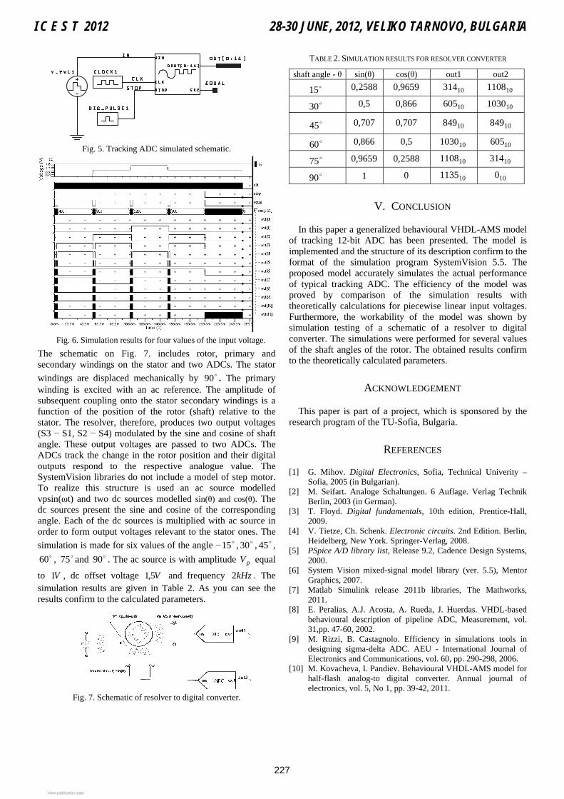
Fig. 5. Tracking ADC simulated schematic.
Fig. 6. Simulation results for four values of the input voltage.
The schematic on Fig. 7. includes rotor, primary and secondary windings on the stator and two ADCs. The stator windings are displaced mechanically by o90 . The primary winding is excited with an ac reference. The amplitude of subsequent coupling onto the stator secondary windings is a function of the position of the rotor (shaft) relative to the stator. The resolver, therefore, produces two output voltages (S3 − S1, S2 − S4) modulated by the sine and cosine of shaft angle. These output voltages are passed to two ADCs. The ADCs track the change in the rotor position and their digital outputs respond to the respective analogue value. The SystemVision libraries do not include a model of step motor. To realize this structure is used an ac source modelled vpsin(ωt) and two dc sources modelled sin(θ) and cos(θ). The dc sources present the sine and cosine of the corresponding angle. Each of the dc sources is multiplied with ac source in order to form output voltages relevant to the stator ones. The simulation is made for six values of the angle − o15 , o30 , o45 ,
o60 , o75 and o90 . The ac source is with amplitude pV equal
to V1 , dc offset voltage V5,1 and frequency kHz2 . The simulation results are given in Table 2. As you can see the results confirm to the calculated parameters.
Fig. 7. Schematic of resolver to digital converter.
TABLE 2. SIMULATION RESULTS FOR RESOLVER CONVERTER
shaft angle - θ sin(θ) cos(θ) out1 out2 o15 2588,0 9659,0 10314 101108
o30 5,0 866,0 10605 101030
o45 707,0 707,0 10849 10849
o60 866,0 5,0 101030 10605
o75 9659,0 2588,0 101108 10314 o90 1 0 101135 100
V. CONCLUSION
In this paper a generalized behavioural VHDL-AMS model of tracking 12-bit ADC has been presented. The model is implemented and the structure of its description confirm to the format of the simulation program SystemVision 5.5. The proposed model accurately simulates the actual performance of typical tracking ADC. The efficiency of the model was proved by comparison of the simulation results with theoretically calculations for piecewise linear input voltages. Furthermore, the workability of the model was shown by simulation testing of a schematic of a resolver to digital converter. The simulations were performed for several values of the shaft angles of the rotor. The obtained results confirm to the theoretically calculated parameters.
ACKNOWLEDGEMENT
This paper is part of a project, which is sponsored by the research program of the TU-Sofia, Bulgaria.
REFERENCES
[1] G. Mihov. Digital Electronics, Sofia, Technical Univerity – Sofia, 2005 (in Bulgarian).
[2] M. Seifart. Analoge Schaltungen. 6 Auflage. Verlag Technik Berlin, 2003 (in German).
[3] T. Floyd. Digital fundamentals, 10th edition, Prentice-Hall, 2009.
[4] V. Tietze, Ch. Schenk. Electronic circuits. 2nd Edition. Berlin, Heidelberg, New York. Springer-Verlag, 2008.
[5] PSpice A/D library list, Release 9.2, Cadence Design Systems, 2000.
[6] System Vision mixed-signal model library (ver. 5.5), Mentor Graphics, 2007.
[7] Matlab Simulink release 2011b libraries, The Mathworks, 2011.
[8] E. Peralias, A.J. Acosta, A. Rueda, J. Huerdas. VHDL-based behavioural description of pipeline ADC, Measurement, vol. 31,pp. 47-60, 2002.
[9] M. Rizzi, B. Castagnolo. Efficiency in simulations tools in designing sigma-delta ADC. AEU - International Journal of Electronics and Communications, vol. 60, pp. 290-298, 2006.
[10] M. Kovacheva, I. Pandiev. Behavioural VHDL-AMS model for half-flash analog-to digital converter. Annual journal of electronics, vol. 5, No 1, pp. 39-42, 2011.
I C E S T 2012 28-30 JUNE, 2012, VELIKO TARNOVO, BULGARIA
227
View publication statsView publication stats