threading dislocation evolution in patterned gan nanocolumn growth and coalescence overgrowth
TRANSCRIPT

Threading dislocation evolution in patterned GaN nanocolumn growth and coalescenceovergrowthYung-Sheng Chen, Wen-Yu Shiao, Tsung-Yi Tang, Wen-Ming Chang, Che-Hao Liao, Cheng-Hung Lin, Kun-
Ching Shen, C. C. Yang, Ming-Chi Hsu, Jui-Hung Yeh, and Ta-Cheng Hsu
Citation: Journal of Applied Physics 106, 023521 (2009); doi: 10.1063/1.3176984 View online: http://dx.doi.org/10.1063/1.3176984 View Table of Contents: http://scitation.aip.org/content/aip/journal/jap/106/2?ver=pdfcov Published by the AIP Publishing Articles you may be interested in Coalescence overgrowth of GaN nanocolumns on sapphire with patterned metal organic vapor phase epitaxy J. Appl. Phys. 105, 023501 (2009); 10.1063/1.3065527 Dislocation reduction in GaN grown on porous TiN networks by metal-organic vapor-phase epitaxy J. Appl. Phys. 99, 033518 (2006); 10.1063/1.2170422 Effectiveness of TiN porous templates on the reduction of threading dislocations in GaN overgrowth byorganometallic vapor-phase epitaxy Appl. Phys. Lett. 86, 043108 (2005); 10.1063/1.1849833 Effects of growth interruption on the optical and the structural properties of InGaN/GaN quantum wells grown bymetalorganic chemical vapor deposition J. Appl. Phys. 90, 5642 (2001); 10.1063/1.1410320 Effect of buffer layers and stacking faults on the reduction of threading dislocation density in GaN overlayersgrown by metalorganic chemical vapor deposition J. Appl. Phys. 89, 2617 (2001); 10.1063/1.1344213
[This article is copyrighted as indicated in the article. Reuse of AIP content is subject to the terms at: http://scitation.aip.org/termsconditions. Downloaded to ] IP:
165.123.34.86 On: Thu, 02 Oct 2014 11:52:21
Threading dislocation evolution in patterned GaN nanocolumn growthand coalescence overgrowth
Yung-Sheng Chen,1 Wen-Yu Shiao,1 Tsung-Yi Tang,1 Wen-Ming Chang,1 Che-Hao Liao,1
Cheng-Hung Lin,1 Kun-Ching Shen,1 C. C. Yang,1,a� Ming-Chi Hsu,2 Jui-Hung Yeh,2
and Ta-Cheng Hsu2
1Institute of Photonics and Optoelectronics, and Department of Electrical Engineering,National Taiwan University, 1, Roosevelt Road, Section 4, Taipei 10617, Taiwan2Epistar Corporation, Hsinchu 30078, Taiwan
�Received 2 February 2009; accepted 19 June 2009; published online 23 July 2009�
Threading dislocation �TD� evolution during patterned GaN nanocolumn �NC� growth andcoalescence overgrowth with metal-organic chemical vapor deposition is studied based on thecomparisons of NC and coalescence overgrowth samples of different NC cross-section diametersand spacing sizes. From the measurement results of depth-dependent x-ray diffraction andcross-section transmission electron microscopy, it is found that the TD density in an NC depends onthe patterned hole size for NC growth. Also, the TD formation at the beginning of coalescenceovergrowth is related to the NC spacing size. Although the TD density at the bottom of theovergrown layer is weakly dependent on NC and spacing sizes, at its top surface, the TD densitystrongly relies on NC size. Among the overgrowth samples of different NC diameters and spacingsizes with a fixed NC diameter/spacing ratio, the one with the smallest size and spacing leads to thelowest TD density, the largest lateral domain size, and the highest photoluminescence efficiency.Also, the optical and crystal qualities at the surfaces of all the overgrowth samples are superior tothose of a GaN template. © 2009 American Institute of Physics. �DOI: 10.1063/1.3176984�
I. INTRODUCTION
The large lattice mismatch between GaN and sapphireleads to a high threading dislocation �TD� density�109–1010 cm−2� in growing GaN thin films on c-plane sap-phire substrate. Such high-density TDs can propagate intothe device structures grown on the GaN films and signifi-cantly degrade the device performances. The quality im-provement of the GaN thin-film template is an importantissue for the development of nitride-based device. Severaltechniques have been introduced for reducing the TD densityin growing GaN on sapphire, including epitaxial lateral over-growth �ELOG�1–4 and patterned substrate growth.5–9 In theformer type of technique, normally one- or two-dimensionalmicron-scale windows are fabricated with SiO2 mask on aGaN template for lateral overgrowth. The TDs in the windowregions of the GaN template can propagate into the over-grown layer. Those in the mask regions are stopped by themask. In the overgrown layer, the lateral growth mode abovethe mask leads to TD bending such that the TD density nearthe top surface of a mask region can be significantly reducedto a level of typically �108 cm−2. In such a sample, the highTD density in a window region can be reduced by shiftingthe SiO2 mask by a window/mask period in repeating theELOG process. With double ELOG, the TD density in mostsurface area can be reduced to 105–106 cm−2.10 On the otherhand, the techniques in the category of patterned substrate
growth can also lead to lateral growth. Based on these tech-niques, TD density around 105–108 cm−2 has beenreported.5–9
Coalescence overgrowth of GaN nanocolumns �NCs� isa promising technique for fabricating GaN template of lowTD density. Due to lateral strain relaxation and other possiblemechanisms, the TD density in a GaN NC can be extremelylow.11–21 It is expected that the coalescence overgrowth ofsuch NCs can lead to a high-quality GaN overgrown layer.However, it was found that to achieve high-quality coales-cence overgrowth, a regular arrangement of vertical and par-allel NCs is preferred.22,23 Recently, the implementations ofsuch NCs based on patterned metal-organic chemical vapordeposition �MOCVD� by using interferometry lithography24
and nanoimprint lithography23 have been demonstrated. Im-proved GaN quality in an overgrown layer based onMOCVD coalescence overgrowth of such NCs has also beenreported.23
In this paper, the TD evolution behaviors during pat-terned NC growth and coalescence overgrowth withMOCVD are studied based on the comparisons of NC andcoalescence overgrowth samples of different NC cross sec-tion and spacing sizes. From the measurement results ofdepth-dependent x-ray diffraction �XRD� and cross-sectiontransmission electron microscopy �TEM�, it is found thatwhether a TD can penetrate into an NC depends on the pat-terned hole size for NC growth. Also, the new TD formationat the beginning of coalescence overgrowth is related to theNC spacing size. The TD density at the top surface of theovergrown layer relies on the NC size and spacing, whichhave fixed ratio among different samples. Among the over-growth samples of different NC parameters, the one with the
a�Tel.: 886-2-23657624. FAX: 886-2-23652637. Electronic mail:[email protected].
JOURNAL OF APPLIED PHYSICS 106, 023521 �2009�
0021-8979/2009/106�2�/023521/6/$25.00 © 2009 American Institute of Physics106, 023521-1
[This article is copyrighted as indicated in the article. Reuse of AIP content is subject to the terms at: http://scitation.aip.org/termsconditions. Downloaded to ] IP:
165.123.34.86 On: Thu, 02 Oct 2014 11:52:21
smallest size and spacing leads to the lowest TD density, thelargest lateral domain size, and the highest photolumines-cence �PL� efficiency. In Sec. II of this paper, the MOCVDconditions for NC growth and coalescence overgrowth arebriefly discussed for sample designation. The scanning elec-tron microscopy �SEM�, atomic force microscopy �AFM�,PL, and XRD characterization results are shown in Sec. III.Then, the cross-sectional TEM images are demonstrated inSec. IV. Discussions are made in Sec. V. Finally, conclusionsare drawn in Sec. VI.
II. GROWTH CONDITIONS AND CHARACTERIZATIONTECHNIQUES
To compare the coalescence overgrowth quality betweenthe conditions of different NC/spacing sizes for understand-ing the TD evolution behaviors, four templates of differenthole patterns were prepared for NC growth. The templateswere fabricated on 2 �m GaN thin films, which were grownon c-plane sapphire substrate. Hexagonally arranged holeson SiO2 mask, which is about 80 nm in thickness on GaNtemplate, were fabricated with nanoimprint lithography andreactive ion etching. The four hole patterns include the holediameters of 250, 300, 450, and 600 nm with the correspond-ing nearest center-to-center spacing sizes of 500, 600, 900,and 1200 nm, respectively. The grown NC samples based onthe hole patterns of 250, 300, 450, and 600 nm in hole di-ameter are assigned as samples A, B, C, and D, respectively.The coalescence overgrowth samples based on NC samplesA–D are assigned as samples AO-DO, respectively. For com-parison, the GaN template used for hole pattern fabrication isassigned as sample E. In each of the overgrowth samples, theNC height and the overgrowth layer thickness are �1 �mand �2 �m, respectively. The detailed fabrication andgrowth conditions have been discussed in a recent publica-tion of the same group.23
All the samples were examined with PL spectroscopy,SEM, and cross-sectional TEM. The overgrowth samples andGaN template were also characterized with AFM and depth-dependent XRD measurements. In the PL measurement, thesamples were excited with a 325 nm HeCd laser. In thedepth-dependent XRD measurement, a two-beam techniquewas used for calibrating the screw TD density, edge TD den-sity, and lateral domain size at various sample depths. Thedetailed description of this technique has been presented inthe earlier publication.23 The TEM investigations were per-formed using a Philips Tecnai F30 field emission electronmicroscope with an accelerating voltage of 300 kV and a
probe forming lens of Cs=1.2 mm. The SEM measurementwas performed with a JEOL JSM 6700F system.
III. SEM, AFM, PL, AND XRD CHARACTERIZATIONRESULTS
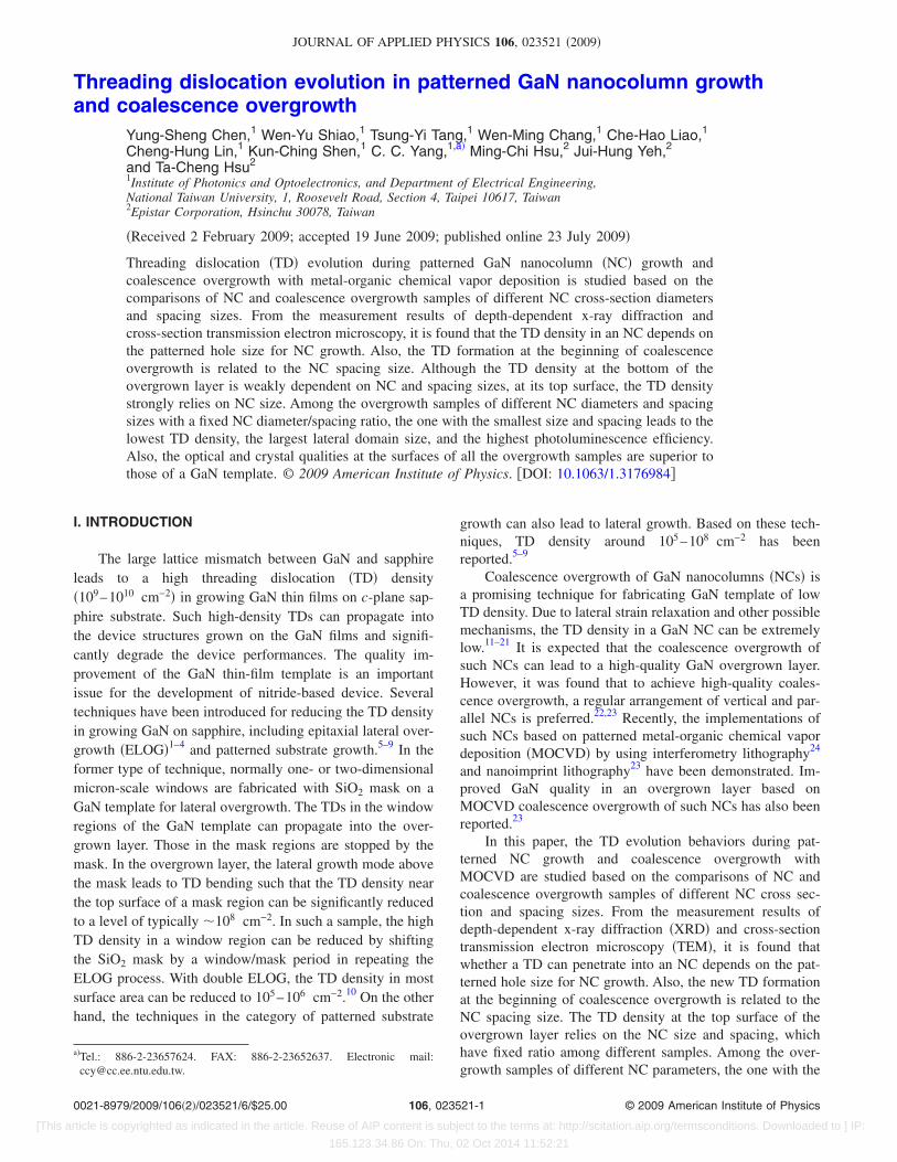
Figure 1 shows three tilted-angle SEM images of NCs ofdifferent cross-sectional sizes, including those of samples �a�A, �b� C, �c� and D, and a cross-section SEM image of �d�sample AO, which illustrates the typical structure of an over-grown sample. Here, one can see a regular arrangement ofhexagonal-shaped NCs in each NC sample. In all samples,the NC heights are all around 1 �m. Also, in each sample,the NC height is quite uniform and the NC top is flat. Thecross-sectional SEM image in Fig. 1�d� clearly shows thelayers of GaN template, SiO2 mask, NC, and overgrowth.The overgrown surfaces of all samples are quite smoothwithout any crack. The pit densities are of the order of107–108 cm−2,23 similar to those of TDs to be discussedbelow. The surface roughness levels of those samples basedon AFM imaging in an area of 5�5 �m2 are shown in TableI. Here, one can see that the roughness level increases withNC size from 0.411 nm of sample AO through 0.665 nm ofsample DO. They are all significantly smaller than that�0.834 nm� of the GaN template �sample E�.
Figure 2 shows the normalized integrated PL intensitiesas functions of temperature of various samples for compari-son. The ratio of the integrated intensity at room temperature
FIG. 1. SEM images of typical NCs in samples A �a�, C �b�, and D �c�, anda typical cross-sectional SEM image of sample AO �d�.
TABLE I. Surface roughness, IQE, and near-surface XRD data of various samples.
Overgrowth sample
Surfaceroughness
�nm�IQE�%�
Screw dislocationdensity�cm−2�
Edge dislocationdensity�cm−2�
Lateral domainsize
��m�
AO/A �250 nm� 0.411 6.7/9.9 3.09�107 5.04�107 2.24BO/B �300 nm� 0.425 4.1/7.1 5.09�107 6.21�107 2.01CO/C �450 nm� 0.473 3.1/4.2 8.11�107 9.24�107 1.73DO/D �600 nm� 0.665 1.6/3.9 9.81�107 1.32�108 1.71E �GaN template� 0.834 1.1 1.09�108 6.63�108 0.81
023521-2 Chen et al. J. Appl. Phys. 106, 023521 �2009�
[This article is copyrighted as indicated in the article. Reuse of AIP content is subject to the terms at: http://scitation.aip.org/termsconditions. Downloaded to ] IP:
165.123.34.86 On: Thu, 02 Oct 2014 11:52:21
over that at 10 K can be regarded as a representation ofinternal quantum efficiency �IQE�, which is related to thedefect density of a sample. In parts �a� and �b�, the compari-sons of integrated PL intensity between the NC samples�A–D� and between the overgrowth samples �AO-DO�, re-spectively, are demonstrated. In each part, the comparisonwith the GaN template �sample E� is also illustrated. TheIQE values of all those samples are listed in Table I. Here,one can see the decreasing IQE trend with increasing NCsize in either NC or overgrowth sample group. In all the NCand overgrowth samples, the IQE values are always higherthan that �1.1%� of the GaN template �sample E�, indicatingthe higher crystal quality of NC growth and coalescenceovergrowth. Also, for each NC size, the IQE value of theovergrowth sample is always lower than that of the corre-sponding NC sample. In other words, new defects can beformed during coalescence overgrowth. With the hole size of250 nm, the NC sample A has an IQE of 9.9%, which is ninetimes that of the GaN template. Also, the correspondingovergrowth sample has an IQE of 6.7%, which is about sixtimes that of the GaN template.
Figure 3 shows the comparisons of screw TD density �a�,edge TD density �b�, and lateral domain size �c� between theovergrowth samples and the GaN template based on depth-dependent XRD measurements. For each parameter above,the GaN template shows a constant value �1.09�108 cm−2
for screw TD density, 6.63�108 cm−2 for edge TD density,and 0.81 �m for lateral domain size� from the surface downto 1.4 �m in depth, beyond which the TD densities increaseand the lateral domain size decreases, indicating that thegrowth quality of the GaN template on sapphire saturates
beyond a growth thickness of about 500 nm. In the over-growth samples, the two TD densities decrease along over-growth thickness and reach the minimum values at thesample surfaces. Also, the lateral domain size increases alongovergrowth thickness. As shown in Fig. 1�d�, the gaps be-tween NCs were partly filled with GaN during the over-growth stage. Among the overgrowth samples, the TD den-sities increase and the lateral domain size decreases withincreasing NC size/spacing. Their values show saturationtrends when overgrowth reaches certain thickness, dependingon the NC size/spacing. A smaller NC size/spacing corre-sponds to a deeper saturating depth or a thinner saturatingovergrowth thickness, implying a more effective coalescenceprocess. When compared with the GaN template, all thethree crystal parameters show improved conditions at theovergrowth surfaces. Comparable edge TD densities andcomparable or slightly larger lateral domain sizes, whencompared with those at the top surface of the GaN template�sample E�, can be observed at the bottoms of the overgrownlayers in the overgrowth samples. However, the screw TDdensities at the bottoms of the overgrown layers in samplesAO-DO are significantly higher than that at the top surface of
FIG. 2. �Color online� �a� Normalized integrated PL intensity vs temperatureof the NC samples A–D and the GaN template �sample E�. �b� Normalizedintegrated PL intensity vs temperature of the overgrowth samples AO-DOand the GaN template �sample E�.
FIG. 3. �Color online� �a� Depth-dependent screw TD densities of samplesAO-DO and E. �b� Depth-dependent edge TD densities of samples AO-DOand E. �c� Depth-dependent lateral domain size of samples AO-DO and E.
023521-3 Chen et al. J. Appl. Phys. 106, 023521 �2009�
[This article is copyrighted as indicated in the article. Reuse of AIP content is subject to the terms at: http://scitation.aip.org/termsconditions. Downloaded to ] IP:
165.123.34.86 On: Thu, 02 Oct 2014 11:52:21
sample E. The lateral domain sizes of the overgrowthsamples increase rapidly from the NC cross-sectional dimen-sions, which are smaller than the level of the GaN template,to the values of 2.76–2.11 times larger at the surfaces �seeTable I�. The most rapid increase in sample AO implies themost effective coalescence process in this sample. The moresignificant reduction in edge TD density �reduced by 3–15times� with NC growth and coalescence overgrowth, whencompared with that of screw TD density �reduced by 1.1–3.5times�, may imply that NC growth can stop the propagationof edge TD more effectively and/or the new TDs formedduring coalescence overgrowth are mainly in the screw type.Nevertheless, in any of the overgrowth samples or the GaNtemplate, the screw TD density is always smaller than theedge TD density. The screw TD densities, edge TD densities,and lateral domain sizes at the surfaces of various samplesare listed in Table I.
IV. TEM STUDIES
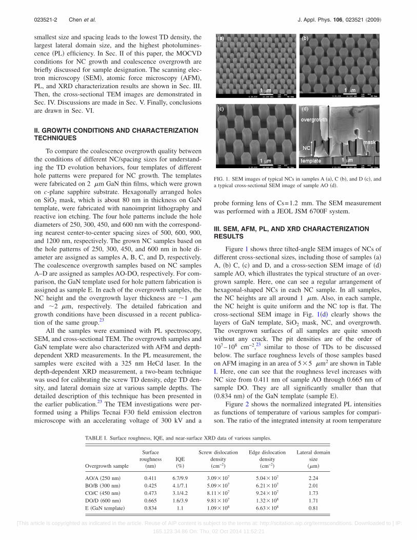
To understand the TD evolution during the growth ofNCs and coalescence overgrowth, cross-section TEM mea-surements were made. Figures 4–6 show TEM images ofsamples A, C, and D, respectively, around the bottom of
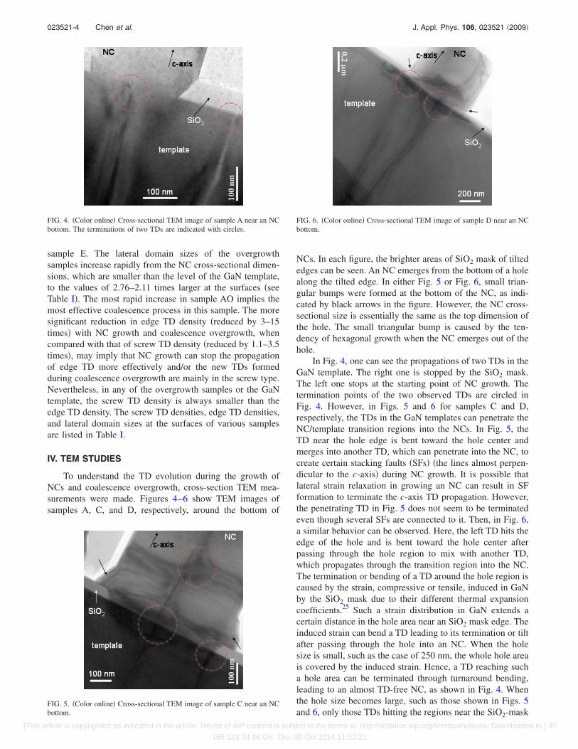
NCs. In each figure, the brighter areas of SiO2 mask of tiltededges can be seen. An NC emerges from the bottom of a holealong the tilted edge. In either Fig. 5 or Fig. 6, small trian-gular bumps were formed at the bottom of the NC, as indi-cated by black arrows in the figure. However, the NC cross-sectional size is essentially the same as the top dimension ofthe hole. The small triangular bump is caused by the ten-dency of hexagonal growth when the NC emerges out of thehole.
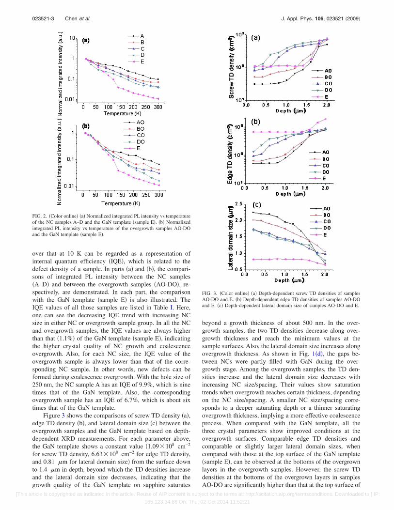
In Fig. 4, one can see the propagations of two TDs in theGaN template. The right one is stopped by the SiO2 mask.The left one stops at the starting point of NC growth. Thetermination points of the two observed TDs are circled inFig. 4. However, in Figs. 5 and 6 for samples C and D,respectively, the TDs in the GaN templates can penetrate theNC/template transition regions into the NCs. In Fig. 5, theTD near the hole edge is bent toward the hole center andmerges into another TD, which can penetrate into the NC, tocreate certain stacking faults �SFs� �the lines almost perpen-dicular to the c-axis� during NC growth. It is possible thatlateral strain relaxation in growing an NC can result in SFformation to terminate the c-axis TD propagation. However,the penetrating TD in Fig. 5 does not seem to be terminatedeven though several SFs are connected to it. Then, in Fig. 6,a similar behavior can be observed. Here, the left TD hits theedge of the hole and is bent toward the hole center afterpassing through the hole region to mix with another TD,which propagates through the transition region into the NC.The termination or bending of a TD around the hole region iscaused by the strain, compressive or tensile, induced in GaNby the SiO2 mask due to their different thermal expansioncoefficients.25 Such a strain distribution in GaN extends acertain distance in the hole area near an SiO2 mask edge. Theinduced strain can bend a TD leading to its termination or tiltafter passing through the hole into an NC. When the holesize is small, such as the case of 250 nm, the whole hole areais covered by the induced strain. Hence, a TD reaching sucha hole area can be terminated through turnaround bending,leading to an almost TD-free NC, as shown in Fig. 4. Whenthe hole size becomes large, such as those shown in Figs. 5and 6, only those TDs hitting the regions near the SiO2-mask
FIG. 4. �Color online� Cross-sectional TEM image of sample A near an NCbottom. The terminations of two TDs are indicated with circles.
FIG. 5. �Color online� Cross-sectional TEM image of sample C near an NCbottom.
FIG. 6. �Color online� Cross-sectional TEM image of sample D near an NCbottom.
023521-4 Chen et al. J. Appl. Phys. 106, 023521 �2009�
[This article is copyrighted as indicated in the article. Reuse of AIP content is subject to the terms at: http://scitation.aip.org/termsconditions. Downloaded to ] IP:
165.123.34.86 On: Thu, 02 Oct 2014 11:52:21
edges are affected by the strain �bending and merging withanother TD�. A TD hitting the central region of a hole canpenetrate into the grown NC. The mechanism ofSiO2-mask-induced strain can well explain the observed TDbehaviors in the transition from the GaN template into anNC. Because all the observed TDs hitting mask edges bendtoward the hole center, it is speculated that GaN in the holeregion is under compressive strain. Therefore, with a largerNC size, the average TD density in the NC becomes higher.This trend is consistent with the conventional ELOGprocess,1–4 in which micron-scale holes �or trenches� andseparations were prepared for overgrowth. In this situation,TDs can easily penetrate into the overgrown layer throughthe large windows, leading to the poor-quality window re-gions and high-quality mask regions in the lateraldimension.1,2 In this sense, a smaller hole size and a smallerNC size are preferred for a lower TD number in an NC.
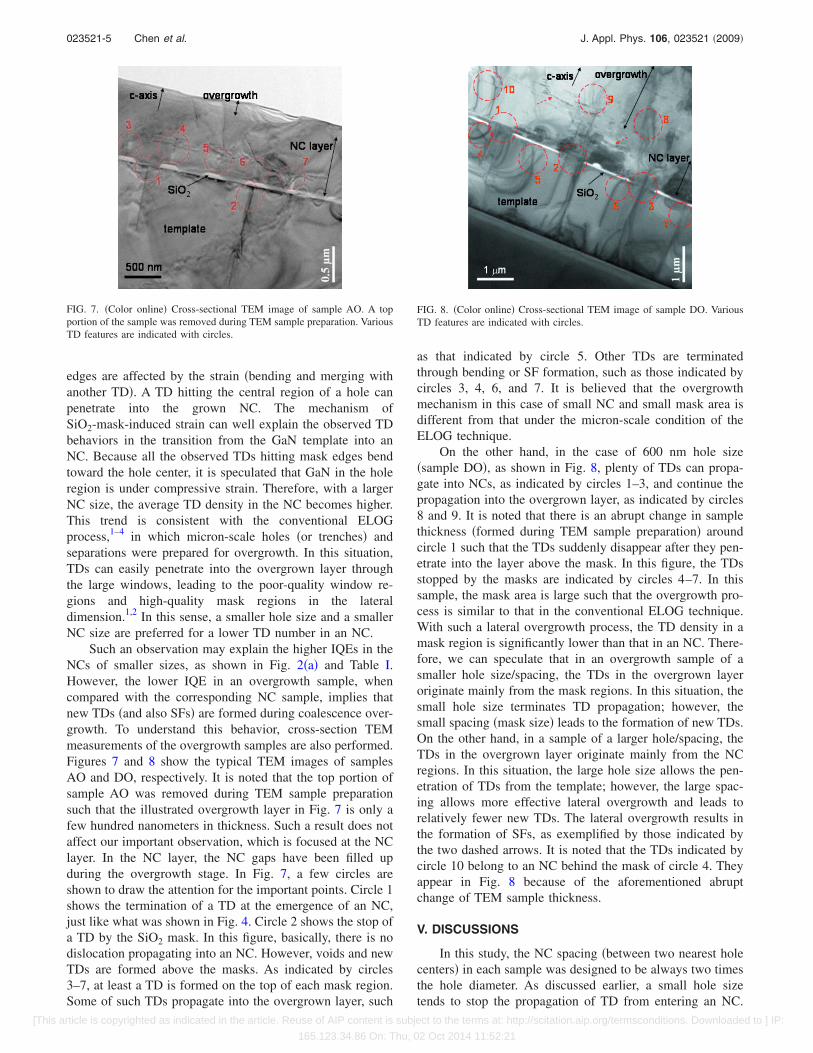
Such an observation may explain the higher IQEs in theNCs of smaller sizes, as shown in Fig. 2�a� and Table I.However, the lower IQE in an overgrowth sample, whencompared with the corresponding NC sample, implies thatnew TDs �and also SFs� are formed during coalescence over-growth. To understand this behavior, cross-section TEMmeasurements of the overgrowth samples are also performed.Figures 7 and 8 show the typical TEM images of samplesAO and DO, respectively. It is noted that the top portion ofsample AO was removed during TEM sample preparationsuch that the illustrated overgrowth layer in Fig. 7 is only afew hundred nanometers in thickness. Such a result does notaffect our important observation, which is focused at the NClayer. In the NC layer, the NC gaps have been filled upduring the overgrowth stage. In Fig. 7, a few circles areshown to draw the attention for the important points. Circle 1shows the termination of a TD at the emergence of an NC,just like what was shown in Fig. 4. Circle 2 shows the stop ofa TD by the SiO2 mask. In this figure, basically, there is nodislocation propagating into an NC. However, voids and newTDs are formed above the masks. As indicated by circles3–7, at least a TD is formed on the top of each mask region.Some of such TDs propagate into the overgrown layer, such
as that indicated by circle 5. Other TDs are terminatedthrough bending or SF formation, such as those indicated bycircles 3, 4, 6, and 7. It is believed that the overgrowthmechanism in this case of small NC and small mask area isdifferent from that under the micron-scale condition of theELOG technique.
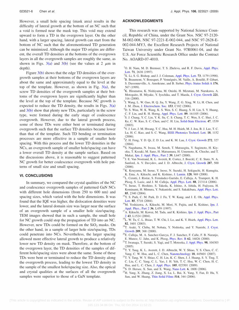
On the other hand, in the case of 600 nm hole size�sample DO�, as shown in Fig. 8, plenty of TDs can propa-gate into NCs, as indicated by circles 1–3, and continue thepropagation into the overgrown layer, as indicated by circles8 and 9. It is noted that there is an abrupt change in samplethickness �formed during TEM sample preparation� aroundcircle 1 such that the TDs suddenly disappear after they pen-etrate into the layer above the mask. In this figure, the TDsstopped by the masks are indicated by circles 4–7. In thissample, the mask area is large such that the overgrowth pro-cess is similar to that in the conventional ELOG technique.With such a lateral overgrowth process, the TD density in amask region is significantly lower than that in an NC. There-fore, we can speculate that in an overgrowth sample of asmaller hole size/spacing, the TDs in the overgrown layeroriginate mainly from the mask regions. In this situation, thesmall hole size terminates TD propagation; however, thesmall spacing �mask size� leads to the formation of new TDs.On the other hand, in a sample of a larger hole/spacing, theTDs in the overgrown layer originate mainly from the NCregions. In this situation, the large hole size allows the pen-etration of TDs from the template; however, the large spac-ing allows more effective lateral overgrowth and leads torelatively fewer new TDs. The lateral overgrowth results inthe formation of SFs, as exemplified by those indicated bythe two dashed arrows. It is noted that the TDs indicated bycircle 10 belong to an NC behind the mask of circle 4. Theyappear in Fig. 8 because of the aforementioned abruptchange of TEM sample thickness.
V. DISCUSSIONS
In this study, the NC spacing �between two nearest holecenters� in each sample was designed to be always two timesthe hole diameter. As discussed earlier, a small hole sizetends to stop the propagation of TD from entering an NC.
FIG. 7. �Color online� Cross-sectional TEM image of sample AO. A topportion of the sample was removed during TEM sample preparation. VariousTD features are indicated with circles.
FIG. 8. �Color online� Cross-sectional TEM image of sample DO. VariousTD features are indicated with circles.
023521-5 Chen et al. J. Appl. Phys. 106, 023521 �2009�
[This article is copyrighted as indicated in the article. Reuse of AIP content is subject to the terms at: http://scitation.aip.org/termsconditions. Downloaded to ] IP:
165.123.34.86 On: Thu, 02 Oct 2014 11:52:21
However, a small hole spacing �mask area� results in thedifficulty of lateral growth at the bottom of an NC such thata void is formed near the mask top. This void may extendupward to form a TD in the overgrown layer. On the otherhand, with a larger spacing, lateral growth can start from thebottom of NC such that the aforementioned TD generationcan be minimized. Although the major TD origins are differ-ent, the overall TD densities at the bottoms of the overgrownlayers in all the overgrowth samples are roughly the same, asshown in Figs. 3�a� and 3�b� �see the values at 2 �m indepth�.
Figure 3�b� shows that the edge TD densities of the over-growth samples at their bottoms of the overgrown layers areabout the same and approximately equal to the level at thetop of the template. However, as shown in Fig. 3�a�, thescrew TD densities of the overgrowth samples at their bot-toms of the overgrown layers are significantly higher thanthe level at the top of the template. Because NC growth isexpected to reduce the TD density, the results in Figs. 3�a�and 3�b� show that plenty new TDs, particularly in the screwtype, were formed during the early stage of coalescenceovergrowth. However, due to the lateral growth process,some of those TDs were either bent or terminated duringovergrowth such that the surface TD densities became lowerthan that of the template. Such TD bending or terminationprocesses are more effective in a sample of smaller holespacing. With this process and the lower TD densities in theNCs, an overgrowth sample of smaller hole/spacing can havea lower overall TD density at the sample surface. Based onthe discussions above, it is reasonable to suggest patternedNC growth for better coalescence overgrowth with hole pat-terns of small size and small spacing.
VI. CONCLUSIONS
In summary, we compared the crystal qualities of the NCand coalescence overgrowth samples of patterned GaN NCswith different hole dimensions �from 250 to 600 nm� andspacing sizes, which varied with the hole dimensions. It wasfound that the IQE was higher, the dislocation densities werelower, and the lateral domain size was larger near the surfaceof an overgrowth sample of a smaller hole size/spacing.TEM images showed that in such a sample, the small holefor NC growth could stop the propagation of TD into an NC.However, new TDs could be formed on the SiO2 masks. Onthe other hand, in a sample of larger hole size/spacing, TDscould penetrate into NCs. Nevertheless, the larger spacingallowed more effective lateral growth to produce a relativelylower new TD density on mask. Therefore, at the bottom ofthe overgrown layer, the TD densities of the samples of dif-ferent hole/spacing sizes were about the same. Some of theseTDs were bent or terminated to reduce the TD density alongthe overgrowth process, leading to the lowest TD density inthe sample of the smallest hole/spacing size. Also, the opticaland crystal qualities at the surfaces of all the overgrowthsamples were superior to those of a GaN template.
ACKNOWLEDGMENTS
This research was supported by National Science Coun-cil, Republic of China, under the Grant Nos. NSC 97-2120-M-002-008, NSC 97-2221-E-002-044, and NSC 97-2628-E-002-044-MY3, the Excellent Research Projects of NationalTaiwan University under Grant No. 97R0061-04, and theU.S. Air Force Scientific Research Office under the ContractNo. AOARD-07-4010.
1O. H. Nam, M. D. Bremser, T. S. Zheleva, and R. F. Davis, Appl. Phys.Lett. 71, 2638 �1997�.
2X. Li, S. G. Bishop, and J. J. Coleman, Appl. Phys. Lett. 73, 1179 �1998�.3B. Beaumont, V. Bousquet, P. Vennéguès, M. Vaille, A. Bouillé, P. Gibart,S. Dassonneville, A. Amokrane, and B. Sieber, Phys. Status Solidi A 176,567 �1999�.
4K. Hiramatsu, K. Nishiyama, M. Onishi, H. Mizutani, M. Narukawa, A.Motogaito, H. Miyake, Y. Iyechika, and T. Maeda, J. Cryst. Growth 221,316 �2000�.
5J. Wang, L. W. Guo, H. Q. Jia, Y. Wang, Z. G. Xing, W. Li, H. Chen, andJ. M. Zhou, J. Electrochem. Soc. 153, C182 �2006�.
6D. S. Wuu, W. K. Wang, K. S. Wen, S. C. Huang, S. H. Lin, S. Y. Huang,C. F. Lin, and R. H. Horng, Appl. Phys. Lett. 89, 161105 �2006�.
7S. J. Chang, Y. C. Lin, Y. K. Su, C. S. Chang, T. C. Wen, S. C. Shei, J. C.Ke, C. W. Kuo, S. C. Chen, and C. H. Liu, Solid-State Electron. 47, 1539�2003�.
8Y. J. Lee, J. M. Hwang, T. C. Hsu, M. H. Hsieh, M. J. Jou, B. J. Lee, T. C.Lu, H. C. Kuo, and S. C. Wang, IEEE Photonics Technol. Lett. 18, 1152�2006�.
9Z. H. Feng, Y. D. Qi, Z. D. Lu, and K. M. Lau, J. Cryst. Growth 272, 327�2004�.
10S. Nagahama, N. Iwasa, M. Senoh, T. Matsusgita, Y. Sugimoto, H. Kiy-oku, T. Kozaki, M. Sano, H. Matsumura, H. Umemoto, K. Chocho, and T.Mukai, Jpn. J. Appl. Phys., Part 2 39, L647 �2000�.
11J. E. Van Nostrand, K. L. Averett, R. Cortez, J. Boeckl, C. E. Stutz, N. A.Sanford, A. V. Davydov, and J. D. Albrecht, J. Cryst. Growth 287, 500�2006�.
12K. Kouyama, M. Inoue, Y. Inose, N. Suzuki, H. Sekiguchi, H. Kunugita,K. Ema, A. Kikuchi, and K. Kishino, J. Lumin. 128, 969 �2008�.
13L. Cerutti, J. Ristiæ, S. Fernández-Garrido, E. Calleja, A. Trampert, K. H.Ploog, S. Lazic, and J. M. Calleja, Appl. Phys. Lett. 88, 213114 �2006�.
14Y. Inoue, T. Hoshino, S. Takeda, K. Ishino, A. Ishida, H. Fujiyasu, H.Kominami, H. Mimura, Y. Nakanishi, and S. Sakakibara, Appl. Phys. Lett.85, 2340 �2004�.
15Y. S. Park, C. M. Park, D. J. Fu, T. W. Kang, and J. E. Oh, Appl. Phys.Lett. 85, 5718 �2004�.
16M. Yoshizawa, A. Kikuchi, M. Mori, N. Fujita, and K. Kishino, Jpn. J.Appl. Phys., Part 2 36, L459 �1997�.
17A. Kikuchi, M. Kawai, M. Tada, and K. Kishino, Jpn. J. Appl. Phys., Part2 43, L1524 �2004�.
18L. W. Tu, C. L. Hsiao, T. W. Chi, I. Lo, and K. Y. Hsieh, Appl. Phys. Lett.82, 1601 �2003�.
19T. Araki, Y. Chiba, M. Nobata, Y. Nishioka, and Y. Nanishi, J. Cryst.Growth 209, 368 �2000�.
20E. Calleja, M. A. Sanchez-Garcya, F. J. Sanchez, F. Calle, F. B. Naranjo,E. Munoz, U. Jahn, and K. Ploog, Phys. Rev. B 62, 16826 �2000�.
21T. Iwanaga, T. Suzuki, S. Yagi, and T. Motooka, J. Appl. Phys. 98, 104303�2005�.
22T. Y. Tang, K. L. Averett, J. D. Albrecht, W. Y. Shiao, Y. S. Chen, C. C.Yang, C. W. Hsu, and L. C. Chen, Nanotechnology 18, 445601 �2007�.
23T. Y. Tang, W. Y. Shiao, C. H. Lin, K. C. Shen, J. J. Huang, S. Y. Ting, T.C. Liu, C. C. Yang, C. L. Yao, J. H. Yeh, T. C. Hsu, W. C. Chen, H. C.Hsu, and L. C. Chen, J. Appl. Phys. 105, 023501 �2009�.
24S. D. Hersee, X. Sun, and X. Wang, Nano Lett. 6, 1808 �2006�.25H. Yang, X. Zhang, Z. Jiang, X. Lu, L. Bai, X. Yang, Y. Fan, D. Hu, Y.
Sun, and W. Huang, Thin Solid Films 514, 344 �2006�.
023521-6 Chen et al. J. Appl. Phys. 106, 023521 �2009�
[This article is copyrighted as indicated in the article. Reuse of AIP content is subject to the terms at: http://scitation.aip.org/termsconditions. Downloaded to ] IP:
165.123.34.86 On: Thu, 02 Oct 2014 11:52:21