thin film precursors, properties and applications ... · thin film precursors, ... simulation...
TRANSCRIPT
Thin Film Precursors, Properties and Applications: Chemical Vapour Deposition and Atomic Layer Deposition
of Group 4, 11 and 13 Elements and Their Oxides
by
Peter George Gordon
A thesis submitted to the Faculty of Graduate and Postdoctoral Affairs in partial fulfilment of the requirements for the degree of
Doctor of Philosophy
in
Chemistry
Carleton UniversityOttawa, Ontario
Canada
August 2013
© 2013, Peter George Gordon
Abstract
Brass and bronze substrates were coated by atomic layer deposition (ALD) with
alumina and titania in small and large scale batches. These films were evaluated for use
as protective and cosmetic coatings. Optimization of deposition parameters for uniform
coatings both on individual coins and across a batch for Al2O3 and TiO2 films was
performed. The effect of film thickness on colour was examined. High-quality, uniform
coatings were achieved with multi-pulse programs.
The interference colours resulting from thin films of Al2O3 deposited by ALD on
silicon were analyzed using a robotic gonioreflectometer. A series of thin films were
deposited and their reflectivity values obtained for the visible spectrum. A comparison of
these values with the predictions of computer simulations has revealed deviations from
predicted reflectivities. The effect of these discrepancies on perceived colour appearance
was investigated. Simulation predicts larger iridescence than what was observed.
Alumina films were deposited by ALD on flat and nanostructured silicon substrates,
and incorporated into PEDOT-Al2O3-silicon architectures that were then evaluated as
photovoltaic devices. The reverse saturation currents observed on flat devices made with
Al2O3 films were similar devices made with an SiO2 layer. The structured samples with
Al2O3 showed a considerable increase in efficiency (of up to five times) over the
equivalent flat samples.
A new indium(III) guanidinate, (In[(NiPr)2CNMe2]3, was synthesized.
Thermogravimetric analysis showed elemental indium was produced from the compound
as a residual mass. Thermolysis in a sealed NMR tube showed carbodiimide and
ii
protonated dimethyl amine by 1H NMR. Chemical vapour deposition (CVD) experiments
above 275 °C with air as the reactant gas produced cubic indium oxide films with good
transparency.
Dimeric silver(I) and gold(I) tert-butyl-imino-2,2-dimethylpyrrolidinates were
synthesized and evaluated for thermal stability by thermal gravimetric analysis,
differential scanning calorimetry and variable-temperature solution NMR. The
compounds were used to deposit metallic films on silicon and glass substrates by CVD,
with and without a flow of heated nitrogen gas. The compounds decomposed to produce
metallic films at 140 °C for the silver compound and 300 °C for the gold compound.
Additional CVD experiments with heated nitrogen gas flow improved film uniformity
without sacrificing film purity.
iii
Preface
This preface provides full bibliographical details for each article included in this thesis, as well as whether the article is reproduced in whole or in part. Use of copyrighted material is likewise acknowledged here. When citing material from this thesis, please cite both the thesis and the article relevant to the chapter, if the chapter is based on a publication.
Pursuant to the Integrated Thesis policy of Carleton University, the “supervisor” (Seán T. Barry) and the “student” (Peter G. Gordon) confirm that the student was fully involved in setting up and conducting the research, obtaining data and analyzing results, as well as preparing and writing the material presented in the co-authored article(s) integrated in the thesis. Additionally, the supervisor confirms the information provided by the student in this preface.
Chapter 1
Figure 1.5 is reprinted with permission from the American Institute of Physics.
Chapter 3
Gordon, P. G.; Baribeau, R.; Barry, S. T.; Goniocolorimetric Study of Aluminum Oxide Films Deposited by Atomic Layer Deposition, Thin Solid Films, 2012, 520, 2943.
The article is wholly reproduced and edited for formatting and clarity of presentation.
The student performed all work related to deposition and characterization of films (with the exception of goniocoloureflectometry) and simulations. Writing was collaborative between all co-authors.
Chapter 4
Demtchenko, S.; McGarry, S.; Gordon, P. G.; Barry, S. T.; Tarr, N. G.; Characterization and assessment of a novel hybrid organic/inorganic metal-insulator-semiconductor structure for photovoltaic applications, Proc.SPIE 7750, 2010, DOI 10.1117/12.871360.
The article is wholly reproduced and edited for formatting and clarity of presentation.
The student performed all work related to deposition of alumina films and thickness characterization. Writing was collaborative between all co-authors.
Chapter 5
Gordon, P. G.; Ward, M. J.; Heikkila, M. J.; Monillas, W. H.; Yap, G. P. A.; Ritala, M.; Leskelä, M.; Barry, S. T.; Chemical Vapour Deposition of In2O3 Thin Films from a tris-
Guanidinate Indium Precursor, Dalton Trans., 2011, 40, 9425.
The article is wholly reproduced and edited for formatting and clarity of presentation.
The student performed all work related to synthesis of precursors, deposition of films, thickness characterization, SEM and resistance measurements. Writing was collaborative between all co-authors.
iv
Chapter 6
Coyle, J. P.; Gordon, P. G.; Wells, A. P.; Sirianni, E. R.; Yap, G. P. A.; Barry, S. T.; Thermally Robust Gold and Silver Iminopyrrolidinates for Chemical Vapour Deposition of Metal Films, Chem. Mater., 2013, submitted. Manuscript ID: cm-2013-02658c.
Chapter 6 includes data presented in the as-yet unpublished manuscript referenced above, as well as additional unreported Ag and Au CVD data. J.P. Coyle is the corresponding author for the submitted manuscript.
The student performed all work related to deposition of metal films (with the exception of gold depositions without nitrogen flow), thickness characterizations, resistance measurements and SEM imaging.
v

Acknowledgements
It is a pleasure to thank the many people who made the long road to this thesis not
only possible, but thoroughly enjoyable.
It is difficult to overstate my gratitude to my Ph.D. supervisor, Dr. Seán T. Barry. The
extent to which I understand chemistry can in large part be attributed to his generosity,
knack for explaining things clearly and simply, and his willingness to let me pursue my
own path. Throughout my return to graduate studies, he provided encouragement, sound
advice, good teaching, interesting challenges, amazing opportunities, and friendship.
I am indebted to my many Barry Lab student colleagues for providing untold hours of
thoughtful discussion and foolish shenanigans in nearly equal measure. In roughly
chronological order I would especially like to thank Allison Brazeau, Yamile Wasslen,
Julie Delahunt, Jason Coyle, Agnieszka Kurek and Peter Pallister. From my increasingly
distant undergraduate years, I would like to thank Mark Flumiani for helping me stumble
through the first leg of this journey, and for his enduring friendship.
I would like to thank the staff and faculty of the Chemistry Department at Carleton. I
will always remain amazed at my good fortune to have worked with such a great group of
people.
I would like to thank my extended family for their unrelenting support. In particular I
would like to thank my step-parents Joseph Smarkala and Nancy Gordon, both for
supporting me in my schooling and for the love and support they have provided my
parents over the years.
I could never thank Erin Christine Sallie enough for her depth of patience, generosity,
and life-changing love. I am not sure I could have made it this far without her. She is the
heart of my heart.
Lastly, and most importantly, I wish to thank my loving parents, Susan Lynne
Smarkala and Donald Davey Gordon. They created me, raised me, taught me to cultivate
my curiosity (among a great many other things), and always supported me without
question. It is to them that I dedicate this thesis.
vi
Table of Contents
Abstract...............................................................................................................................2
Preface.................................................................................................................................4
Acknowledgements............................................................................................................6
Table of Contents...............................................................................................................7
Chapter 1 - Introduction..................................................................................................1
1.1 Chemical Vapour Deposition and Atomic Layer Deposition...........................................1
1.2 ALD for Protective and Cosmetic Coatings ..................................................................11
1.3 Photovoltaic Devices.....................................................................................................17
Chapter 2 - Protective and Cosmetic Coatings for Coinage Metals and Their Alloys
............................................................................................................................................21
2.1 Abstract.........................................................................................................................21
2.2 Introduction...................................................................................................................21
2.3 Results and Discussion..................................................................................................23
2.4 Experimental.................................................................................................................35
2.5 Conclusions...................................................................................................................39
Chapter 3 - Goniocolorimetric Study of Aluminum Oxide Films Deposited by
Atomic Layer Deposition.................................................................................................41
3.1 Abstract.........................................................................................................................41
3.2 Introduction...................................................................................................................42
3.3 Experimental.................................................................................................................43
3.4 Results and Discussion..................................................................................................47
3.5 Conclusions...................................................................................................................63
vii
Chapter 4 - Characterization and assessment of a novel hybrid organic/inorganic
metal-insulator-semiconductor structure for photovoltaic applications.....................64
4.1 Abstract.........................................................................................................................64
4.2 Introduction...................................................................................................................65
4.3 Experimental.................................................................................................................68
4.4 Results and Discussion..................................................................................................71
4.5 Future Work...................................................................................................................77
4.6 Acknowledgements.......................................................................................................78
Chapter 5 - Chemical vapour deposition of In2O3 thin films from a tris-guanidinate
indium precursor.............................................................................................................79
5.1 Abstract.........................................................................................................................79
5.2 Results and Discussion..................................................................................................80
5.3 Thermolysis ..................................................................................................................85
5.4 Film depositions and characterization...........................................................................87
5.5 Experimental.................................................................................................................96
5.6 Conclusions.................................................................................................................100
Chapter 6 - Metallic Silver and Gold Chemical Vapour Deposition from Novel
Precursors.......................................................................................................................102
6.1 Abstract.......................................................................................................................102
6.2 Introduction.................................................................................................................103
6.3 Results and Discussion................................................................................................105
6.4 Experimental...............................................................................................................127
6.5 Conclusion...................................................................................................................135
Chapter 7 - Conclusions...............................................................................................138
viii
References.......................................................................................................................143
List of Tables
Table 2.1 Single-point thickness measurements of film thickness on bronze and silicon
substrates as measured by ellipsometry. The last row indicates the percentage difference
in observed values for the two substrates..........................................................................24
Table 2.2 Pulse program timing used in the bulk ALD experiments for alumina and
titania coatings. Each row represents a single ALD cycle, yielding a monolayer of target
material. The metal precursors are represented by "M" and all values are in seconds. ....38
Table 4.1 Voltage intercepts from the V-C characterization of flat MIS devices with SiO2
insulator showing increasing barrier height with increasing oxidation temperature.........73
Table 4.2 Predicted parameters of the optimized flat MIS device with SiO2 insulator and
PEDOT as the metal...........................................................................................................75
Table 5.1 Selected crystal data and structure refinement parameters for compound 1....82
Table 5.2 Selected bond lengths and angles for compound 1..........................................83
Table 5.3 The various deposition runs undertaken using different masses of 1 as the
precursor and air as the reactant gas..................................................................................88
Table 6.1 Selected bond lengths and angles for 1 and 2.................................................107
ix
List of Figures
Figure 1.1 Various CVD apparatus configurations............................................................3
Figure 1.2 Thermal decomposition routes available to copper guanidinates (analogous
routes available to amidinates).............................................................................................7
Figure 1.3 2,2-diethyl-tertbutyl-iminopyrrolidine described and studied in Chapter 6,
highlighting features that prevent decomposition routes observed for amidinate and
guanidinate analogs..............................................................................................................7
Figure 1.4 Schematic of the ALD process: a) the first precursor is introduced and a
monolayer is formed; b) an N2 purge and evacuation removes remaining precursor and
volatile side products; c) the second precursor is introduced and reacts with the first
monolayer, forming the first monolayer of the target film; d) another N2 purge and
evacuation removes remaining precursor and volatile side products. e) The process is
repeated until the desired thickness is reached. ..................................................................9
Figure 1.5 Table summarizing materials grown by ALD. Reprinted with permission
from American Institute of Physics.124 Copyright 2013, AIP Publishing LLC..................10
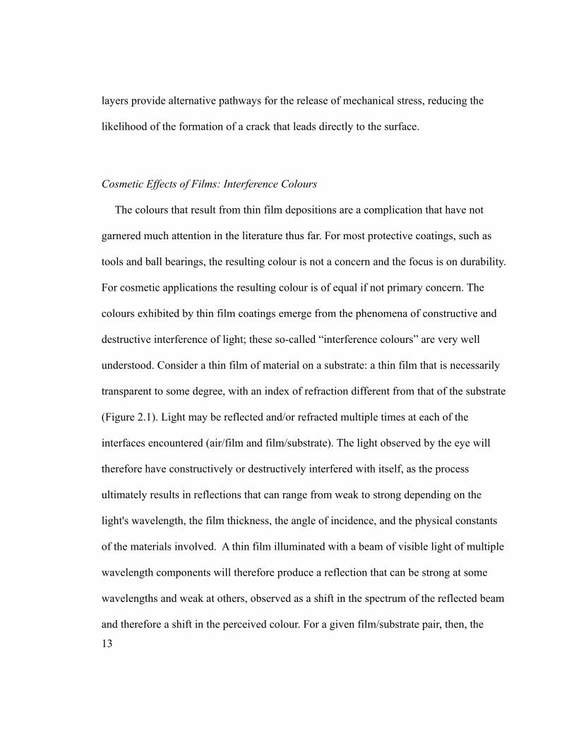
Figure 1.6 Model illustrating the origin of interference colours. A is an incident beam of
light at a specific frequency. Due to partial reflection, it splits into beam C and B.
Depending upon the thickness of the film (d) and the angle of incidence of A, the path
length C+D may alter the phase of E with respect to B. Constructive or destructive
interference may then occur, altering the wavelength of the outgoing light. The refractive
indices of the materials are given by n1, n2 and n3.............................................................14
Figure 1.7 Representation of the CIELab coordinate system for describing colour. .......16
x
Figure 1.8 Band structure diagram for a Schottky barrier diode. EC is the conduction
band, EF the Fermi level, and EV the valence band. ..........................................................18
Figure 2.1 An uncoated coin (b) is contrasted against a coin with a 1000 Å alumina
coating (a) and a coin with a 1500 Å coating (c). .............................................................24
Figure 2.2 Acetamidinato alkyl aluminum precursor employed in this work..................24
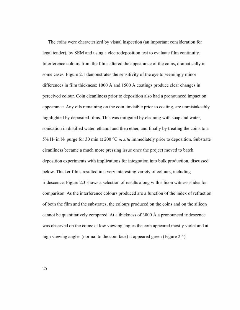
Figure 2.3 Deposition series showing coins in the top two rows and their respective
silicon witness slides at the bottom. From left to right, each column presents coatings of
1000 Å, 3000Å, 8000 Å and 10,000 Å. The second witness slide is shown at two different
viewing angles to demonstrate its iridescence, while the last slide exhibits delamination.
Note that this delamination was observed to a much lesser degree on the coin. ..............26
Figure 2.4 Iridescence of 3000 Å film of Al2O3 on bronze. ............................................27
Figure 2.5 SEM image of a coin coated with 1000 Å Al2O3, after electrodeposition
experiment. Copper metal (white) indicates a flaw in the film exposing the coin to the
electrodeposition solution. ................................................................................................28
Figure 2.6 Thickness results for three pulse programs, revealing uniformity throughout
the volume of a single batch run. Error bars depict standard deviations (evaluated across
all eleven samples) of 72 Å, 20 Å and 10 Å for the single, double and triple pulse
program thickness measurements respectively. Image at right depicts the placement of
witness slides used for ellipsometric thickness measurements. Racks without witnesses
are not shown but were present and fully loaded...............................................................32
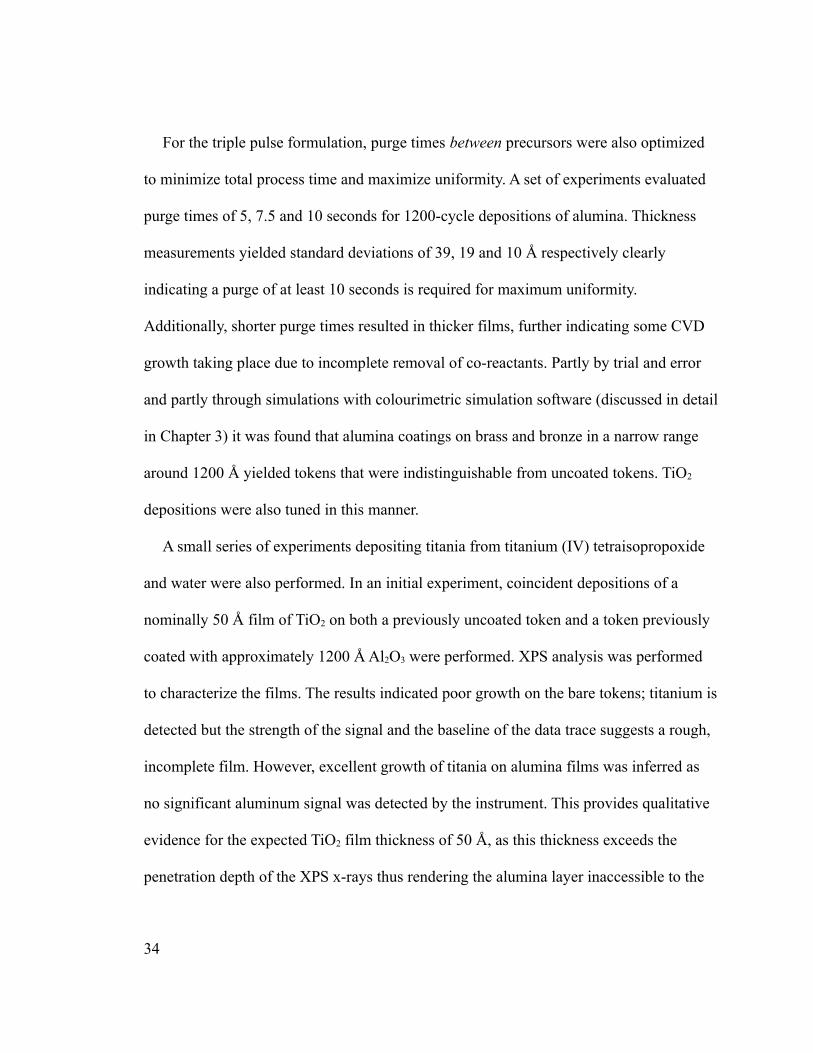
Figure 2.7 XPS spectra of a bare token exposed to a TiO2 ALD process (a) and a token
with a 1200 Å Al2O3 coating exposed to the same TiO2 ALD process (b). The shape of the
xi
baseline in a suggests a rough surface. Note that no aluminum oxide process was applied
to sample a; the Al signal is marked there for comparison with b. ...................................35
Figure 2.8 Custom-built ALD tool schematic..................................................................36
Figure 2.9 Empty coin racks (left) and filled, after deposition (right). Note the variation
in interference colour on the coins and racks, clearly indicating non-uniform thickness..38
Figure 3.1 Acetamidinato alkyl aluminum precursor employed in this work. ................43
Figure 3.2 Schematic of the atomic layer deposition system. .........................................44
Figure 3.3 The goniorelflectometer used to collect reflectance data...............................47
Figure 3.4 Experimental data (a) and calculated data (b) of the reflectance of films of
various thicknesses with a viewing angle of 10°...............................................................49
Figure 3.5 Experimental and calculated regular reflectance of a 459 Å film over the
visible range of light at various viewing angles.................................................................50
Figure 3.6 Plot of percent difference between experimental and calculated values for
reflectance against wavelength and viewing angle for a bare silicon (100) wafer. Note that
the topographical scale is in the range −2 to +2%.............................................................51
Figure 3.7 Plot of percent difference between experimental and calculated values for
reflectance against wavelength and viewing angle for a 1613 Å Al2O3 film on a silicon
(100) wafer. Note that the topographical scale is much larger than in Figure 3.6, ranging
from −25% to +90%..........................................................................................................52
Figure 3.8 Reflectivity calculations for a 459 Å aluminum oxide film on silicon using a)
the bulk dispersion curve for aluminum oxide and b) the dispersion curve as measured
experimentally for an aluminum oxide film deposited by ALD........................................54
xii
Figure 3.9 a*b* CIELAB (CIE D65) plots of (a) observed and (b) calculated data for
selected film thicknesses over a range of viewing angles. Coloured axes are approximate
representations of the CIELAB space to help guide the eye.............................................55
Figure 3.10 a*b* CIELAB (CIE D65) plots comparing +/- 5% error estimates for (a)
908 Å and (b) 1613 Å films with observed data. Each point corresponds to a viewing
angle. .................................................................................................................................61
Figure 4.1 Representations of the hybrid MIS device. Flat device is shown in (a),
nanostructured device shown in (b) and band diagram in (c). ..........................................68
Figure 4.2 Processing and testing of devices: (a) 2’’ wafer of devices (b) testing of an
individual device under the solar simulator.......................................................................71
Figure 4.3 I-V characteristics of flat MIS devices with SiO2 (a) full dark IV curves (b)
dark reverse saturation current...........................................................................................72
Figure 4.4 Illuminated I-V characteristic of an MIS device with no intentional oxide; (a)
measured under a solar simulator (b) measured under a halogen lamp with a sintered back
contact and a non-sintered contact.....................................................................................74
Figure 4.5 I-V curves for flat MIS devices with Al2O3 insulator (a) in the dark and (b)
under illumination..............................................................................................................76
Figure 4.6 Nanostructured MIS devices; (a) SEM image of surface structuring and (b)
relative power conversion efficiency of a set of structured and flat MIS devices processed
in parallel with 8 Å Al2O3 insulator....................................................................................77
xiii
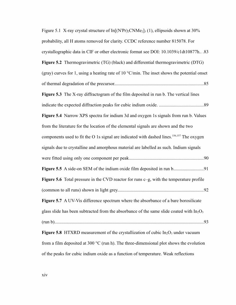
Figure 5.1 X-ray crystal structure of In[(NiPr)2CNMe2]3 (1), ellipsoids shown at 30%
probability, all H atoms removed for clarity. CCDC reference number 815078. For
crystallographic data in CIF or other electronic format see DOI: 10.1039/c1dt10877h.. .83
Figure 5.2 Thermogravimetric (TG) (black) and differential thermogravimetric (DTG)
(gray) curves for 1, using a heating rate of 10 °C/min. The inset shows the potential onset
of thermal degradation of the precursor.............................................................................85
Figure 5.3 The X-ray diffractogram of the film deposited in run b. The vertical lines
indicate the expected diffraction peaks for cubic indium oxide. ......................................89
Figure 5.4 Narrow XPS spectra for indium 3d and oxygen 1s signals from run b. Values
from the literature for the location of the elemental signals are shown and the two
components used to fit the O 1s signal are indicated with dashed lines.156,157 The oxygen
signals due to crystalline and amorphous material are labelled as such. Indium signals
were fitted using only one component per peak................................................................90
Figure 5.5 A side-on SEM of the indium oxide film deposited in run b..........................91
Figure 5.6 Total pressure in the CVD reactor for runs c–g, with the temperature profile
(common to all runs) shown in light grey..........................................................................92
Figure 5.7 A UV-Vis difference spectrum where the absorbance of a bare borosilicate
glass slide has been subtracted from the absorbance of the same slide coated with In2O3
(run b).................................................................................................................................93
Figure 5.8 HTXRD measurement of the crystallization of cubic In2O3 under vacuum
from a film deposited at 300 °C (run h). The three-dimensional plot shows the evolution
of the peaks for cubic indium oxide as a function of temperature. Weak reflections
xiv
observed at room temperature and at the highest temperature originate from the sample
holder. ................................................................................................................................95
Figure 5.9 CVD apparatus used for the deposition of indium oxide from 1 and air........99
Figure 6.1 Amidinates, guanidinates, and iminopyrrolidinates ligands used in precursors
for CVD and ALD (R, R’ = any alkyl group)..................................................................105
Figure 6.2 Synthesis of silver(I) and gold(I) tert-butyl-imino-2,2-dimethylpyrrolidinate.
..........................................................................................................................................106
Figure 6.3 Molecular diagram of 2 with thermal ellipsoids at 30% probability. Hydrogen
atoms omitted for clarity. Ag analogue compound 1 is isomorphic with 2. ...................108
Figure 6.4 Thermogravimetric analysis of 1 (black) and 2 (gray). Experiments were run
under 1 atm nitrogen with a ramp rate of 10 °C/min. Sample size for 1 and 2 were 10.49
mg and 13.65 mg, respectively. Note that the maximum percentage residual mass of pure
metal for 1 and 2 would be 39.35 % and 54.23 % respectively. .....................................109
Figure 6.5 Isothermal TGA of (a) 1 and (b) 2. Isothermal temperatures, indicated in the
right hand legend (°C), were reached at a rate of 40 °C/min. Sample sizes were between
3.10 mg and 3.67 mg. ......................................................................................................110
Figure 6.6 Differential scanning calorimetry of 1, 2, and 3 in hermetically sealed
aluminum pans. Temperature ramp was 10 °C/min up to 325 °C. Sample masses were
1.066 mg, 1.625 mg, and 3.790 mg for 1, 2, and 3, respectively. Exotherms are up.......112
Figure 6.7 Evaporation kinetics of 1 (♦), 2 (■) and 3 (●)..............................................114
Figure 6.8 Decomposition of 1 and 2 in solution (C6D6) measured by 1H NMR...........116
xv
Figure 6.9 Film thicknesses measured from the CVD of 1 (bottom) and 2 (top) at
different furnace temperatures. Depositions with 1 consumed 50 - 60 mg of compound.
Depositions for 2 consumed varying amounts: 13.9 mg (300 °C); 21.8 mg (350 °C); 5.9
mg (400 °C); 20.6 mg (450 °C); 23.5 (500 °C)...............................................................119
Figure 6.10 SEM images for thin films deposited without N2 flow from (a, b) 1 and (c,
d) 2 at 200 °C and 350 °C, respectively. Images from the CVD of 1 were measured (a)
0.75 cm and (b) 7.75 cm from the precursor inlet. Images from the CVD of 2 were
measured (c) 5 cm and (d) 11 cm from the precursor inlet. Film thicknesses in a, b, and c
are approximately 87 nm, 23 nm and 123 nm respectively. A reliable film thickness
measurement for d could not be obtained. ......................................................................120
Figure 6.11 Temperature series for silver CVD from 1 with nitrogen flow. .................122
Figure 6.12 Film thicknesses for Ag CVD from 1 with heated N2 flow, measured by
AFM. ...............................................................................................................................123
Figure 6.13 Thickness profile for Ag CVD at 300 °C, with nitrogen flow, comparing
values obtained by SEM and AFM. ................................................................................124
Figure 6.14 Comparison of CVD growth of gold from 2, with (dotted lines) and without
(solid lines) nitrogen flow. The triangular data points depict the temperature gradient of
the furnace tube. Intermediate temperatures of 350 °C and 400 °C (not shown) result in
similar, intermediate growth. ..........................................................................................126
Figure 6.15 CVD apparatus with attachment for heated nitrogen delivery. Dotted lines
indicate the three separately-controlled heating zones. ..................................................132
xvi
Figure 6.16 Example of histogram technique used to determine film thickness from
AFM data. Data shown is from a gold deposition from 2 at 350 °C, 8 cm from the
precursor inlet..................................................................................................................134
xvii
Chapter 1 - Introduction
This chapter provides an introduction to the central theoretical and practical concepts
addressed herein. The overarching theme in this work is the chemistry and practical
applications of thin film depositions. The characterization of both the deposited films and
the precursors used to create the films will be addressed. Two techniques for film
deposition were studied: Chemical Vapour Deposition (CVD) and Atomic Layer
Deposition (ALD). Both techniques are based on similar fundamentals regarding optimal
precursor design and have similar process parameters, but there are very important
differences.
1.1 Chemical Vapour Deposition and Atomic Layer Deposition
Chemical Vapour Deposition
Chemical vapour deposition (CVD) is a gas-phase thin film deposition method in
which a chemical precursor is entrained in a continuous flow over a substrate. This
precursor or a reactive intermediate then chemisorbs on the surface. Co-reactant gasses
such as oxygen or nitrogen may also be introduced to assist in forming oxides or nitrides,
for example. The driving energy for the chemistry at the surface can be supplied in a
variety of ways including electrical discharge, exposure to light, or exposure to heat. The
focus here will be on thermal processes. For clean films with high growth rates there are
several criteria that CVD precursors (or their reactive intermediates) must meet. They
must not react or decompose in the gas phase to produce unreactive species or particulate
1
material (unless this is the intent). Such terminal reactions in the gas phase lead to poor
film coverage and poor film adhesion. Steric bulk and low molecular weight are ideal for
high volatility at low temperatures, which keeps the energy demands of the system low.
Halides are avoided as they tend to get incorporated into films as impurities, potentially
altering the desired electrical properties even at very low concentrations.1 More broadly,
undesirable contaminants should in general be excluded from precursor design where
possible. As an example, it is best to avoid oxygen-containing precursors if your target
film is a nitride, as undesirable precursor decomposition may result in impurities.
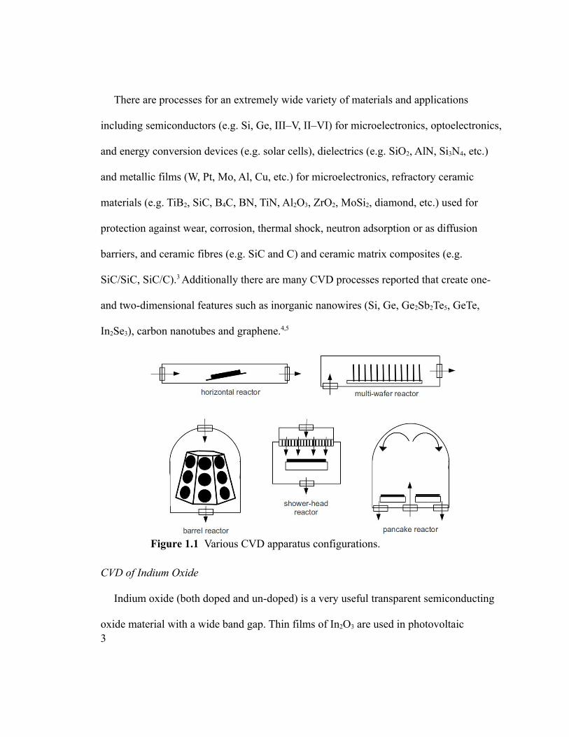
The path and nature of mass transport, i.e. the manner in which the precursor is
delivered to the substrate, has a large impact on the uniformity of the resulting film (or
films, where multiple individual substrates are coated in the same experiment). Several
reactor designs are used; some common examples are illustrated below (Figure 1.1). In
each, the same processes are at work at the substrate surface: diffusion and adsorption of
precursor, surface diffusion and reactions of adsorbed species, desorption and diffusion of
volatile reaction products, and film growth. Operating pressures vary from tens of mTorr
to 1 atm and reactor temperatures vary from room temperature to 1500 K.2 Because film
growth is dependent upon substrate orientation as well as heat and mass flow, different
CVD reactors may yield significantly different results under otherwise identical
conditions. Each process must be tuned to a given reactor; even on the same apparatus
repeatability can be elusive without proper attention to detail.
2
There are processes for an extremely wide variety of materials and applications
including semiconductors (e.g. Si, Ge, III–V, II–VI) for microelectronics, optoelectronics,
and energy conversion devices (e.g. solar cells), dielectrics (e.g. SiO2, AlN, Si3N4, etc.)
and metallic films (W, Pt, Mo, Al, Cu, etc.) for microelectronics, refractory ceramic
materials (e.g. TiB2, SiC, B4C, BN, TiN, Al2O3, ZrO2, MoSi2, diamond, etc.) used for
protection against wear, corrosion, thermal shock, neutron adsorption or as diffusion
barriers, and ceramic fibres (e.g. SiC and C) and ceramic matrix composites (e.g.
SiC/SiC, SiC/C).3 Additionally there are many CVD processes reported that create one-
and two-dimensional features such as inorganic nanowires (Si, Ge, Ge2Sb2Te5, GeTe,
In2Se3), carbon nanotubes and graphene.4,5
Figure 1.1 Various CVD apparatus configurations.
CVD of Indium Oxide
Indium oxide (both doped and un-doped) is a very useful transparent semiconducting
oxide material with a wide band gap. Thin films of In2O3 are used in photovoltaic 3
devices,6 electro-optical devices,7,8 anti-reflection coatings,9 and as a sensor of various
oxidizing gases.10–12 Amorphous and crystalline indium oxide has been previously
prepared by evaporation and sputtering,13 spray pyrolysis,14 atomic layer deposition (ALD
),15,16 thermal oxidation, ion assisted deposition, pulsed laser deposition,17 and various
forms of chemical vapour deposition (CVD ).18,19 Deposition temperatures range from as
low as 100 °C to 450 °C, and resistivities from as low as 2.74 mΩ·cm have been
reported.20,15
As mentioned above, thermal CVD is a relatively fast and straightforward way to
deposit thin, smooth and conformal films on the nanometre to micrometre scale. The
CVD of indium oxide has previously been studied using trimethyl indium (In(CH3)3) and
triethyl indium (In(CH2CH3)3),21 indium aminoalcohols and ketoimines,22 indium 2,2,6,6-
tetramethyl-3,5-heptanedionate (In(thd)3) and indium acetylacetonates (In(acac)3),23 and
indium alkoxides (In(OR)3).24 Chapter 5 presents work on the synthesis of the indium
guanidinate precursor In[(NiPr)2CNMe2]3 and an evaluation of this compound in the
thermal CVD deposition of indium oxide thin films. The precursor's suitability for use in
gas-phase deposition was evaluated using bench top melting point determination,
thermogravimetric analysis (TGA ), differential scanning calorimetry (DSC ), and NMR
thermolysis studies. Films were analyzed by ellipsometry, IR and UV-Vis spectroscopy,
x-ray diffraction (XRD), scanning electron microscopy (SEM), energy-dispersive x-ray
spectroscopy (EDS) and x-ray photoelectron spectroscopy (XPS). To our knowledge, this
is the first time an indium guanidinate species has been used for CVD.
4
Silver and Gold CVD
Previously, silver CVD has been achieved with several inorganic and organometallic
species, including carboxylates, fluorocarboxylates and their phosphine adducts, AgF, and
fluorinated β-diketonates, to name a few.25–27 A wide range of process temperatures have
been reported, from 80°C to 600°C. Thermal CVD of gold has been performed with
alkyl(phosphine)gold(I) compounds, (acetyl-acetonato)dimethylgold(III),
MeAuP(OMe)2Me and MeAuP(OMe)2Bu, substituted dithiophosphinate
dimethylgold(III), fluorinated β-diketonates, as well as pivalate, oxyquinolinate,
mercaptoquinolinate, and diethyldithiocarbamate compounds at temperatures ranging
from 150 °C to 300 °C.28–30 There are a vast number of applications for thin gold and
silver films, as well as for nanoparticulate coatings. In addition to traditional uses such as
simple electronic interconnects and catalytic nanoparticles,31,32 some of the more
interesting applications include performance enhancement of photovoltaic devices,27
metal-assisted silicon etching,33–35 surface-enhanced Raman spectroscopy,36,37 and
applications involving surface plasmons.38,39 Many applications stem from the non-linear
optical effects of the metal nanoparticles.
Of particular relevance to much of the research presented below is the set of
precursors that incorporate amidinate and guanidinate ligands. An amidinate ALD
precursor is employed in Chapters 2 and 3 to deposit alumina films, in Chapter 5 a tris-
guanidinate indium precursor is employed to deposit indium oxide, and the silver and 5
gold precursors described in Chapter 6 consist of a related ligand, an iminopyrrolidinate.
This last ligand is related to the two partly due to structural similarity but also because it
was designed specifically to address the undesirable decomposition pathways exhibited
by amidinate and guanidinate compounds, first characterized using a copper
compound.40 Two specific pathways common to both amidinate and guanidinate
precursors were eliminated by the iminopyrrolidinate structure: beta-hydrogen
abstraction and carbodiimide de-insertion (Figure 1.2). The synthesis of the single-
source iminopyrrolidinate ligands used in this work has been reported by our group
previously.41 Increased thermal stability and improved deposition has since been observed
for silver and gold iminopyrrolidinates, described in Chapter 6, as neither decomposition
pathway is possible in the iminopyrrolidinate compounds (Figure 1.3).
6
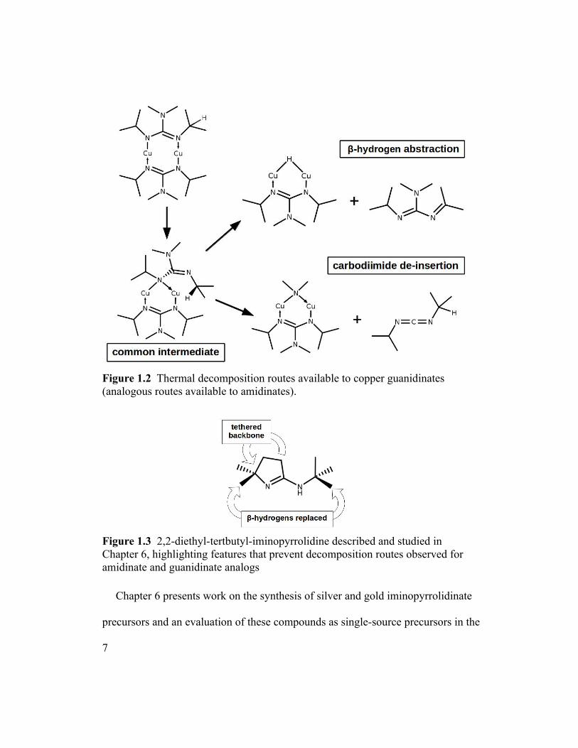
Figure 1.2 Thermal decomposition routes available to copper guanidinates (analogous routes available to amidinates).
Figure 1.3 2,2-diethyl-tertbutyl-iminopyrrolidine described and studied in Chapter 6, highlighting features that prevent decomposition routes observed for amidinate and guanidinate analogs
Chapter 6 presents work on the synthesis of silver and gold iminopyrrolidinate
precursors and an evaluation of these compounds as single-source precursors in the
7
thermal CVD deposition of metallic silver and gold thin films. The precursors' suitability
for use in gas-phase deposition was evaluated using thermogravimetric analysis (TGA ),
differential scanning calorimetry (DSC ), and NMR thermolysis studies. Depositions
were performed with and without nitrogen flow to study mass transport dynamics. Films
were analyzed by ellipsometry, XRD, SEM, EDS and XPS. To our knowledge, this is the
first time silver and gold iminopyrrolidinate species have been used for CVD.
Atomic Layer Deposition
Atomic layer deposition, while similar, is significantly different from CVD in terms of
how the film growth proceeds throughout the deposition. ALD is a gas-phase stepwise
thin film deposition method that results in highly conformal coverage of complex
surfaces.42 Where chemical vapour deposition is a continuous deposition process, ALD is
distinguished by the self-limiting nature of the molecular monolayer formed at each step.
Otherwise the requirements for precursor design are identical: high volatility, gas phase
stability and high reactivity at the substrate. The simplest ALD process sees the first
precursor, often but not necessarily a metal-organic species, entrained into a thermally-
defined deposition zone and over the target substrate. By design, this precursor saturates
the surface with chemisorbed species that render the surface inert, preventing further film
growth (this is the crux of the difference from a CVD process, which would continue
chemisorbing species for as long as they are entrained over the surface). A pulse of inert
gas followed by evacuation of the deposition chamber (a “purge” pulse) eliminates excess
8
precursor and the products of the chemisorption reaction. This prepares the system for the
next precursor which when entrained over the substrate reacts with the previous
monolayer to form another self-limiting monolayer. Another pulse/purge step follows and
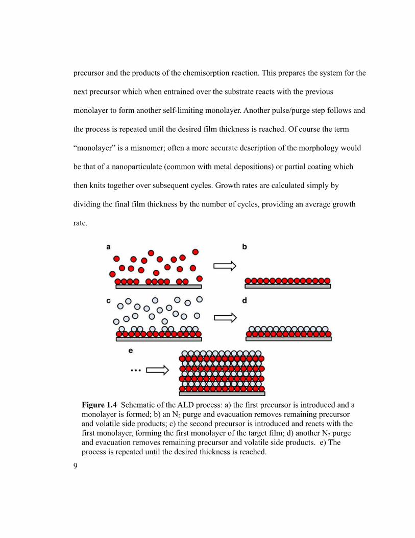
the process is repeated until the desired film thickness is reached. Of course the term
“monolayer” is a misnomer; often a more accurate description of the morphology would
be that of a nanoparticulate (common with metal depositions) or partial coating which
then knits together over subsequent cycles. Growth rates are calculated simply by
dividing the final film thickness by the number of cycles, providing an average growth
rate.
Figure 1.4 Schematic of the ALD process: a) the first precursor is introduced and a monolayer is formed; b) an N2 purge and evacuation removes remaining precursor and volatile side products; c) the second precursor is introduced and reacts with the first monolayer, forming the first monolayer of the target film; d) another N2 purge and evacuation removes remaining precursor and volatile side products. e) The process is repeated until the desired thickness is reached.
9
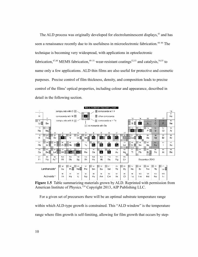
The ALD process was originally developed for electroluminescent displays,43 and has
seen a renaissance recently due to its usefulness in microelectronic fabrication.44–46 The
technique is becoming very widespread, with applications in optoelectronic
fabrication,47,48 MEMS fabrication,49–51 wear-resistant coatings52,53 and catalysis,54,55 to
name only a few applications. ALD thin films are also useful for protective and cosmetic
purposes. Precise control of film thickness, density, and composition leads to precise
control of the films’ optical properties, including colour and appearance, described in
detail in the following section.
Figure 1.5 Table summarizing materials grown by ALD. Reprinted with permission from American Institute of Physics.124 Copyright 2013, AIP Publishing LLC.
For a given set of precursors there will be an optimal substrate temperature range
within which ALD-type growth is constrained. This “ALD window” is the temperature
range where film growth is self-limiting, allowing for film growth that occurs by step-
10
wise reaction with a second precursor. The window is observed somewhere between the
volatilisation temperature and decomposition temperature of the precursor. At
temperatures below the window, film growth simply does not occur either because the
precursor is not volatile or it is unreactive with the substrate. At higher temperatures,
CVD-type growth that is not self-limiting is often observed. While film growth rates may
remain constant within the window, there are many reports in the literature of processes
were growth rates vary with temperature. Often the growth rates will increase with
increasing temperature, but the defining feature of ALD growth remains: step-wise and
self-limiting growth for a given temperature. Commonly, a precursor is limited to use in
CVD when the volatilisation temperature and decomposition temperature of the precursor
are not adequately separated.
1.2 ALD for Protective and Cosmetic Coatings
Protective Coatings
We investigated coatings offering two types of protection: protection from chemical
attack and protection from mechanical wear. The relatively small concentrations of
sulphides in the atmosphere is enough to tarnish otherwise untouched silver metal over
time, and metals that are subjected to more regular use such as tools or coins will at a
minimum be exposed to salt, sweat and oils in addition to airborne contaminants. A
protective coating must resist these chemical attacks as well as physical wear; a hard but
brittle coating that is highly resistant to chemical attack can nevertheless develop cracks,
11
admitting access to and corrosion of the underlying substrate. Resilience towards physical
attack requires a combination of toughness and flexibility. Cosmetic coatings present
their own, related set of challenges. If a specific colour of coating is desired (including
colourless), for example, the material must remain visually unchanged should
contaminants be absorbed. Additionally the coating must slow or prevent the
contaminants' diffusion towards contact with the substrate interface, to preclude any
chemical reactions that may alter the appearance of the substrate material or compromise
the adhesion of the film (such as the oxidation of metal substrates).
Conformal, complete coatings using a minimal thickness of material have generated
recent interest in ALD coatings as barriers to corrosion and mechanical wear. The
literature provides numerous examples of efforts to protect a wide variety of materials
including plastics for use in space,56 wood,57 and metals in diverse applications such as
silver museum pieces,58 ball bearings59 and brain implants.60 Most commonly the films
are deposited using well studied processes such as aluminum oxide or titanium oxide, but
other more exotic depositions have also been studied such as WS2, W/Al2O3 and
ZnO/ZrO2 laminates, and melt-compounded titanium dioxide
nanocomposites.59,61,52,62 Multilayer or laminate architectures have been found to impart
increased wear resistance to a coating.52 In part this is due to the frustration of crack
propagation: a single-material coating is more likely to crack all the way through to the
substrate, thus exposing the substrate to direct chemical attack. More generally, multiple
12
layers provide alternative pathways for the release of mechanical stress, reducing the
likelihood of the formation of a crack that leads directly to the surface.
Cosmetic Effects of Films: Interference Colours
The colours that result from thin film depositions are a complication that have not
garnered much attention in the literature thus far. For most protective coatings, such as
tools and ball bearings, the resulting colour is not a concern and the focus is on durability.
For cosmetic applications the resulting colour is of equal if not primary concern. The
colours exhibited by thin film coatings emerge from the phenomena of constructive and
destructive interference of light; these so-called “interference colours” are very well
understood. Consider a thin film of material on a substrate: a thin film that is necessarily
transparent to some degree, with an index of refraction different from that of the substrate
(Figure 2.1). Light may be reflected and/or refracted multiple times at each of the
interfaces encountered (air/film and film/substrate). The light observed by the eye will
therefore have constructively or destructively interfered with itself, as the process
ultimately results in reflections that can range from weak to strong depending on the
light's wavelength, the film thickness, the angle of incidence, and the physical constants
of the materials involved. A thin film illuminated with a beam of visible light of multiple
wavelength components will therefore produce a reflection that can be strong at some
wavelengths and weak at others, observed as a shift in the spectrum of the reflected beam
and therefore a shift in the perceived colour. For a given film/substrate pair, then, the
13
source of light will also contribute to the final result: sunlight will yield a different
perceived colour than fluorescent light, for example. Iridescence arises from the angular
dependence of phase change of the light, which is observed as the viewing angle deviates
from normal to the surface.
Figure 1.6 Model illustrating the origin of interference colours. A is an incident beam of light at a specific frequency. Due to partial reflection, it splits into beam C and B. Depending upon the thickness of the film (d) and the angle of incidence of A, the path length C+D may alter the phase of E with respect to B. Constructive or destructive interference may then occur, altering the wavelength of the outgoing light. The refractive indices of the materials are given by n1, n2 and n3.
Interference colours are strongest when the interfaces are at distances comparable to,
or smaller than, the light's coherence length (the distance over which the light wave can
be considered to be a single sinusoid) which for ordinary white light is on the order of a
few micrometers.63 These thicknesses are exactly where the precision and control of an
ALD process excels and furthermore multilayer structures are trivial, providing a high
degree of versatility and tunability for optical and cosmetic applications.
14
While interference colours for the films can be modelled to some extent, the pertinent
details of the actual physical system differ significantly from idealized models and thus
merit direct observation. For example the dispersion curve (the wavelength-dependent
index of refraction) for a bulk material may differ significantly from that of a thin film of
the same material due to the manner in which the film was grown. Annealing under
various gasses may further alter optical properties. Additionally, with respect to cosmetic
applications (which may be subject to a range of lighting and observation environments)
the perceived colour of the coated material may differ in subtle but significant ways from
the measured wavelengths. Furthermore, as the angle of incidence will alter the path
length of light through a given film, different viewing angles often result in different
perceived colours (iridescence). These subtleties can have a direct impact on the choices
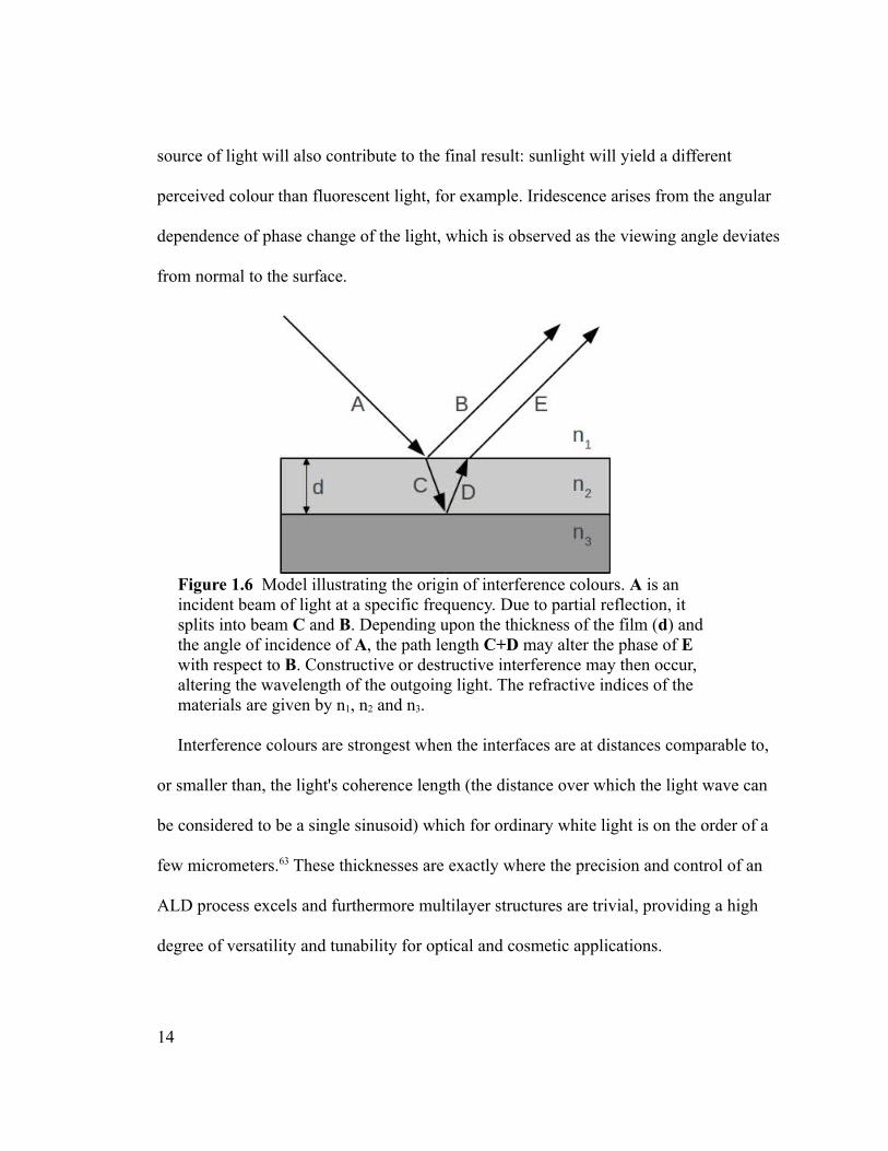
made for cosmetic coatings. The CIELab “colour space” formalism for describing
perceived colour is illustrated in (Figure 1.7). A difference of one unit along any of the
axes roughly corresponds to a difference in colour distinguishable by the human eye-
brain system.
15
Figure 1.7: Representation of the CIELab coordinate system for describing colour.
Goniocolourimetry is a technique used to measure the angular distribution of
perceived colour scattered from a surface (gonio = angular). Previous goniocolourimetric
analysis of thin films is extremely rare. Lamminpää et al. extracted the optical
parameters of SiO2 thin-film coatings based on reflectance and transmittance but do not
consider physiological colours as such.64 Diamanti et al. characterized the colours of
different titanium oxide films using spectrophotometry, but do not address angular
dependency.65 Beck et al. compared goniospectroscopy with spectroscopic ellipsometry
for the evaluation of the optical properties and colours of decorative coatings of Ti, TiN,
TiCN, TiCN and TiAlCN.66 Niyomsoan et al. investigated the colour variation in 0.5um
zirconium and titanium nitride decorative thin films with respect to the atomic ratio
between nitrogen and the metals with oxygen as a contaminant.67
16
Chapter 2 presents preliminary research into the colours produced by alumina and
titania deposited by ALD on copper alloys in small scale and large scale batches.
Protection from chemical attack and uniformity over large batches is also addressed.
Chapter 3 reports detailed goniocolourimetric analysis of alumina deposited by ALD on
silicon slides, comparing simulated spectra with observed spectra collected over a wide
range of observation angles. Deviations from the predicted observations are discussed.
1.3 Photovoltaic Devices
Photovoltaic devices exploit the photovoltaic effect to generate a useful electric
current from light. When light of the proper frequency impinges upon a material,
electrons in the valence band of the material can be excited to the conduction band. With
the proper architecture a device consisting of two materials can be created that then
separates these electrons from the resulting positively charged “holes” they leave behind,
guiding their flow in a manner that generates a useful electromotive force. The first such
practical device, achieving 6% efficiency, was created in 1954 at Bell Laboratories by
Daryl Chapin, Calvin Souther Fuller and Gerald Pearson, using a silicon p–n
junction.68 The basic architecture of this device is still in use today due to its simplicity
and effectiveness. A p-n junction is a physical interface between two materials, one that is
electron-rich (n-material) and one that is electron-poor (p-material). The composition of
these materials may be entirely different, or they may each consist primarily of the same
bulk material treated in such a way (e.g. doped with another element) as to make one
17
electron-rich and one electron-deficient. The materials are chosen such that the energy
gap (the band-gap) between the valence band of the n-material and the conduction band
of the p-material is on the order of the energy provided by the visible light spectrum.
When an electrically conductive connection is made between the two materials and light
of the appropriate frequency is absorbed, a direct current is generated as the resulting
electron-hole pair are attracted towards one another through the conductor.69 The
materials used and exact architecture vary considerably.
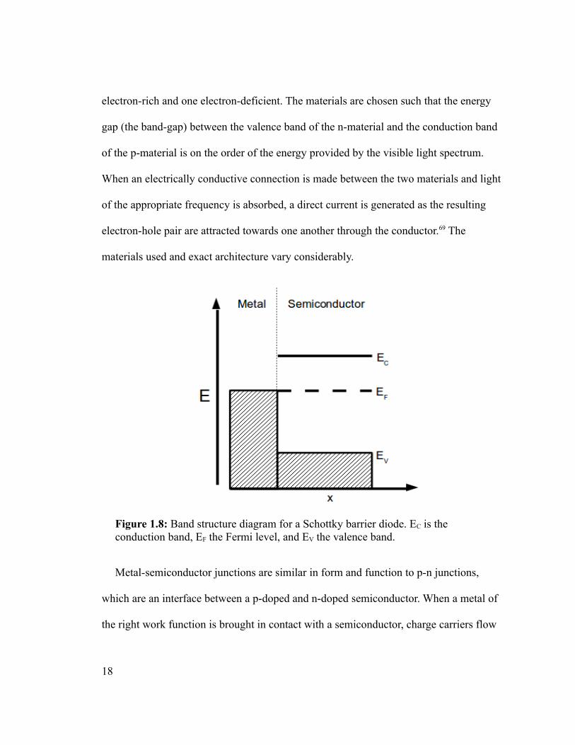
Figure 1.8: Band structure diagram for a Schottky barrier diode. EC is the conduction band, EF the Fermi level, and EV the valence band.
Metal-semiconductor junctions are similar in form and function to p-n junctions,
which are an interface between a p-doped and n-doped semiconductor. When a metal of
the right work function is brought in contact with a semiconductor, charge carriers flow
18
across the junction until a thermal equilibrium is established, much like a p-n junction.
This particular arrangement is called a Schottky-barrier diode (Figure 1.8). A Schottky
barrier is simply a potential energy barrier for electrons formed at a metal–semiconductor
junction. While these devices can act as solar cells, their photovoltaic conversion
efficiencies can be considerably increased by the presence of a thin interfacial insulating
layer (often an oxide) between the metal and the semiconductor. In a metal-SiO2-Si
structure for example, the insulating SiO2 layer must be extremely thin for optimal
performance: on the order of 10 Å.70 This architecture is called a metal-insulator-
semiconductor (MIS) structure. They received a great deal of attention in the 1970’s and
1980’s due to their relative economical advantage over the conventional p-n junction
solar cells. The reflectivity and poor light transmission properties of the top metal layer
limits the practical efficiencies of such cells, however.71–74 Nonetheless structures with
efficiencies of 10% - 15% have been demonstrated with theoretical efficiencies for flat Si
based cells reaching up to 20%.75,71 To eliminate the problem of highly reflective metal
layers, these have been replaced with transparent conductive oxides, yielding device
efficiencies of 11.5% for spray deposited indium-tin-oxide (ITO).74 Unfortunately, this
improvement also results in increased device cost as ITO remains a relatively expensive
material. This has motivated research into low-cost transparent conductor alternatives that
may be compatible with this architecture, such as poly(3,4-ethylenedioxythiophene)
poly(styrenesulfonate) (PEDOT:PSS).76
19
In Chapter 4 photovoltaic devices using the MIS architecture are assembled wherein
the “metal” is spin-coated PEDOT:PSS, the insulating layer is aluminum oxide deposited
by ALD, and the semiconductor is n-type silicon. The performance of flat and
nanostructured silicon are compared and the nanostructured silicon substrate is found to
generate a superior photovoltaic response.
20
Chapter 2 - Protective and Cosmetic Coatings for Coinage Metals and Their
Alloys
The work presented here is unpublished. It was performed in collaboration with the Royal Canadian Mint. Co-contributors to this work include Agnieszka Kurek, Adam Wells and Seán T. Barry.
2.1 Abstract
Stamped coins of brass and bronze were coated by ALD with alumina and titania.
These coatings were evaluated for use as protective and cosmetic coatings for circulation
and numismatic coinage. Initial alumina ALD experiments establishing proof of concept
on individual coins were performed, assessing feasibility and film continuity. These were
followed by scaled-up depositions on 2744 coins per batch where optimization of
deposition parameters for uniform coatings both on individual coins and across a batch
for alumina and titania films was performed. The effect of film thickness on colour was
examined and preliminary investigations of protective properties undertaken. The process
was optimized to minimize batch times, emulating an industrial setting. It was found that
high-quality, uniform coatings could be achieved with “multi-pulse” programs, yielding
coins indistinguishable by eye or touch from uncoated coins.
2.2 Introduction
Protecting bulk metals (mainly of Fe, Al, Cu, Zn, Mg and their alloys) from corrosion
has been a problem for centuries and remains a major ongoing concern in modern times.
A large number of coatings for corrosion inhibition have been developed where the 21
principle issue is oxidation and subsequent corrosion in air, with other considerations
dependent on the application, including mechanical wear, moisture, and specific chemical
concerns (salts, H2S, CO2, etc). Applications of significant concern in the literature
include corrosion inhibition in water cooling systems, in the oil and gas and electronics
industries, and generally inhibition of corrosion in industry due to acids.77
Recently, interesting work in this area includes polymer layers, silica-organic layers,
conversion layers, metallic layers and ceramic layers deposited by a wide variety of
methods to form self-healing anti-corrosion coatings.78 Inorganic-organic sol-gel methods
are widely used for thin ceramic coatings. Ceramic coatings are usually deposited on
metals to improve their performance in high temperature and/or abrasive environments
and have been shown to improve resistance against gas, solid, molten and condensed
phase oxidation and corrosion; decreasing wear; decreasing heat losses and/or reflecting
radiation in high temperature systems.79,80 Vapour-phase methods dominate the list of
techniques for protective coatings, but electrochemical plating is common as well. The
literature provides several examples of efforts to protect a wide variety of materials with
ALD coatings including plastics, wood, museum pieces and ball bearings.56–59 Most
commonly simple metal oxide films are used, but other more complex depositions using
laminates have generated interest as multilayer or laminate architectures have been found
to impart increased wear resistance to a coating.81
Research into protective coatings is primarily motivated by applications in industrial
settings or microelectronics and nanotechnology. With the notable exception of a patent
22
application from Beneq Oy for an ALD process used to coat silver with a variety of
transparent films (aluminum oxide, titanium oxide, chromium oxide, zirconium oxide,
indium oxide, and niobium oxide),82 very little work has been done in the area discussed
below, specifically: thin film protective coatings for legal tender that will see large scale,
public use (coins). The particular concerns of this type of application are similar but
distinct from industrial settings: the coatings must still protect against environmental
factors such as human sweat and oils, atmospheric components and significant
mechanical wear, but the substrates must continue to present a relatively unblemished and
uniform appearance that does not deviate from the established, accepted appearance of
the coins.
2.3 Results and Discussion
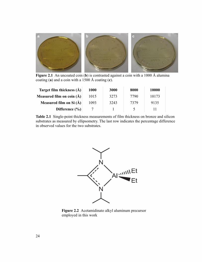
The feasibility of depositing alumina films on bronze Canadian dollar coins (minted
2009, 88% Cu, 12% Sn w/w, Figure 2.1) was initially assessed using a custom-built ALD
tool (Figure 2.8) and a previously reported83 acetamidinato alkyl aluminum compound
(Figure 2.2). A series of thicknesses were deposited on coins using these precursors,
ranging from 1000 Å to 10,000 Å. Silicon witness slides were included in each run for
characterization and comparison. Table 2.1 shows the values obtained for each by
ellipsometry.
23
Target film thickness (Å) 1000 3000 8000 10000
Measured film on coin (Å) 1015 3273 7790 10173
Measured film on Si (Å) 1093 3243 7379 9135
Difference (%) 7 1 5 11
Table 2.1 Single-point thickness measurements of film thickness on bronze and silicon substrates as measured by ellipsometry. The last row indicates the percentage difference in observed values for the two substrates.
Figure 2.2 Acetamidinato alkyl aluminum precursor employed in this work
24
Figure 2.1 An uncoated coin (b) is contrasted against a coin with a 1000 Å alumina coating (a) and a coin with a 1500 Å coating (c).
The coins were characterized by visual inspection (an important consideration for
legal tender), by SEM and using a electrodeposition test to evaluate film continuity.
Interference colours from the films altered the appearance of the coins, dramatically in
some cases. Figure 2.1 demonstrates the sensitivity of the eye to seemingly minor
differences in film thickness: 1000 Å and 1500 Å coatings produce clear changes in
perceived colour. Coin cleanliness prior to deposition also had a pronounced impact on
appearance. Any oils remaining on the coin, invisible prior to coating, are unmistakeably
highlighted by deposited films. This was mitigated by cleaning with soap and water,
sonication in distilled water, ethanol and then ether, and finally by treating the coins to a
5% H2 in N2 purge for 30 min at 200 °C in situ immediately prior to deposition. Substrate
cleanliness became a much more pressing issue once the project moved to batch
deposition experiments with implications for integration into bulk production, discussed
below. Thicker films resulted in a very interesting variety of colours, including
iridescence. Figure 2.3 shows a selection of results along with silicon witness slides for
comparison. As the interference colours produced are a function of the index of refraction
of both the film and the substrates, the colours produced on the coins and on the silicon
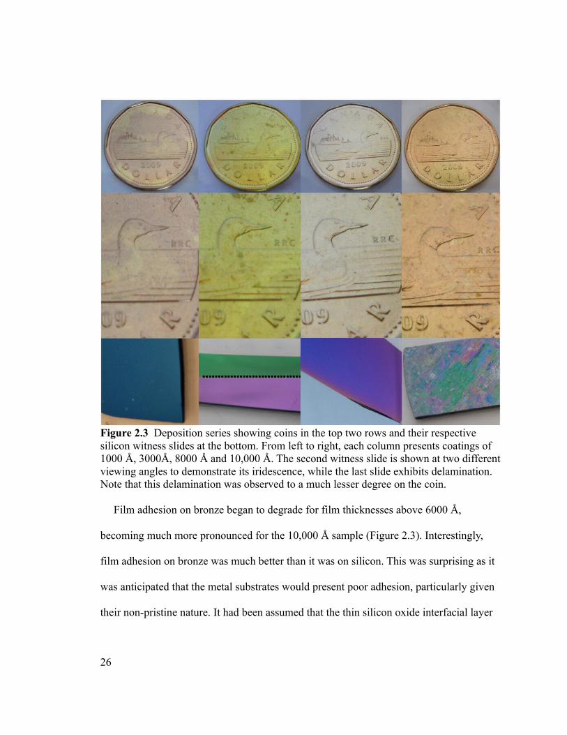
cannot be quantitatively compared. At a thickness of 3000 Å a pronounced iridescence
was observed on the coins: at low viewing angles the coin appeared mostly violet and at
high viewing angles (normal to the coin face) it appeared green (Figure 2.4).
25
Film adhesion on bronze began to degrade for film thicknesses above 6000 Å,
becoming much more pronounced for the 10,000 Å sample (Figure 2.3). Interestingly,
film adhesion on bronze was much better than it was on silicon. This was surprising as it
was anticipated that the metal substrates would present poor adhesion, particularly given
their non-pristine nature. It had been assumed that the thin silicon oxide interfacial layer
26
Figure 2.3 Deposition series showing coins in the top two rows and their respective silicon witness slides at the bottom. From left to right, each column presents coatings of 1000 Å, 3000Å, 8000 Å and 10,000 Å. The second witness slide is shown at two different viewing angles to demonstrate its iridescence, while the last slide exhibits delamination. Note that this delamination was observed to a much lesser degree on the coin.
which is unavoidable in alumina depositions on silicon would provide a strongly binding
intermediate layer between the silicon substrate and the Al2O3 film but the delamination
of the 10,000 Å film from the silicon was nearly complete, while the same film on the
coin showed only moderate delamination. It is well known that strain can originate from
growth on lattice-mismatched substrates and from post-growth cooling.84 The nature and
composition of the interface between the bronze substrate and alumina film is not known
and bears closer scrutiny.
Figure 2.4 Iridescence of 3000 Å film of Al2O3 on bronze.
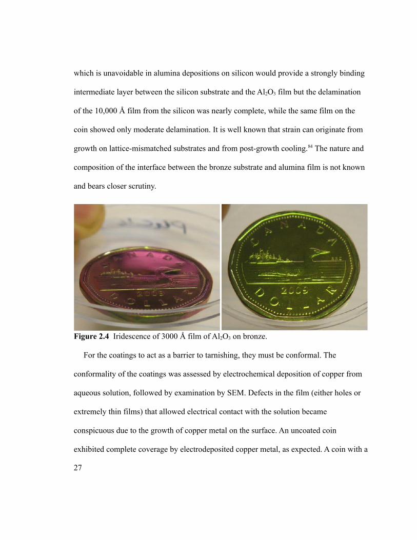
For the coatings to act as a barrier to tarnishing, they must be conformal. The
conformality of the coatings was assessed by electrochemical deposition of copper from
aqueous solution, followed by examination by SEM. Defects in the film (either holes or
extremely thin films) that allowed electrical contact with the solution became
conspicuous due to the growth of copper metal on the surface. An uncoated coin
exhibited complete coverage by electrodeposited copper metal, as expected. A coin with a
27
1000 Å coating subjected to the test was found to have only a few sites where copper
growth was observed by SEM, shown in Figure 2.5. This was an encouraging result given
the non-ideal nature of the substrates.
Figure 2.5 SEM image of a coin coated with 1000 Å Al2O3, after electrodeposition experiment. Copper metal (white) indicates a flaw in the film exposing the coin to the electrodeposition solution.
Batch Depositions
The results from these initial depositions on the custom-built reactor led to larger
scale, “bulk” depositions of alumina and titania using a Picosun SUNALE P-300B tool.
“Tokens” were used in place of legal tender and provided by the Mint; these had the same
28
dimensions, composition and processing as circulation coins used in previous testing with
the exception that they were stamped with a different image. A set of racks were
machined to hold the tokens parallel to system flow in a stacked configuration (Figure
2.9). A total of 2744 tokens could be loaded in this manner. The precursor chemistry was
changed to adapt to batch depositions as well; the well-known trimethyl
aluminum(TMA)/water precursor pair was used for aluminum oxide and a titanium
tetraisopropoxide/water pair was used for titanium oxide. Both of these new precursors
could be obtained commercially in large quantities at reasonable cost.
There was some concern that points of contact between the tokens and the racks could
lead to defects in the films due to obstruction of precursor flow. Indeed, prior to the
optimization of deposition parameters (specifically the thermal equilibration wait time
prior to deposition) some film irregularities were localized at points of contact. The
nonuniform growth observed near points of contact are attributed to a thermal gradient
rather than to any irregularities of precursor flow. There was in fact an altered growth rate
in these areas due to a thermal gradient as insufficient time had been allowed for the
entire thermal mass to equilibrate. The deposition chamber is heated by external sets of
resistively heated coils. As the deposition chamber was held under vacuum with no
convection currents to assist heat distribution, the majority of heat transfer was achieved
radiatively or by direct thermal contact of the internal components as the rack assembly
was directly affixed to the chamber ceiling. Those parts of the tokens in direct contact
with the racks were therefore warmer, leading to an altered film growth rate as compared
29
to the areas further away from the points of contact. The resulting film thickness gradient
was clearly observed by eye. The proper wait time for the system to reach thermal
equilibrium was established with an array of thermocouples affixed to a fully-loaded bulk
run, followed by verification with ALD deposition experiments. In this manner it was
determined that a thermal equilibration time of 6 hours for a process temperature of 250
°C was necessary for uniform film growth across all substrates. This process temperature
was chosen as it accommodated both the alumina and titania ALD processes, based on
literature values for the precursors employed.85,86 A study of the effectiveness of nitrogen
flow during the heating step to accelerate equilibration would be useful to reduce total
process time, but was beyond the scope of this work.
An issue of interest that then became obvious was initially attributed to non-uniform
coatings: a small number of individual tokens (approx. 0.6% of tokens) on an otherwise
successful deposition would present a colour markedly different from the rest. Further
testing with heating but without any precursor pulsing (essentially an anneal under
vacuum) produced similar results; a similar number of individual, randomly located
tokens would acquire an entirely uniform, slightly pink hue. This evidence and
discussions with the Mint revealed that the observed colour change was due to a variation
in the copper composition of the bronze coatings in these tokens, which can vary by as
much as ±5%. This is a known issue that is usually caught on the Mint production line by
visual inspection but our tokens were obtained prior to this step. The difference in colour
is subtle on the production line and was considerably enhanced by the thermal anneal
30
imposed by the ALD experiments. The colour change under anneal may be due to
preferential migration of the tin towards the surface but this was not verified or studied
further.
Tokens were provided by the Mint directly after stamping. This proved problematic
initially as a colourless, transparent oil (composition not divulged by the Mint) is used in
the stamping process that both aided the stamping process and protected coins and tokens
from tarnishing during subsequent transport. This oil interfered with the ALD process,
often causing a cloudiness in the coatings that was typically minimal but occasionally
noticeable on casual inspection. The solvent-based cleaning regimen used for individual
coins described earlier was not practical for batch depositions. To resolve the issue the
Mint began pre-treating the tokens with an anneal at 500 °C under hydrogen gas (exact
experimental details not divulged). To streamline this process for production, it was
proposed that this “hydrogen scrub” be performed in the ALD tool immediately prior to
deposition but this experiment is beyond the scope of the work described here.
Initial bulk ALD experiments employed standard, single pulse programs. These proved
inadequate for complete and uniform coatings. Replacing a single, long pulse with a
pulse program that used multiple pulses of the same precursor separated by short purges
resulted in uniform coverage. Long purges were still required between precursors. The
brief pauses to purge between each small pulse allowed the bubbler vapour pressure to
rise somewhat and so deliver a larger total precursor mass than a single pulse of
equivalent length could generate. Table 2.2 describes the pulse program timing in detail.
31
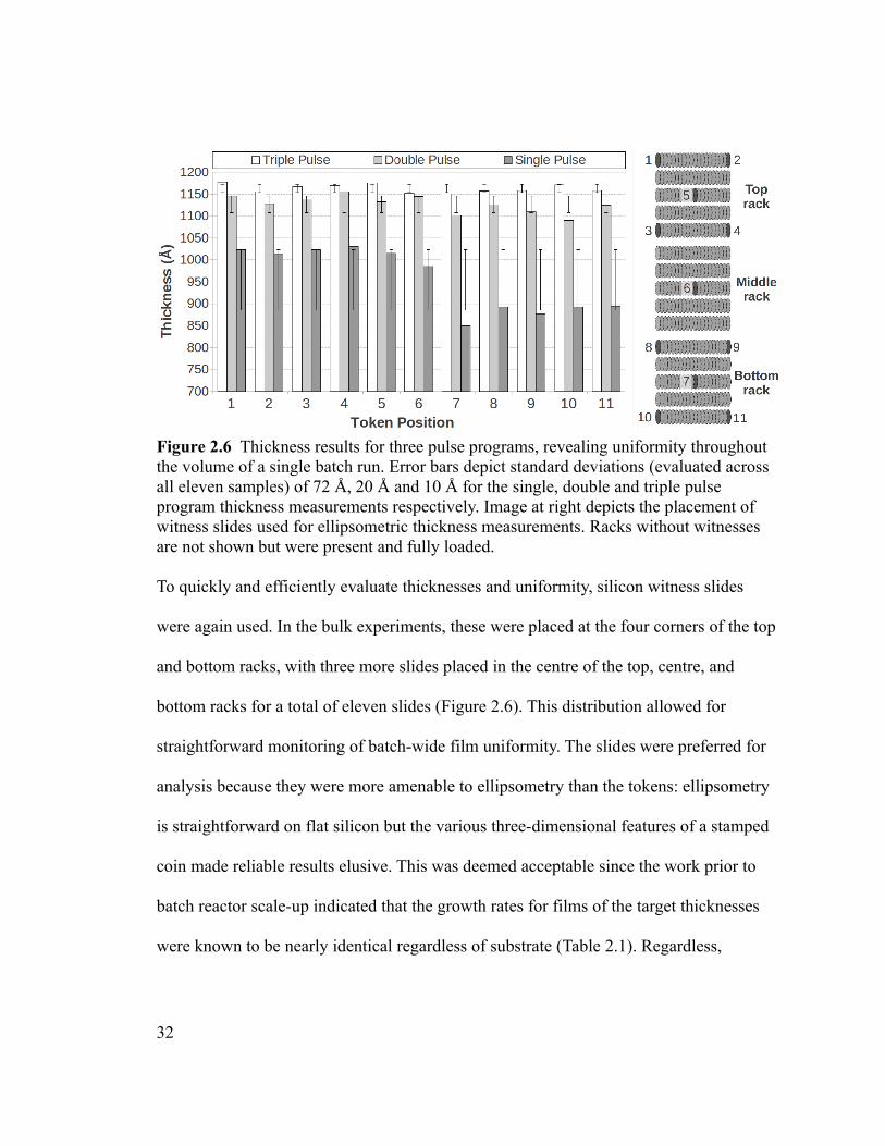
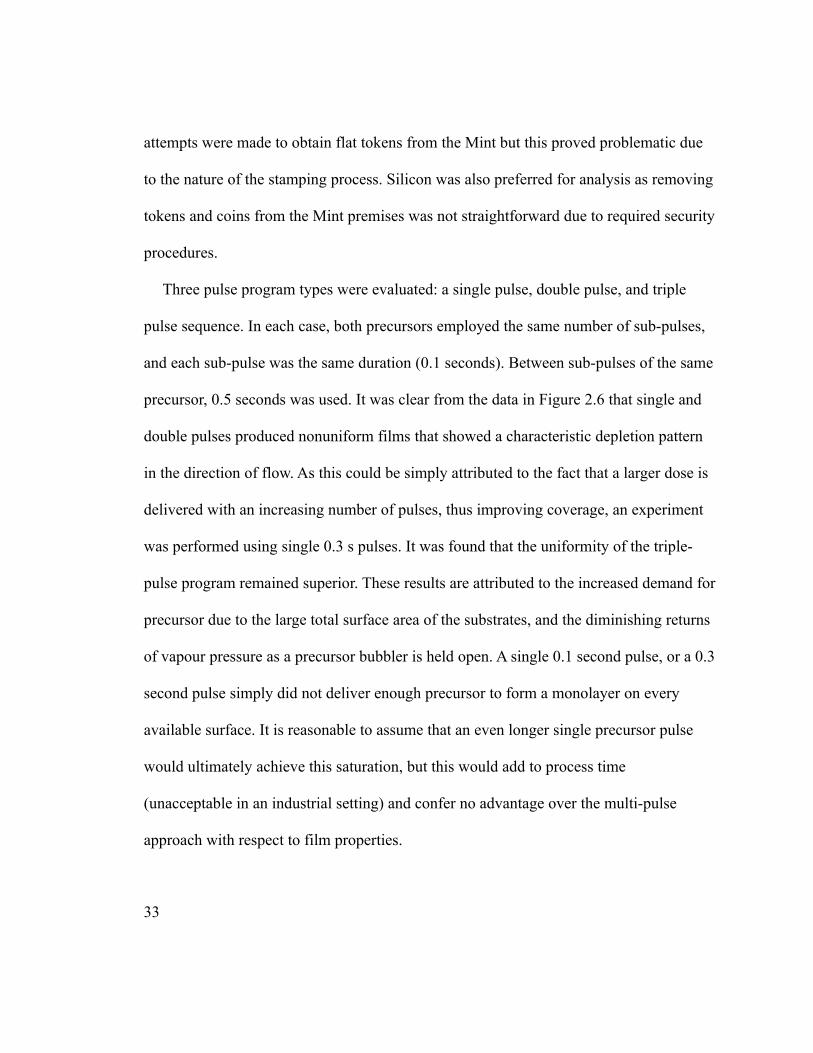
Figure 2.6 Thickness results for three pulse programs, revealing uniformity throughout the volume of a single batch run. Error bars depict standard deviations (evaluated across all eleven samples) of 72 Å, 20 Å and 10 Å for the single, double and triple pulse program thickness measurements respectively. Image at right depicts the placement of witness slides used for ellipsometric thickness measurements. Racks without witnesses are not shown but were present and fully loaded.
To quickly and efficiently evaluate thicknesses and uniformity, silicon witness slides
were again used. In the bulk experiments, these were placed at the four corners of the top
and bottom racks, with three more slides placed in the centre of the top, centre, and
bottom racks for a total of eleven slides (Figure 2.6). This distribution allowed for
straightforward monitoring of batch-wide film uniformity. The slides were preferred for
analysis because they were more amenable to ellipsometry than the tokens: ellipsometry
is straightforward on flat silicon but the various three-dimensional features of a stamped
coin made reliable results elusive. This was deemed acceptable since the work prior to
batch reactor scale-up indicated that the growth rates for films of the target thicknesses
were known to be nearly identical regardless of substrate (Table 2.1). Regardless,
32
attempts were made to obtain flat tokens from the Mint but this proved problematic due
to the nature of the stamping process. Silicon was also preferred for analysis as removing
tokens and coins from the Mint premises was not straightforward due to required security
procedures.
Three pulse program types were evaluated: a single pulse, double pulse, and triple
pulse sequence. In each case, both precursors employed the same number of sub-pulses,
and each sub-pulse was the same duration (0.1 seconds). Between sub-pulses of the same
precursor, 0.5 seconds was used. It was clear from the data in Figure 2.6 that single and
double pulses produced nonuniform films that showed a characteristic depletion pattern
in the direction of flow. As this could be simply attributed to the fact that a larger dose is
delivered with an increasing number of pulses, thus improving coverage, an experiment
was performed using single 0.3 s pulses. It was found that the uniformity of the triple-
pulse program remained superior. These results are attributed to the increased demand for
precursor due to the large total surface area of the substrates, and the diminishing returns
of vapour pressure as a precursor bubbler is held open. A single 0.1 second pulse, or a 0.3
second pulse simply did not deliver enough precursor to form a monolayer on every
available surface. It is reasonable to assume that an even longer single precursor pulse
would ultimately achieve this saturation, but this would add to process time
(unacceptable in an industrial setting) and confer no advantage over the multi-pulse
approach with respect to film properties.
33
For the triple pulse formulation, purge times between precursors were also optimized
to minimize total process time and maximize uniformity. A set of experiments evaluated
purge times of 5, 7.5 and 10 seconds for 1200-cycle depositions of alumina. Thickness
measurements yielded standard deviations of 39, 19 and 10 Å respectively clearly
indicating a purge of at least 10 seconds is required for maximum uniformity.
Additionally, shorter purge times resulted in thicker films, further indicating some CVD
growth taking place due to incomplete removal of co-reactants. Partly by trial and error
and partly through simulations with colourimetric simulation software (discussed in detail
in Chapter 3) it was found that alumina coatings on brass and bronze in a narrow range
around 1200 Å yielded tokens that were indistinguishable from uncoated tokens. TiO2
depositions were also tuned in this manner.
A small series of experiments depositing titania from titanium (IV) tetraisopropoxide
and water were also performed. In an initial experiment, coincident depositions of a
nominally 50 Å film of TiO2 on both a previously uncoated token and a token previously
coated with approximately 1200 Å Al2O3 were performed. XPS analysis was performed
to characterize the films. The results indicated poor growth on the bare tokens; titanium is
detected but the strength of the signal and the baseline of the data trace suggests a rough,
incomplete film. However, excellent growth of titania on alumina films was inferred as
no significant aluminum signal was detected by the instrument. This provides qualitative
evidence for the expected TiO2 film thickness of 50 Å, as this thickness exceeds the
penetration depth of the XPS x-rays thus rendering the alumina layer inaccessible to the
34
technique. Ellipsometric analysis of the film was attempted but the instrument was not
sensitive enough to deconvolute the two coatings. With this encouraging preliminary data
a series of laminate structures were generated, always using alumina as a base layer. The
characterization of these is beyond the scope of the present work.
Figure 2.7 XPS spectra of a bare token exposed to a TiO2 ALD process (a) and a token with a 1200 Å Al2O3 coating exposed to the same TiO2 ALD process (b). The shape of the baseline in a suggests a rough surface. Note that no aluminum oxide process was applied to sample a; the Al signal is marked there for comparison with b.
2.4 Experimental
Small Scale Depositions
Canadian Dollar Coins (minted 2009) were coated in these experiments, delivered in
person by a Mint representative from the production line. They were 26.5 mm in
diameter, 1.95 mm thick, composed of a nickel core and plated with bronze (approx. 88%
Cu, 12% Sn w/w). Prior to deposition they were hand washed with soap and water, then
35
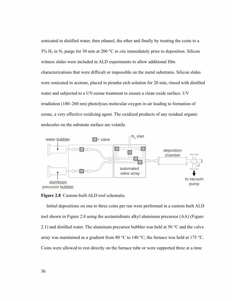
sonicated in distilled water, then ethanol, the ether and finally by treating the coins to a
5% H2 in N2 purge for 30 min at 200 °C in situ immediately prior to deposition. Silicon
witness slides were included in ALD experiments to allow additional film
characterizations that were difficult or impossible on the metal substrates. Silicon slides
were sonicated in acetone, placed in piranha etch solution for 20 min, rinsed with distilled
water and subjected to a UV-ozone treatment to ensure a clean oxide surface. UV
irradiation (180–260 nm) photolyses molecular oxygen in air leading to formation of
ozone, a very effective oxidizing agent. The oxidized products of any residual organic
molecules on the substrate surface are volatile.
Figure 2.8 Custom-built ALD tool schematic.
Initial depositions on one to three coins per run were performed in a custom built ALD
tool shown in Figure 2.8 using the acetamidinato alkyl aluminum precursor (AA) (Figure
2.1) and distilled water. The aluminum precursor bubbler was held at 50 °C and the valve
array was maintained as a gradient from 80 °C to 140 °C; the furnace was held at 175 °C.
Coins were allowed to rest directly on the furnace tube or were supported three at a time
36
by a custom built coin holder that had been passivated with at least 100 Å alumina prior
to use. The pulse program employed was as follows: (1) 5.0 s purge with N2, evacuate for
10.0 s; (2) 5.0 s fill aluminum precursor bubbler with N2 carrier gas; (3) 5.0 s entrain
aluminum precursor with carrier gas; (4) 5.0 s purge with N2, evacuate for 10.0 s; (5) 5.0
s fill H2O bubbler with N2 carrier gas; and (6) 5.0 s entrain H2O with carrier gas.
All small scale depositions began with 30 min of substrate passivation under 1.0 Torr
of 5% H2 in N2 at process temperature to ensure a hydrogen-terminated metal surface.
Batch Depositions
Two types of so-called “tokens” were used in batch depositions as samples
representative of Canadian Dollar Coins so as to avoid consuming large amounts of legal
tender; brass and bronze-coated versions of the coins described above with roughly the
same dimensions and composition. Brass is an alloy of copper and zinc (nominal
composition not divulged). These tokens are commonly used at the Mint for process
testing purposes. Initial bulk ALD experiments were conducted on “as-received” tokens
directly from the Mint, which were delivered in vacuum-sealed packaging.
Batch depositions were performed at a process temperature of 250 °C on a Picosun
SUNALE P-300B tool using TMA, titanium(IV) isopropoxide, and water. The pulse
programs used for alumina and titania coatings are described in Table 2.2. It was found
that longer pulses were necessary for each precursor for the titania coatings. Longer
37
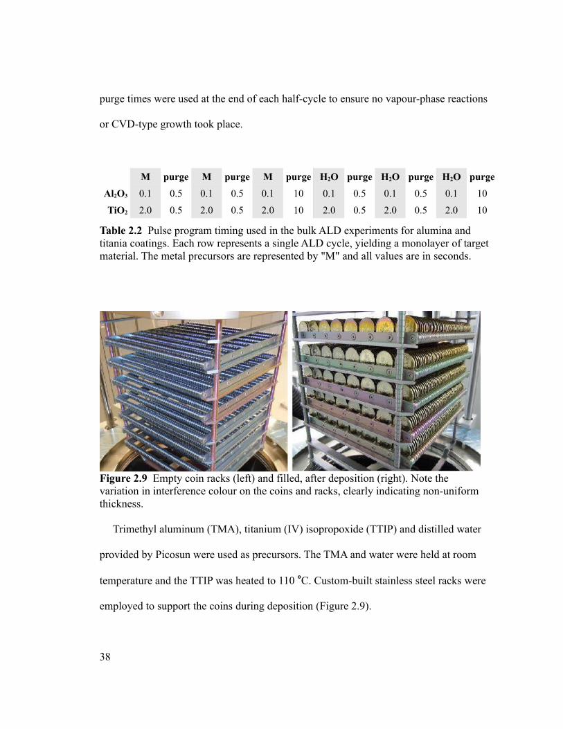
purge times were used at the end of each half-cycle to ensure no vapour-phase reactions
or CVD-type growth took place.
M purge M purge M purge H2O purge H2O purge H2O purge
Al2O3 0.1 0.5 0.1 0.5 0.1 10 0.1 0.5 0.1 0.5 0.1 10
TiO2 2.0 0.5 2.0 0.5 2.0 10 2.0 0.5 2.0 0.5 2.0 10
Table 2.2 Pulse program timing used in the bulk ALD experiments for alumina and titania coatings. Each row represents a single ALD cycle, yielding a monolayer of target material. The metal precursors are represented by "M" and all values are in seconds.
Figure 2.9 Empty coin racks (left) and filled, after deposition (right). Note the variation in interference colour on the coins and racks, clearly indicating non-uniform thickness.
Trimethyl aluminum (TMA), titanium (IV) isopropoxide (TTIP) and distilled water
provided by Picosun were used as precursors. The TMA and water were held at room
temperature and the TTIP was heated to 110 °C. Custom-built stainless steel racks were
employed to support the coins during deposition (Figure 2.9).
38
Electrodeposition Testing for Film Continuity
An 80 mL solution of 1.0 M H2SO4 and 0.4 M CuSO4 was prepared from 4.4 mL
concentrated H2SO4 and 8 g of solid CuSO4 dissolved in distilled water. A small section
of a coin coated by ALD was abraded with sandpaper to expose a metallic area for
electrical contact. The exposed area of the coin was affixed to an electrode and the coated
portion of the coin was suspended in the solution. Another electrode was affixed to a
copper gasket and likewise suspended in the solution. The electrodes were connected to a
power supply, and a voltage of 0.5 V and a current of 0.08 A was supplied for 4 minutes.
An identical arrangement was employed to evaluate uncoated coins for comparison.
Characterization
Al2O3 film thicknesses were determined by ellipsometry (Plasmos, HeNe laser at λ =
632 nm, nSi = 3.882, nalumina = 1.76, nCu = 2.43). Scanning electron microscopy was
performed using a Tescan Vega-II XMU. X-ray Photoelectron Spectroscopy was
performed using a Kratos Axis Ultra DLD instrument, with monochromated aluminum
Kα x-rays at 140W. A charge neutralizing electron floodgun was employed for insulating
samples.
39
2.5 Conclusions
Aluminum oxide was deposited on individual bronze circulation coins with a
previously reported process using an acetamidinato alkyl aluminum precursor and water.
Ellipsometric characterization of the coins and silicon witness slides revealed that for
deposited thicknesses on the order of 1000 – 10,000 Å, growth rates were independent of
substrate. With microscopy and visual inspection it was found that the films adhered
more strongly to the metal substrates than to the silicon at film thicknesses of 6000 Å and
above. Aluminum oxide, titanium oxide, and laminate combinations of these materials
were deposited on bulk quantities of brass and bronze tokens. It was determined that a
pulse program with three subsets of precursor/purge pulses for each precursor was
required for completely uniform coatings on all 2,744 tokens at 250 °C.
As uniformity of look and feel is important for legal tender, special attention was paid
to the interference colours produced by the deposited films. A film of approximately 1200
Å was found to yield coins nearly indistinguishable from uncoated coins. While not
necessarily desirable for introduction into circulation, other thicknesses produced an
array of colours including iridescence that may prove useful for numismatic, limited
edition coins. These optical properties also merit investigation as anti-counterfeiting
measures. A study of the nature and composition of the interface layer between metal
substrates and alumina film would help to understand both protective and cosmetic
issues.
40
Chapter 3 - Goniocolorimetric Study of Aluminum Oxide Films Deposited
by Atomic Layer Deposition
Modified from original manuscript, published as: Gordon, P. G.; Baribeau, R.1; Barry, S. T.2; “Goniocolorimetric Study of Aluminum Oxide Films Deposited by Atomic Layer Deposition”, Thin Solid Films, 2012, 520, 2943. 1 Institute for National Measurement Standards, National Research Council Canada, 1200 Montreal Road, Ottawa, ON, K1A 0R6, Canada2 Department of Chemistry, Carleton University, Ottawa, ON, K1S 5B6, Canada
3.1 Abstract
The interference colours resulting from thin films of Al2O3 deposited by atomic layer
deposition (ALD) on silicon have been rigorously analyzed using a newly developed
robotic gonioreflectometer. A series of eleven increasingly thick films were deposited, up
to 1613 Å, and their reflectivity values obtained for the visible spectrum. A comparison
of these values with the predictions of computer simulations employing Fresnel equations
has revealed that while there was generally good agreement between predicted and
measured spectra, there are some spectral regions that exhibit large deviations from
predicted reflectivities, in particular at near-normal measurement angles and shorter
wavelengths. The effect of these discrepancies on colour appearance was investigated in
the CIE L*a*b* colour space for the daylight illuminant D65. Large iridescence is both
predicted and measured for most film thicknesses. Chroma and hue differences as large
as 20 CIELAB units between the predicted and the measured colour centers were
obtained. Simulation also predicts larger iridescence than what is actually measured. A
41
likely cause for the observed discrepancies is that the dielectric constants of the ALD
films deviate from the literature values for the bulk material.
3.2 Introduction
Herein we describe a rigorous analysis of the interference colours that arise from thin
aluminum oxide films deposited on silicon substrates. The goniocolourimetric analysis in
this work makes use of a gonioreflectometer recently developed to measure the angular
distribution of the light reflected by opaque materials.87 The regular spectral reflectance
of the sample is measured precisely over the visible range from 380 nm to 780 nm and
for incidence angles varying from near normal to near grazing. International
Commission on Illumination (CIE) lightness, chroma and hue values are calculated for a
standard illuminant representative of daylight, and are plotted in CIELAB colour space to
demonstrate the variation of colour with thickness and angle, and to compare with
theoretical predictions. Simonot et al. have demonstrated a method for adapting the
CIELAB space to goniocolourimetric measurements of glossy and iridescent objects.88
The aluminum precursor employed for ALD film growth was [MeC(NiPr)2]AlEt2
(Figure 3.1). This precursor and the deposition process employed in this work are
described elsewhere.83
42
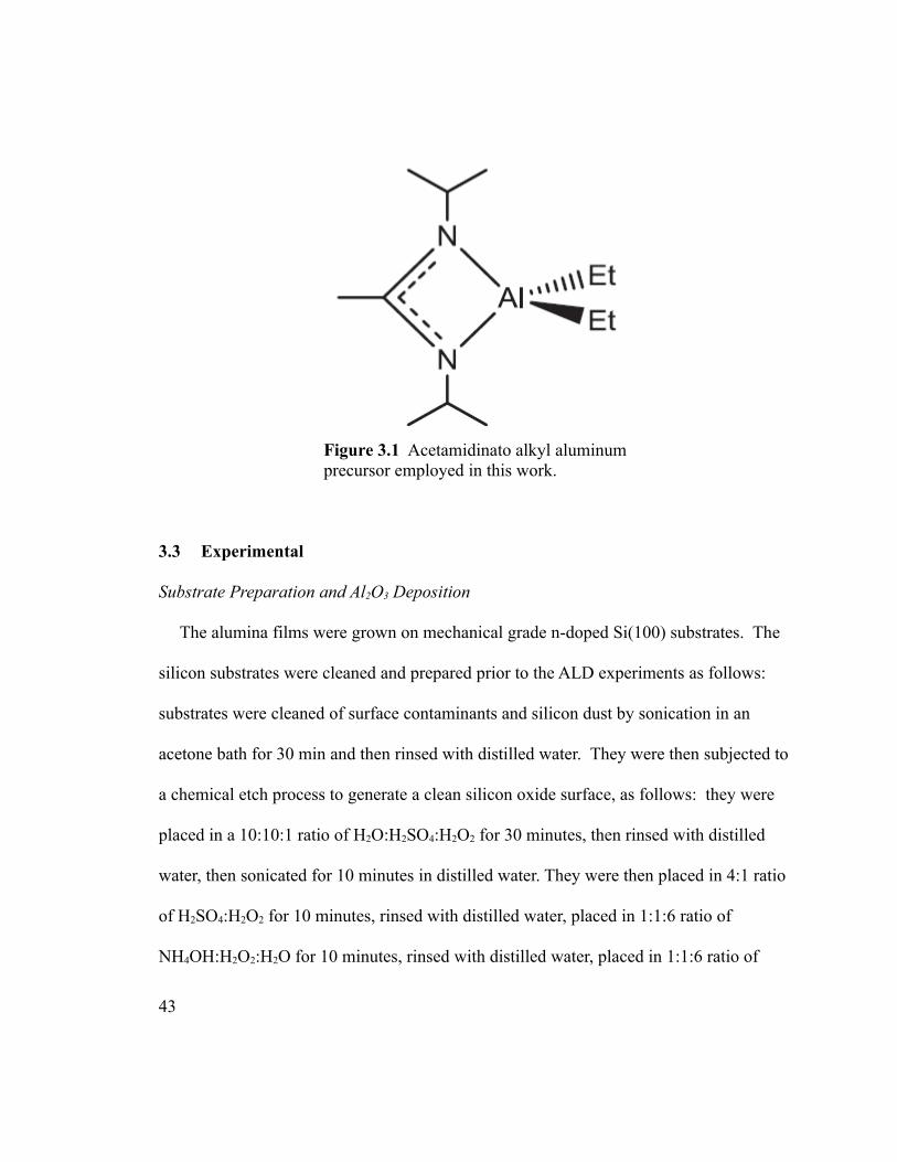
Figure 3.1 Acetamidinato alkyl aluminum precursor employed in this work.
3.3 Experimental
Substrate Preparation and Al2O3 Deposition
The alumina films were grown on mechanical grade n-doped Si(100) substrates. The
silicon substrates were cleaned and prepared prior to the ALD experiments as follows:
substrates were cleaned of surface contaminants and silicon dust by sonication in an
acetone bath for 30 min and then rinsed with distilled water. They were then subjected to
a chemical etch process to generate a clean silicon oxide surface, as follows: they were
placed in a 10:10:1 ratio of H2O:H2SO4:H2O2 for 30 minutes, then rinsed with distilled
water, then sonicated for 10 minutes in distilled water. They were then placed in 4:1 ratio
of H2SO4:H2O2 for 10 minutes, rinsed with distilled water, placed in 1:1:6 ratio of
NH4OH:H2O2:H2O for 10 minutes, rinsed with distilled water, placed in 1:1:6 ratio of
43
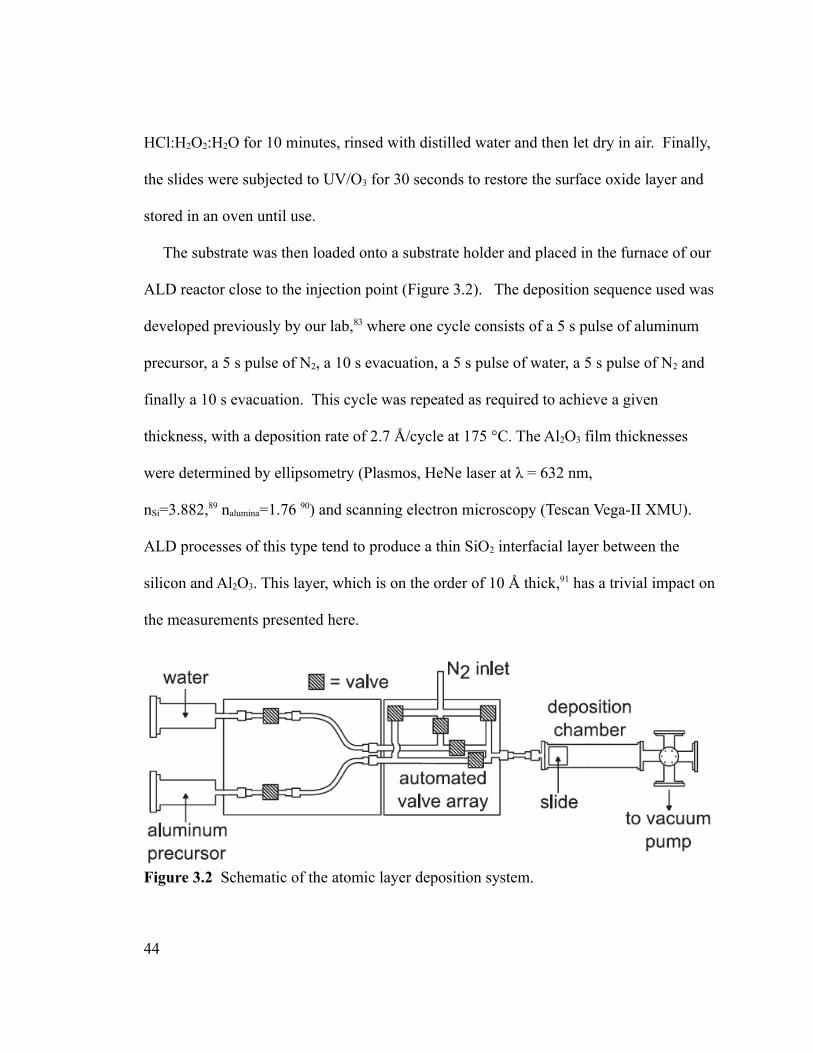
HCl:H2O2:H2O for 10 minutes, rinsed with distilled water and then let dry in air. Finally,
the slides were subjected to UV/O3 for 30 seconds to restore the surface oxide layer and
stored in an oven until use.
The substrate was then loaded onto a substrate holder and placed in the furnace of our
ALD reactor close to the injection point (Figure 3.2). The deposition sequence used was
developed previously by our lab,83 where one cycle consists of a 5 s pulse of aluminum
precursor, a 5 s pulse of N2, a 10 s evacuation, a 5 s pulse of water, a 5 s pulse of N2 and
finally a 10 s evacuation. This cycle was repeated as required to achieve a given
thickness, with a deposition rate of 2.7 Å/cycle at 175 °C. The Al2O3 film thicknesses
were determined by ellipsometry (Plasmos, HeNe laser at λ = 632 nm,
nSi=3.882,89 nalumina=1.76 90) and scanning electron microscopy (Tescan Vega-II XMU).
ALD processes of this type tend to produce a thin SiO2 interfacial layer between the
silicon and Al2O3. This layer, which is on the order of 10 Å thick,91 has a trivial impact on
the measurements presented here.
Figure 3.2 Schematic of the atomic layer deposition system.
44
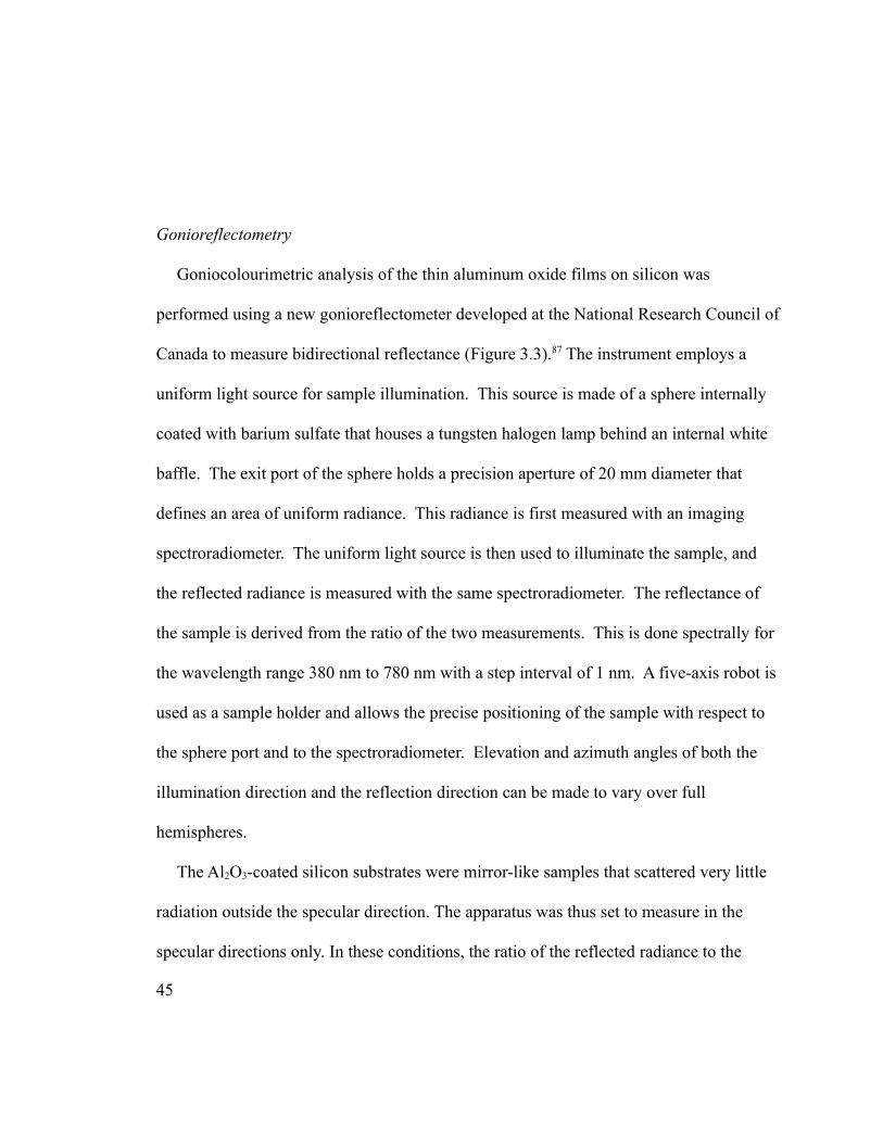
Gonioreflectometry
Goniocolourimetric analysis of the thin aluminum oxide films on silicon was
performed using a new gonioreflectometer developed at the National Research Council of
Canada to measure bidirectional reflectance (Figure 3.3).87 The instrument employs a
uniform light source for sample illumination. This source is made of a sphere internally
coated with barium sulfate that houses a tungsten halogen lamp behind an internal white
baffle. The exit port of the sphere holds a precision aperture of 20 mm diameter that
defines an area of uniform radiance. This radiance is first measured with an imaging
spectroradiometer. The uniform light source is then used to illuminate the sample, and
the reflected radiance is measured with the same spectroradiometer. The reflectance of
the sample is derived from the ratio of the two measurements. This is done spectrally for
the wavelength range 380 nm to 780 nm with a step interval of 1 nm. A five-axis robot is
used as a sample holder and allows the precise positioning of the sample with respect to
the sphere port and to the spectroradiometer. Elevation and azimuth angles of both the
illumination direction and the reflection direction can be made to vary over full
hemispheres.
The Al2O3-coated silicon substrates were mirror-like samples that scattered very little
radiation outside the specular direction. The apparatus was thus set to measure in the
specular directions only. In these conditions, the ratio of the reflected radiance to the
45
incident radiance corresponds to regular reflectance, a perfect mirror having a regular
reflectance of 1.
The samples were measured for incidence angles (equal to the reflection angles)
ranging from 10° to 70° in steps of 5°; 10° corresponds to the minimum angle allowed
before the sphere source occludes the detection path. For the measurement, the
spectroradiometer stays focused on the mirror image of the uniform light source port to
measure the central (3.5 mm diameter) portion. The sample itself acted as a mirror of
finite size that can clip some of the reflected rays at large incidence angles. The angle of
70° corresponds to maximum incidence angle allowed for the samples (approximately 3.3
cm square) before this clipping occurs. The angular resolution is 1.2° and corresponds to
the spectroradiometer’s field angle (0.2°) plus the angular aperture of its imaging lens
(1°).
46
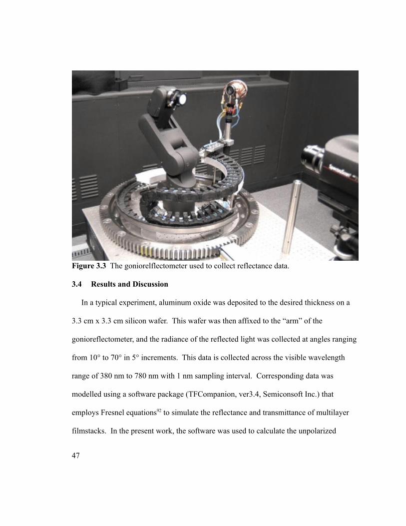
Figure 3.3 The goniorelflectometer used to collect reflectance data.
3.4 Results and Discussion
In a typical experiment, aluminum oxide was deposited to the desired thickness on a
3.3 cm x 3.3 cm silicon wafer. This wafer was then affixed to the “arm” of the
gonioreflectometer, and the radiance of the reflected light was collected at angles ranging
from 10° to 70° in 5° increments. This data is collected across the visible wavelength
range of 380 nm to 780 nm with 1 nm sampling interval. Corresponding data was
modelled using a software package (TFCompanion, ver3.4, Semiconsoft Inc.) that
employs Fresnel equations92 to simulate the reflectance and transmittance of multilayer
filmstacks. In the present work, the software was used to calculate the unpolarized
47
reflectance, which is an arithmetic mean of the reflectance of the p- and s-polarized light,
over the same angles and wavelengths measured by the gonioreflectometer. In general,
there was good agreement between the observed response to incident light and the
theoretical prediction (Figure 3.4). Figure 3.4(a) represents the observed reflectance
(expressed as a percent) of light topographically over a data plane of wavelength versus
film thickness, while Figure 3.4(b) represents the predicted values of these same data. It
should be noted that the entire data space has the variables of film thickness, wavelength
of reflected light, viewing angle, and percent reflectance. Thus, the data presented in the
figures must always be a subset of the data space.
48
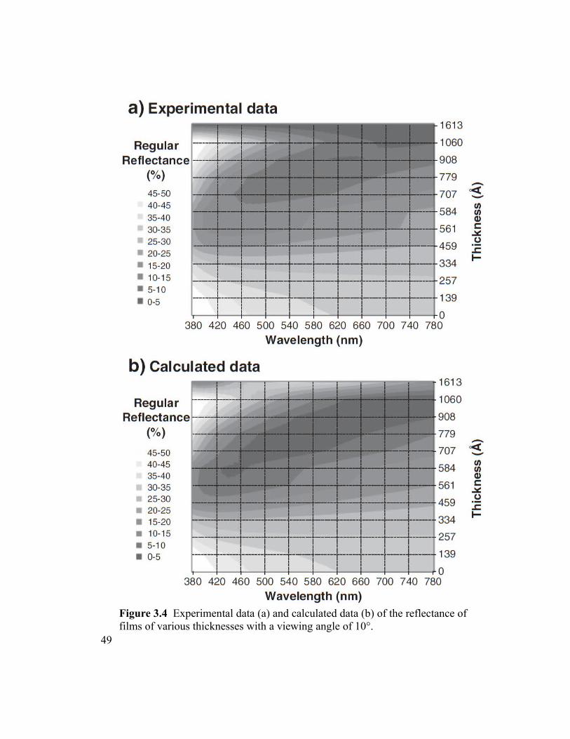
Figure 3.4 Experimental data (a) and calculated data (b) of the reflectance of films of various thicknesses with a viewing angle of 10°.
49
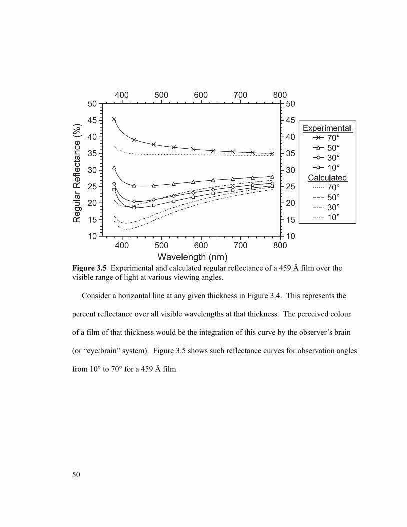
Consider a horizontal line at any given thickness in Figure 3.4. This represents the
percent reflectance over all visible wavelengths at that thickness. The perceived colour
of a film of that thickness would be the integration of this curve by the observer’s brain
(or “eye/brain” system). Figure 3.5 shows such reflectance curves for observation angles
from 10° to 70° for a 459 Å film.
50
Figure 3.5 Experimental and calculated regular reflectance of a 459 Å film over the visible range of light at various viewing angles.
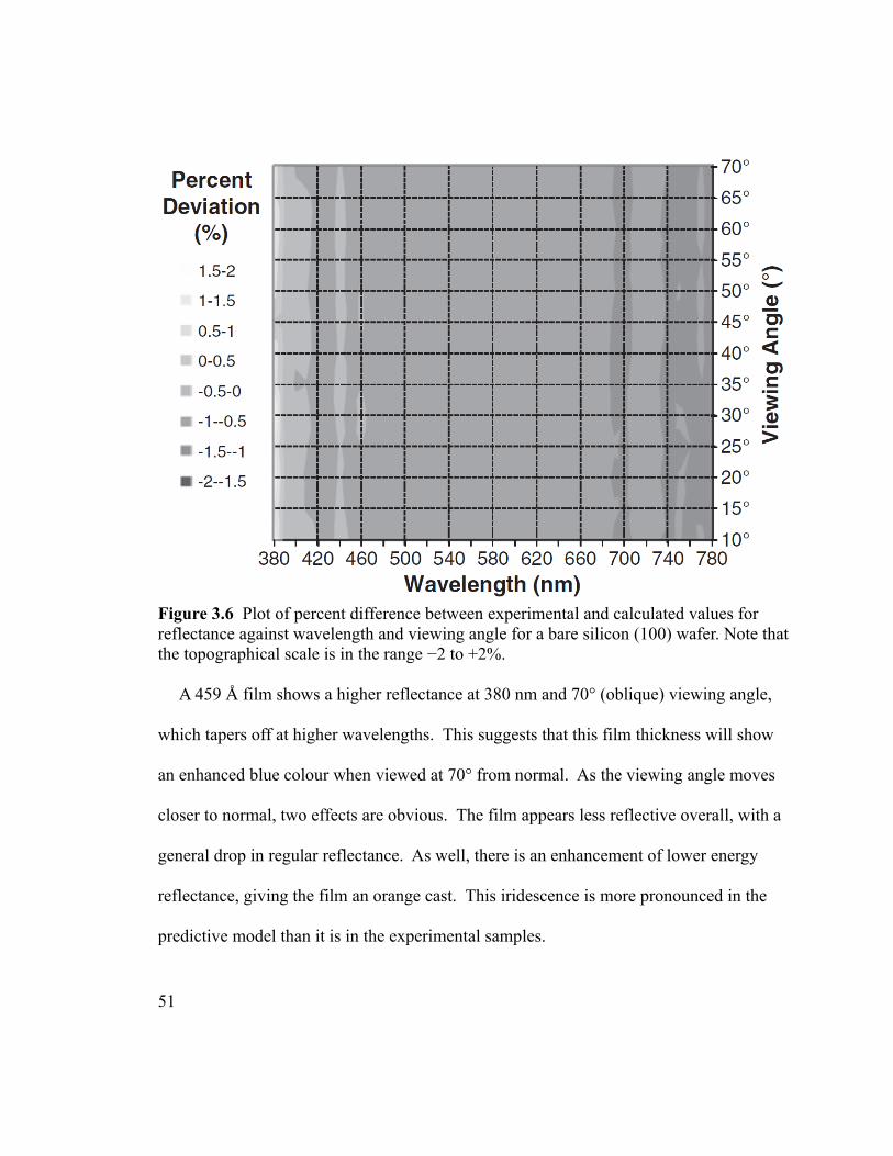
Figure 3.6 Plot of percent difference between experimental and calculated values for reflectance against wavelength and viewing angle for a bare silicon (100) wafer. Note that the topographical scale is in the range −2 to +2%.
A 459 Å film shows a higher reflectance at 380 nm and 70° (oblique) viewing angle,
which tapers off at higher wavelengths. This suggests that this film thickness will show
an enhanced blue colour when viewed at 70° from normal. As the viewing angle moves
closer to normal, two effects are obvious. The film appears less reflective overall, with a
general drop in regular reflectance. As well, there is an enhancement of lower energy
reflectance, giving the film an orange cast. This iridescence is more pronounced in the
predictive model than it is in the experimental samples.
51
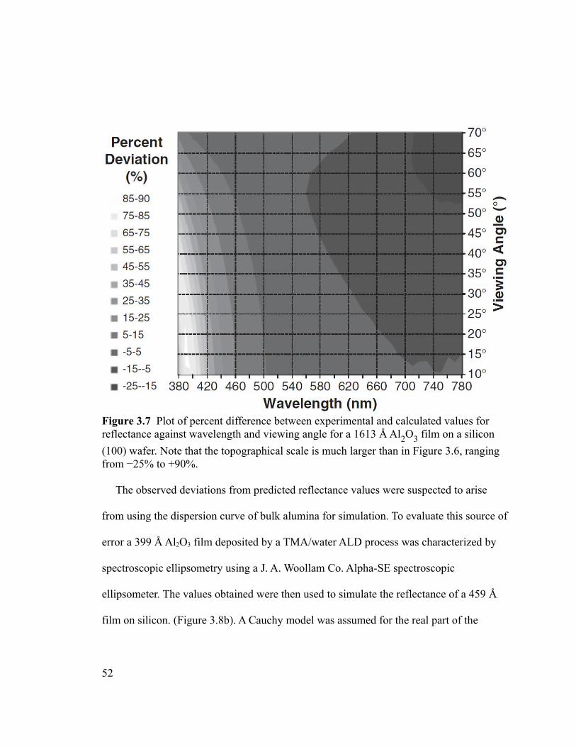
Figure 3.7 Plot of percent difference between experimental and calculated values for reflectance against wavelength and viewing angle for a 1613 Å Al2O3 film on a silicon
(100) wafer. Note that the topographical scale is much larger than in Figure 3.6, ranging from −25% to +90%.
The observed deviations from predicted reflectance values were suspected to arise
from using the dispersion curve of bulk alumina for simulation. To evaluate this source of
error a 399 Å Al2O3 film deposited by a TMA/water ALD process was characterized by
spectroscopic ellipsometry using a J. A. Woollam Co. Alpha-SE spectroscopic
ellipsometer. The values obtained were then used to simulate the reflectance of a 459 Å
film on silicon. (Figure 3.8b). A Cauchy model was assumed for the real part of the
52
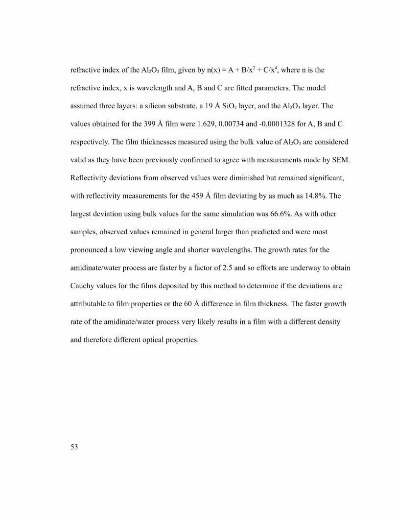
refractive index of the Al2O3 film, given by n(x) = A + B/x2 + C/x4, where n is the
refractive index, x is wavelength and A, B and C are fitted parameters. The model
assumed three layers: a silicon substrate, a 19 Å SiO2 layer, and the Al2O3 layer. The
values obtained for the 399 Å film were 1.629, 0.00734 and -0.0001328 for A, B and C
respectively. The film thicknesses measured using the bulk value of Al2O3 are considered
valid as they have been previously confirmed to agree with measurements made by SEM.
Reflectivity deviations from observed values were diminished but remained significant,
with reflectivity measurements for the 459 Å film deviating by as much as 14.8%. The
largest deviation using bulk values for the same simulation was 66.6%. As with other
samples, observed values remained in general larger than predicted and were most
pronounced a low viewing angle and shorter wavelengths. The growth rates for the
amidinate/water process are faster by a factor of 2.5 and so efforts are underway to obtain
Cauchy values for the films deposited by this method to determine if the deviations are
attributable to film properties or the 60 Å difference in film thickness. The faster growth
rate of the amidinate/water process very likely results in a film with a different density
and therefore different optical properties.
53
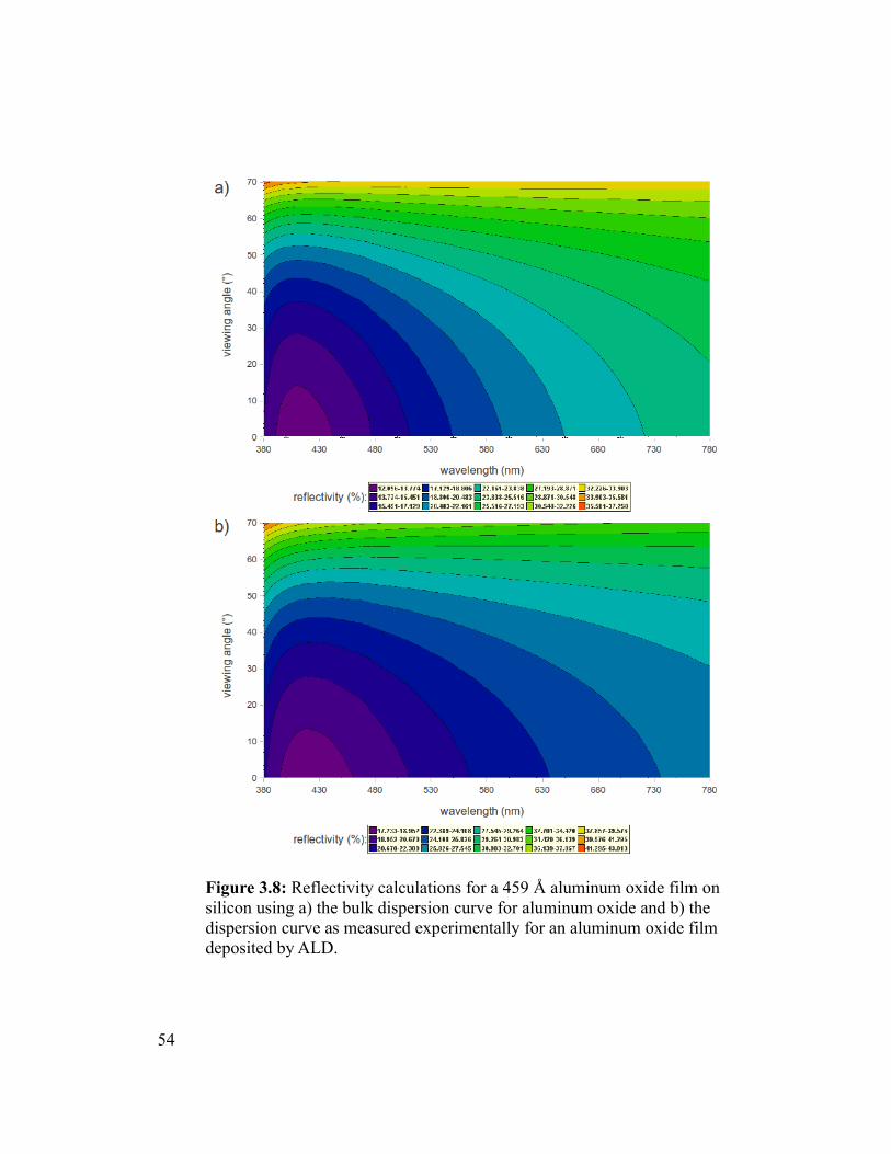
54
Figure 3.8: Reflectivity calculations for a 459 Å aluminum oxide film on silicon using a) the bulk dispersion curve for aluminum oxide and b) the dispersion curve as measured experimentally for an aluminum oxide film deposited by ALD.
Figure 3.9 a*b* CIELAB (CIE D65) plots of (a) observed and (b) calculated data for selected film thicknesses over a range of viewing angles. Coloured axes are approximate representations of the CIELAB space to help guide the eye.
A comparison of the calculated versus experimental data showed an interesting trend.
When predicting the difference in reflectivity of a bare silicon substrate, the model
showed only ±2% error (measured against the experimental value), with the errors
55
confined to the high and low ends of the visible wavelength range and similar across all
viewing angles (Figure 3.6). When we consider the as-deposited aluminum oxide films,
the range of error is much more severe (Figure 3.7). Here the errors are also found at the
extremes of the wavelength range, with low wavelength errors reaching over 90%. The
high wavelength errors are somewhat less severe (generally on the order of 20%), but
over a much greater wavelength range.
These errors likely stem from the fact that the model employs dispersion curves for
bulk aluminum oxide; ALD deposited alumina can show a process-dependent variation
in density, and thus the index of refraction will be manifestly different. For example,
Groner et al. reported91 a variation in density of 2.5 to 3 g/cm3 and in corresponding
refractive indices of 1.5 to 1.6 for Al2O3 deposited by ALD using trimethyl aluminum and
water precursors over a temperature range of 33 to 177 °C, whereas the literature bulk
values are 3.97 g/cm3 and 1.76.90 This being the case one might expect that the
measurements with longer path lengths (thickest film at the lowest viewing angle) would
show the largest deviation from the model. However, this is not observed: the largest
deviations are found at near normal angles and the thickest film does not exhibit the
largest deviation from theory. This discrepancy requires a much more rigorous study of
the dispersion curves for ALD deposited Al2O3, and this is the subject of ongoing research
in our laboratories.
With respect to the visual appearance of the deposited films, colour analysis is best
understood in standardized colour space. The Commission International de l’Éclairage
56
(CIE) has developed a system for the unambiguous specification of colour.93 With this
system, a light stimulus of a given spectral power distribution is first transformed into
tristimulus values X, Y, and Z that are in a linear relationship with the amount of
monochromatic red, green and blue of an additive mixture that would visually match the
light stimulus. The calculation uses the colour matching functions x (λ) , y ( λ) , z ( λ) of
a the so-called Standard colourimetric Observer as weighting functions for the numerical
integration of spectral power over wavelength as follows:
[X ,Y ,Z ]=k∫P(λ)[ x (λ) , y (λ) , z ( λ)]dλ , (1)
where P(λ) is the spectral power distribution of the light stimulus and k is a constant that
scales to photometric units. The CIE has established two sets of colour matching
functions for performing this calculation.94 The first one, adopted in 1931, was
established with 2° viewing fields, and the second one, adopted in 1976, was established
with 10° viewing fields. There is a fairly large degree of equivalence between the two
sets and the 2° Standard colourimetric Observer is retained for this study.
The CIE has also adopted a series of spectral power distribution of so-called Standard
Illuminants that are representative of commonly encountered natural or artificial lighting
conditions, and that allow the calculation of tristimulus values for reflecting
materials.95 In this case, equation 1 is replaced by
[ X ,Y ,Z ]=100∫R( λ)S( λ) [ x (λ) , y (λ) , z (λ)]dλ
∫ S (λ) y ( λ)dλ, (2)
57
where S(λ) is the spectral power distribution of the standard illuminant, and R(λ) is the
reflectance of the surface. This is the formula used herein, with the integrals evaluated
through summation in 1 nm steps from 380 nm to 780 nm. The formula is scaled in such
a way that Y=100 for the theoretically perfect white reflector, an idealized surface that has
a reflectance of 1 at all wavelengths. Among the standard illuminants proposed by the
CIE, CIE Standard Illuminant D65 and CIE Standard Illuminant A are recommended for
use whenever possible. Illuminant D65 is a good representation of average daylight, and
illuminant A corresponds to the light from a blackbody radiator at temperature 2856 K.
Both were used in our calculations, although only the D65 data is represented here for
simplicity.
P(λ) and S(λ) have similar definitions but are different in an important and subtle way.
P(λ) refers to the spectral power distribution from the light stimulus (the field the eye is
looking at), e.g. a computer display, the light reflected by a leaf under sunlight, etc. P(λ)
can be measured with a spectroradiometer.
S(λ) refers to a Standard Illuminant. This is a theoretical illuminant available in tabular
format from the CIE. The CIE has a number of Standard Illuminants that are
representative of typical light sources, such as daylight (CIE Standard Illuminant D65),
incandescent lighting (CIE Standard Illuminant A), fluorescent lighting (CIE Standard
Illuminants F1 to F8), etc. With this scheme it is R(λ) that is measured, usually with a
spectrophotometer, rather than P(λ). Using S(λ) in Eq.(2) is standard CIE notation.
58
The tristimulus values X, Y, and Z can be thought of as correlates to the outputs from
the three types of cones in the human retina. The signals from these cones are
transformed by the brain into colour sensations through a very complex process that is
still not fully understood. Nevertheless, the CIE has proposed a number of mathematical
models to transform tristimulus values into various colour quantities that correlate well
with appearance attributes such as hue, saturation, lightness, brightness and many other
characteristics. These models (in addition to the sample itself) at the very least take into
consideration the white against which colours are judged, plus others factors such as the
background, the surroundings, and the degree of adaptation.96 For cosmetic
applications, the data measured by goniocolourimetry can thus be used to predict the
colour appearance of interference films of aluminum oxide under a wide variety of
viewing conditions. One of the most simple models, retained for this study, is the
CIELAB colour space where tristimulus values X, Y, and Z are transformed into L*, a*
and b* values according to97
L*=116(Y /Y n)1/3
−16,
a*=500 [(X / X n)1/3
−(Y /Y n)1/3
] ,
b*=200 [(Y /Y n)1/3
−(Z / Zn)1/3
] ,
where Xn, Yn, Zn are the values of a white achromatic stimulus and are specified here to
correspond to the reflection of the white illuminant by a reflector with regular reflectance
equal to 1. In these equations , when a ratio X/Xn, Y/Yn, Z/Zn is smaller than 0.008856, it
is replaced by 7.787F+16/116 where F is that ratio. With this system L* corresponds to
59
perceived lightness and has a value of 100 for a perfect mirror, a* corresponds to (red –
green) and b* corresponds to (yellow – blue). A derived quantity, C* = (a*2+b*2)1/2
corresponds to chroma and becomes 0 for an achromatic colour. The CIELAB space was
designed to be perceptively uniform, and a difference of 1 unit in any direction roughly
corresponds to a colour difference at the threshold of differentiation by the human eye.
60
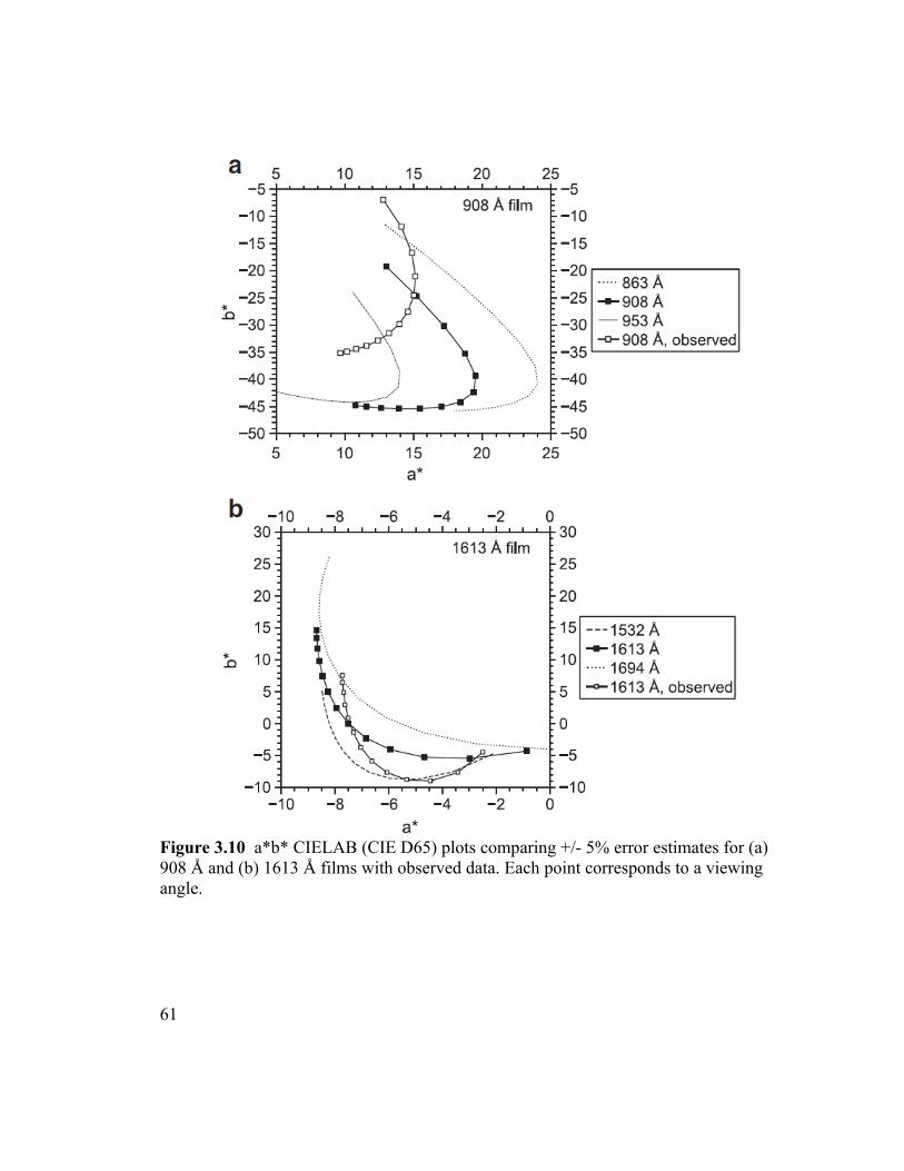
Figure 3.10 a*b* CIELAB (CIE D65) plots comparing +/- 5% error estimates for (a) 908 Å and (b) 1613 Å films with observed data. Each point corresponds to a viewing angle.
61
Figure 3.9 shows some results for nine different thicknesses. It can be seen that the 0
Å coating (bulk Si) produces the least iridescence. This sample appears grey with a very
slight blue cast, and the colour variation with angle is only 3 units along the blue axis,
making it barely detectable by eye. For bare Si, the measurements agree with the
predictions. The 908 Å sample exhibits the largest iridescence. The colour goes from
very chromatic purplish blue, at 10° viewing, to a greyish purple pink at 70° viewing. It
can be observed that it is for the highly iridescent coatings that the difference between the
measurement and the prediction is the highest. The iridescence appears much
pronounced for the prediction, and the colour itself at some given angle can differ by
more than 20 units.
To determine if the discrepancy between observed and calculated data was simply due
to film thickness measurement error introduced by the ellipsometer, additional plots of
+/- 5% thicknesses were calculated for 908 Å and 1613 Å (Figure 3.10 a) and b)
respectively). These plots illustrate that while a 5% measurement error would have a
significant impact on the shape of the curves, the induced variations would not be in the
directions of the observed discrepancies. Instead it is most likely the dispersion curves of
the deposited material are responsible for these discrepancies.
This comparison demonstrates that for cosmetic applications, in which the final colour
is of primary concern, it is important to actually measure the end product and not rely just
on predictions.
62
3.5 Conclusions
A robot-based gonioreflectometer has been used to analyze the colours resulting from
thin films of aluminum oxide deposited by ALD on silicon with unprecedented precision.
A comparison has been made between the experimental reflectivities obtained and those
predicted by software simulations. For the range of thicknesses studied (0 - 1613 Å), the
largest disagreement between theory and experiment was observed for the films of
intermediate thicknesses, which are also the most iridescent. The largest disagreement
for a given sample was most often found at short wavelengths, with 7 of the 12 samples
exhibiting their largest deviations from the model between the wavelengths of 380 and
445 nm. An analysis of the data with respect to angle showed that the disagreements
were higher at near-normal angles of reflection (≤15°). This is not totally surprising:
while one might expect the larger deviations to occur at more oblique angles, where the
path length through the film is longest, the reflection itself is dominated by interference
between phase shifted wave fronts, and this phase shift decreases with reflection angle.
Further studies are necessary to determine the dispersion curves of the deposited films,
which should allow for a more accurate simulation of the system. It is very likely that the
dielectric constants of the films deviate from the literature values as ALD processes are
known to deposit films with densities that differ from bulk values, depending on process
parameters.
63
Chapter 4 - Characterization and assessment of a novel hybrid
organic/inorganic metal-insulator-semiconductor structure for
photovoltaic applications
Modified from original manuscript, published as: Svetlana Demtchenko*a, Peter Gordonb, Sean Barryb, N. Garry Tarra, Steven McGarrya “Characterization and assessment of a novel hybrid organic/inorganic metal-insulator-semiconductor structure for photovoltaic applications” Proc.SPIE 7750, 2010, DOI 10.1117/12.871360. aDepartment of Electronics, Carleton University, OttawabDepartment of Chemistry, Carleton University, Ottawa
4.1 Abstract
Hybrid organic/inorganic photovoltaic devices have recently emerged as a possible
solution to the stability, charge transfer and mobility issues that have been limiting the
lifetimes and efficiencies of organic solar cells. The purpose of the project presented here
is to assess the potential of a new hybrid metal-insulator-semiconductor (MIS)
photovoltaic device design developed at Carleton University. The silicon substrate is
nanostructured with a wet chemical etch resulting in about 1:1 aspect ratio structures of
roughly 300 nm in size. The interface is passivated with a thin dielectric tunnel barrier of
alumina or silica. A layer of transparent conducting polymer, Poly(3,4-
ethylenedioxythiophene) (PEDOT), is added through in-situ polymerization. The
structure is then completed with a printed silver/polymer composite collection electrode.
The electrical current-voltage (I-V) and capacitance-voltage (C-V) characteristics along
with the effect of nanostructuring the substrate on the performance of such a solar cell is
64
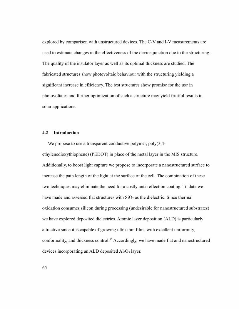
explored by comparison with unstructured devices. The C-V and I-V measurements are
used to estimate changes in the effectiveness of the device junction due to the structuring.
The quality of the insulator layer as well as its optimal thickness are studied. The
fabricated structures show photovoltaic behaviour with the structuring yielding a
significant increase in efficiency. The test structures show promise for the use in
photovoltaics and further optimization of such a structure may yield fruitful results in
solar applications.
4.2 Introduction
We propose to use a transparent conductive polymer, poly(3,4-
ethylenedioxythiophene) (PEDOT) in place of the metal layer in the MIS structure.
Additionally, to boost light capture we propose to incorporate a nanostructured surface to
increase the path length of the light at the surface of the cell. The combination of these
two techniques may eliminate the need for a costly anti-reflection coating. To date we
have made and assessed flat structures with SiO2 as the dielectric. Since thermal
oxidation consumes silicon during processing (undesirable for nanostructured substrates)
we have explored deposited dielectrics. Atomic layer deposition (ALD) is particularly
attractive since it is capable of growing ultra-thin films with excellent uniformity,
conformality, and thickness control.83 Accordingly, we have made flat and nanostructured
devices incorporating an ALD deposited Al2O3 layer.
65
A small set of cells were fabricated and tested. The fabrication flow was designed to
use a vacuum-less process aimed at further reducing the cost of such a device. Our efforts
in assessing the feasibility of such structures for photovoltaic applications are described
herein.
The open circuit voltage (Voc) of an MIS device depends on the photogenerated
current (Isc) and the reverse saturation current (Io) as follows98:
V oc=nkTq
ln (I sc
I o
+1)
Thus to increase the open circuit voltage and the overall performance of the cell, the
reverse saturation current has to be minimized.
There are a number of schemes known to result in a reduced reverse saturation current
in an MIS type structure. To achieve this effect the metal/semiconductor barrier height
can be increased, the probability of the majority carriers tunneling though the insulator
barrier can be decreased, or surface states at the semiconductor/insulator interface can be
included that preferentially capture majority carriers.99 In our devices the insulator layer
serves to increase the barrier height for thermionic emission and the probability of
majority carrier tunneling is reduced by the inversion of the semiconductor surface, since
the tunneling probability depends on the population of states on both sides of the
junction.
66
Such inversion at the interface will also ensure that the interfacial states are occupied
by the minority carriers and thus reduce the surface recombination due to the interfacial
states. The inversion condition can be achieved with high work function metals for n-type
material. For silicon substrates the metal work function has to be72:
φm≥ χ+Eg
φm≥4.05 eV +1.1eV
φm≥5.15 eV
were χ is the electron affinity of silicon and Eg is silicon's band gap. This condition is
satisfied for PEDOT:PSS with an accepted work function of φm ≈ 5.2 eV.100
Thus the structure of such a hybrid MIS device is as shown in Figure 4.1. The n-type
Si substrate captures the light. The surface of the substrate can be flat or structured as
shown in the figure. Even though an ordered structuring is depicted, a random structuring
would result in better light capture, which is what our structuring process achieves. On
top of the substrate surface an ultra-thin layer of dielectric is grown or deposited,
followed by PEDOT. The structure is completed with a screen printed finder-grid
contacts.
67
Figure 4.1 Representations of the hybrid MIS device. Flat device is shown in (a), nanostructured device shown in (b) and band diagram in (c).
For an optimal device with current-voltage characteristics approaching those of a p-n
junction, the insulator layer must remain thin, less than 20 Å.71,72 As the thickness of the
insulator influences the tunnelling probability of minority carriers as well as the majority
carriers, as the Voc increases with the increasing thickness, the Isc will decrease. Thus there
exists an optimal thickness of the insulating layer for the best performance of a
photovoltaic device.
4.3 Experimental
The starting material used was n-type Si with 1-10 Ω·cm resistivity. The wafers were
cleaned before processing. Three different types of structures where fabricated and
examined: flat devices with thermally grown oxide, flat devices with Al2O3 grown by
68
ALD, and devices on nanostructured substrates with ALD Al2O3. The fabrication for each
structure is detailed below.
Flat devices with thermally grown oxide
The front side of the wafers was treated with HF vapour to remove any native oxide.
After the HF treatment the wafers were immediately placed in an oxidation furnace for 10
min at various temperatures (450 °C – 550 °C) to grow increasing thicknesses of SiO2.
Oxidation was followed by deposition of backside aluminum by evaporation.
PEDOT:PSS (Clevios PH750 supplied by H.C. Starck) was spin-cast on top of the grown
oxide. The structure was completed by screen printing silver ink (Dupont 5028). A
finished wafer of devices is shown in Figure 4.2(a). The wafers were stored in a dry
nitrogen box or under vacuum between processing steps to avoid undesirable continued
growth of the oxide layer.
Flat devices with ALD Al2O3
The back side of the wafer was metallized with aluminum and Al2O3 was grown by
ALD on the front surface. The samples were then annealed at 400 °C in forming gas (N2
with 5% H2) to activate the passivation of silicon by Al2O3 as was found necessary by
Dingemans et al.; forming gas was used instead of N2 to take advantage of hydrogen
passivation of dangling bonds on the silicon surface as the chemical passivation by Al2O3
at such small layer thicknesses is deemed ineffective.101 High conductivity PEDOT:PSS
69
(Clevios FET supplied by H.C. Starck) was spun down on top of the alumina. The
structure was completed by screen printing silver ink (Dupont 5028) as before.
Nanostructured devices
The nanostructuring was achieved with a wet chemical etch based on the procedure
reported by Branz et al.102 The colloidal gold (5 nm particle size) solution (purchased
from Sigma-Aldrich; #G1402) was dried on the silicon substrate overnight at room
temperature. The substrates were not heated to minimize the aggregation of gold
particles. Thus prepared substrates were sonicated in HF:H2O2:H2O (1:5:2) to effect the
metal-assisted chemical etch (MACE). MACE is a technique for etching silicon or other
semiconductor surfaces, typically using a surface layer of silver or gold (nanoparticulate
or porous) and a solution of HF and an oxidant.103,34,104,105 The nanostructured substrate
was then washed in aqua regia to remove the remaining gold particles. An aluminum
back contact was evaporated on to the back of the substrate and
sintered at 400°C for 10 min in H2. Various thicknesses of Al2O3 (~ 4-14 Å) were grown
by ALD. The PEDOT was deposited in situ from EDOT monomer (Baytron M) using
Fe(III) tosylate in butanol (Baytron CB-40) as an oxidizer. Silver ink was deposited on
top of the structure as the current collecting electrode. A set of flat samples was processed
in parallel for comparison.
Testing the devices
70
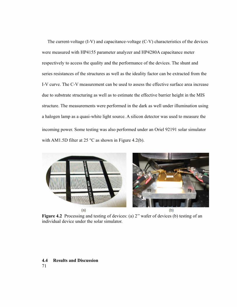
The current-voltage (I-V) and capacitance-voltage (C-V) characteristics of the devices
were measured with HP4155 parameter analyzer and HP4280A capacitance meter
respectively to access the quality and the performance of the devices. The shunt and
series resistances of the structures as well as the ideality factor can be extracted from the
I-V curve. The C-V measurement can be used to assess the effective surface area increase
due to substrate structuring as well as to estimate the effective barrier height in the MIS
structure. The measurements were performed in the dark as well under illumination using
a halogen lamp as a quasi-white light source. A silicon detector was used to measure the
incoming power. Some testing was also performed under an Oriel 92191 solar simulator
with AM1.5D filter at 25 °C as shown in Figure 4.2(b).
Figure 4.2 Processing and testing of devices: (a) 2’’ wafer of devices (b) testing of an individual device under the solar simulator.
4.4 Results and Discussion71
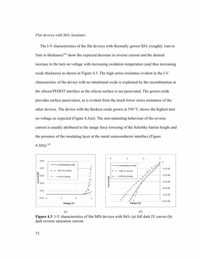
Flat devices with SiO2 insulator
The I-V characteristics of the flat devices with thermally grown SiO2 (roughly 1nm to
5nm in thickness)106 show the expected decrease in reverse current and the desired
increase in the turn on voltage with increasing oxidation temperature (and thus increasing
oxide thickness) as shown in Figure 4.3. The high series resistance evident in the I-V
characteristic of the device with no intentional oxide is explained by the recombination at
the silicon/PEDOT interface as the silicon surface is not passivated. The grown oxide
provides surface passivation, as is evident from the much lower series resistance of the
other devices. The device with the thickest oxide grown at 550 °C shows the highest turn
on voltage as expected (Figure 4.3(a)). The non-saturating behaviour of the reverse
current is usually attributed to the image force lowering of the Schottky barrier height and
the presence of the insulating layer at the metal semiconductor interface (Figure
4.3(b)).107
Figure 4.3 I-V characteristics of flat MIS devices with SiO2 (a) full dark IV curves (b) dark reverse saturation current.
72
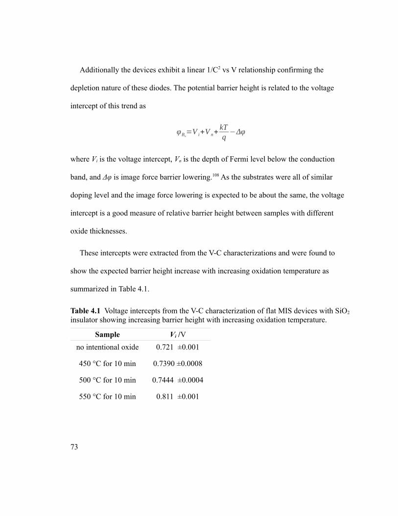
Additionally the devices exhibit a linear 1/C2 vs V relationship confirming the
depletion nature of these diodes. The potential barrier height is related to the voltage
intercept of this trend as
φBn=V i+V n+
kTq
−Δφ
where Vi is the voltage intercept, Vn is the depth of Fermi level below the conduction
band, and Δφ is image force barrier lowering.108 As the substrates were all of similar
doping level and the image force lowering is expected to be about the same, the voltage
intercept is a good measure of relative barrier height between samples with different
oxide thicknesses.
These intercepts were extracted from the V-C characterizations and were found to
show the expected barrier height increase with increasing oxidation temperature as
summarized in Table 4.1.
Table 4.1 Voltage intercepts from the V-C characterization of flat MIS devices with SiO2 insulator showing increasing barrier height with increasing oxidation temperature.
Sample Vi /V
no intentional oxide 0.721 ±0.001
450 °C for 10 min 0.7390 ±0.0008
500 °C for 10 min 0.7444 ±0.0004
550 °C for 10 min 0.811 ±0.001
73
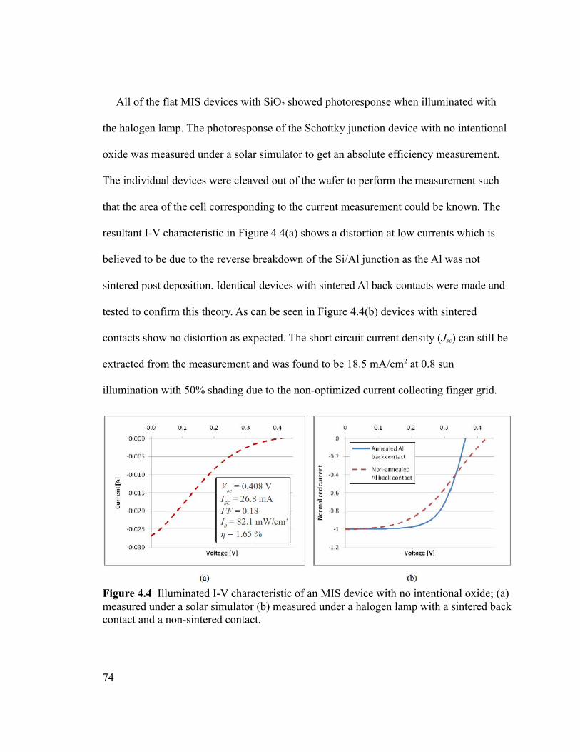
All of the flat MIS devices with SiO2 showed photoresponse when illuminated with
the halogen lamp. The photoresponse of the Schottky junction device with no intentional
oxide was measured under a solar simulator to get an absolute efficiency measurement.
The individual devices were cleaved out of the wafer to perform the measurement such
that the area of the cell corresponding to the current measurement could be known. The
resultant I-V characteristic in Figure 4.4(a) shows a distortion at low currents which is
believed to be due to the reverse breakdown of the Si/Al junction as the Al was not
sintered post deposition. Identical devices with sintered Al back contacts were made and
tested to confirm this theory. As can be seen in Figure 4.4(b) devices with sintered
contacts show no distortion as expected. The short circuit current density (Jsc) can still be
extracted from the measurement and was found to be 18.5 mA/cm2 at 0.8 sun
illumination with 50% shading due to the non-optimized current collecting finger grid.
Figure 4.4 Illuminated I-V characteristic of an MIS device with no intentional oxide; (a) measured under a solar simulator (b) measured under a halogen lamp with a sintered back contact and a non-sintered contact.
74
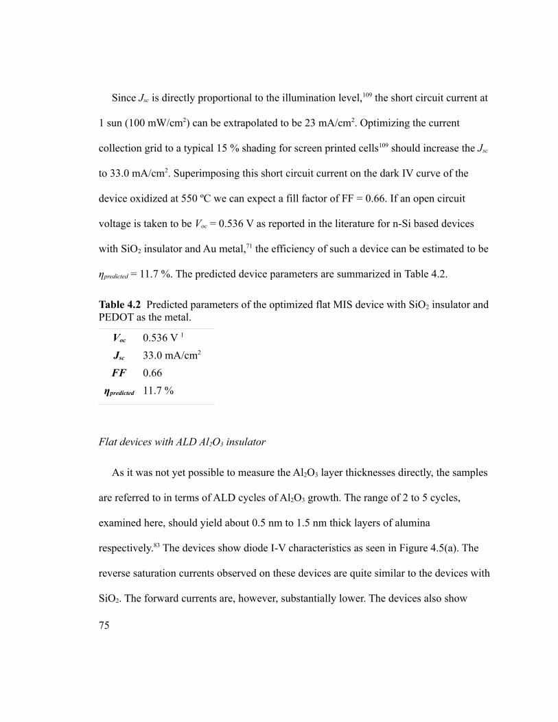
Since Jsc is directly proportional to the illumination level,109 the short circuit current at
1 sun (100 mW/cm2) can be extrapolated to be 23 mA/cm2. Optimizing the current
collection grid to a typical 15 % shading for screen printed cells109 should increase the Jsc
to 33.0 mA/cm2. Superimposing this short circuit current on the dark IV curve of the
device oxidized at 550 ºC we can expect a fill factor of FF = 0.66. If an open circuit
voltage is taken to be Voc = 0.536 V as reported in the literature for n-Si based devices
with SiO2 insulator and Au metal,71 the efficiency of such a device can be estimated to be
ηpredicted = 11.7 %. The predicted device parameters are summarized in Table 4.2.
Table 4.2 Predicted parameters of the optimized flat MIS device with SiO2 insulator and PEDOT as the metal.
Voc 0.536 V 1
Jsc 33.0 mA/cm2
FF 0.66
ηpredicted 11.7 %
Flat devices with ALD Al2O3 insulator
As it was not yet possible to measure the Al2O3 layer thicknesses directly, the samples
are referred to in terms of ALD cycles of Al2O3 growth. The range of 2 to 5 cycles,
examined here, should yield about 0.5 nm to 1.5 nm thick layers of alumina
respectively.83 The devices show diode I-V characteristics as seen in Figure 4.5(a). The
reverse saturation currents observed on these devices are quite similar to the devices with
SiO2. The forward currents are, however, substantially lower. The devices also show
75
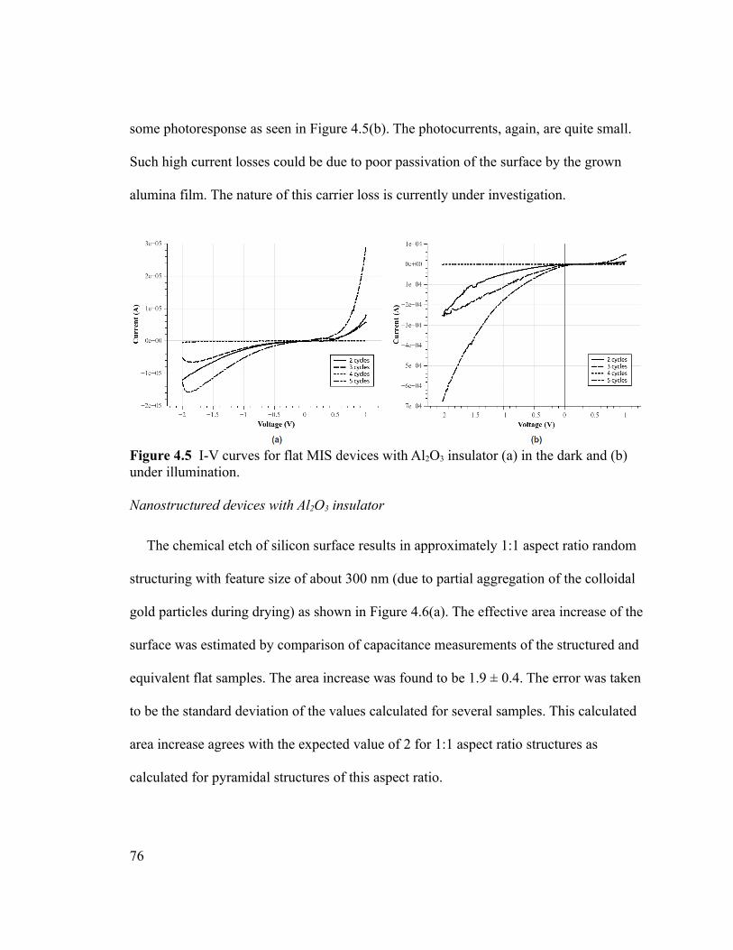
some photoresponse as seen in Figure 4.5(b). The photocurrents, again, are quite small.
Such high current losses could be due to poor passivation of the surface by the grown
alumina film. The nature of this carrier loss is currently under investigation.
Figure 4.5 I-V curves for flat MIS devices with Al2O3 insulator (a) in the dark and (b) under illumination.
Nanostructured devices with Al2O3 insulator
The chemical etch of silicon surface results in approximately 1:1 aspect ratio random
structuring with feature size of about 300 nm (due to partial aggregation of the colloidal
gold particles during drying) as shown in Figure 4.6(a). The effective area increase of the
surface was estimated by comparison of capacitance measurements of the structured and
equivalent flat samples. The area increase was found to be 1.9 ± 0.4. The error was taken
to be the standard deviation of the values calculated for several samples. This calculated
area increase agrees with the expected value of 2 for 1:1 aspect ratio structures as
calculated for pyramidal structures of this aspect ratio.
76
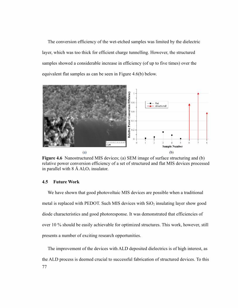
The conversion efficiency of the wet-etched samples was limited by the dielectric
layer, which was too thick for efficient charge tunnelling. However, the structured
samples showed a considerable increase in efficiency (of up to five times) over the
equivalent flat samples as can be seen in Figure 4.6(b) below.
Figure 4.6 Nanostructured MIS devices; (a) SEM image of surface structuring and (b) relative power conversion efficiency of a set of structured and flat MIS devices processed in parallel with 8 Å Al2O3 insulator.
4.5 Future Work
We have shown that good photovoltaic MIS devices are possible when a traditional
metal is replaced with PEDOT. Such MIS devices with SiO2 insulating layer show good
diode characteristics and good photoresponse. It was demonstrated that efficiencies of
over 10 % should be easily achievable for optimized structures. This work, however, still
presents a number of exciting research opportunities.
The improvement of the devices with ALD deposited dielectrics is of high interest, as
the ALD process is deemed crucial to successful fabrication of structured devices. To this
77
end the ALD insulator process is still in development - other methods, precursors and
compositions are under investigation.
To achieve higher aspect ratio structures self-masking electron cyclotron resonance
reactive ion etching (ECR RIE) has been used. Structures with 10:1 aspect ratio were
fabricated. The testing of the devices made on these substrates is ongoing. Additionally,
to create finer structures with a wet chemical etch an alternative gold deposition method
will be attempted, known to result in a uniform controllable particle density on the
surface.110
It is expected that spin coating of PEDOT:PSS will be incompatible with the high
aspect ratio structures that we hope to use on the substrates in the future. To mitigate this
problem we will deposit PEDOT by vapour phase polymerization (VPP). Such deposition
method is known to result in conformal coverage with well controlled thickness and
conductivities of over 1000 S/cm.111,76,112 The assembly of the deposition system is in
progress.
4.6 Acknowledgements
The authors would like to thank Rob Vandusen, Carol Adams, and Rick Adams for
their invaluable help with the processing of the samples as well as Karin Hinzer and
Mark Yandt for the use of their solar simulator. This project is financially supported by
Natural Sciences and Engineering Research Council of Canada (NSERC).
78
Chapter 5 - Chemical vapour deposition of In2O3 thin films from a tris-
guanidinate indium precursor
Modified from original manuscript, published as: Barry, S. T.a; Gordon, P. G.a; Ward, M. J.b; Heikkila, M. J.c; Monillas, W. H.d; Yap, G. P.d; Ritala, M.c; Leskelä, M.c Dalton transactions 2011, 40, 9425–30.aDepartment of Chemistry, Carleton University, Ottawa, Canada K1S 5B6bDepartment of Chemistry, University of Western Ontario, London, ON, Canada N6A 5B7 cLaboratory of Inorganic Chemistry, Department of Chemistry, University of Helsinki, P.O. Box 55, FI-00014, Finland dDepartment of Chemistry and Biochemistry, University of Delaware, Newark, 19716, Delaware, U. S. A.Accepted 17th June 2011, first published on the web 16th August 2011
5.1 Abstract
A new homoleptic sublimable indium(III) guanidinate, (In[(NiPr)2CNMe2]3 (1), was
synthesized from a facile high-yield procedure. Compound 1 crystallized as a P space
group ; a = 10.5989(14) Å, b = 11.0030(15) Å, c = 16.273(2) Å, α = 91.190(2)°, β =
96.561(2)°, γ = 115.555(2)°; R = 3.50%. Thermogravimetric analysis showed 1 to
produce elemental indium as a residual mass. Thermolysis in a sealed NMR tube showed
carbodiimide and protonated dimethyl amine by 1H NMR. Chemical vapour deposition
experiments above 275 °C with air as the reactant gas showed 1 to readily deposit cubic
indium oxide with good transparency.
79
5.2 Results and Discussion
Precursor synthesis
The precursor was synthesized via carbodiimide insertion into lithium dimethylamide
to form the lithiated guanidinate [(Me2N)C(NiPr)2]Li which then underwent salt
metathesis with InCl3 to produce 1 in excellent yield. The 1H NMR spectrum of 1
contains a septet for the isopropyl methine proton, a singlet for the exocyclic amide
methyl groups, and two well-resolved doublets for the diastereotopic methyl groups from
the isopropyl . Our previous research has shown a range of behaviour for these isopropyl
groups at different metal centres, where a single environment is found for less sterically
crowded centres, and two environments are found where steric effects prevent exchange
of these groups.113 Thus, the two doublets indicate a sterically crowded metal centre, as
previously seen for the aluminum and gallium analogues of 1.
In the solid state, 1 (see Table
5.1), isostructurally with previously reported Al and Ga analogues,113 and isomorphously
with Y, Gd, and Dy analogues (Figure 5.1).114 The indium ion displays distorted trigonal
prism coordination geometry with a molecular three-fold axis of symmetry that does not
coincide with any crystallographic symmetry element. Within error the bond distances
and angles corresponding to chemically equivalent moieties in each of the ligands are
statistically indistinguishable from each other. This is consistent to what is observed in
the solution NMR. The nitrogen atoms in the exocyclic amide groups and the chelating
80
nitrogen atoms each exhibit planar geometry suggesting that the π system in the chelate
rings extends to the exocyclic amides. However, the C–N bond lengths in the chelate
rings (typically 1.33 Å) are shorter than the C–N bond length from the exocyclic amide to
the bridgehead carbon (typically 1.40 Å), demonstrating that the π system resides mainly
in the chelate metallocycle (see Table 5.2). This is not surprising, since the exocyclic
amide groups in the ligands of 1 were rotated out of the metallocycle plane by 40.0°–
47.1°. There exists a cos2θ relationship for the overlap of p-orbitals in such
arrangements.115
81
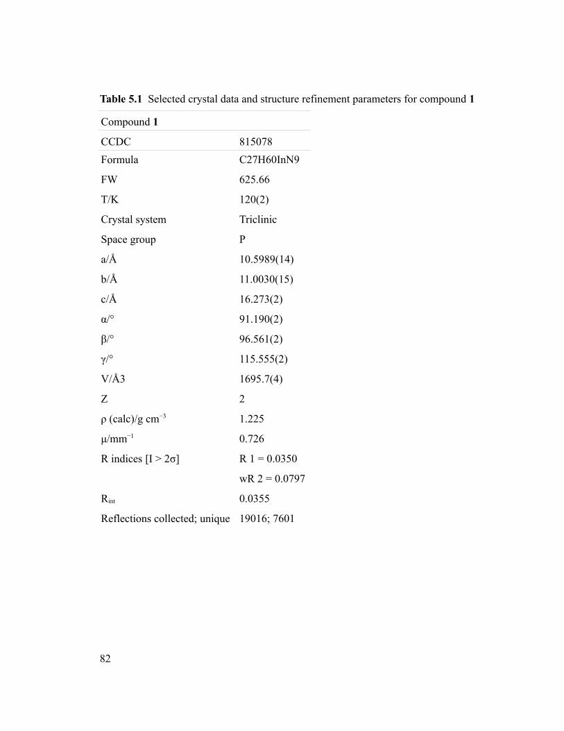
Table 5.1 Selected crystal data and structure refinement parameters for compound 1
Compound 1
CCDC 815078
Formula C27H60InN9
FW 625.66
T/K 120(2)
Crystal system Triclinic
Space group P
a/Å 10.5989(14)
b/Å 11.0030(15)
c/Å 16.273(2)
α/° 91.190(2)
β/° 96.561(2)
γ/° 115.555(2)
V/Å3 1695.7(4)
Z 2
ρ (calc)/g cm−3 1.225
μ/mm−1 0.726
R indices [I > 2σ] R 1 = 0.0350
wR 2 = 0.0797
Rint 0.0355
Reflections collected; unique 19016; 7601
82
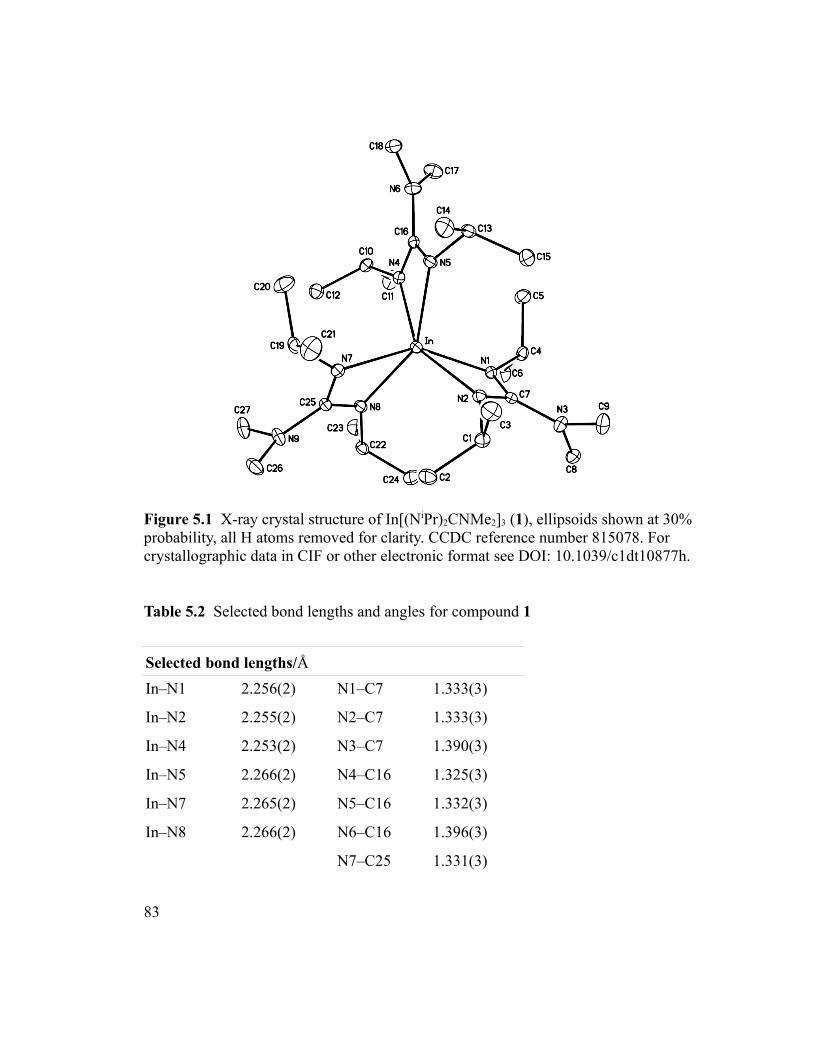
Figure 5.1 X-ray crystal structure of In[(NiPr)2CNMe2]3 (1), ellipsoids shown at 30% probability, all H atoms removed for clarity. CCDC reference number 815078. For crystallographic data in CIF or other electronic format see DOI: 10.1039/c1dt10877h.
Table 5.2 Selected bond lengths and angles for compound 1
Selected bond lengths/Å
In–N1 2.256(2) N1–C7 1.333(3)
In–N2 2.255(2) N2–C7 1.333(3)
In–N4 2.253(2) N3–C7 1.390(3)
In–N5 2.266(2) N4–C16 1.325(3)
In–N7 2.265(2) N5–C16 1.332(3)
In–N8 2.266(2) N6–C16 1.396(3)
N7–C25 1.331(3)
83
N8–C25 1.326(3)
N9–C25 1.407(3)
Selected bond angles/°
N2–In–N1 59.45(7) N1–C7–N2 114.1(2)
N4–In–N5 59.30(7) N4–C16–N5 114.6(2)
N8–In–N7 59.30(7) N7–C25–N8 115.0(2)
Sum of angles/°
N1 354 ± 2 N5 354 ± 2
N2 354 ± 2 N6 360 ± 2
N3 360 ± 2 N7 354 ± 2
N4 355 ± 2 N8 355 ± 2
N9 357 ± 2
84
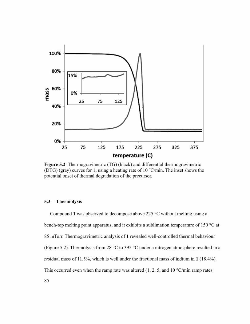
Figure 5.2 Thermogravimetric (TG) (black) and differential thermogravimetric (DTG) (gray) curves for 1, using a heating rate of 10 °C/min. The inset shows the potential onset of thermal degradation of the precursor.
5.3 Thermolysis
Compound 1 was observed to decompose above 225 °C without melting using a
bench-top melting point apparatus, and it exhibits a sublimation temperature of 150 °C at
85 mTorr. Thermogravimetric analysis of 1 revealed well-controlled thermal behaviour
(Figure 5.2). Thermolysis from 28 °C to 395 °C under a nitrogen atmosphere resulted in a
residual mass of 11.5%, which is well under the fractional mass of indium in 1 (18.4%).
This occurred even when the ramp rate was altered (1, 2, 5, and 10 °C/min ramp rates
85
were tried). A flame test of the residual grey powder confirmed the presence of indium
(intense indigo colour). Although the differential thermogravimetric (DTG) curve
suggests a very clean sublimation, it seems that the compound undergoes both
sublimation and decomposition in this region.
A thermal 1H NMR experiment was employed where a sealed thick-walled NMR tube
was subjected to increasing temperature from room temperature to 170 °C, with spectra
collected at appropriate intervals. At room temperature no diisopropylcarbodiimide (CDI)
was observed in the 1H NMR spectrum of 1. At 110 °C signals corresponding to CDI as
well as peaks for dimethyl amine were found. This onset of thermolysis may correspond
to the very small peak seen in the DTG curve (inset in Figure 5.2), however there is no
correlation between the mass loss in the TG and this fragment of the ligand. A more
detailed thermolysis study would be required to relate these experiments to each other,
and this is beyond the scope of the present study.
By 140 °C the CDI and dimethyl amine peaks had grown further and remained in
fairly constant proportion to the peaks for 1 up to 170 °C, and a precipitate was apparent
in the NMR tube. This suggests that free guanidine was produced and subsequently
decomposed to CDI and amine . This has been seen at similar temperatures with a copper
guanidinate.116 This is interesting since all of these data suggest that 1 will undergo
thermal decomposition and might deposit indium oxide quite easily using air as an
oxygen source. More experimental work is ongoing to better understand the mechanism.
86
5.4 Film depositions and characterization
When 1 was used as a CVD precursor, it was found to deposit indium oxide using air
or 10% O2 in N2 as the reactant gas. Indium metal, reduced by the ligand, was deposited
under vacuum with no reactant gas. The deposition in both cases needed to occur above
275 °C to show significant film growth, and so the deposition of indium metal was
difficult to quantify; at that temperature indium metal is liquid and did not remain on the
substrate. Thus, only the deposition of indium oxide was explored in depth. Interestingly,
the onset of growth is lower than has been typically seen for CVD of indium oxide.21–24
When the deposition was undertaken at 350 °C using 1 as the precursor and air as the
reactant gas (Table 5.3, runs a–h), crystalline cubic indium oxide was formed, giving a
lattice parameter of 10.120 Å (acquired by Rietveld refinement using MAUD software117)
while the value in PDF card 6-416 is 10.118 Å. (Figure 5.3). It was also interesting to
note that crystalline indium metal could be detected by XRD in run g. Modelling the
integration of the indium metal peaks against the peaks of indium oxide showed that this
impurity was present in 1–2% abundance. This suggests that 1 thermally decomposed to a
reduced indium state, and then likely re-oxidized in air to produce indium(III) oxide. This
supports the thermolysis experiments presented above. An X-ray photoelectron spectrum
(XPS) of the film supported the characterization of the film as indium oxide (Figure 5.4),
and energy dispersive X-ray (EDS ) showed both indium and oxygen (as well as silicon
from the substrate) to be present in the film. The XPS spectra were calibrated using the C
1s peak as a reference, setting it to 284 eV. The oxygen signal consisted of two
87
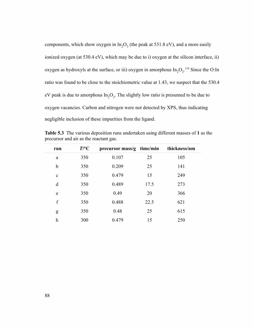
components, which show oxygen in In2O3 (the peak at 531.8 eV), and a more easily
ionized oxygen (at 530.4 eV), which may be due to i) oxygen at the silicon interface, ii)
oxygen as hydroxyls at the surface, or iii) oxygen in amorphous In2O3.118 Since the O:In
ratio was found to be close to the stoichiometric value at 1.43, we suspect that the 530.4
eV peak is due to amorphous In2O3. The slightly low ratio is presumed to be due to
oxygen vacancies. Carbon and nitrogen were not detected by XPS, thus indicating
negligible inclusion of these impurities from the ligand.
Table 5.3 The various deposition runs undertaken using different masses of 1 as the precursor and air as the reactant gas.
run T/°C precursor mass/g time/min thickness/nm
a 350 0.107 25 105
b 350 0.209 25 141
c 350 0.479 15 249
d 350 0.489 17.5 273
e 350 0.49 20 366
f 350 0.488 22.5 621
g 350 0.48 25 615
h 300 0.479 15 250
88
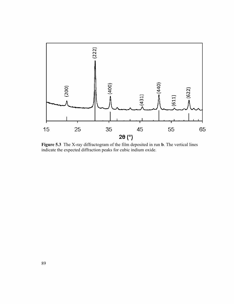
Figure 5.3 The X-ray diffractogram of the film deposited in run b. The vertical lines indicate the expected diffraction peaks for cubic indium oxide.
89
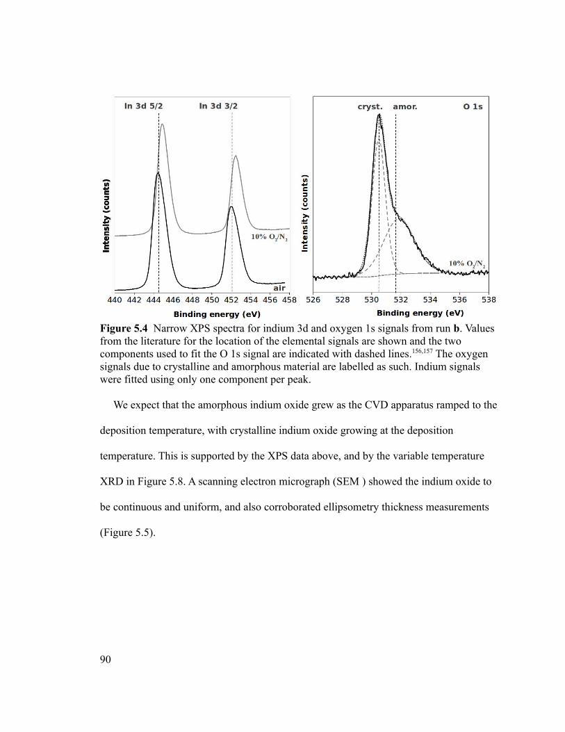
Figure 5.4 Narrow XPS spectra for indium 3d and oxygen 1s signals from run b. Values from the literature for the location of the elemental signals are shown and the two components used to fit the O 1s signal are indicated with dashed lines.156,157 The oxygen signals due to crystalline and amorphous material are labelled as such. Indium signals were fitted using only one component per peak.
We expect that the amorphous indium oxide grew as the CVD apparatus ramped to the
deposition temperature, with crystalline indium oxide growing at the deposition
temperature. This is supported by the XPS data above, and by the variable temperature
XRD in Figure 5.8. A scanning electron micrograph (SEM ) showed the indium oxide to
be continuous and uniform, and also corroborated ellipsometry thickness measurements
(Figure 5.5).
90
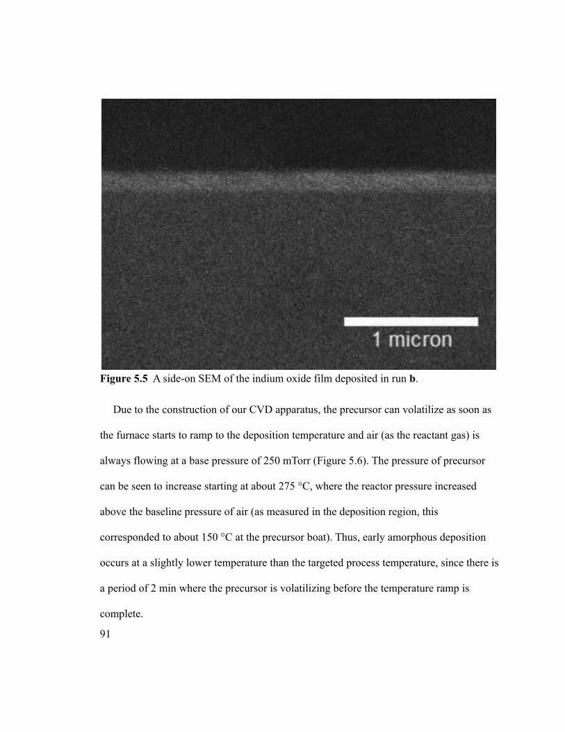
Figure 5.5 A side-on SEM of the indium oxide film deposited in run b.
Due to the construction of our CVD apparatus, the precursor can volatilize as soon as
the furnace starts to ramp to the deposition temperature and air (as the reactant gas) is
always flowing at a base pressure of 250 mTorr (Figure 5.6). The pressure of precursor
can be seen to increase starting at about 275 °C, where the reactor pressure increased
above the baseline pressure of air (as measured in the deposition region, this
corresponded to about 150 °C at the precursor boat). Thus, early amorphous deposition
occurs at a slightly lower temperature than the targeted process temperature, since there is
a period of 2 min where the precursor is volatilizing before the temperature ramp is
complete.
91
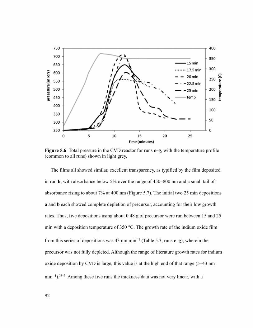
Figure 5.6 Total pressure in the CVD reactor for runs c–g, with the temperature profile (common to all runs) shown in light grey.
The films all showed similar, excellent transparency, as typified by the film deposited
in run b, with absorbance below 5% over the range of 450–800 nm and a small tail of
absorbance rising to about 7% at 400 nm (Figure 5.7). The initial two 25 min depositions
a and b each showed complete depletion of precursor, accounting for their low growth
rates. Thus, five depositions using about 0.48 g of precursor were run between 15 and 25
min with a deposition temperature of 350 °C. The growth rate of the indium oxide film
from this series of depositions was 43 nm min−1 (Table 5.3, runs c–g), wherein the
precursor was not fully depleted. Although the range of literature growth rates for indium
oxide deposition by CVD is large, this value is at the high end of that range (5–43 nm
min−1).21–24 Among these five runs the thickness data was not very linear, with a
92
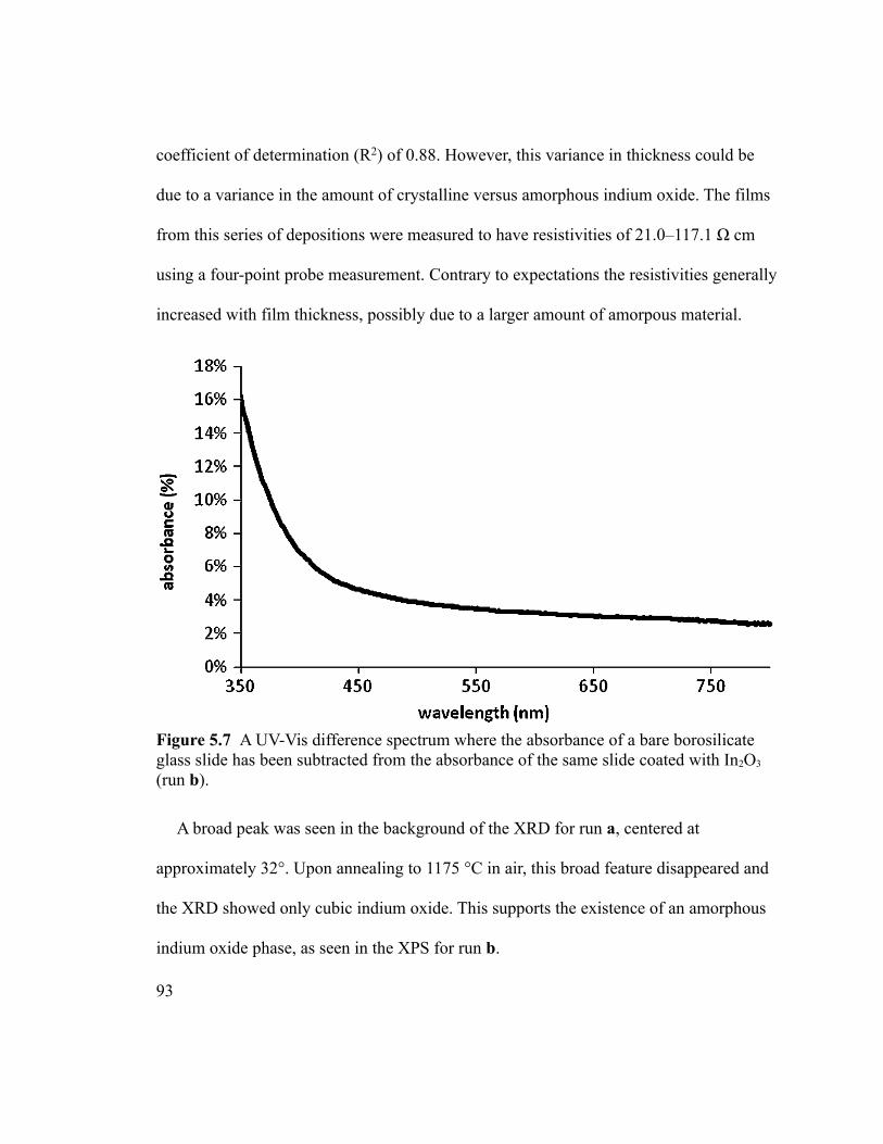
coefficient of determination (R2) of 0.88. However, this variance in thickness could be
due to a variance in the amount of crystalline versus amorphous indium oxide. The films
from this series of depositions were measured to have resistivities of 21.0–117.1 Ω cm
using a four-point probe measurement. Contrary to expectations the resistivities generally
increased with film thickness, possibly due to a larger amount of amorpous material.
Figure 5.7 A UV-Vis difference spectrum where the absorbance of a bare borosilicate glass slide has been subtracted from the absorbance of the same slide coated with In2O3 (run b).
A broad peak was seen in the background of the XRD for run a, centered at
approximately 32°. Upon annealing to 1175 °C in air, this broad feature disappeared and
the XRD showed only cubic indium oxide. This supports the existence of an amorphous
indium oxide phase, as seen in the XPS for run b.
93
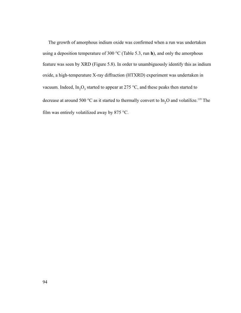
The growth of amorphous indium oxide was confirmed when a run was undertaken
using a deposition temperature of 300 °C (Table 5.3, run h), and only the amorphous
feature was seen by XRD (Figure 5.8). In order to unambiguously identify this as indium
oxide, a high-temperature X-ray diffraction (HTXRD) experiment was undertaken in
vacuum. Indeed, In2O3 started to appear at 275 °C, and these peaks then started to
decrease at around 500 °C as it started to thermally convert to In2O and volatilize.119 The
film was entirely volatilized away by 875 °C.
94
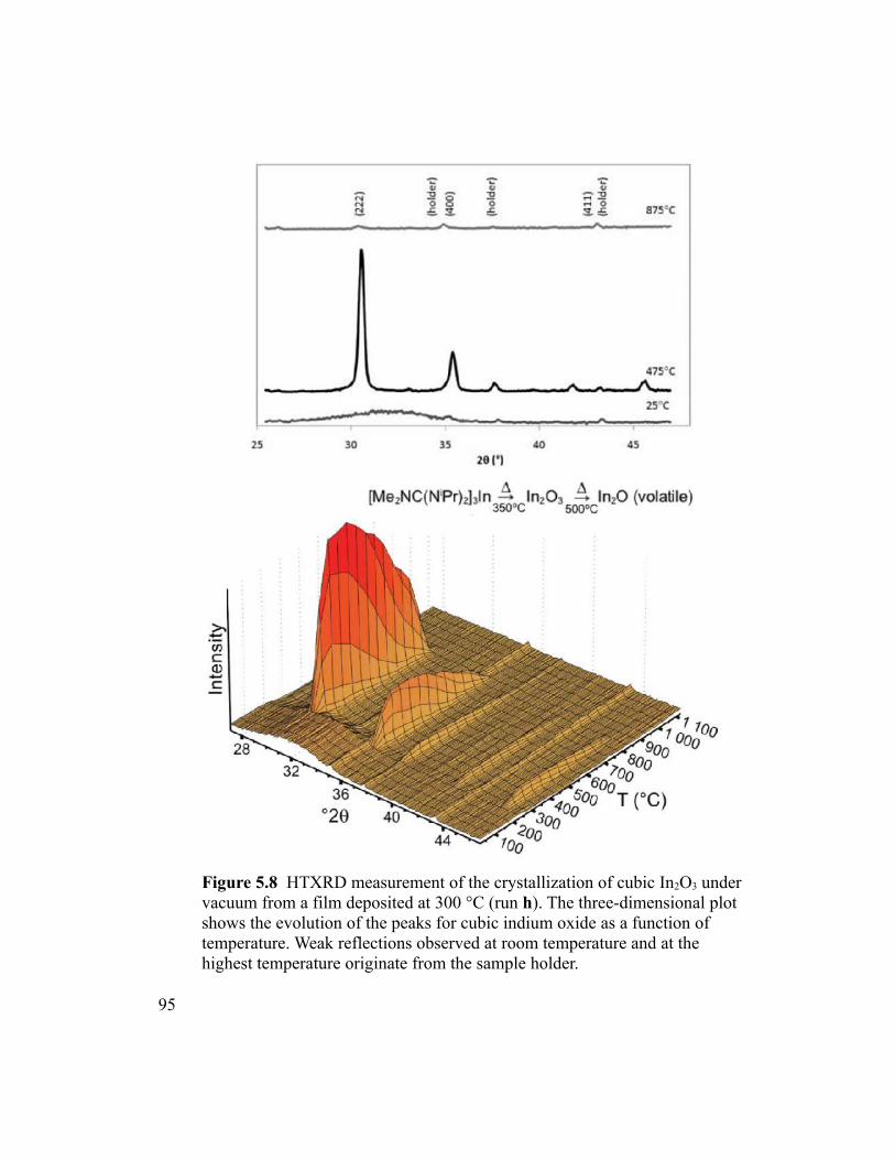
Figure 5.8 HTXRD measurement of the crystallization of cubic In2O3 under vacuum from a film deposited at 300 °C (run h). The three-dimensional plot shows the evolution of the peaks for cubic indium oxide as a function of temperature. Weak reflections observed at room temperature and at the highest temperature originate from the sample holder.
95
5.5 Experimental
General procedures
All manipulations were done in an MBraun nitrogen-filled drybox. 1,3-diisopropyl
carbodiimide, lithium dimethyl amide, indium trichloride, and deuterated benzene were
purchased from Aldrich and used as received. Anhydrous grade THF was purchased from
Aldrich and used as received. The solvents ether and hexane were reagent grade and were
purified using an MBraun solvent purification system. The 1H and 13C NMR spectra were
collected on a Bruker Ultra Shield 300 MHz spectrometer using the residual protons in
the deuterated solvent for reference. X-ray photoelectron spectra were collected using a
Kratos Analytical Axis Ultra, with a monochromated Al K-alpha X-ray source at a power
of 140 watts. Film crystallinity and phase were determined using a PANalytical X'Pert
Pro MPD diffractometer (Cu-Kα-radiation, λ = 1.5419 Å) in a grazing incidence mode.
High temperature (HTXRD ) measurements were conducted in an Anton-Paar
HTK1200N oven under <10−4 mbar vacuum. Electron microscopy was performed using a
TESCAN VEGA-II XMU Variable Pressure Scanning Electron Microscope with an
Oxford Instruments INCAx-act Energy Dispersive X-ray spectrometer. The XPS was
performed on a Kratos Axis DLD XPS system, using a monochromated 150 W aluminum
anode as the source.
96
In[(NiPr)2CNMe2]3 (1)
In a large vial 1,3-diisopropyl carbodiimide (1.9 g, 15 mmol) was diluted in about 3
mL of ether and chilled in a −30 °C freezer for 30 min. In a 50 mL flask lithium dimethyl
amide (0.81 g, 15 mmol) was dissolved in approximately 10 mL of ether with stirring. To
this solution the chilled diluted carbodiimide was slowly added and the solution was
allowed to stir for three hours.
In a 50 mL flask indium trichloride (1.13 g, 5 mmol) was allowed to dissolve in about
10 mL of THF with stirring. To this solution the lithium guanidinate solution was added
slowly and allowed to stir overnight. The solvent was removed under vacuum and the
resultant product was dissolved in about 30 mL of hexane and stirred overnight. The
solution was then filtered to remove LiCl and then put under vacuum to remove solvent,
causing a white precipitate to crash out of solution. The white precipitate was dissolved in
about 20 mL of hexane and then cooled to −30 °C overnight. Compound 1 precipitated as
clear cubic crystals (2.51 g, 78.0%). Decomposes above 225 °C. 1H NMR (300 MHz,
C6D6): δ 3.77 [sept, 6H, CH(CH3)2], 2.66 [s, 18H, N(CH3)2], 1.49 (d, 18H, CH(CH3)2)),
1.35 [d, 18H, CH(CH3)2)]. 13C NMR (75 MHz, C6D6): δ 167.46 [NCN], 47.16
[CH(CH3)2], 40.17 [N(CH3)2], 26.55 [CH(CH3)2], 25.64 [CH(CH3)2]. Combustion
analysis; found (calculated), C: 52.02% (51.81%), H: 9.61% (9.67%), N: 20.44%
(20.15%).
97
Single crystal X-ray diffraction
A data crystal was selected and mounted on a glass fiber using viscous oil flash-cooled
to the data collection temperature. Data were collected on a Bruker-AXS APEX CCD
diffractometer with graphite-monochromated Mo-Kα radiation (λ = 0.71073 Å). Unit cell
parameters were obtained from 60 data frames, 0.3° ω, from three different sections of
the Ewald sphere. No symmetry higher than triclinic was observed and solution in the
centrosymmetric space group option yielded chemically reasonable and computationally
stable results of refinement. The data-set was treated with SADABS absorption
corrections based on redundant multiscan data. The structures were solved using direct
methods and refined with full-matrix, least-squares procedures on F2. All non-hydrogen
atoms were refined with anisotropic displacement parameters. All hydrogen atoms were
treated as idealized contributions. Atomic scattering factors are contained in the
SHELXTL 6.12 program library.120
Chemical vapour deposition
All CVD experiments were performed in a home built low pressure CVD apparatus
using ultra high purity nitrogen as both a carrier and purge gas (Figure 5.9). Silicon (100)
slides were cut and then cleaned by first sonicating in acetone followed by a piranha
etch/UVO process to grow a clean hydroxide layer on the slides. The slides were then
allowed to dry and stored in an oven until use.
98
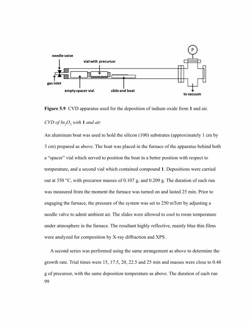
Figure 5.9 CVD apparatus used for the deposition of indium oxide from 1 and air.
CVD of In2O3 with 1 and air
An aluminum boat was used to hold the silicon (100) substrates (approximately 1 cm by
3 cm) prepared as above. The boat was placed in the furnace of the apparatus behind both
a “spacer” vial which served to position the boat in a better position with respect to
temperature, and a second vial which contained compound 1. Depositions were carried
out at 350 °C, with precursor masses of 0.107 g, and 0.209 g. The duration of each run
was measured from the moment the furnace was turned on and lasted 25 min. Prior to
engaging the furnace, the pressure of the system was set to 250 mTorr by adjusting a
needle valve to admit ambient air. The slides were allowed to cool to room temperature
under atmosphere in the furnace. The resultant highly reflective, mainly blue thin films
were analyzed for composition by X-ray diffraction and XPS .
A second series was performed using the same arrangement as above to determine the
growth rate. Trial times were 15, 17.5, 20, 22.5 and 25 min and masses were close to 0.48
g of precursor, with the same deposition temperature as above. The duration of each run
99
was measured from the moment the furnace was turned on and ended with the immediate
removal of the slide from the furnace. The slide was then allowed to cool on the benchtop
under atmosphere.
A third deposition was performed using the arrangement above to determine the
crystallinity of the film at lower deposition temperature. The trial time was 15 min and
the mass of 1 was 0.479g. The deposition temperature was 300 °C and the duration of the
run was measured from the moment the furnace was turned on and ended with the
immediate removal of the slide from the furnace. The slide was then allowed to cool on
the benchtop under atmosphere.
5.6 Conclusions
In[(NiPr)2CNMe2]3 (1) was easy to synthesize, recrystallize, and sublime with
excellent yields. Although it was stable to sublimation at 150 °C at 85 mTorr, it was
found to eliminate protonated guanidine when sitting in an inert atmosphere for extended
periods of time. Additionally, it was found to produce diisopropylcarbodiimide and
dimethylamine when heated to 140 °C as a solution in deuterated benzene.
Thermogravimetric analyses suggested that 1 decomposed to indium metal in an inert
atmosphere, and this was corroborated by vacuum CVD experiments without a reactant
gas at temperatures above 275 °C.
100
When air was used as a reactant gas in a CVD experiment above 275 °C, the
compound was found to produce transparent indium oxide. When 325 °C was used, the
films were found to be crystalline, cubic indium oxide, and occasionally had a small
impurity of indium metal. This suggests a film growth mechanism where indium
undergoes reduction and is then re-oxidized to In2O3.
101
Chapter 6 - Metallic Silver and Gold Chemical Vapour Deposition from
Novel Precursors
Results presented below have been submitted in a separate, original manuscript to Chem. Mater. in July 2013 as:
“Thermally Robust Gold and Silver Iminopyrrolidinates for Chemical Vapour Deposition of Metal Films”
Jason P. Coyle1*, Peter G. Gordon1, Adam P. Wells1, Eric R. Sirianni2, Glenn P. A. Yap2, Seán T. Barry1
1 Department of Chemistry, Carleton University, 1125 Colonel By Drive, Ottawa, K1S 5B6, Canada2 Department of Chemistry & Biochemistry, University of Delaware, Newark, Delaware 19716, USA
6.1 Abstract
Dimeric silver(I) and gold(I) tert-butyl-imino-2,2-dimethylpyrrolidinates were
synthesized and evaluated for thermal stability by thermal gravimetric analysis (TGA),
differential scanning calorimetry (DSC) and variable-temperature solution NMR.
Subsequently these compounds were used to deposit metallic films on silicon and glass
substrates by chemical vapour deposition (CVD), with and without a flow of heated
nitrogen gas. A previously reported analogous copper(I) compound with excellent
thermal properties motivated this investigation and is used for comparison. The present
compounds decomposed to produce metallic films at 140 °C for the silver compound and
300 °C for the gold compound in CVD experiments under roughing pump vacuum.
Additional CVD experiments with heated nitrogen gas flow improved film uniformity
102
without sacrificing film purity. The deposition and characterization of metallic silver and
gold films from these precursors is reported here.
6.2 Introduction
Longstanding research interest regarding the preparation of thin metallic films of Cu,
Ag, and Au has been rapidly increasing over the past few decades. Each of these metals
possess extremely low resistivities (and gold is highly resistant to corrosion) and so these
elements are often employed as interconnects in microelectronics. Plasmonic effects,
particularly the surface plasmons of these coinage metals121 are well known and research
into their implementation in photonic devices is rapidly increasing.122 As electronic
devices shrink, so to do their circuits. Processes that can create metallic architectures with
decreasing feature size and increasing precision are required to move forward. Chemical
vapour deposition123 (CVD) and atomic layer deposition42 (ALD) for thin film deposition
are becoming routine in industry for a wide variety of materials as they are ideal
technologies for coating geometrically complex substrates with high aspect ratio
features.124 An understanding of the thermal behaviour of the precursors used to create
these thin films is required for precise process control and innovation in precursor design.
Many examples of Cu(I) and Cu(II) homoleptic compounds have been reported for
both ALD and CVD copper thin film processes including β-diketonates,125,126 β-
diketiminates,127 amidinates,128–131 guanidinates,132 aminoalkoxides133 and
103
pyrrolylaldiminates.134 Reports of homoleptic precursors for silver and gold are less
common, which may be attributed at least in part to the larger ionic radii of silver and
gold compared to copper. As there is more space for coordination, non-volatile oligomers
or polymers of silver(I) and gold(I) are often obtained, frustrating the search for
appropriate gas-phase precursors.135 Perhaps mainly due to cost concerns, industry tends
to select for copper precursors for interconnects in microchip fabrication whereas silver
and gold thin films have remained primarily an academic pursuit. This may change, as
recently a previously known CVD precursor for silver films has been re-investigated and
employed as a plasma enhanced-ALD precursor136 for use in surface-enhanced Raman
spectroscopy (SERS) applications.137–140 Also, a gold guanidinate141 CVD precursor has
been used to coat fibre optics as part of a plasmonic device platform.142,39 The potential of
these applications may outweigh their cost.
There exist only a few reports in the literature of ligands for which a complete series
of copper, silver, and gold compounds have been prepared and their characteristics
compared.143–145 While copper amidinates are well-known precursors for ALD,128 silver
and gold amidinates volatilize and decompose within the same temperature range. Alkyl
substituted guanidinate compounds (Figure 6.1) have shown similar behaviour and have
been used as CVD precursors in custom built reactors.132,141
104
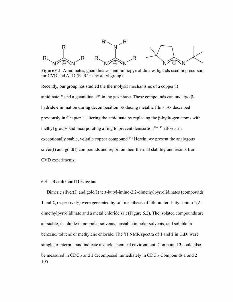
Figure 6.1 Amidinates, guanidinates, and iminopyrrolidinates ligands used in precursors for CVD and ALD (R, R’ = any alkyl group).
Recently, our group has studied the thermolysis mechanisms of a copper(I)
amidinate146 and a guanidinate116 in the gas phase. These compounds can undergo β-
hydride elimination during decomposition producing metallic films. As described
previously in Chapter 1, altering the amidinate by replacing the β-hydrogen atoms with
methyl groups and incorporating a ring to prevent deinsertion116,147 affords an
exceptionally stable, volatile copper compound.148 Herein, we present the analogous
silver(I) and gold(I) compounds and report on their thermal stability and results from
CVD experiments.
6.3 Results and Discussion
Dimeric silver(I) and gold(I) tert-butyl-imino-2,2-dimethylpyrrolidinates (compounds
1 and 2, respectively) were generated by salt metathesis of lithium tert-butyl-imino-2,2-
dimethylpyrrolidinate and a metal chloride salt (Figure 6.2). The isolated compounds are
air stable, insoluble in nonpolar solvents, unstable in polar solvents, and soluble in
benzene, toluene or methylene chloride. The 1H NMR spectra of 1 and 2 in C6D6 were
simple to interpret and indicate a single chemical environment. Compound 2 could also
be measured in CDCl3 and 1 decomposed immediately in CDCl3. Compounds 1 and 2 105
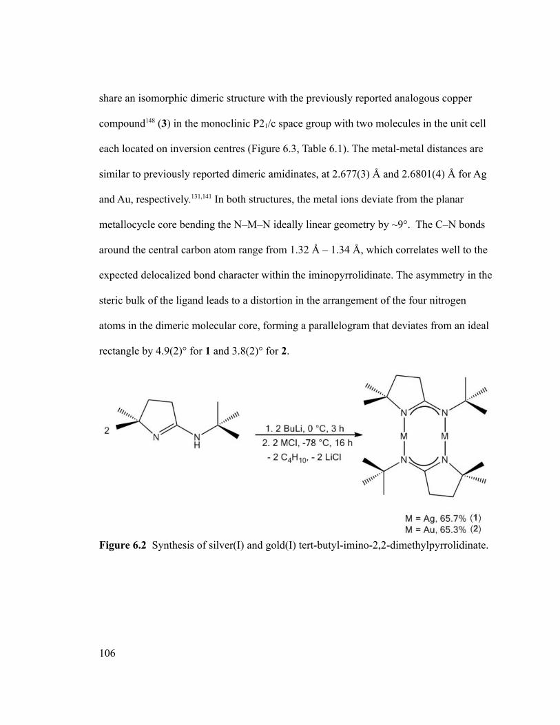
share an isomorphic dimeric structure with the previously reported analogous copper
compound148 (3) in the monoclinic P21/c space group with two molecules in the unit cell
each located on inversion centres (Figure 6.3, Table 6.1). The metal-metal distances are
similar to previously reported dimeric amidinates, at 2.677(3) Å and 2.6801(4) Å for Ag
and Au, respectively.131,141 In both structures, the metal ions deviate from the planar
metallocycle core bending the N–M–N ideally linear geometry by ~9°. The C–N bonds
around the central carbon atom range from 1.32 Å – 1.34 Å, which correlates well to the
expected delocalized bond character within the iminopyrrolidinate. The asymmetry in the
steric bulk of the ligand leads to a distortion in the arrangement of the four nitrogen
atoms in the dimeric molecular core, forming a parallelogram that deviates from an ideal
rectangle by 4.9(2)° for 1 and 3.8(2)° for 2.
Figure 6.2 Synthesis of silver(I) and gold(I) tert-butyl-imino-2,2-dimethylpyrrolidinate.
106
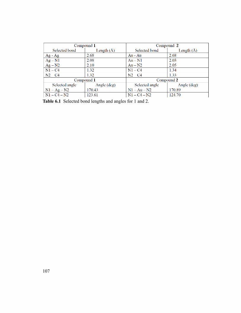
Table 6.1 Selected bond lengths and angles for 1 and 2.
107
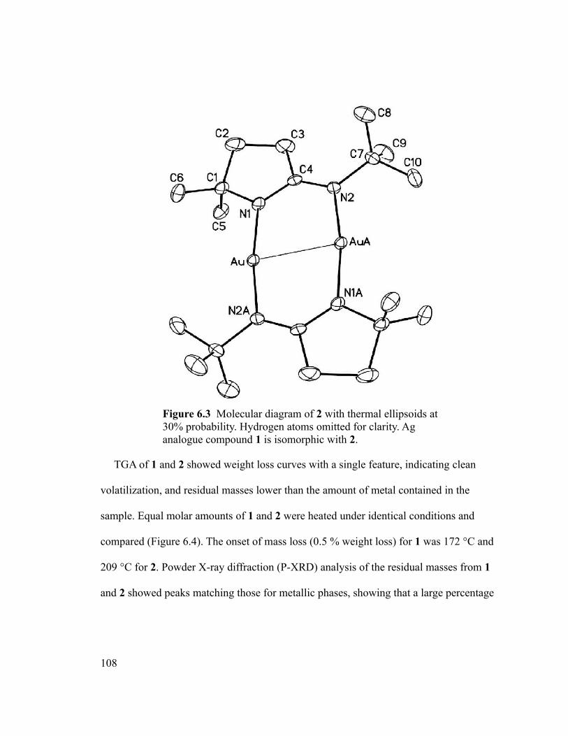
Figure 6.3 Molecular diagram of 2 with thermal ellipsoids at 30% probability. Hydrogen atoms omitted for clarity. Ag analogue compound 1 is isomorphic with 2.
TGA of 1 and 2 showed weight loss curves with a single feature, indicating clean
volatilization, and residual masses lower than the amount of metal contained in the
sample. Equal molar amounts of 1 and 2 were heated under identical conditions and
compared (Figure 6.4). The onset of mass loss (0.5 % weight loss) for 1 was 172 °C and
209 °C for 2. Powder X-ray diffraction (P-XRD) analysis of the residual masses from 1
and 2 showed peaks matching those for metallic phases, showing that a large percentage
108
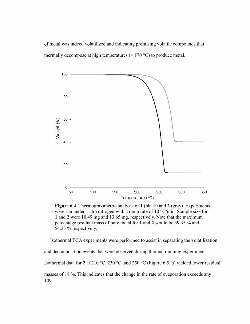
of metal was indeed volatilized and indicating promising volatile compounds that
thermally decompose at high temperatures (> 170 °C) to produce metal.
Figure 6.4 Thermogravimetric analysis of 1 (black) and 2 (gray). Experiments were run under 1 atm nitrogen with a ramp rate of 10 °C/min. Sample size for 1 and 2 were 10.49 mg and 13.65 mg, respectively. Note that the maximum percentage residual mass of pure metal for 1 and 2 would be 39.35 % and 54.23 % respectively.
Isothermal TGA experiments were performed to assist in separating the volatilization
and decomposition events that were observed during thermal ramping experiments.
Isothermal data for 2 at 210 °C, 230 °C, and 250 °C (Figure 6.5, b) yielded lower residual
masses of 18 %. This indicates that the change in the rate of evaporation exceeds any 109
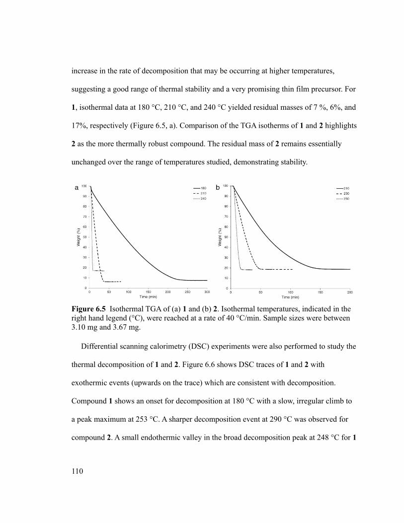
increase in the rate of decomposition that may be occurring at higher temperatures,
suggesting a good range of thermal stability and a very promising thin film precursor. For
1, isothermal data at 180 °C, 210 °C, and 240 °C yielded residual masses of 7 %, 6%, and
17%, respectively (Figure 6.5, a). Comparison of the TGA isotherms of 1 and 2 highlights
2 as the more thermally robust compound. The residual mass of 2 remains essentially
unchanged over the range of temperatures studied, demonstrating stability.
Figure 6.5 Isothermal TGA of (a) 1 and (b) 2. Isothermal temperatures, indicated in the right hand legend (°C), were reached at a rate of 40 °C/min. Sample sizes were between 3.10 mg and 3.67 mg.
Differential scanning calorimetry (DSC) experiments were also performed to study the
thermal decomposition of 1 and 2. Figure 6.6 shows DSC traces of 1 and 2 with
exothermic events (upwards on the trace) which are consistent with decomposition.
Compound 1 shows an onset for decomposition at 180 °C with a slow, irregular climb to
a peak maximum at 253 °C. A sharper decomposition event at 290 °C was observed for
compound 2. A small endothermic valley in the broad decomposition peak at 248 °C for 1
110
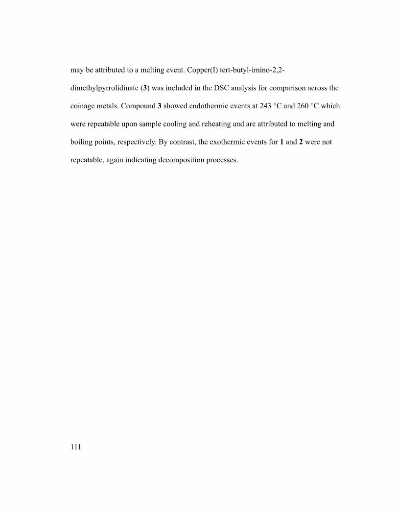
may be attributed to a melting event. Copper(I) tert-butyl-imino-2,2-
dimethylpyrrolidinate (3) was included in the DSC analysis for comparison across the
coinage metals. Compound 3 showed endothermic events at 243 °C and 260 °C which
were repeatable upon sample cooling and reheating and are attributed to melting and
boiling points, respectively. By contrast, the exothermic events for 1 and 2 were not
repeatable, again indicating decomposition processes.
111
Figure 6.6 Differential scanning calorimetry of 1, 2, and 3 in hermetically sealed aluminum pans. Temperature ramp was 10 °C/min up to 325 °C. Sample masses were 1.066 mg, 1.625 mg, and 3.790 mg for 1, 2, and 3, respectively. Exotherms are up.
The evaporation kinetics of 1 and 2 were evaluated by stepped isothermal TGA
between 130 °C – 190 °C (Figure 6.7). Lower temperatures were evaluated as this
minimizes mass loss due to decomposition. Both compounds presented evaporation rates
with Arrhenius temperature dependence. The expected higher rates of evaporation for
compounds of lower molecular mass (as compared to 3) was observed. While
112
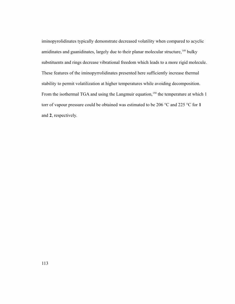
iminopyrolidinates typically demonstrate decreased volatility when compared to acyclic
amidinates and guanidinates, largely due to their planar molecular structure,149 bulky
substituents and rings decrease vibrational freedom which leads to a more rigid molecule.
These features of the iminopyrrolidinates presented here sufficiently increase thermal
stability to permit volatilization at higher temperatures while avoiding decomposition.
From the isothermal TGA and using the Langmuir equation,150 the temperature at which 1
torr of vapour pressure could be obtained was estimated to be 206 °C and 225 °C for 1
and 2, respectively.
113
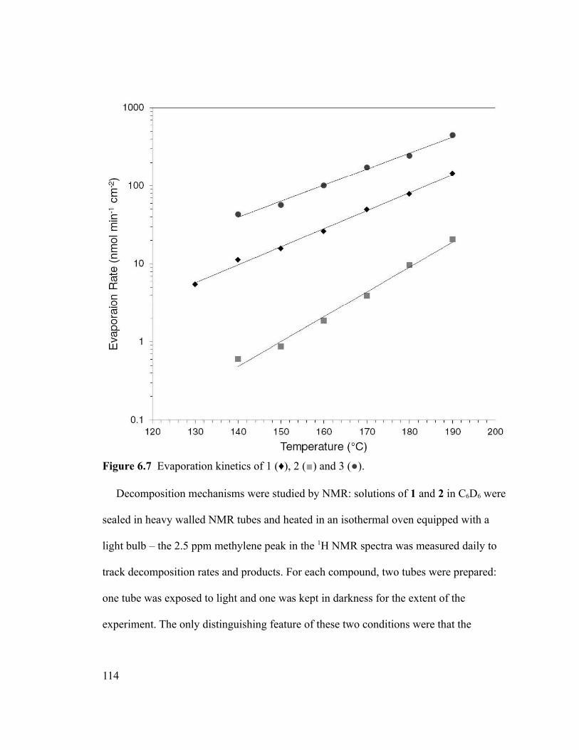
Figure 6.7 Evaporation kinetics of 1 (♦), 2 (■) and 3 (●).
Decomposition mechanisms were studied by NMR: solutions of 1 and 2 in C6D6 were
sealed in heavy walled NMR tubes and heated in an isothermal oven equipped with a
light bulb – the 2.5 ppm methylene peak in the 1H NMR spectra was measured daily to
track decomposition rates and products. For each compound, two tubes were prepared:
one tube was exposed to light and one was kept in darkness for the extent of the
experiment. The only distinguishing feature of these two conditions were that the
114
solutions exposed to light completely decomposed in less time, which was most apparent
near the end of the experiments. Under both light and dark conditions, compound 2
decomposed at 100 °C whereas 1 showed negligible decomposition at 100 °C and instead
required a temperature of 120 °C to decompose within the same time frame as 2 (Figure
6.8). The decomposition of both compounds resulted in a metallic mirror plating out on
the tube walls. A rate order could not be assigned unambiguously to any of the
decomposition trends as each trend showed similar fits to zero, 1st and 2nd order plots.
This ambiguity in rate analysis suggests a complex decomposition mechanism which may
involve both surface and solution based reactions. Interestingly, protonated ligand was
the only decomposition product observed by 1H NMR for each experiment.
115
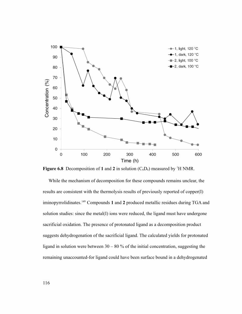
Figure 6.8 Decomposition of 1 and 2 in solution (C6D6) measured by 1H NMR.
While the mechanism of decomposition for these compounds remains unclear, the
results are consistent with the thermolysis results of previously reported of copper(I)
iminopyrrolidinates.149 Compounds 1 and 2 produced metallic residues during TGA and
solution studies: since the metal(I) ions were reduced, the ligand must have undergone
sacrificial oxidation. The presence of protonated ligand as a decomposition product
suggests dehydrogenation of the sacrificial ligand. The calculated yields for protonated
ligand in solution were between 30 – 80 % of the initial concentration, suggesting the
remaining unaccounted-for ligand could have been surface bound in a dehydrogenated
116
state. Similar chemistry has been proposed for the surface decomposition of copper(I)
amidinates, guanidinates, and iminopyrrolidinates.151,152
The promising results from these thermolysis studies prompted an investigation of
these compounds as CVD precursors for metallic films. CVD experiments were carried
out in a tube furnace reactor on SiO2 and Si substrates (Figure 6.15). The first series of
depositions were carried out under roughing pump vacuum conditions. The second set
were carried out with a flow of heated nitrogen gas to assist in mass transport.
Independent heating zones were employed for the nitrogen, precursor bubbler, and
furnace areas.
Depositions Without Nitrogen Flow
For 1, the bubbler was heated to 110 °C and maintained for 3h at 35 mtorr.
Approximately 50 to 60 mg of 1 in an open glass vial was completely volatilized under
these conditions for each deposition. The onset for film deposition was found to be 140
°C which afforded films less than 5 nm thick, as measured by AFM. Increasing the
substrate temperature in 20 °C increments from 140 °C to 220 °C afforded increasingly
thicker films each with a thickness gradient receding from the precursor inlet (Figure 6.9,
bottom). This series of depositions demonstrates 1 to be stable in the gas phase and at the
substrate surface below 140 °C while 1 is completely consumed in the tube furnace above
temperatures of 200 °C. The deposited films were confirmed to be metallic silver by
XRD and a 156 nm thick film deposited at 220 °C on SiO2 had a sheet resistance of
117
0.0158 Ω/ٱ. Images obtained by scanning electron microscopy (SEM) showed the silver
films deposited at 200 °C to be granular with particle sizes corresponding to film
thickness (Figure 6.10; a, b). The films were further confirmed to be metallic silver by
XPS and EDX analysis.
Compound 2 was tested in a similar manner as a precursor for CVD of gold films on
Si substrates. Approximately 30 mg of 2 was heated in a bubbler vial to 130 °C over a 16
h deposition at 35 mtorr. Upon inspection of the vial it was observed that the mass of
precursor was not entirely consumed; however, the material remaining consisted of
completely intact precursor as determined by 1H NMR analysis. The onset of film
deposition was found to be 300 °C. Increasing the tube furnace temperature in 50 °C
increments from 300 °C to 500 °C afforded a thickness profile with a thickness maximum
that migrated towards the precursor inlet at higher temperatures (Figure 6.9, top). The
thickness profile observed for 2 was significantly different than 1 and this can be
attributed at least in part to a more pronounced temperature gradient across the tube
furnace at higher temperatures. This series of depositions demonstrates 2 to be stable in
the gas phase and at the substrate’s surface below 300 °C. Film thickness at the centre of
the tube furnace reached a maximum at a temperature of 350 °C and deposition occurred
predominately at the precursor inlet at a temperature of 500 °C. The deposited films were
confirmed to be metallic gold by XRD. Images obtained by SEM of the gold films
deposited at 350 °C consisted of densely packed particles of < 50 nm (Figure 6.10; c, d).
Interestingly, film thickness did not correspond to particle size and the thicker areas
118
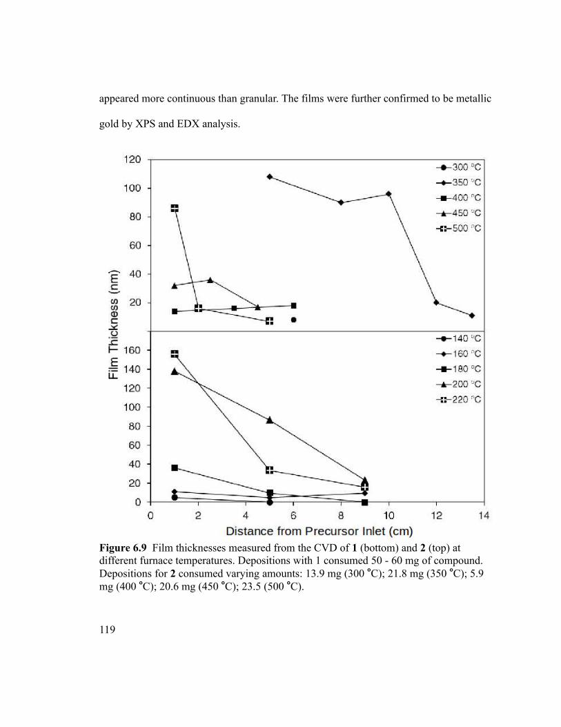
appeared more continuous than granular. The films were further confirmed to be metallic
gold by XPS and EDX analysis.
Figure 6.9 Film thicknesses measured from the CVD of 1 (bottom) and 2 (top) at different furnace temperatures. Depositions with 1 consumed 50 - 60 mg of compound. Depositions for 2 consumed varying amounts: 13.9 mg (300 °C); 21.8 mg (350 °C); 5.9 mg (400 °C); 20.6 mg (450 °C); 23.5 (500 °C).
119
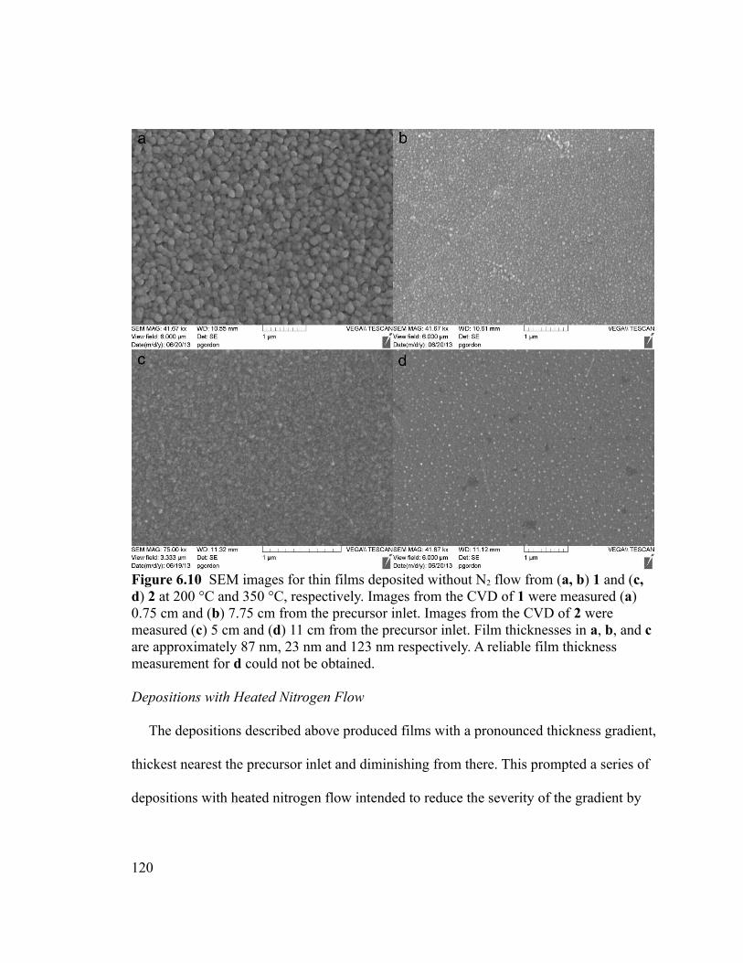
Figure 6.10 SEM images for thin films deposited without N2 flow from (a, b) 1 and (c, d) 2 at 200 °C and 350 °C, respectively. Images from the CVD of 1 were measured (a) 0.75 cm and (b) 7.75 cm from the precursor inlet. Images from the CVD of 2 were measured (c) 5 cm and (d) 11 cm from the precursor inlet. Film thicknesses in a, b, and c are approximately 87 nm, 23 nm and 123 nm respectively. A reliable film thickness measurement for d could not be obtained.
Depositions with Heated Nitrogen Flow
The depositions described above produced films with a pronounced thickness gradient,
thickest nearest the precursor inlet and diminishing from there. This prompted a series of
depositions with heated nitrogen flow intended to reduce the severity of the gradient by
120
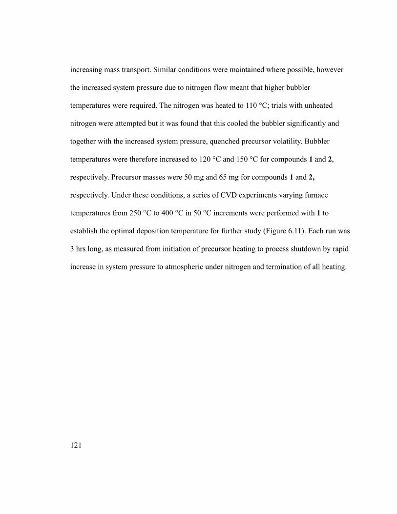
increasing mass transport. Similar conditions were maintained where possible, however
the increased system pressure due to nitrogen flow meant that higher bubbler
temperatures were required. The nitrogen was heated to 110 °C; trials with unheated
nitrogen were attempted but it was found that this cooled the bubbler significantly and
together with the increased system pressure, quenched precursor volatility. Bubbler
temperatures were therefore increased to 120 °C and 150 °C for compounds 1 and 2,
respectively. Precursor masses were 50 mg and 65 mg for compounds 1 and 2,
respectively. Under these conditions, a series of CVD experiments varying furnace
temperatures from 250 °C to 400 °C in 50 °C increments were performed with 1 to
establish the optimal deposition temperature for further study (Figure 6.11). Each run was
3 hrs long, as measured from initiation of precursor heating to process shutdown by rapid
increase in system pressure to atmospheric under nitrogen and termination of all heating.
121
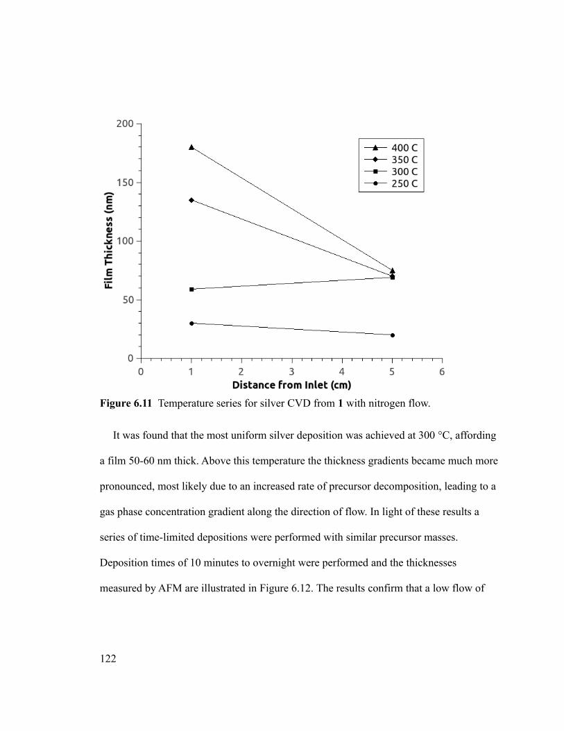
Figure 6.11 Temperature series for silver CVD from 1 with nitrogen flow.
It was found that the most uniform silver deposition was achieved at 300 °C, affording
a film 50-60 nm thick. Above this temperature the thickness gradients became much more
pronounced, most likely due to an increased rate of precursor decomposition, leading to a
gas phase concentration gradient along the direction of flow. In light of these results a
series of time-limited depositions were performed with similar precursor masses.
Deposition times of 10 minutes to overnight were performed and the thicknesses
measured by AFM are illustrated in Figure 6.12. The results confirm that a low flow of
122
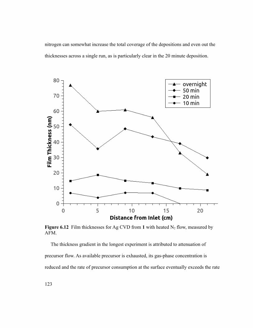
nitrogen can somewhat increase the total coverage of the depositions and even out the
thicknesses across a single run, as is particularly clear in the 20 minute deposition.
Figure 6.12 Film thicknesses for Ag CVD from 1 with heated N2 flow, measured by AFM.
The thickness gradient in the longest experiment is attributed to attenuation of
precursor flow. As available precursor is exhausted, its gas-phase concentration is
reduced and the rate of precursor consumption at the surface eventually exceeds the rate
123
of mass transport along the surface. Therefore the deposition zone slowly moves back
towards the source as precursor is depleted, generating a thicker film closer to the inlet.
Figure 6.13 presents data that confirms agreement between AFM and SEM analysis of
film thickness. AFM was used exclusively for the remainder of film measurements as
sample preparation was straightforward and analysis more economical.
Figure 6.13 Thickness profile for Ag CVD at 300 °C, with nitrogen flow, comparing values obtained by SEM and AFM.
Nearly identical CVD experiments under flow of nitrogen were performed with 2. It
was found that the flow had a much less pronounced effect on film thicknesses (Figure
124
6.14), particularly at 300 °C which demonstrated no significant change. Intermediate
temperatures of 350 °C and 400 °C resulted in intermediate thicknesses, demonstrating
growth similar to the curve observed for 450 °C.. The large decrease in thickness past 12
cm for the higher temperatures suggests rapid film growth is depleting the precursor
before it can reach more distant areas. The relatively flat films deposited at 300 °C
indicate very even, slow decomposition at the surface. This stability is a promising result
for the use of 2 as a CVD precursor, and suggests that it should be evaluated as an ALD
precursor as well.
125
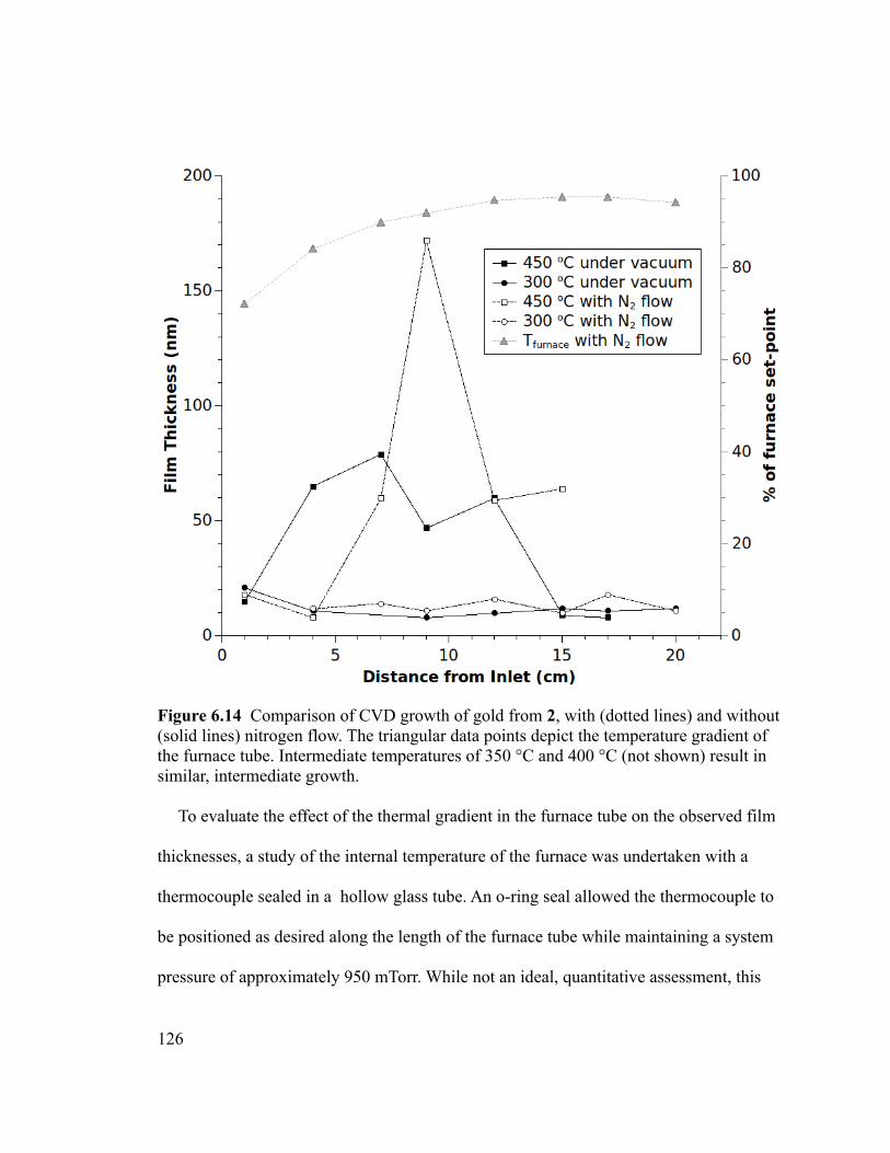
Figure 6.14 Comparison of CVD growth of gold from 2, with (dotted lines) and without (solid lines) nitrogen flow. The triangular data points depict the temperature gradient of the furnace tube. Intermediate temperatures of 350 °C and 400 °C (not shown) result in similar, intermediate growth.
To evaluate the effect of the thermal gradient in the furnace tube on the observed film
thicknesses, a study of the internal temperature of the furnace was undertaken with a
thermocouple sealed in a hollow glass tube. An o-ring seal allowed the thermocouple to
be positioned as desired along the length of the furnace tube while maintaining a system
pressure of approximately 950 mTorr. While not an ideal, quantitative assessment, this
126
allowed for a rough estimate of the temperature gradient experienced by the substrates.
For a furnace set-point of 400 °C, allowed to equilibrate for 3 hrs, the gradient began at 1
cm from the precursor inlet at 72% of the furnace set-point value and approached 95% of
the value by the midpoint of the furnace, about 15 cm from the precursor inlet (Figure
6.14). At 20 cm the temperature gently curved back down to 68% by 29 cm. Further
equilibration time did not significantly alter these values. Variations in film thickness can
in part be attributed to this thermal gradient, but the effect of film growth rate must also
be considered. The growth rate at 450 °C under nitrogen peaks at 9 cm, but this does not
imply that higher temperatures downstream of this point are not amendable to growth; it
is more likely that around this temperature growth rate is so rapid as to consume
precursor faster than it can be delivered, and so growth downstream is frustrated by lack
of precursor.
A study of precursor mass consumption was beyond the scope of this work but would
provide valuable insight into the nature of the deposition. A series of experiments that
varied precursor mass load of 1 and 2 for a fixed deposition duration and temperature
could provide very useful data.
6.4 Experimental
General Considerations
Some manipulations (loading, filtering, and isolation) were performed in an MBraun
Labmaster™ 130 Dry box (mBraun, Stratham, NH, U.S.A.) under a nitrogen atmosphere
127
while additions were performed by standard Schlenk techniques. NMR spectra were
recorded on a 400 MHz Bruker AMX spectrometer. NMR spectra were measured in C6D6
or CDCl3 and were referenced against residual protonated solvent or TMS, respectively.
Tert-butylimino-2,2-dimethylpyrrolidine40 and THT·AuCl153 were prepared according to
literature. AgCl was purchased from Strem Chemicals and used as received. Canadian
Microanalytical Service Ltd. performed combustion analysis. Thermogravimetric analysis
was performed on a TA Instruments Q50 apparatus located in an MBraun Labmaster130
Dry box under a nitrogen atmosphere. Differential scanning calorimetry was performed
on a DSC Instruments Q10 apparatus. Toluene and diethyl ether were purchased as ACS
grade and purified from an Mbraun Solvent Purifier System. Dichloromethane and
pentane were purchased as anhydrous from Sigma Aldrich Chemical Company and used
as received
Silver(I) tert-butyl-imino-2,2-dimethylpyrrolidinate (1): Tert-butyl-imino-2,2-
dimethylpyrrolidine (3.364 g, 20.0 mmol) was dissolved in 60 mL of toluene and cooled
to 0 °C. Butyl lithium in hexanes (2.5 M, 8.0 mL, 20.0 mmol) was added dropwise and
the solution was stirred for 3h at room temperature. In a separate 500 mL Schlenk flask
wrapped in aluminum foil, AgCl (2.865 g, 20.0 mmol) was suspended in 200 mL of
toluene. The lithiated iminopyrrolidinate solution was added dropwise via cannula over 1
h and the resulting mixture was stirred for 16 h. The reaction mixture was filtered and the
insoluble solids were washed with 20mL of toluene. Volatiles were stripped off from the
combined wash and filtrate to afford a light brown solid. The insoluble solids were
128
washed further with dichloromethane (3 x 20 mL). These washings were combined and
volatiles were stripped off to afford more of the light brown solid. The two portions of
solid were combined and washed with pentane (4 x 10 mL). The crude solid was
recrystallized from 20 mL of hot toluene in a pressure vessel to afford colourless, block
crystals; 3.615g, 65.7%. 1H NMR (400 MHz, C6D6): δ 1.16 (s, 6H, NC(CH3)2CH2CH2C),
δ 1.29 (s, 9H, NC(CH3)3, δ 1.65 (t, 2H, NC(CH3)2CH2CH2C), δ 2.54 (t, 2H,
NC(CH3)2CH2CH2C) 13C NMR (400 MHz, C6D6): 32.89 (NC(CH3)2CH2CH2C), 33.79
(NC(CH3)2CH2CH2C), 33.98 (NC(CH3)3), 38.26 (NC(CH3)2CH2CH2C), 52.81
(NC(CH3)2CH2CH2C), 61.29 (NC(CH3)3), 175.12 (NCN) Combustion analysis,
found(calculated): C, 43.21(43.65); H, 7.04(6.96); N, 10.15(10.18).
Gold(I) tert-butyl-imino-2,2-dimethylpyrrolidinate (2): Tert-butyl-imino-2,2-
dimethylpyrrolidine (2.874 g, 17.1 mmol) was dissolved in 60 mL of toluene and cooled
to 0 °C. Butyl lithium in hexanes (2.5 M, 6.83 mL, 17.1 mmol) was added dropwise and
the solution was stirred for 3h at room temperature. In a separate 500 mL Schlenk flask
wrapped in aluminum foil, THT·AuCl (5.475, 17.1 mmol) was suspended in 175mL of
toluene and cooled to -78 °C. The lithiated iminopyrrolidinate solution was added
dropwise via cannula over 1 h and the resulting mixture was stirred for 16 h gradually
warming to room temperature. Volatiles were stripped off under reduced pressure to
afford a dark solid which was dried under high-vac to remove residual THT. The solid
was stirred with warm toluene (4 x 50 mL) for 15 min and filtered. The extractions were
combined and volatiles were removed under reduced pressure to afford a solid that was
129
washed with diethyl ether (4 x 5 mL). The solid was dissolved in 20 mL of hot toluene in
a pressure vessel and left to stand for 12 h cooling to room temperature. A crop of
colourless, block crystals were isolated by decanting the supernatant, washing with
diethyl ether (3 x 5 mL) and dried under vacuum to afford 2.100 g. A second crop of
product was obtained from the insoluble solid that remained post toluene extraction. The
remaining insoluble solids were stirred with dichloromethane (4 x 50 mL) for 15 min and
filtered. The extractions were combined and volatiles were removed under reduced
pressure to afford a solid that was washed with diethyl ether (4 x 5 mL). The solid was
dissolved in 20 mL of hot toluene in a pressure vessel and left to stand for 12 h cooling to
room temperature. A second crop of colourless, block crystals were isolated by decanting
the supernatant, washing with diethyl ether (3 x 5 mL) and drying under vacuum to afford
1.960 g; total yield was 4.060 g, 65.3%. 1H NMR (400 MHz, CDCl3): δ 1.18 (s, 6H,
NC(CH3)2CH2CH2C), δ 1.38 (s, 9H, NC(CH3)3), δ 1.72 (t, 2H, NC(CH3)2CH2CH2C), δ
2.73 (t, 2H, NC(CH3)2CH2CH2C) 13C NMR (400 MHz, CDCl3): δ 30.48
(NC(CH3)2CH2CH2C), δ 33.69 (NC(CH3)3), δ 34.25 (NC(CH3)2CH2CH2C), δ 36.78
(NC(CH3)2CH2CH2C), δ 55.99 (NC(CH3)2CH2CH2C), δ 63.45 (NC(CH3)3), δ 176.47
(NCN) Combustion analysis, found(calculated): C, 32.85(32.98); H, 5.23(5.26); N,
7.67(7.69).
Crystal Structure studies for compounds 1 and 2: Crystals were selected, sectioned
as required, and mounted on plastic mesh with viscous oil and flash-cooled to the data
collection temperature. Diffraction data were collected on a Bruker-AXS APEX II Duo
130
CCD diffractometer with graphite-monochromated Mo-Kα radiation (λ=0.71073 Å). The
data-sets were treated with SADABS absorption corrections based on redundant
multiscan data. The unit cell parameters and systematic absences in the diffraction data
were uniquely consistent for P21/c. The isomorphic structures were solved using direct
methods and refined with full-matrix,least-squares procedures on F2. Unit cell parameters
were determined by sampling three different sections of the Ewald sphere. Nonhydrogen
atoms were refined with anisotropic displacement parameters. Hydrogen atoms were
treated as idealized contributions. Structure factors and anomalous dispersion coefficients
are contained in the SHELXTL 6.12 program library.120 The structures have been
deposited at the Cambridge Crystallographic Data Centre under CCDC 949353 &
949354.
Chemical Vapour Deposition
Depositions were conducted in a custom built CVD apparatus (Figure 6.15). A coil of
3 mm stainless steel tubing heated with resistive heating rope controlled by a variable
autotransformer was employed for heated nitrogen gas delivery. Nitrogen flow was
regulated with a needle valve to achieve the desired process pressure. The nitrogen was
delivered to a “bubbler” section 15 cm long containing the precursor and independently
heated with resistive heating tape. The bubbler was directly connected to the deposition
tube which was enclosed in a clamshell-type furnace approximately 50 cm long. The
substrates were placed in the centre of the furnace tube to minimize thermal gradients and
131
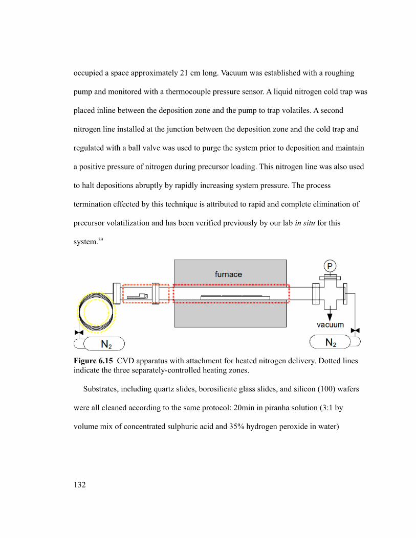
occupied a space approximately 21 cm long. Vacuum was established with a roughing
pump and monitored with a thermocouple pressure sensor. A liquid nitrogen cold trap was
placed inline between the deposition zone and the pump to trap volatiles. A second
nitrogen line installed at the junction between the deposition zone and the cold trap and
regulated with a ball valve was used to purge the system prior to deposition and maintain
a positive pressure of nitrogen during precursor loading. This nitrogen line was also used
to halt depositions abruptly by rapidly increasing system pressure. The process
termination effected by this technique is attributed to rapid and complete elimination of
precursor volatilization and has been verified previously by our lab in situ for this
system.39
Figure 6.15 CVD apparatus with attachment for heated nitrogen delivery. Dotted lines indicate the three separately-controlled heating zones.
Substrates, including quartz slides, borosilicate glass slides, and silicon (100) wafers
were all cleaned according to the same protocol: 20min in piranha solution (3:1 by
volume mix of concentrated sulphuric acid and 35% hydrogen peroxide in water)
132
followed by a distilled water rinse and then allowed to dry in air. Substrate were all at
most 1.4cm wide and between 3 and 7cm long.
In a typical deposition experiment, the precursor was weighed out into a vial under
nitrogen in a glove box. The vial was then placed in the bubbler, sealed, and transported
to the CVD apparatus. Prior to this the substrates were previously placed in position in
the centre of the furnace tube. The bubbler was attached while the apparatus was under a
flow of nitrogen. The system was then evacuated and heating of the nitrogen delivery line
and furnace begun. A 30min equilibration period was allowed before depositions were
attempted. At time zero, bubbler heating was initiated and heated nitrogen flow was
adjusted using the needle valve until a system pressure of 100mTorr was achieved. The
heating ramp for the bubbler was performed by manual adjustment of the voltage
delivered to the heating tape, monitored by thermocouple, and effected rapidly. The
temperature was monitored using external thermocouples throughout the depositions to
ensure stability and the voltage was adjusted as required to maintain the desired process
temperature.
Film Characterization
Film morphology and composition were determined by scanning electron microscopy
(SEM) and electron dispersive x-ray spectroscopy (EDS) using a Tescan Vega-II XMU
VPSEM equipped with an Inca EDS. Quantitative analysis was calibrated using a pure
copper sample.
133
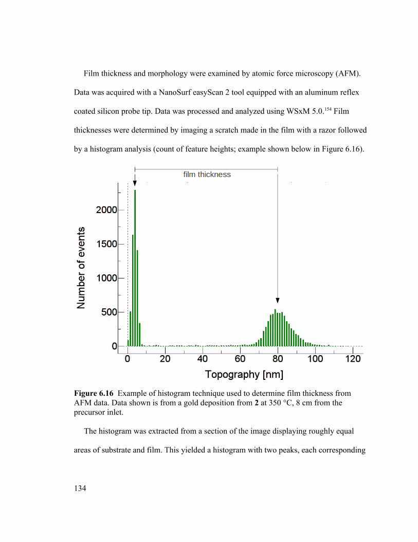
Film thickness and morphology were examined by atomic force microscopy (AFM).
Data was acquired with a NanoSurf easyScan 2 tool equipped with an aluminum reflex
coated silicon probe tip. Data was processed and analyzed using WSxM 5.0.154 Film
thicknesses were determined by imaging a scratch made in the film with a razor followed
by a histogram analysis (count of feature heights; example shown below in Figure 6.16).
Figure 6.16 Example of histogram technique used to determine film thickness from AFM data. Data shown is from a gold deposition from 2 at 350 °C, 8 cm from the precursor inlet.
The histogram was extracted from a section of the image displaying roughly equal
areas of substrate and film. This yielded a histogram with two peaks, each corresponding
134
to the most common heights of the substrate and the film respectively. The difference
between these two peaks was taken as the film thickness. This provides a reliable method
for thickness determination that also affords a qualitative examination of film roughness.
Film roughness was also quantitatively extracted from this data. A second technique was
employed to double-check film thickness characterization: the difference between
average heights taken from linear cross-sections of nearby film and substrate sections,
with generally good agreement. This method has shown good correlation with
thicknesses determined from SEM interrogation of cross-sections. Sheet resistance was
measured with a four-point probe.
Thermal Decomposition Solution Studies
Solutions of 1 and 2 were prepared by adding a known mass of compound to a known
mass of C6D6. A drop of TMS was added as an internal standard. The concentrations for 1
and 2 were 7.8 mM and 1.8 mM, respectively. The solutions were frozen in heavy walled
NMR tubes in liquid N2 and flamed sealed under 100 mtorr dynamic vacuum. The
isothermal oven was illuminated with a 60 W incandescent light bulb and NMR tubes
were wrapped with aluminum foil to exclude light. 1H NMR spectra were measured on a
300 MHz Avance 3 every 24 h after the tubes cooled to room temperature for 20 min.
6.5 Conclusion
Two thermally robust CVD precursors for silver and gold thin films were synthesized
and thermally characterized. Compounds 1 and 2 are thermally stable up to 170 °C as
135
pure solids. These precursors remained volatile up to 240 °C during TGA in 1 atm of
inert gas. Under low pressure CVD conditions, 1 and 2 could be volatilized, without
decomposition, between 110 °C – 130 °C. Under moderate flow of heated nitrogen
carrier gas, similar volatilization without decomposition was observed for 120 °C – 150
°C.
TGA, DSC and CVD experiments revealed 2 as more thermally stable than 1. The
trend in thermal stability for the series of coinage metal precursors was Cu > Au > Ag and
the trend in volatility was Cu > Ag > Au. In C6D6 solutions 1 was more thermally stable
than 2, where both compounds demonstrated increased decomposition rates under
exposure to light with otherwise identical conditions. Solution NMR thermal studies
resulted in metallic films on the tube surface and protonated ligand as the observable
decomposition products. Rates of decomposition in solution could not be fit to simple
models, suggesting complex decomposition pathways.
Compounds 1 and 2 are improved precursors for thermal CVD applications as
compared to other amidinate and guanidinate compounds – their evaporation temperature
and gas phase decomposition temperatures are well separated which is desirable for both
CVD and ALD. The ligand design successfully blocked the previously problematic low
temperature decomposition pathways of β-hydrogen abstraction and CDI de-
insertion.116 Thermal decomposition of 1 and 2 could still be achieved at reasonable CVD
process temperatures, affording metallic residues and thin films. The evidence suggests
dehydrogenation of the ligand at higher temperatures but a thorough gas phase
136
decomposition mechanism study will be required for a detailed understanding of the
process. Metallic thin films of silver and gold consisting of granular, nanoparticulate
films were deposited at low pressures between 140 °C - 220 °C and 300 °C - 500 °C,
respectively. Similar films were obtained from depositions with heated N2 flow at 250 °C
- 400 °C and 300 °C - 450 °C, respectively. Nitrogen flow assisted in greater film
thickness uniformity for depositions with 1 but no significant change was observed for
depositions with 2. Further work to fully characterize the composition of the films may
provide interesting insight into the deposition chemistry at the surface. Current
investigations are focusing on further optimization of CVD conditions, plasmonic device
fabrication, and evaluating the precursors in conjunction with reducing agents for use in
ALD processes.
137
Chapter 7 - Conclusions
While the individual projects described in this work are diverse, they all concern the
study and practical application of thin film deposition chemistry: the chemistry of the
precursors used for chemical vapour deposition and atomic layer deposition, and the
mechanism of thin film growth by these methods. Characterization of thin film
precursors, in particular studies of their thermal behaviour, was pursued not only to
evaluate the precursors for use in film deposition but also to examine their decomposition
pathways. The deposited films were evaluated by several criteria: physical and chemical
protection of metal alloys, optical and electronic behaviour, and physical morphology.
Bronze and brass coins and tokens were coated by ALD with aluminum oxide using a
previously reported process and were found to provide significant protection against
moderate chemical attack. Growth rates for deposition of films with thicknesses on the
order of 1000 – 10,000 Å were independent of substrate and it was found that the films
adhered more strongly to the metal substrates than to the silicon. This became particularly
pronounced at film thicknesses of 6000 Å and above, where the silicon substrates
demonstrated significant delamination. It was found that the TTIP/water ALD process
yielded good titanium oxide film growth on metal samples coated with 1200 Å of
aluminum oxide, as confirmed by XPS. The same process resulted in extremely poor
growth on uncoated metal samples. Uniformity experiments on batch depositions on 2744
substrates revealed that a pulse program with three subsets of precursor/purge pulses for
138
each precursor was required at a process temperature of 250 °C. A preliminary three hour
thermal equilibration period was also required for uniformity across all samples.
A study the effect of aluminum oxide thickness on perceived colour of the metal
substrates was performed. In addition to a 1200 Å film that induced no noticeable change
in colour, an array of colours including iridescence that may prove useful for numismatic,
limited edition coins were observed. The optical properties of thin films on metals and
metal alloys merit future investigation as anti-counterfeiting measures. Additionally, a
study of the nature and composition of the interface layer between metal substrates and
alumina film would help to understand both protective and cosmetic issues. A thorough
study of protection from wear and chemical attack, particularly using laminate films, is
recommended.
Motivated by these preliminary colour studies, a robot-based gonioreflectometer was
used to more carefully analyze the colours resulting from thin films (0 - 1613 Å) of
aluminum oxide deposited by ALD on silicon. The experimental reflectivities obtained
were compared to those predicted by software simulations and the observations were
found to deviate from simulated results along the metrics of film thickness, wavelength of
light, and angle of incidence/observation. With respect to film thickness, the largest
disagreement between theory and experiment was observed for the films near 800 Å.
These films are also the most iridescent. With respect to wavelength, the largest
disagreement was most often observed at short wavelengths, with 7 of the 12 samples
139
exhibiting their largest deviations from the model between the wavelengths of 380 and
445 nm. An angular analysis of the data showed that the disagreements were higher at
near-normal angles of reflection (≤15°). Future efforts towards a more accurate
simulation of the system should include measurements of the dispersion curves of the
deposited films. A comparison study with other film and substrate compositions should
also reveal interesting phenomena.
Various thicknesses of alumina films (approximately 4-10 nm) were deposited by ALD
on flat and nanostructured silicon substrates, and incorporated into architectures that were
then evaluated as photovoltaic devices. It was found that good photovoltaic MIS devices
are possible when a traditional metal is replaced with PEDOT. The reverse saturation
currents observed on flat devices made with Al2O3 films were quite similar to similar
devices made with an SiO2 layer. The forward currents are, however, substantially lower
for the devices with Al2O3. The structured samples with Al2O3 showed a considerable
increase in efficiency (of up to five times) over the equivalent flat samples.
The nanostructured silicon used in this work had aspect ratios of 1:1. To achieve
higher aspect ratio structures other techniques can be used such has etch of gold
deposited by CVD and self-masking electron cyclotron resonance reactive ion etching
(ECR RIE).34,155 The testing of the devices made with these techniques is ongoing.
It is expected that spin coating of PEDOT:PSS will be incompatible with the high
aspect ratio structures that we hope to use on the substrates in the future. To mitigate this
140
problem deposition of PEDOT by vapour phase polymerization (VPP) or In2O3 by CVD
will be attempted. The assembly of the deposition system is in progress.
The simple synthesis of a new indium precursor, In[(NiPr)2CNMe2]3, in high yields led
to promising CVD experiments of indium oxide films. The precursor was found to
eliminate protonated guanidine over time in an inert atmosphere, as well as producing
diisopropylcarbodiimide and dimethylamine when heated to 140 °C as a solution in
deuterated benzene. Thermogravimetric analyses suggested that 1 decomposed to indium
metal in an inert atmosphere, corroborated by vacuum CVD experiments without a
reactant gas at temperatures above 275 °C. When air was used as a reactant gas in a CVD
experiment above 275 °C, the compound was found to produce transparent indium oxide.
At a temperature of 325 °C, the films were found to be crystalline cubic indium oxide.
Small impurities of indium metal were observed, suggesting a film growth mechanism
where indium undergoes reduction and is then re-oxidized to In2O3. Further study of this
precursor for CVD or ALD deposition of indium metal is advised.
Two thermally robust CVD precursors for silver and gold thin films were synthesized
and thermally characterized. These precursors remained volatile up to 240 °C during
TGA in 1 atm of inert gas. Under low and high pressure CVD conditions, volatilization
without decomposition between 110 °C – 150 °C yielded metallic films of silver and gold
141
at deposition temperatures between 140 °C – 220 °C and 300 °C – 500 °C, respectively.
These films consisted of granular, nanoparticulate films on glass and silicon substrates.
Similar films were obtained from depositions with heated N2 flow at 250 °C - 400 °C and
300 °C - 450 °C, respectively. While nitrogen flow assisted in greater film thickness
uniformity for depositions with 1, no significant change was observed for depositions
with 2. Depositions with 2 at 300 °C yielded extremely uniform film thicknesses,
suggesting 2 may be useful as an ALD precursor.
TGA, DSC and CVD experiments revealed 2 as more thermally stable than 1. Solution
NMR thermal studies resulted in metallic films on the tube surface and protonated ligand
as the observable decomposition products. Rates of decomposition in solution could not
be fit to simple models, suggesting complex decomposition pathways. Further study will
be required to understand these solution-phase decomposition mechanisms. Thermal
characterization further revealed that the ligand design successfully blocked β-hydrogen
abstraction and CDI de-insertion decomposition pathways observed previously in
analogous amidinate and guanidinate compounds.98 The evidence suggests
dehydrogenation of the ligand at higher temperatures.
Current investigations are focusing on further optimization of CVD conditions,
plasmonic device fabrication, and evaluating the precursors in conjunction with reducing
agents for use in ALD processes. A thorough gas phase decomposition mechanism study
will also be required for a detailed understanding of the film deposition process.
142
References
1. L. Niinistö, M. Nieminen, J. Päiväsaari, J. Niinistö, and M. Putkonen, Physica Status
Solidi (A), 2004, 201, 1443–1452.
2. C. R. Kleijn, in Chemical Physics of Thin Film Deposition Processes for Micro- and
Nano-Technologies, ed. Y. Pauleau, Springer Netherlands, 2002, vol. 55, pp. 119–
144.
3. K. L. Choy, Progress in Materials Science, 2003, 48, 57–170.
4. M. Meyyappan, Progress in Crystal Growth and Characterization of Materials, 2009,
55, 1–21.
5. S. H. Lee, D. H. Lee, W. J. Lee, and K. Sang Ouk, Advanced Functional Materials,
2011, 21, 1338–1354.
6. J. López-García, C. Maffiotte, and C. Guillén, Solar Energy Materials & Solar Cells,
2010, 94, 1263–1269.
7. P. Chen, G. Shen, H. Chen, Y. Ha, C. Wu, S. Sukcharoenchoke, Y. Fu, J. Liu, A.
Facchetti, T. J. Marks, M. E. Thompson, and C. Zhou, ACS Nano, 2009, 3, 3383–
3390.
8. A. M. E. Raj, C. Ravidhas, R. Ravishankar, A. R. Kumar, G. Selvan, M. Jayachandran,
and C. Sanjeeviraja, Materials Research Bulletin, 2009, 44, 1051–1057.
9. Y. S. P. and H.-K. K. H. Lee, J.-W. Park, H. Lee, J. Korean Phys. Soc., 2010, 56, 625.
10. S. Kannan, L. Rieth, and F. Solzbacher, Sensors and Actuators B: Chemical, 2010,
149, 8–19.
143
11. G. Korotcenkov, S.-D. Han, B. K. Cho, and V. Brinzari, Critical Reviews in Solid
State and Materials Sciences, 2009, 34, 1–17.
12. K. Arshak, G. Hickey, E. Forde, and J. Harris, Nano, 2008, 03, 217–222.
13. G. Cheng, E. Stern, S. Guthrie, M. A. Reed, R. Klie, Y. Hao, G. Meng, and L. Zhang,
Applied Physics A, 2006, 85, 233–240.
14. G. Korotcenkov, Sensors and Actuators B: Chemical, 2005, 107, 209–232.
15. T. Asikainen, M. Ritala, and M. Leskelä, Journal of The Electrochemical Society,
1994, 141, 3210–3213.
16. O. Nilsen, R. Balasundaraprabhu, E. V. Monakhov, N. Muthukumarasamy, H.
Fjellvåg, and B. G. Svensson, Thin Solid Films, 2009, 517, 6320–6322.
17. N. Tripathi, S. Rath, V. Ganesan, and R. J. Choudhary, Applied Surface Science, 2010,
256, 7091–7095.
18. K. L. Chopra, S. Major, and D. K. Pandya, Thin Solid Films, 1983, 102, 1–46.
19. L. G. Bloor, C. J. Carmalt, and D. Pugh, Coordination Chemistry Reviews, 2011, 255,
1293–1318.
20. J. a. Libera, J. N. Hryn, and J. W. Elam, Chemistry of Materials, 2011, 23, 2150–
2158.
21. S. Basharat, C. J. Carmalt, S. A. Barnett, D. A. Tocher, and H. O. Davies, Inorganic
Chemistry, 2007, 46, 9473–9480.
22. J.-H. Park, G. A. Horley, P. O’Brien, A. C. Jones, and M. Motevalli, J. Mater. Chem.,
2001, 11, 2346–2349.
144
23. H. W. Kim, N. H. Kim, and J. H. Myung, J. Mater. Sci. Let., 2005, 40, 4991.
24. S. Suh and D. M. Hoffman, Journal of the American Chemical Society, 2000, 122,
9396–9404.
25. D. Edwards, R. Harker, M. Mahon, and K. Molloy, Inorganica Chimica Acta, 2002,
328, 134–146.
26. R. Voorhoeve and J. Merewether, Journal of The Electrochemical Society, 1972, 364–
368.
27. S. K. Jana, A. Le Donne, and S. Binetti, Journal of Physics and Chemistry of Solids,
2011, 73, 143–147.
28. F. Jansen and T. Kruck, Advanced Materials, 1995, 7, 297–300.
29. R. G. Parkhomenko, N. B. Morozova, G. I. Zharkova, Y. V. Shubin, S. V. Trubin, V. V.
Kriventsov, B. M. Kuchumov, T. P. Koretskaya, and I. K. Igumenov, Chemical
Vapor Deposition, 2012, 18, 1–7.
30. R. G. Parkhomenko, A. E. Turgambaeva, N. B. Morozova, S. V. Trubin, V. V.
Krisyuk, and I. K. Igumenov, Chemical Vapor Deposition, 2013, 19, 38–44.
31. M.-C. Daniel and D. Astruc, Chemical Reviews, 2004, 104, 293–346.
32. S. Sarina, E. R. Waclawik, and H. Zhu, Green Chem., 2013, 15, 1814–1833.
33. Z. Huang, N. Geyer, P. Werner, J. de Boor, and U. Gösele, Advanced Materials, 2011,
23, 285–308.
34. A. Kurek and S. T. Barry, Advanced Materials, 2011, 12, 045001.
35. O. J. Hildreth, W. Lin, and C. P. Wong, ACS Nano, 2009, 3, 4033–42.
145
36. S. Chan, S. Kwon, T.-W. Koo, L. P. Lee, and a. a. Berlin, Advanced Materials, 2003,
15, 1595–1598.
37. L. H. Qian, X. Q. Yan, T. Fujita, a. Inoue, and M. W. Chen, Applied Physics Letters,
2007, 90, 153120.
38. V. Iberi, N. Mirsaleh-Kohan, and J. Camden, The Journal of Physical Chemistry
Letters, 2013, 4, 1070–1078.
39. W. Zhou, D. Mandia, M. Griffiths, A. Bialliayeu, Y. Zhang, P. G. Gordon, S. T. Barry,
and J. Albert, Optics Express, 2013, 21, 245–255.
40. J. P. Coyle, A. Kurek, P. J. Pallister, E. R. Sirianni, G. P. a Yap, and S. T. Barry,
Chemical Communications, 2012, 48, 10440–2.
41. Y. a Wasslen, A. Kurek, P. a Johnson, T. C. Pigeon, W. H. Monillas, G. P. a Yap, and
S. T. Barry, Dalton transactions (Cambridge, England : 2003) , 2010, 39, 9046–54.
42. S. M. George, Chemical Reviews, 2010, 110, 111–31.
43. T. Suntola and J. Antson, 1977.
44. T. Helbling, C. Hierold, C. Roman, L. Durrer, M. Mattmann, and V. M. Bright,
Nanotechnology, 2009, 20, 434010.
45. Y. Xuan, Y. Q. Wu, T. Shen, M. Qi, M. A. Capano, J. A. Cooper, and P. D. Ye, Applied
Physics Letters, 2008, 92, 013101.
46. Y. Au, Y. Lin, H. Kim, E. Beh, Y. Liu, and R. G. Gordon, Journal of The
Electrochemical Society, 2010, 157, D341.
146
47. L. Lari, T. Walther, K. Black, R. T. Murray, T. J. Bullough, P. R. Chalker, C. Chèze, L.
Geelhaar, and H. Riechert, Journal of Physics: Conference Series, 2010, 209,
12011.
48. D. M. King, S. I. Johnson, J. Li, X. Du, X. Liang, and A. W. Weimer,
Nanotechnology, 2009, 20, 195401.
49. M. K. Tripp, C. Stampfer, D. C. Miller, T. Helbling, C. F. Herrmann, C. Hierold, K.
Gall, S. M. George, and V. M. Bright, Sensors and Actuators A: Physical, 2006,
130-131, 419–429.
50. C. R. Stoldt and V. M. Bright, Journal of Physics D: Applied Physics, 2006, 39,
R163.
51. C. F. Herrmann, F. W. DelRio, V. M. Bright, and S. M. George, Journal of
Micromechanics and Microengineering, 2005, 15, 984.
52. G. L. Doll, B. a. Mensah, H. Mohseni, and T. W. Scharf, Journal of Thermal Spray
Technology, 2009, 19, 510–516.
53. T. W. Scharf, S. V Prasad, M. T. Dugger, P. G. Kotula, R. S. Goeke, and R. K. Grubbs,
Acta Materialia, 2006, 54, 4731–4743.
54. S. T. Christensen, H. Feng, J. L. Libera, N. Guo, J. T. Miller, P. C. Stair, and J. W.
Elam, Nano Letters, 2010, 10, 3047–3051.
55. H. Guo, M. Kemell, M. Heikkilä, and M. Leskelä, Applied Catalysis B:
Environmental, 2010, 95, 358–364.
147
56. T. K. Minton, B. Wu, J. Zhang, N. F. Lindholm, A. I. Abdulagatov, J. O’Patchen, S.
M. George, and M. D. Groner, ACS Applied Materials & Interfaces, 2010, 2,
2515–2520.
57. Q. Sun, H. Yu, Y. Liu, J. Li, Y. Lu, and J. F. Hunt, Holzforschung, 2010, 64, 757.
58. R. J. Phaneuf, A. E. Marquardt, E. Breitung, L. Henn-Lecordier, G. Rubloff, G. Gates,
and T. Weisser, in Abstracts of Papers, 241st ACS National Meeting & Exposition,
Anaheim, CA, 2011.
59. T. W. Scharf, D. R. Diercks, B. P. Gorman, S. V Prasad, and M. T. Dugger, Tribology
Transactions, 2009, 52, 284–292.
60. E. Cianci, S. Lattanzio, G. Seguini, and M. Fanciulli, Thin Solid Films, 2012, 520,
4745–4748.
61. R. K. Grubbs, C. E. Nelson, N. J. Steinmetz, and S. M. George, Thin Solid Films,
2004, 467, 16–27.
62. K. Nevalainen, R. Suihkonen, P. Etelaaho, J. Vuorinen, P. Jarvela, N. Isomaki, C.
Hintze, and M. Leskela, J. Vac. Sci. Technol. A, 2009, 27, 929–936.
63. R. Tilley, Colour and the optical properties of materials : an exploration of the
relationship between light, the optical properties of materials and colour, Wiley,
Chichester, West Sussex, UK, 2nd edn., 2011.
64. A. Lamminpää, S. Nevas, F. Manoocheri, and E. Ikonen, Applied Optics, 2006, 45,
1392–1397.
65. M. V Diamanti, B. Del Curto, and M. P. Pedeferri, Color Research and Application,
2008, 33, 221–228.
148
66. U. Beck, G. Reiners, I. Urban, and K. Witt, Thin Solid Films, 1992, 220, 234–240.
67. S. Niyomsoan, W. Grant, D. L. Olson, and B. Mishra, Thin Solid Films, 2002, 415,
187–194.
68. K. A. Tsokos, Physics for the IB Diploma, Cambridge Univ. Press, Cambridge, Fifth.,
2008.
69. A. Luque and S. Hegedus, Eds., Handbook of photovoltaic science and engineering,
Wiley, Chichester, West Sussex, U.K., 2nd edn., 2011.
70. R. Singh, PhD Thesis, McMaster Univeristy, 1979.
71. D. L. Pulfrey, Electron Devices, IEEE Transactions on, 1978, 25, 1308–1317.
72. M. Green and R. Godfrey, Applied Physics Letters, 1976, 29, 610–612.
73. S. J. Fonash, Journal of Applied Physics, 1975, 46, 1286–1289.
74. S. Ashok, P. P. Sharma, and S. J. Fonash, IEEE Transactions on Electron Devices,
1980, 27, 725–730.
75. A. K. Ghosh, C. Fishman, and T. Feng, Journal of Applied Physics, 1979, 50, 3454–
3458.
76. S. Admassie, F. Zhang, A. G. Manoj, M. Svensson, M. R. Andersson, and O. Inganäs,
Solar Energy Materials and Solar Cells, 2006, 90, 133–141.
77. V. S. Saji, Recent Patents on Corrosion Science, 2010, 2, 6–12.
78. A. Stankiewicz, I. Szczygieł, and B. Szczygieł, J. Mat. Sci., 2013.
79. R. Bhure and A. Mahapatro, Silicon, 2010, 2, 117–151.
149
80. M. Guglielmi, Journal of Sol-Gel Science and Technology, 1997, 8, 443–449.
81. N. Chawla, D. R. P. Singh, Y.-L. Shen, G. Tang, and K. K. Chawla, Journal of
Materials Science, 2008, 43, 4383–4390.
82. M. Makela, P. Soininen, and S. Sneck, 2009.
83. A. L. Brazeau and S. T. Barry, Chemistry of Materials, 2008, 20, 7287–7291.
84. C. Kisielowski, J. Krüger, S. Ruvimov, T. Suski, J. W. Ager III, E. Jones, Z. Liliental-
Weber, M. Rubin, E. R. Weber, M. D. Bremser, and R. F. Davis, Physical Review
B, 1996, 54, 17745–17753.
85. M. D. Groner, J. W. Elam, F. H. Fabreguette, and S. M. George, Thin Solid Films,
2002, 413, 186–197.
86. M. Ritala, M. Leskela, L. Niinisto, and P. Haussalo, Chemistry of Materials, 1993, 5,
1174–1181.
87. R. Baribeau, W. S. Neil, and E. Côté, Journal of Modern Optics, 2009, 56, 1497–
1503.
88. L. Simonot, M. Hébert, and D. Dupraz, Color Research & Application, 2011, 36,
169–178.
89. E. Palik, Ed., Handbook of Optical Constants of Solids, Naval Research Laboratory,
Washington, DC, 1985.
90. D. Lide, CRC Handbook of Chemistry and Physics, Taylor & Francis Group, Boca
Raton, FL, 86th edn., 2005.
150
91. M. Groner, F. Fabreguette, J. Elam, and S. George, Chemistry of Materials, 2004,
639–645.
92. E. Born and M. Wolf, Principles of Optics, Cambridge Univ. Press, 7th edn., 2001.
93. E. C. Carter, Y. Ohno, M. R. Pointer, A. R. Robertson, R. Sève, J. D. Schanda, and K.
Witt, Eds., CIE 15-2004: Colorimetry, 3rd edn.
94. ISO 11664-1:2008(E)/CIE S 014-1/E:2006: Joint ISO/CIE Standard: CIE
Colorimetry — Part 1: Standard Colorimetric Observers., .
95. ISO 11664-2:2008(E)/CIE S 014-2/E:2006: Joint ISO/CIE Standard: CIE
Colorimetry — Part 2: Standard Illuminants for Colorimetry., .
96. M. D. Fairchild, Color Appearance Models, Wiley-IS&T, Chichester, UK, 2nd edn.,
2005.
97. CIE S 014-4.3/E:2007: Colorimetry—Part 4: CIE 1976 L*a*b* colour space., .
98. N. K. Swami, S. Srivastava, and H. M. Ghule, Journal of Physics D: Applied Physics,
1979, 12, 765.
99. D. L. Pulfrey, Electron Devices, IEEE Transactions on, 1978, 25, 1308–1317.
100. S. Sun and N. Sariciftci, Organic Photovoltaics: Mechanisms, Materials, and
Devices, Taylor & Francis, Boca Raton, FL, 2005.
101. G. Dingemans, R. Seguin, P. Engelhart, M. C. M. Van De Sanden, and W. M. M.
Kessels, Physica Status Solidi - Rapid Research Letters, 2010, 4, 10–12.
102. H. M. Branz, V. E. Yost, S. Ward, K. M. Jones, B. To, and P. Stradins, Applied
Physics Letters, 2009, 94, 231121.
151
103. X. Li and P. W. Bohn, 2000, 77, 2572–2574.
104. T. Hadjersi, N. Gabouze, N. Yamamoto, C. Benazzouz, and H. Cheraga, Vacuum,
2005, 80, 366–370.
105. N. Geyer, B. Fuhrmann, Z. Huang, J. de Boor, H. S. Leipner, and P. Werner, The
Journal of Physical Chemistry C, 2012, 116, 13446–13451.
106. M. L. Green, E. P. Gusev, R. Degraeve, and E. L. Garfunkel, Journal of Applied
Physics, 2001, 90, 2057–2121.
107. A. Tataroğlu and Ş. Altındal, Microelectron. Eng., 2008, 85, 233–237.
108. S. Sze, Physics of Semiconductor Devices, John Wiley & Sons, Inc., New York,
1981.
109. S. R. Wenham, M. A. Green, M. E. Watt, and R. Corkish, Eds., Applied
Photovoltaics, Routledge, Sterling, VA, 2nd edn., 2007.
110. T. J. J. Whitehorne, Carleton University, 2009.
111. J. P. Lock, S. G. Im, and K. K. Gleason, Macromolecules, 2006, 39, 5326–5329.
112. M. Fabretto, K. Zuber, C. Hall, and P. Murphy, Macromolecular Rapid
Communications, 2008, 29, 1403–1409.
113. A. P. Kenney, G. P. A. Yap, D. S. Richeson, and S. T. Barry, Inorganic chemistry,
2005, 44, 2926–33.
114. A. P. Milanov, R. A. Fischer, and A. Devi, Inorganic Chemistry, 2008, 47, 11405–
11416.
152
115. G. A. DiLabio, G. Litwinienko, S. Lin, D. A. Pratt, and K. U. Ingold, The Journal of
Physical Chemistry A, 2002, 106, 11719–11725.
116. J. P. Coyle, P. A. Johnson, G. A. DiLabio, S. T. Barry, and J. Muller, Inorganic
Chemistry, 2010, 49, 2844–2850.
117. L. Lutterotti, Nuclear Instruments and Methods in Physics Research Section B:
Beam Interactions with Materials and Atoms, 2010, 268, 334–340.
118. D. Beena, K. J. Lethy, R. Vinodkumar, V. P. Mahadevan Pillai, V. Ganesan, D. M.
Phase, and S. K. Sudheer, Applied Surface Science, 2009, 255, 8334–8342.
119. A. J. Downs, Ed., Chemistry of Aluminium, Gallium, Indium, and Thallium, Blackie
Academic & Professional, London, 1993.
120. G. M. Sheldrick, Acta Crystallographica Section A, 2008, 64, 112–122.
121. W. H. Weber and S. L. McCarthy, Physical Review B, 1975, 12, 5643–5650.
122. E. Ozbay, Science , 2006, 311 , 189–193.
123. P. Doppelt, Coordination Chemistry Reviews, 1998, 178–180, P, 1785–1809.
124. V. Miikkulainen, M. Leskela, M. Ritala, and R. L. Puurunen, Journal of Applied
Physics, 2013, 113, 021301.
125. T. J. Wenzel, E. J. Williams, R. C. Haltiwanger, and R. E. Sievers, Polyhedron,
1985, 4, 369–378.
126. P. Maårtensson and J. Carlsson, Journal of The Electrochemical Society, 1998, 145,
2926–2931.
153
127. K.-H. Park and W. J. Marshall, Journal of the American Chemical Society, 2005,
127, 9330–9331.
128. Z. Li, A. Rahtu, and R. G. Gordon, Journal of The Electrochemical Society , 2006,
153 , C787–C794.
129. Z. Li, S. T. Barry, and R. G. Gordon, Inorganic chemistry, 2005, 44, 1728–35.
130. B. S. Lim, A. Rahtu, and R. G. Gordon, Nat Mater, 2003, 2, 749–754.
131. B. S. Lim, A. Rahtu, J.-S. Park, and R. G. Gordon, Inorganic chemistry, 2003, 42,
7951–8.
132. J. P. Coyle, W. H. Monillas, G. P. A. Yap, and S. T. Barry, Inorganic chemistry, 2008,
47, 683–9.
133. J. W. Park, H. S. Jang, M. Kim, K. Sung, S. S. Lee, T.-M. Chung, S. Koo, C. G.
Kim, and Y. Kim, Inorganic Chemistry Communications, 2004, 7, 463–466.
134. V. V Grushin and W. J. Marshall, Advanced Synthesis & Catalysis, 2004, 346, 1457–
1460.
135. Z. Yuan, N. Dryden, J. J. Vittal, and R. J. Puddephatt, Chemistry of Materials, 1995,
7, 1696–1702.
136. M. Kariniemi, J. Niinistö, T. Hatanpää, M. Kemell, T. Sajavaara, M. Ritala, and M.
Leskelä, Chemistry of Materials, 2011, 23, 2901–2907.
137. J. D. Caldwell, O. J. Glembocki, F. J. Bezares, M. I. Kariniemi, J. T. Niinistö, T. T.
Hatanpää, R. W. Rendell, M. Ukaegbu, M. K. Ritala, S. M. Prokes, C. M. Hosten,
M. A. Leskelä, and R. Kasica, Opt. Express, 2011, 19, 26056–26064.
154
138. S. M. Prokes, O. J. Glembocki, E. Cleveland, J. D. Caldwell, E. Foos, J. Niinisto,
and M. Ritala, Applied Physics Letters, 2012, 100, 53106.
139. E. R. Cleveland, O. Glembocki, and S. M. Prokes, Proc. SPIE 8467, Nanoepitaxy:
Materials and Devices IV, 2012, 84670H–84670H–6.
140. S. M. Prokes, O. J. Glembocki, and E. Cleveland, Proc. SPIE 8467, Nanoepitaxy:
Materials and Devices IV, 2012, 84670F–84670F–12.
141. T. J. J. Whitehorne, J. P. Coyle, A. Mahmood, W. H. Monillas, G. P. a. Yap, and S. T.
Barry, European Journal of Inorganic Chemistry, 2011, 2011, 3240–3247.
142. L.-Y. Shao, J. P. Coyle, S. T. Barry, and J. Albert, Optical Materials Express, 2011,
1, 128.
143. A. M. James, R. K. Laxman, F. R. Fronczek, and A. W. Maverick, Inorganic
Chemistry, 1998, 37, 3785–3791.
144. P. B. Hitchcock, M. F. Lappert, and L. J.-M. Pierssens, Chem. Commun., 1996, 0,
1189–1190.
145. S. D. Bunge, O. Just, and W. S. Rees Jr., Angew. Chem. Int. Ed., 2000, 39, 3082–
3084.
146. J. P. Coyle, P. Johnson, G. DiLabio, J. Müller, and S. T. Barry, in Proceedings of the
AVS Atomic Layer Deposition Conference, 2009.
147. L. C. Ziffle, A. P. Kenney, S. T. Barry, and J. Müller, Polyhedron, 2008, 27, 1832–
1840.
155
148. J. P. Coyle, A. Kurek, P. J. Pallister, E. R. Sirianni, G. P. a Yap, and S. T. Barry,
Chemical Communications, 2012, 48, 10440–2.
149. J. P. Coyle, P. J. Pallister, A. Kurek, E. R. Sirianni, G. P. a Yap, and S. T. Barry,
Inorganic chemistry, 2013, 52, 910–7.
150. G. V Kunte, S. A. Shivashankar, and A. M. Umarji, Measurement Science and
Technology, 2008, 19, 25704.
151. Q. Ma, H. Guo, R. G. Gordon, and F. Zaera, Chemistry of Materials, 2011, 23,
3325–3334.
152. T. Kim, Y. Yao, J. P. Coyle, S. T. Barry, and F. Zaera, Chem. Maters., 2013,
submitted.
153. R. Uson, A. Laguna, M. Laguna, D. A. Briggs, H. H. Murray, and J. P. Fackler, in
Inorganic Syntheses, John Wiley & Sons, Inc., 1989, pp. 85–91.
154. I. Horcas, R. Fernández, J. M. Gómez-Rodríguez, J. Colchero, J. Gómez-Herrero,
and a M. Baro, The Review of scientific instruments, 2007, 78, 013705.
155. D. Murias, C. Reyes-Betanzo, M. Moreno, A. Torres, A. Itzmoyotl, R. Ambrosio, M.
Soriano, J. Lucas, and P. R. i Cabarrocas, Materials Science and Engineering: B,
2012, 177, 1509–1513.
156. J. C. C. Fan and J. B. Goodenough, 1977, 4, 3524–3531.
157. P. K. Biswas, A. De, L. K. Dua, and L. Chkoda, Bulletin of Materials Science, 2006,
29, 323–330.
156