teaching digital design to computing science students in a single academic term
TRANSCRIPT
IEEE TRANSACTIONS ON EDUCATION, VOL. 48, NO. 1, FEBRUARY 2005 127
Teaching Digital Design to Computing ScienceStudents in a Single Academic Term
José Nelson Amaral, Senior Member, IEEE, Paul Berube, and Paras Mehta
Abstract—How should digital design be taught to ComputingScience students in a single one-semester course? This paper advo-cates the use of state-of-the-art design tools and programmable de-vices and presents a series of laboratory exercises to help studentslearn digital logic. Each exercise introduces new concepts and pro-duces the complete design of a stand-alone apparatus that is funand interesting to use. These exercises lead to the most challengingcapstone designs for a single-semester course of which the authorsare aware. Fast progress is made possible by providing studentswith predesigned input/output modules. Student feedback demon-strates that the students approve of this methodology. An extensiveset of slides, supporting teaching material, and laboratory exercisesare freely available for downloading.
Index Terms—Digital logic design, digital systems, field-pro-grammable gate arrays (FPGAs), teaching laboratory.
I. INTRODUCTION
THE TEACHING of digital design in Electrical and Com-puter Engineering (ECE) curricula is well established.
However, the teaching of digital design to Computing Sci-ence (CS) students has not been discussed at length in theengineering education literature. Additional constraints in aCS program include 1) reduced number of hours dedicatedto hardware-related subjects and 2) incoming students’ lackof background on switching theory, analog circuits, and elec-tronics and limited exposure to the concepts of concurrency,feedback, and timing.
Even when incoming CS students lack what would be consid-ered essential prerequisites in an ECE program, a well-planned,one-semester course on digital design can produce adequatestate-of-the-art training on digital design, expose students to keydigital design principles, and allow the students to design andimplement nontrivial apparatuses that work. This paper presentsa methodology for the teaching of digital design in a single-semester course in a Computing Science program.
Section II examines alternative approaches to teachinglogic design. Lecture material and teaching methodology arediscussed in Section III. Then, Sections IV–VI present thelaboratory environment and exercises. Finally, Section VIIpresents results from the student evaluation of the class.
Manuscript received July 17, 2003; revised May 12, 2004. This work wassupported in part by the Xilinx Company, which donated the boards and softwarefor the laboratory, and the work of P. Berube and P. Mehta was supported in partby Summer fellowships from the Natural Sciences and Engineering ResearchCouncil (NSERC) of Canada.
The authors are with the Department of Computing Science, University ofAlberta, Edmonton, AB T6G 2E8, Canada (e-mail: [email protected];[email protected]; [email protected]).
Digital Object Identifier 10.1109/TE.2004.837048
II. RELATED APPROACHES
This section reviews experiences and reflections about thetransition from plug-boards to programmable logic.
The digital logic education literature provides extensive ar-guments against starting design laboratories with complex de-vices such as field-programmable gate arrays (FPGAs). Kle-infelder et al., Areibi, and Nickels advocate that when transi-tioning from low-density logic devices mounted in plug-boardsto programmable logic, digital design classes should retain somecomponent of nonprogrammable small- or medium-scale inte-grated circuits [1]–[3]. Newman et al. chose to make the transi-tion from plug-boards to programmable logic devices (PLDs),which are simpler than FPGAs [4]. Nixon argues that the com-plexity of FPGAs are inappropriate for a first course on logicdesign [5]. Most of these observations stem from experienceswithin an ECE program where more time (in comparison witha CS program) is dedicated to digital design.
In order to reach the state of the art in one term, the authorsforgo the “touch and feel” experience awarded by lower scaleintegration. With careful planning and support material, an ag-gressive schedule of increasingly complex designs can be suc-cessfully implemented in one semester. Although the often-ex-tolled debugging of wire connections is absent from this labora-tory environment, the use of an external keyboard, an audio set,light-emitting diode (LED) displays, and pushbuttons gives thestudents an appropriate level of interaction with the devices thatthey design.
Once FPGAs are selected to be used from the start of thecourse, a set of design tools must be chosen. Calazans andMoraes suggest that the availability of design tools and FPGAsallows the combined teaching of computer architecture anddigital design early in a CS program (third term), and theyrecommend a combination of industry-grade and educationaltools [6]. Although some authors of educational tools aretheir strongest advocates (such as Rodríguez-Pardo et al. [7]),others argue for industry-grade tools [8]. In a curriculum witha single digital design course, the use of industry-grade tools isrecommended because they afford the students the best trainingfor a career that might include logic design.
Instructors interested in switching to FPGA-based digital de-sign laboratories will also find relevant description of experi-ences in [9] and [10]. The course plan described here is distinctfrom these experiences because it focus on transitioning fromvery basic design skills to challenging capstone designs in oneterm. This goal is accomplished through the use of supportingmodules for input–output (I/O) operations.
0018-9359/$20.00 © 2005 IEEE
128 IEEE TRANSACTIONS ON EDUCATION, VOL. 48, NO. 1, FEBRUARY 2005
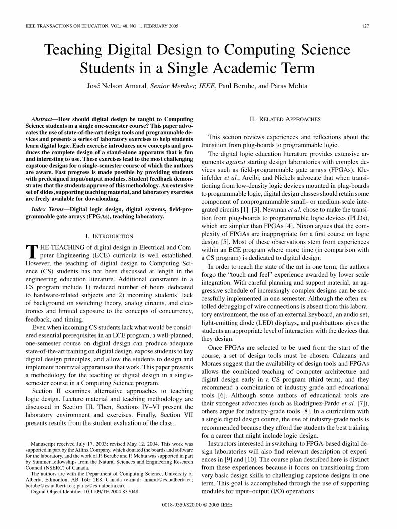
Fig. 1. Development boards as used in the laboratory, from XESS Corporation.
III. LECTURING METHODOLOGY
In-class time is effectively used by relying on an extensiveset of slides for the lectures [11]. These slides are carefully de-signed to allow in-class interaction with the students.1 Anima-tion techniques are often used to allow in-class quizzes. Stu-dents are asked to put printouts of slides aside and to take outpaper and pencil to solve these quizzes. Logic gate constructionfollows Patt’s abstraction of the light switch to represent a tran-sistor [12]. The initial chapters of the adopted textbook, by Wak-erly, discuss number systems and electronic technology [13].This material is made into reading assignments with scheduledten-minute in-class quizzes. Homework assignments are regu-larly assigned, but in order to rationalize teaching assistants’(TAs’) time, the solutions are not collected for grading. Instead,short, scheduled in-class quizzes test the same material at thehomework due date.
The use of FPGAs requires the inclusion of very high speedintegrated circuit (VHSIC) hardware description language(VHDL) learning in the one-term course. The laboratory exer-cises were designed to minimize the in-class time dedicated toVHDL. The students are told on the first day of class that theyare expected to learn VHDL on their own.2 Once this level ofexpectation is set, only two 50-minute lectures are required todiscuss the most important principles of VHDL modeling inclass.
The careful use of technology and old-fashioned commonsense allows the development of a challenging but exciting one-term digital design course for a CS curriculum. Students nowlook forward to, and praise (Section VII), this third-year op-tional class in the program.
IV. LABORATORY ENVIRONMENT
The exercises where used in a laboratory with 20 worksta-tions, with each workstation having an XSA-50 FPGA boardand an XStend daughter-board.3 Desk-fastened custom plastic
1Slides, exams, quizzes, and laboratory assignments are publicly available atwww.cs.ualberta.ca/~amaral/courses/329.
2In this case, the CS background is an advantage because third-year CS stu-dents are familiar with learning new programming languages on their own.
3XSA-50 and XStend are products of the X Engineering Software Systems(XESS) Corporation (www.xess.com).
enclosures minimize wear and tear, accidental damage, or unsu-pervised removal and allows 24-hour operation for the labora-tory. Fig. 1(a) shows the enclosed boards connected to a parallelport of a host computer, a power supply, a PS\2 keyboard, and aheadphone set. Fig. 1(b) is a closer view of the XStend and theXSA-50 outside the plexiglass encasing.
A. Hardware and Software Environments
The XStend boards have an eight-segment bar-graph LEDused to display binary values, a seven-segment digital LED usedas an alphanumerical display, and a stereo codec used for audiooutput. Inputs are accepted through the buttons on the XStendboard, through the parallel port data lines, and from a keyboardattached to the PS\2 port. Students are provided with a moduleto interface with the keyboard. Once learned, this interface isreused in several exercises. The XSA’s 8-MB dynamic randomaccess memory (DRAM) and 128-KB Flash memories are usedto create designs that function without constant input from theuser.
The Xilinx Integrated Software Environment (ISE) 5.2iis used for design entry. ISE presents a hierarchical view ofthe design process that clearly illustrates the dependenciesand sequencing of implementation tasks. VHDL Simili fromSonata Electronic Design Automation (EDA) is used fortest-bench-based simulation. VHDL Simili is more intuitiveand user friendly for beginner students than the industry-strongModelSim from Mentor Graphics. Test-bench writing is chal-lenging to the novice designer; thus, students are providedrudimentary test benches for all but the capstone laboratories.
1) Test Benches: When using a test bench, the student candetect errors and identify signals that are assigned incorrectly.Test benching also allows for easier grading of laboratory ex-ercises. TAs are provided with test benches that are not pub-lished to the students and, hence, can do a thorough, fast, andfair comparison of designs. A simplified test-bench driver is sup-plied to allow students to perform initial testing and to providethe basis for a more complete test bench. Test-bench inputs forself-checking test benches are supplied as a text file, and the cor-responding correct outputs are provided in another file. If sim-ulated outputs do not match supplied outputs, an error messageis generated.
AMARAL et al.: TEACHING DIGITAL DESIGN TO COMPUTING SCIENCE STUDENTS 129
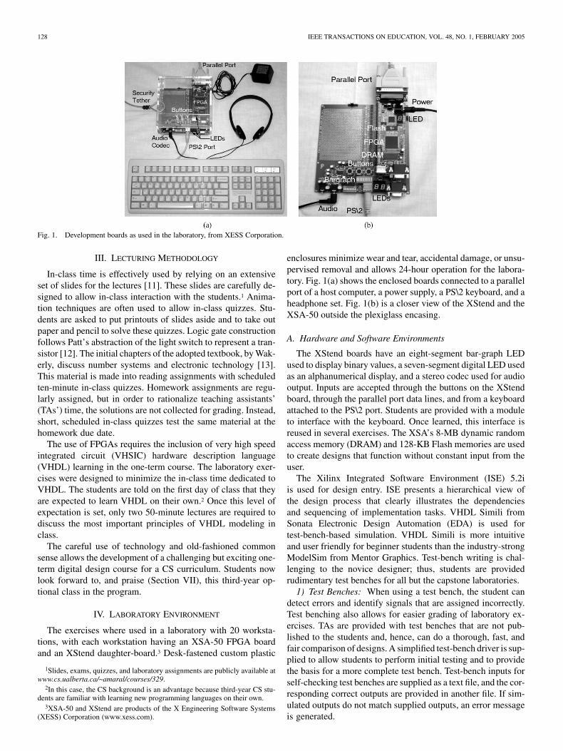
Fig. 2. Block diagram for the scrolling message display system.
2) Demonstration: Successfully simulated designs may notnecessarily work in hardware since timing issues and hazardsmay not be simulated completely. In addition, complex behav-iors, such as the PS\2 protocol, are not simulated; instead, thePS\2 output is simulated. Hence, if the keyboard interface isnot correctly connected to the keyboard pins, this error wouldnot be simulated. Conversely, unsuccessful simulations do notimply total failure. To allow partial grades for partial function-ality, demonstration is the only way to assess the extent of thestudent effort.
V. TERM LABORATORY EXERCISES
This section provides only brief descriptions of the firstfive laboratories. Complete descriptions and VHDL modulesare found in the course Web page. Initial laboratory exercisesfamiliarize the students with the integrated development envi-ronment and with the design of combinatorial circuits.
A. Simple Alarm System
Design the logic for the control circuit of an alarm from a nat-ural language specification. The students are required to buildboth a schematic diagram and a VHDL design so that they cancontrast the advantages of both input formats.
B. Parity Checker
Design a circuit to read a hexadecimal digit from a keyboardand calculate its parity. The parity is displayed as a numericaldigit on a seven-segment LED, while the input is representedin binary on a bar graph LED. This laboratory introduces theboard’s I/O features, structural VHDL, and the VHDL Similisimulator.
C. Treehouse Encryption
Implement a bit-scrambling encryption algorithm. A standardPS\2 keyboard is used as input. Complete modules in VHDLand partially completed VHDL code are provided for the stu-dents to examine. Portions of the design are provided as speci-fications that require the students to build a hierarchical designusing submodules.
D. Scrolling Message Display
Produce a scrolling message in the two neighboring seven-segment LEDs of the XStend boards. The message to be dis-played is stored in off-chip memory in ASCII format. The end
of the message is detected by a special ASCII code. When theend of the message is reached, the message has to be scrolledin reverse order until the beginning of the message is reached,whereupon it will scroll forward again. A PS\2 keyboard is usedto control the speed of the scrolling. A block diagram for thislaboratory is shown in Fig. 2.
Besides the VHDL code for the I/O interfaces, the studentsare also given a skeleton for the design of the address-LEDmultiplexer and for the control unit. Completion of the code inthese skeletons will produce the basic functionality of the simplescrolling device. However, to obtain the continuing forward–re-verse scrolling function, the control unit must be redesigned.With a functional forward-scrolling system, the use of a hierar-chical design for the new control unit should be natural. In ad-dition, the control of the scrolling speed through the keyboardinterface requires that the students implement a variable counterin the control unit to determine how often a new character hasto be read from the off-chip memory. This exercise introducescounters, multiplexing, and component reuse and practices hi-erarchical design.
E. Multimode Calculator
Design a finite-state machine (FSM) that implements a two-digit hexadecimal calculator that handles input expressions inprefix, infix, or postfix form. The PS\2 interface is used both toselect the operation mode and to input the operations to be per-formed by the calculator. The seven-segment LEDs display theresult of the calculations and the current operation mode. Nu-merical inputs are two digits. Addition, subtraction, and multi-plication operations are supported in all modes.
This calculator can be implemented as a single, large FSM inwhich numerical inputs, arithmetic operators, and commands tochange the mode of operation are the inputs. However, a betterstrategy is for the student to break this FSM into smaller ones.For this laboratory, no block diagrams are provided, and thestudents are free to build their design however they desire.
VI. CAPSTONE DESIGNS
The final laboratory exercise is the capstone for the class.A collection of different exercises can be rotated as the cap-stone design in order to keep the course interesting and intro-duce some variation in the undergraduate program. Currently,there are two capstone designs: a music recorder and an inter-active game.
130 IEEE TRANSACTIONS ON EDUCATION, VOL. 48, NO. 1, FEBRUARY 2005
A. Music Recorder
Music Recorder is the design of a musical keyboard playedthrough the audio codec whose output can be recorded to andplayed back from the RAM. The design must also be able totranspose the music up or down by as much as one octave. Theamount of transposition is set from the keyboard. Students aregiven only a natural (i.e., English) language specification of thedesign.
Students are provided with the keyboard interface and a se-ries of VHDL modules that produce an audio interface withthe codec that translates Musical Instrument Digital Interface(MIDI) note signals into sounds. Students are responsible forthe design of the control modules. As a bonus, the students mayexpand their design to display the transposition of notes on theLEDs. This requirement demands that shared lines between theLEDs and the RAM memory be multiplexed.
Important features of this laboratory are outlined hereafter.
1) Tones must be held while a keyboard key is depressedand stopped when the key is released (therefore, both keypresses and releases must be monitored).
2) RAM must be accessed for both reading and writing,meaning that control signals must be properly generated.
3) Control inputs can arrive from the keyboard asynchro-nously.
A successful design depends on the proper interaction of severalfairly complex state machines.
B. Type, Type, Revolution!
Type, Type, Revolution! is based on a popular arcade gameof similar name, “Dance, Dance, Revolution!” This assignmentinvolves designing an interactive game using FPGAs. Studentsare given only high-level design specifications for this game.
The game itself is fairly simple: the system reads an instruc-tion from memory, selected from a set of directional keys (up,down, left, and right), and displays the instruction on two seven-segment LEDs on the XStend board. The user must then pressthe key corresponding to the displayed instruction before thenext instruction is displayed. Three mistakes or missed keysare allowed before the game ends. At the end of the game,the number of sequences completed is displayed. When the se-quence ends, the user is credited one additional allowable mis-take (to a maximum total of three), and the sequence repeats.Students are also encouraged to develop additional functionalityfor bonus marks. Suggestions include increasing the game speedafter each completed sequence and making the length of time foreach key variable.
VII. STUDENT FEEDBACK
This section presents results from a standard student evalua-tion of courses and a summary of a qualitative evaluation of thelaboratories through written comments in the laboratory reports.
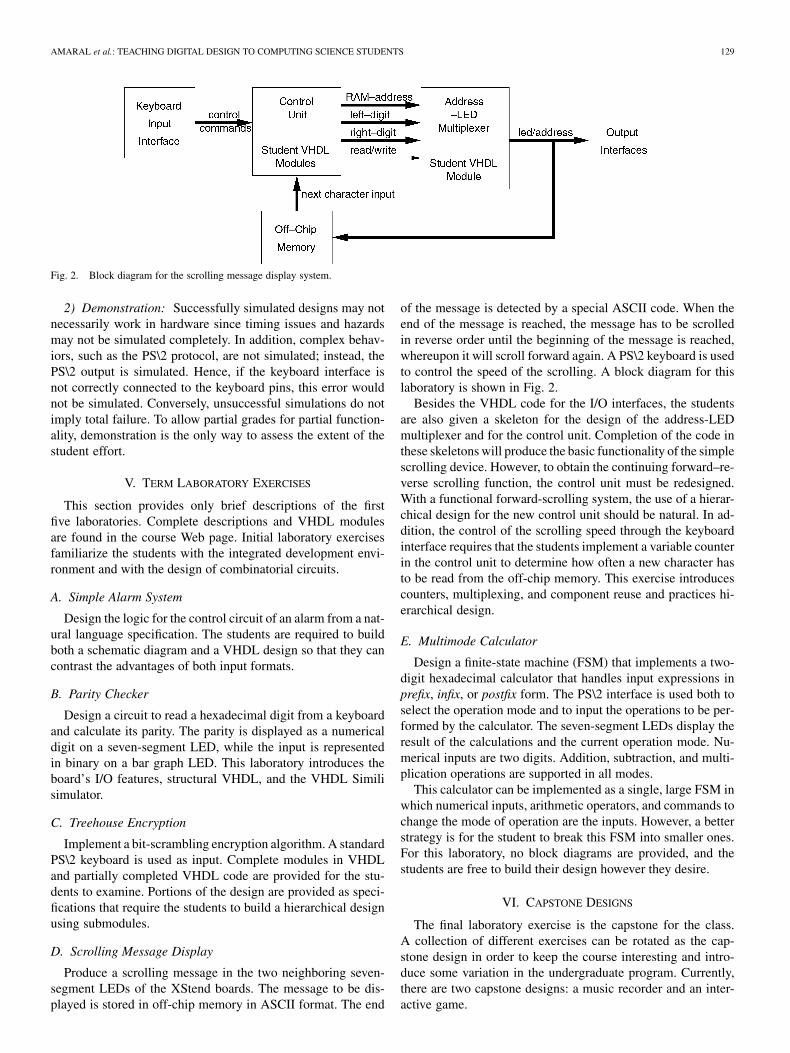
At the University of Alberta, Edmonton, AB, Canada, stan-dard student evaluations of courses are conducted in every term.Table I shows the number of students registered and the numberof responses to the in-class student evaluation for this course.
Table II reports the answers to four questions that should berelevant for instructors interested in adopting a similar teaching
TABLE INUMBER OF RESPONDENTS TO THE STUDENT
EVALUATION OF THE COURSE
TABLE IISTUDENTS’ REACTION TO VARIOUS STATEMENTS EVALUATING THE COURSE
methodology for digital design. The class was taught by thesame instructor in all four years. The numbers under the “Per-centile” column indicate how the answers compare with othercourses taught during the same term at the University of Al-berta. For instance 75 of 162 means that when comparedwith a cohort of 162 courses that offer laboratory, the answersfor 2000 were more positive than 75% of the courses.4 For theother three questions, the answers are compared with all ses-sions evaluated in that term at the University of Alberta. Thedisruption caused by the adoption of VHDL and FPGAs causeda significant reduction in the number of students who considerthe laboratory environment appropriate in 2001 and 2002. How-ever, on the third edition of the new course (2003), the studentresponses were more positive than before these changes.
As glitches were eliminated from the laboratory experiments,the software environment and lecture material were improved.The instructor acquired experience teaching the class; thus, theevaluation of the course improved significantly. The most sig-nificant changes are in the number of students who considerthe workload appropriate and the course content excellent. Theworkload of this course is higher than in similar courses in otheruniversities, and it is also higher than similar courses in the sameterm at the University of Alberta. However, over the three-yearperiod in which the changes were implemented, the expectationof the students changed, and the additional effort required forthe course is now considered “normal” by the students. A clearevidence of the students’ approval of the changes and of their
4The size of the cohort for some questions and years was not published bythe university, but it should be similar with previous years.
AMARAL et al.: TEACHING DIGITAL DESIGN TO COMPUTING SCIENCE STUDENTS 131
benefit from the course is that this elective class and the enroll-ment has not dropped in spite of the additional effort that theclass requires.
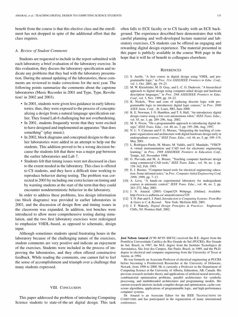
A. Review of Student Comments
Students are requested to include in the report submitted witheach laboratory a brief evaluation of the laboratory exercise. Inthis evaluation, they discuss the laboratory specification and in-dicate any problems that they had with the laboratory presenta-tion. During the annual updating of the laboratories, these com-ments are reviewed to make corrections for the next year. Thefollowing points summarize the comments about the capstonelaboratories (Music Recorder in 2001 and Type, Type, Revolu-tion! in 2002 and 2003).
• In 2001, students were given less guidance in early labora-tories; thus, they were exposed to the process of conceptu-alizing a design from a natural language specification ear-lier. They found Lab 6 challenging but not overburdening.
• In 2001, students frequently wrote that they were excitedto have designed and implemented an apparatus “that doessomething” (play music).
• In 2002, block diagrams and conceptual designs to the ear-lier laboratories were added in an attempt to help out thestudents. This addition proved to be a wrong decision be-cause the students felt that there was a major gap betweenthe earlier laboratories and Lab 7.
• Students felt that timing issues were not discussed in classto the extent needed in the laboratory. This class is offeredto CS students, and they have a difficult time working toreproduce behavior during testing. The problem was cor-rected in 2003 by including one extra lecture on timing andby warning students at the start of the term that they couldencounter nondeterministic behavior in the laboratory.
In order to address these problems, less design information(no block diagrams) was provided in earlier laboratories in2003, and the discussion of design flow and timing issues inthe classroom was expanded. In addition, test benches wereintroduced to allow more comprehensive testing during simu-lation, and the two first laboratory exercises were redesignedto emphasize VHDL-based, as opposed to schematic, designinput.
Although sometimes students spend frustrating hours in thelaboratory because of the challenging nature of the exercises,student comments are very positive and indicate an enjoymentof the exercises. Students were included in the process of im-proving the laboratories, and they often offered constructivefeedback. While reading the comments, one cannot fail to feelthe sense of accomplishment and triumph over a challenge thatmany students expressed.
VIII. CONCLUSION
This paper addressed the problem of introducing ComputingScience students to state-of-the-art digital design. This task
often falls to ECE faculty or to CS faculty with an ECE back-ground. The experience described here demonstrates that withcareful planning and well-developed lecture material and lab-oratory exercises, CS students can be offered an engaging andrewarding digital design experience. The material presented inthis paper is publicly available in the course Web page in thehope that it will be of benefit to colleagues elsewhere.
REFERENCES
[1] S. Areibi, “A first course in digital design using VHDL and pro-grammable logic,” in Proc. 31st ASEE/IEEE Frontiers in Educ. Conf.,vol. 1, Oct. 2001, pp. 19–23.
[2] M. W. Kleinfelder, M. D. Gray, and L.-C. G. Dudevoir, “A hierarchicalapproach to digital design using computer-aided design and hardwaredescription languages,” in Proc. 29th ASEE/IEEE Frontiers in Educ.Conf., vol. 3, Nov. 1999, pp. 18–22.
[3] K. Nickels, “Pros and cons of replacing discrete logic with pro-grammable logic in introductory digital logic courses,” in Proc. 2000ASEE Annu. Conf. , St. Louis, MO, June 2000.
[4] K. E. Newman, J. O. Hamblen, and T. S. Hall, “An introductory digitaldesign course using a low-cost autonomous robot,” IEEE Trans. Educ.,vol. 45, no. 3, pp. 289–296, Aug. 2002.
[5] M. S. Nixon, “On a programmable approach to introducing digital de-sign,” IEEE Trans. Educ., vol. 40, no. 3, pp. 195–206, Aug. 1997.
[6] N. L. V. Calazans and F. G. Moraes, “Integrating the teaching of com-puter organization and architecture with digital hardware design early inundergraduate courses,” IEEE Trans. Educ., vol. 44, no. 5, pp. 109–119,May 2001.
[7] L. Rodríguez-Pardo, M. Moure, M. Valdés, and E. Mandado, “VISCP:A virtual instrumentation and CAD tool for electronic engineeringlearning,” in Proc. 1998 ASEE/IEEE Frontiers in Education Conf.,Tempe, AZ, November 1998.
[8] G. Puvvada and M. A. Breuer, “Teaching computer hardware designusing commercial CAD tools,” IEEE Trans. Educ., vol. 36, no. 1, pp.158–162, Feb. 1993.
[9] E. I. Boemo, “Computer-based tools for electrical engineering educa-tion: Some informal notes,” in Proc. Computer Aided Engineering Conf.1999, 1999, pp. 7–13.
[10] A. Leva, “A hands-on experimental laboratory for undergraduatecourses in automatic control,” IEEE Trans. Educ., vol. 46, no. 2, pp.263–272, May 2003.
[11] J. N. Amaral. (2003) Cmput329 Webpage. [Online]. Available:http://www.cs.ualberta.ca/ amaral/courses/329
[12] Y. N. Patt and S. J. Patel, Introduction to Computing Systems: From Bits& Gates to C & Beyond. New York: McGraw-Hill, 2001.
[13] J. F. Wakerly, Digital Design Principles & Practices. EnglewoodCliffs, NJ: Prentice-Hall, 2002.
José Nelson Amaral (S’90–M’95–SM’01) received the B.E. degree from thePontifícia Universidade Católica do Rio Grande do Sul (PUCRS), Rio Grandedo Sul, Brazil, in 1987, the M.E. degree from the Instituto Tecnológico deAeronáutica, São José dos Campos, São Paulo, Brazil, in 1989, and the Ph.D.degree in electrical and computer engineering from the University of Texas atAustin, in 1994.
He was formerly an Associate Professor of electrical engineering at PUCRSbefore becoming a Postdoctoral Researcher at the University of Delaware,Newark, from 1998 to 2000. He is currently a Professor in the Department ofComputing Science at the University of Alberta, Edmonton, AB, Canada. Hisprevious research includes theory and applications of artificial neural networks,combinatorial optimization problems, parallel architectures for symbolicprocessing, and multithreaded architectures and programming models. Hiscurrent research interests include compiler design and optimization, cache-con-scious algorithms, applications of programmable logic, and high-performancecomputer systems.
Dr. Amaral is an Associate Editor for the IEEE TRANSACTIONS ON
COMPUTERS and has participated in the organization of many internationalconferences.

132 IEEE TRANSACTIONS ON EDUCATION, VOL. 48, NO. 1, FEBRUARY 2005
Paul Berube received the B.Sc. degree in computing science from the Univer-sity of Alberta, Edmonton, AB, Canada, in 2003. He is currently working towardthe M.Sc. degree in computing science at the same university.
His research interests include compiler design and optimization, computerarchitecture, and programmable logic devices.
Mr. Berube was awarded a competitive Natural Sciences and EngineeringResearch Council (NSERC) of Canada graduate fellowship in 2003.
Paras Mehta received the B.Sc. degree in computing science from the Univer-sity of Alberta, Edmonton, AB, Canada, in 2004.
His current research interest is on parallel programming systems.Mr. Mehta received an Undergraduate Student Research Award (USRA) from
the Natural Sciences and Engineering Research Council (NSERC) of Canada in2003 and 2004. He is also a recipient of the Terence Holowach Memorial Prizeand of the Amdahl Academic Achievement Scholarship in Computing Science.