te430vx motherboard technical product specification · te430vx motherboard technical product...
TRANSCRIPT
TE430VXMotherboardTechnical Product Specification
Order Number 281817-003
May 1996
Revision History
Revision Revision History Date
-003 Fixed drawing designators, added USB module, corrected inaccuracies,reworded sections for clarity, removed reference to Creative Labs Vibra16S with Yamaha FM Synthesis
5/96
-002 Changed Name of product from Advanced/TE to TE430VX throughout 4/96
-001 Preliminary release of the TE430VX Technical Product Specification. 3/96
This product specification applies only to standard TE430VX ATX motherboards with BIOSidentifier 1.00.01.CY0.
Changes to this specification will be published in the TE430VX Motherboard Specification Updatebefore being incorporated into a revision of this document.
Intel Corporation disclaims all warranties and liabilities for the use of this document and the information contained herein,Information in this document is provided in connection with Intel products. No license, express or implied, by estoppel orotherwise, to any intellectual property rights is granted by this document. Except as provided in Intel’s Terms and Conditions ofSale for such products, Intel assumes no liability whatsoever, and Intel disclaims any express or implied warranty, relating tosale and/or use of Intel products including liability or warranties relating to fitness for a particular purpose, merchantability, orinfringement of any patent, copyright or other intellectual property right. Intel products are not intended for use in medical, lifesaving, or life sustaining applications.
Intel retains the right to make changes to specifications and product descriptions at any time, without notice.
The TE430VX motherboard may contain design defects or errors known as errata. Current characterized errata are available onrequest.
Contact your local Intel sales office or your distributor to obtain the latest specifications before placing your product order.
† Third-party brands and names are the property of their respective owners.
Copies of documents which have an ordering number and are referenced in this document, or other Intel literature, may beobtained from:
Intel CorporationP.O. Box 7641Mt. Prospect, IL 60056-7641
or call in North America 1-800-879-4683, Europe 44-0-1793-431-155, France 44-0-1793-421-777,
Germany 44-0-1793-421-333, Japan (fax only) 81-0-120-478-832, other Countries 708-296-9333
Copyright 1996, Intel Corporation
iii
Table of Contents
1 Motherboard Description1.1 Overview ............................................................................................................7
1.2 Motherboard Manufacturing Options..................................................................9
1.3 Form Factor .......................................................................................................9
1.4 Microprocessor.................................................................................................10
1.4.1 Microprocessor Upgrade ....................................................................10
1.5 Memory ............................................................................................................10
1.5.1 System Memory..................................................................................10
1.5.2 Second Level Cache...........................................................................11
1.6 Chipset .............................................................................................................11
1.6.1 82430VX System Controller (TVX) .....................................................11
1.6.2 82430VX Data Path (TDX)..................................................................12
1.6.3 PCI ISA/IDE Xcelerator (PIIX3)...........................................................12
1.6.4 IDE SUPPORT....................................................................................12
1.7 Ultra I/O Interface Controller (SMC FDC37C93FR) .........................................13
1.7.1 Floppy controller .................................................................................13
1.7.2 Keyboard and mouse interface...........................................................13
1.7.3 Real time clock, CMOS RAM and battery...........................................13
1.7.4 IrDA (infra-red) support.......................................................................14
1.7.5 Consumer IR Support .........................................................................14
1.7.6 Parallel port.........................................................................................14
1.8 Graphics Subsystem (S3 Trio64V+).................................................................14
1.8.1 Resolutions supported ........................................................................15
1.8.2 Graphics Drivers and Utilities..............................................................15
1.9 Audio Subsystem (Creative Labs Vibra 16C)...................................................15
1.9.1 Vibra 16C resource map.....................................................................16
1.9.2 Audio Drivers ......................................................................................16
1.10 Motherboard Connectors .................................................................................17
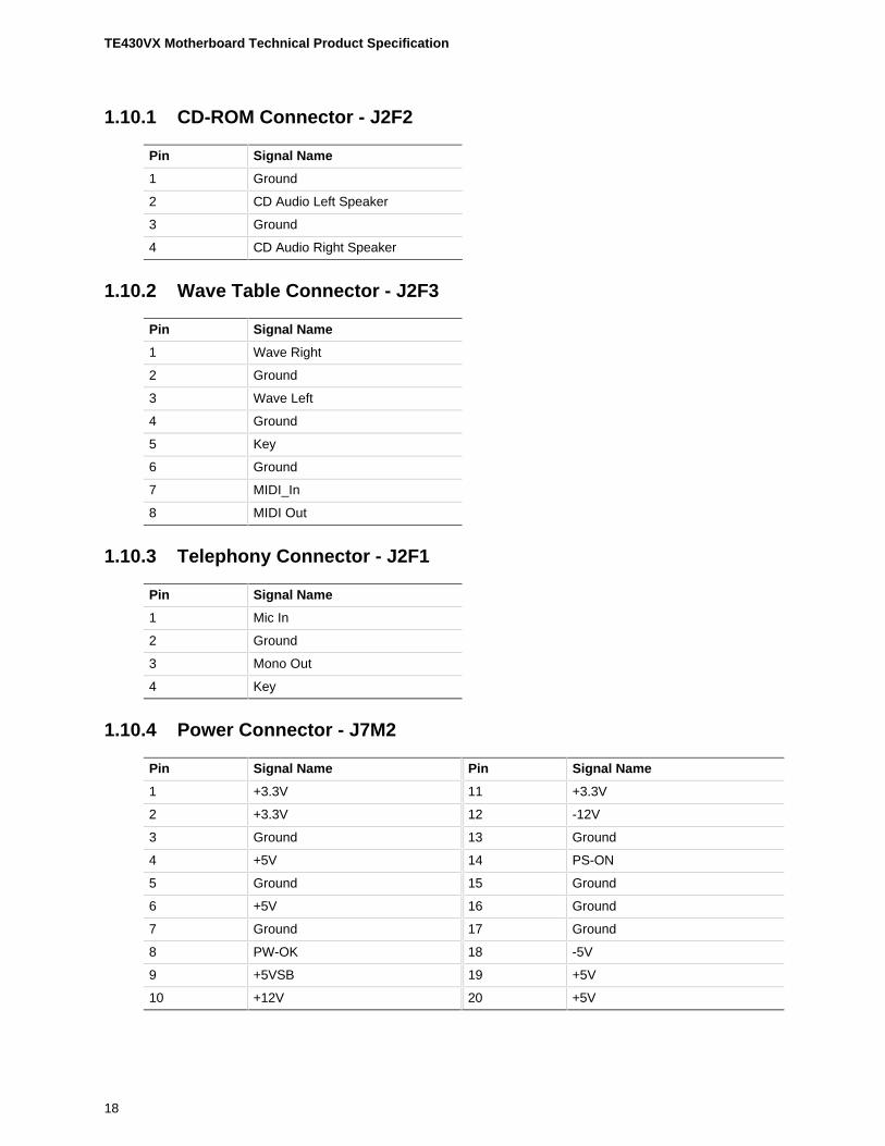
1.10.1 CD-ROM Connector - J2F2 ................................................................18
1.10.2 Wave Table Connector - J2F3............................................................18
1.10.3 Telephony Connector - J2F1 ..............................................................18
TE430VX Motherboard Technical Product Specification
iv
1.10.4 Power Connector - J7M2 ....................................................................18
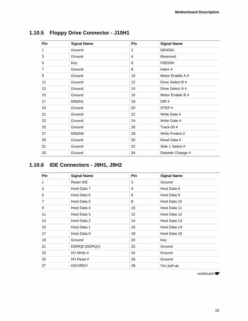
1.10.5 Floppy Drive Connector - J10H1 ........................................................19
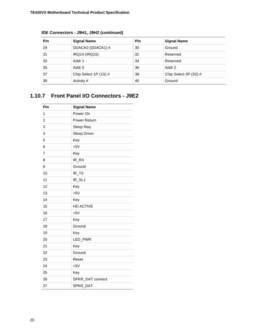
1.10.6 IDE Connectors - J9H1, J9H2.............................................................19
1.10.7 Front Panel I/O Connectors - J9E2.....................................................20
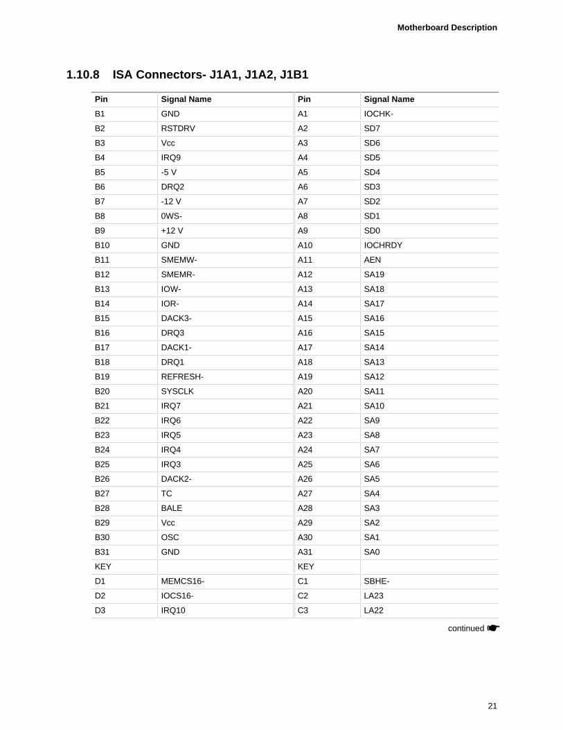
1.10.8 ISA Connectors- J1A1, J1A2, J1B1 ....................................................21
1.10.9 PCI Connectors - J2C1, J2D1, J2E1, J2E2 ........................................22
1.10.10 Power Supply Connectors ..................................................................23
1.10.11 Front panel Connectors ......................................................................24
1.10.12 Back Panel Connectors ......................................................................26
1.10.13 Add-in Board Expansion Connectors..................................................27
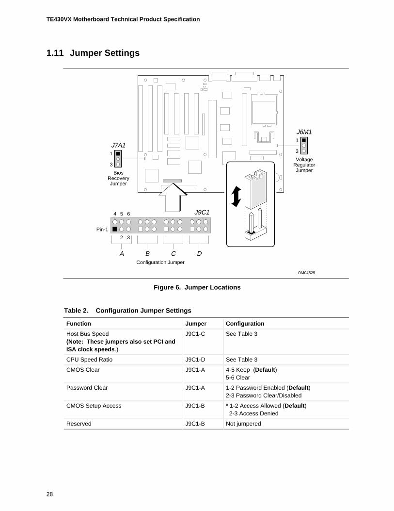
1.11 Jumper Settings ...............................................................................................28
1.11.1 CPU Configuration (J9C1-C, D)..........................................................29
1.11.2 Clear CMOS (J9C1-A, Pins 4,5,6) ......................................................29
1.11.3 Password clear (J9C1-A, Pins 1,2,3) ..................................................29
1.11.4 CMOS Setup Access (J9C1-B, Pins 1,2,3).........................................29
1.11.5 CPU Voltage (J6M1)...........................................................................30
1.11.6 BIOS Recovery (J7A1)........................................................................30
1.12 Reliability..........................................................................................................30
1.13 Environmental ..................................................................................................30
1.14 Power Consumption.........................................................................................31
1.15 Regulatory Compliance....................................................................................31
1.15.1 Safety..................................................................................................31
1.15.2 EMI .....................................................................................................32
1.15.3 Product Certification Markings............................................................32
1.15.4 Installation Requirements ...................................................................33
2 Motherboard Resources2.1 Memory Map ....................................................................................................37
2.2 I/O Map ............................................................................................................37
2.3 oft-Off Control...................................................................................................39
2.4 CI Configuration Space Map ............................................................................39
2.5 MA Channels....................................................................................................39
2.6 nterrupts...........................................................................................................40
Contents
v
3 Motherboard BIOS and Setup Utility3.1 Introduction ......................................................................................................41
3.2 BIOS Flash Memory Organization ...................................................................41
3.3 BIOS Upgrades ................................................................................................42
3.4 PCI IDE Support...............................................................................................42
3.5 PCI Auto-configuration .....................................................................................43
3.6 ISA Plug and Play ............................................................................................43
3.7 Advanced Power Management ........................................................................44
3.8 Language Support............................................................................................44
3.9 Boot Options ....................................................................................................44
3.10 Flash LOGO Area ............................................................................................45
3.11 Setup Enable Jumper.......................................................................................45
3.12 BIOS Setup Program .......................................................................................45
3.12.1 Overview of the Setup Menu Screens ................................................45
3.12.2 Main BIOS Setup Screen....................................................................46
3.12.3 Floppy Options Subscreen .................................................................47
3.12.4 IDE Device Configuration Subscreen .................................................48
3.12.5 Boot Options Subscreen.....................................................................49
3.12.6 Advanced Screen ...............................................................................50
3.12.7 Peripheral Configuration Subscreen...................................................51
3.12.8 Advanced Chipset Configuration Subscreen ......................................52
3.12.9 Power Management Configuration Subscreen ...................................53
3.12.10 Plug and Play Configuration Subscreen .............................................54
3.12.11 Security Screen ..................................................................................55
3.12.12 Security Screen Options .....................................................................56
3.12.13 Exit Screen .........................................................................................56
4 Error Messages and Beep Codes4.1 BIOS Beep Codes............................................................................................59
4.2 PCI Configuration Error Messages ..................................................................59
4.3 BIOS Error Messages ......................................................................................60
4.4 ISA NMI Messages ..........................................................................................61

7
1 Motherboard Description
1.1 Overview
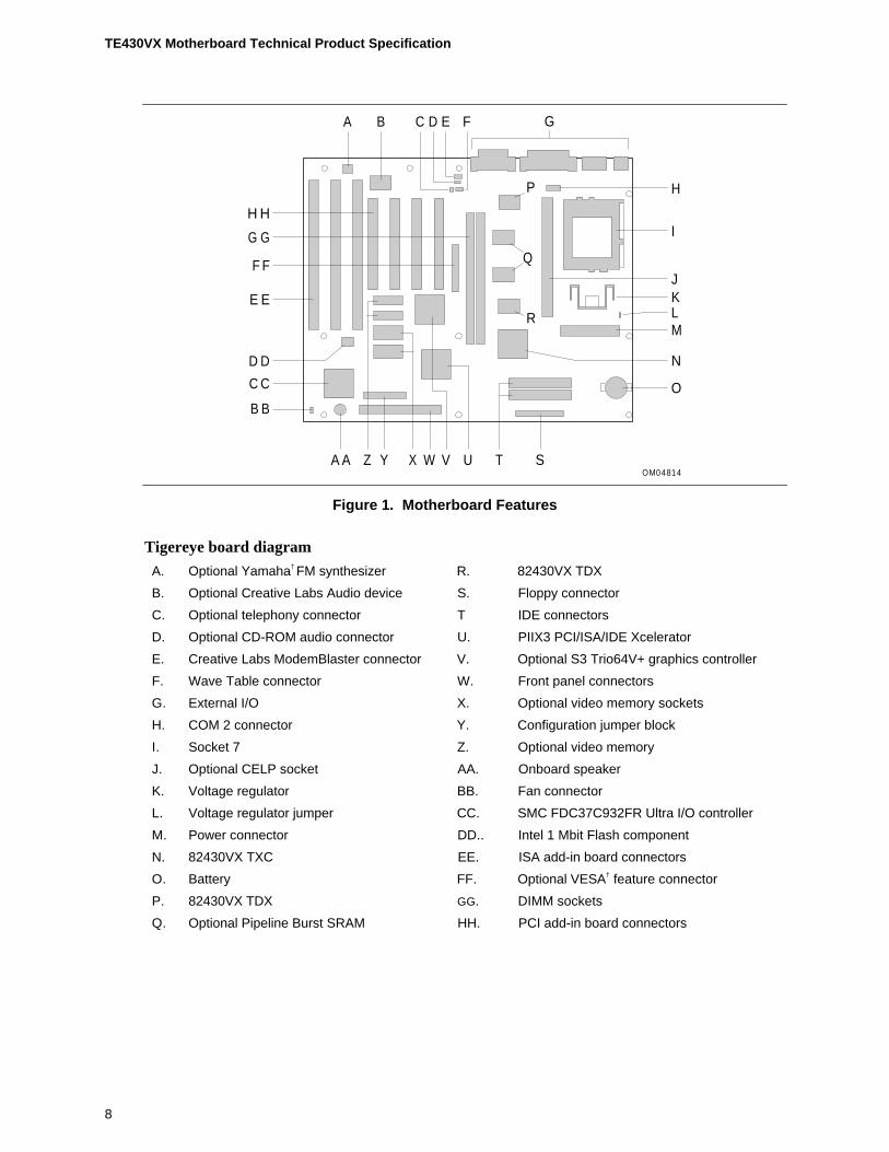
The TE430VX design accepts Pentium processors operating at 75 MHz, 90 MHz, 100 MHz,120 MHz, 133 MHz, 150 MHz, 166 MHz, and 200MHz. There is an option of having 256 KB ofPipeline Burst SRAM soldered onto the motherboard, or a Card Edge Low Profile (CELP)connector for cache expandability. The memory subsystem is designed to support up to 128 MB ofEDO DRAM, or up to 64 MB of a new memory architecture called SDRAM, in standard 168-pinDIMM sockets. A type 7 Pentium OverDrive socket provides upgrades to future OverDriveprocessors.
The TE430VX motherboard utilizes Intel's 82430VX PCISet. The 82430VX PCIset contains anintegrated PCI Bus Mastering IDE controller with two high performance IDE interfaces for up tofour IDE devices (such as hard drives, CD-ROM readers, and so forth). The SMC FDC37C932FRUltra I/O controller integrates the standard PC I/O functions: floppy interface, two FIFO serialports, one EPP/ECP capable parallel port, a Real Time Clock, keyboard controller, and support foran IrDA† compatible infrared interface. To provide for the increasing number of multimediaapplications, a Creative Labs Vibra16C audio codec is integrated onto the motherboard. The Vibra16C provides 16-bit stereo, Sound Blaster† Pro compatible audio. Integrated onto the motherboardalso is the S3† Trio64† V+ video subsystem. Up to four PCI local bus slots provide a highbandwidth data path for data-movement intensive functions such as video or networking, and up tothree ISA slots complete the I/O mix. A total of six expansion slots may be populated with fulllength add-in cards: one PCI and ISA slot share the same chassis I/O panel.
TE430VX Motherboard Technical Product Specification
8
OM04814
B C GD E
I
JK
H
M
O
Q
P
R
WY STUA A XZ V
F F
H H
E E
A
G G
C C
F
ND D
L
B B
Figure 1. Motherboard Features
Tigereye board diagram
A. Optional Yamaha† FM synthesizer R. 82430VX TDX
B. Optional Creative Labs Audio device S. Floppy connector
C. Optional telephony connector T IDE connectors
D. Optional CD-ROM audio connector U. PIIX3 PCI/ISA/IDE Xcelerator
E. Creative Labs ModemBlaster connector V. Optional S3 Trio64V+ graphics controller
F. Wave Table connector W. Front panel connectors
G. External I/O X. Optional video memory sockets
H. COM 2 connector Y. Configuration jumper block
I. Socket 7 Z. Optional video memory
J. Optional CELP socket AA. Onboard speaker
K. Voltage regulator BB. Fan connector
L. Voltage regulator jumper CC. SMC FDC37C932FR Ultra I/O controller
M. Power connector DD.. Intel 1 Mbit Flash component
N. 82430VX TXC EE. ISA add-in board connectors
O. Battery FF. Optional VESA† feature connector
P. 82430VX TDX GG. DIMM sockets
Q. Optional Pipeline Burst SRAM HH. PCI add-in board connectors
Motherboard Description
9
1.2 Motherboard Manufacturing Options• Creative Labs Vibra 16C Audio• S3 Trio64V+ Video• CELP Module or soldered 256k PBSRAM with GWE• USB• Split Plane Voltage Support for Socket 7• Flash Recovery
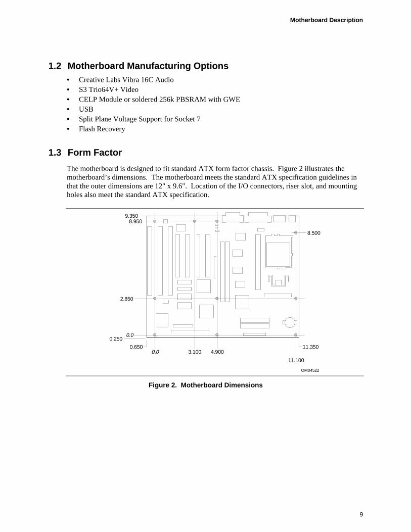
1.3 Form Factor
The motherboard is designed to fit standard ATX form factor chassis. Figure 2 illustrates themotherboard’s dimensions. The motherboard meets the standard ATX specification guidelines inthat the outer dimensions are 12" x 9.6". Location of the I/O connectors, riser slot, and mountingholes also meet the standard ATX specification.
OM04522
8.950
2.850
0.0
9.350
8.500
0.00.250
0.650 11.3503.100 4.900
11.100
Figure 2. Motherboard Dimensions
TE430VX Motherboard Technical Product Specification
10
1.4 Microprocessor
The motherboard is designed to operate with 3.3 volt Pentium Processors running at 75, 90, 100,120, 133, 150, 166, and 200MHz. An onboard linear voltage regulator circuit provides therequired 3.3 volts from the 5.0 volt tap of the power supply. An on-board jumper enables use ofVRE specified processors.
The Pentium processor maintains full backward compatibility with 8086, 80286, i386 andIntel486 processors. It supports both read and write burst mode bus cycles and also includesseparate 8 KB on-chip code and data caches that employ a write-back policy.
The Pentium processor is an advanced numeric coprocessor that significantly increases the speed offloating point operations, while maintaining backward compatibility with i486DX mathcoprocessor and complying to ANSI/IEEE standard 754-1985.
This motherboard does not support the keep-out zones around the socket 7 that allow use of a“piano wire” type heatsink clip. Intel recommends using only metal heatsink clips.
1.4.1 Microprocessor UpgradeThe motherboard provides a 321-pin Socket 7 ZIF processor socket. Socket 7 supports upgrades tohigher performance Pentium OverDrive processors.
1.5 Memory
1.5.1 System MemoryThe motherboard provides two 168-pin DIMM(Dual Inline Memory Module) sites for DRAMmemory expansion. The sockets support 1 Meg x 64 (8 MB), 2 Meg x 64 (16 MB), and 4 Meg x64 (32 MB) SDRAM DIMM modules and 1 Meg x 64 (8 MB), 2 Meg x 64 (16 MB), 4 Meg x 64(32 MB) and 8 Meg x 64 (64 MB) EDO(Extended Data Out) DIMM modules. For systemsconfigured with EDO or SDRAM DIMM modules, minimum memory size is 8MB for EDOsystems. Maximum memory size is 128MB for EDO systems. Maximum memory size is 64MBfor SDRAM systems.
The two DIMM sockets are arranged as Bank 0 and Bank 1. Each bank consists of one socket anda 64-bit wide data path. Bank 0 only, Bank 1 only, or both banks may be populated. EDO andSDRAM may be installed in the same system. The system BIOS automatically detects memorysize and type so no jumper settings are required. Gold leaded DIMMs are required to be usedwhen adding system memory.
1.5.1.1 EDO DRAME D O (or Hyper Page) DRAM improves the DRAM read performance. EDO DRAM holds thememory data valid until the next CAS# falling edge unlike standard fast page mode DRAM, whichtri-states the memory data when CAS# negates to precharge for the next cycle. With EDO, theCAS# precharge overlaps the data valid time allowing CAS# to negate earlier while still satisfyingthe memory data valid window time.
Motherboard Description
11
1.5.1.2 SDRAMSynchronous Dynamic Random Access Memory, (SDRAM) is designed to improve main memoryperformance. SDRAM is synchronous to the memory clock unlike standard Fast Page DRAM, orEDO DRAM. All the timing is dependent on the number of memory clock cycles. This makes thetiming design simpler and makes a faster memory speed easier to achieve. Discrete SDRAMcomponents must meet the 66 MHz PC SDRAM Specification version 1.0 to function correctly.
1.5.2 Second Level CacheThe Pentium processor's internal cache can be complemented by a second level cache using high-performance Pipelined Burst SRAM with GWE (Global Write Enabled) or Asynchronous Cache.
One factory option is an integrated 256 KB direct mapped write-back second level cacheimplemented with two 32k x 32 Pipeline Burst SRAM devices that take advantage of the GlobalWrite Enable pin. A 5v 8 KB x 8 external Tag SRAM provides caching support for up to 64 MBof system memory.
A second factory option is a Type 1 CELP connector, specified by Intel’s COAST ModuleSpecification version 3.0. The Type 1 CELP connector has a keying “hip” located at one end ofthe connector. This connector allows the use of both a GWE PBSRAM COAST module, and aGWE Asynchronous COAST module. The GWE Asynchronous modules must be built for Intel’s82430VX designs and are not interchangeable with Asynchronous modules built for 82430FXdesigns. The reason for this incompatibility is the additional logic added to the 82430VX modulesto account for the GWE functionality built into the chipset.
1.6 Chipset
The Intel 82430VX PCIset consists of the 82430VX System Controller (TVX), two Data Paths(TDX) and one 82371SB PCI ISA/IDE Xcelerator (PIIX3) bridge chip.
1.6.1 82430VX System Controller (TVX)The 82430VX TVX provides all control signals necessary to drive a second level cache and theDRAM array, including multiplexed address signals. The TVX also controls system access tomemory and generates snoop controls to maintain cache coherency. The TVX comes in a 208-pinQFP package that features:
• CPU interface control• Integrated L2 write-back cache
controller Pipeline Burst SRAM 256 or 512 KB direct-mapped
• Integrated DRAM controller 64 bit path to memory Support for SDRAM and EDO
DRAM 8 MB to 128 MB main memory
• Fully synchronous PCI bus interface 25/30/33 MHz PCI to DRAM > 100 Mbytes/sec Up to 4 PCI masters in addition to
the PIIX3 and IDE
12
1.6.2 82430VX Data Path (TDX)Two 82430VX TDX data path components provide a 64-bit microprocessor to memory path. TheTDX components are controlled by the TVX. They each add one load to the PCI bus and performall of the required byte and word swapping. The TDX devices come in a 208 pin QFP package.
1.6.3 PCI ISA/IDE Xcelerator (PIIX3)The PIIX3 provides the interface between the PCI and ISA buses and integrates a dual channel fastIDE interface capable of supporting up to 4 devices. The PIIX3 integrates seven 32-bit DMAchannels, five 16-bit timer/counters, two eight-channel interrupt controllers, PCI-to-AT interruptmapping circuitry, NMI logic, ISA refresh address generation, and PCI/ISA bus arbitrationcircuitry together onto the same device. The PIIX3 comes in a 208-pin QFP package that features:
• PCI Bus and ISA Bus interface• Universal Serial Bus controller
Host/hub controller• Integrated fast IDE interface
Support for up to 4 devices PIO Mode 4 transfers up to
16 MB/sec Integrated 8 x 32-bit buffer for
bus master PCI IDE bursttransfers
Bus master mode
• PCI 2.1 compliance• Enhanced fast DMA controller• Interrupt controller and steering• Counters/timers• SMI interrupt logic and timer with
fast on/off mode
1.6.4 IDE SUPPORTThe motherboard provides two independent bus-mastering PCI IDE interfaces that support PIOMode 3 and Mode 4 devices. The system BIOS supports Logical Block Addressing (LBA) andExtended Cylinder Sector Head (ECHS) translation modes as well as ATAPI (e.g. CD-ROM)devices on both IDE interfaces. The system BIOS automatically detects IDE device transfer rateand translation mode.
Normally, programmed I/O operations require a substantial amount of CPU bandwidth. In truemulti-tasking operating systems like Windows† 95, the CPU bandwidth freed up by using busmastering IDE can be used to complete other tasks while disk transfers are occurring. When usedin conjunction with the appropriate driver for the Windows 95 environment, the IDE interface canoperate as a PCI bus master capable of supporting PIO Mode 4 devices with transfer rates of up to16 MB/sec.
Motherboard Description
13
1.7 Ultra I/O Interface Controller (SMC FDC37C93FR)
1.7.1 Floppy controllerThe SMC FDC37C93FR is software compatible with the DP8473 and 82077 floppy diskcontrollers. The floppy interface can be configured for 360 KB or 1.2 MB 5¼" media or for720 KB, 1.2 MB, 1.44 MB, or 2.88 MB 3½" media in the BIOS setup. By default, the Floppy Ainterface is configured for 1.44 MB and Floppy B is disabled. Another setup option prevents theuser from being able to write to floppy. Configuring the floppy interface for 1.25 MB 3 ½"(3-mode floppy) requires the use of special floppy drives and a driver to for the specific operatingsystem.
1.7.2 Keyboard and mouse interfacePS/2† keyboard/mouse connectors are located on the back panel side of the motherboard. The 5Vlines to these connectors are protected with a PolySwitch† circuit which acts much like a self-healing fuse, re-establishing the connection after an over-current condition is removed. While thisdevice eliminates the possibility of having to replace a fuse, care should be taken to turn off thesystem power before installing or removing a keyboard or mouse. The system BIOS can detectandcorrect keyboards and mice plugged into the wrong PS/2 style connector.
The integrated 8042 microcontroller contains the AMI Megakey keyboard/mouse controller codewhich, besides providing traditional keyboard and mouse control functions, supports Power-On/Reset (POR) password protection. The POR password can be defined by the user via the Setupprogram. The keyboard controller also provides for the following "hot key" sequences:
• <CTRL><ALT><DEL>: System software reset. This sequence performs a software reset ofthe system by jumping to the beginning of the BIOS code and running the POST operation.
• <CTRL><ALT><+> and <CTRL><ALT><->: Turbo mode selection. <CTRL><ALT><->sets the system for de-turbo mode, emulating an 25 MHz AT, and <CTRL><ALT><+> setsthe system for turbo mode. Changing the Turbo mode may be prohibited by an operatingsystem, or when the CPU is in Protected mode or virtual x86 mode under DOS.
• <CTRL><ALT><defined in setup>: A power down hot-key sequence takes advantage of theSMM features of the Pentium Processor to greatly reduce the system’s power consumptionwhile maintaining the responsiveness necessary to service external interrupts. A security hot-key sequence provides password protection to the system.
1.7.3 Real time clock, CMOS RAM and batteryThe integrated Real Time Clock (RTC) is DS1287 and MC146818 compatible and provides a timeof day clock, 100-year calendar with alarm features. The RTC can be set via the BIOS SETUPprogram. The RTC also supports 242-byte battery-backed CMOS RAM in two banks which isreserved for BIOS use. The CMOS RAM can be set to specific values or cleared to the systemdefault values using the BIOS SETUP program. Also, the CMOS RAM values can be cleared tothe system defaults by using a configuration jumper on the motherboard.
An external coin-cell style battery provides power to the RTC and CMOS memory. The batteryhas an estimated lifetime of three years if the system is not plugged into the wall socket. When thesystem is plugged in, power is supplied from the ATX power supply’s 5v standby current to extendthe life of the battery.
TE430VX Motherboard Technical Product Specification
14
1.7.4 IrDA (infra-red) supportA 5-pin interface on the front panel I/O connector is provided to allow connection to a HewlettPackard† HSDSL-1000 compatible Infra-red (IrDA) transmitter/receiver. Once the module isconnected to the front panel I/O header, Serial port 2 can be re-directed to the IrDA module. Whenconfigured for IrDA, the user can transfer files to or from portable devices such as laptops, PDA’sand printers using application software such as LapLink†. The IrDA specification provides for datatransfers at 115kbps from a distance of 1 meter.
1.7.5 Consumer IR SupportThe motherboard also has a signal pin to support Consumer IR devices(remote controls). Asoftware and hardware interface is required to implement consumer IR on with the motherboard.
1.7.6 Parallel portA 25-pin D-Sub header is provided on the back panel for a multi-mode bi-directional parallel port.The parallel port operates in standard mode, Enhanced Parallel Port (EPP) version 1.7 mode, withBIOS and Driver support, and a high speed Extended Capabilities Port (ECP) compatible mode.EPP Mode requires a driver provided by the peripheral manufacturer to operate correctly.
1.8 Graphics Subsystem (S3 Trio64V+)
The motherboard is available with an S3 Trio64 V+ SVGA graphics controller with 1 MB ofgraphics memory upgradeable to 2 MB. The graphics DRAM can be upgraded to 2 MB byinstalling two 256 KB x 16 SOJ memory devices in the provided sockets. The Trio64 V+ has a64-bit graphics engine and incorporates the S3 Streams Processor that enables the device to convertYUV formatted video data to RGB and provides acceleration for scaling the video display withoutcompromising picture quality or frame rate. The on-chip RAMDAC/clock synthesizer is capableof output pixel data rates of 135 MHz providing non-interlaced screen resolutions of up to1280x1024x256 colors at 75 Hz with 2 MB of DRAM. Hardware acceleration for graphicsfunctions such as BitBLTs with ROPs, 2-point line draws, trapezoidal and polygon fills, clippingand cursor support provide high performance operation under Windows and other GUIenvironments. In addition, a fast linear addressing scheme based upon DCI reduces softwareoverhead by mapping the display memory into the CPU’s upper memory address space andpermitting direct CPU access to the display memory.
The motherboard supports the 26-pin VESA feature connector for synchronizing graphics outputwith an external NTSC or PAL signal and a shared frame buffer interface to maximize multi-mediaperformance. Boards configured with the Trio64 V+ will have a 34 pin feature connector thatsupports the VESA requirements as well as the LPB (Local Peripheral Bus) that provides a gluelessbi-directional interface to a video companion device such as an MPEG/live video decoder. Themotherboard also supports other VESA standards such as the VESA DPMS protocol to put aDPMS compliant monitor into power savings modes and the VESA Display Data Channel(DDC2B) that permits transfer of monitor identification and resolution support data for ease of use.When a monitor is not plugged into the system on power-up, the video will default to color mode,rather than monochrome. This is a deviation from the VGA† specification.
Motherboard Description
15
1.8.1 Resolutions supported
Table 1. Graphics Resolutions
Resolution
Supported by
1 MB DRAM
Supported by
2 MB DRAM Refresh Rate (Hz)
640x480x16 colors Yes Yes
640x480x256 colors Yes Yes 60,72,75,85
640x480x64k colors Yes Yes 60,72,75
640x480x16.7m colors No Yes 60,72,75
800x600x256 colors Yes Yes 56,60,72,75,85
800x600x64k colors Yes Yes 60,72,75
800x600x16.7m colors No Yes 60,72,75
1024x768x256 colors Yes Yes 43(IL),60,70,75,85
1024x768x64k colors No Yes 43(IL),60,70,75
1280x1024x16 colors Yes Yes 45(IL),60,72,75
1280x1024x256 colors No Yes 45(IL),60,72,75
1.8.2 Graphics Drivers and UtilitiesGraphics drivers and utilities for Windows 3.11 and Windows 95 are provided on the foundationsoftware CD. These drivers come in a compressed form and are extracted by using an installationutility. Also included is a Windows 3.1x control panel applet called Galileo which allows the userto change the screen resolution, number of colors, and large or small fonts while in Windows.Windows NT† drivers are embedded in the O.S.
Graphics drivers for OS/2† 2.11 and OS/2 WARP, MS-DOS† applications such as AutoCAD† andMicrostation, and driver updates for Windows 3.11 and Windows NT may be downloaded from theIntel Applications Support BBS. Drivers for SCO UNIX† are available from SCO.
1.9 Audio Subsystem (Creative Labs Vibra 16C)
The motherboard features a 16-bit stereo audio subsystem. The audio subsystem is based upon theCreative Labs Vibra 16C (CT2505) multimedia Codec. The Vibra 16C provides all the digitalaudio and analog mixing functions required for recording and playing of audio on personalcomputers. The Creative Labs Vibra 16C is a single chip VLSI solution which integrates FMsynthesis, is Sound Blaster compatible and Roland MPU-401 UART mode compatible. CreativeLabs Vibra 16C also provides MPCII, Adlib, and Multimedia PC Level 2 compliance to meet all ofthe requirements of today’s multi-media applications.
The Vibra 16C has been implemented as a Plug and Play motherboard device. This means thatthere is a device node defined for the Vibra 16C and the BIOS must configure it. Although it isnot a Plug and Play device, the Vibra 16C is very flexible in that it accommodates a variety of I/Oaddresses, DMA channels and interrupts.
TE430VX Motherboard Technical Product Specification
16
The audio subsystem requires up to two DMA channels (to support full duplex operation) and oneinterrupt. When the Vibra 16C is programmed for full duplex operation, two DMA channels areassigned: one of the channels will be a 16-bit channel and the other will be 8 bits. The system canbe configured to use either DMA channels 1 or 3 (8 bit channels) and DMA channels 5 or 7 (16 bitchannels). The interrupt can be mapped to IRQ 5, 7, 9, or 10. The base address register is alsoconfigurable for a variety of base addresses ranging from I/O address 220 through address 280 (seethe resource map below for more details). The ICU (ISA Configuration Utility) must be installedand configured before installing the DOS and Windows audio drivers.
1.9.1 Vibra 16C resource map
Device Interrupt (IRQ) DMA Channel I/O Address
Creative Labs 16C Base 2/9 8 bit DMA 1 (default) 220h-233h (default)
5 (default) 8 bit DMA 3 240h-253h
7 16 bit DMA 5 (default) 260h-273h
10 16 bit DMA 7 280h-293h
FM Synthesis 388h-38Bh
Joystick (midi-port) 200h-207h
MPU-401 default is disabled 300h-301h
330h-331h
1.9.2 Audio DriversAudio software and utilities are provided via the foundation software CD for the motherboard forDOS, Windows 3.1x, and Windows 95. A setup program installs the appropriate softwareprograms and utilities onto the system hard drive. Included in the audio software are DOS utilitiesthat allow the user to play a CD-ROM, control sound volume and mixer settings, run diagnostics,and switch between Sound Blaster Pro and Windows Sound System modes. Windows drivers andutilities include the Windows sound driver, audio input control panel, audio mixer control panel,and a business audio transport utility.
Motherboard Description
17
1.10 Motherboard Connectors
Figure 3 shows the connectors on the motherboard. Pin call outs and signal names follow Figure 3.
OM04551
PCI IDE Connector(2)1 39
2 4020J9H1J9H2
J10H12 34
1 335Floppy Drive Connector
J2C1, J2D1J2E1, J2E2
PCIConnectors(4)
J1A1, J1A2J1B1
ISAConnectors(3)
1
J1F1
Mod-blastConnector
2910
1 4
J2F2
CDROMConnector
1
J2F3
Wave TableConnector
27
Front Panel I/O Connector
J9E227 1
A(J3F1)B(J3G1)
DIMMSockets(2)
A B
(J2J1)
CELPCacheSocket
1
J7M2
Power Connector
20
16
J7L1
3.3 Volt PowerConnector
J2F1TelephonyConnector
1
Figure 3. Motherboard Connector Locations
TE430VX Motherboard Technical Product Specification
18
1.10.1 CD-ROM Connector - J2F2
Pin Signal Name
1 Ground
2 CD Audio Left Speaker
3 Ground
4 CD Audio Right Speaker
1.10.2 Wave Table Connector - J2F3
Pin Signal Name
1 Wave Right
2 Ground
3 Wave Left
4 Ground
5 Key
6 Ground
7 MIDI_In
8 MIDI Out
1.10.3 Telephony Connector - J2F1
Pin Signal Name
1 Mic In
2 Ground
3 Mono Out
4 Key
1.10.4 Power Connector - J7M2
Pin Signal Name Pin Signal Name
1 +3.3V 11 +3.3V
2 +3.3V 12 -12V
3 Ground 13 Ground
4 +5V 14 PS-ON
5 Ground 15 Ground
6 +5V 16 Ground
7 Ground 17 Ground
8 PW-OK 18 -5V
9 +5VSB 19 +5V
10 +12V 20 +5V
Motherboard Description
19
1.10.5 Floppy Drive Connector - J10H1
Pin Signal Name Pin Signal Name
1 Ground 2 DENSEL
3 Ground 4 Reserved
5 Key 6 FDEDIN
7 Ground 8 Index #
9 Ground 10 Motor Enable A #
11 Ground 12 Drive Select B #
13 Ground 14 Drive Select A #
15 Ground 16 Motor Enable B #
17 MSEN1 18 DIR #
19 Ground 20 STEP #
21 Ground 22 Write Data #
23 Ground 24 Write Gate #
25 Ground 26 Track 00 #
27 MSEN0 28 Write Protect #
29 Ground 30 Read Data #
31 Ground 32 Side 1 Select #
33 Ground 34 Diskette Change #
1.10.6 IDE Connectors - J9H1, J9H2
Pin Signal Name Pin Signal Name
1 Reset IDE 2 Ground
3 Host Data 7 4 Host Data 8
5 Host Data 6 6 Host Data 9
7 Host Data 5 8 Host Data 10
9 Host Data 4 10 Host Data 11
11 Host Data 3 12 Host Data 12
13 Host Data 2 14 Host Data 13
15 Host Data 1 16 Host Data 14
17 Host Data 0 18 Host Data 15
19 Ground 20 Key
21 DDRQ0 (DDRQ1) 22 Ground
23 I/O Write # 24 Ground
25 I/O Read # 26 Ground
27 IOCHRDY 28 Vcc pull-up
continued ☛
TE430VX Motherboard Technical Product Specification
20
IDE Connectors - J9H1, J9H2 (continued)
Pin Signal Name Pin Signal Name
29 DDACK0 (DDACK1) # 30 Ground
31 IRQ14 (IRQ15) 32 Reserved
33 Addr 1 34 Reserved
35 Addr 0 36 Addr 2
37 Chip Select 1P (1S) # 38 Chip Select 3P (3S) #
39 Activity # 40 Ground
1.10.7 Front Panel I/O Connectors - J9E2
Pin Signal Name
1 Power On
2 Power Return
3 Sleep Req
4 Sleep Driver
5 Key
6 +5V
7 Key
8 IR_RX
9 Ground
10 IR_TX
11 IR_SL1
12 Key
13 +5V
14 Key
15 HD ACTIVE
16 +5V
17 Key
18 Ground
19 Key
20 LED_PWR
21 Key
22 Ground
23 Reset
24 +5V
25 Key
26 SPKR_DAT connect
27 SPKR_DAT
Motherboard Description
21
1.10.8 ISA Connectors- J1A1, J1A2, J1B1
Pin Signal Name Pin Signal Name
B1 GND A1 IOCHK-
B2 RSTDRV A2 SD7
B3 Vcc A3 SD6
B4 IRQ9 A4 SD5
B5 -5 V A5 SD4
B6 DRQ2 A6 SD3
B7 -12 V A7 SD2
B8 0WS- A8 SD1
B9 +12 V A9 SD0
B10 GND A10 IOCHRDY
B11 SMEMW- A11 AEN
B12 SMEMR- A12 SA19
B13 IOW- A13 SA18
B14 IOR- A14 SA17
B15 DACK3- A15 SA16
B16 DRQ3 A16 SA15
B17 DACK1- A17 SA14
B18 DRQ1 A18 SA13
B19 REFRESH- A19 SA12
B20 SYSCLK A20 SA11
B21 IRQ7 A21 SA10
B22 IRQ6 A22 SA9
B23 IRQ5 A23 SA8
B24 IRQ4 A24 SA7
B25 IRQ3 A25 SA6
B26 DACK2- A26 SA5
B27 TC A27 SA4
B28 BALE A28 SA3
B29 Vcc A29 SA2
B30 OSC A30 SA1
B31 GND A31 SA0
KEY KEY
D1 MEMCS16- C1 SBHE-
D2 IOCS16- C2 LA23
D3 IRQ10 C3 LA22
continued ☛
TE430VX Motherboard Technical Product Specification
22
ISA Connectors (continued)
Pin Signal Name Pin Signal Name
D4 IRQ11 C4 LA21
D5 IRQ12 C5 LA20
D6 IRQ15 C6 LA19
D7 IRQ14 C7 LA18
D8 DACK0- C8 LA17
D9 DRQ0 C9 MEMR-
D10 DACK5- C10 MEMW-
D11 DRQ5 C11 SD8
D12 DACK6- C12 SD9
D13 DRQ6 C13 SD10
D14 DACK7- C14 SD11
D15 DRQ7 C15 SD12
D16 Vcc C16 SD13
D17 Master- C17 SD14
D18 GND C18 SD15
1.10.9 PCI Connectors - J2C1, J2D1, J2E1, J2E2
Pin Signal Name Pin Signal Name Pin Signal Name Pin Signal Name
A1 Vcc B1 -12 V A32 AD16 B32 AD17
A2 +12 V B2 TCK A33 3.3 V B33 CBE2-
A3 TMS B3 GND A34 FRAME- B34 GND
A4 TD1 B4 TD0 A35 GND B35 IRDY-
A5 Vcc B5 Vcc A36 TRDY- B36 3.3 V
A6 INTA- B6 Vcc A37 GND B37 DEVSEL-
A7 INTC- B7 INTB- A38 STOP- B38 GND
A8 Vcc B8 INTD- A39 3.3 V B39 PLOCK-
A9 Reserved B9 Prsnt1# A40 SDONE B40 PERR-
A10 Vcc B10 Reserved A41 SBO- B41 3.3 V
A11 Reserved B11 Prsnt2# A42 GND B42 SERR-
A12 GND B12 GND A43 PAR B43 3.3 V
A13 GND B13 GND A44 AD15 B44 CBE1-
A14 Reserved B14 Reserved A45 3.3 V B45 AD14
A15 SPCIRST- B15 GND A46 AD13 B46 GND
A16 Vcc B16 PCLKE A47 AD11 B47 AD12
A17 AGNT- B17 GND A48 GND B48 AD10
continued ☛
Motherboard Description
23
PCI Connectors - J2C1, J2D1, J2E1, J2E2 (continued)
Pin Signal Name Pin Signal Name Pin Signal Name Pin Signal Name
A18 GND B18 REQA- A49 AD9 B49 GND
A19 Reserved B19 Vcc A50 KEY B50 KEY
A20 AD30 B20 AD31 A51 KEY B51 KEY
A21 3.3 V B21 AD29 A52 CBEO- B52 AD8
A22 AD28 B22 GND A53 3.3 V B53 AD7
A23 AD26 B23 AD27 A54 AD6 B54 3.3 V
A24 GND B24 AD25 A55 AD4 B55 AD5
A25 AD24 B25 3.3 V A56 GND B56 AD3
A26 IDSEL B26 CBE3- A57 AD2 B57 GND
A27 3.3 V B27 AD23 A58 AD0 B58 AD1
A28 AD22 B28 GND A59 Vcc B59 Vcc
A29 AD20 B29 AD21 A60 SREQ64- B60 SACK64-
A30 GND B30 AD19 A61 Vcc B61 Vcc
A31 AD18 B31 3.3 V A62 Vcc B62 Vcc
1.10.10 Power Supply Connectors
When used with a power supply that supports remote power on/off, the motherboard can turn offthe system power via software control (“soft-off” is a manufacturing option). The Powermanutility supplied for Windows 3.1x allows for soft-off as does the shutdown icon in Windows 95Start menu. The system BIOS will turn the system power off when it receives the proper APMcommand from the OS. For example, Windows 95 will issue this APM command when the userselects “Shutdown the computer” option. APM must be enabled in the system BIOS and OS inorder for the soft-off feature to work correctly. In order for the system to recognize the presence ofa “soft-off” power supply, the supply must tie pin 14 of the PWS Control connector (J7M2) toground. If power to the system is interrupted due to a power outage or the power cord beingunplugged, when power is reapplied, the system will return to the state it was in when the powerwas disconnected. If the system was turned on when power was disconnected, the system will turnback on when power is reapplied.
CAUTIONIf the coin-cell battery is removed from the motherboard and AC power is disconnected, the nexttime the system is plugged in, power will automatically be turned on without pushing the “on”button. BIOS can detect this condition, and will attempt to turn off the power supply when thisoccurs. This is due to functionality of the SMC I/O controller.
TE430VX Motherboard Technical Product Specification
24
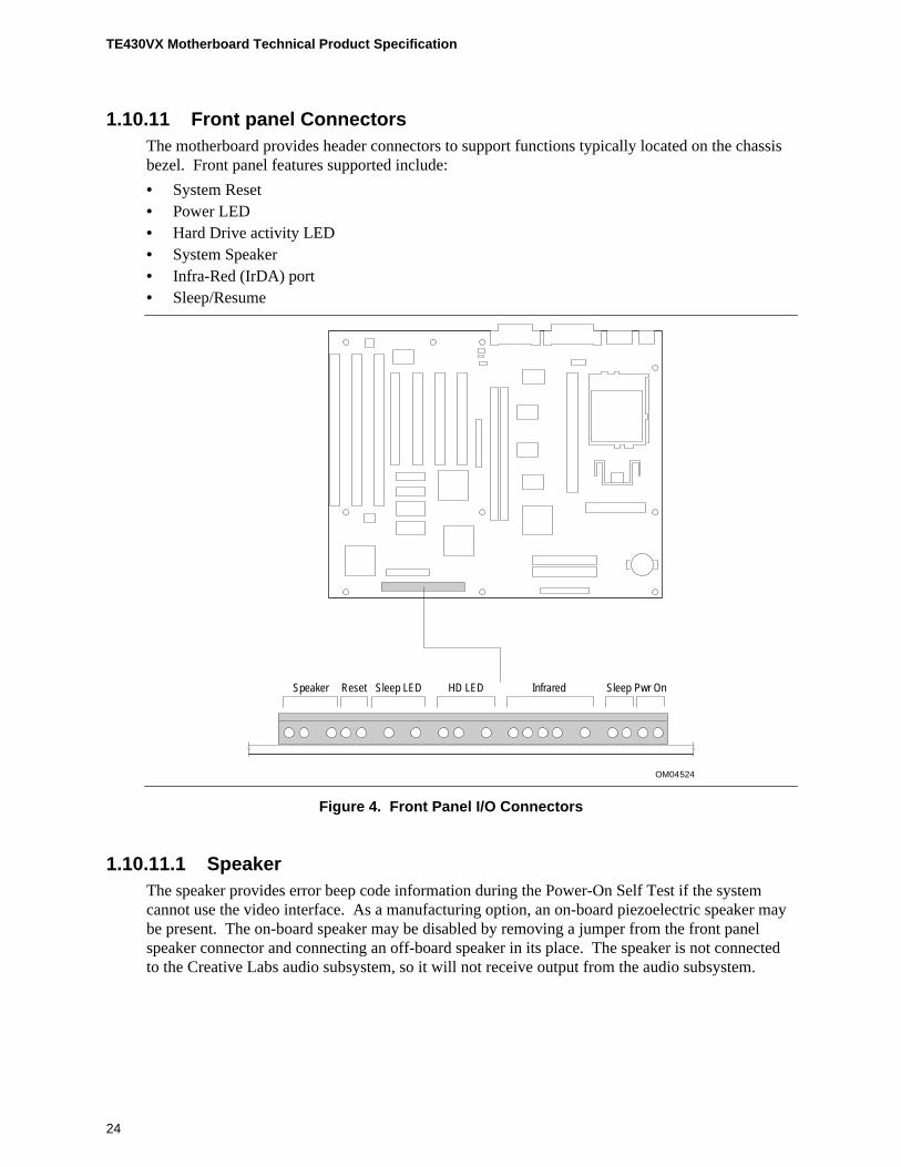
1.10.11 Front panel ConnectorsThe motherboard provides header connectors to support functions typically located on the chassisbezel. Front panel features supported include:
• System Reset• Power LED• Hard Drive activity LED• System Speaker• Infra-Red (IrDA) port• Sleep/Resume
OM04524
Speaker Reset Sleep LED HD LED Infrared Sleep Pwr On
Figure 4. Front Panel I/O Connectors
1.10.11.1 SpeakerThe speaker provides error beep code information during the Power-On Self Test if the systemcannot use the video interface. As a manufacturing option, an on-board piezoelectric speaker maybe present. The on-board speaker may be disabled by removing a jumper from the front panelspeaker connector and connecting an off-board speaker in its place. The speaker is not connectedto the Creative Labs audio subsystem, so it will not receive output from the audio subsystem.

Motherboard Description
25
1.10.11.2 ResetThis header can be connected to a momentary SPST type switch that is normally open. When theswitch is closed, the system will hard reset and run POST.
1.10.11.3 Sleep or Power LEDThis header can be connected to an LED to provide a light when the system is powered on. ThisLED will also blink when the system is in a power-managed state.
1.10.11.4 HD LEDThis header can be connected to an LED to provide a visual indicator for when an IDE hard driveconnected to the onboard IDE controller is being read or written.
1.10.11.5 Infra-Red (IrDA) connectorSerial port 2 can be configured to support an IrDA module via a 5 pin header connector . Onceconfigured for IrDA, the user can transfer files to or from portable devices such as laptops, PDA’sand printers using application software such as LapLink. The IrDA specification provides for datatransfers at 115 Kbps from a distance of 1 meter. A pin is also designated for hardware ConsumerIR support.
1.10.11.6 Sleep / resumeWhen Advanced Power Management (APM) is activated in the system BIOS and the OperatingSystem’s APM driver is loaded, Sleep mode (Stand-By) can be entered in one of three ways: anoptional front panel “Sleep/Resume” button, a user defined keyboard hot key, or prolonged systeminactivity. The Sleep/Resume button is supported by a 2-pin header (pins 3 and 4) located on thefront panel I/O connector (J9E2). Closing the “Sleep” switch will generate an SMI (SystemManagement Interrupt) to the processor which immediately goes into System Management Mode(SMM), the so called “Sleep” mode.
The front panel “Sleep” switch must be a momentary two pin SPST type that is normally open.The function of the Sleep/Resume button can also be achieved via a keyboard hot-key sequence, orby a time-out of the system inactivity timer. Both the keyboard hot-key and the inactivity timer areprogrammable in the BIOS setup (timer is set to 10 minutes by default). To re-activate the system,or “Resume”, the user must simply press the sleep/resume button again, or use the keyboard ormouse. Mouse activity will only “wake up” the system if a mouse driver is loaded. While thesystem is in “sleep” mode it is fully capable of responding to and servicing external interrupts(such as in-coming FAX) even though the monitor will only turn on if a user interrupt(keyboard/mouse) occurs as mentioned above

TE430VX Motherboard Technical Product Specification
26
1.10.11.7 Remote ON/OFF and Soft Power SupportFor power supplies that support the Remote ON/OFF feature, this 2 pin header (see Figure 4 pins1 and 2 of J9E2) should be connected to the system power ON/OFF switch. The power ON/OFFbutton should be a momentary SPST switch that is normally open. The power supply controlsignal (PS_ON) is supported via the primary power connector. Traditional power supplies withmechanical ON/OFF switches that do not support remote ON/OFF or “soft-off” will by-pass thiscircuit.
After turning the system ON by pushing the power ON/OFF button, the TE430VX motherboard(with a power supply that supports remote power on/off) can be turned OFF from one of twosources: the front panel power ON/OFF switch, or a “soft off” signal (coming from the Super I/Ocontroller) that can be controlled by the operating system. In “soft off”, an APM command issuedto the system BIOS will cause the power supply to turn OFF via the “PS ON” control signal on thepower connector. For example, Windows 95 will issue this APM command when the user clickson the Shutdown icon. Power can be restored by simply pressing the power ON/OFF switch atwhich time the system will power back up and run POST.
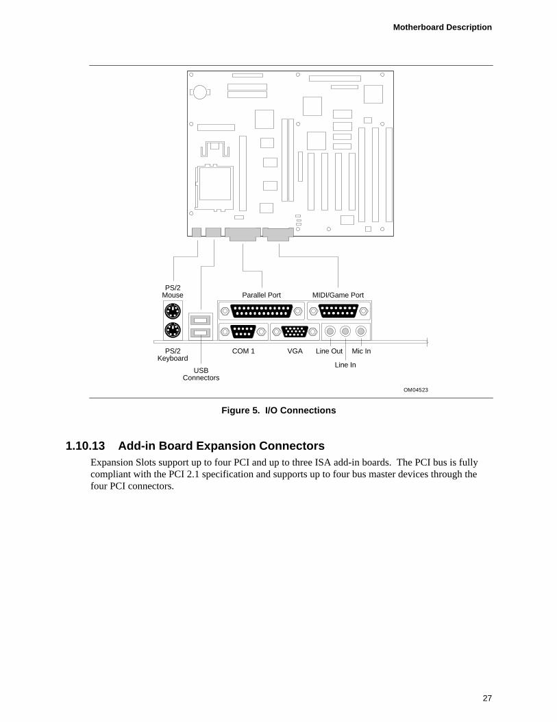
1.10.12 Back Panel ConnectorsThe back panel provides external access to PS/2 style keyboard and mouse connectors, two USBconnectors, one parallel port, one serial port, a VGA connector, a MIDI/game port, and the externalaudio jacks which are integrated on the motherboard. Figure 5 shows the general location of theI/O connectors.
Motherboard Description
27
OM04523
PS/2Keyboard
COM 1
MIDI/Game Port
Line Out
Line In
Mic InVGA
Parallel PortPS/2
Mouse
USBConnectors
Figure 5. I/O Connections
1.10.13 Add-in Board Expansion ConnectorsExpansion Slots support up to four PCI and up to three ISA add-in boards. The PCI bus is fullycompliant with the PCI 2.1 specification and supports up to four bus master devices through thefour PCI connectors.
TE430VX Motherboard Technical Product Specification
28
1.11 Jumper Settings
OM04525
J9C1
Pin-1
4 65
32
A B C D
1
J7A1
BiosRecoveryJumper
3
1
J6M1
VoltageRegulatorJumper
3
Configuration Jumper
Figure 6. Jumper Locations
Table 2. Configuration Jumper Settings
Function Jumper Configuration
Host Bus Speed(Note: These jumpers also set PCI andISA clock speeds .)
J9C1-C See Table 3
CPU Speed Ratio J9C1-D See Table 3
CMOS Clear J9C1-A 4-5 Keep (Default )5-6 Clear
Password Clear J9C1-A 1-2 Password Enabled (Default )2-3 Password Clear/Disabled
CMOS Setup Access J9C1-B * 1-2 Access Allowed (Default ) 2-3 Access Denied
Reserved J9C1-B Not jumpered
Motherboard Description
29
1.11.1 CPU Configuration (J9C1-C, D)These allow the motherboard to be switched between different speeds of the Pentium processor.These jumpers also affect the PCI and ISA clock speeds according to the following table.
Table 3. CPU/SYSTEM Speed Settings
CPU Freq. (MHz) Host Bus Freq. (MHz) J9C1-C dJ9C1-D
200 66 1-2,5-6 2-3,5-6
166 66 1-2,5-6 1-2,5-6
150 60 2-3,4-5 1-2,5-6
133 66 1-2,5-6 2-3,4-5
120 60 2-3,4-5 2-3,4-5
100 66 1-2,5-6 1-2,4-5
90 60 2-3,4-5 1-2,4-5
75 50 2-3,5-6 1-2,4-5
reserved - 2-3,5-6 2-3,5-6
reserved - 2-3,4-5 2-3,5-6
reserved - 1-2,4-5 1-2,4-5
reserved - 1-2,4-5 2-3,4-5
reserved - 1-2,4-5 1-2,5-6
1.11.2 Clear CMOS (J9C1-A, Pins 4,5,6)Allows CMOS settings to be reset to default values by moving the jumper from pins 4-5 to pins5-6 and turning the system on. When the system reports that “NVRAM cleared by jumper”, thesystem can be turned off, and the jumper should be returned to the 4-5 position to restore normaloperation. This procedure should be done whenever the system BIOS is updated. Default is forthis jumper to be on pins 4-5.
1.11.3 Password clear (J9C1-A, Pins 1,2,3)Allows system password to be cleared by moving the jumper from pins 1-2 to pins 2-3 and turningthe system on. The system should then be turned off and the jumper should be returned to the 3-5position to restore normal operation. This procedure should only be done if the user password hasbeen forgotten. The password function is effectively disabled if this jumper is in the 1-3 position.Default is for the password to be enabled (3-5 position).
1.11.4 CMOS Setup Access (J9C1-B, Pins 1,2,3)Allows access to CMOS Setup utility to be disabled by moving this jumper from the 1-2 positionto the 2-3 position. Default is for access to setup to be enabled (1-2 position).
TE430VX Motherboard Technical Product Specification
30
1.11.5 CPU Voltage (J6M1)This jumper block changes the output of the on-board voltage regulator. Pins 2-3 should bejumpered for processors that require standard voltage regulation, pins 1-2 should be jumpered forprocessors that require the VRE specification. This jumper should not be changed by the userunless changing to a new processor type. Some upgrade processors may require a different setting,check the processor's documentation for the correct setting. (Standard = 3.135-3.63V,VRE = 3.465-3.63V)
1.11.6 BIOS Recovery (J7A1)This jumper allows the BIOS to be recovered if it has been corrupted by moving the jumper fromthe 1-2 position to the 2-3 position and inserting a recovery diskette. Default setting is for normaloperation (1-2 position).
1.12 Reliability
The Mean-Time-Between-Failures (MTBF) data is calculated from predicted data @ 55C.
Motherboard 80,798 hours
1.13 Environmental
Table 4. Motherboard Environmental Specifications
Parameter Specification
TemperatureNon-OperatingOperating
-40oC to +70oC+0oC to +55oC
DC Voltage+5 V-5 V+12 V-12 V+3.3 V
±5 %±5 %±5 %±5 %±5 %
VibrationUnpackaged 5 Hz to 20 Hz : 0.01g² Hz sloping up to 0.02 g² Hz
20 Hz to 500 Hz : 0.02g² Hz (flat)
Packaged 10 Hz to 40 Hz : 0.015g² Hz (flat)40 Hz to 500 Hz : 0.015g² Hz sloping down to 0.00015 g² Hz
Motherboard Description
31
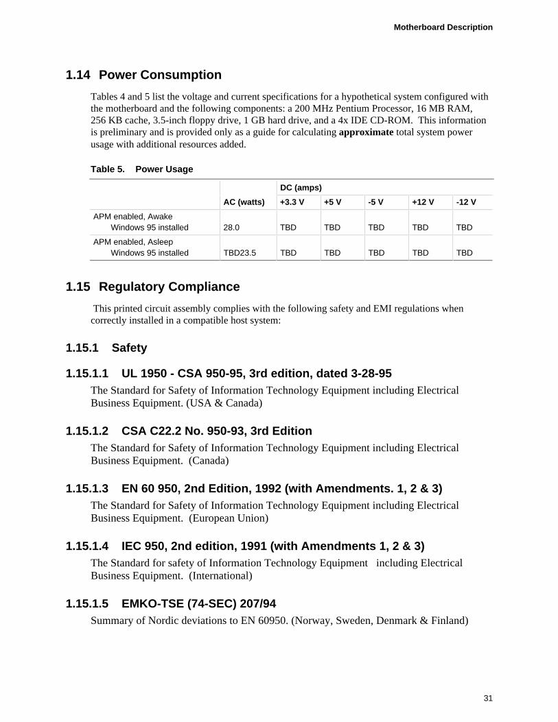
1.14 Power Consumption
Tables 4 and 5 list the voltage and current specifications for a hypothetical system configured withthe motherboard and the following components: a 200 MHz Pentium Processor, 16 MB RAM,256 KB cache, 3.5-inch floppy drive, 1 GB hard drive, and a 4x IDE CD-ROM. This informationis preliminary and is provided only as a guide for calculating approximate total system powerusage with additional resources added.
Table 5. Power Usage
DC (amps)
AC (watts) +3.3 V +5 V -5 V +12 V -12 V
APM enabled, AwakeWindows 95 installed 28.0 TBD TBD TBD TBD TBD
APM enabled, AsleepWindows 95 installed TBD23.5 TBD TBD TBD TBD TBD
1.15 Regulatory Compliance
This printed circuit assembly complies with the following safety and EMI regulations whencorrectly installed in a compatible host system:
1.15.1 Safety
1.15.1.1 UL 1950 - CSA 950-95, 3rd edition, dated 3-28-95The Standard for Safety of Information Technology Equipment including ElectricalBusiness Equipment. (USA & Canada)
1.15.1.2 CSA C22.2 No. 950-93, 3rd EditionThe Standard for Safety of Information Technology Equipment including ElectricalBusiness Equipment. (Canada)
1.15.1.3 EN 60 950, 2nd Edition, 1992 (with Amendments. 1, 2 & 3)The Standard for Safety of Information Technology Equipment including ElectricalBusiness Equipment. (European Union)
1.15.1.4 IEC 950, 2nd edition, 1991 (with Amendments 1, 2 & 3)The Standard for safety of Information Technology Equipment including ElectricalBusiness Equipment. (International)
1.15.1.5 EMKO-TSE (74-SEC) 207/94Summary of Nordic deviations to EN 60950. (Norway, Sweden, Denmark & Finland)
TE430VX Motherboard Technical Product Specification
32
1.15.2 EMI
1.15.2.1 CISPR 22, 2nd Edition, 1993Limits and methods of measurement of Radio Interference Characteristics of InformationTechnology Equipment. (International)
1.15.2.2 EN 55 022, 1995Limits and methods of measurement of Radio Interference Characteristics of InformationTechnology Equipment. (Europe)
1.15.2.3 EN 50 082-1 (1992)Generic Immunity Standard; Currently compliance is determined via testing to IEC 801-2, -3 and-4. (Europe)
1.15.2.4 VCCI Class 2 (ITE)Implementation Regulations for Voluntary Control of Radio Interference by Data ProcessingEquipment and Electronic Office Machines. (Japan)
1.15.2.5 FCC Class BThis equipment has been verified to be within the energy emission limits for Class B digitaldevices defined in the FCC Rules, Subpart B.
These limits are designed to provide reasonable protection against harmful interference in aresidential installation. This equipment generates and uses energy of about the same frequency asradio and TV signals. Installed correctly, it will not interfere with your radio and TV. However,we do not guarantee that is will not interfere.
For more information about interference, you can order the following booklet from the U.S.Government Printing Office, Washington, DC 20402. Ask for stock number 004-000-00345-4:“How to identify and Resolve Radio-TV interference Problems” (USA)
1.15.2.6 ICES-003, Issue 2Interference-Causing Equipment Standard, Digital Appartus. (Canada)
1.15.3 Product Certification Markings
1.15.3.1 European CE MarkingMarking on the board or shipping container.
1.15.3.2 UL RecognitionUL Recognized Marking consists of UL File No. E139761 on component side of board PB No. onsolder side of board. Board material flammability is 94V-1 or -0.
Motherboard Description
33
1.15.3.3 Canadian ComplianceMarking consists of small c followed by a stylized backward UR on component side of board.
1.15.4 Installation Requirements
CAUTIONTo avoid an adverse impact on the compliance with safety or regulatory requirements due toinstallation of this board assembly, the following guidelines must be followed.
1.15.4.1 Follow Installation InstructionsBe sure to read and adhere to all of these instructions, and the instructions supplied with the hostsystem and associated modules. If the instructions of the host system appear to be incompatiblewith these instructions or the instructions of any associated modules, contact the suppliers’technical support organizations for the products involved to determine the appropriate action forcontinued safety and regulatory compliance of the resultant system. Failure to read and followinstructions provided by host system and module suppliers may result in increased safety risk andnon-compliance with regional laws and regulations.
1.15.4.2 Assure Host System CompatibilityFor electromagnetic compatibility, the host system enclosure and power supply should have passedelectromagnetic compatibility testing using a board with a microprocessor from the same family asthe microprocessor on this board, operating at the same or higher microprocessor speed. Also,only peripherals (computer input/output devices, terminals, printers, etc.) that are CE Marked andcertified by the FCC to comply with Class B limits may be attached to this board. Pay particularattention to the installation instructions of the host system and other modules, particularlyconcerning certifications, external I/O cable shielding and filtering, mounting, grounding andbonding requirements to assure appropriate shielding effectiveness. Otherwise electromagneticcompatibility testing must be repeated on a representative sample of the complete system.
For safety, if mismating of connectors could result in a hazard, assure that all connectors aresufficiently keyed to prevent mismating.
1.15.4.3 Use Only In Intended ApplicationsThis product was evaluated for use in systems installed in offices, homes, schools, computer roomsor similar applications. Other applications, such as medical, industrial, alarm systems and testequipment may necessitate a re-evaluation of the product suitability.

TE430VX Motherboard Technical Product Specification
34
1.15.4.4 Assure Host System & Accessory CertificationsAssure that the host system, any other subassemblies such as board & drive assemblies beingadded in, and internal or external wiring, are properly certified for the region(s) the end-productwill be used in. Proof of certification can be determined by the marks on the product. Forexample:
EuropeThe CE Marking signifies compliance with all relevant EU requirements. If the host system doesnot bear the CE Marking, obtain a supplier’s Declaration of Conformity to the appropriatestandards required by the European EMC Directive and Low Voltage Directive. Other Directives,such as the Machinery and Telecommunications Directives, may also apply depending on the typeof product. No regulatory assessment is necessary for low voltage DC wiring used internally, orwiring used externally when provided with appropriate overcurrent protection. Appropriateprotection is achieved by max. 8 Amp current limiting circuit or a max. 5 Amp fuse or PositiveTemperature Coefficient Resistor (PTC). All Intel motherboards presently have PTC’s on allexternal ports which provide DC power externally.
U.S.For safety, a certification mark by a Nationally Recognized Testing Laboratory (NRTL) such asUL, CSA or ETL. External wiring must be UL Listed and suitable for the use. Internal wiringmust be UL Listed or Recognized and rated appropriately for the voltages and temperaturesinvolved. For electromagnetic interference, the FCC mark: Class A for commercial or industrialonly; or Class B for all applications other than described in Item 1.14.3.3 above.
CanadaFor safety, a nationally recognized certification mark such as CSA or cUL. No regulatoryassessment is necessary for low voltage DC wiring used internally, or wiring used externally whenprovided with appropriate overcurrent protection. Appropriate protection is achieved by max.8 Amp current limiting circuit or a max. 5 Amp fuse or Positive Temperature Coefficient Resistor(PTC). All Intel motherboards presently have PTC’s on all external ports which provide DC powerexternally.
1.15.4.5 Installation PrecautionsDuring installation and initial test, use caution to avoid personal injury and damage to wiring dueto sharp pins on connectors and printed circuit assemblies, rough chassis edges and corners, andhot components. Adhere to warnings and limitations regarding accessibility into areas designatedonly for authorized technical personnel.
Motherboard Description
35
1.15.4.6 Battery MarkingThere is insufficient space on this board product to provide the required replacement and disposalinstructions for the battery. The following marking must be placed permanently and legibly on thehost system as near as possible to the battery:
CAUTIONDanger of explosion if battery is incorrectly replaced
Replace with only the same or equivalent type recommended by the manufacturer. Dispose of usedbatteries according to the manufacturer’s instructions.
1.15.4.7 Overload Protection:Unless the power supply is provided with inherent overcurrent protection, use caution to avoidoverloading the power supply output. This can be accomplished by assuring that the calculatedtotal current load of all the modules within the system is less than the output current rating of thepower supply. Failure to accomplish this could result in overheating in the power supply, whichcould result in a fire or could cause damage to insulation separating hazardous AC line circuitryfrom low-voltage user accessible circuitry. If the load drawn by a particular module cannot bedetermined by the markings and instructions supplied with the module, contact the modulesupplier’s technical support organization.

37
2 Motherboard Resources
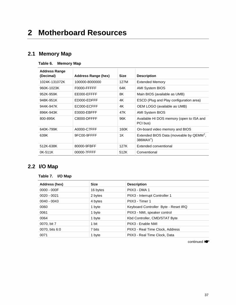
2.1 Memory Map
Table 6. Memory Map
Address Range(Decimal) Address Range (hex) Size Description
1024K-131072K 100000-8000000 127M Extended Memory
960K-1023K F0000-FFFFF 64K AMI System BIOS
952K-959K EE000-EFFFF 8K Main BIOS (available as UMB)
948K-951K ED000-EDFFF 4K ESCD (Plug and Play configuration area)
944K-947K EC000-ECFFF 4K OEM LOGO (available as UMB)
896K-943K E0000-EBFFF 47K AMI System BIOS
800-895K C8000-DFFFF 96K Available HI DOS memory (open to ISA andPCI bus)
640K-799K A0000-C7FFF 160K On-board video memory and BIOS
639K 9FC00-9FFFF 1K Extended BIOS Data (moveable by QEMM†,386MAX†)
512K-638K 80000-9FBFF 127K Extended conventional
0K-511K 00000-7FFFF 512K Conventional
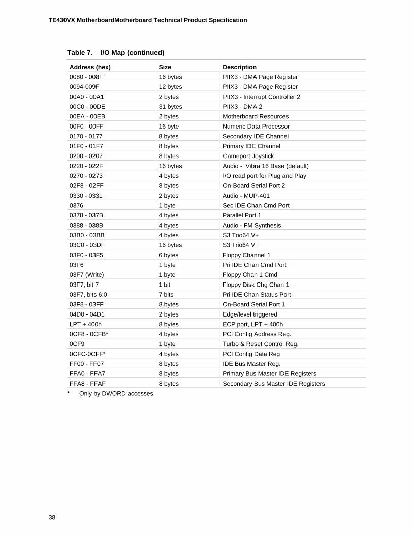
2.2 I/O Map
Table 7. I/O Map
Address (hex) Size Description
0000 - 000F 16 bytes PIIX3 - DMA 1
0020 - 0021 2 bytes PIIX3 - Interrupt Controller 1
0040 - 0043 4 bytes PIIX3 - Timer 1
0060 1 byte Keyboard Controller Byte - Reset IRQ
0061 1 byte PIIX3 - NMI, speaker control
0064 1 byte Kbd Controller, CMD/STAT Byte
0070, bit 7 1 bit PIIX3 - Enable NMI
0070, bits 6:0 7 bits PIIX3 - Real Time Clock, Address
0071 1 byte PIIX3 - Real Time Clock, Data
continued ☛
TE430VX MotherboardMotherboard Technical Product Specification
38
Table 7. I/O Map (continued)
Address (hex) Size Description
0080 - 008F 16 bytes PIIX3 - DMA Page Register
0094-009F 12 bytes PIIX3 - DMA Page Register
00A0 - 00A1 2 bytes PIIX3 - Interrupt Controller 2
00C0 - 00DE 31 bytes PIIX3 - DMA 2
00EA - 00EB 2 bytes Motherboard Resources
00F0 - 00FF 16 byte Numeric Data Processor
0170 - 0177 8 bytes Secondary IDE Channel
01F0 - 01F7 8 bytes Primary IDE Channel
0200 - 0207 8 bytes Gameport Joystick
0220 - 022F 16 bytes Audio - Vibra 16 Base (default)
0270 - 0273 4 bytes I/O read port for Plug and Play
02F8 - 02FF 8 bytes On-Board Serial Port 2
0330 - 0331 2 bytes Audio - MUP-401
0376 1 byte Sec IDE Chan Cmd Port
0378 - 037B 4 bytes Parallel Port 1
0388 - 038B 4 bytes Audio - FM Synthesis
03B0 - 03BB 4 bytes S3 Trio64 V+
03C0 - 03DF 16 bytes S3 Trio64 V+
03F0 - 03F5 6 bytes Floppy Channel 1
03F6 1 byte Pri IDE Chan Cmd Port
03F7 (Write) 1 byte Floppy Chan 1 Cmd
03F7, bit 7 1 bit Floppy Disk Chg Chan 1
03F7, bits 6:0 7 bits Pri IDE Chan Status Port
03F8 - 03FF 8 bytes On-Board Serial Port 1
04D0 - 04D1 2 bytes Edge/level triggered
LPT + 400h 8 bytes ECP port, LPT + 400h
0CF8 - 0CFB* 4 bytes PCI Config Address Reg.
0CF9 1 byte Turbo & Reset Control Reg.
0CFC-0CFF* 4 bytes PCI Config Data Reg
FF00 - FF07 8 bytes IDE Bus Master Reg.
FFA0 - FFA7 8 bytes Primary Bus Master IDE Registers
FFA8 - FFAF 8 bytes Secondary Bus Master IDE Registers
* Only by DWORD accesses.
Motherboard Resources
39
2.3 Soft-Off Control
The motherboard design supports Soft-off control via the SMM code in the BIOS
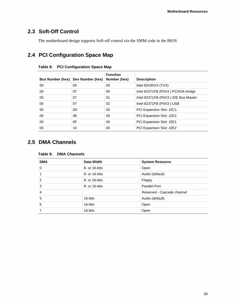
2.4 PCI Configuration Space Map
Table 8. PCI Configuration Space Map
Bus Number (hex) Dev Number (hex)FunctionNumber (hex) Description
00 00 00 Intel 82430VX (TVX)
00 07 00 Intel 82371FB (PIIX3 ) PCI/ISA bridge
00 07 01 Intel 82371FB (PIIX3 ) IDE Bus Master
00 07 02 Intel 82371FB (PIIX3 ) USB
00 0D 00 PCI Expansion Slot: J2C1
00 0E 00 PCI Expansion Slot: J2D1
00 0F 00 PCI Expansion Slot: J2E1
00 10 00 PCI Expansion Slot: J2E2
2.5 DMA Channels
Table 9. DMA Channels
DMA Data Width System Resource
0 8- or 16-bits Open
1 8- or 16-bits Audio (default)
2 8- or 16-bits Floppy
3 8- or 16-bits Parallel Port
4 Reserved - Cascade channel
5 16-bits Audio (default)
6 16-bits Open
7 16-bits Open
TE430VX MotherboardMotherboard Technical Product Specification
40
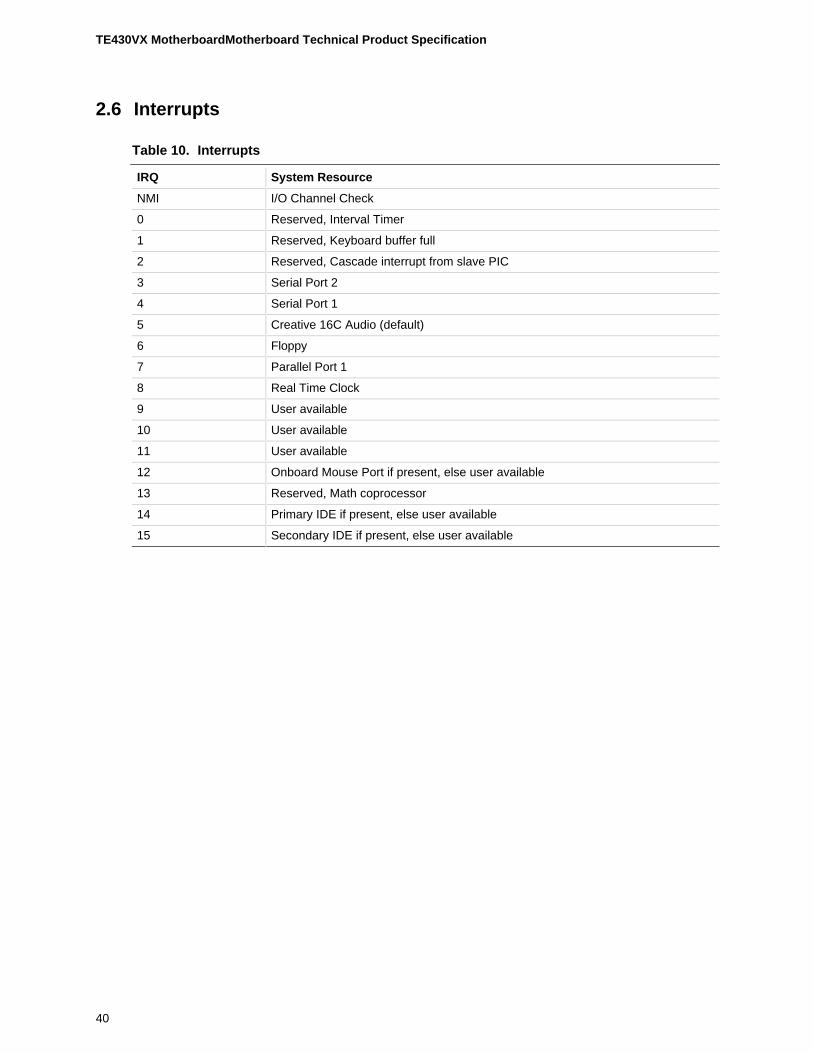
2.6 Interrupts
Table 10. Interrupts
IRQ System Resource
NMI I/O Channel Check
0 Reserved, Interval Timer
1 Reserved, Keyboard buffer full
2 Reserved, Cascade interrupt from slave PIC
3 Serial Port 2
4 Serial Port 1
5 Creative 16C Audio (default)
6 Floppy
7 Parallel Port 1
8 Real Time Clock
9 User available
10 User available
11 User available
12 Onboard Mouse Port if present, else user available
13 Reserved, Math coprocessor
14 Primary IDE if present, else user available
15 Secondary IDE if present, else user available
41
3 Motherboard BIOS and Setup Utility
3.1 Introduction
The motherboard uses an Intel BIOS, which is stored in Flash EEPROM and upgraded using afloppy disk-based program. In addition to the Intel BIOS, the Flash EEPROM also contains theSetup utility, Power-On Self Tests (POST), APM 1.1, the PCI auto-configuration utility, andWindows 95 ready Plug and Play. This motherboard also supports system BIOS shadowing,allowing the BIOS to execute from 64-bit on-board write-protected DRAM.
Hardware has been added to the board so only Intel compiled BIOS can be flashed into the FlashEEPROM. This was done for extended virus protection.
The BIOS displays a sign-on message during POST identifying the type of BIOS and a five-digitrevision code. The initial production BIOS in the motherboard will be identified as 1.00.0x.CY0.
Information on BIOS functions can be found in the IBM† PS/2 and Personal Computer BIOSTechnical Reference published by IBM, and the ISA and EISA Hi-Flex AMIBIOS TechnicalReference published by AMI. Both manuals are available at most technical bookstores
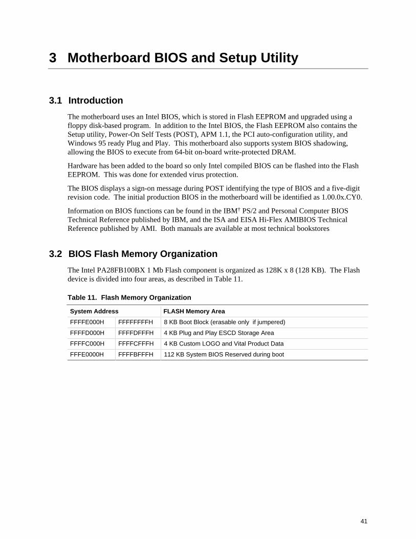
3.2 BIOS Flash Memory Organization
The Intel PA28FB100BX 1 Mb Flash component is organized as 128K x 8 (128 KB). The Flashdevice is divided into four areas, as described in Table 11.
Table 11. Flash Memory Organization
System Address FLASH Memory Area
FFFFE000H FFFFFFFFH 8 KB Boot Block (erasable only if jumpered)
FFFFD000H FFFFDFFFH 4 KB Plug and Play ESCD Storage Area
FFFFC000H FFFFCFFFH 4 KB Custom LOGO and Vital Product Data
FFFE0000H FFFFBFFFH 112 KB System BIOS Reserved during boot
TE430VX MotherboardMotherboard Technical Product Specification
42
3.3 BIOS Upgrades
Flash memory makes distributing BIOS upgrades easy. A new version of the BIOS can beinstalled from a diskette. BIOS upgrades are available to be down loaded from the secure sectionon the Intel bulletin board, or Intel’s FTP site.
The disk-based Flash upgrade utility, FMUP.EXE, has three options for BIOS upgrades:
• The Flash BIOS can be updated from a file on a disk;• The current BIOS code can be copied from the Flash EEPROM to a disk file as a backup in the
event that an upgrade cannot be successfully completed; or• The BIOS in the Flash device can be compared with a file to ensure the system has the correct
version.
The upgrade utility ensures the upgrade BIOS extension matches the target system to preventaccidentally installing a BIOS for a different type of system.
3.4 PCI IDE Support
The two local bus IDE connectors with independent I/O channel support are setup up automaticallyby the BIOS if the user selects “Autoconfiguration” in setup. The IDE interface supports PIOMode 3, and Mode 4 hard drives and recognition of ATAPI CD-ROMs, tape drives, and any otherATAPI devices. The BIOS will determine the capabilities of each drive and configure them tooptimize capacity and performance. For the high capacity hard drives typically available today, thedrive will be automatically be configured for Logical Block Addressing (LBA) for maximumcapacity and to PIO Mode 3 or 4 depending on the capability of the drive. The user is able tooverride the auto-configuration options by using the manual mode setting. The ATAPISpecification Revision 2.5 recommends that an ATAPI device be configured as shown in the tablebelow.
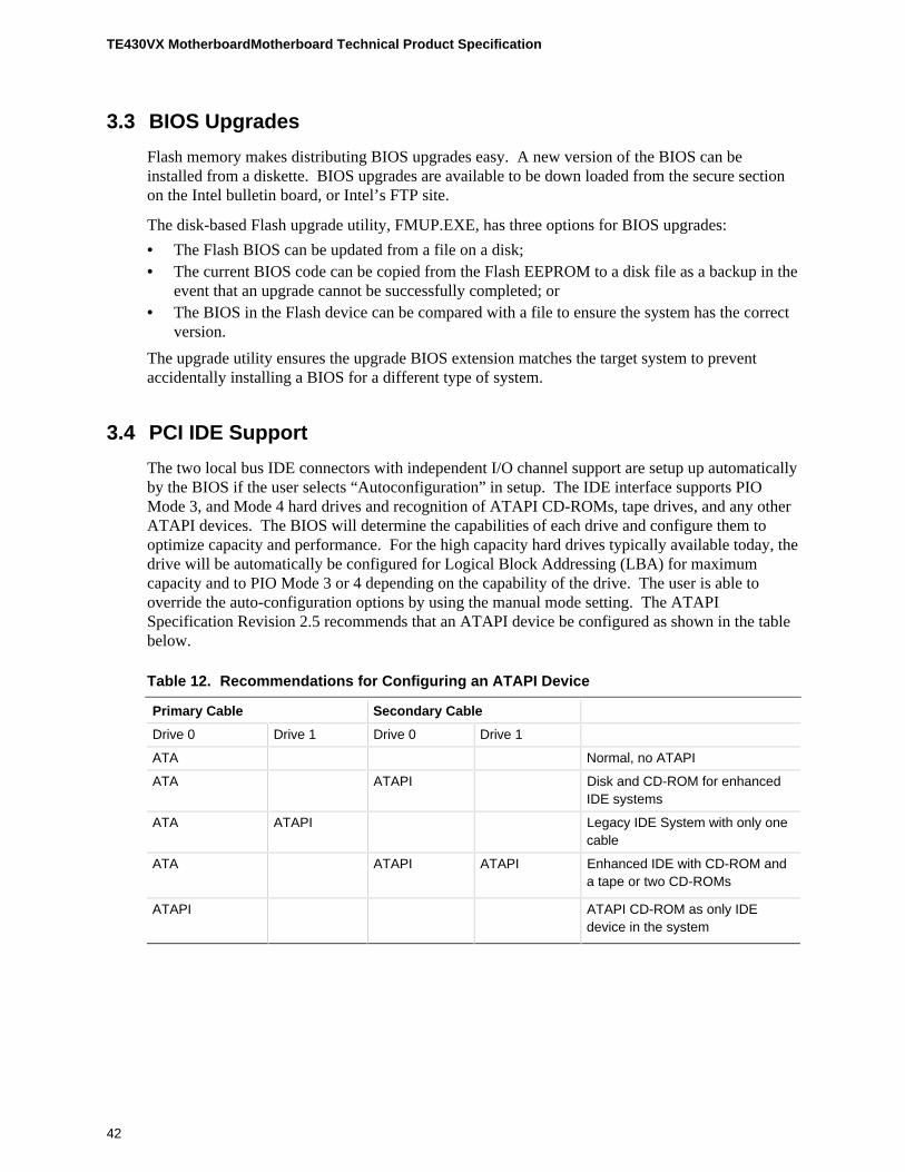
Table 12. Recommendations for Configuring an ATAPI Device
Primary Cable Secondary Cable
Drive 0 Drive 1 Drive 0 Drive 1
ATA Normal, no ATAPI
ATA ATAPI Disk and CD-ROM for enhancedIDE systems
ATA ATAPI Legacy IDE System with only onecable
ATA ATAPI ATAPI Enhanced IDE with CD-ROM anda tape or two CD-ROMs
ATAPI ATAPI CD-ROM as only IDEdevice in the system
Motherboard BIOS and Setup Utility
43
3.5 PCI Auto-configuration
The PCI auto-configuration utility operates in conjunction with the system Setup utility to allowthe insertion and removal of PCI cards to the system without user intervention (Plug and Play).When the system is turned on after adding a PCI add-in card, the BIOS automatically configuresinterrupts, I/O space, and other parameters. PCI interrupts are distributed to available ISAinterrupts that have been not been assigned to an ISA card, or system resources. Those interruptsleft set to “available” in the CMOS setup will be considered free for PCI add-in card use. It isnondeterministic as to which PCI interrupt will be assigned to which ISA IRQ.
The PCI Auto-Configuration function complies with version 2.10 of the PCI BIOS specification.System configuration information is stored in ESCD format. The ESCD data may be cleared bysetting the CMOS clear jumper to the ON position.
PCI specification 2.1 for add-in card auto-configuration is also a part of the Plug and Play BIOS.Peer-to-peer hierarchical PCI Bridge 1.0 is supported, and by using an OEM supplied option ROMor TSR, a PCI-to-PCMCIA bridge capability is possible as well.
3.6 ISA Plug and Play
The BIOS incorporates ISA Plug and Play capabilities as delivered by Plug and Play Release 1.0A(Plug and Play BIOS V.. 1.0A, ESCD V.. 1.03). When used in conjunction with the ISAConfiguration Utility (ICU) for DOS or Windows 3.x, the system allows auto-configuration ofPlug and Play ISA cards, PCI cards, and resource management for legacy ISA cards. Because theBIOS supports configuring devices across PCI bridges, release 1.41 or greater of the ICU must beused with the motherboard to properly view and change system settings. System configurationinformation is stored in ESCD format. The ESCD data may be cleared by setting the CMOS clearjumper to the ON position.
The BIOS also has a setup option to support the Windows 95 run time Plug and Play utilities.When this option is selected, only devices critical to booting are assigned resources by the BIOS.Device Node information is available for all devices to ensure compatibility with Windows 95.
Copies of the IAL Plug and Play specification may be obtained via the Intel BBS , or viaCompuServe† by typing Go PlugPlay.
TE430VX MotherboardMotherboard Technical Product Specification
44
3.7 Advanced Power Management
The BIOS has support for Advanced Power Management (APM version 1.1). The energy savingStand By mode can be initiated by a keyboard hot key sequence set by the user, a time-out periodset by the user, or by a suspend/resume button tied to the front panel sleep connector.
When in Stand-by mode, the motherboard reduces power consumption by utilizing the Pentiumprocessor’s System Management Mode (SMM) capabilities and also spinning down hard drivesand turning off VESA DPMS compliant monitors. The user may select which DPMS mode (StandBy, Suspend, or Off) send to the monitor in setup. The ability to respond to external interrupts isfully maintained while in Stand-by mode allowing the system to service requests such as in-comingFax's or network messages while unattended. Any keyboard or mouse activity brings the systemout of the energy saving Stand By mode. When this occurs the monitor and IDE drives are turnedback on immediately.
APM is enabled in BIOS by default, however, the system must be configured with an APM driverin order for the system power saving features to take effect. Windows 95 will enable APMautomatically upon detecting the presence of the APM BIOS.
3.8 Language Support
The BIOS setup screen and help messages are supported in 32 languages. There are 5 languagestranslated at this time for use; American English, German, Italian, French, and Spanish.Translations of other languages will available at a later date.
With a 1 Mb Flash BIOS, only one language can be resident at a time. The default language isAmerican English, and will always be present unless another language is programmed into theBIOS using the Flash Language Update Program (FLUP) available on the Intel BBS.
3.9 Boot Options
Booting from CD-ROM is supported in adherence to the “El Torito” bootable CD-ROM formatspecification developed by Phoenix Technologies and IBM. Under the Boot Options field in setup,CD-ROM is one of four possible boot devices which are defined in priority order. The defaultsetting is for floppy to be the primary boot device and hard drive to be the secondary boot device.If CD-ROM is selected, it must be the first device. The third and fourth devices are set to disabledin the default configuration.. The user can add also select network as a boot device. The networkoption allows booting from a network add-in card with a remote boot ROM installed.
✏ NOTE
A copy of “El Torito” is available on Phoenix Web page (http://www.ptltd.com/techs/specs.html).

Motherboard BIOS and Setup Utility
45
3.10 Flash LOGO Area
The motherboard supports a 4 KB programmable FLASH user area located at EC000-ECFFF. AnOEM may use this area to display a custom logo. The BIOS accesses the user area just aftercompleting POST. A utility is available from Intel to assist with installing a logo into flash fordisplay during POST. Contact your local Intel Sales office or authorized distributor for furtherinformation.
3.11 Setup Enable Jumper
A motherboard configuration jumper controls access to the BIOS Setup utility. By setting thejumper to the disable position, the user is prevented from accessing the Setup utility during thePower-on Self Test or at any other time. The message prompting the user to press <F1> to entersetup is also disabled.
3.12 BIOS Setup Program
The ROM-based Setup utility allows the configuration to be modified without opening the systemfor most basic changes. The Setup utility is accessible only during the Power-On Self Test (POST)by pressing the <F1> key after the POST memory test has begun and before boot begins. Aprompt may be enabled that informs users to press the <F1> key to access Setup. A jumper settingon the motherboard can be set to prevent user access to Setup for security purposes.
3.12.1 Overview of the Setup Menu ScreensThe Setup program initially displays the Main menu screen. In each screen there are options formodifying the system configuration. Select a menu screen by pressing the left <←> or right <→>arrow keys. Use the up <↑> or down <↓> arrow keys to select items in a screen. Use the <Enter>key to select an item for modification. For certain items, pressing <Enter> will bring up asubscreen. After you have selected an item, use the arrow keys to modify the setting.
TE430VX MotherboardMotherboard Technical Product Specification
46
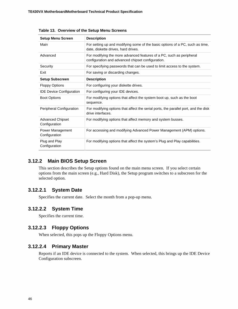
Table 13. Overview of the Setup Menu Screens
Setup Menu Screen Description
Main For setting up and modifying some of the basic options of a PC, such as time,date, diskette drives, hard drives.
Advanced For modifying the more advanced features of a PC, such as peripheralconfiguration and advanced chipset configuration.
Security For specifying passwords that can be used to limit access to the system.
Exit For saving or discarding changes.
Setup Subscreen Description
Floppy Options For configuring your diskette drives.
IDE Device Configuration For configuring your IDE devices.
Boot Options For modifying options that affect the system boot up, such as the bootsequence.
Peripheral Configuration For modifying options that affect the serial ports, the parallel port, and the diskdrive interfaces.
Advanced ChipsetConfiguration
For modifying options that affect memory and system busses.
Power ManagementConfiguration
For accessing and modifying Advanced Power Management (APM) options.
Plug and PlayConfiguration
For modifying options that affect the system’s Plug and Play capabilities.
3.12.2 Main BIOS Setup ScreenThis section describes the Setup options found on the main menu screen. If you select certainoptions from the main screen (e.g., Hard Disk), the Setup program switches to a subscreen for theselected option.
3.12.2.1 System DateSpecifies the current date. Select the month from a pop-up menu.
3.12.2.2 System TimeSpecifies the current time.
3.12.2.3 Floppy OptionsWhen selected, this pops up the Floppy Options menu.
3.12.2.4 Primary MasterReports if an IDE device is connected to the system. When selected, this brings up the IDE DeviceConfiguration subscreen.
Motherboard BIOS and Setup Utility
47
3.12.2.5 Primary SlaveReports if an IDE device is connected to the system. When selected, this brings up the IDE DeviceConfiguration subscreen.
3.12.2.6 Secondary MasterReports if an IDE device is connected to the system. When selected, this brings up the IDE DeviceConfiguration subscreen.
3.12.2.7 Secondary SlaveReports if an IDE device is connected to the system. When selected, this brings up the IDE DeviceConfiguration subscreen.
3.12.2.8 LanguageSpecifies the language of the text strings used in the Setup program and the BIOS. The options areany installed languages.
3.12.2.9 Boot OptionsWhen selected, this brings up the Boot Options subscreen.
3.12.2.10 Video ModeReports the video mode. There are no options.
3.12.2.11 MouseReports if a mouse is installed or not. There are no options.
3.12.2.12 Base MemoryReports the amount of base memory. There are no options.
3.12.2.13 Extended MemoryReports the amount of extended memory. There are no options.
3.12.3 Floppy Options Subscreen
3.12.3.1 Floppy A:Reports if a diskette drive is connected to the system. There are no options.
3.12.3.2 Floppy B:Reports if a second diskette drive is connected to the system. There are no options.
TE430VX MotherboardMotherboard Technical Product Specification
48
3.12.3.3 Floppy A: TypeSpecifies the physical size and capacity of the diskette drive. The options are Disabled, 360 KB,5.25-inch; 1.2 MB, 5.25-inch; 720 KB, 3.5-inch; 1.44/1.25 MB, 3.5-inch; 2.88 MB, 3.5-inch. Thedefault is 1.44/1.25 MB, 3.5-inch.
3.12.3.4 Floppy B: TypeSpecifies the physical size and capacity of the diskette drive. The options are Disabled, 360 KB,5.25-inch; 1.2 MB, 5.25-inch; 720 KB, 3.5-inch; 1.44/1.25 MB, 3.5-inch; 2.88 MB, 3.5-inch. Thedefault is Disabled.
3.12.3.5 Floppy AccessSpecifies read/write access for all attached floppy drives. The options are Read/Write and ReadOnly. The default is Read/Write.
3.12.4 IDE Device Configuration Subscreen
3.12.4.1 IDE Device ConfigurationUsed to manually configure the hard drive or have the system auto configure it. The options areAuto Configured, User Definable and Disabled. The default is Auto Configured. If you selectUser Definable then the Number of Cylinders, Number of Heads, and Number of Sectors items canbe modified.
3.12.4.2 Number of CylindersIf IDE Device Configuration is set to User Definable, you must type the correct number ofcylinders for your hard disk. If Hard Disk Type is set to Auto Configured, this reports the numberof cylinders for your hard disk and cannot be modified.
3.12.4.3 Number of HeadsIf IDE Device Configuration is set to User Definable, you must type the correct number of headsfor your hard disk. If Hard Disk Type is set to Auto Configured, this reports the number of headsfor your hard disk and cannot be modified.
3.12.4.4 Number of SectorsIf IDE Device Configuration is set to User Definable, you must type the correct number of sectorsfor your hard disk. If Hard Disk Type is set to Auto Configured, this reports the number of sectorsfor your hard disk and cannot be modified.
3.12.4.5 Maximum CapacityReports the maximum capacity of your IDE Device. It is calculated from the number of cylinders,heads, and sectors. There are no options here.
Motherboard BIOS and Setup Utility
49
3.12.4.6 IDE Translation ModeSpecifies the IDE translation mode. The options are Standard CHS (standard cylinder head sector−less than 1024 cylinders), Logical Block, Extended CHS (extended cylinder head sector−greaterthan 1024 cylinders), and Auto Detected (BIOS detects IDE drive support for LBA). The default isAuto Detected.
CAUTIONDo not change this from the option selected when the hard drive was formatted. Changing theoption can result in corrupted data.
3.12.4.7 Multiple Sector SettingSets the number of sectors transferred by an IDE drive per interrupt generated. The options areDisabled, 4 Sectors/Block, 8 Sectors/Block, or Auto Detected. The default is Auto Detected.Check the specifications for your hard disk drive to determine which setting provides optimumperformance for your drive.
3.12.4.8 Fast Programmed I/O ModesSets how fast transfers on the IDE interface occur. The options are Disabled or Auto Detected.The default is Auto Detected. If set to Disabled, transfers occur at a less than optimized speed. Ifset to Auto Detected, transfers occur at the drive's maximum speed.
3.12.5 Boot Options SubscreenThis section describes the options available on the Boot Options subscreen.
3.12.5.1 First, Second, Third, Fourth Boot DeviceSets which drives the system checks to find an operating system to boot from. The followingoptions are available:
First Boot Device: Select Disabled, Floppy, Hard Disk, CD-ROM, Network.
Second, Third, Fourth Device: Select Disabled, Floppy, Hard Disk, Network.
3.12.5.2 System CacheEnables or disables both the primary and the secondary cache memory. The options are Enabled orDisabled. The default is Enabled.
3.12.5.3 Boot SpeedSets the system’s boot speed. The options are Deturbo and Turbo. The default is Turbo. If Turbois selected, boot-up occurs at full speed. If Deturbo is selected, the board operates at a slowerspeed.
TE430VX MotherboardMotherboard Technical Product Specification
50
3.12.5.4 Num LockSets the beginning state of the Num Lock feature on your keyboard. The options are On and Off.The default is Off.
3.12.5.5 Setup PromptTurns on (or off) the “Press <F1> Key if you want to run Setup” prompt during the power-upsequence. The options are Enabled and Disabled. The default is Enabled.
✏ NOTE
This option has no effect on your ability to access the Setup program. It only toggles the prompt.
3.12.5.6 Typematic Rate ProgrammingSets the typematic rates. The options are Default and Override. The default is Default. ChoosingOverride enables Typematic Rate Delay and Typematic Rate.
3.12.5.7 Typematic Rate DelaySets how long it takes for the key-repeat function to start when you hold down a key on thekeyboard. The options are 250, 500, 750, and 1000 millisecond delays. The default is 250. IfTypematic Rate Programming is set to Default, this option will not be visible.
3.12.5.8 Typematic RateSets the speed at which characters repeat when you hold down a key on the keyboard. The higherthe number, the faster the characters repeat. The options are 6, 8, 10, 12, 15, 20, 24, and 30characters per second. The default is 6. If Typematic Rate Programming is set to Default, thisoption will not be visible.
3.12.6 Advanced ScreenThis section describes the Setup options found on the Advanced menu screen. If you select certainoptions from the Advanced screen (e.g., Peripheral Configuration), the Setup program switches to asubscreen for the selected option. Subscreens are described in the sections following thedescription of the Advanced screen options.
3.12.6.1 Processor TypeReports the CPU type. There are no options.
3.12.6.2 Processor SpeedReports the CPU clock speed. There are no options.
3.12.6.3 Cache SizeReports the size of the secondary cache. There are no options. If your system contains no L2cache, this item will not appear.
Motherboard BIOS and Setup Utility
51
3.12.6.4 Peripheral ConfigurationWhen selected, this brings up the Peripheral Configuration subscreen.
3.12.6.5 Advanced Chipset ConfigurationWhen selected, this brings up the Advanced Chipset Configuration subscreen.
3.12.6.6 Power Management ConfigurationWhen selected and enabled, this brings up the Advanced Power Management subscreen.
3.12.6.7 Plug and Play ConfigurationWhen selected, this brings up the Plug and Play Configuration subscreen.
3.12.7 Peripheral Configuration SubscreenThis section describes the screens for the peripheral configuration subscreen.
3.12.7.1 Configuration ModeEnables you to choose between setting the peripheral configuration yourself, or having the systemdo it. The options are Auto and Manual. The default is Auto.
When Auto is selected, the system peripherals are automatically configured during power up. Theoptions below for PCI IDE Interface, Floppy Interface, Serial Port 1 and Serial Port 2 Addresses,Serial Port 2 IR Mode, and the Parallel Port Address cannot be modified. The settings displayedfor those options reflect the current state of the hardware.
3.12.7.2 PCI IDE InterfaceEnables or disables the PCI IDE hard disk interface. The options are Enabled and Disabled. Thedefault is Enabled. (If Configuration Mode is set to Auto, this option cannot be modified.)
3.12.7.3 Floppy InterfaceEnables or disables the diskette drive interface. The options are Enabled and Disabled. Thedefault is Enabled. (If Configuration Mode is set to Auto, this option cannot be modified.)
3.12.7.4 Serial Port 1 AddressSelects the address of the serial port. The options are Disabled; COM1, 3F8h; COM2, 2F8h;COM3, 3E8h; and COM4, 2E8h. The default is COM1, 3F8h. If the Configuration Mode is set toAuto, the Setup program assigns the first free COM port (normally COM1, 3F8h) as the serial port1 address, regardless of what is selected under the Serial Port 1 Address option. (If ConfigurationMode is set to Auto, this option cannot be modified.)
3.12.7.5 Serial Port 2 AddressSelects the address of the serial port. The options are Disabled; COM1, 3F8h; COM2, 2F8h;COM3, 3E8h; and COM4, 2E8h. The default is COM2, 2F8h. If the Configuration Mode is set to
TE430VX MotherboardMotherboard Technical Product Specification
52
Auto, the Setup program assigns the first free COM port (normally COM2, 2F8h) as the serial port2 address, regardless of what is selected under the Serial Port 2 Address option. (If ConfigurationMode is set to Auto, this option cannot be modified.)
✏ NOTE
If either serial port address is set, the address it is set to will not appear in the options dialog boxof the other serial port. If an ATI† mach32† or an ATI mach64† video controller is active, theCOM4, 2E8h address will not appear in the options dialog box of either serial port.
3.12.7.6 Serial Port 2 IR ModeMakes Serial Port 2 available to infrared applications. The options are Enabled and Disabled. Thedefault is Disabled. (If Configuration Mode is set to Auto, this option cannot be modified.)
3.12.7.7 Parallel Port AddressSelects the address and IRQ of the parallel port. The options are Disabled; LPT3, 3BCh, IRQ7;LPT1, 378h, IRQ7; LPT1, 378h, IRQ5; and LPT2, 278h, IRQ5. The default is LPT1, 378h, IRQ7.If the Configuration Mode is set to Auto, the setup program assigns LPT1, 378h, IRQ7 as theparallel port address, regardless of what is selected under the Parallel Port Address option. (IfConfiguration Mode is set to Auto, this option cannot be modified.)
3.12.7.8 Parallel Port ModeSelects the mode for the parallel port. The options are Compatible, Bi-directional, EPP, and ECP.The default is Compatible. Compatible means the parallel port operates in AT-compatible mode.Bi-directional means the parallel port operates in bi-directional PS/2-compatible mode. EPP andECP mean the parallel port operates high-speed, bi-directionally. This option is not affected by theConfiguration Mode field above.
3.12.8 Advanced Chipset Configuration SubscreenThis section describes the options available on the Advanced Chipset Configuration Subscreen.
3.12.8.1 Base Memory SizeSets the size of the base memory. The options are 512 KB and 640 KB. The default is 640 KB.
3.12.8.2 ISA LFB SizeSets the size of the linear frame buffer. The options are Disabled and 1 MB. The default isDisabled. If this is set to 1 MB, then the ISA LFB Base Address field will appear.
3.12.8.3 ISA LFB Base AddressReports the base address of the LFB. There are no options. This field will not appear if the ISALFB Size is set to Disabled.
Motherboard BIOS and Setup Utility
53
3.12.8.4 Video Palette SnoopControls the ability of a primary PCI graphics controller to share a common palette with an ISAadd-in video card. The options are Enabled and Disabled. The default is Disabled.
3.12.8.5 Latency Timer (PCI Clocks)Sets the length of time an agent on the PCI bus can hold the bus when another agent has requestedthe bus. Valid numbers are between 0 and 256. The default is 66.
3.12.8.6 PCI BurstControls the support for PCI to memory burst mode data transfers. The options are Enabled andDisabled. The default is Enabled.
3.12.8.7 DIMM Type DetectionReports the type of memory found in each of the two memory banks. There are no options.
3.12.9 Power Management Configuration SubscreenThis section describes the options available on the Power Management Subscreen.
3.12.9.1 Advanced Power ManagementEnables or disables the Advanced Power Management (APM) support in your system’s BIOS. Theoptions are Enabled and Disabled. The default is Enabled. Power Management will only workwith APM-capable operating systems to manage power consumption in your system. If AdvancedPower Management is set to Disabled, none of the fields in the Advanced Power Managementsubscreen will be visible.
3.12.9.2 IDE Drive Power DownSets any IDE drives to spin down when the system goes into power managed mode. The optionsare Enabled and Disabled. The default is Enabled.
3.12.9.3 Inactivity TimerSets how long the system must be inactive before it enters power managed mode. Enter thenumber of minutes. The range is 0 to 255 minutes. The default is 10 minutes.
3.12.9.4 VESA Video Power DownSets the command issued to your graphics card when the system goes into power managed mode.The options are Disabled, Standby, Suspend, and Sleep. The default is Sleep.
3.12.9.5 Hot KeySets the hot key that, when pressed while holding down the <Ctrl> and <Alt> keys, causes thesystem to enter power managed mode. All alphabetic keys are valid.
TE430VX MotherboardMotherboard Technical Product Specification
54
3.12.10 Plug and Play Configuration SubscreenThis section describes the options found on the Plug and Play configuration subscreen.
3.12.10.1 Configuration ModeSets how the BIOS gets information about ISA cards that do not have Plug and Play capabilities.The options are Use Setup Utility and Use ICU (ISA Configuration Utility). The default is UseSetup Utility.
If Use ICU is selected, the BIOS will depend on run-time software to ensure that there are noconflicts between ISA boards with Plug and Play capabilities and those without. Only Boot WithPnP OS will be visible.
3.12.10.2 Boot with PnP OSEnables the PC to boot with an operating system capable of managing Plug and Play add-in cards.The options are None, Other, and Windows 95. The default is Windows 95.
3.12.10.3 ISA Shared Memory SizeEnables you to “unshadow” a block of the upper memory area. The options are Disabled, 16 KB,32 KB, 48 KB, 64 KB, 80 KB, and 96 KB. The default is Disabled. If this is set to Disabled, theISA Shared Memory Base Address (described below) will not be visible.
Shadowing is a technique that copies a block of memory from an add-in card’s ROM to the sameaddress in system memory. This provides faster access and achieves higher performance. Bydefault, all upper memory is shadowed.
3.12.10.4 ISA Shared Memory Base AddressSets the base address for the ISA Shared Memory. The options are C8000h, CC000h, D0000h,D4000h, D8000h, and DC000h. The default is C8000h. This setting could affect the ISA SharedMemory Size item. The value entered in the ISA Shared Memory Size item cannot extend to theE0000h address. For example, if a size of 64K was selected, options D4000h, D8000h, andDC000h will not be available.
3.12.10.5 IRQ 3, 4, 5, 7, 9, 10, 11, 12, 14, 15Sets the status of the IRQ. The options are Available and Used By ISA Card. The default isAvailable. The PCI auto-configuration code looks here to see if these interrupts are available foruse by a PCI add-in board. If an interrupt is available, the PCI auto-configuration code can assignthe interrupt to be used by the system. If your system contains an ISA agent that uses one of theseinterrupts, select Used By ISA Card for that interrupt.
Motherboard BIOS and Setup Utility
55
✏ NOTE
IRQ 3, 4, 5, and 7 may not be available in this option, depending on the setting chosen for theCOM1, COM2 and parallel ports in the Peripheral Configuration Subscreen.
IRQ 14 and 15 will not show up as user available. If the on-board IDE controller is not used,these interrupts will be available to ISA cards. These interrupts can not be used for PCI cards.
3.12.11 Security ScreenThis section describes the two access modes that can be set using the options found on the Securityscreen, and then describes the Security screen options themselves.
3.12.11.1 Administrative and User Access ModesThe options on the Security screen menu make it possible to restrict access to the Setup programby enabling you to set passwords for two different access modes: Administrative mode and Usermode.
In general, Administrative mode has full access to the Setup options, whereas User mode hasrestricted access to the options. Thus, by setting separate Administrative and User passwords, asystem administrator can limit who can change critical Setup values. The actual limitations dependon whether either the Administrative or User passwords or both are set. (See the table below for adescription of how the passwords actually work together.)
To limit access to who can boot the system, set the User password. This is the password that thesystem asks for before booting. If only the Administrative password is set, the system boots upwithout asking for a password. If both passwords are set, you can enter either password to boot thesystem.
The following table shows the effects of setting the Administrative and User passwords. (The tableis for reference only, and is not shown on the Security screen.) In the table, the statement “Canchange a limited number of options” means you can change the system date and time, the powermanagement hot key, the User password, the security hot key, and unattended start.
Table 14. Administrative and User Password Functions
Password SetAdministrative modecan . . .
User mode can . . . Password Required DuringBoot Process
Neither Can change alloptions*
Can change alloptions*
None
Administrative only Can change all options Can change a limitednumber of options
None
User only N/A Can change all options User
Both Can change all options Can change a limitednumber of options
Administrative or User
* If no password is set, any user can change all Setup options.
TE430VX MotherboardMotherboard Technical Product Specification
56
3.12.12 Security Screen Options
3.12.12.1 User Password isReports if there is a User password set. There are no options.
3.12.12.2 Administrative Password isReports if there is an Administrative password set. There are no options.
3.12.12.3 Set User PasswordSets the User password. The password can be up to seven alphanumeric characters.
3.12.12.4 Set Administrative PasswordSets the Administrative password. The password can be up to seven alphanumeric characters.
3.12.12.5 Unattended StartControls when the security password is requested. The options are Enabled and Disabled. Thedefault is Disabled. The User password must be enabled before you can enable this option. IfEnabled is selected, the system boots, but the keyboard will be locked until the User password isentered.
3.12.12.6 Security Hot Key (CTRL-ALT-)Sets a hot key that, when pressed, locks the keyboard until the User password is entered. TheKeyboard LEDs flash to indicate that the keyboard is locked. When you enter the User password,you do not have to press the <Enter> key.
3.12.13 Exit ScreenThis section describes the different ways to exit and save or not save changes made in the Setupprogram.
3.12.13.1 Exit Saving ChangesSaves the changes to CMOS RAM and exits the Setup program. You can also press the <F10> keyanywhere in the Setup program to do this.
3.12.13.2 Exit Discarding ChangesExits the Setup program without saving any changes. This means that any changes made while inthe Setup program are discarded and NOT SAVED. Pressing the <Esc> key in any of the fourmain screens will do this.
Motherboard BIOS and Setup Utility
57
3.12.13.3 Load Setup DefaultsResets all of the setup options to their defaults. You can also press the <F5> key anywhere in theSetup program to do this.
This selection loads the default Setup values from the ROM table.
3.12.13.4 Discard ChangesDiscards any changes you made during the current Setup session without exiting the program. Youcan also press the <F6> key anywhere in the Setup program to do this.
This selection loads the CMOS RAM values that were present when the system was turned on.

59
4 Error Messages and Beep Codes
4.1 BIOS Beep Codes
Beeps Error Message Description
1 Refresh Failure The memory refresh circuitry on the motherboard isfaulty.
2 Parity Error Parity is not supported on this product, will not occur.
3 Base 64 KB Memory Failure Memory failure in the first 64 KB.
4 Timer Not Operational Memory failure in the first 64 KB of memory, or Timer 1on the motherboard is not functioning.
5 Processor Error The CPU on the motherboard generated an error.
6 8042 - Gate A20 Failure The keyboard controller (8042) may be bad. The BIOScannot switch to protected mode.
7 Processor Exception Interrupt Error The CPU generated an exception interrupt.
8 Display Memory Read/Write Error The system video adapter is either missing or itsmemory is faulty. This is not a fatal error.
9 ROM Checksum Error ROM checksum value does not match the valueencoded in BIOS.
10 CMOS Shutdown Register Rd/WrtError
The shutdown register for CMOS RAM failed.
11 Cache Error/ External Cache Bad The external cache is faulty.
4.2 PCI Configuration Error Messages
The following PCI messages are displayed as a group with bus, device and function information.
<'NVRAM Checksum Error, NVRAM Cleared'>, \ ; String
<'System Board Device Resource Conflict'>, \ ; String
<'Primary Output Device Not Found'>, \ ; String
<'Primary Input Device Not Found'>, \ ; String
<'Primary Boot Device Not Found'>, \ ; String
<'NVRAM Cleared By Jumper'>, \ ; String
<'NVRAM Data Invalid, NVRAM Cleared'>, \ ; String
<'Static Device Resource Conflict'>, \ ; String
The following messages chain together to give a message such as:
PCI I/O Port Conflict: Bus: 00, Device 0D, Function: 01
TE430VX MotherboardMotherboard Technical Product Specification
60
If and when more than 15 PCI conflict errors are detected the log full message is displayed.
<'PCI I/O Port Conflict:'>, \ ; String
<'PCI Memory Conflict: '>, \ ; String
<'PCI IRQ Conflict: '>, \ ; String
<' Bus '>, \ ; String
<', Device '>, \ ; String
<', Function '>, \ ; String
<‘,PCI Error Log is Full.'>, \ ; String
<'Floppy Disk Controller Resource Conflict '>, \ ; Text
<'Primary IDE Controller Resource Conflict '>, \ ; Text
<'Secondary IDE Controller Resource Conflict '>, \ ; Text
<'Parallel Port Resource Conflict '>, \ ; Text
<'Serial Port 1 Resource Conflict '>, \ ; Text
<'Serial Port 2 Resource Conflict '>, \ ; Text
4.3 BIOS Error Messages
Error Message Explanation
8042 Gate - A20 Error Gate A20 on the keyboard controller is not working.
Address Line Short! Error in the address decoding circuitry on the motherboard.
Cache Memory Bad, Do NotEnable Cache!
Cache memory is defective.
CH-2 Timer Error There is an error in timer 2.
CMOS Battery State Low CMOS RAM is powered by a battery. The battery power is low. Replacethe battery.
CMOS Checksum Failure After CMOS RAM values are saved, a checksum value is generated forerror checking. The previous value is different from the current value.Run Setup.
CMOS System Options Not Set The values stored in CMOS RAM are either corrupt or nonexistent. RunSetup.
CMOS Display Type Mismatch The video type in CMOS RAM does not match the type detected by theBIOS. Run Setup.
CMOS Memory Size Mismatch The amount of memory on the motherboard is different than theamount in CMOS RAM. Run Setup.
CMOS Time and Date Not Set Run Setup to set the date and time in CMOS RAM.
Diskette Boot Failure The boot disk in floppy drive A: is corrupt. It cannot be used to boot thesystem. Use another boot disk and follow the screen instructions.
continued ☛
Error Messages and Beep Codes
61
BIOS Error Messages (continued)
Error Message Explanation
DMA Error Error in the DMA controller.
DMA #1 Error Error in the first DMA channel.
DMA #2 Error Error in the second DMA channel.
FDD Controller Failure The BIOS cannot communicate with the floppy disk drive controller.After the system is powered down, check all appropriate connections.
HDD Controller Failure The BIOS cannot communicate with the hard disk drive controller. Afterthe system is powered down, check all appropriate connections.
INTR #1 Error Interrupt channel 1 failed POST.
INTR #2 Error Interrupt channel 2 failed POST.
Invalid Boot Diskette The BIOS can read the disk in floppy drive A:, but cannot boot thesystem. Use another boot disk.
Keyboard Is Locked...Unlock It The keyboard lock on the system is engaged. The system must beunlocked to continue.
Keyboard Error There is a timing problem with the keyboard. Set the Keyboard option inStandard CMOS Setup to Not Installed to skip the keyboard POSTroutines.
KB/Interface Error There is an error in the keyboard connector.
Off Board Parity Error Parity error in memory installed in an expansion slot. The format is:
OFF BOARD PARITY ERROR ADDR (HEX) = (XXXX)
XXXX is the hex address where the error occurred.
On Board Parity Error Parity is not supported on this product, this error will not occur.
Parity Error ???? Parity error in system memory at an unknown address.
4.4 ISA NMI Messages
ISA NMI Message Explanation
Memory Parity Error at xxxxx Memory failed. If the memory location can be determined, it is displayed asxxxxx. If not, the message is Memory Parity Error ????.
I/O Card Parity Error atxxxxx
An expansion card failed. If the address can be determined, it is displayedas xxxxx. If not, the message is I/O Card Parity Error ????.
DMA Bus Time-out A device has driven the bus signal for more than 7.8 microseconds.
