tardir/mig/a346990 - dtic.mil · operations and reports, 1215 jefferson dan's highway, suite...
TRANSCRIPT
AFRL-SN-RS-TR-1998-72 Final Technical Report May 1998
1:N SPACE DIVISION SWITCHES FOR OPTICAL ROUTING, RECONFIGURABLE INTER- CONNECTIONS, AND TIME AND WAVELENGTH- DIVISION SWITCHING APPLICATIONS
Cornell University
D. B. Shire and C. L. Tang
APPROVED FOR PUBLIC RELEASE; DISTRIBUTION UNLIMITED.
19980618 AIR FORCE RESEARCH LABORATORY
SENSORS DIRECTORATE ROME RESEARCH SITE
ROME, NEW YORK
M^Atox^PEcisau
This report has been reviewed by the Air Force Research Laboratory, Information Directorate, Public Affairs Office (IFOIPA) and is releasable to the National Technical Information Service (NTIS). At NTIS it will be releasable to the general public, including foreign nations.
AFRL-SN-RS-TR-1998-72 has been reviewed and is approved for publication.
APPROVED: MICHAEL A. PARKER Project Engineer
FOR THE DIRECTOR: ROBERT G. POLCE, Acting Chief Rome Operations Office Sensors Directorate
If your address has changed or if you wish to be removed from the Air Force Research Laboratory Rome Research Site mailing list, or if the addressee is no longer employed by your organization, please notify AFRL/SNDP, 25 Electronic Pky, Rome, NY 13441- 4515. This will assist us in maintaining a current mailing list.
Do not return copies of this report unless contractual obligations or notices on a specific document require that it be returned.
REPORT DOCUMENTATION PAGE OMB No. 0704-0188
Public reporting burden lor this collection of intonation is estimated to average 1 hour per response, including the time for reviewing instructions, searching existing date sources, gathering and rna'mtoming the data needed, and completer] end rwiewsuj the collection of information. Send comments regarding this burden estimate or any other aspect of this colection of Wormetion, including suggestions for reducing this burden, to Washington Headquarters Services, Directorate lor Information Operations and Reports, 1215 Jefferson Dan's Highway, Suite 1204, Arlington, VA 22202-4302, and to the Ofliceof Management end Budget, Poperwork Reduction Project 107040188), Washington, DC 20SOa
1. AGENCY USE ONLY {Leave blank! 2. REPORT DATE
May 1998
3. REPORT TYPE AND DATES COVERED
Final Jun 96 - Sep 97 4. TITLE AND SUBTITLE
1:N SPACE DIVISION SWITCHES FOR OPTICAL ROUTING, RECON- FIGURABLE INTERCONNECTIONS, AND TIME AND WAVELENGTH- DIVISION SWITCHING APPLICATIONS E. AUTHOR(S)
D. B. Shire and C. L. Tang
7. PERFORMING ORGANIZATION NAMEIS) AND ADDRESS(ES)
Cornell University Office of Sponsored Programs 120 Day Hall Ithaca NY 14853-5401 9. SPONSORINGJMONITORING AGENCY NAMEIS) AND ADDRESSES)
AFRL/SNDP 25 Electronic Pky Rome NY 13441-4515
5. FUNDING NUMBERS
C - F306O2-96-C-O042 PE -62702F PR -4600 TA -P5 WU-PB
8. PERFORMING ORGANIZATION REPORT NUMBER
N/A
10. SPONSORINGIMONITORING AGENCY REPORT NUMBER
AFRL-SN-RS-TR-1998-72
11. SUPPLEMENTARY NOTES
AFRL Project Engineer: Michael A. Parker/SNDP/(315) 330-4918
12a. DISTRIBUTION AVAILABILITY STATEMENT
Approved for public release; distribution unlimited
12b. DISTRIBUTION CODE
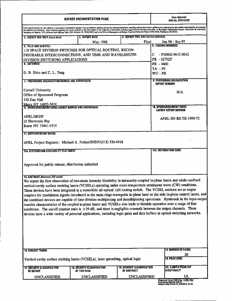
13. ABSTRACT (Maximum 200 words) We report the first observation of two-mode intensity bistability in intracavity-coupled in-plane lasers and oxide-confined vertical-cavity surface emitting lasers (VCSELs) operating under room-temperature continuous wave (CW) conditions. These devices have been integrated in a monolithic all-optical lxN routing switch. The VCSEL sections act as output couplers for modulation signals introduced to the main ridge-waveguide in-plane laser or the side in-plane control lasers, and the combined devices are capable of time-division multiplexing and demultiplexing operations. Hysteresis in the input-output transfer characteristics of the coupled in-plane lasers and VCSELs also leads to bistable operation over a range of bias conditions. The on/off contrast ratio is >29 dB, and there is negligible crosstalk between the output channels. These devices have a wide variety of potential applications, including logic gates and data buffers in optical switching networks.
14. SUBJECT TERMS
Vertical-cavity surface emitting lasers (VCSELs), laser quenching, optical logic
17. SECURITY CLASSIFICATION OF REPORT
UNCLASSIFIED
18. SECURITY CLASSIFICATION OF THIS PAGE
UNCLASSIFIED
IS. SECURITY CLASSIFICATION OF ABSTRACT
UNCLASSIFIED
15. NUMBER OF PAGES
20 16. PRICE CODE
20. LIMITATION OF ABSTRACT
UL Standard Form 298 (Rev. 2-89) (EG) Prescribed by ANSI Std. 238.1« Designed using Perform Pre. WHSIDIOR. Oct 94
Table Of Contents
Acknowledgments 11
Executive Summary iii
I. Bistable Operation of Coupled In-Plane and Oxide-Confined 1
Vertical-Cavity Laser lxN Routing Switches
Fig. 1. (a) A schematic diagram of an all-optical 1x3 routing switch, and
(b) a SEM micrograph of a completed device. 6
Fig. 2. Demonstration of the routing switch operation. 7
Fig. 3. Hysteresis in the routing switch input/output transfer characteristic. 8
II. Conclusions and Future Work 9
References 10
Acknowledgments
The authors wish to acknowledge the valuable technical collaboration with Dr. Michael
Parker of the Rome Laboratory Photonics Center on this research program, and technical
discussions and training from S. Pesarcik and the staff of the Cornell Nanofabrication Facility. C.
Lei and L. Hodge of Hewlett-Packard Company's Components Group supplied some of the
epitaxial material used in the fabrication of the devices discussed here, and J. L. Rossi of Rome
Laboratory was also of valuable assistance with administration of this work.
11
Executive Summary
We report the first observation of two-mode intensity bistability in intracavity-coupled in-
plane lasers and oxide-confined vertical-cavity surface emitting lasers (VCSELs) operating under
room-temperature CW conditions. These devices have been integrated in a monolithic all-optical
lxN routing switch. The VCSEL sections act as output couplers for modulation signals introduced
to the main ridge-waveguide in-plane laser or the side in-plane control lasers, and the combined
devices are capable of time-division multiplexing and demultiplexing operations. Hysteresis in the
input/output transfer characteristics of the coupled in-plane lasers and VCSELs also leads to
bistable operation over a range of bias conditions. The on/off contrast ratio is >20 dB, and there is
negligible crosstalk between the output channels. These devices have a wide variety of potential
applications, including logic gates and data buffers in optical switching networks.
11X
Bistable Operation of Coupled In-Plane and Oxide-Confined
Vertical-Cavity Laser lxN Routing Switches
We report the first experimental demonstration of bistable operation in intracavity-coupled
in-plane lasers and oxide-confined VCSELs. This effect is demonstrated in a monolithically-
integrated all-optical 1 x N routing switch which operates CW at room temperature. It has been
shown both theoretically and experimentally that intracavity-coupled lasers can exhibit complete
gain quenching of the stimulated emission in the controlled device, as well as bistability in their
input-output characteristic1"6. These coupled lasers can be fabricated in any number of
combinations in order to achieve the desired logic, routing, or memory functions. For example,
Shire et al. have demonstrated a NOR gate based on mode competition in a shared laser gain
region2, and Johnson et al. demonstrated an all-optical flip-flop based on the same principle4. This
work is distinct from bistable switching laser designs which have employed saturable absorber
sections in a main laser which are then controlled by injecting side light into the absorber(s). In
this case, the gain region common to the intersecting in-plane lasers is the VCSEL output device
itself, which is independently biased. In addition to serving as a large-aperture output coupler for
the modulation signal from the main in-plane laser, the VCSEL facilitates signal transmission via
free space or optical fibers by virtue of its low-divergence output beam.
The bistability we observe may be used for optical memory purposes or for digital optical
signal regeneration due to the combined laser device's thresholding capability. Furthermore, the
waveform regeneration and reshaping properties and the concomitant improvement in the bit error
rate of degraded optical inputs (such as clock signals) observed by Nonaka et al. are also expected
here7-9. While bistable operation had been anticipated in our earlier work10, we now present clear-
cut evidence of hysteresis over a range of bias conditions which leads to increased functionality of
the routing switches, e.g. in time-slot interchange systems. The processing improvements which
have led to the current generation of room-temperature CW devices have been the application of
oxide confinement techniques to the epitaxial material to achieve low threshold current in the
VCSEL sections, and careful control of the chemically-assisted ion beam etching (CAIBE) process
for etching the in-plane laser end mirrors.
Lately, much attention been focused on all-optical signal routing, wavelength switching and
conversion by means of semiconductor optical amplifiers, due to their fast carrier and gain
dynamics. This has been achieved using cross-gain compression11, four-wave mixing, or Mach-
Zehnder based cross-phase modulation12. Likewise, all-optical switching has also been achieved
through electro-optic or third-order nonlinear effects in optical materials such as LiNbC>3 13 or
optical fiber itself. None of these approaches, though, offer the advantages of complete monolithic
integration on a single chip, together with gain, in a design which is compatible with standard laser
fabrication techniques. We demonstrate here a 1 x 3 routing switch which is capable of time
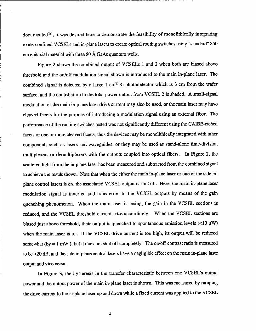
division multiplexing and demultiplexing operations. The device is shown schematically in Figure
1, together with a SEM micrograph of a typical device. The main in-plane ridge-waveguide laser is
10 x 400 ^m long, and its cavity contains three VCSEL output sections, each with an 8 \im2 oxide
aperture. The VCSEL sections have 10 x 200 |im side in-plane control lasers fabricated adjacent to
them, and a passive in-plane laser mirror is etched on the opposite side of each VCSEL. The
passive mirror section is required in order to oxidize the VCSEL mesa from all sides after defining
the lasers by one-step two-level etching14.
The fabrication process was as follows. After protecting the VCSEL apertures and
depositing SiC»2 and Cr etch masks for the ridge waveguides and end the end mirrors respectively,
the CAIBE etching was performed. In this way, the entire combined-laser structure was created in
a single etching operation. The in-plane laser ridges were then protected from oxidation, and the
samples were loaded into a furnace at 400 °C through which 3 slm N2 gas (bubbled through 85 °C
DIH2O) flowed for 12 min. No delamination of the oxidized AlAs-based DBR structures was
observed, as was noted previously by Choquette et al.15. Special care was taken, though, to not
expose the samples to rapid temperature fluctuations (e.g., later rapid thermal alloying of the
contacts) after oxidation. While the desirable effects of a single oxide aperture above and/or below
the active region of a VCSEL for reducing its threshold current have been thoroughly
documented16, it was desired here to demonstrate the feasibility of monolithically integrating
oxide-confined VCSELs and in-plane lasers to create optical routing switches using "standard" 850
nm epitaxial material with three 80 Ä GaAs quantum wells.
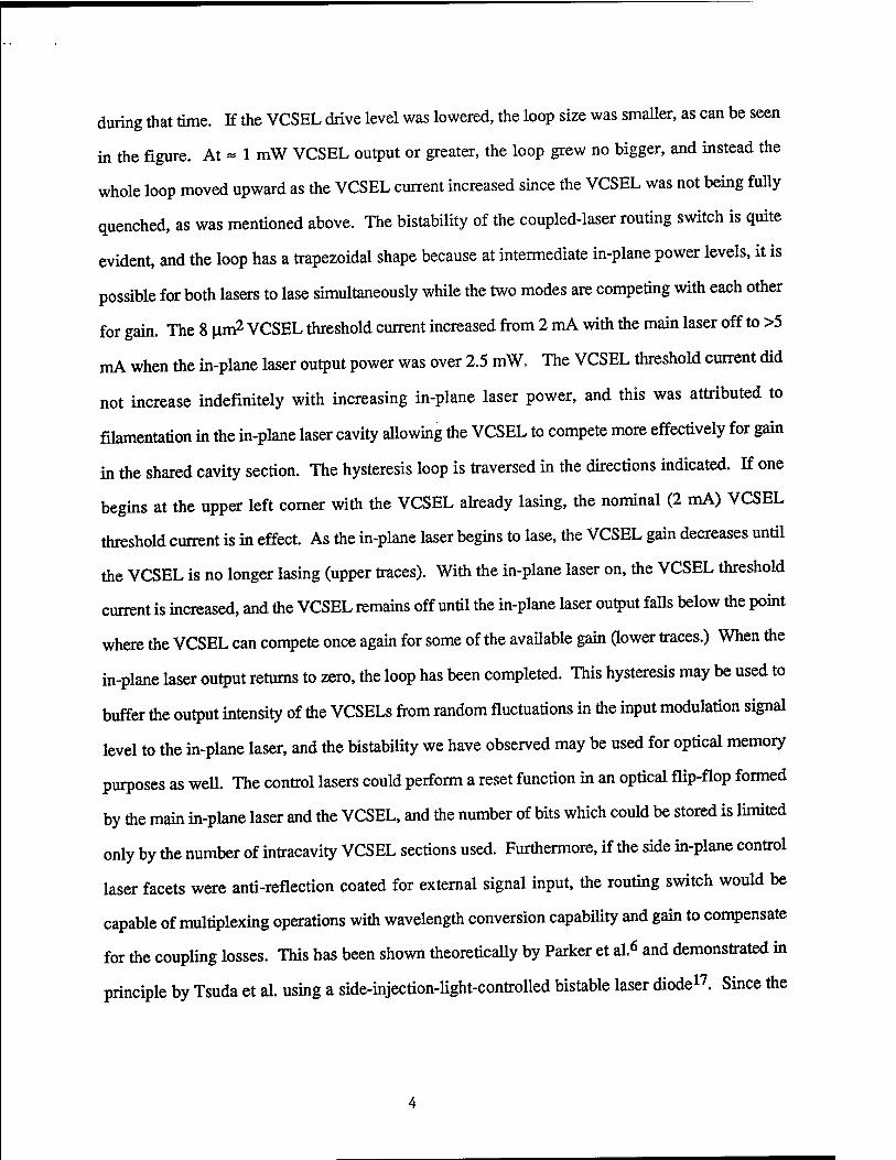
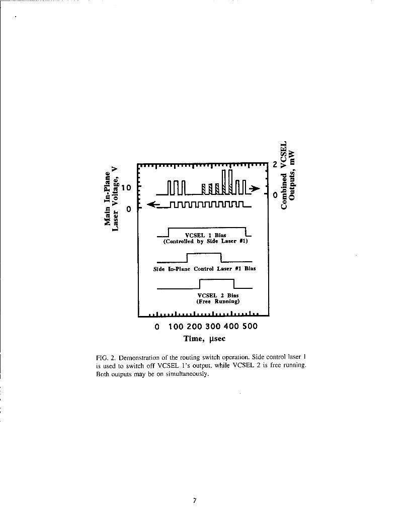
Figure 2 shows the combined output of VCSELs 1 and 2 when both are biased above
threshold and the on/off modulation signal shown is introduced to the main in-plane laser. The
combined signal is detected by a large 1 cm2 Si photodetector which is 3 cm from the wafer
surface, and the contribution to the total power output from VCSEL 2 is shaded. A small-signal
modulation of the main in-plane laser drive current may also be used, or the main laser may have
cleaved facets for the purpose of introducing a modulation signal using an external fiber. The
performance of the routing switches tested was not significantly different using the CAIBE-etched
facets or one or more cleaved facets; thus the devices may be monolithically integrated with other
components such as lasers and waveguides, or they may be used as stand-alone time-division
multiplexers or demultiplexers with the outputs coupled into optical fibers. In Figure 2, the
scattered light from the in-plane laser has been measured and subtracted from the combined signal
to achieve the result shown. Note that when the either the main in-plane laser or one of the side in-
plane control lasers is on, the associated VCSEL output is shut off. Here, the main in-plane laser
modulation signal is inverted and transferred to the VCSEL outputs by means of the gain
quenching phenomenon. When the main laser is lasing, the gain in the VCSEL sections is
reduced, and the VCSEL threshold currents rise accordingly. When the VCSEL sections are
biased just above threshold, their output is quenched to spontaneous emission levels (<10 ^W)
when the main laser is on. If the VCSEL drive current is too high, its output will be reduced
somewhat (by ~ 1 mW), but it does not shut off completely. The on/off contrast ratio is measured
to be >20 dB, and the side in-plane control lasers have a negligible effect on the main in-plane laser
output and vice versa.
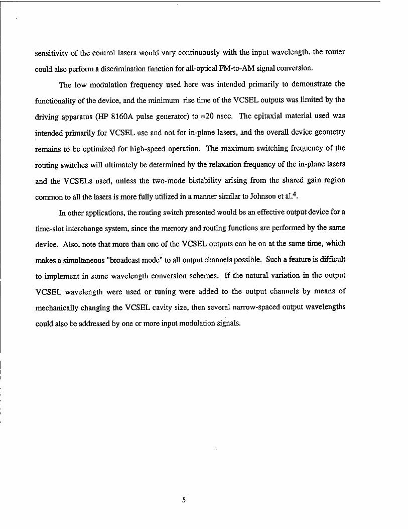
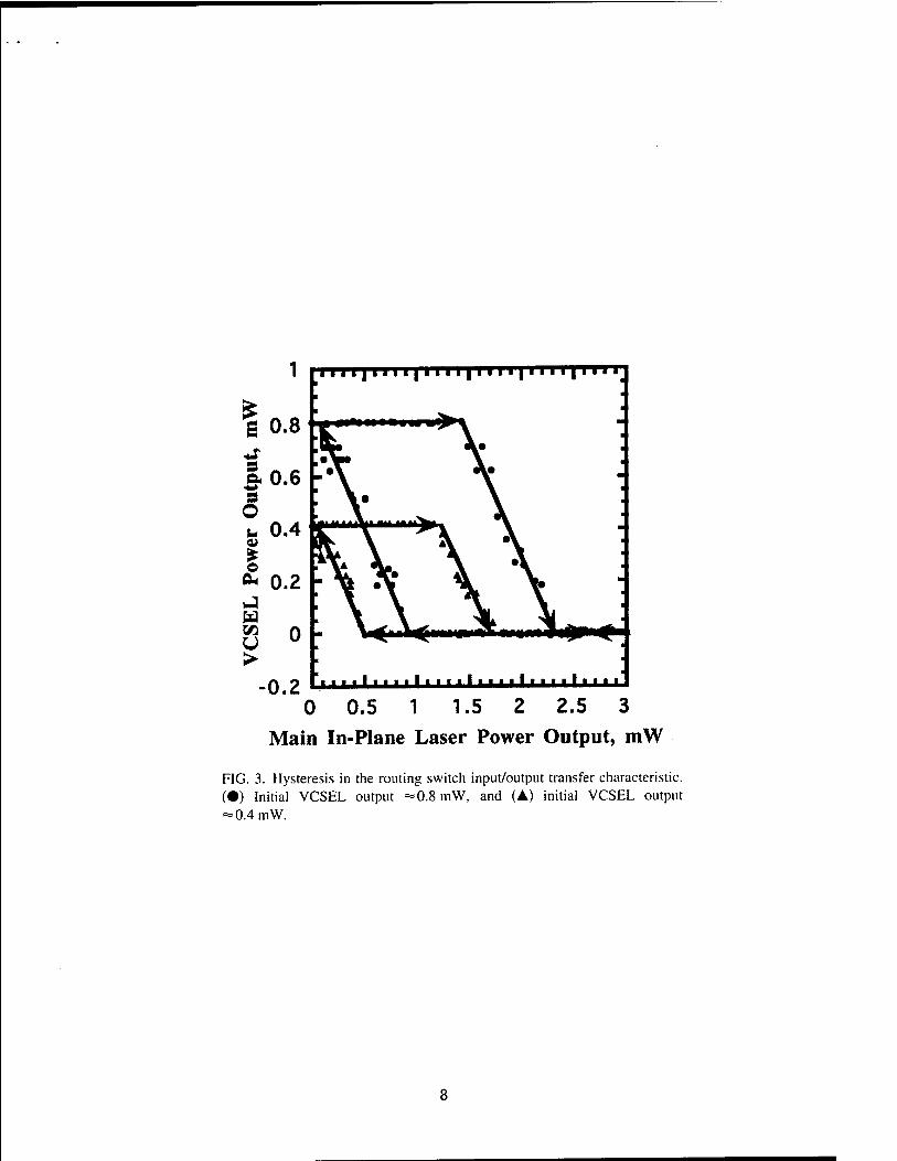
In Figure 3, the hysteresis in the transfer characteristic between one VCSEL's output
power and the output power of the main in-plane laser is shown. This was measured by ramping
the drive current to the in-plane laser up and down while a fixed current was applied to the VCSEL
during that time. If the VCSEL drive level was lowered, the loop size was smaller, as can be seen
in the figure. At « 1 mW VCSEL output or greater, the loop grew no bigger, and instead the
whole loop moved upward as the VCSEL current increased since the VCSEL was not being fully
quenched, as was mentioned above. The bistability of the coupled-laser routing switch is quite
evident, and the loop has a trapezoidal shape because at intermediate in-plane power levels, it is
possible for both lasers to läse simultaneously while the two modes are competing with each other
for gain. The 8 ^m2 VCSEL threshold current increased from 2 mA with the main laser off to >5
mA when the in-plane laser output power was over 2.5 mW. The VCSEL threshold current did
not increase indefinitely with increasing in-plane laser power, and this was attributed to
fflamentation in the in-plane laser cavity allowing the VCSEL to compete more effectively for gain
in the shared cavity section. The hysteresis loop is traversed in the directions indicated. If one
begins at the upper left corner with the VCSEL already lasing, the nominal (2 mA) VCSEL
threshold current is in effect. As the in-plane laser begins to läse, the VCSEL gain decreases until
the VCSEL is no longer lasing (upper traces). With the in-plane laser on, the VCSEL threshold
current is increased, and the VCSEL remains off until the in-plane laser output falls below the point
where the VCSEL can compete once again for some of the available gain (lower traces.) When the
in-plane laser output returns to zero, the loop has been completed. This hysteresis may be used to
buffer the output intensity of the VCSELs from random fluctuations in the input modulation signal
level to the in-plane laser, and the bistability we have observed may be used for optical memory
purposes as well. The control lasers could perform a reset function in an optical flip-flop formed
by the main in-plane laser and the VCSEL, and the number of bits which could be stored is limited
only by the number of intracavity VCSEL sections used. Furthermore, if the side in-plane control
laser facets were anti-reflection coated for external signal input, the routing switch would be
capable of multiplexing operations with wavelength conversion capability and gain to compensate
for the coupling losses. This has been shown theoretically by Parker et al.6 and demonstrated in
principle by Tsuda et al. using a side-injection-light-controlled bistable laser diode17. Since the
sensitivity of the control lasers would vary continuously with the input wavelength, the router
could also perform a discrimination function for all-optical FM-to-AM signal conversion.
The low modulation frequency used here was intended primarily to demonstrate the
functionality of the device, and the minimum rise time of the VCSEL outputs was limited by the
driving apparatus (HP 8160A pulse generator) to «20 nsec. The epitaxial material used was
intended primarily for VCSEL use and not for in-plane lasers, and the overall device geometry
remains to be optimized for high-speed operation. The maximum switching frequency of the
routing switches will ultimately be determined by the relaxation frequency of the in-plane lasers
and the VCSELs used, unless the two-mode bistability arising from the shared gain region
common to all the lasers is more fully utilized in a manner similar to Johnson et alA
In other applications, the routing switch presented would be an effective output device for a
time-slot interchange system, since the memory and routing functions are performed by the same
device. Also, note that more than one of the VCSEL outputs can be on at the same time, which
makes a simultaneous "broadcast mode" to all output channels possible. Such a feature is difficult
to implement in some wavelength conversion schemes. If the natural variation in the output
VCSEL wavelength were used or tuning were added to the output channels by means of
mechanically changing the VCSEL cavity size, then several narrow-spaced output wavelengths
could also be addressed by one or more input modulation signals.
f Passive, Deep-Etched In-Plane Laser Mirror
f Oxide-Confined VCSEL Section
j! 10 ^m Shallow-Etched " Coupling Gap
Deep-Etched In-Plane
Mirror at End of Ridge Waveguide
(b) 100 um
FIG. 1. (a) A schematic diagram of an all-optical 1 X 3 routing switch, and (b) a SEM micrograph of a completed device.
> 0)
Co ; JUULJlUL*: 1 ^z_jrnnrinrinnnnrL-
I VCSEL 1 Bias L (Controlled by Side Laser #1)
Side In-Plane Control Laser #1 Bias
VCSEL 2 Bias (Free Running)
..I •'■■'■■■■' JU I.
0 100 200 300 400 500
Time, usec
v S
■2 s
1°
FIG. 2. Demonstration of the routing switch operation. Side control laser 1 is used to switch off VCSEL l's output, while VCSEL 2 is free running. Both outputs may be on simultaneously.
11111111111111111111111111111
■ ■■■■■ . I.... i.... I.... I 0.2 0 0.5 1 1.5 2 2.5 3
Main In-Plane Laser Power Output, mW
FIG. 3. Hysteresis in the routing switch input/output transfer characteristic. (•) Initial VCSEL output =0.8 mW, and (A) initial VCSEL output = 0.4 mW.

Conclusions and Future Work
In conclusion, we have demonstrated bistable operation in intracavity-coupled in-plane
lasers and oxide-confined VCSELs. These were implemented in a monolithically-integrated all-
optical 1x3 routing switch which operated CW at room temperature. The on/off contrast ratio
was >20 dB, and there was negligible crosstalk between the output devices. The routing switches
have a thresholding feature due to the hysteresis in the output power vs. input power transfer
characteristic, and they have time division multiplexing and demultiplexing capabilities as well.
The goals of the original Expert in Science and Engineering grant and its extension have been
largely met; that is, the oxidation furnace for AlGaAs materials was constructed, VCSELs and in-
plane lasers were made in part by using this system, and the resulting routing switches that were
fabricated made room-temperature characterization of these devices possible. A clear-cut
demonstration was made of the two-mode bistability which had long been predicted in intracavity-
coupled lasers with overlapping gain regions, and the opening of the hysteresis loop in input
power-output power space has been measured. The foundation has thus been laid for future work
in which subsystems employing the all-optical switching devices developed here are demonstrated,
including time-slot interchange circuits and transmitters for dense wavelength-division multiplexed
transmission systems.

References
[I] D. B. Shire, M. A. Parker, P. D. Swanson, J. S. Kimmet, and C. L. Tang, Appl. Phys. Lett. 66, 1717 (1995).
[2] D. B. Shire, M. A. Parker, and C. L. Tang, IEEE Photon. Technol. Lett. 8,188 (1996).
[3] C. L. Tang, A. Schremer, and T. Fujita, Appl. Phys. Lett. 51 1392 (1987).
[4] J. E. Johnson, C. L. Tang, and W. J. Grande, Appl. Phys. Lett. 63 3273 (1993).
[5] M. A. Parker and D. B. Shire, Appl. Phys. Lett 70 146 (1997).
[6] M. A. Parker and D. B. Shire, J. Appl. Phys., submitted for publication (1997).
[7] K. Nonaka and T. Kurokawa, Electron. Lett. 311865 (1995).
[8] K. Nonaka, Y. Noguchi, H. Tsuda, and T. Kurokawa, in Proc. 14th IEEE International Semiconductor Laser Conference 229(1994).
[9] K. Nonaka and T. Kurokawa, in Proc. International Topical Meeting on Optical Computing - OC '96 48 (1996).
[10] D. B. Shire, C. L. Tang, M. Hong, and J. D. Wynn, IEEE Photon. Technol. Lett. 8, 1537 (1996).
[II] J. M. Wiesenfeld, J. S. Perino, A. S. Gnauck, and B. Glance, Electron. Lett 30,720 (1994).
[12] B. Mikkelson, T. Durhuus, C. Joergenson, R. J. S. Pedersen, C. Braagaard, and K. E. Stubkjaer, Electron. Lett. 30, 260 (1994).
[13] R. C. Alferness, N. P. Economou, and L. L. Buhl, Appl. Phys. Lett. 38, 214 (1981).
[14] W. J. Grande, J. E. Johnson, and C. L. Tang, Appl. Phys. Lett. 57 2537 (1990).
[15] K. D. Choquette, K. M. Geib, H. C. Chui, B. E. Hammons, H. Q. Hou, T. J. Drummond, and R. Hull, Appl. Phys. Lett 69 1385 (1996).
[16] K. D. Choquette, W. W. Chow, M. Hagerott Crawford, K. M. Geib, and R. P. Schneider, Jr., Appl. Phys. Lett. 68 3689 (1996).
[17] H. Tsuda, K. Nonaka, K. Hirabayashi, H. Uenohara, H. Iwamura, and T. Kurokawa, Appl. Phys. Lett. 63 3116 (1993).
10