tailor-made nanomaterials designed by electrochemical methods
TRANSCRIPT
Electrochimica Acta 49 (2003) 51–61
Tailor-made nanomaterials designed by electrochemical methods
Harald Natter∗, Rolf Hempelmann
Universität des Saarlandes, Physikalische Chemie, D-66123 Saarbrücken, Germany
Received 3 December 2002; accepted 15 April 2003
Abstract
We have developed different electrochemical procedures for the production of nanostructured bulk metals, catalyst particles and metaloxides with variable crystallite sizes. The crystallite size of the nanoparticles can be controlled by the variation of the physical and chemicalprocess parameters. Efficient and inexpensive catalyst layers for polymer electrolyte fuel cells were prepared using pulsed electrodeposition(PED) and DC-plating procedures. The advantage of these techniques is the site-selective deposition of Pt and PtRu catalysts on the carbonsupport. Large amounts of nanostructured metal oxides with different crystallite sizes can be prepared with our EDOC process (electrochemicaldeposition under oxidizing conditions) which is based on the reduction of metal ions generated from the anodic dissolution of a sacrificialanode with subsequent oxidation of the formed metal clusters. For these nanomaterials we also discuss the physical properties (e.g. thermalstability, catalytic activity).© 2003 Elsevier Ltd. All rights reserved.
Keywords: Nanostructured metals; Fuel cell catalysts; Nanostructured oxides; Pulsed electrodeposition
1. Introduction
The preparation of nanostructured materials by electro-chemical procedures has found worldwide much attention[1–3], because these techniques allow the variation of thecrystallite size, and therefore the physical and chemicalproperties can be controlled. The defined variation of thecrystallite size is necessary because many chemical andphysical properties of nanostructured materials depend on it[4]. Only by the variation of the crystallite size it is possibleto improve certain physical property of one and the samematerial, e.g. the enhanced hardness of nano-Au, the tough-ness of nano-Ni/P alloys[5], the soft magnetic properties ofnano-Ni [6] and the corrosion resistance of nanostructuredalloys [7] promise industrial applications[8,9].
The production of such “tailor-made” nanomaterials byelectrochemical procedures is very advantageous becausethe crucial steps in nanocrystal formation, the nuclei forma-tion and nuclei growth, can be controlled by the physical-(e.g. current density, current characteristics) and chemicalparameters (grain refiners, complex formers)[10,11].
∗ Corresponding author. Tel.:+681-302-3029; fax:+681-302-4759.E-mail address: [email protected] (H. Natter).
In the following contribution we present three examplesfor the “tailor-made” production of nanostructured materialsby electrochemical procedures:
1. Preparation of nanostructured metals and alloys by pulsedelectrodeposition (PED);
2. Deposition of nano oxide powders using the EDOC pro-cess;
3. In situ preparation of platinum and PtRu catalysts in fuelcell membranes.
2. Preparation of nanostructured metals and alloys bypulsed electrodeposition
The pulsed electrodeposition technique is a versatilemethod for the preparation of nanostructured metals andalloys [12]. In the last two decades the PED has foundworldwide much attention, because this technique allowsthe preparation of large bulk samples with high purity, lowporosity and enhanced thermal stability. InSection 2.4wediscuss the pulse reverse technique for stabilizing nanos-tructured nickel by segregation of nickel oxide into thegrain boundaries. In this way nanostructures with crystallitesizes of 40 nm can be stabilized at temperatures of 700 K.
0013-4686/$ – see front matter © 2003 Elsevier Ltd. All rights reserved.doi:10.1016/j.electacta.2003.04.004
52 H. Natter, R. Hempelmann / Electrochimica Acta 49 (2003) 51–61
Furthermore, this electrochemical procedure enables to in-tentionally adjust the nanostructure (grain-size, grain-sizedistribution, microstress) which are responsible for thephysical and chemical properties.
2.1. Fundamental aspects of PED
The electrochemical deposition of nanostructured materi-als is a two-step process:
1. The formation of a high nuclei number;2. The controlled growth of the deposited nuclei.
These two conditions can be realized by the proper choiceof the chemical and physical process parameters. The sizeand the number of nuclei can be controlled by the overvolt-age (η):
r = 2σV
ze0|η| (1)
In this electrochemical version of the Kelvin equation[13]r means the critical nucleation radius,σ the specific surfaceenergy,V the atomic volume in the crystal,z the number ofelementary chargese0. Eq. (1) reveals the higher the over-voltage the smaller the formed nuclei, that means by apply-ing a high overvoltage we get a high current density whichis responsible for a high nuclei formation rate. This high de-position rate can be maintained for only a few milliseconds(ton-time) because the metal ion concentration in the vicinityof the cathode decreases drastically and therefore the pro-cess becomes diffusion-controlled. For this reason the cur-rent pulse is switched off for 20–100 ms (toff -time). Duringthe toff -time the metal ions diffuse from the bulk electrolyteto the cathode and compensate the metal ion depletion. Inthis break we observe a second effect: due to exchange cur-rents Ostwald ripening sets in and causes crystallite growth.Based on these facts we have several possibilities to controlthe crystallite size (experimental data for n-gold depositionwill be presented inSection 2.2):
1. The current density is responsible for the nuclei size and– number. In the case of a constant charge per cycle thecrystallite size can be decreased by increasing the currentdensity.
2. For a constantton-time and current density, the crystallitesize increases for longtoff -times due to Ostwald ripening;
3. The use of organic additives (grain refiners) enables thecontrol of the crystallization process during thetoff -timebecause these molecules are adsorbed on the electrodesurface in a reversible way and hinder the surface diffu-sion of the adatoms;
4. The temperature influences all diffusion processes (iondiffusion in the electrolyte, surface diffusion of the nu-clei). If small crystallite sizes are desired the depositionshould be performed at ambient temperatures or belowbecause the recrystallisation of the nuclei is strongly re-
duced by a decreased velocity of the adatoms and themetal ions.
The bath composition, the pH-value, the hydrodynamicconditions and also the use of special current shapes arefurther possibilities to control the crystallite size.
2.2. Variation of the crystallite size: experimental details
All experiments are performed in a double-walled platingcell with a volume of 400 ml. The temperature is kept on aconstant value using a thermostatic unit. We choose for ourexperiments the galvanostatic mode because the average de-position rate can be simply derived fromEq. (2)whereas involtage regulation mode the average deposition rate can bepredicted only from computations. The main advantage ofthe pulsed voltage method is the better control of the currentefficiency and the alloy composition. From the experimen-tal point of view the potentiostatic mode is very difficult torealize because a three-electrode setup is necessary. To getinstantaneously a desired potential at the electrode the cur-rent should start theoretically from an infinite value, whichis not feasible because of the limitation of the electronicequipment. In the potentiostatic mode we need a short re-verse pulse to fix the initial potential, which is not generallydesirable because passivation may occur during this reversepotential pulse. For these reasons it is easier to regulate thecurrent.
The output current pulse of the galvanostatic unit (KepcoElectronic Inc., IL, USA) was generated with a pulse gener-ator (Hameg Elektronik, Germany) which enables off-timesbetween 1 and 500 ms and on times between 1 and 100 ms.The maximum current density is 5 A/cm2.
Transmission electron microscopy (TEM) and X-raydiffraction (XRD) were used for crystallite size determina-tion. We get the crystallite size, the crystallite size distribu-tion and the content of micro strain from a X-ray patternevaluated with the Warren/Averbach technique[21–23]. Alldetails of our modified procedure are described elsewhere[10,14,24].
All samples were deposited onto stainless steel or titaniumelectrodes (20 mm×20 mm). The distance between the elec-trodes is 25 mm. The n-gold samples were deposited from aconventional gold(I)sulfite bath (AS-15) received from Her-aeus Kulzer GmbH (Hanau, Germany). This type of elec-trolyte can be prepared by dissolving gold(I)chloride in am-monium sulfite solution[25]. For a better comparability ofthe individual results we perform the experiments at an av-erage current density (Iav) of 3 mA/cm2:
Iav = Ipulseton
ton + toff(2)
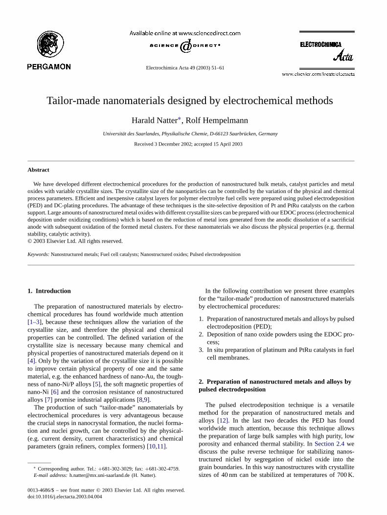
In a first series of experiments we optimize the pulse cur-rent density (Ipulse). ton and toff is kept at a constant value(details seeFig. 1). We find the smallest crystallite size of12 nm at aIpulse value of 0.5 A/cm2 (seeFig. 1). For higher
H. Natter, R. Hempelmann / Electrochimica Acta 49 (2003) 51–61 53
10
15
20
25
30
35
40
45
0 100 200 300 400 500
n-gold depositionton
: 2 mstoff
: 78 msT: 35˚C
current density / mA/cm2
crys
talli
te s
ize
/ n
m
Fig. 1. The crystallite size dependence of the pulsed current densityfor gold deposits deposited from a commercial sulfite bath without anyadditives.
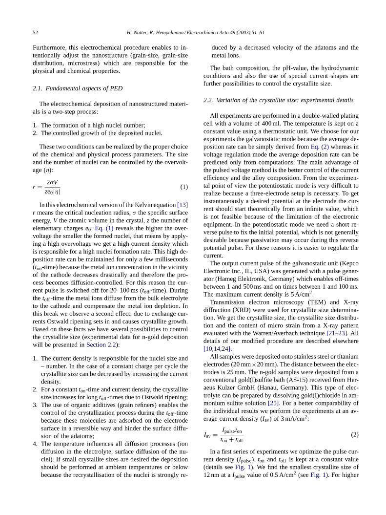
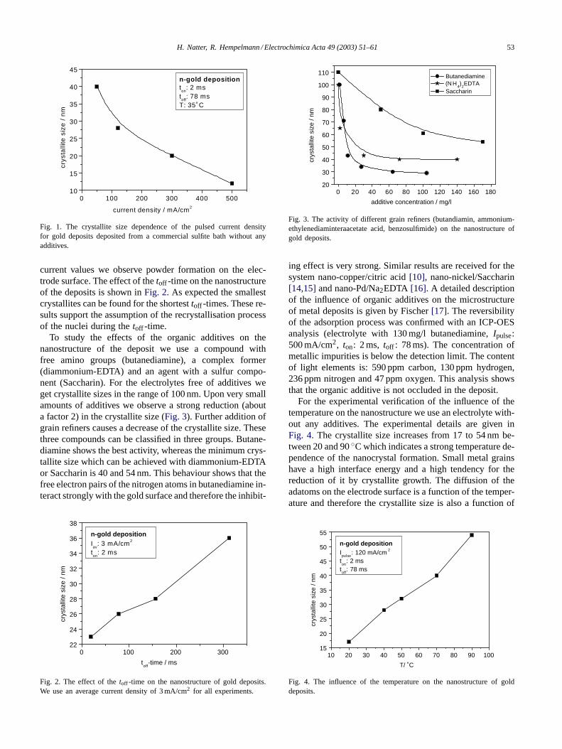
current values we observe powder formation on the elec-trode surface. The effect of thetoff -time on the nanostructureof the deposits is shown inFig. 2. As expected the smallestcrystallites can be found for the shortesttoff -times. These re-sults support the assumption of the recrystallisation processof the nuclei during thetoff -time.
To study the effects of the organic additives on thenanostructure of the deposit we use a compound withfree amino groups (butanediamine), a complex former(diammonium-EDTA) and an agent with a sulfur compo-nent (Saccharin). For the electrolytes free of additives weget crystallite sizes in the range of 100 nm. Upon very smallamounts of additives we observe a strong reduction (abouta factor 2) in the crystallite size (Fig. 3). Further addition ofgrain refiners causes a decrease of the crystallite size. Thesethree compounds can be classified in three groups. Butane-diamine shows the best activity, whereas the minimum crys-tallite size which can be achieved with diammonium-EDTAor Saccharin is 40 and 54 nm. This behaviour shows that thefree electron pairs of the nitrogen atoms in butanediamine in-teract strongly with the gold surface and therefore the inhibit-
22
24
26
28
30
32
34
36
38
0 100 200 300
n-gold depositionIav
: 3 mA/cm2
ton
: 2 ms
toff
-time / ms
crys
talli
te s
ize
/ nm
Fig. 2. The effect of thetoff -time on the nanostructure of gold deposits.We use an average current density of 3 mA/cm2 for all experiments.
20
30
40
50
60
70
80
90
100
110
0 20 40 60 80 100 120 140 160 180
Butanediamine (N H
4)
2EDTA
Saccharin
additive concentration / mg/l
crys
talli
te s
ize
/ nm
Fig. 3. The activity of different grain refiners (butandiamin, ammonium-ethylenediaminteraacetate acid, benzosulfimide) on the nanostructure ofgold deposits.
ing effect is very strong. Similar results are received for thesystem nano-copper/citric acid[10], nano-nickel/Saccharin[14,15]and nano-Pd/Na2EDTA [16]. A detailed descriptionof the influence of organic additives on the microstructureof metal deposits is given by Fischer[17]. The reversibilityof the adsorption process was confirmed with an ICP-OESanalysis (electrolyte with 130 mg/l butanediamine,Ipulse:500 mA/cm2, ton: 2 ms, toff : 78 ms). The concentration ofmetallic impurities is below the detection limit. The contentof light elements is: 590 ppm carbon, 130 ppm hydrogen,236 ppm nitrogen and 47 ppm oxygen. This analysis showsthat the organic additive is not occluded in the deposit.
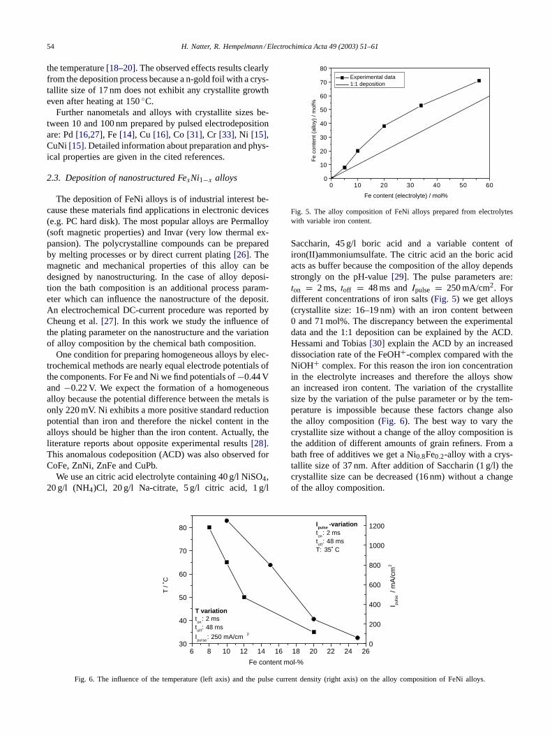
For the experimental verification of the influence of thetemperature on the nanostructure we use an electrolyte with-out any additives. The experimental details are given inFig. 4. The crystallite size increases from 17 to 54 nm be-tween 20 and 90◦C which indicates a strong temperature de-pendence of the nanocrystal formation. Small metal grainshave a high interface energy and a high tendency for thereduction of it by crystallite growth. The diffusion of theadatoms on the electrode surface is a function of the temper-ature and therefore the crystallite size is also a function of
15
20
25
30
35
40
45
50
55
10 20 30 40 50 60 70 80 90 100
n-gold depositionIpulse
: 120 mA/cm 2
ton
: 2 mstoff
: 78 ms
T/ ˚C
crys
talli
te s
ize
/ nm
Fig. 4. The influence of the temperature on the nanostructure of golddeposits.
54 H. Natter, R. Hempelmann / Electrochimica Acta 49 (2003) 51–61
the temperature[18–20]. The observed effects results clearlyfrom the deposition process because a n-gold foil with a crys-tallite size of 17 nm does not exhibit any crystallite growtheven after heating at 150◦C.
Further nanometals and alloys with crystallite sizes be-tween 10 and 100 nm prepared by pulsed electrodepositionare: Pd[16,27], Fe[14], Cu [16], Co [31], Cr [33], Ni [15],CuNi [15]. Detailed information about preparation and phys-ical properties are given in the cited references.
2.3. Deposition of nanostructured FexNi1−x alloys
The deposition of FeNi alloys is of industrial interest be-cause these materials find applications in electronic devices(e.g. PC hard disk). The most popular alloys are Permalloy(soft magnetic properties) and Invar (very low thermal ex-pansion). The polycrystalline compounds can be preparedby melting processes or by direct current plating[26]. Themagnetic and mechanical properties of this alloy can bedesigned by nanostructuring. In the case of alloy deposi-tion the bath composition is an additional process param-eter which can influence the nanostructure of the deposit.An electrochemical DC-current procedure was reported byCheung et al.[27]. In this work we study the influence ofthe plating parameter on the nanostructure and the variationof alloy composition by the chemical bath composition.
One condition for preparing homogeneous alloys by elec-trochemical methods are nearly equal electrode potentials ofthe components. For Fe and Ni we find potentials of−0.44 Vand −0.22 V. We expect the formation of a homogeneousalloy because the potential difference between the metals isonly 220 mV. Ni exhibits a more positive standard reductionpotential than iron and therefore the nickel content in thealloys should be higher than the iron content. Actually, theliterature reports about opposite experimental results[28].This anomalous codeposition (ACD) was also observed forCoFe, ZnNi, ZnFe and CuPb.
We use an citric acid electrolyte containing 40 g/l NiSO4,20 g/l (NH4)Cl, 20 g/l Na-citrate, 5 g/l citric acid, 1 g/l
6 8 10 12 14 16 18 20 22 24 2630
40
50
60
70
80
0
200
400
600
800
1000
1200
T variationton
: 2 mstof f
: 48 ms
Ipul se
: 250 mA/cm 2
Ipulse
-variationton
: 2 mstof f
: 48 msT: 35˚ C
T /
˚C
Fe content mol-%
Ipu
lse /
mA
/cm
2
Fig. 6. The influence of the temperature (left axis) and the pulse current density (right axis) on the alloy composition of FeNi alloys.
0 10 20 30 40 50 600
10
20
30
40
50
60
70
80 Experimental data 1:1 deposition
Fe
cont
ent (
allo
y) /
mol
%
Fe content (electrolyte) / mol%
Fig. 5. The alloy composition of FeNi alloys prepared from electrolyteswith variable iron content.
Saccharin, 45 g/l boric acid and a variable content ofiron(II)ammoniumsulfate. The citric acid an the boric acidacts as buffer because the composition of the alloy dependsstrongly on the pH-value[29]. The pulse parameters are:ton = 2 ms, toff = 48 ms andIpulse = 250 mA/cm2. Fordifferent concentrations of iron salts (Fig. 5) we get alloys(crystallite size: 16–19 nm) with an iron content between0 and 71 mol%. The discrepancy between the experimentaldata and the 1:1 deposition can be explained by the ACD.Hessami and Tobias[30] explain the ACD by an increaseddissociation rate of the FeOH+-complex compared with theNiOH+ complex. For this reason the iron ion concentrationin the electrolyte increases and therefore the alloys showan increased iron content. The variation of the crystallitesize by the variation of the pulse parameter or by the tem-perature is impossible because these factors change alsothe alloy composition (Fig. 6). The best way to vary thecrystallite size without a change of the alloy composition isthe addition of different amounts of grain refiners. From abath free of additives we get a Ni0.8Fe0.2-alloy with a crys-tallite size of 37 nm. After addition of Saccharin (1 g/l) thecrystallite size can be decreased (16 nm) without a changeof the alloy composition.
H. Natter, R. Hempelmann / Electrochimica Acta 49 (2003) 51–61 55
2.4. Thermal stabilization of n-nickel by pulsereverse plating
The grain boundary fraction of nanostructures with acrystallite size of 10 nm is about 10–20% and thereforethe nanosystems tend to reduce their energy by crystallitegrowth. The thermal stability of nanocrystalline materialsis one of their most important properties which is of inter-est for basic research as well as for industrial applicationsat high temperatures because grain growth influences thesize dependent properties, e.g. hardness[34], coercitivity[35,36] or diffusion processes[32,37].
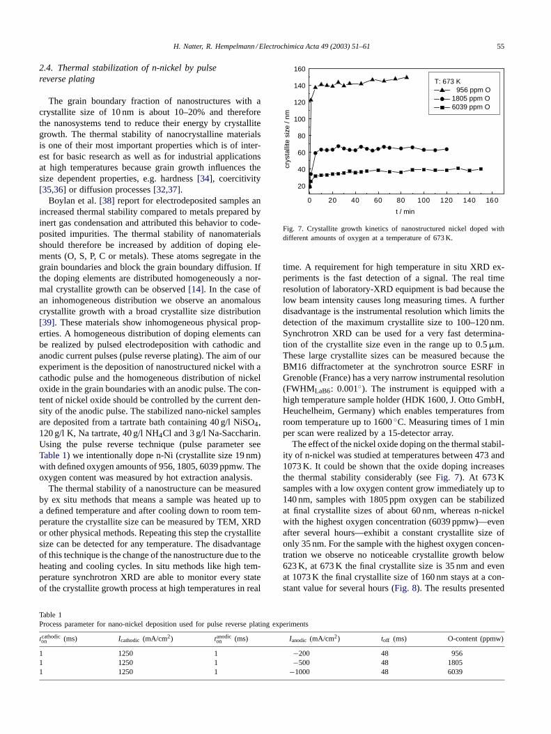
Boylan et al.[38] report for electrodeposited samples anincreased thermal stability compared to metals prepared byinert gas condensation and attributed this behavior to code-posited impurities. The thermal stability of nanomaterialsshould therefore be increased by addition of doping ele-ments (O, S, P, C or metals). These atoms segregate in thegrain boundaries and block the grain boundary diffusion. Ifthe doping elements are distributed homogeneously a nor-mal crystallite growth can be observed[14]. In the case ofan inhomogeneous distribution we observe an anomalouscrystallite growth with a broad crystallite size distribution[39]. These materials show inhomogeneous physical prop-erties. A homogeneous distribution of doping elements canbe realized by pulsed electrodeposition with cathodic andanodic current pulses (pulse reverse plating). The aim of ourexperiment is the deposition of nanostructured nickel with acathodic pulse and the homogeneous distribution of nickeloxide in the grain boundaries with an anodic pulse. The con-tent of nickel oxide should be controlled by the current den-sity of the anodic pulse. The stabilized nano-nickel samplesare deposited from a tartrate bath containing 40 g/l NiSO4,120 g/l K, Na tartrate, 40 g/l NH4Cl and 3 g/l Na-Saccharin.Using the pulse reverse technique (pulse parameter seeTable 1) we intentionally dope n-Ni (crystallite size 19 nm)with defined oxygen amounts of 956, 1805, 6039 ppmw. Theoxygen content was measured by hot extraction analysis.
The thermal stability of a nanostructure can be measuredby ex situ methods that means a sample was heated up toa defined temperature and after cooling down to room tem-perature the crystallite size can be measured by TEM, XRDor other physical methods. Repeating this step the crystallitesize can be detected for any temperature. The disadvantageof this technique is the change of the nanostructure due to theheating and cooling cycles. In situ methods like high tem-perature synchrotron XRD are able to monitor every stateof the crystallite growth process at high temperatures in real
Table 1Process parameter for nano-nickel deposition used for pulse reverse plating experiments
tcathodicon (ms) Icathodic (mA/cm2) tanodic
on (ms) Ianodic (mA/cm2) toff (ms) O-content (ppmw)
1 1250 1 −200 48 9561 1250 1 −500 48 18051 1250 1 −1000 48 6039
0 20 40 60 80 100 120 140 160
20
40
60
80
100
120
140
160
T: 673 K 956 ppm O 1805 ppm O 6039 ppm O
crys
talli
te s
ize
/ nm
t / min
Fig. 7. Crystallite growth kinetics of nanostructured nickel doped withdifferent amounts of oxygen at a temperature of 673 K.
time. A requirement for high temperature in situ XRD ex-periments is the fast detection of a signal. The real timeresolution of laboratory-XRD equipment is bad because thelow beam intensity causes long measuring times. A furtherdisadvantage is the instrumental resolution which limits thedetection of the maximum crystallite size to 100–120 nm.Synchrotron XRD can be used for a very fast determina-tion of the crystallite size even in the range up to 0.5�m.These large crystallite sizes can be measured because theBM16 diffractometer at the synchrotron source ESRF inGrenoble (France) has a very narrow instrumental resolution(FWHMLaB6: 0.001◦). The instrument is equipped with ahigh temperature sample holder (HDK 1600, J. Otto GmbH,Heuchelheim, Germany) which enables temperatures fromroom temperature up to 1600◦C. Measuring times of 1 minper scan were realized by a 15-detector array.
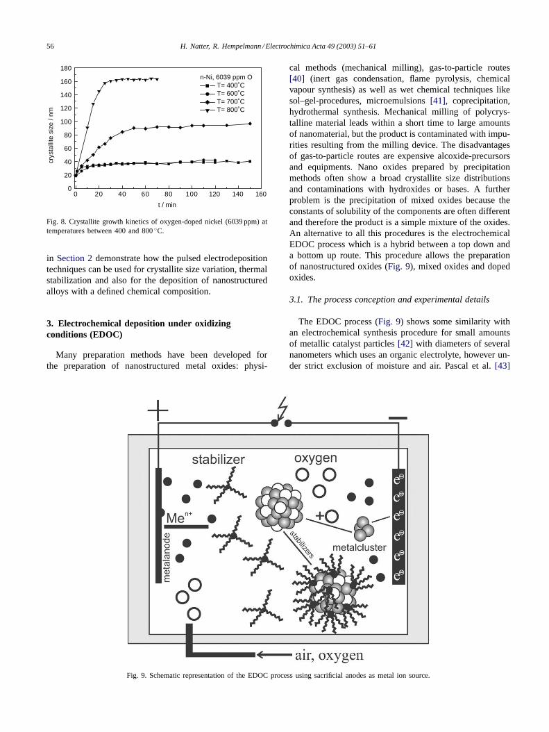
The effect of the nickel oxide doping on the thermal stabil-ity of n-nickel was studied at temperatures between 473 and1073 K. It could be shown that the oxide doping increasesthe thermal stability considerably (seeFig. 7). At 673 Ksamples with a low oxygen content grow immediately up to140 nm, samples with 1805 ppm oxygen can be stabilizedat final crystallite sizes of about 60 nm, whereas n-nickelwith the highest oxygen concentration (6039 ppmw)—evenafter several hours—exhibit a constant crystallite size ofonly 35 nm. For the sample with the highest oxygen concen-tration we observe no noticeable crystallite growth below623 K, at 673 K the final crystallite size is 35 nm and evenat 1073 K the final crystallite size of 160 nm stays at a con-stant value for several hours (Fig. 8). The results presented
56 H. Natter, R. Hempelmann / Electrochimica Acta 49 (2003) 51–61
0 20 40 60 80 100 120 140 1600
20
40
60
80
100
120
140
160
180n-Ni, 6039 ppm O
T= 400˚CT= 600˚CT= 700˚CT= 800˚C
crys
talli
te s
ize
/ nm
t / min
Fig. 8. Crystallite growth kinetics of oxygen-doped nickel (6039 ppm) attemperatures between 400 and 800◦C.
in Section 2demonstrate how the pulsed electrodepositiontechniques can be used for crystallite size variation, thermalstabilization and also for the deposition of nanostructuredalloys with a defined chemical composition.
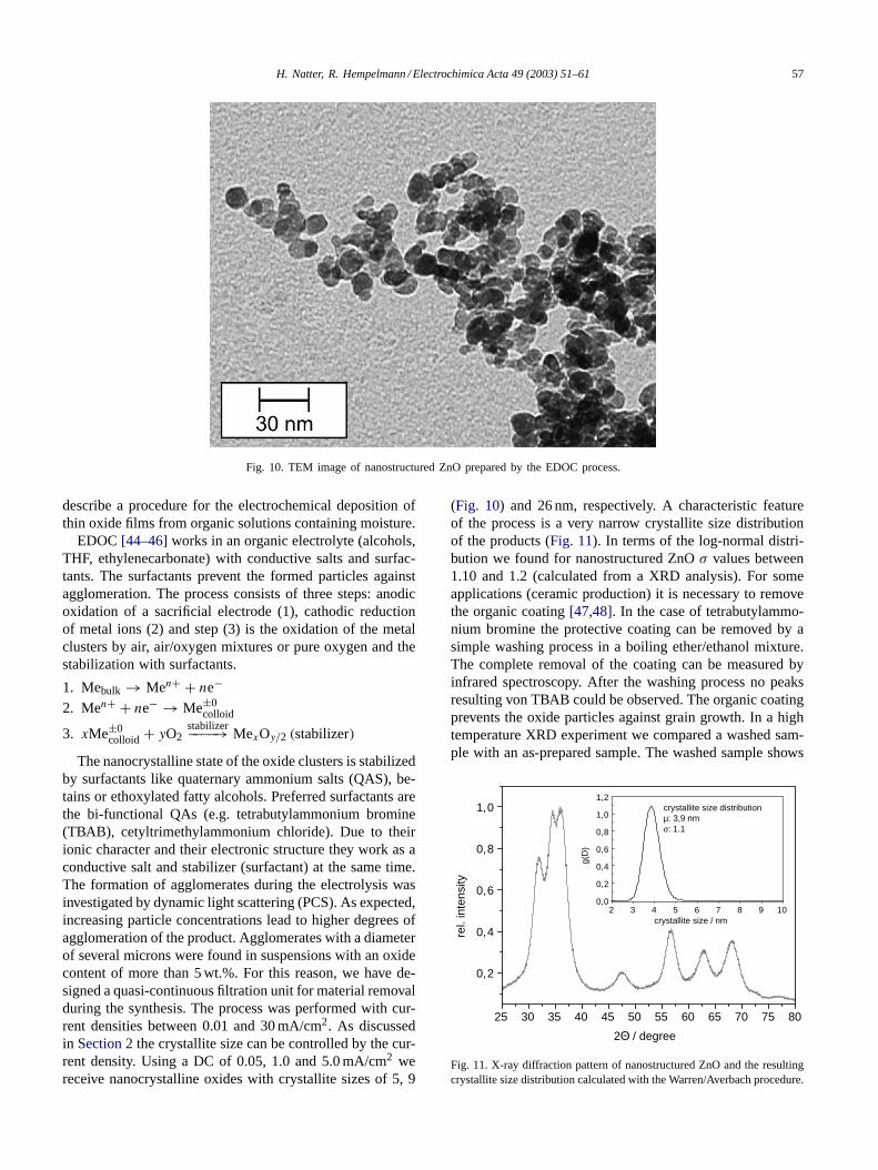
3. Electrochemical deposition under oxidizingconditions (EDOC)
Many preparation methods have been developed forthe preparation of nanostructured metal oxides: physi-
Fig. 9. Schematic representation of the EDOC process using sacrificial anodes as metal ion source.
cal methods (mechanical milling), gas-to-particle routes[40] (inert gas condensation, flame pyrolysis, chemicalvapour synthesis) as well as wet chemical techniques likesol–gel-procedures, microemulsions[41], coprecipitation,hydrothermal synthesis. Mechanical milling of polycrys-talline material leads within a short time to large amountsof nanomaterial, but the product is contaminated with impu-rities resulting from the milling device. The disadvantagesof gas-to-particle routes are expensive alcoxide-precursorsand equipments. Nano oxides prepared by precipitationmethods often show a broad crystallite size distributionsand contaminations with hydroxides or bases. A furtherproblem is the precipitation of mixed oxides because theconstants of solubility of the components are often differentand therefore the product is a simple mixture of the oxides.An alternative to all this procedures is the electrochemicalEDOC process which is a hybrid between a top down anda bottom up route. This procedure allows the preparationof nanostructured oxides (Fig. 9), mixed oxides and dopedoxides.
3.1. The process conception and experimental details
The EDOC process (Fig. 9) shows some similarity withan electrochemical synthesis procedure for small amountsof metallic catalyst particles[42] with diameters of severalnanometers which uses an organic electrolyte, however un-der strict exclusion of moisture and air. Pascal et al.[43]
H. Natter, R. Hempelmann / Electrochimica Acta 49 (2003) 51–61 57
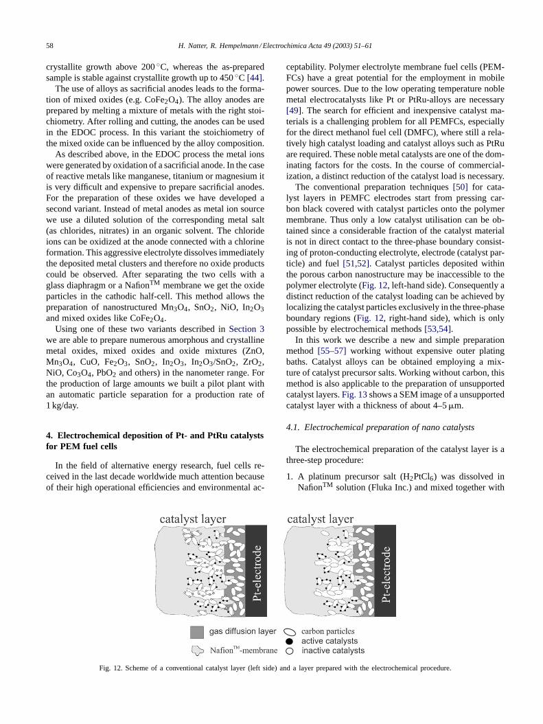
Fig. 10. TEM image of nanostructured ZnO prepared by the EDOC process.
describe a procedure for the electrochemical deposition ofthin oxide films from organic solutions containing moisture.
EDOC[44–46]works in an organic electrolyte (alcohols,THF, ethylenecarbonate) with conductive salts and surfac-tants. The surfactants prevent the formed particles againstagglomeration. The process consists of three steps: anodicoxidation of a sacrificial electrode (1), cathodic reductionof metal ions (2) and step (3) is the oxidation of the metalclusters by air, air/oxygen mixtures or pure oxygen and thestabilization with surfactants.
1. Mebulk → Men+ + ne−
2. Men+ + ne− → Me±0colloid
3. xMe±0colloid + yO2
stabilizer−−−−→ MexOy/2 (stabilizer)
The nanocrystalline state of the oxide clusters is stabilizedby surfactants like quaternary ammonium salts (QAS), be-tains or ethoxylated fatty alcohols. Preferred surfactants arethe bi-functional QAs (e.g. tetrabutylammonium bromine(TBAB), cetyltrimethylammonium chloride). Due to theirionic character and their electronic structure they work as aconductive salt and stabilizer (surfactant) at the same time.The formation of agglomerates during the electrolysis wasinvestigated by dynamic light scattering (PCS). As expected,increasing particle concentrations lead to higher degrees ofagglomeration of the product. Agglomerates with a diameterof several microns were found in suspensions with an oxidecontent of more than 5 wt.%. For this reason, we have de-signed a quasi-continuous filtration unit for material removalduring the synthesis. The process was performed with cur-rent densities between 0.01 and 30 mA/cm2. As discussedin Section 2the crystallite size can be controlled by the cur-rent density. Using a DC of 0.05, 1.0 and 5.0 mA/cm2 wereceive nanocrystalline oxides with crystallite sizes of 5, 9
(Fig. 10) and 26 nm, respectively. A characteristic featureof the process is a very narrow crystallite size distributionof the products (Fig. 11). In terms of the log-normal distri-bution we found for nanostructured ZnOσ values between1.10 and 1.2 (calculated from a XRD analysis). For someapplications (ceramic production) it is necessary to removethe organic coating[47,48]. In the case of tetrabutylammo-nium bromine the protective coating can be removed by asimple washing process in a boiling ether/ethanol mixture.The complete removal of the coating can be measured byinfrared spectroscopy. After the washing process no peaksresulting von TBAB could be observed. The organic coatingprevents the oxide particles against grain growth. In a hightemperature XRD experiment we compared a washed sam-ple with an as-prepared sample. The washed sample shows
25 30 35 40 45 50 55 60 65 70 75 80
0,2
0,4
0,6
0,8
1,0
2 3 4 5 6 7 8 9 100,0
0,2
0,4
0,6
0,8
1,0
1,2crystallite size distributionµ: 3,9 nmσ: 1.1
g(D
)
crystallite size / nm
rel.
inte
nsity
2Θ / degree
Fig. 11. X-ray diffraction pattern of nanostructured ZnO and the resultingcrystallite size distribution calculated with the Warren/Averbach procedure.
58 H. Natter, R. Hempelmann / Electrochimica Acta 49 (2003) 51–61
crystallite growth above 200◦C, whereas the as-preparedsample is stable against crystallite growth up to 450◦C [44].
The use of alloys as sacrificial anodes leads to the forma-tion of mixed oxides (e.g. CoFe2O4). The alloy anodes areprepared by melting a mixture of metals with the right stoi-chiometry. After rolling and cutting, the anodes can be usedin the EDOC process. In this variant the stoichiometry ofthe mixed oxide can be influenced by the alloy composition.
As described above, in the EDOC process the metal ionswere generated by oxidation of a sacrificial anode. In the caseof reactive metals like manganese, titanium or magnesium itis very difficult and expensive to prepare sacrificial anodes.For the preparation of these oxides we have developed asecond variant. Instead of metal anodes as metal ion sourcewe use a diluted solution of the corresponding metal salt(as chlorides, nitrates) in an organic solvent. The chlorideions can be oxidized at the anode connected with a chlorineformation. This aggressive electrolyte dissolves immediatelythe deposited metal clusters and therefore no oxide productscould be observed. After separating the two cells with aglass diaphragm or a NafionTM membrane we get the oxideparticles in the cathodic half-cell. This method allows thepreparation of nanostructured Mn3O4, SnO2, NiO, In2O3and mixed oxides like CoFe2O4.
Using one of these two variants described inSection 3we are able to prepare numerous amorphous and crystallinemetal oxides, mixed oxides and oxide mixtures (ZnO,Mn3O4, CuO, Fe2O3, SnO2, In2O3, In2O3/SnO2, ZrO2,NiO, Co3O4, PbO2 and others) in the nanometer range. Forthe production of large amounts we built a pilot plant withan automatic particle separation for a production rate of1 kg/day.
4. Electrochemical deposition of Pt- and PtRu catalystsfor PEM fuel cells
In the field of alternative energy research, fuel cells re-ceived in the last decade worldwide much attention becauseof their high operational efficiencies and environmental ac-
Fig. 12. Scheme of a conventional catalyst layer (left side) and a layer prepared with the electrochemical procedure.
ceptability. Polymer electrolyte membrane fuel cells (PEM-FCs) have a great potential for the employment in mobilepower sources. Due to the low operating temperature noblemetal electrocatalysts like Pt or PtRu-alloys are necessary[49]. The search for efficient and inexpensive catalyst ma-terials is a challenging problem for all PEMFCs, especiallyfor the direct methanol fuel cell (DMFC), where still a rela-tively high catalyst loading and catalyst alloys such as PtRuare required. These noble metal catalysts are one of the dom-inating factors for the costs. In the course of commercial-ization, a distinct reduction of the catalyst load is necessary.
The conventional preparation techniques[50] for cata-lyst layers in PEMFC electrodes start from pressing car-bon black covered with catalyst particles onto the polymermembrane. Thus only a low catalyst utilisation can be ob-tained since a considerable fraction of the catalyst materialis not in direct contact to the three-phase boundary consist-ing of proton-conducting electrolyte, electrode (catalyst par-ticle) and fuel[51,52]. Catalyst particles deposited withinthe porous carbon nanostructure may be inaccessible to thepolymer electrolyte (Fig. 12, left-hand side). Consequently adistinct reduction of the catalyst loading can be achieved bylocalizing the catalyst particles exclusively in the three-phaseboundary regions (Fig. 12, right-hand side), which is onlypossible by electrochemical methods[53,54].
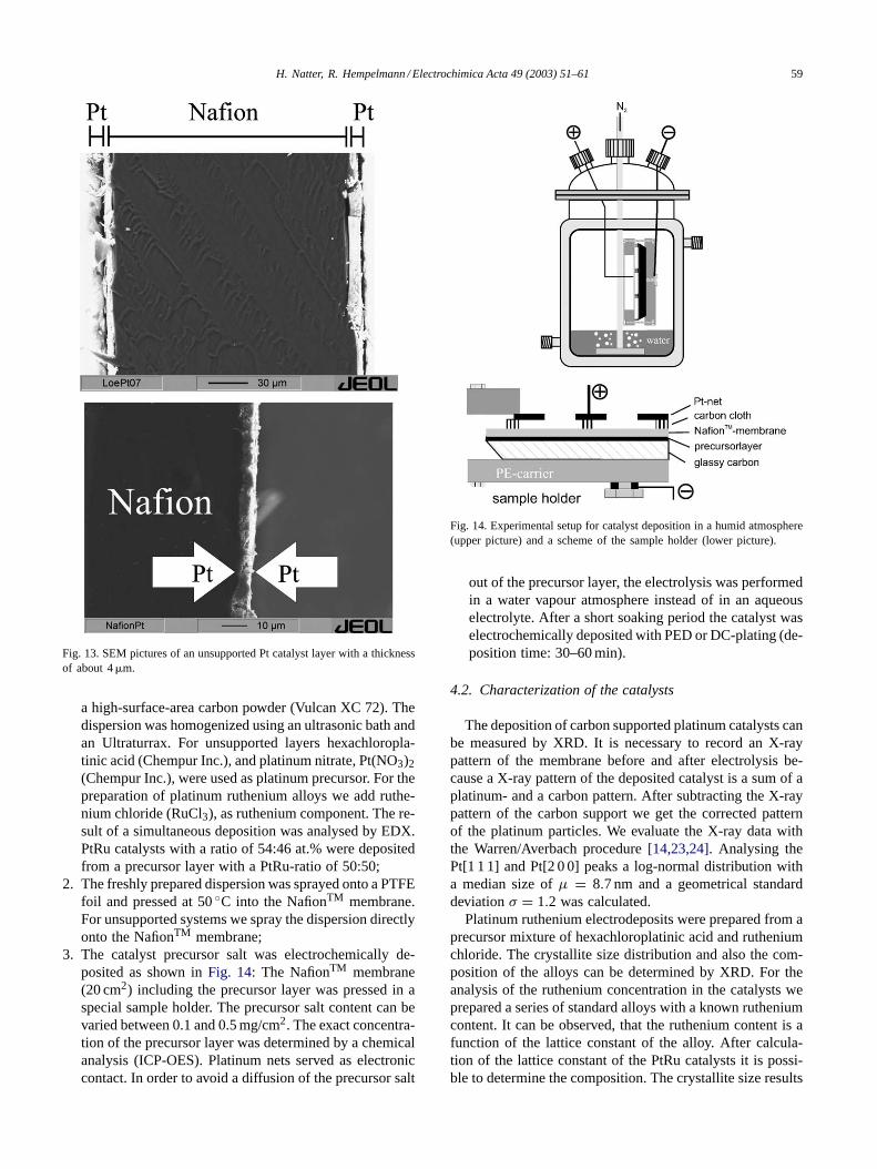
In this work we describe a new and simple preparationmethod[55–57] working without expensive outer platingbaths. Catalyst alloys can be obtained employing a mix-ture of catalyst precursor salts. Working without carbon, thismethod is also applicable to the preparation of unsupportedcatalyst layers.Fig. 13shows a SEM image of a unsupportedcatalyst layer with a thickness of about 4–5�m.
4.1. Electrochemical preparation of nano catalysts
The electrochemical preparation of the catalyst layer is athree-step procedure:
1. A platinum precursor salt (H2PtCl6) was dissolved inNafionTM solution (Fluka Inc.) and mixed together with
H. Natter, R. Hempelmann / Electrochimica Acta 49 (2003) 51–61 59
Fig. 13. SEM pictures of an unsupported Pt catalyst layer with a thicknessof about 4�m.
a high-surface-area carbon powder (Vulcan XC 72). Thedispersion was homogenized using an ultrasonic bath andan Ultraturrax. For unsupported layers hexachloropla-tinic acid (Chempur Inc.), and platinum nitrate, Pt(NO3)2(Chempur Inc.), were used as platinum precursor. For thepreparation of platinum ruthenium alloys we add ruthe-nium chloride (RuCl3), as ruthenium component. The re-sult of a simultaneous deposition was analysed by EDX.PtRu catalysts with a ratio of 54:46 at.% were depositedfrom a precursor layer with a PtRu-ratio of 50:50;
2. The freshly prepared dispersion was sprayed onto a PTFEfoil and pressed at 50◦C into the NafionTM membrane.For unsupported systems we spray the dispersion directlyonto the NafionTM membrane;
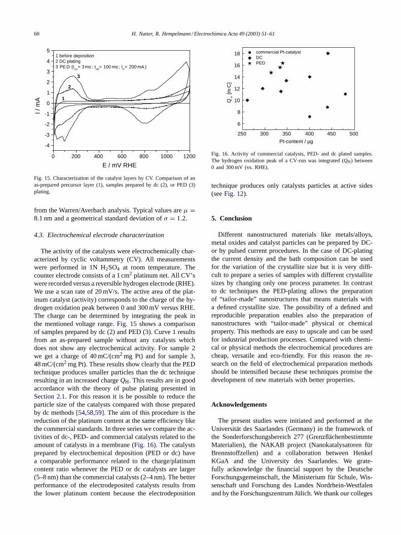
3. The catalyst precursor salt was electrochemically de-posited as shown inFig. 14: The NafionTM membrane(20 cm2) including the precursor layer was pressed in aspecial sample holder. The precursor salt content can bevaried between 0.1 and 0.5 mg/cm2. The exact concentra-tion of the precursor layer was determined by a chemicalanalysis (ICP-OES). Platinum nets served as electroniccontact. In order to avoid a diffusion of the precursor salt
Fig. 14. Experimental setup for catalyst deposition in a humid atmosphere(upper picture) and a scheme of the sample holder (lower picture).
out of the precursor layer, the electrolysis was performedin a water vapour atmosphere instead of in an aqueouselectrolyte. After a short soaking period the catalyst waselectrochemically deposited with PED or DC-plating (de-position time: 30–60 min).
4.2. Characterization of the catalysts
The deposition of carbon supported platinum catalysts canbe measured by XRD. It is necessary to record an X-raypattern of the membrane before and after electrolysis be-cause a X-ray pattern of the deposited catalyst is a sum of aplatinum- and a carbon pattern. After subtracting the X-raypattern of the carbon support we get the corrected patternof the platinum particles. We evaluate the X-ray data withthe Warren/Averbach procedure[14,23,24]. Analysing thePt[1 1 1] and Pt[2 0 0] peaks a log-normal distribution witha median size ofµ = 8.7 nm and a geometrical standarddeviationσ = 1.2 was calculated.
Platinum ruthenium electrodeposits were prepared from aprecursor mixture of hexachloroplatinic acid and rutheniumchloride. The crystallite size distribution and also the com-position of the alloys can be determined by XRD. For theanalysis of the ruthenium concentration in the catalysts weprepared a series of standard alloys with a known rutheniumcontent. It can be observed, that the ruthenium content is afunction of the lattice constant of the alloy. After calcula-tion of the lattice constant of the PtRu catalysts it is possi-ble to determine the composition. The crystallite size results
60 H. Natter, R. Hempelmann / Electrochimica Acta 49 (2003) 51–61
0 200 400 600 800 1000 1200
-4
-3
-2
-1
0
1
2
3
4
5
3
2
1
I / m
A
E / mV RHE
1 before deposition2 DC plating 3 PE D (t
on= 3 ms ; t
off= 100 ms ; I
P= 200 mA )
Fig. 15. Characterization of the catalyst layers by CV. Comparison of anas-prepared precursor layer (1), samples prepared by dc (2), or PED (3)plating.
from the Warren/Averbach analysis. Typical values areµ =8.1 nm and a geometrical standard deviation ofσ = 1.2.
4.3. Electrochemical electrode characterization
The activity of the catalysts were electrochemically char-acterized by cyclic voltammetry (CV). All measurementswere performed in 1N H2SO4 at room temperature. Thecounter electrode consists of a 1 cm2 platinum net. All CV’swere recorded versus a reversible hydrogen electrode (RHE).We use a scan rate of 20 mV/s. The active area of the plat-inum catalyst (activity) corresponds to the charge of the hy-drogen oxidation peak between 0 and 300 mV versus RHE.The charge can be determined by integrating the peak inthe mentioned voltage range.Fig. 15 shows a comparisonof samples prepared by dc (2) and PED (3). Curve 1 resultsfrom an as-prepared sample without any catalysts whichdoes not show any electrochemical activity. For sample 2we get a charge of 40 mC/(cm2 mg Pt) and for sample 3,48 mC/(cm2 mg Pt). These results show clearly that the PEDtechnique produces smaller particles than the dc techniqueresulting in an increased chargeQH. This results are in goodaccordance with the theory of pulse plating presented inSection 2.1. For this reason it is be possible to reduce theparticle size of the catalysts compared with those preparedby dc methods[54,58,59]. The aim of this procedure is thereduction of the platinum content at the same efficiency likethe commercial standards. In three series we compare the ac-tivities of dc-, PED- and commercial catalysts related to theamount of catalysts in a membrane (Fig. 16). The catalystsprepared by electrochemical deposition (PED or dc) havea comparable performance related to the charge/platinumcontent ratio whenever the PED or dc catalysts are larger(5–8 nm) than the commercial catalysts (2–4 nm). The betterperformance of the electrodeposited catalysts results fromthe lower platinum content because the electrodeposition
250 300 350 400 450 500
6
8
10
12
14
16
18 commercial Pt-catalyst DC PED
QH [m
C]
Pt-content / µg
Fig. 16. Activity of commercial catalysts, PED- and dc plated samples.The hydrogen oxidation peak of a CV-run was integrated (QH) between0 and 300 mV (vs. RHE).
technique produces only catalysts particles at active sides(seeFig. 12).
5. Conclusion
Different nanostructured materials like metals/alloys,metal oxides and catalyst particles can be prepared by DC-or by pulsed current procedures. In the case of DC-platingthe current density and the bath composition can be usedfor the variation of the crystallite size but it is very diffi-cult to prepare a series of samples with different crystallitesizes by changing only one process parameter. In contrastto dc techniques the PED-plating allows the preparationof “tailor-made” nanostructures that means materials witha defined crystallite size. The possibility of a defined andreproducible preparation enables also the preparation ofnanostructures with “tailor-made” physical or chemicalproperty. This methods are easy to upscale and can be usedfor industrial production processes. Compared with chemi-cal or physical methods the electrochemical procedures arecheap, versatile and eco-friendly. For this reason the re-search on the field of electrochemical preparation methodsshould be intensified because these techniques promise thedevelopment of new materials with better properties.
Acknowledgements
The present studies were initiated and performed at theUniversität des Saarlandes (Germany) in the framework ofthe Sonderforschungsbereich 277 (GrenzflächenbestimmteMaterialien), the NAKAB project (Nanokatalysatoren fürBrennstoffzellen) and a collaboration between HenkelKGaA and the University des Saarlandes. We grate-fully acknowledge the financial support by the DeutscheForschungsgemeinschaft, the Ministerium für Schule, Wis-senschaft und Forschung des Landes Nordrhein-Westfalenand by the Forschungszentrum Jülich. We thank our colleges
H. Natter, R. Hempelmann / Electrochimica Acta 49 (2003) 51–61 61
in the SFB and from the NAKAB project for stimulationdiscussions, in particular Dr. M. Schmelzer, A. Dierstein,M.-S. Löffler, Dr. J. Divisek, Dr. K. Wippermann, Dr. J.Mergel, Prof. J.-W. Schultze, Dr. U. König, Dr. C.E. Krill,Prof. R. Birringer, Dr. Krajewsky, Dr. H. Wolf, Z. Guan andProf. Th. Wichert.
References
[1] K.I. Popov, M.G. Pavlovic, Mod. Aspects Electrochem. 24 (1993)299.
[2] M. El-Sherik, U. Erb, J. Mater. Sci. 30 (1995) 5743.[3] A. Robertson, U. Erb, G. Palumbo, Nanostr. Mater 12 (1999) 1035.[4] H. Gleiter, Prog. Mater. Sci. 33 (1989) 223.[5] N. Wang, et al., Acta Met. 43 (1995) 519.[6] B. Szpunar, et al., Phys. Rev. B 53 (1996) 5547.[7] S. Wang, et al., Electrochem. Soc. Proc. 95–8 (1995) 244.[8] US Patent 5,516,415 (May 1996).[9] US Patent 5,538,615 (July 1996).
[10] H. Natter, R. Hempelmann, J. Phys. Chem. 100 (1996) 19525.[11] A.M. Alfantazi, U. Erb, J. Mater. Sci. Lett. 15 (1996) 1361.[12] J.C. Puippe, F. Leaman (Eds.), Theory and Practice of Pulse Plating,
Am. Electroplaters Soc., Florida, 1986.[13] E. Budevski, G. Staikov, J.W. Lorenz, Electrochemical Phase Trans-
formation and Growth, VCH, Weinheim, 1996, p. 161.[14] H. Natter, M. Schmelzer, M.-S. Löffler, C.E. Krill, A. Fitch, R.
Hempelmann, J. Phys. Chem. 104 (2000) 2467.[15] H. Natter, M. Schmelzer, R. Hempelmann, J. Mater. Res. 13 (1998)
1186.[16] H. Natter, T. Krajewski, R. Hempelmann, Ber. Bunsenges. Phys.
Chem. 100 (1996) 55.[17] H. Fischer, Elektrolytische Abscheidung und Elektrokristallisation
von Metallen, Herausg. W. Köster, Springer, Berlin/Göttingen/Heidelberg, 1954.
[18] A.S. Edelstein, R.C. Cammaratu (Eds.), Nanomaterials: Synthesis,Properties and Applications, IOP, Bristol, 1996.
[19] J.H. Fendler (Ed.), Nanoparticles and Nanostructured Films, Wiley–VCH, Weinheim, 1998.
[20] J.O’M. Bockris, G.A. Razumney, Fundamental Aspects of Electro-crystallization, Plenum Press, New York, 1967.
[21] B.E. Warren, L.E. Averbach, J. Appl. Phys. 21 (1950) 536.[22] B.E. Warren, L.E. Averbach, J. Appl. Phys. 23 (1952) 497.[23] B.E. Warren, X-ray diffraction, Dover, New York, 1990.[24] C.E. Krill, R. Birringer, Phil. Mag. A 77 (1998) 621.[25] K.D. Baker, H. Schneider, US Patent 4,435,253 (1984).[26] T. Fearn, GB Patent 2266 (1871).[27] C. Cheung, G. Palumbo, U. Erb, Scr. Metal. Et. Mater. 23 (1989)
1679.
[28] A. Brenner, Electrodeposition of Alloys, vol. 3, Academic Press,New York, 1963.
[29] T.M. Harris, J.S. Clair, J. Electrochem. Soc. 143 (1996) 245.[30] S. Hessami, C.W. Tobias, J. Electrochem. Soc. 136 (1989) 3611.[31] R. Przenioslo, R. Winter, H. Natter, M. Schmelzer, R. Hempelmann,
W. Wagner, Phys. Rev. B 63 (2001) 54408.[32] H. Natter, M. Schmelzer, S. Janssen, R. Hempelmann, Ber. Bunsen-
ges. Phys. Chem. 101 (1997) 1706.[33] R. Przenioslo, J. Wagner, H. Natter, R. Hempelmann, W. Wagner, J.
Alloys Compounds 328 (2001) 259.[34] L.E. Candlish, B.H. Kear, B.H. Kim, Nanostr. Mater. 1 (1992) 119.[35] M.J. Aus, B. Szpunar, U. Erb, A.M. El-Sherik, J. Appl. Phys. 75
(1994) 3632.[36] W. Gong, H. Li, Z. Zhao, J. Chen, J. Appl. Phys. 69 (1991) 5119.[37] S. Janssen, H. Natter, R. Hempelmann, Swiss Neutron News 11
(1997) 27.[38] K. Boylan, D. Ostrander, U. Erb, G. Palumbo, K.T. Aust, Scr. Metal.
et Mater. 25 (1991) 2711.[39] H. Natter, M.-S. Löffler, C.E. Krill, R. Hempelmann, Scr. Mater. 44
(2001) 2321.[40] H. Hahn, Nanostruct. Mater. 9 (1997) 3.[41] H. Herrig, R. Hempelmann, Mater. Lett. 27 (1996) 287.[42] M. Reetz, German Patent DE 44,08,512 A1.[43] C. Pascal, J.L. Pascal, F. Favier, M.L. Elidrisi-Moubtassim, C. Payer,
Chem. Mater. 11 (1999) 141.[44] A. Dierstein, H. Natter, F. Meier, H.-O. Stephan, Ch. Kropf, R.
Hempelmann, Scr. Mater. 44 (2001) 2209.[45] H. Natter, R. Hempelmann, German Patent DE 198,40,842 A1 (2000).[46] H. Natter, A. Dierstein, R. Hempelmann, H.-O. Stephan, C. Kropf
WO 0261183 A2 (2002).[47] R. Rüffler, R. Clasen, H. Natter, A. Dierstein, R. Hempelmann,
Ceram. Trans. 115 (2000) 293.[48] R. Rüffler, R. Clasen, H. Natter, A. Dierstein, R. Hempelmann,
Ceram. Trans. 115 (2000) 623.[49] H. Wendt, M. Götz, Chemie unserer Zeit 6 (1997) 301.[50] P. Stoneheart, Ber. Bunsenges. Phys. Chem. 94 (1990) 913.[51] J. McBreen, J. Electrochem. Soc. 132 (1985) 112.[52] S.D. Thompson, L.R. Jordan, M. Forsyth, Electrochim. Acta 46
(2001) 1657.[53] S. Srubuvasab, O.A. Velev, A. Parthasarathy, D.J. Manko, A.J. Ap-
pleby, NASA Conf. Publication 3125 (1989) 11.[54] E.J. Taylor, E.B. Anderson, N.R.K. Vilambi, J. Electrochem. Soc.
139 (1992) 45.[55] M.-S. Löffler, B. Groß, H. Natter, R. Hempelmann, T. Krajewski, J.
Divisek, PCCP 3 (2001) 333.[56] M.-S. Löffler, B. Groß, H. Natter, R. Hempelmann, T. Krajewski, J.
Divisek, Scripta Mater. 44 (2001) 2253.[57] R. Hempelmann, M.-S. Löffler, H. Natter, H. Schmitz, J. Divisek,
PZT Patent WO 0213301.[58] J. Niebling, K. Gorgos, US Patent 5,084,144 (1992).[59] M.W. Verbrugge, J. Electrochem. Soc. 141 (1994) 46.