table of contents 2013 ieee conference on e...
TRANSCRIPT
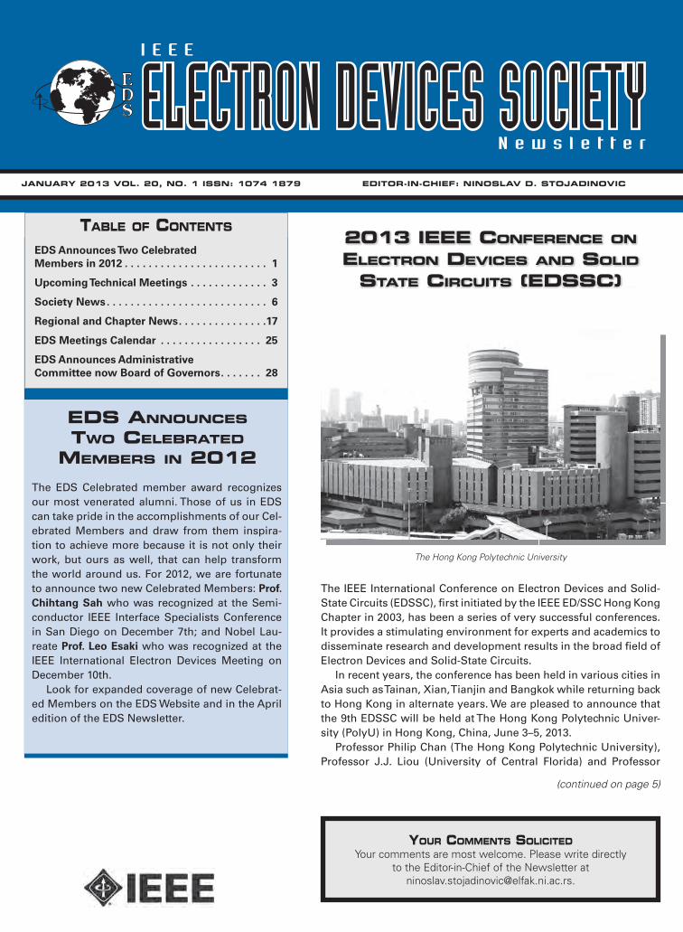
The IEEE International Conference on Electron Devices and Solid-
State Circuits (EDSSC), first initiated by the IEEE ED/SSC Hong Kong
Chapter in 2003, has been a series of very successful conferences.
It provides a stimulating environment for experts and academics to
disseminate research and development results in the broad field of
Electron Devices and Solid-State Circuits.
In recent years, the conference has been held in various cities in
Asia such as Tainan, Xian, Tianjin and Bangkok while returning back
to Hong Kong in alternate years. We are pleased to announce that
the 9th EDSSC will be held at The Hong Kong Polytechnic Univer-
sity (PolyU) in Hong Kong, China, June 3–5, 2013.
Professor Philip Chan (The Hong Kong Polytechnic University),
Professor J.J. Liou (University of Central Florida) and Professor
JANUARY 2013 VOL. 20, NO. 1 ISSN: 1074 1879 EDITOR-IN-CHIEF: NINOSLAV D. STOJADINOVIC
TABLE OF CONTENTS
EDS Announces Two Celebrated Members in 2012 . . . . . . . . . . . . . . . . . . . . . . . . 1
Upcoming Technical Meetings . . . . . . . . . . . . . 3
Society News . . . . . . . . . . . . . . . . . . . . . . . . . . . 6
Regional and Chapter News . . . . . . . . . . . . . . .17
EDS Meetings Calendar . . . . . . . . . . . . . . . . . 25
EDS Announces Administrative Committee now Board of Governors . . . . . . . 28
2013 IEEE CONFERENCE ON ELECTRON DEVICES AND SOLID
STATE CIRCUITS (EDSSC)
The EDS Celebrated member award recognizes
our most venerated alumni. Those of us in EDS
can take pride in the accomplishments of our Cel-
ebrated Members and draw from them inspira-
tion to achieve more because it is not only their
work, but ours as well, that can help transform
the world around us. For 2012, we are fortunate
to announce two new Celebrated Members: Prof. Chihtang Sah who was recognized at the Semi-
conductor IEEE Interface Specialists Conference
in San Diego on December 7th; and Nobel Lau-
reate Prof. Leo Esaki who was recognized at the
IEEE International Electron Devices Meeting on
December 10th.
Look for expanded coverage of new Celebrat-
ed Members on the EDS Website and in the April
edition of the EDS Newsletter.
EDS ANNOUNCES TWO CELEBRATED
MEMBERS IN 2012
(continued on page 5)
The Hong Kong Polytechnic University
YOUR COMMENTS SOLICITEDYour comments are most welcome. Please write directly
to the Editor-in-Chief of the Newsletter at [email protected].
2 IEEE Electron Devices Society Newsletter ❍ January 2013
ELECTRON DEVICES
SOCIETY
NEWSLETTER
EDITORIAL STAFF
PresidentPaul K.L. YuUniv. of California at San DiegoE-mail: [email protected]
President-Elect Albert Z.H. WangUniversity of California, RiversideE-mail: [email protected]
TreasurerRavi M. TodiIBM MicroelectronicsE-mail: [email protected]
SecretaryFernando GuarinIBM MicroelectronicsE-mail: [email protected]
Jr. Past PresidentRenuka P. JindalUniversity of Louisiana at LafayetteE-mail: [email protected]
Sr. Past PresidentCor L. ClaeysIMECE-mail: [email protected]
Vice-President of AwardsMarvin H. WhiteOhio State UniversityE-mail: [email protected]
Vice-President of Educational ActivitiesMeyya MeyyappanNASA Ames Research CenterE-mail: [email protected]
Vice-President of ConferencesBin ZhaoFairchild SemiconductorE-mail: [email protected]
Vice President of MembershipJamal DeenMcMaster UniversityE-Mail: [email protected]
Vice-President of PublicationsSamar SahaSuVolta, Inc.E-mail: [email protected]
Vice-President of Regions/ChaptersXing ZhouNanyang Technological University E-Mail: [email protected]
Vice-President of Technical ActivitiesJoachim N. BurghartzIMS ChipsE-Mail: [email protected]
IEEE NewslettersTheresa SmithIEEE Operations CenterE-mail: [email protected]
Executive DirectorChristopher JannuzziIEEE Operations CenterE-mail: [email protected]
Membership AdministratorJoyce Aqara (Lombardini)IEEE Operations CenterE-mail: [email protected]
IEEE prohibits discrimination, harassment, and bullying. For more information, visit http://www.ieee.org/web/aboutus/whatis/policies/p9-26.html.
IEEE Electron Devices Society Newsletter (ISSN 1074 1879) is published quarterly by the Electron Devices Society of the Institute of Electrical and Electronics Engineers, Inc. Headquarters: 3 Park Avenue, 17th Floor, New York, NY 10016-5997. Printed in the U.S.A. One dollar ($1.00) per member per year is included in the Society fee for each member of the Electron Devices Society. Periodicals postage paid at New York, NY and at additional mailing offices. Postmaster: Send address changes to IEEE Electron Devices Society Newsletter, IEEE, 445 Hoes Lane, Piscataway, NJ 08854.
Copyright © 2013 by IEEE: Information contained in this Newsletter may be copied without permission provided that copies are not used or distributed for direct commercial advantage, and the title of the publication and its date appear on each photocopy.
Editor-In-ChiefNinoslav D. StojadinovicUniversity of NisE-mail: [email protected]
REGIONS 1-6, 7 & 9Eastern, Northeastern & South-eastern USA (Regions 1,2 & 3)Fernando GuarinIBM MicroelectronicsE-mail: [email protected]
Central USA & Canada(Regions 4 & 7)Peyman ServatiUniversity of British ColumbiaE-mail: [email protected]
Southwestern & Western USA(Regions 5 & 6)Adam M. ConwayLawrence Livermore Nat. Lab.E-mail: [email protected]
Latin America (Region 9)Francisco J. Garcia SanchezUniversity Simon BolivarE-mail: [email protected]
REGION 8Eastern Europe & the former Soviet UnionTomislav SuligojUniversity of ZagrebE-mail: [email protected]
Scandinavia & Central EuropeZygmunt CiotaTechnical University of LodzE-mail: [email protected]
UK, Middle East & AfricaJonathan TerryThe University of EdinburghE-mail: [email protected]
Western EuropeJan VobeckyAbb Switzerland Ltd.E-mail: [email protected]
REGION 10Australia, New Zealand & South AsiaM.K. RadhakrishnanNanoRelE-mail: [email protected]
Northeast AsiaKuniyuki KakushimaTokyo Institute of TechnologyE-mail: [email protected]
East AsiaMansun J. ChanHong Kong Univ. of Sc. & Tech.E-mail: [email protected]
CONTRIBUTIONS WELCOME
Readers are encouraged to submit news items concerning the Society and its members. Please send your ideas/articles directly to either the Editor-in-Chief or appropriate Editor. The e-mail addresses of these individuals are listed on this page. Whenever possible, e-mail is the preferred form of submission. NEWSLETTER DEADLINES
ISSUE DUE DATE
January October 1st April January 1st July April 1st October July 1st
The EDS Newsletter archive can be found on the Society web site at http://eds.ieee.org/eds-newsletters.html. The archive contains issues from July 1994 to the present.
EDS AdComElected Members-at-Large
Elected for a three-year term (maximum two terms) with ‘full’ voting privileges
2013 TERM 2014 TERM 2015 TERM
A. Escobosa (1) Z. Celik-Butler (1) Daniel Camacho (1)J. J. Liou (1) M. Chan (1) Subramanian S. Iyer (2)M. Ostling (1) S. Chung (1) Meyya Meyyappan (2)M.K. Radhakrishnan (1) S. Deleonibus (2) Arokia Nathan (2)R. M. Todi (2) F. Guarin (2) Michael Shur (2)A. Z.H. Wang (1) T.L. Ren (1) Doug Verret (1)X. Zhou (1) S. Saha (2) Bin Zhao (2) E. Sangiorgi (1)
January 2013 ❍ IEEE Electron Devices Society Newsletter 3
2013 IEEE INTERNATIONAL RELIABILITY PHYSICS SYMPOSIUM (IRPS)
U P C O M I N G T E C H N I C A L M E E T I N G S
The IEEE International Reliability
Physics Symposium (IRPS) is the
world’s premier forum for leading-
edge research addressing devel-
opments in the Reliability Physics
of devices, materials, circuits, and
products. IRPS is the conference
where emerging Reliability Physics challenges and possible solutions to
achieve realistic End-of-Life projec-
tions are first discussed. This year,
the IRPS will be held at Hyatt Regen-
cy Monterey Resort & Spa in Mon-
terey, California, USA. Scheduled for
April 16–18, 2013, the IRPS will com-
mence with two full days of tutorials
and year-in-review on Sunday, April
14th and Monday, April 15th.
The IRPS draws presentations and
attendees from industry, academia
and governmental agencies world-
wide. No other meeting presents
as much leading work in so many
different areas of reliability of elec-
tronic devices, encompassing silicon
device, non-silicon device, process
technology, nanotechnology, opto-
electronics, photovoltaic and MEMS
technology.
For the IRPS 2013, we are empha-
sizing Reliability Compact Modelingand Circuit Simulation with sub-top-
ics such as methodologies for reliabil-
ity simulation, reliability simulator
calibration and checkers. We are also
emphasizing Electronic Systems reli-ability comprehending complex ap-
plications such as automotive, space,
communications, medical, screening
techniques and system monitoring.
IRPS 2013 will also feature in-
creased participation in the fields of
Advanced CMOS scaling, GaN, new
materials introduction, new pro-
cesses or integration strategies, and/
or fundamentally new device archi-
tectures. The conference will offer a
full slate of tutorials, evening panel
debates and workshops, invited ple-
nary talks in addition to an outstand-ing technical program.
The hotel is located in Monterey’s
downtown which is one of the more
beautiful coastal cities of California.
Today, Montery is most commonly
known for its beautiful coastline, its
world-class aquarium and from the
many John Steinbeck novels that
used the town as their setting includ-
ing Cannery Row and Tortilla Flat.
IRPS consists of three days (Tues–
Thurs, April 16–18) of plenary and
parallel technical sessions present-
ing original, state-of-the-art work.
Other opportunities at the sympo-
sium include:
• Two-Day Tutorial Program (Sunday–Monday April 14–15).
The IRPS tutorial program is a
comprehensive two-day event de-
signed to help both the new engi-
neer and experienced researcher.
The tutorial program contains
both beginner and expert tracks,
and is broken down into topic
areas that allow the attendee to
participate in tutorials relevant to
their work with minimum conflicts
between subject areas.
• Year in Review Session (Monday
April 15). These seminars provide
a summary of the most signifi-
cant developments in the reliabil-
ity community over the past year.
This serves as a convenient, single
source of information for attend-
ees to keep current with the recent
reliability literature. Industry ex-
perts serve as the “tour guide” and
save you time by collecting and
summarizing this information to
bring you up to date in a particular
area as efficiently as possible.
• Evening Poster Session. The
poster session will provide an ad-
ditional opportunity for authors
to present their original research.
The setting is informal and al-
lows for easy discussion between
authors and other attendees.
• Evening Session Workshops.
These workshops enhance the
symposium by providing the at-
tendees an opportunity to meet
in informal groups to discuss key
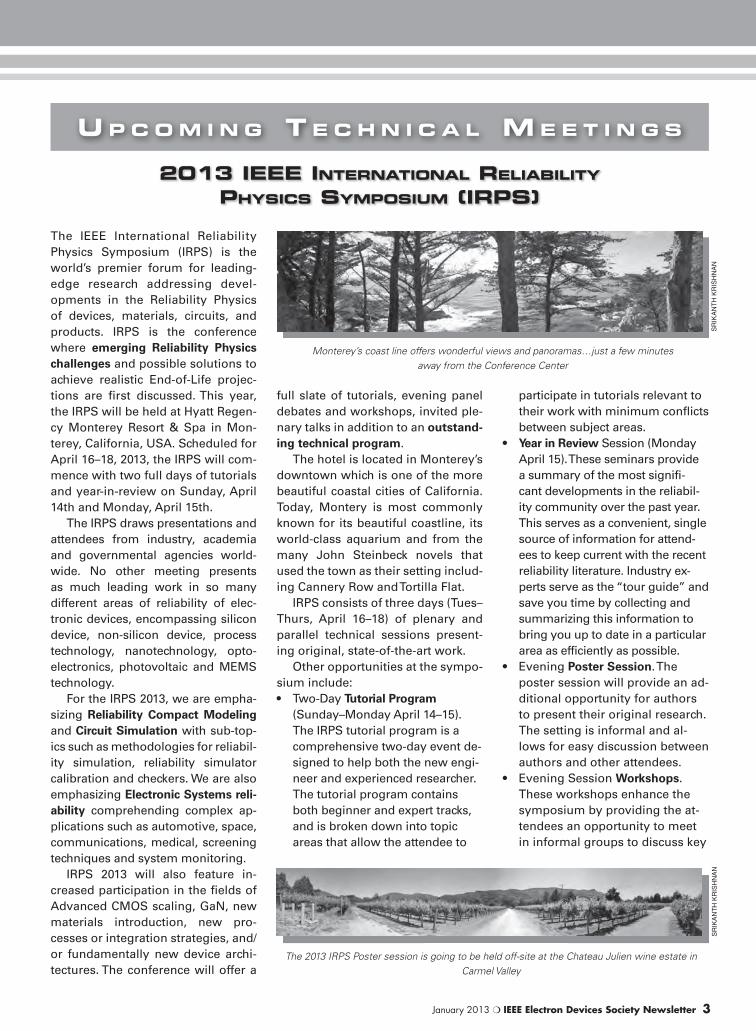
Monterey’s coast line offers wonderful views and panoramas…just a few minutes away from the Conference Center
SR
IKA
NT
H K
RIS
HN
AN
The 2013 IRPS P oster session is going to be held off-site at the Chateau Julien wine estate in Carmel Valley
SR
IKA
NT
H K
RIS
HN
AN
4 IEEE Electron Devices Society Newsletter ❍ January 2013
reliability physics topics with the
guidance of experienced mod-
erators. Some of the workshop
topics are directly coupled to the
technical program to provide a
venue for more discussion on
the topic.
• Vendor Exhibits. Held in paral-
lel with the technical sessions, the
equipment demonstrations pro-
vide a forum for manufacturers of
state-of-the-art laboratory equip-
ment to present their products.
Attendees are encouraged to visit
the manufacturers’ booths for in-
formation and demonstrations.
• IRPS Paper Awards. IRPS bestows
awards for Best Paper, Outstand-
ing Paper, Best Poster and Best
Student Talk. The Best Paper au-
thor is typically invited to present
the paper at ESREF in October.
• As part of our emphasis on Re-
liability Compact Modeling and
Circuit Simulation, we have ar-
ranged with the Compact Mod-eling Council to co-locate their
quarterly standards meeting
(on April 18,19) along with us in
Monterey for the first time ever.
This will better enable IRPS par-
ticipation by the CMC’s compact
modeling and circuit simulation
experts, facilitating greater inter-
action between them and Reli-
ability experts.
For registration and other informa-
tion, visit the IRPS 2013 home page
at http://www.irps.org/. The IRPS
committee members look forward to
seeing you in April.
Vincent Huard
2013 IRPS Publicity Chair
STMicroelectronics
Srikanth Krishnan
2013 IRPS General Chair
Texas Instruments
2013 INTERNATIONAL CONFERENCE ON MICROELECTRONIC TEST STRUCTURES (ICMTS)
The 26th International Conference
on Microelectronic Test Structures
(ICMTS) will be held at Osaka Uni-
versity Nakanoshima Center, Osaka,
Japan, bringing together designers
and users of test structures to dis-
cuss recent developments and fu-
ture directions. The conference will
be held on March 26–28, 2013, pre-
ceded by a one-day Tutorial Short
Course on Microelectronic Test
Structures on March 25th. The con-
ference will be held in cooperation
with the Institute of Electronics, In-
formation and Communication En-
gineers, and the Japan Society of
Applied Physics and will be spon-
sored by the IEEE Electron Devices
Society, and the Association for Pro-
motion of Electrical, Electronic and
Information Engineering.
The ICMTS 2013 will consist of 42
papers in 10 oral sessions and there
will be an equipment exhibition relat-
ing to test structure measurements.
A test structure is key character-
ization vehicle for process develop-
ment, device development, circuit
design and its production and its
importance is increasing. ICMTS has
brought engineers and researchers
together to discuss recent develop-
ments and future directions of test
structure research over the past two
decades. Topics of ICMTS have been
expanded as semiconductor tech-
nologies and application advance.
The topics to be covered by the
technical program of the conference
include:
Material and Process Character-ization: Evaluation of high-k gate di-
electrics, resistivity, mobility, stress,
contact resistance, and interconnect
measurements.
Manufacturing of Integrated Cir-cuits and MEMS: Evaluation of in-
dividual and groups of integrated
circuits, device and MEMS process
steps and elements: transistors, di-
odes, mechanical structures, device
isolation, memory cells and inter-
connect. Assessment of MMICs, RF
components, 3D integration, and
multi chip packages.
MEMS and NEMS: Test structures
and methods for evaluating electro-
mechanical devices, such as actua-
tors, sensors, and switches devices,
and for evaluating nanosize and
unique device such as carbon nano-
tube transistor.
TSV technology for 3 D structure: Test structure for evaluating of TSV
process and layout dependence of
electrical characteristics.
Large Area Electronics and Emerg-ing Devices: Test structures for eval-
uating displays, printed / flexible de-
vices, power devices, photovoltaics,
as well as emerging devices, such as
organic / oxide-based / biomolecular
/ spintronic devices, ReRAMs, nano-
structures, and related materials.
Device and Circuit Modeling, Parameter Extraction: Model pa-
rameter extraction, RF device
modeling, de-embedding, pulsed
measurements, DC / AC / high fre-
quency measurement techniques,
and applications.
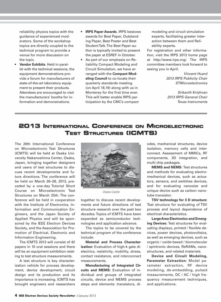
Osaka Castle
January 2013 ❍ IEEE Electron Devices Society Newsletter 5
Compact model for design: De-
velopment of compact model for
new device and phenomenon such
as organic device and variability of
MOSFET characteristics.
Noise characterization: Test struc-
ture and methods for characteriza-
tion and modeling of flicker noise,
random telegraph noise, and ther-
mal noise of MOSFET.
Reliability Test Structures: Test
structures and methods for transis-
tor / thin film / dielectric / intercon-
nect reliability evaluation, quality
assurance, thermal monitoring and
analysis, accelerated wafer level
tests, wafer level burn-in, and reli-
ability prediction.
Matching and Variability Test Structures: Test structure and meth-
ods for mismatch / variability char-
acterization and modeling of com-
ponents (transistors, resistors,
capacitors, inductors, mechanical
components) and circuits.
Yield Enhancement and Produc-tion Process Control: Yield enhance-
ment structures and methods, yield
modeling, statistical process control,
defect estimation structures and
methods, failure identification and
characterization, many-component /
matrix test circuitry for technology
assessment, evaluation of design-
manufacturing interactions (DFY).
Test Structure Design Methods: Design flows for automated design,
verification strategies, design for
analysis, parameterized design, and
related design issues.
Test Structure Utilization Strat-egy: Test equipment, probing and
programmable testing for process
diagnostics, test throughput opti-
mization, database and data analy-
sis methods, statistical data analy-
sis, expert systems, and related
techniques.
Osaka is easy to access from Osa-
ka and Kansai International Airports
by train and bus. It takes about 15
minutes to go to Osaka University
Nakanoshima Center by bus. This
famous city includes Osaka Castle
with its beautiful Golden Tea Room.
You will be able to enjoy some Osa-
ka foods and see many Cherry blos-
soms in March.
For registration and other infor-
mation, please visit the conference
website: http://www.if.t.u-tokyo.ac.jp/
ICMTS13/
The ICMTS committee members
look forward to seeing you in March
2013.
Tatsuya Ohguro
2013 ICMTS General Chairman
Toshiba Corporation
Yokohama, Japan
Paul Yu (University of California
at San Diego) are the Honorary
Chairs of the Conference and we are
pleased to receive tremendous sup-
port from our leading academia and
professionals all over the world.
The EDSSC 2013 marks a range
of related topics of interests, but
not limited to Analog Circuits; Bio-
medical Circuits; Digital and Mem-
ory Circuits; Memory Device and
Technology; RF & Microwave Cir-
cuits; Power Management Circuits;
Sensors, Imagers and MEMS; Data
Conversion Circuits; Wireless and
Wireline Communication Circuits;
Thin Gate Dielectrics; Device Reli-
ability; Energy Efficient Devices;
Emerging Devices; Nanoelectron-
ics; Organic Devices; Photonic De-
vices and RF & Microwave Devices.
Experts and academics in the broad
field of Electron Devices and Solid-
State Circuits are invited to share
their research and development
results. Professionals, scholars and
students from worldwide are called
on to participate.
2013 is the 10th Anniversary
of EDSSC and it marks a strategic
year for the conference. In collab-
oration with the Electron Devices
and Solid-State Circuits Societies,
it is shifted to the month of June
instead of December—an effort of
the ED/SSC Hong Kong Chapter to
work closer with the EDS and SSCS
headquarters by hosting the mid-
year EDS Board of Governors meet-
ing. In fact, the first EDSSC in 2003
was planned to be held in June, but
was postponed to December due to
the difficulty for speakers to travel
during the SARS period. We hope
the return to the initial schedule
will bring even greater successes to
EDSSC in the future.
For updates about the confer-
ence, please visit http://sites.ieee.
org/edssc2013. For inquiry, please e-
mail, [email protected].
Charles Surya
2013 EDSSC Co-Chair
The Hong Kong Polytechnic
University
Hong Kong, China
Philip Mok
2013 EDSSC Co-Chair
The Hong Kong University of
Science and Technology
Hong Kong, China
(continued from page 1)
2013 IEEE CONFERENCE ON ELECTRON DEVICES AND SOLID STATE CIRCUITS (EDSSC)
6 IEEE Electron Devices Society Newsletter ❍ January 2013
S O C I E T Y N E W S
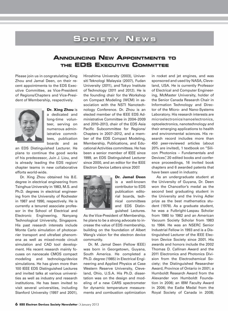
ANNOUNCING NEW APPOINTMENTS TO THE EDS EXECUTIVE COMMITTEE
Please join us in congratulating Xing
Zhou and Jamal Deen, on their re-
cent appointments to the EDS Exec-
utive Committee, as Vice-President
of Regions/Chapters and Vice-Presi-
dent of Membership, respectively.
Dr. Xing Zhou is
a dedicated and
long-time volun-
teer, serving on
numerous admin-
istrative commit-
tees, publication
boards and as
an EDS Distinguished Lecturer. He
plans to continue the good works
of his predecessor, Juin J. Liou, and
is already leading the EDS region/
chapter teams in new collaborative
efforts world-wide.
Dr. Xing Zhou obtained his B.E.
degree in electrical engineering from
Tsinghua University in 1983, M.S. and
Ph.D. degrees in electrical engineer-
ing from the University of Rochester
in 1987 and 1990, respectively. He is
currently a tenured associate profes-
sor in the School of Electrical and
Electronic Engineering, Nanyang
Technological University, Singapore.
His past research interests include
Monte Carlo simulation of photocar-
rier transport and ultrafast phenom-
ena as well as mixed-mode circuit
simulation and CAD tool develop-
ment. His recent research mainly fo-
cuses on nanoscale CMOS compact
modeling and technology/device
simulations. He has given more than
100 IEEE EDS Distinguished Lectures
and invited talks at various universi-
ties as well as industry and research
institutions. He has been invited to
visit several universities, including
Stanford University (1997 and 2001),
Hiroshima University (2003), Univer-
siti Teknologi Malaysia (2007), Fudan
University (2011), and Tokyo Institute
of Technology (2011 and 2012). He is
the founding chair for the Workshop
on Compact Modeling (WCM) in as-
sociation with the NSTI Nanotech-
nology Conference. Dr. Zhou is an
elected member of the IEEE EDS Ad-
ministrative Committee in 2004–2009
and 2010–2013, chair of the EDS Asia
Pacific Subcommittee for Regions/
Chapters in 2007–2012, and a mem-
ber of the EDS Compact Modeling,
Membership, Publications, and Edu-
cational Activities committees. He has
been a senior member of IEEE since
1999, an EDS Distinguished Lecturer
since 2000, and an editor for the IEEE
Electron Device Letters since 2007.
Dr. Jamal Deen
is a well-known
contributor to EDS
publication edito-
rial boards, tech-
nical committees
and EDS Distin-
guished Lectures.
As the Vice-President of Membership,
he plans to be a strong advocate to in-
crease the value of EDS membership,
building on the foundation of Albert
Wang’s vision for the electron device
community.
Dr. M. Jamal Deen (Fellow IEEE)
was born in Georgetown, Guyana,
South America. He completed a
Ph.D. degree (1985) in Electrical Engi-
neering and Applied Physics at Case
Western Reserve University, Cleve-
land, Ohio, U.S.A. His Ph.D. disser-
tation was on the design and mod-
eling of a new CARS spectrometer
for dynamic temperature measure-
ments and combustion optimization
in rocket and jet engines, and was
sponsored and used by NASA, Cleve-
land, USA. He is currently Professor
of Electrical and Computer Engineer-
ing, McMaster University, holder of
the Senior Canada Research Chair in
Information Technology and Direc-
tor of the Micro- and Nano-Systems
Laboratory. His research interests are
microelectronics/nanoelectronics,
optoelectronics, nanotechnology and
their emerging applications to health
and environmental sciences. His re-
search record includes more than
450 peer-reviewed articles (about
20% are invited), 1 textbook on “Sili-
con Photonics – Fundamentals and
Devices”, 20 edited books and confer-
ence proceedings, 16 invited book
chapters and 6 awarded patents that
have been used in industry.
As an undergraduate student at
the University of Guyana, Dr. Deen
won the Chancellor’s medal as the
second best graduating student in
the University and the Irving Adler
prize as the best mathematics stu-
dent (1978). As a graduate student,
he was a Fulbright-Laspau Scholar
from 1980 to 1982 and an American
Vacuum Society Scholar from 1983
to 1984. He was an NSERC Senior
Industrial Fellow in 1993 and is a Dis-
tinguished Lecturer of the IEEE Elec-
tron Device Society since 2001. His
awards and honors include the 2002
Thomas D. Callinan Award and the
2011 Electronics and Photonics Divi-
sion from the Electrochemical So-
ciety; the Distinguished Researcher
Award, Province of Ontario in 2001; a
Humboldt Research Award from the
Alexander von Humboldt Founda-
tion in 2006; an IBM Faculty Award
in 2006; the Eadie Medal from the
Royal Society of Canada in 2008;
January 2013 ❍ IEEE Electron Devices Society Newsletter 7
EDS MEMBERS ACTIVE IN IEEE AFFAIRS
At the November,
2012 TAB meeting,
the IEEE Board of
Directors appoint-
ed EDS President
(2000–2001) Cary
Yang as Vice Chair
of the 2013 IEEE
Awards Board. The
IEEE Awards Board administers the
awards and recognition programs of
the IEEE.
Through its awards program,
the IEEE advances the interest of its
members by recognizing their con-
tributions in advancing the fields of
interest of IEEE. By this means, the
image and prestige of the organiza-
tion, its members, and the profes-
sion are all enhanced.
EDS congratulates Cary and wishes
him the best in this important appoint-
ment. We take this opportunity to en-
courage other EDS members wishing
to serve the society at the IEEE level,
to contact the EDS executive office to
learn more and to get involved!Cary Yang
CALL FOR NOMINATIONS – IEEE FELLOW CLASS OF 2014
IEEE ANDREW S. GROVE AWARD PRESENTED AT 2012 ESSDERC/ESSCIRC PLENARY
IEEE Fellow is a distinction reserved
for select IEEE members. The honor
is conferred by the Board of Direc-
tors upon a person with an extraor-
dinary record of accomplishments in
any of the IEEE fields of interest.
If you know of an IEEE colleague
who is a Senior Member or Life
Senior Member in good standing,
has completed five years of service
in any grade of IEEE Membership
and who has made an outstanding
contribution to the electronic or
electrical engineering profession
in any of the IEEE fields of inter-
est, you can nominate this person
in one of four categories: Applica-
tion Engineer/Practitioner, Educa-
tor, Research Engineer/Scientist or
Technical Leader.
Nominations for the Fellow Class
of 2014 are now being accepted.
To learn more about the Fellow
program and the application process,
visit the Fellow Web Site at http://
www.ieee.org/fellows. The deadline
for nominations is 1 March 2013.
The IEEE Andrew S. Grove Award,
sponsored by the IEEE Electron
Devices Society, recognizes out-
standing contributions to solid-state
devices and technology. This year’s
award was presented during the
2012 ESSDERC/ESSCIRC plenary
session, to Dr. Jean-Pierre Colinge
from Taiwan Semiconductor Manu-
facturing Company (TSMC),” for
contributions to silicon-on-insulator
devices and technology.” As one en-
dorser wrote, “Without Jean-Pierre’s
visionary and competent contribu-
tions, SOI would have remained
for a much longer time as a niche.
I believe that his strong actions and
enthusiastic beliefs were crucial for
supporting the development of SOI
technology.”
The 42nd Solid-State Device Re-
search Conference (ESSDERC) was
organized in Bordeaux, France, Sep-
tember 18–20, 2012. This is the most
prestigious, European-based confer-
ence in the field of semiconductor
device physics and technology. The
Proceedings of the conference are pub-
lished in IEEE Xplore. The conference
is organized in parallel with the sister-
conference European Solid-State Cir-
cuits Conference (ESSCIRC), focusing
on design and circuit aspects. This year,
and the 2011 Fessenden Medal from
IEEE Canada. He also received de-
gree Doctor of Engineering – honoris
causa from University of Waterloo in
2011 and Doctor – honoris causa from
the University of Granada in 2012.
Dr. Deen’s peers have elected
him Fellow in nine national acad-
emies and professional societies in-
cluding The Royal Society of Canada
(FRSC) – The Academies of Arts, Hu-
manities and Sciences of Canada,
The Indian National Academy of
Engineering (FINAE-Foreign), The
American Physical Society (FAPS)
and The Electrochemical Society
(FECS). In addition, he was elected
an Honorary Member of the World
Innovation Foundation (WIF) – the
foundation’s highest honor.
EDS is honored to have these two
outstanding professionals involved
with our Society and members of
our Executive Committee.
8 IEEE Electron Devices Society Newsletter ❍ January 2013
CONGRATULATIONS TO THE 26 EDS MEMBERS RECENTLY ELECTED TO IEEE SENIOR MEMBER GRADE!
a total of 130 submissions originating
from 28 countries were received for
ESSDERC, including 83 papers com-
ing from Europe, 37 from Asia-Pacific
and 10 from North- America. This is
proof of the truly international nature
of ESSDERC. The Technical Program
Committee, comprised of roughly 110
world-class experts from academia
and industry, selected 67 papers for
oral presentations.
Highlights of the event were:
• Seven invited paper sessions
• Two joint ESSDERC/ESSCIRC
sessions have been organized:
the first one dedicated to com-
pact modeling and the sec-
ond dedicated to reliability and
variability.
• Twelve plenary presentations
by outstanding guest speakers
completed the program by fo-
cusing on highly relevant topics
selected by the Technical Pro-
gram Committees of both
conferences.
In addition to the conference pro-
grams, a pre-conference day with
introductory tutorials and a post-
conference day with workshops
showcasing work currently being
carried out by European research
consortia were also held. The next
ESSDERC/ESSCIRC conference will
take place on September 16–20,
2013, in Bucharest, Romania. More
details can be found on the website
www.essderc.org.
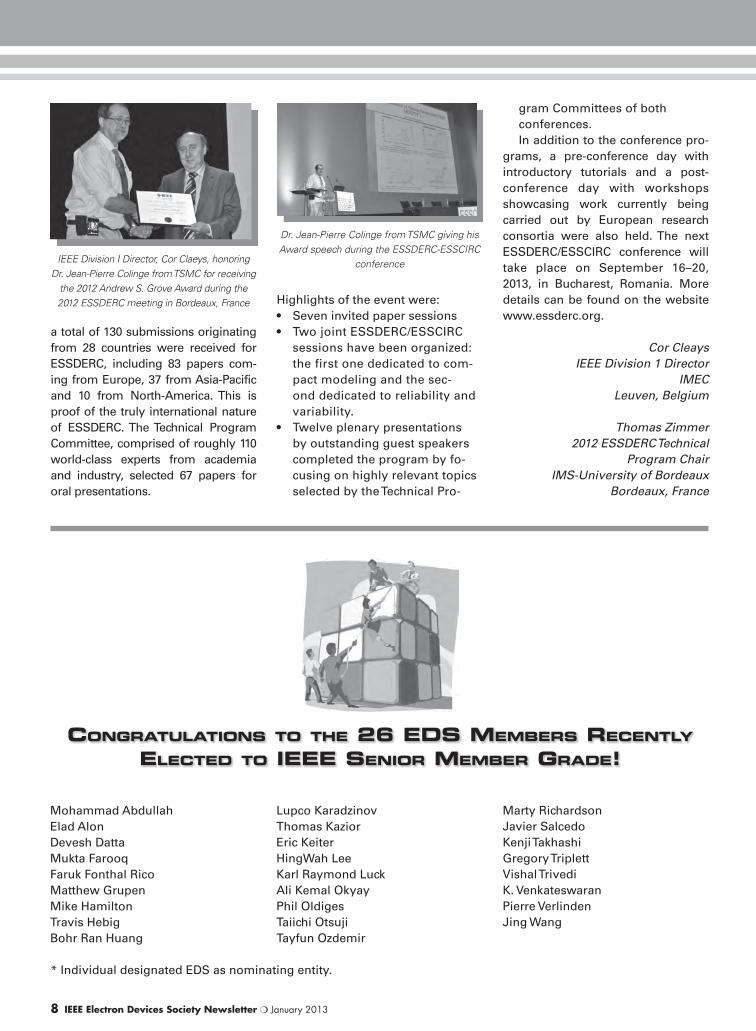
Cor Cleays
IEEE Division 1 Director
IMEC
Leuven, Belgium
Thomas Zimmer
2012 ESSDERC Technical
Program Chair
IMS-University of Bordeaux
Bordeaux, France
Dr. Jean-Pierre Colinge from TSMC giving his Award speech during the ESSDERC-ESSCIRC
conference
Mohammad Abdullah
Elad Alon
Devesh Datta
Mukta Farooq
Faruk Fonthal Rico
Matthew Grupen
Mike Hamilton
Travis Hebig
Bohr Ran Huang
Lupco Karadzinov
Thomas Kazior
Eric Keiter
HingWah Lee
Karl Raymond Luck
Ali Kemal Okyay
Phil Oldiges
Taiichi Otsuji
Tayfun Ozdemir
Marty Richardson
Javier Salcedo
Kenji Takhashi
Gregory Triplett
Vishal Trivedi
K. Venkateswaran
Pierre Verlinden
Jing Wang
* Individual designated EDS as nominating entity.
IEEE Division I Director, Cor Claeys, honoring Dr. Jean-Pierre Colinge from TSMC for receiving
the 2012 Andrew S. Grove Award during the 2012 ESSDERC meeting in Bordeaux, France
January 2013 ❍ IEEE Electron Devices Society Newsletter 9
If you have been in professional
practice for 10 years, you may be eligi-
ble for Senior Membership, the highest
grade of membership for which an indi-
vidual can apply. New senior members
receive a wood and bronze plaque and
a credit certificate for up to US$25 for
a new IEEE society membership. Upon
request a letter will be sent to employ-
ers, recognizing this new status.
For more information on senior
member status, visit: http://www.
ieee.org/web/membership/senior-
members/status.html
To apply for senior member sta-
tus, fill out the on-line application:
http://www.ieee.org/organizations/
rab/md/smelev.html. Please re-
member to designate the Electron
Devices Society as your nominating
entity!
ANNOUNCEMENT OF THE 2012 EDS PH.D. STUDENT FELLOWSHIP WINNERS
The Electron Devices Society Ph.D.
Student Fellowship Program was de-
signed to promote, recognize, and
support Ph.D. level study and research
within the Electron Devices Society’s
field of interest: The field of interest for
EDS is all aspects of engineering, phys-
ics, theory, experiment and simulation
of electron and ion devices involving
insulators, metals, organic materials,
plasmas, semiconductors, quantum-
effect materials, vacuum, and emerg-
ing materials. Specific applications of
these devices include bioelectronics,
biomedical, computation, communi-
cations, displays, electro and micro
mechanics, imaging, micro actuators,
optical, photovoltaics, power, sensors
and signal processing.
The Society is concerned with
research, development, design and
manufacture related to materials,
processing, technology, and appli-
cations of such devices, and scien-
tific, technical, educational and other
activities that contribute to the ad-
vancement of this field.
EDS proudly announces three
EDS Ph.D. Student Fellowship win-
ners for 2012. Brief biographies of
the recipients appear below. De-
tailed articles about each Ph.D. Stu-
dent Fellowship winner and their
work will appear in forthcoming is-
sues of the EDS Newsletter.
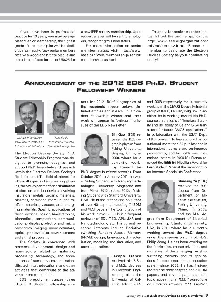
Bin Gao (S’08) re-
ceived the B.S. de-
gree in physics from
Peking University,
Beijing, China, in
2008, where he is
currently work-
ing toward the
Ph.D. degree in microelectronics. From
October 2010 to January 2011, he was
a Visiting Student with Nanyang Tech-
nological University, Singapore and
from March 2012 to June 2012, a Visit-
ing Student with Stanford University,
USA. He is the author and co-author
of over 40 papers, including 7 IEDM
and VLSI papers. The total citation of
his work is over 200. He is a frequent
reviewer of EDL, T-ED, APL, JAP, and
Nanotechnology, etc. His current re-
search interests include Resistive
switching Random Access Memory
(RRAM) design, fabrication, character-
ization, modeling and simulation, and
novel application.
Jacopo Francoreceived his B.Sc.
and M.Sc. degrees
in Electronic Engi-
neering from the
University of Cal-
abria, Italy, in 2005
and 2008 respectively. He is currently
working in the CMOS Device Reliability
group of IMEC, Leuven, Belgium. In ad-
dition, he is working toward his Ph.D.
degree on the topic of “Interface Stabil-
ity and Reliability of Ge and SiGe tran-
sistors for future CMOS applications/”
in collaboration with the ESAT Dept.
of KU Leuven. He has authored or co-
authored more than 50 publications in
international journals and conferences
proceedings, and he holds one inter-
national patent. In 2009 Mr. Franco re-
ceived the IEEE Ed Nicollian Award for
Best Student Paper at the Semiconduc-
tor Interface Specialists Conference.
Shimeng Yu (S’10)
received the B.S.
degree from De-
partment of Mi-
croelectronics,
Peking University,
China, in 2009,
and the M.S. de-
gree from Department of Electrical
Engineering, Stanford University,
USA, in 2011, where he is currently
working toward the Ph.D. degree
under the supervision of Prof. H.-S.
Philip Wong. He has been working on
the fabrication, characterization, and
modelling of the emerging resistive
switching memory and its applica-
tions for neuromorphic computation
system since 2008. He has first-au-
thored one book chapter, and 5 IEDM
papers, and several papers on this
topic appearing in IEEE Transactions
on Electron Devices, IEEE Electron
Meyya MeyyappanEDS Vice-President of Educational Activities
Agis Iliadis EDS PhD & Masters
Student Fellowship Chair
10 IEEE Electron Devices Society Newsletter ❍ January 2013
Device Letters, Applied Physics Let-
ters, Nanotechnology, Phys. Rev.
B, etc. His papers have been cited
more than 200 times in the past
three years with H-index 9.
Shimeng Yu had a summer intern-
ship in IMEC, Belgium, in 2011, and a
summer internship at the IBM TJ Wat-
son Research Center, USA, in 2012.
He was awarded the Stanford Gradu-
ate Fellowship 2009-2012, IEEE Elec-
tron Devices Society Masters Student
Fellowship 2010, and IEEE Electron
Devices Society Ph.D. Student Fel-
lowship 2012.
Meyya Meyyappan
EDS Vice-President of Educational
Activities
NASA Ames Research Center
Moffett Field, CA, USA
Agis Iliadis
EDS Ph.D. & Masters Student
Fellowship Chair
University of Maryland
College Park, MD, USA
CALL FOR NOMINATIONS
2013 IEEE ELECTRON DEVICES SOCIETY
PHD STUDENT FELLOWSHIPDescription: One year fellowships awarded to promote, recognize, and support PhD level study and research
within the Electron Devices Society’s field of interest: The field of interest for EDS is all aspects of engineering,
physics, theory, experiment and simulation of electron and ion devices involving insulators, metals, organic
materials, plasmas, semiconductors, quantum-effect materials, vacuum, and emerging materials. Specific ap-
plications of these devices include bioelectronics, biomedical, computation, communications, displays, electro
and micro mechanics, imaging, micro actuators, optical, photovoltaics, power, sensors and signal processing.
It is expected that three fellowships will be awarded, with the intention of at least one fellowship being given
to eligible students in each of the following geographical regions every year: Americas, Europe/Middle East/
Africa, and Asia & Pacific. Only one candidate can win per educational institution.
Prize: US$5,000 to the student and if necessary funds are also available to assist in covering travel and ac-
commodation costs for each recipient to attend the EDS Administrative Committee meeting for presentation of
the award plaque. The EDS Newsletter will feature articles about the EDS PhD Fellows and their work over the
course of the next year.
Eligibility: Candidate must: be an IEEE EDS student member at the time of nomination; be pursuing a doc-
torate degree within the EDS field of interest on a full-time basis; and continue his/her studies at the current
institution with the same faculty advisor for twelve months after receipt of award. Nominator must be an IEEE
EDS member. Previous award winners are ineligible.
Basis for Judging: Demonstration of his/her significant ability to perform independent research in the fields
of electron devices and a proven history of academic excellence.
Nomination Package:• Nominating letter by an EDS member
• Two-page (maximum) statement by the student describing his or her education and research interests, ac-
complishments and graduation date
• One-page biographical sketch of the student (including student’s mailing address and email address)
• One copy of the student’s under-graduate and graduate transcripts/grades. Please provide an explanation of
the grading system if different from the A-F format.
• Two letters of recommendation from individuals familiar with the student’s research and educational cre-
dentials. Letters of recommendation cannot be from the nominator.
Timetable:• Nomination packages are due at the EDS Executive Office no later than May 15, 2013
• Recipients will be notified by July 15, 2013
• Monetary awards will be given by August 15, 2013
• Formal award presentation will take place at the EDS Administrative Committee Meeting in December 2013.
• A hard copy of all nomination packages must be received by mail at the EDS Office no later than the May 15
deadline in order to be eligible for the award.
Send completed package to: IEEE Operations Center
EDS Executive Office – PhD Student Fellowship Program
445 Hoes Lane, Piscataway, NJ 08854 USA
For more information contact: [email protected]
Visit the EDS website: http://eds.ieee.org/eds-phd-student-fellowship-program.html
January 2013 ❍ IEEE Electron Devices Society Newsletter 11
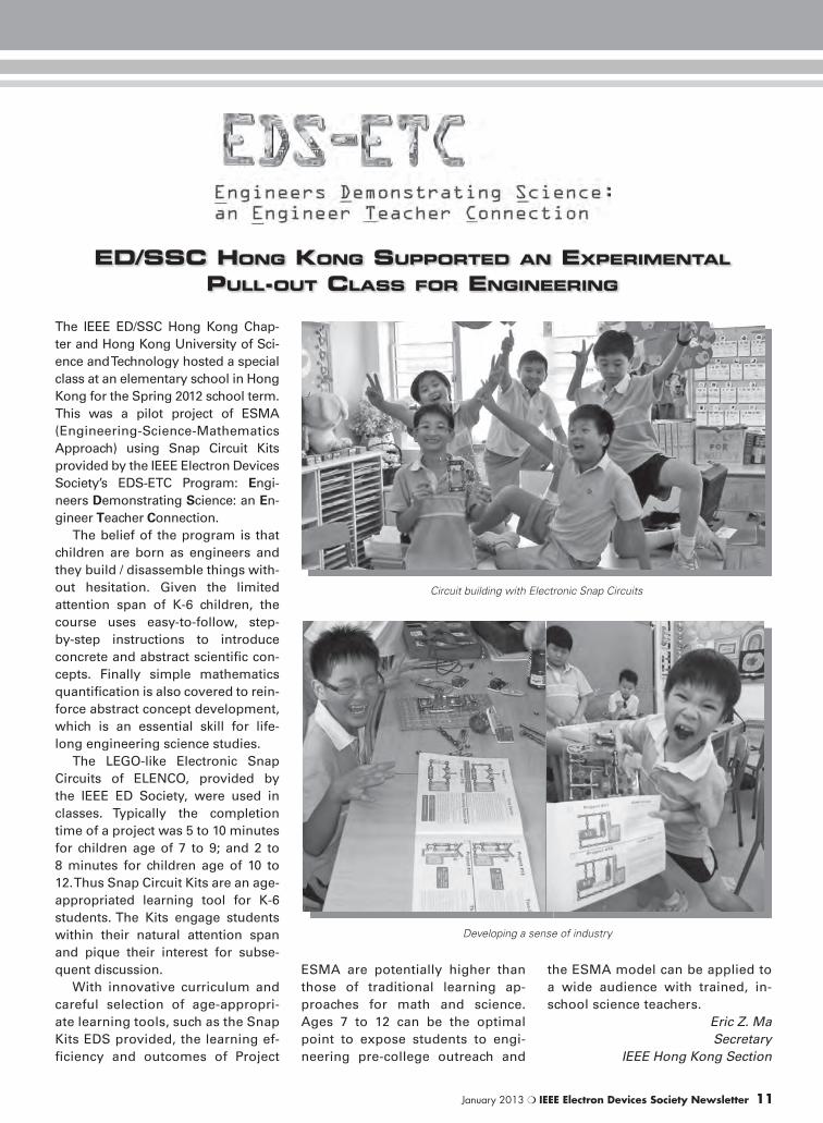
ED/SSC HONG KONG SUPPORTED AN EXPERIMENTAL PULL-OUT CLASS FOR ENGINEERING
The IEEE ED/SSC Hong Kong Chap-
ter and Hong Kong University of Sci-
ence and Technology hosted a special
class at an elementary school in Hong
Kong for the Spring 2012 school term.
This was a pilot project of ESMA
(Engineering-Science-Mathematics
Approach) using Snap Circuit Kits
provided by the IEEE Electron Devices
Society’s EDS-ETC Program: Engi-
neers Demonstrating Science: an En-
gineer Teacher Connection.
The belief of the program is that
children are born as engineers and
they build / disassemble things with-
out hesitation. Given the limited
attention span of K-6 children, the
course uses easy-to-follow, step-
by-step instructions to introduce
concrete and abstract scientific con-
cepts. Finally simple mathematics
quantification is also covered to rein-
force abstract concept development,
which is an essential skill for life-
long engineering science studies.
The LEGO-like Electronic Snap
Circuits of ELENCO, provided by
the IEEE ED Society, were used in
classes. Typically the completion
time of a project was 5 to 10 minutes
for children age of 7 to 9; and 2 to
8 minutes for children age of 10 to
12. Thus Snap Circuit Kits are an age-
appropriated learning tool for K-6
students. The Kits engage students
within their natural attention span
and pique their interest for subse-
quent discussion.
With innovative curriculum and
careful selection of age-appropri-
ate learning tools, such as the Snap
Kits EDS provided, the learning ef-
ficiency and outcomes of Project
ESMA are potentially higher than
those of traditional learning ap-
proaches for math and science.
Ages 7 to 12 can be the optimal
point to expose students to engi-
neering pre-college outreach and
the ESMA model can be applied to
a wide audience with trained, in-
school science teachers.
Eric Z. Ma
Secretary
IEEE Hong Kong Section
Circuit building with Electronic Snap Circuits
Developing a sense of industry
12 IEEE Electron Devices Society Newsletter ❍ January 2013
“DISCOVERING THE NEW ENGINEERING POTENTIAL TALENTS oF oUR TIME”
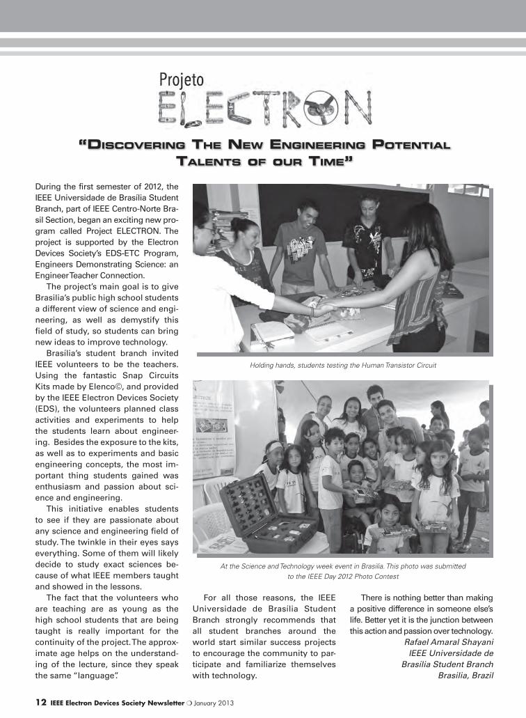
During the first semester of 2012, the
IEEE Universidade de Brasília Student
Branch, part of IEEE Centro-Norte Bra-
sil Section, began an exciting new pro-
gram called Project ELECTRON. The
project is supported by the Electron
Devices Society’s EDS-ETC Program,
Engineers Demonstrating Science: an
Engineer Teacher Connection.
The project’s main goal is to give
Brasilia’s public high school students
a different view of science and engi-
neering, as well as demystify this
field of study, so students can bring
new ideas to improve technology.
Brasília’s student branch invited
IEEE volunteers to be the teachers.
Using the fantastic Snap Circuits
Kits made by Elenco©, and provided
by the IEEE Electron Devices Society
(EDS), the volunteers planned class
activities and experiments to help
the students learn about engineer-
ing. Besides the exposure to the kits,
as well as to experiments and basic
engineering concepts, the most im-
portant thing students gained was
enthusiasm and passion about sci-
ence and engineering.
This initiative enables students
to see if they are passionate about
any science and engineering field of
study. The twinkle in their eyes says
everything. Some of them will likely
decide to study exact sciences be-
cause of what IEEE members taught
and showed in the lessons.
The fact that the volunteers who
are teaching are as young as the
high school students that are being
taught is really important for the
continuity of the project. The approx-
imate age helps on the understand-
ing of the lecture, since they speak
the same “language”.
For all those reasons, the IEEE
Universidade de Brasília Student
Branch strongly recommends that
all student branches around the
world start similar success projects
to encourage the community to par-
ticipate and familiarize themselves
with technology.
There is nothing better than making
a positive difference in someone else’s
life. Better yet it is the junction between
this action and passion over technology.
Rafael Amaral Shayani
IEEE Universidade de
Brasília Student Branch
Brasilia, Brazil
At the Science and Technology week event in Brasilia. This photo was submitted to the IEEE Day 2012 Photo Contest
Holding hands, students testing the Human Transistor Circuit
January 2013 ❍ IEEE Electron Devices Society Newsletter 13
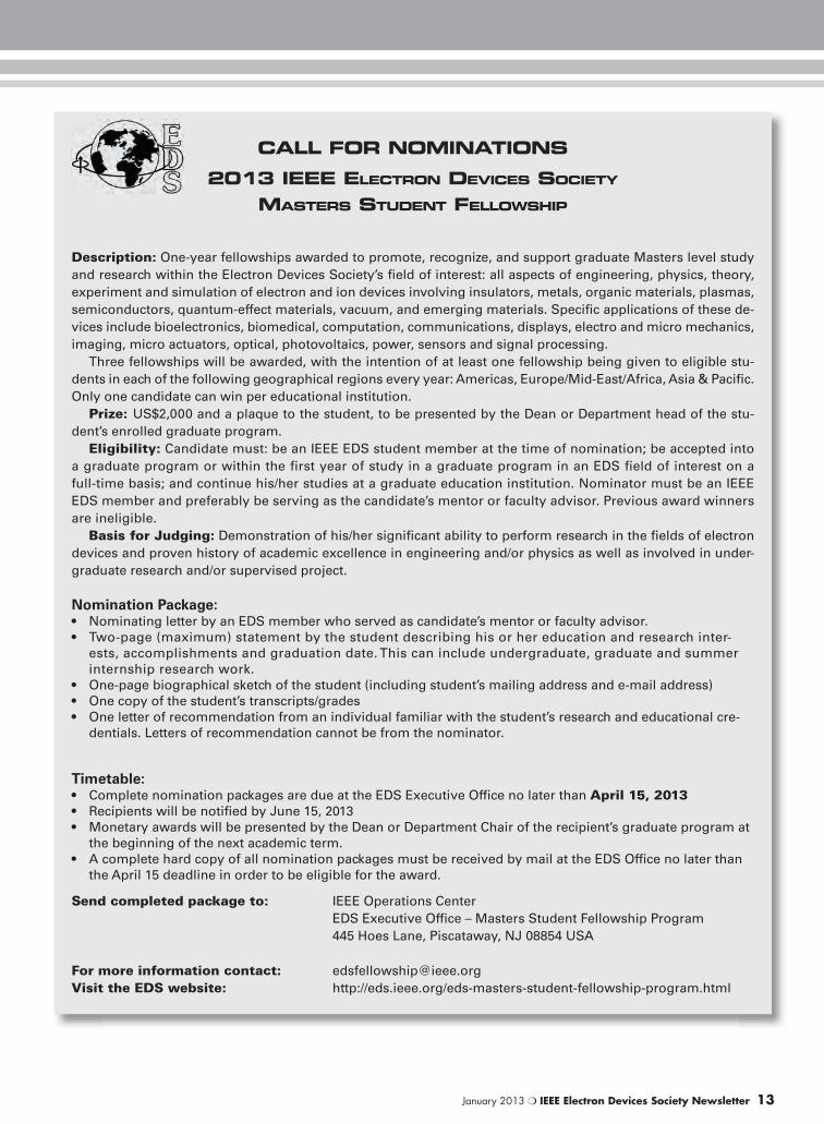
CALL FOR NOMINATIONS
2013 IEEE ELECTRON DEVICES SOCIETY MASTERS STUDENT FELLOWSHIP
Description: One-year fellowships awarded to promote, recognize, and support graduate Masters level study
and research within the Electron Devices Society’s field of interest: all aspects of engineering, physics, theory,
experiment and simulation of electron and ion devices involving insulators, metals, organic materials, plasmas,
semiconductors, quantum-effect materials, vacuum, and emerging materials. Specific applications of these de-
vices include bioelectronics, biomedical, computation, communications, displays, electro and micro mechanics,
imaging, micro actuators, optical, photovoltaics, power, sensors and signal processing.
Three fellowships will be awarded, with the intention of at least one fellowship being given to eligible stu-
dents in each of the following geographical regions every year: Americas, Europe/Mid-East/Africa, Asia & Pacific.
Only one candidate can win per educational institution.
Prize: US$2,000 and a plaque to the student, to be presented by the Dean or Department head of the stu-
dent’s enrolled graduate program.
Eligibility: Candidate must: be an IEEE EDS student member at the time of nomination; be accepted into
a graduate program or within the first year of study in a graduate program in an EDS field of interest on a
full-time basis; and continue his/her studies at a graduate education institution. Nominator must be an IEEE
EDS member and preferably be serving as the candidate’s mentor or faculty advisor. Previous award winners
are ineligible.
Basis for Judging: Demonstration of his/her significant ability to perform research in the fields of electron
devices and proven history of academic excellence in engineering and/or physics as well as involved in under-
graduate research and/or supervised project.
Nomination Package:• Nominating letter by an EDS member who served as candidate’s mentor or faculty advisor.
• Two-page (maximum) statement by the student describing his or her education and research inter-
ests, accomplishments and graduation date. This can include undergraduate, graduate and summer
internship research work.
• One-page biographical sketch of the student (including student’s mailing address and e-mail address)
• One copy of the student’s transcripts/grades
• One letter of recommendation from an individual familiar with the student’s research and educational cre-
dentials. Letters of recommendation cannot be from the nominator.
Timetable:• Complete nomination packages are due at the EDS Executive Office no later than April 15, 2013
• Recipients will be notified by June 15, 2013
• Monetary awards will be presented by the Dean or Department Chair of the recipient’s graduate program at
the beginning of the next academic term.
• A complete hard copy of all nomination packages must be received by mail at the EDS Office no later than
the April 15 deadline in order to be eligible for the award.
Send completed package to: IEEE Operations Center
EDS Executive Office – Masters Student Fellowship Program
445 Hoes Lane, Piscataway, NJ 08854 USA
For more information contact: [email protected]
Visit the EDS website: http://eds.ieee.org/eds-masters-student-fellowship-program.html
14 IEEE Electron Devices Society Newsletter ❍ January 2013
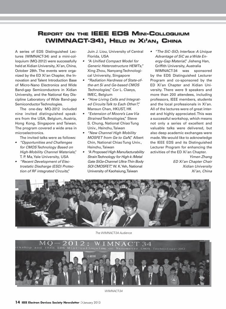
REPORT ON THE IEEE EDS MINI-COLLOQUIUM (WIMNACT-34), HELD IN XI’AN, CHINA
A series of EDS Distinguished Lec-
tures (WIMNACT-34) and a mini-col-
loquium (MQ-2012) were successfully
held at Xidian University, Xi’an, China,
October 28th. The events were orga-
nized by the ED Xi’an Chapter, the In-
novation and Talent Introduction Base
of Micro-Nano Electronics and Wide
Band-gap Semiconductors in Xidian
University, and the National Key Dis-
cipline Laboratory of Wide Band-gap
Semiconductor Technologies.
The one-day MQ-2012 included
nine invited distinguished speak-
ers from the USA, Belgium, Austria,
Hong Kong, Singapore and Taiwan.
The program covered a wide area in
microelectronics.
The invited talks were as follows:
• “Opportunities and Challenges
for CMOS Technology Based on
High-Mobility Channel Materials,”
T. P. Ma, Yale University, USA
• “Recent Development of Elec-
trostatic Discharge (ESD) Protec-
tion of RF integrated Circuits,”
Juin J. Liou, University of Central
Florida, USA
• “A Unified Compact Model for
Generic Heterostructure HEMTs,”
Xing Zhou, Nanyang Technologi-
cal University, Singapore
• “Radiation Hardness of State-of-
the-art Si and Ge-based CMOS
Technologies,” Cor L. Claeys,
IMEC, Belgium
• “How Living Cells and Integrat-
ed Circuits Talk to Each Other?,”
Mansun Chan, HKUST, HK
• “Extension of Moore’s Law Via
Strained Technologies,” Steve
S. Chung, National Chiao Tung
Univ., Hsinchu, Taiwan
• “New Channel High Mobility
MOSFET from Ge to GaN,” Albert
Chin, National Chiao Tung Univ.,
Hsinchu, Taiwan
• “A Proposed High Manufacturability
Strain Technology for High-k /Metal
Gate SiGe-Channel Ultra-Thin Body
SOI CMOSFET,” W. K. Yeh, National
University of Kaohsiung, Taiwan
• “The SiC–SiO2 Interface: A Unique
Advantage of SiC as a Wide En-
ergy-Gap Material,” Jisheng Han,
Griffith University, Australia
WIMNACT-34 was sponsored
by the EDS Distinguished Lecturer
Program and co-sponsored by the
ED Xi’an Chapter and Xidian Uni-
versity. There were 9 speakers and
more than 200 attendees, including
professors, IEEE members, students
and the local professionals in Xi’an.
All of the lectures were of great inter-
est and highly appreciated. This was
a successful workshop, which means
not only a series of excellent and
valuable talks were delivered, but
also deep academic exchanges were
made. We would like to acknowledge
the IEEE EDS and its Distinguished
Lecturer Program for enhancing the
activities of the ED Xi’an Chapter.
Yimen Zhang
ED Xi’an Chapter Chair
Xidian University
Xi’an, China
WIMNACT-34
The WIMNACT-34 Audience
January 2013 ❍ IEEE Electron Devices Society Newsletter 15
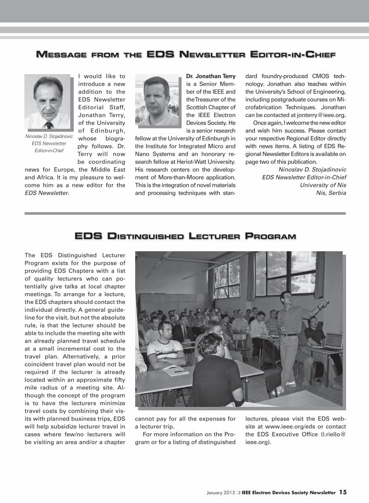
MESSAGE FROM THE EDS NEWSLETTER EDITOR-IN-CHIEF
I would like to
introduce a new
addition to the
EDS Newsletter
Editorial Staff,
Jonathan Terry,
of the University
of Edinburgh,
whose biogra-
phy follows. Dr.
Terry will now
be coordinating
news for Europe, the Middle East
and Africa. It is my pleasure to wel-
come him as a new editor for the
EDS Newsletter.
Dr. Jonathan Terryis a Senior Mem-
ber of the IEEE and
the Treasurer of the
Scottish Chapter of
the IEEE Electron
Devices Society. He
is a senior research
fellow at the University of Edinburgh in
the Institute for Integrated Micro and
Nano Systems and an honorary re-
search fellow at Heriot-Watt University.
His research centers on the develop-
ment of More-than-Moore application.
This is the integration of novel materials
and processing techniques with stan-
dard foundry-produced CMOS tech-
nology. Jonathan also teaches within
the University’s School of Engineering,
including postgraduate courses on Mi-
crofabrication Techniques. Jonathan
can be contacted at [email protected].
Once again, I welcome the new editor
and wish him success. Please contact
your respective Regional Editor directly
with news items. A listing of EDS Re-
gional Newsletter Editors is available on
page two of this publication.
Ninoslav D. Stojadinovic
EDS Newsletter Editor-in-Chief
University of Nis
Nis, Serbia
Ninoslav D. Stojadinovic EDS Newsletter
Editor-in-Chief
The EDS Distinguished Lecturer
Program exists for the purpose of
providing EDS Chapters with a list
of quality lecturers who can po-
tentially give talks at local chapter
meetings. To arrange for a lecture,
the EDS chapters should contact the
individual directly. A general guide-
line for the visit, but not the absolute
rule, is that the lecturer should be
able to include the meeting site with
an already planned travel schedule
at a small incremental cost to the
travel plan. Alternatively, a prior
coincident travel plan would not be
required if the lecturer is already
located within an approximate fifty
mile radius of a meeting site. Al-
though the concept of the program
is to have the lecturers minimize
travel costs by combining their vis-
its with planned business trips, EDS
will help subsidize lecturer travel in
cases where few/no lecturers will
be visiting an area and/or a chapter
cannot pay for all the expenses for
a lecturer trip.
For more information on the Pro-
gram or for a listing of distinguished
lectures, please visit the EDS web-
site at www.ieee.org/eds or contact
the EDS Executive Office (l.riello@
ieee.org).
EDS DISTINGUISHED LECTURER PROGRAM
16 IEEE Electron Devices Society Newsletter ❍ January 2013
Interested in know-
ing why it’s not
possible to mea-
sure the built-in
voltage of a PN
junction using a
voltmeter? Do you
need to under-
stand the best way
to derive an ex-
pression for the av-
erage thermal velocity of an electron?
Or are you curious about what quan-
tum dots and wires are? The answers
to these questions and more are avail-
able through the QuestEDS Question
and Answer page.
To ask a question not already
addressed on the Q&A page, visit
www.ieee.org/go/questeds. Techni-
cal experts answering the questions
posed represent academic, govern-
ment, and industry sectors.
Questions are grouped into nine
technical categories and two general
ones. Technical categories cover sub-
ject areas like semiconductor and
device physics, process technology,
device characterization, technology
CAD, compact modeling, VLSI inter-
connects, photovoltaics, and quan-
tum electronics. Subject areas ad-
dressed are anticipated to expand in
the future. Two other categories ad-
dress questions pertaining to educa-
tional activities and general inquiries
about society membership. Within
a two week time frame from when
the question is asked, an answer is
posted online. Incoming questions
are handled by an editor-in-chief
who ensures that they fall within the
technical scope of EDS and that they
are adequately answered.
For the answer to this recent sub-
mission, visit http://eds.ieee.org/mem-
ber-sign-in-form.html?notauth=1.
Your IEEE login is required to view
the answer page. After authentication
you will be redirected to the answer
page, where you can select the appro-
priate topic link.
Samar Saha
EDS Vice-President of Publications
SuVolta, Inc.
Los Gatos, CA, USA
QUESTEDS
Device Physics
Question 057-12
“In a MOSFET at equilibrium (all the 4 terminals are open circuited) charge
transfer takes place either from the metal to the semiconductor (SC) or
from the SC to metal due to a nonzero contact potential between the metal
and SC. But the material between the metal and SC is an insulator. My
question is how such charge transfer takes through an insulator?
Samar Saha EDS Vice-President
of Publications
MEMBERS MAKING NEWS
President Barack Obama Awards EDS Members The National Medal of Technology and InnovationIt is with great pleasure that EDS recognizes Jayant Baliga, Rakesh Agrawal, and Michael F. Tompsett for receiv-
ing the National Medal of Technology and Innovation. As the United States’ highest award for technology in-
novation, this is indeed a great honor and no small tribute to their outstanding careers. EDS congratulates Jay,
Rakesh, and Michael for their achievements. It is an honor to count them among the society’s membership.
EDS members make enormous contributions to not only our field, but to the world at large. We take particular
pride when our colleagues are recognized in an extraordinary manner, such as these recent awards given by
President Obama. The National Medal of Technology and Innovation recipients join other illustrious EDS mem-
bers who have made vital contributions such as Nobel Laureates Charles K. Kao, Willard S. Boyle, George Smith
and Herb Kroemer.
Those of us in EDS can take pride in the accomplishments of members like these and draw inspiration from their
work to continue, in the words of EDS’s vision statement, promoting excellence in the field of electron devices
for the benefit of humanity.
Congratulations, gentlemen. You make EDS proud.
January 2013 ❍ IEEE Electron Devices Society Newsletter 17
R E G I O N A L A N D C H A P T E R N E W S
ED Mid-Hudson Valley–by Fernando Guarin
On Wednesday June 27th, the ED
Mid-Hudson Valley Chapter hosted Dr.
Alberto Valdes-Garcia, who shared in-
sights from his present research work
on silicon-integrated millimeter-wave
communication systems and carbon
electronics. During his “Development
of Graphene-Based RF Integrated Cir-
cuits” talk, he explained how the po-
tential of any new material to make
a significant impact into the modern
world of microelectronics is contin-
gent on its ability to achieve scalable
integration into practical circuits. Dr.
Valdes-Garcia indicated that after
the successful demonstration of gra-
phene devices with cut-off frequen-
cies in the GHz-range, the next major
step to move graphene technology
forward into the practical domain of
RF electronics will be to address the
challenges associated with circuit
integration. His presentation sum-
marized the recent development and
characterization of graphene-based
integrated circuits. Detailing how the
first wafer-scale process developed
for graphene RFIC integration on SiC
wafers was introduced along with the
design and measurements of a 5-GHz
down-conversion mixer. Next, a fre-
quency doubler fabricated on CVD
graphene was presented as a proof-
of-concept of graphene-based circuits
in a 200 mm platform. Finally, some
of the special properties if these ICs
(such as their low sensitivity to tem-
perature variations), and the remain-
ing challenges for graphene RFIC
technology were discussed.
~ Fernando Guarin, Editor
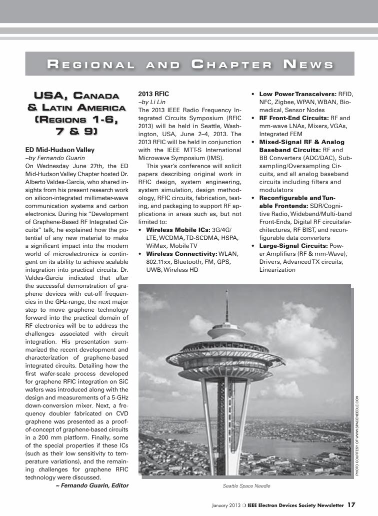
2013 RFIC–by Li Lin
The 2013 IEEE Radio Frequency In-
tegrated Circuits Symposium (RFIC
2013) will be held in Seattle, Wash-
ington, USA, June 2–4, 2013. The
2013 RFIC will be held in conjunction
with the IEEE MTT-S International
Microwave Symposium (IMS).
This year’s conference will solicit
papers describing original work in
RFIC design, system engineering,
system simulation, design method-
ology, RFIC circuits, fabrication, test-
ing, and packaging to support RF ap-
plications in areas such as, but not
limited to:
• Wireless Mobile ICs: 3G/4G/
LTE, WCDMA, TD-SCDMA, HSPA,
WiMax, Mobile TV
• Wireless Connectivity: WLAN,
802.11xx, Bluetooth, FM, GPS,
UWB, Wireless HD
• Low Power Transceivers: RFID,
NFC, Zigbee, WPAN, WBAN, Bio-
medical, Sensor Nodes
• RF Front-End Circuits: RF and
mm-wave LNAs, Mixers, VGAs,
Integrated FEM
• Mixed-Signal RF & Analog
Baseband Circuits: RF and
BB Converters (ADC/DAC), Sub-
sampling/Oversampling Cir-
cuits, and all analog baseband
circuits including filters and
modulators
• Reconfigurable and Tun-
able Frontends: SDR/Cogni-
tive Radio, Wideband/Multi-band
Front-Ends, Digital RF circuits/ar-
chitectures, RF BIST, and recon-
figurable data converters
• Large-Signal Circuits: Pow-
er Amplifiers (RF & mm-Wave),
Drivers, Advanced TX circuits,
Linearization
USA, CANADA & LATIN AMERICA (REGIONS 1-6,
7 & 9)
Seattle Space Needle
PH
OTO
CO
UR
TE
SY
OF
WW
W.S
PAC
EN
EE
DLE
.CO
M
18 IEEE Electron Devices Society Newsletter ❍ January 2013
• VCOs and Frequency Multipli-
ers: RF and mm-Wave VCOs, Fre-
quency Multipliers
• Frequency Generation Circuits:
PLLs, Synthesizers, ADPLL, DDS,
Frequency Dividers
• Modeling and CAD: Active/Pas-
sive Devices, Packaging, EM Sim-
ulation, Co-Simulation
• Device Technologies: CMOS,
SOI, SiGe, GaAs, MEMS, Reliabil-
ity, Characterization, Testing
• mm-Wave SOCs: mm-wave
SOC and SIP systems above
20 GHz for data, video, and imag-
ing apps
• High-Speed Data Transceiv-
ers: Wireline, Wireless, Optical
Transceivers, CDRs for High-
Speed Data links
More information can be found
on the conference website at, http://
www.rfic2013.org.
ED Santa Clara Valley–by Toshishige Yamada
In August, the chapter invited Dr.
K. Ahmed, to give a talk on “Na-
noscale CMOS Contacts: Science
and Technology.” Switching speed in
advanced CMOS transistors has be-
come limited by the increasing para-
sitic resistance, which is dominated
by the always shrinking source/drain
contact area (< 50 nm). The solu-
tion is to reduce contact resistivity.
Dr. Ahmed discussed specific con-
tact resistivity targets and how to
achieve these aggressive targets
using new contact architectures and
equipment platforms. He also raised
the challenges for the new channel
materials.
On October 25th, we co-spon-
sored the Fourth Annual IEEE-SCV
Soft Error Rate (SER) Workshop with
other IEEE chapters. Dr. P. Su of Cis-
co was the Chair of the Workshop
which provided a unique forum for
component manufacturers, assem-
bly houses, and electronic system
manufacturers to exchange innova-
tive ideas and recent results on the
measurement, monitoring, and con-
trol of alpha emission from packag-
ing materials and manufacturing
processes.
In October and November, we
welcomed Dr. R. Rogenmoser, Su-
Volta, “Device Consideration for Low
Power VLSI circuits” and Dr. A. Ber-
gemont, Maxim, “Analog and Mixed-
Signal Technologies,” respectively.
All of our EDS seminars were held at
TI auditorium, Santa Clara, with their
courtesy.
For further information on our
chapter, please visit http://www.ewh.
ieee.org/r6/scv/eds/index.html.
~ Adam Conway, Editor
2012 SBMicro–by João Antonio Martino, Gilson
Wirth, Henri Boudinov, Fred Cioldin
and Jacobus W. Swart
The 27th Symposium on Microelec-
tronics Technology and Devices, SB-
Micro 2012, took place from August
30 to September 2, 2012, in Brasília,
Brazil. It was organized by two Brazil-
ian scientific societies: SBMicro (So-
ciedade Brasileira de Microeletrônica)
and SBC (Sociedade Brasileira de
Computação) and was technically
co-sponsored by the Electrochemical
Society and the IEEE Electron Devices
Society. The SBMicro symposium is a
forum held annually in Brazil dedi-
cated to fabrication and modeling
of microsystems, integrated circuits
and devices. The goal of the sympo-
sium is to bring together researchers
in the fields of processing, materials,
characterization, modeling and TCAD
of integrated circuits, optoelectron-
ics and MEMS. An additional sym-
posium was held at the same place
and time in conjunction with SBMicro
2012: the 25th Symposium on Inte-
grated Circuits and Systems Design.
It was also organized by the same
two local societies. Both symposia
are being held together since 2000,
with a total attendance of more than
300 participants. Local EDS chapters
sponsored a registration fee-free tu-
torial session which was held dur-
ing the first day of the conference.
This full day tutorial session included
three lectures by EDS Distinguished
Lecturers: “Contact Technology
Schemes for Advanced Ge and III-V
CMOS Technologies,” by Cor Claeys
from IMEC, Belgium; “Nanotechnol-
ogy in Electronics and Optoelectron-
ics,” by Meyya Meyyappan, from
NASA, USA; and “Compact Variabil-
ity Modeling for Nanoscale MOS-
FET Devices,” by Samar Saha, from
the University of Colorado, USA.
Additionally, two EDS Distinguished
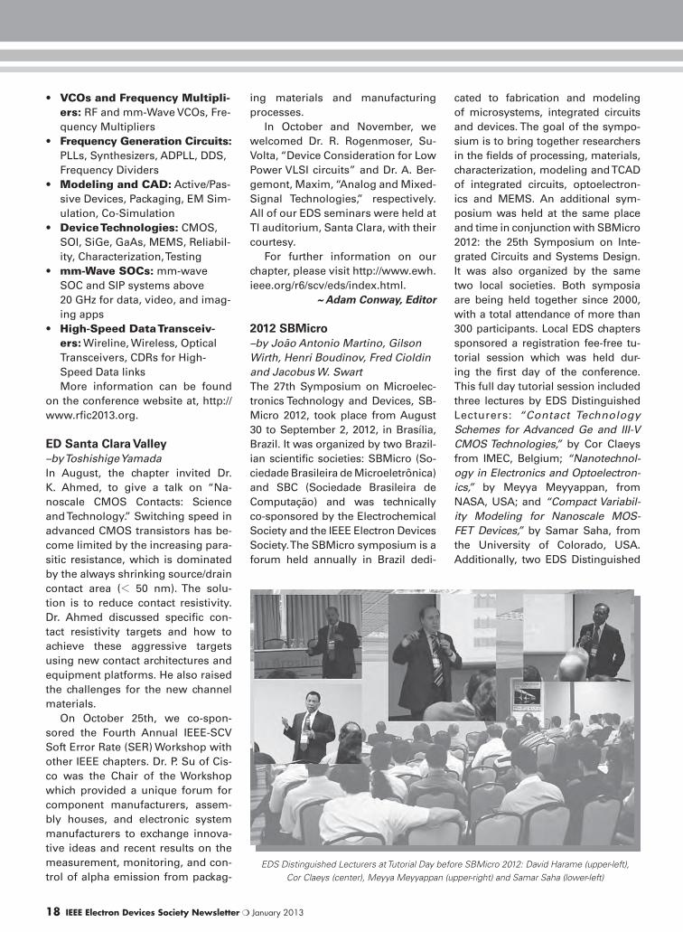
EDS Distinguished Lecturers at Tutorial Day before SBMicro 2012: David Harame (upper-left), Cor Claeys (center), Meyya Meyyappan (upper-right) and Samar Saha (lower-left)
January 2013 ❍ IEEE Electron Devices Society Newsletter 19
Lecturers presented invited talks as
part of the SBMicro 2012 program:
“Nanoenabled Sensors for Security,
Biomedical And Industrial Applica-
tions,” by Meyya Meyyappan and
“History and Future Directions in
SiGe BiCMOS Technology and Its Ap-
plications,” by David Harame, from
IBM, USA.
Following his participation at
SBMicro 2012, IEEE Fellow David
Harame, visited the EDS Student
Chapter at University of Campi-
nas (UNICAMP), in Campinas, and
the ED South Brazil Chapter, in São
Paulo, where he delivered an addi-
tional Distinguished Lecture entitled,
“Advances in Silicon Technology for
Wireless.” The lecture was presented
to a large student and faculty audi-
ence at the Faculty of Electrical and
Computer Engineering of UNICAMP,
and at the Polytechnic School of the
University of Sao Paulo (USP). Dr.
Harame took the opportunity to visit
the Clean Room Labs and discuss
ongoing microelectronics research
at UNICAMP and USP.
The 2012 SBMicro Best Paper
Award was conferred to Felipe Neves
Souza and Renan Trevisoli Doria,
both Ph.D. students at USP. The win-
ning papers were: 1) “Temperature
Influence on Nanowire Tunnel Field
Effect Transistors,” by F. Neves, M. D.
V. Martino, P. G. D. Agopian, J. A. Mar-
tino, R. Rooyackers, D. Leonelli and C.
Claeys, and 2) “Accounting for Short
Channel Effects in the Drain Current
Modeling of Junctionless Nanowire
Transistors,” by R. Trevisoli, R. Doria,
M. de Souza and M. Pavanello.
The 28th Symposium on Micro-
electronics Technology and Devices,
SBMicro 2013, will take place in Cu-
ritiba, Paraná, in the south of Brazil,
from September 3–6, 2013. Topics of
interest include, but are not limited
to: semiconductor processing, IC, op-
toelectronics and MEMS fabrication;
novel materials and devices; reliabil-
ity; technology CAD; displays; ther-
mal effects and models; nanoelec-
tronics; device characterization and
modeling; microsystem networks,
sensors and actuators; package and
technology roadmaps; packaging;
photovoltaic technology, plasma
technology and engineering educa-
tion. Important deadlines are: Sub-
mission: March 31, 2013; Notification
of Acceptance: May 18, 2013; Cam-
era-ready: June 1, 2013. For more in-
formation go to http://www.sbmicro.
org.br/sbmicro and/or contact the
program co-chairs: Jacobus Swart
([email protected]) and Fernando
Guarin ([email protected]).
~ Francisco J. Garcia Sanchez, Editor
New Chapter of the IEEE Electron Devices Society – ED Scotland–by Jonathan Terry
A new chapter representing the
EDS members of Scotland has been
formed. At the inaugural meeting,
Professor David Cumming of the
University of Glasgow was elected
as Chapter Chairman. Other officers
elected were Dr. Jonathan Terry of
the University of Edinburgh as Trea-
surer and Dr. Bhaskar Choubey of the
University of Glasgow as Secretary
and Events Organizer.
A range of events and activities,
including a Mini-Colloquium on Mi-
crosystems, are being planned for
the Chapter’s first year and details
will be circulated in due course.
Further information on the Chap-
ter will shortly be made available
at http://sites.ieee.org/ukri-eds/.
~ Jonathan Terry, Editor
2012 ISPS–by Jan Vobecky
For twenty years, the International
Seminar on Power Semiconductors
EUROPE, MIDDLE EAST & AFRICA
(REGION 8)
Prof. David CummingED Scotland Chapter Chair
The ISPS´12 seminar was held in Prague, Czech Republic
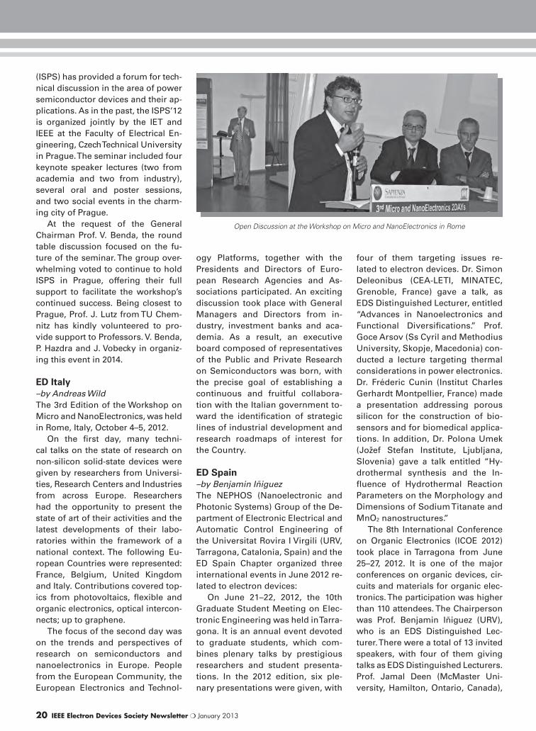
20 IEEE Electron Devices Society Newsletter ❍ January 2013
(ISPS) has provided a forum for tech-
nical discussion in the area of power
semiconductor devices and their ap-
plications. As in the past, the ISPS’12
is organized jointly by the IET and
IEEE at the Faculty of Electrical En-
gineering, Czech Technical University
in Prague. The seminar included four
keynote speaker lectures (two from
academia and two from industry),
several oral and poster sessions,
and two social events in the charm-
ing city of Prague.
At the request of the General
Chairman Prof. V. Benda, the round
table discussion focused on the fu-
ture of the seminar. The group over-
whelming voted to continue to hold
ISPS in Prague, offering their full
support to facilitate the workshop’s
continued success. Being closest to
Prague, Prof. J. Lutz from TU Chem-
nitz has kindly volunteered to pro-
vide support to Professors. V. Benda,
P. Hazdra and J. Vobecky in organiz-
ing this event in 2014.
ED Italy–by Andreas Wild
The 3rd Edition of the Workshop on
Micro and NanoElectronics, was held
in Rome, Italy, October 4–5, 2012.
On the first day, many techni-
cal talks on the state of research on
non-silicon solid-state devices were
given by researchers from Universi-
ties, Research Centers and Industries
from across Europe. Researchers
had the opportunity to present the
state of art of their activities and the
latest developments of their labo-
ratories within the framework of a
national context. The following Eu-
ropean Countries were represented:
France, Belgium, United Kingdom
and Italy. Contributions covered top-
ics from photovoltaics, flexible and
organic electronics, optical intercon-
nects; up to graphene.
The focus of the second day was
on the trends and perspectives of
research on semiconductors and
nanoelectronics in Europe. People
from the European Community, the
European Electronics and Technol-
ogy Platforms, together with the
Presidents and Directors of Euro-
pean Research Agencies and As-
sociations participated. An exciting
discussion took place with General
Managers and Directors from in-
dustry, investment banks and aca-
demia. As a result, an executive
board composed of representatives
of the Public and Private Research
on Semiconductors was born, with
the precise goal of establishing a
continuous and fruitful collabora-
tion with the Italian government to-
ward the identification of strategic
lines of industrial development and
research roadmaps of interest for
the Country.
ED Spain–by Benjamin Iñiguez
The NEPHOS (Nanoelectronic and
Photonic Systems) Group of the De-
partment of Electronic Electrical and
Automatic Control Engineering of
the Universitat Rovira I Virgili (URV,
Tarragona, Catalonia, Spain) and the
ED Spain Chapter organized three
international events in June 2012 re-
lated to electron devices:
On June 21–22, 2012, the 10th
Graduate Student Meeting on Elec-
tronic Engineering was held in Tarra-
gona. It is an annual event devoted
to graduate students, which com-
bines plenary talks by prestigious
researchers and student presenta-
tions. In the 2012 edition, six ple-
nary presentations were given, with
four of them targeting issues re-
lated to electron devices. Dr. Simon
Deleonibus (CEA-LETI, MINATEC,
Grenoble, France) gave a talk, as
EDS Distinguished Lecturer, entitled
“Advances in Nanoelectronics and
Functional Diversifications.” Prof.
Goce Arsov (Ss Cyril and Methodius
University, Skopje, Macedonia) con-
ducted a lecture targeting thermal
considerations in power electronics.
Dr. Fréderic Cunin (Institut Charles
Gerhardt Montpellier, France) made
a presentation addressing porous
silicon for the construction of bio-
sensors and for biomedical applica-
tions. In addition, Dr. Polona Umek
(Jožef Stefan Institute, Ljubljana,
Slovenia) gave a talk entitled “Hy-
drothermal synthesis and the In-
fluence of Hydrothermal Reaction
Parameters on the Morphology and
Dimensions of Sodium Titanate and
MnO2 nanostructures.”
The 8th International Conference
on Organic Electronics (ICOE 2012)
took place in Tarragona from June
25–27, 2012. It is one of the major
conferences on organic devices, cir-
cuits and materials for organic elec-
tronics. The participation was higher
than 110 attendees. The Chairperson
was Prof. Benjamin Iñiguez (URV),
who is an EDS Distinguished Lec-
turer. There were a total of 13 invited
speakers, with four of them giving
talks as EDS Distinguished Lecturers.
Prof. Jamal Deen (McMaster Uni-
versity, Hamilton, Ontario, Canada),
Open Discussion at the Workshop on Micro and NanoElectronics in Rome
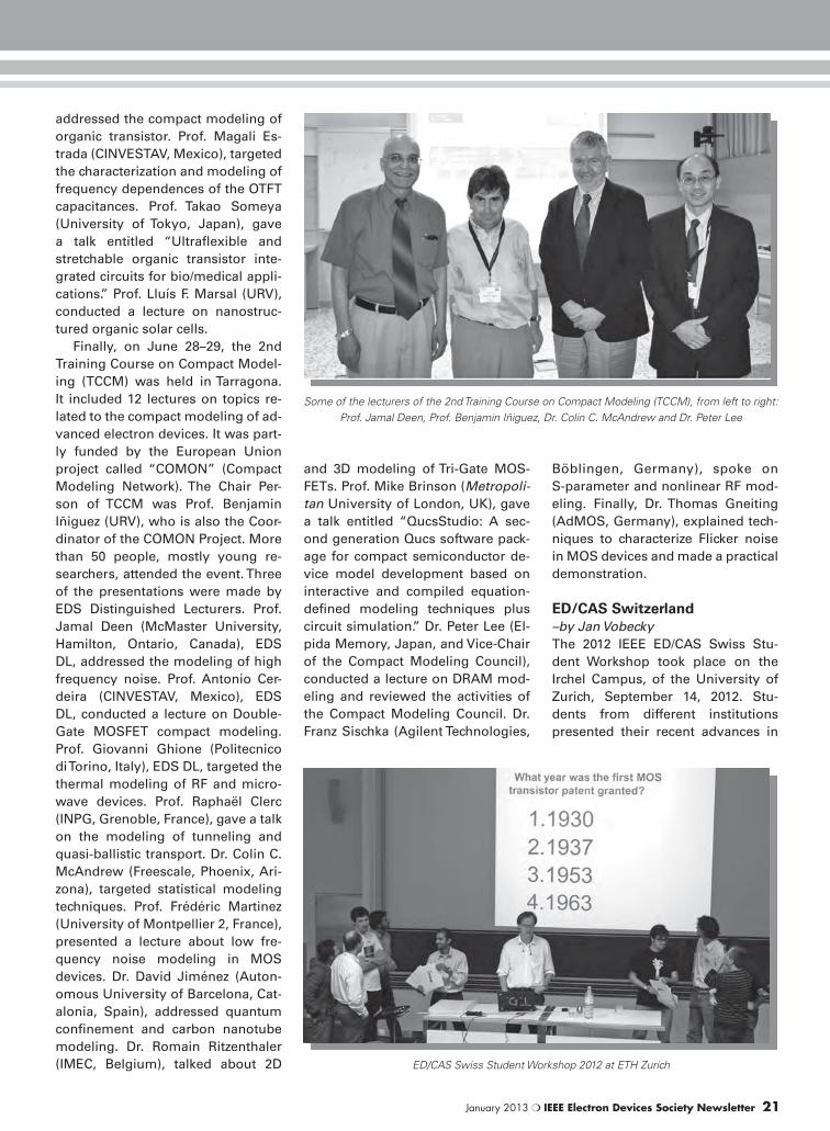
January 2013 ❍ IEEE Electron Devices Society Newsletter 21
addressed the compact modeling of
organic transistor. Prof. Magali Es-
trada (CINVESTAV, Mexico), targeted
the characterization and modeling of
frequency dependences of the OTFT
capacitances. Prof. Takao Someya
(University of Tokyo, Japan), gave
a talk entitled “Ultraflexible and
stretchable organic transistor inte-
grated circuits for bio/medical appli-
cations.” Prof. Lluís F. Marsal (URV),
conducted a lecture on nanostruc-
tured organic solar cells.
Finally, on June 28–29, the 2nd
Training Course on Compact Model-
ing (TCCM) was held in Tarragona.
It included 12 lectures on topics re-
lated to the compact modeling of ad-
vanced electron devices. It was part-
ly funded by the European Union
project called “COMON” (Compact
Modeling Network). The Chair Per-
son of TCCM was Prof. Benjamin
Iñiguez (URV), who is also the Coor-
dinator of the COMON Project. More
than 50 people, mostly young re-
searchers, attended the event. Three
of the presentations were made by
EDS Distinguished Lecturers. Prof.
Jamal Deen (McMaster University,
Hamilton, Ontario, Canada), EDS
DL, addressed the modeling of high
frequency noise. Prof. Antonio Cer-
deira (CINVESTAV, Mexico), EDS
DL, conducted a lecture on Double-
Gate MOSFET compact modeling.
Prof. Giovanni Ghione (Politecnico
di Torino, Italy), EDS DL, targeted the
thermal modeling of RF and micro-
wave devices. Prof. Raphaël Clerc
(INPG, Grenoble, France), gave a talk
on the modeling of tunneling and
quasi-ballistic transport. Dr. Colin C.
McAndrew (Freescale, Phoenix, Ari-
zona), targeted statistical modeling
techniques. Prof. Frédéric Martinez
(University of Montpellier 2, France),
presented a lecture about low fre-
quency noise modeling in MOS
devices. Dr. David Jiménez (Auton-
omous University of Barcelona, Cat-
alonia, Spain), addressed quantum
confinement and carbon nanotube
modeling. Dr. Romain Ritzenthaler
(IMEC, Belgium), talked about 2D
and 3D modeling of Tri-Gate MOS-
FETs. Prof. Mike Brinson (Metropoli-
tan University of London, UK), gave
a talk entitled “QucsStudio: A sec-
ond generation Qucs software pack-
age for compact semiconductor de-
vice model development based on
interactive and compiled equation-
defined modeling techniques plus
circuit simulation.” Dr. Peter Lee (El-
pida Memory, Japan, and Vice-Chair
of the Compact Modeling Council),
conducted a lecture on DRAM mod-
eling and reviewed the activities of
the Compact Modeling Council. Dr.
Franz Sischka (Agilent Technologies,
Böblingen, Germany), spoke on
S-parameter and nonlinear RF mod-
eling. Finally, Dr. Thomas Gneiting
(AdMOS, Germany), explained tech-
niques to characterize Flicker noise
in MOS devices and made a practical
demonstration.
ED/CAS Switzerland–by Jan Vobecky
The 2012 IEEE ED/CAS Swiss Stu-
dent Workshop took place on the
Irchel Campus, of the University of
Zurich, September 14, 2012. Stu-
dents from different institutions
presented their recent advances in
Some of the lecturers of the 2nd Training Course on Compact Modeling (TCCM), from left to right: Prof. Jamal Deen, Prof. Benjamin Iñiguez, Dr. Colin C. McAndrew and Dr. Peter Lee
ED/CAS Swiss Student Workshop 2012 at ETH Zurich
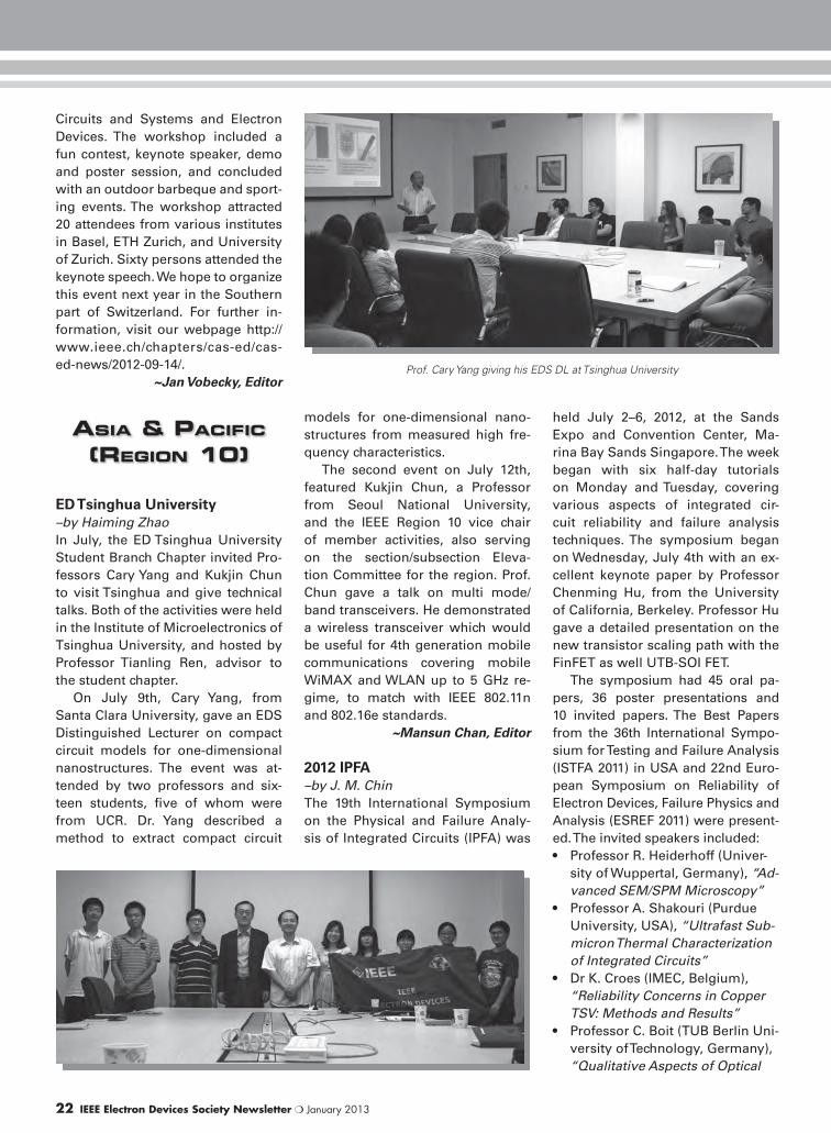
22 IEEE Electron Devices Society Newsletter ❍ January 2013
Circuits and Systems and Electron
Devices. The workshop included a
fun contest, keynote speaker, demo
and poster session, and concluded
with an outdoor barbeque and sport-
ing events. The workshop attracted
20 attendees from various institutes
in Basel, ETH Zurich, and University
of Zurich. Sixty persons attended the
keynote speech. We hope to organize
this event next year in the Southern
part of Switzerland. For further in-
formation, visit our webpage http://
www.ieee.ch/chapters/cas-ed/cas-
ed-news/2012-09-14/.
~Jan Vobecky, Editor
ED Tsinghua University –by Haiming Zhao
In July, the ED Tsinghua University
Student Branch Chapter invited Pro-
fessors Cary Yang and Kukjin Chun
to visit Tsinghua and give technical
talks. Both of the activities were held
in the Institute of Microelectronics of
Tsinghua University, and hosted by
Professor Tianling Ren, advisor to
the student chapter.
On July 9th, Cary Yang, from
Santa Clara University, gave an EDS
Distinguished Lecturer on compact
circuit models for one-dimensional
nanostructures. The event was at-
tended by two professors and six-
teen students, five of whom were
from UCR. Dr. Yang described a
method to extract compact circuit
models for one-dimensional nano-
structures from measured high fre-
quency characteristics.
The second event on July 12th,
featured Kukjin Chun, a Professor
from Seoul National University,
and the IEEE Region 10 vice chair
of member activities, also serving
on the section/subsection Eleva-
tion Committee for the region. Prof.
Chun gave a talk on multi mode/
band transceivers. He demonstrated
a wireless transceiver which would
be useful for 4th generation mobile
communications covering mobile
WiMAX and WLAN up to 5 GHz re-
gime, to match with IEEE 802.11n
and 802.16e standards.
~ Mansun Chan, Editor
2012 IPFA–by J. M. Chin
The 19th International Symposium
on the Physical and Failure Analy-
sis of Integrated Circuits (IPFA) was
held July 2–6, 2012, at the Sands
Expo and Convention Center, Ma-
rina Bay Sands Singapore. The week
began with six half-day tutorials
on Monday and Tuesday, covering
various aspects of integrated cir-
cuit reliability and failure analysis
techniques. The symposium began
on Wednesday, July 4th with an ex-
cellent keynote paper by Professor
Chenming Hu, from the University
of California, Berkeley. Professor Hu
gave a detailed presentation on the
new transistor scaling path with the
FinFET as well UTB-SOI FET.
The symposium had 45 oral pa-
pers, 36 poster presentations and
10 invited papers. The Best Papers
from the 36th International Sympo-
sium for Testing and Failure Analysis
(ISTFA 2011) in USA and 22nd Euro-
pean Symposium on Reliability of
Electron Devices, Failure Physics and
Analysis (ESREF 2011) were present-
ed. The invited speakers included:
• Professor R. Heiderhoff (Univer-
sity of Wuppertal, Germany), “Ad-
vanced SEM/SPM Microscopy”
• Professor A. Shakouri (Purdue
University, USA), “Ultrafast Sub-
micron Thermal Characterization
of Integrated Circuits”
• Dr K. Croes (IMEC, Belgium),
“Reliability Concerns in Copper
TSV: Methods and Results”
• Professor C. Boit (TUB Berlin Uni-
versity of Technology, Germany),
“Qualitative Aspects of Optical
ASIA & PACIFIC (REGION 10)
Prof. Cary Yang giving his EDS DL at Tsinghua University
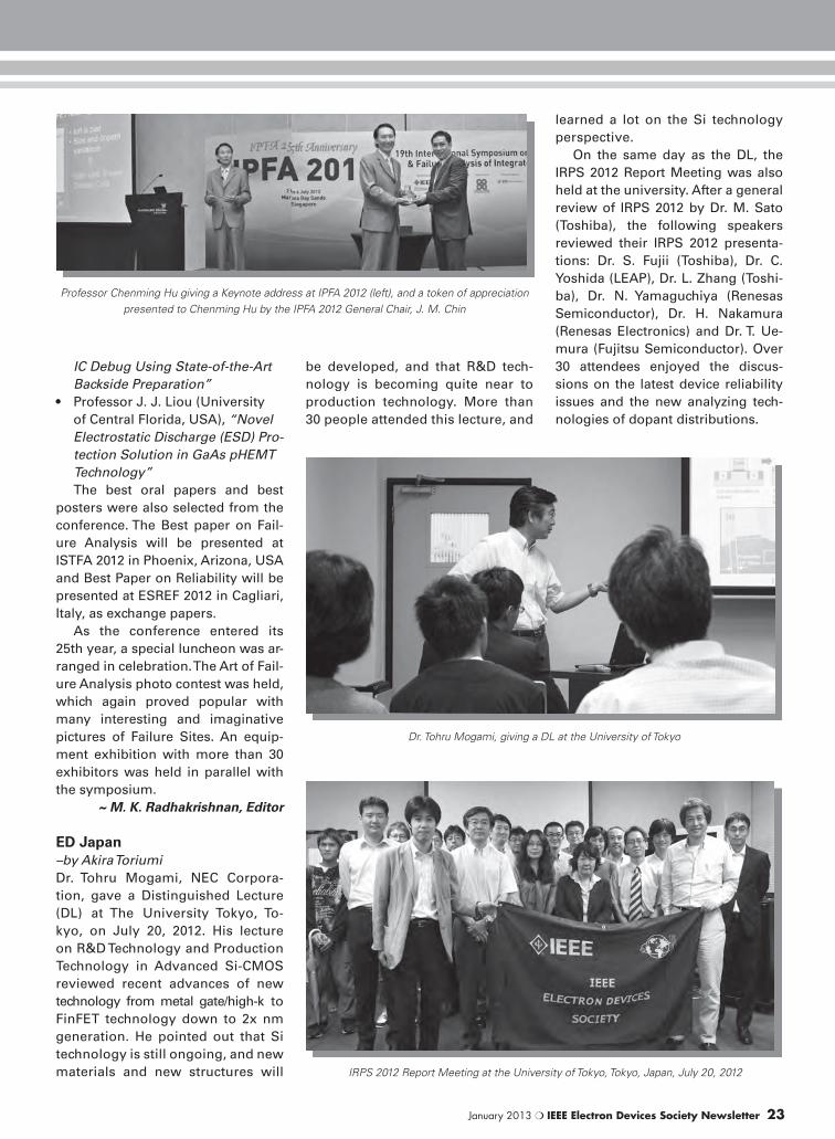
January 2013 ❍ IEEE Electron Devices Society Newsletter 23
IC Debug Using State-of-the-Art
Backside Preparation”
• Professor J. J. Liou (University
of Central Florida, USA), “Novel
Electrostatic Discharge (ESD) Pro-
tection Solution in GaAs pHEMT
Technology”
The best oral papers and best
posters were also selected from the
conference. The Best paper on Fail-
ure Analysis will be presented at
ISTFA 2012 in Phoenix, Arizona, USA
and Best Paper on Reliability will be
presented at ESREF 2012 in Cagliari,
Italy, as exchange papers.
As the conference entered its
25th year, a special luncheon was ar-
ranged in celebration. The Art of Fail-
ure Analysis photo contest was held,
which again proved popular with
many interesting and imaginative
pictures of Failure Sites. An equip-
ment exhibition with more than 30
exhibitors was held in parallel with
the symposium.
~ M. K. Radhakrishnan, Editor
ED Japan–by Akira Toriumi
Dr. Tohru Mogami, NEC Corpora-
tion, gave a Distinguished Lecture
(DL) at The University Tokyo, To-
kyo, on July 20, 2012. His lecture
on R&D Technology and Production
Technology in Advanced Si-CMOS
reviewed recent advances of new
technology from metal gate/high-k to
FinFET technology down to 2x nm
generation. He pointed out that Si
technology is still ongoing, and new
materials and new structures will
be developed, and that R&D tech-
nology is becoming quite near to
production technology. More than
30 people attended this lecture, and
learned a lot on the Si technology
perspective.
On the same day as the DL, the
IRPS 2012 Report Meeting was also
held at the university. After a general
review of IRPS 2012 by Dr. M. Sato
(Toshiba), the following speakers
reviewed their IRPS 2012 presenta-
tions: Dr. S. Fujii (Toshiba), Dr. C.
Yoshida (LEAP), Dr. L. Zhang (Toshi-
ba), Dr. N. Yamaguchiya (Renesas
Semiconductor), Dr. H. Nakamura
(Renesas Electronics) and Dr. T. Ue-
mura (Fujitsu Semiconductor). Over
30 attendees enjoyed the discus-
sions on the latest device reliability
issues and the new analyzing tech-
nologies of dopant distributions.
Professor Chenming Hu giving a Keynote address at IPFA 2012 (left), and a token of appreciation presented to Chenming Hu by the IPFA 2012 General Chair, J. M. Chin
Dr. Tohru Mogami, giving a DL at the University of Tokyo
IRPS 2012 Report Meeting at the University of Tokyo, Tokyo, Japan, July 20, 2012
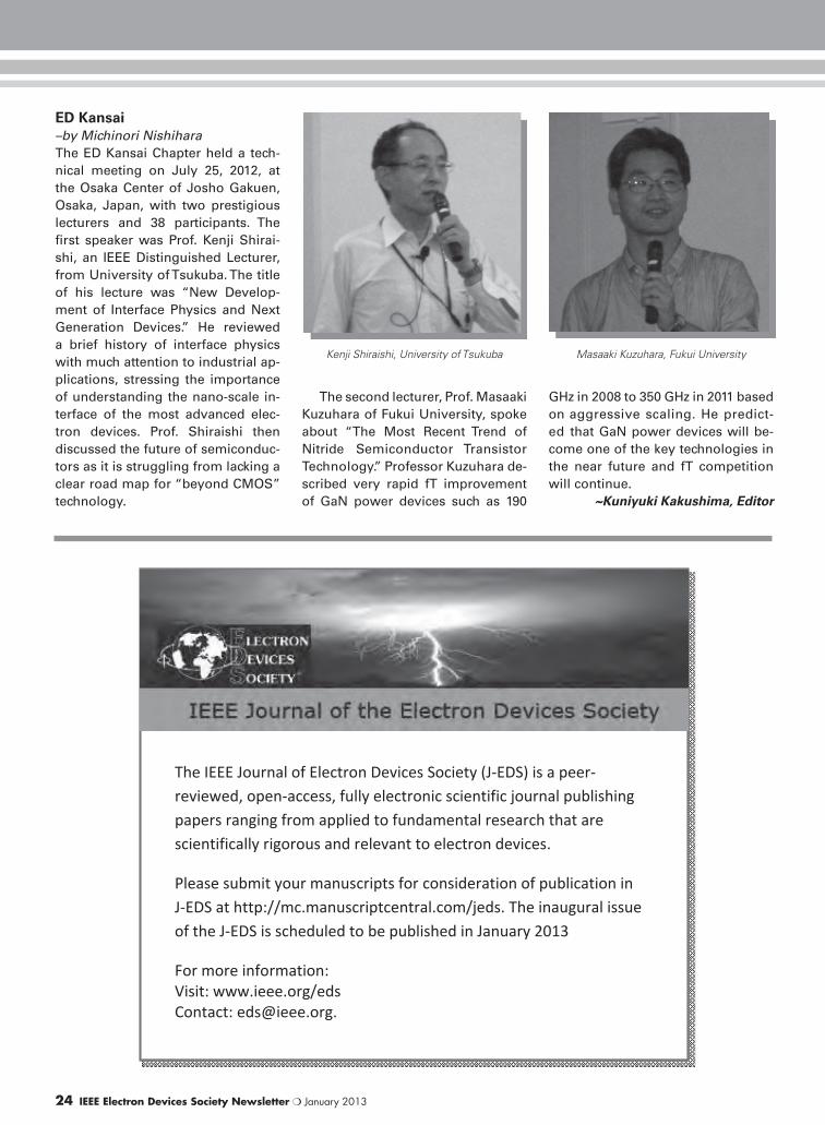
24 IEEE Electron Devices Society Newsletter ❍ January 2013
ED Kansai–by Michinori Nishihara
The ED Kansai Chapter held a tech-
nical meeting on July 25, 2012, at
the Osaka Center of Josho Gakuen,
Osaka, Japan, with two prestigious
lecturers and 38 participants. The
first speaker was Prof. Kenji Shirai-
shi, an IEEE Distinguished Lecturer,
from University of Tsukuba. The title
of his lecture was “New Develop-
ment of Interface Physics and Next
Generation Devices.” He reviewed
a brief history of interface physics
with much attention to industrial ap-
plications, stressing the importance
of understanding the nano-scale in-
terface of the most advanced elec-
tron devices. Prof. Shiraishi then
discussed the future of semiconduc-
tors as it is struggling from lacking a
clear road map for “beyond CMOS”
technology.
The second lecturer, Prof. Masaaki
Kuzuhara of Fukui University, spoke
about “The Most Recent Trend of
Nitride Semiconductor Transistor
Technology.” Professor Kuzuhara de-
scribed very rapid fT improvement
of GaN power devices such as 190
GHz in 2008 to 350 GHz in 2011 based
on aggressive scaling. He predict-
ed that GaN power devices will be-
come one of the key technologies in
the near future and fT competition
will continue.
~Kuniyuki Kakushima, Editor
Kenji Shiraishi, University of Tsukuba Masaaki Kuzuhara, Fukui University
The IEEE Journal of Electron Devices Society (J-EDS) is a peer-reviewed, open-access, fully electronic scientific journal publishing papers ranging from applied to fundamental research that are scientifically rigorous and relevant to electron devices.
Please submit your manuscripts for consideration of publication in J-EDS at http://mc.manuscriptcentral.com/jeds. The inaugural issue of the J-EDS is scheduled to be published in January 2013
For more information: Visit: www.ieee.org/eds Contact: [email protected].
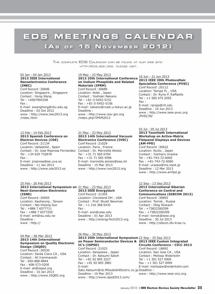
January 2013 ❍ IEEE Electron Devices Society Newsletter 25
THE COMPLETE EDS CALENDAR CAN BE FOUND AT OUR WEB SITE: HTTP://EDS.IEEE.ORG. PLEASE VISIT.
EDS MEET INGS CALENDAR(A S O F 15 N O V E M B E R 2012 )
02 Jan - 04 Jan 20132013 IEEE InternationalNanoelectronics Conference(INEC)Conf Record :20696Location: Singapore , SingaporeContact : Hong WangTel : +6567904358Fax :E-mail: [email protected] : 02 Oct 2012www : http://www.inec2013.org/index.html
19 May - 23 May 20132013 25th International Conferenceon Indium Phosphide and RelatedMaterials (IPRM)Conf Record :30689Location: Kobe , JapanContact : Yoshiaki NakanoTel : +81-3-5452-5151Fax : +81-3-5452-5156E-mail: [email protected] :www : http://www.csw-jpn.org/index.php?IPRM2013
16 Jun - 21 Jun 20132013 IEEE 39th PhotovoltaicSpecialists Conference (PVSC)Conf Record :20112Location: Tampa FL , USAContact : Dr. Ryne P. RaffaelleTel : +1 585 475 2055Fax :E-mail: [email protected] : 10 Jun 2013www : http://www.ieee-pvsc.org/PVSC39/
12 Feb - 14 Feb 20132013 Spanish Conference onElectron Devices (CDE)Conf Record :21134Location: Valladolid , SpainContact : Dr. Jose Represa FernandezTel : +34 629 732878Fax :E-mail: [email protected] : 11 Jan 2013www : http://www.cde2013.es
21 May - 23 May 20132013 14th International VacuumElectronics Conference (IVEC)Conf Record :21029Location: Paris , FranceContact : Dr. Marinella AloisioTel : +31 71 565 6704Fax : +31 71 565 4596E-mail: [email protected] : 15 Mar 2013www : http://www.ivec2013.org
02 Jul - 05 Jul 20132013 Twentieth InternationalWorkshop on Active-MatrixFlatpanel Displays and Devices(AM-FPD)Conf Record :30622Location: Kyoto , JapanContact : Yukiharu UraokaTel : +81-743-72-6060Fax : +81-743-72-6060E-mail: [email protected] : 12 Mar 2013www : http://www.amfpd.jp
25 Feb - 26 Feb 20132013 International Symposium onNext-Generation Electronics(ISNE)Conf Record :20005Location: Kaohsiung , TaiwanContact : Nai-Hsiang SunTel : +886 7 6577711Fax : +886 7 6577205E-mail: [email protected] :www : http://
21 May - 23 May 20132013 IEEE EnergytechConf Record :21305Location: Cleveland OH , USAContact : Prof. Wyatt NewmanTel : +1 216 368 6432Fax :E-mail: [email protected] : 01 Apr 2013www : http://energyTech2013.org
12 Sep - 13 Sep 20132013 International SiberianConference on Control andCommunications (SIBCON 2013)Conf Record :30855Location: Tomsk , RussiaContact : Oleg StukachTel : +73822260299Fax : +73822260299E-mail: [email protected] : 30 Jul 2013www : http://sibcon.sfu-kras.ru
04 Mar - 06 Mar 20132013 14th InternationalSymposium on Quality ElectronicDesign (ISQED)Conf Record :30530Location: Santa Clara CA , USAContact : Ali IranmaneshTel : 650-868-8844Fax : 408-573-0200E-mail: [email protected] : 10 Jan 2013www : http://www.ISQED.org
26 May - 30 May 20132013 25th International Symposiumon Power Semiconductor Devices &IC's (ISPSD)Conf Record :21023Location: Kanazawa , JapanContact : Dr. Katsumi SatohTel : +81 92 805 3227Fax : +81 92 805 3881E-mail:[email protected] : 10 Mar 2013www : http://www.ispsd2013.com/
22 Sep - 25 Sep 20132013 IEEE Custom IntegratedCircuits Conference - CICC 2013Conf Record :18692Location: San Jose CA , USAContact : Melissa WiderkehrTel : +1 301 527 0900Fax : +1 301 527 0994E-mail: [email protected] :www : http://www.ieee-cicc.org
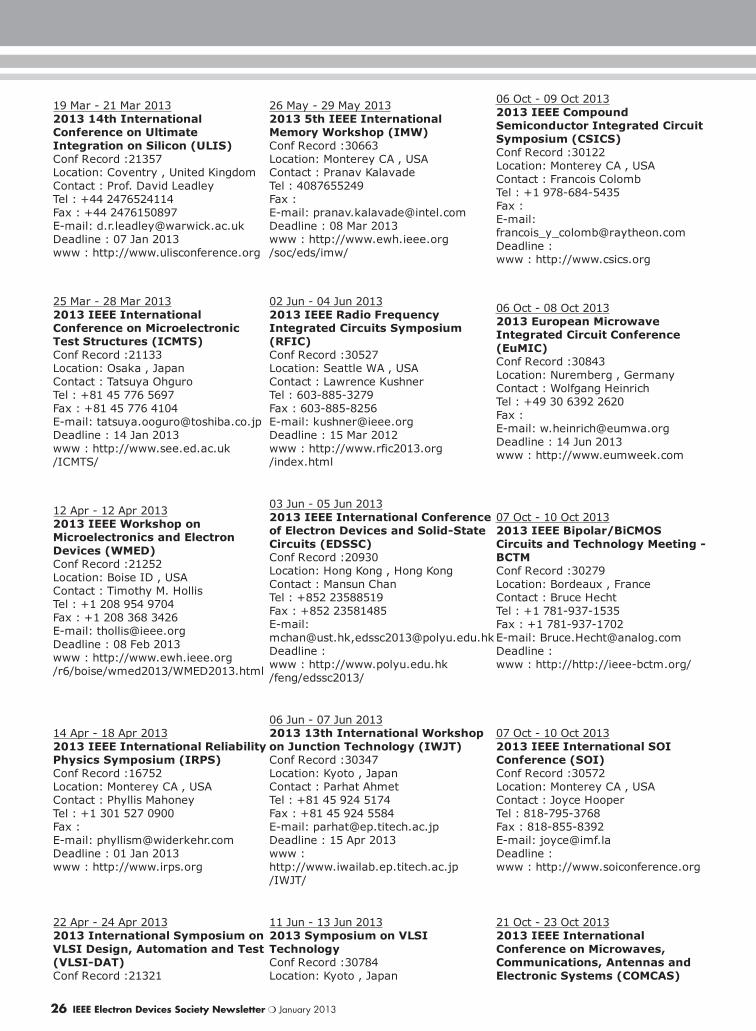
26 IEEE Electron Devices Society Newsletter ❍ January 2013
19 Mar - 21 Mar 20132013 14th InternationalConference on UltimateIntegration on Silicon (ULIS)Conf Record :21357Location: Coventry , United KingdomContact : Prof. David LeadleyTel : +44 2476524114Fax : +44 2476150897E-mail: [email protected] : 07 Jan 2013www : http://www.ulisconference.org
26 May - 29 May 20132013 5th IEEE InternationalMemory Workshop (IMW)Conf Record :30663Location: Monterey CA , USAContact : Pranav KalavadeTel : 4087655249Fax :E-mail: [email protected] : 08 Mar 2013www : http://www.ewh.ieee.org/soc/eds/imw/
06 Oct - 09 Oct 20132013 IEEE CompoundSemiconductor Integrated CircuitSymposium (CSICS)Conf Record :30122Location: Monterey CA , USAContact : Francois ColombTel : +1 978-684-5435Fax :E-mail:[email protected] :www : http://www.csics.org
25 Mar - 28 Mar 20132013 IEEE InternationalConference on MicroelectronicTest Structures (ICMTS)Conf Record :21133Location: Osaka , JapanContact : Tatsuya OhguroTel : +81 45 776 5697Fax : +81 45 776 4104E-mail: [email protected] : 14 Jan 2013www : http://www.see.ed.ac.uk/ICMTS/
02 Jun - 04 Jun 20132013 IEEE Radio FrequencyIntegrated Circuits Symposium(RFIC)Conf Record :30527Location: Seattle WA , USAContact : Lawrence KushnerTel : 603-885-3279Fax : 603-885-8256E-mail: [email protected] : 15 Mar 2012www : http://www.rfic2013.org/index.html
06 Oct - 08 Oct 20132013 European MicrowaveIntegrated Circuit Conference(EuMIC)Conf Record :30843Location: Nuremberg , GermanyContact : Wolfgang HeinrichTel : +49 30 6392 2620Fax :E-mail: [email protected] : 14 Jun 2013www : http://www.eumweek.com
12 Apr - 12 Apr 20132013 IEEE Workshop onMicroelectronics and ElectronDevices (WMED)Conf Record :21252Location: Boise ID , USAContact : Timothy M. HollisTel : +1 208 954 9704Fax : +1 208 368 3426E-mail: [email protected] : 08 Feb 2013www : http://www.ewh.ieee.org/r6/boise/wmed2013/WMED2013.html
03 Jun - 05 Jun 20132013 IEEE International Conferenceof Electron Devices and Solid-StateCircuits (EDSSC)Conf Record :20930Location: Hong Kong , Hong KongContact : Mansun ChanTel : +852 23588519Fax : +852 23581485E-mail:[email protected],[email protected] :www : http://www.polyu.edu.hk/feng/edssc2013/
07 Oct - 10 Oct 20132013 IEEE Bipolar/BiCMOSCircuits and Technology Meeting -BCTMConf Record :30279Location: Bordeaux , FranceContact : Bruce HechtTel : +1 781-937-1535Fax : +1 781-937-1702E-mail: [email protected] :www : http://http://ieee-bctm.org/
14 Apr - 18 Apr 20132013 IEEE International ReliabilityPhysics Symposium (IRPS)Conf Record :16752Location: Monterey CA , USAContact : Phyllis MahoneyTel : +1 301 527 0900Fax :E-mail: [email protected] : 01 Jan 2013www : http://www.irps.org
06 Jun - 07 Jun 20132013 13th International Workshopon Junction Technology (IWJT)Conf Record :30347Location: Kyoto , JapanContact : Parhat AhmetTel : +81 45 924 5174Fax : +81 45 924 5584E-mail: [email protected] : 15 Apr 2013www :http://www.iwailab.ep.titech.ac.jp/IWJT/
07 Oct - 10 Oct 20132013 IEEE International SOIConference (SOI)Conf Record :30572Location: Monterey CA , USAContact : Joyce HooperTel : 818-795-3768Fax : 818-855-8392E-mail: [email protected] :www : http://www.soiconference.org
22 Apr - 24 Apr 20132013 International Symposium onVLSI Design, Automation and Test(VLSI-DAT)Conf Record :21321
11 Jun - 13 Jun 20132013 Symposium on VLSITechnologyConf Record :30784Location: Kyoto , Japan
21 Oct - 23 Oct 20132013 IEEE InternationalConference on Microwaves,Communications, Antennas andElectronic Systems (COMCAS)
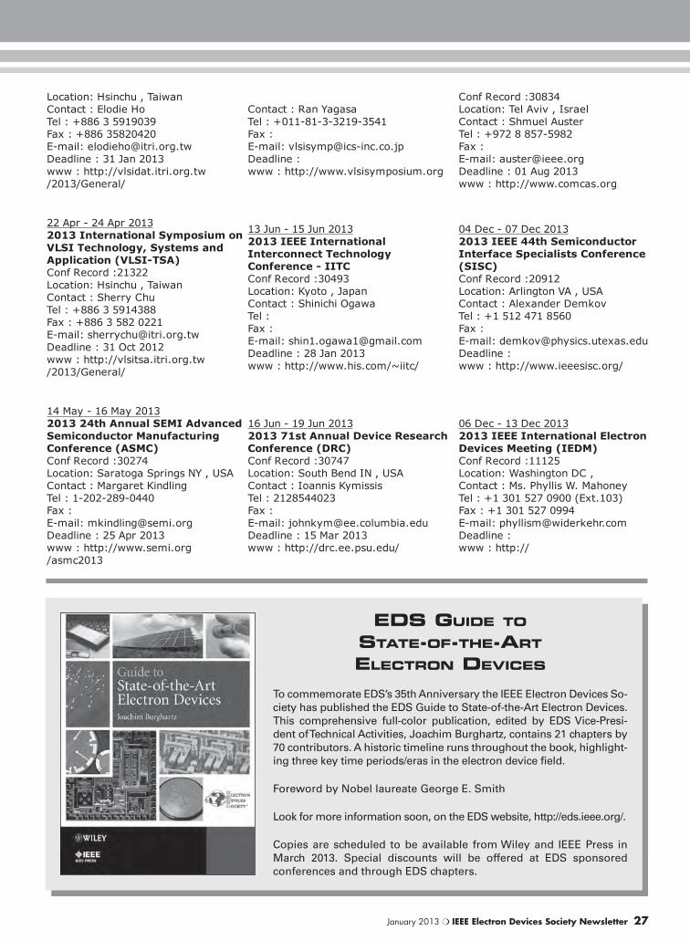
January 2013 ❍ IEEE Electron Devices Society Newsletter 27
Location: Hsinchu , TaiwanContact : Elodie HoTel : +886 3 5919039Fax : +886 35820420E-mail: [email protected] : 31 Jan 2013www : http://vlsidat.itri.org.tw/2013/General/
Contact : Ran YagasaTel : +011-81-3-3219-3541Fax :E-mail: [email protected] :www : http://www.vlsisymposium.org
Conf Record :30834Location: Tel Aviv , IsraelContact : Shmuel AusterTel : +972 8 857-5982Fax :E-mail: [email protected] : 01 Aug 2013www : http://www.comcas.org
22 Apr - 24 Apr 20132013 International Symposium onVLSI Technology, Systems andApplication (VLSI-TSA)Conf Record :21322Location: Hsinchu , TaiwanContact : Sherry ChuTel : +886 3 5914388Fax : +886 3 582 0221E-mail: [email protected] : 31 Oct 2012www : http://vlsitsa.itri.org.tw/2013/General/
13 Jun - 15 Jun 20132013 IEEE InternationalInterconnect TechnologyConference - IITCConf Record :30493Location: Kyoto , JapanContact : Shinichi OgawaTel :Fax :E-mail: [email protected] : 28 Jan 2013www : http://www.his.com/~iitc/
04 Dec - 07 Dec 20132013 IEEE 44th SemiconductorInterface Specialists Conference(SISC)Conf Record :20912Location: Arlington VA , USAContact : Alexander DemkovTel : +1 512 471 8560Fax :E-mail: [email protected] :www : http://www.ieeesisc.org/
14 May - 16 May 20132013 24th Annual SEMI AdvancedSemiconductor ManufacturingConference (ASMC)Conf Record :30274Location: Saratoga Springs NY , USAContact : Margaret KindlingTel : 1-202-289-0440Fax :E-mail: [email protected] : 25 Apr 2013www : http://www.semi.org/asmc2013
16 Jun - 19 Jun 20132013 71st Annual Device ResearchConference (DRC)Conf Record :30747Location: South Bend IN , USAContact : Ioannis KymissisTel : 2128544023Fax :E-mail: [email protected] : 15 Mar 2013www : http://drc.ee.psu.edu/
06 Dec - 13 Dec 20132013 IEEE International ElectronDevices Meeting (IEDM)Conf Record :11125Location: Washington DC ,Contact : Ms. Phyllis W. MahoneyTel : +1 301 527 0900 (Ext.103)Fax : +1 301 527 0994E-mail: [email protected] :www : http://
EDS GUIDE TO STATE-OF-THE-ART
ELECTRON DEVICES
To commemorate EDS’s 35th Anniversary the IEEE Electron Devices So-
ciety has published the EDS Guide to State-of-the-Art Electron Devices.
This comprehensive full-color publication, edited by EDS Vice-Presi-
dent of Technical Activities, Joachim Burghartz, contains 21 chapters by
70 contributors. A historic timeline runs throughout the book, highlight-
ing three key time periods/eras in the electron device field.
Foreword by Nobel laureate George E. Smith
Look for more information soon, on the EDS website, http://eds.ieee.org/.
Copies are scheduled to be available from Wiley and IEEE Press in
March 2013. Special discounts will be offered at EDS sponsored
conferences and through EDS chapters.
28 IEEE Electron Devices Society Newsletter ❍ January 2013
EDS ANNOUNCES ADMINISTRATIVE COMMITTEE NOW BOARD OF GOVERNORS
At the June AdCom meeting in Leuven, Belgium, the ED administrative committee unanimously
voted to change its name to Board of Governors. Recently, the final approval for this change was
granted by IEEE Technical Activities.
Henceforth, the EDS’s AdCom will be known as the EDS Board of Governors or BoG. All roles and
functions of the BoG will remain as they were under the AdCom moniker, however this new name
more accurately reflects the volunteer-led, volunteer-driven spirit of the society and is therefore an
important distinction.
“AdCom” is a well-known, heavily-used term within the society and it will no doubt take some time
for the change to “BoG” to take hold, but look for this transition to begin immediately, starting with
the “AdCom” section of the EDS site in the coming weeks.