supplementary information coaxial lithography...1 supplementary information coaxial lithography...
TRANSCRIPT
1
Supplementary Information
Coaxial Lithography
Tuncay Ozel#, Gilles R. Bourret#, Chad A. Mirkin*
*e-mail: [email protected]
#These authors contributed equally to this work
Materials and chemicals: All chemicals and solutions were used without further processing.
Commercially available plating solutions (Cyless for Ag, Orotemp 24 Rack for Au, Pallaspeed
VHS for Pd, and nickel sulfamate for Ni) were purchased from Technic Inc., USA. Thiophene
(≥99%), 3-hexylthiophene (≥99%), cadmium sulfate (99%), lithium perchlorate (99.99%),
selenium dioxide (99.9%), boron trifluoride diethyl etherate, cadmium chloride (99.99%), sulfur
(≥99.5%), dimethyl sulfoxide (≥99%), aniline (≥99.5%), potassium hydroxide (≥99%),
concentrated perchloric acid (≥99.999%), nitric acid (ACS grade), ammonium hexachloroplatinate
(99.999%), sodium phosphate dibasic (99%), sulfuric acid (ACS grade) and sodium citrate (≥99%)
were purchased from Sigma Aldrich, USA. Manganese acetate was obtained from Alfa.
Nanopure™ water was used. Porous anodized aluminum oxide (AAO) membranes with nominal
pore diameters of 280 nm were purchased from Whatman Inc., USA. AAO membranes with 35,
55 and 100 nm nominal pore diameters were purchased from Synkera Technologies Inc., USA.
Instruments: Secondary electron (SE mode) and high-angle annular dark-field imaging z-contrast
(ZC mode) scanning transmission electron microscope (STEM) images were acquired using a
Hitachi HD-2300 STEM. Electrochemical deposition of metals and inorganic semiconductors
were done using a BASi EC epsilon potentiostat (Bioanalytical Systems, Inc., USA). Instruments
Coaxial lithography
SUPPLEMENTARY INFORMATIONDOI: 10.1038/NNANO.2015.33
NATURE NANOTECHNOLOGY | www.nature.com/naturenanotechnology 1
© 2015 Macmillan Publishers Limited. All rights reserved
2
and methods used for the EDX maps and for the single nanowire measurements are described later
in the text.
Nanowire synthesis: Porous anodized aluminum oxide (AAO) membranes with nominal pore
diameters of 280 nm (Whatman Inc., USA) and of 35, 55, 100 nm (Synkera Technologies Inc.,
USA) were used as templates to synthesize nanowires in a three electrode setup, as described in
detail elsewhere18, 28, 29. The bottom side of the membranes was coated with a 200 nm thick Ag
layer using either thermal or e-beam evaporation. Unless mentioned otherwise, a conventional
three-electrode electrochemical cell was used for the material electrodeposition, with a Pt counter
electrode, an Ag/AgCl reference electrode, while the Ag-coated AAO membrane was used as the
working electrode. The electrochemical cell and electrodes were thoroughly washed in nanopure
water after each deposition steps.
Electrochemical depositions
Metals: Metals were deposited at constant potentials using aqueous plating solutions.
Au was deposited at -930 mV (280 and 100 nm template) and -1100 mV (55 and 35 nm template)
using Orotemp 24 Rack solution.
Ag was deposited at -900 mV using Cyless solution.
Pd was deposited at -900 mV using Pallaspeed VHS solution.
Nickel was deposited at -930 mV (280 nm and 100 nm template) and -1100 mV (55 and 35 nm
template) using nickel sulfamate solution.
Pt was deposited at -520 mV using a homemade aqueous Pt solution (15 mM (NH4)2PtCl6 and 200
mM Na2HPO4).
© 2015 Macmillan Publishers Limited. All rights reserved
3
Polypyrrole (PPy): PPy was deposited at +750 mV, using a homemade solution containg 510 µL
of pyrrole dissolved in 30 mL of a 0.1 M LiClO4 aqueous solution.
Polyaniline (PANI): PANI was deposited at +1000 mV, using a homemade solution containing
680 µL of aniline dissolved in a 15 mL 0.1 M HClO4 aqueous solution.
Polythiophene (PTh) and poly(3-hexylthiophene) (P3HT): PTh and P3HT were deposited using
cyclic voltammetry between -400 and +1100 mV at 400 mV/s. A Pt rod was used as the reference
electrode. The monomers were dissolved in boron trifluoride diethyl etherate (BFEE) which served
as the solvent and the electrolyte10, 31, S1. Prior to the deposition, the electrochemical cell and the
AAO membrane were immersed in ethanol and dried under vacuum to remove any residual water.
CdSe: CdSe was deposited as previously reported using cyclic voltammetry between -387 and -
787 mV vs SCE at 752 mV/sS2. The plating solution was composed of 0.7 mM SeO2, 0.3 M CdSO4,
and 0.25 M H2SO4 . Triton X (0.25% v/v) was added to the solution.
CdS: CdS was deposited as previously reported under constant current (-1.5 mA.cm-2) at 130 °C
in a two electrode configuration24. The plating solution was made by dissolving 1.52 g of CdCl2
and 914 mg of S in 150 mL of hot DMSO.
MnO2: MnO2 was deposited according to the literature at +750 mV using an aqueous solution of
manganese acetate (49 mg of manganese acetate was dissolved in 20 mL of water)S3.
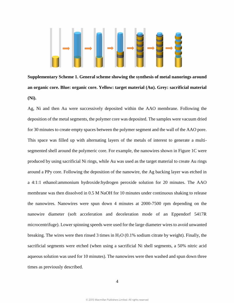
Approach #1: synthesis of a polymer core with metal nanorings
© 2015 Macmillan Publishers Limited. All rights reserved
4
Supplementary Scheme 1. General scheme showing the synthesis of metal nanorings around
an organic core. Blue: organic core. Yellow: target material (Au). Grey: sacrificial material
(Ni).
Ag, Ni and then Au were successively deposited within the AAO membrane. Following the
deposition of the metal segments, the polymer core was deposited. The samples were vacuum dried
for 30 minutes to create empty spaces between the polymer segment and the wall of the AAO pore.
This space was filled up with alternating layers of the metals of interest to generate a multi-
segmented shell around the polymeric core. For example, the nanowires shown in Figure 1C were
produced by using sacrificial Ni rings, while Au was used as the target material to create Au rings
around a PPy core. Following the deposition of the nanowire, the Ag backing layer was etched in
a 4:1:1 ethanol:ammonium hydroxide:hydrogen peroxide solution for 20 minutes. The AAO
membrane was then dissolved in 0.5 M NaOH for 10 minutes under continuous shaking to release
the nanowires. Nanowires were spun down 4 minutes at 2000-7500 rpm depending on the
nanowire diameter (soft acceleration and deceleration mode of an Eppendorf 5417R
microcentrifuge). Lower spinning speeds were used for the large diameter wires to avoid unwanted
breaking. The wires were then rinsed 3 times in H2O (0.1% sodium citrate by weight). Finally, the
sacrificial segments were etched (when using a sacrificial Ni shell segments, a 50% nitric acid
aqueous solution was used for 10 minutes). The nanowires were then washed and spun down three
times as previously described.
© 2015 Macmillan Publishers Limited. All rights reserved
5
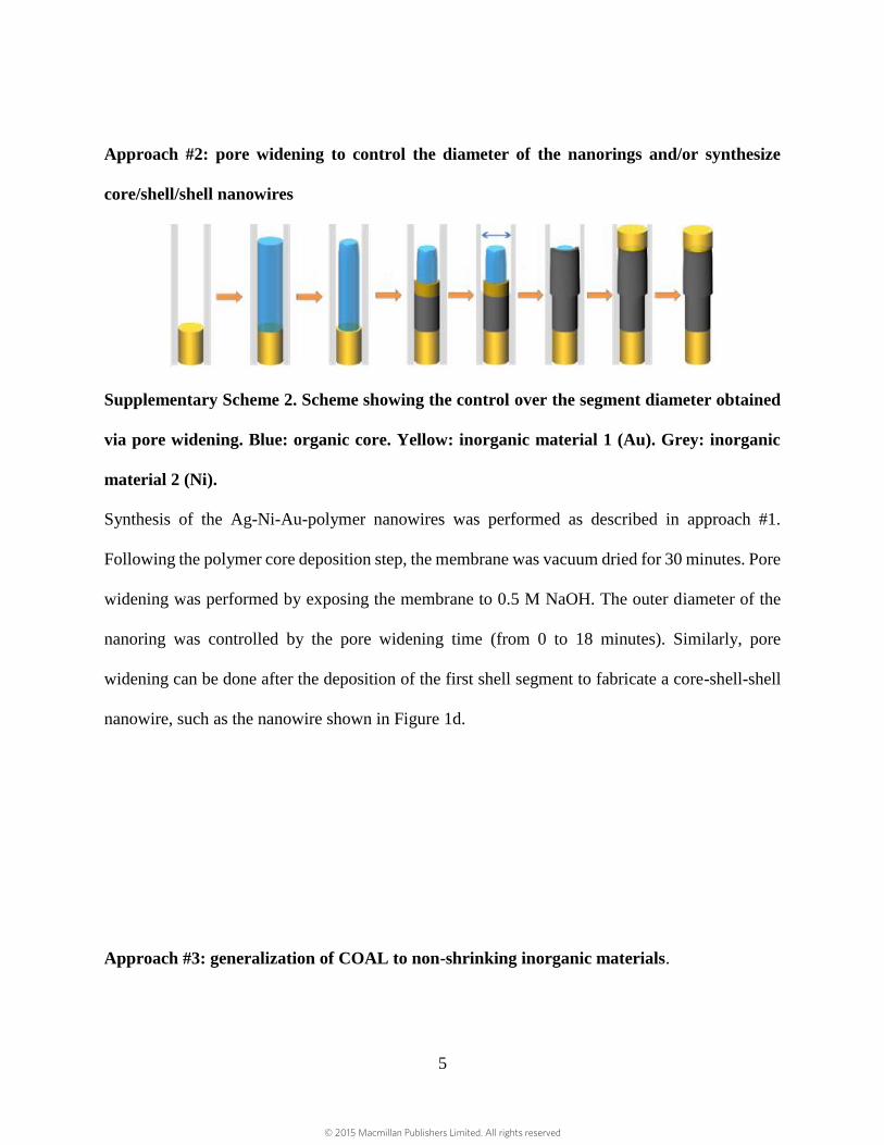
Approach #2: pore widening to control the diameter of the nanorings and/or synthesize
core/shell/shell nanowires
Supplementary Scheme 2. Scheme showing the control over the segment diameter obtained
via pore widening. Blue: organic core. Yellow: inorganic material 1 (Au). Grey: inorganic
material 2 (Ni).
Synthesis of the Ag-Ni-Au-polymer nanowires was performed as described in approach #1.
Following the polymer core deposition step, the membrane was vacuum dried for 30 minutes. Pore
widening was performed by exposing the membrane to 0.5 M NaOH. The outer diameter of the
nanoring was controlled by the pore widening time (from 0 to 18 minutes). Similarly, pore
widening can be done after the deposition of the first shell segment to fabricate a core-shell-shell
nanowire, such as the nanowire shown in Figure 1d.
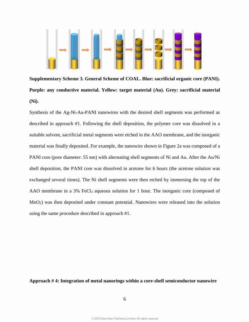
Approach #3: generalization of COAL to non-shrinking inorganic materials.
© 2015 Macmillan Publishers Limited. All rights reserved
6
Supplementary Scheme 3. General Scheme of COAL. Blue: sacrificial organic core (PANI).
Purple: any conductive material. Yellow: target material (Au). Grey: sacrificial material
(Ni).
Synthesis of the Ag-Ni-Au-PANI nanowires with the desired shell segments was performed as
described in approach #1. Following the shell deposition, the polymer core was dissolved in a
suitable solvent, sacrificial metal segments were etched in the AAO membrane, and the inorganic
material was finally deposited. For example, the nanowire shown in Figure 2a was composed of a
PANI core (pore diameter: 55 nm) with alternating shell segments of Ni and Au. After the Au/Ni
shell deposition, the PANI core was dissolved in acetone for 6 hours (the acetone solution was
exchanged several times). The Ni shell segments were then etched by immersing the top of the
AAO membrane in a 3% FeCl3 aqueous solution for 1 hour. The inorganic core (composed of
MnO2) was then deposited under constant potential. Nanowires were released into the solution
using the same procedure described in approach #1.
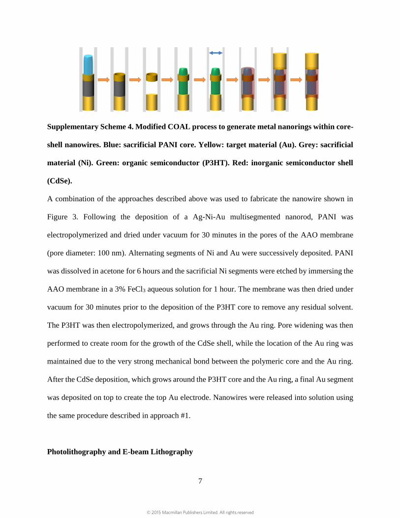
Approach # 4: Integration of metal nanorings within a core-shell semiconductor nanowire
© 2015 Macmillan Publishers Limited. All rights reserved
7
Supplementary Scheme 4. Modified COAL process to generate metal nanorings within core-
shell nanowires. Blue: sacrificial PANI core. Yellow: target material (Au). Grey: sacrificial
material (Ni). Green: organic semiconductor (P3HT). Red: inorganic semiconductor shell
(CdSe).
A combination of the approaches described above was used to fabricate the nanowire shown in
Figure 3. Following the deposition of a Ag-Ni-Au multisegmented nanorod, PANI was
electropolymerized and dried under vacuum for 30 minutes in the pores of the AAO membrane
(pore diameter: 100 nm). Alternating segments of Ni and Au were successively deposited. PANI
was dissolved in acetone for 6 hours and the sacrificial Ni segments were etched by immersing the
AAO membrane in a 3% FeCl3 aqueous solution for 1 hour. The membrane was then dried under
vacuum for 30 minutes prior to the deposition of the P3HT core to remove any residual solvent.
The P3HT was then electropolymerized, and grows through the Au ring. Pore widening was then
performed to create room for the growth of the CdSe shell, while the location of the Au ring was
maintained due to the very strong mechanical bond between the polymeric core and the Au ring.
After the CdSe deposition, which grows around the P3HT core and the Au ring, a final Au segment
was deposited on top to create the top Au electrode. Nanowires were released into solution using
the same procedure described in approach #1.
Photolithography and E-beam Lithography
© 2015 Macmillan Publishers Limited. All rights reserved
8
Si wafer with a 500 nm oxide coating was spin-coated at 500 rpm for 10 s and at 4000 rpm for 40
s with a layer of S1805 photoresist (Shipley, USA) and was annealed at 115 °C for 1 min.
Patterning on the resist was made using a Microtech MA6 Aligner mask aligner (Süss, Germany)
and the patterns were developed with MF-24A (Microchem, USA) for 1 min. For the electrode
pad fabrication, 5 nm of Cr and 100 nm of Au were evaporated and the photoresist and excess
metal layer were lifted off using Remover PG (Microchem, USA) overnight. Multi-segmented
nanowires were drop-casted on the patterned Si chips on a hot plate at 70 °C and left for drying
for 5 minutes. Metal electrodes on the Si chip and the nanorod electrode segments on the nanowires
were bridged using Quanta FESEM (FEI, USA) electron beam lithography (EBL). Si wafers with
well dispersed nanowires were spin-coated at 500 rpm for 10 s and at 3000 rpm for 45 s with a
layer of 950 PMMA C7 e-beam resist (Microchem, USA) and annealed at 180 °C for 2 min. Fine
patterning was done using the Nanometer Pattern Generation System (NPGS, JC Nabity
Lithography System, Bozeman, MT, USA) at 30 kV acceleration voltage and the patterns were
developed with 3:1 IPA/MIBK solution for 1 min. 3 nm of Cr and 75 nm of Au films were
evaporated and the excess materials were lifted off overnight in acetone.
Supplementary Figures
© 2015 Macmillan Publishers Limited. All rights reserved
9
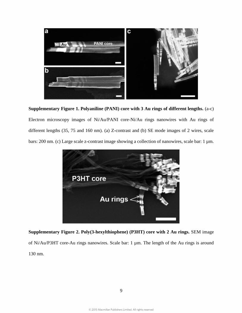
Supplementary Figure 1. Polyaniline (PANI) core with 3 Au rings of different lengths. (a-c)
Electron microscopy images of Ni/Au/PANI core-Ni/Au rings nanowires with Au rings of
different lengths (35, 75 and 160 nm). (a) Z-contrast and (b) SE mode images of 2 wires, scale
bars: 200 nm. (c) Large scale z-contrast image showing a collection of nanowires, scale bar: 1 µm.
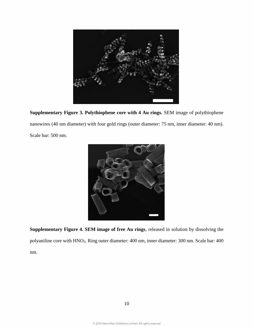
Supplementary Figure 2. Poly(3-hexylthiophene) (P3HT) core with 2 Au rings. SEM image
of Ni/Au/P3HT core-Au rings nanowires. Scale bar: 1 µm. The length of the Au rings is around
130 nm.
© 2015 Macmillan Publishers Limited. All rights reserved
10
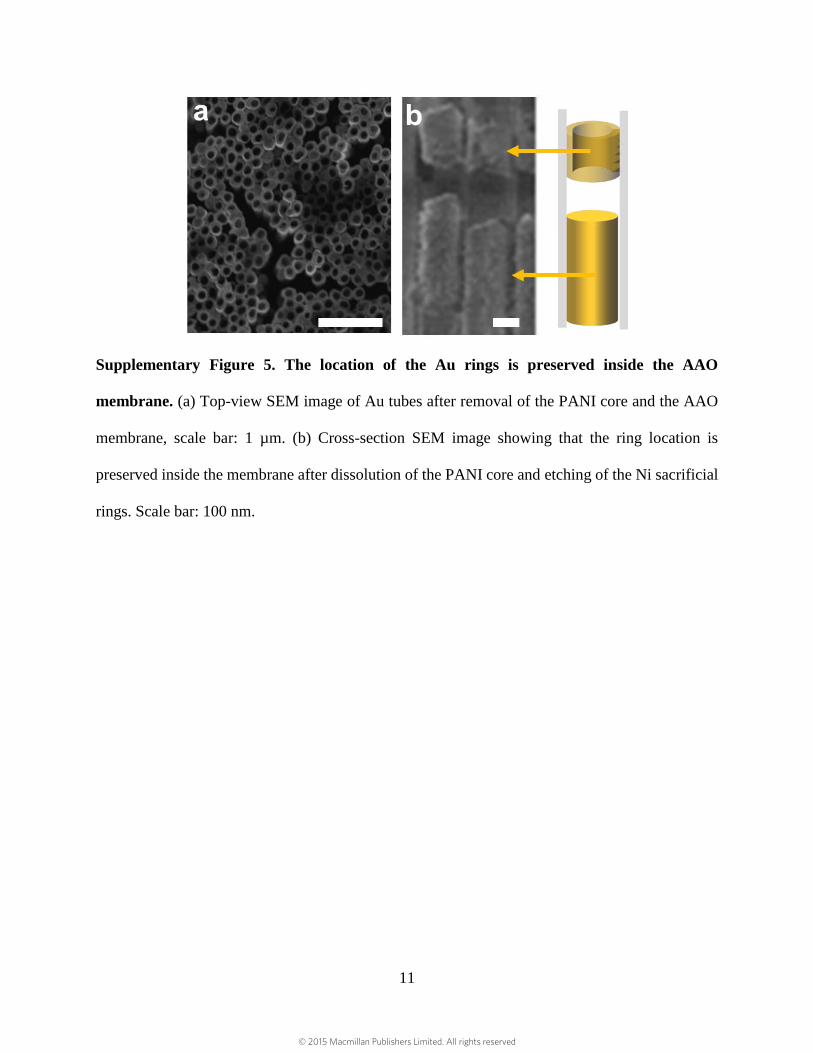
Supplementary Figure 3. Polythiophene core with 4 Au rings. SEM image of polythiophene
nanowires (40 nm diameter) with four gold rings (outer diameter: 75 nm, inner diameter: 40 nm).
Scale bar: 500 nm.
Supplementary Figure 4. SEM image of free Au rings, released in solution by dissolving the
polyaniline core with HNO3. Ring outer diameter: 400 nm, inner diameter: 300 nm. Scale bar: 400
nm.
© 2015 Macmillan Publishers Limited. All rights reserved
11
Supplementary Figure 5. The location of the Au rings is preserved inside the AAO
membrane. (a) Top-view SEM image of Au tubes after removal of the PANI core and the AAO
membrane, scale bar: 1 µm. (b) Cross-section SEM image showing that the ring location is
preserved inside the membrane after dissolution of the PANI core and etching of the Ni sacrificial
rings. Scale bar: 100 nm.
© 2015 Macmillan Publishers Limited. All rights reserved
12
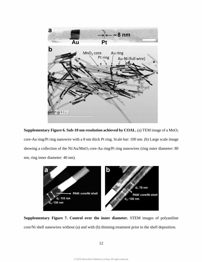
Supplementary Figure 6. Sub-10 nm resolution achieved by COAL. (a) TEM image of a MnO2
core-Au ring/Pt ring nanowire with a 8 nm thick Pt ring. Scale bar: 100 nm. (b) Large scale image
showing a collection of the Ni/Au/MnO2 core-Au ring/Pt ring nanowires (ring outer diameter: 80
nm, ring inner diameter: 40 nm).
Supplementary Figure 7. Control over the inner diameter. STEM images of polyaniline
core/Ni shell nanowires without (a) and with (b) thinning treatment prior to the shell deposition.
© 2015 Macmillan Publishers Limited. All rights reserved
13
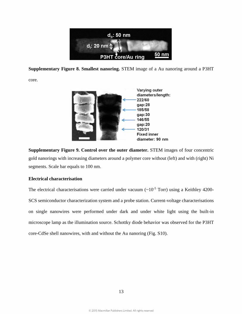
Supplementary Figure 8. Smallest nanoring. STEM image of a Au nanoring around a P3HT
core.
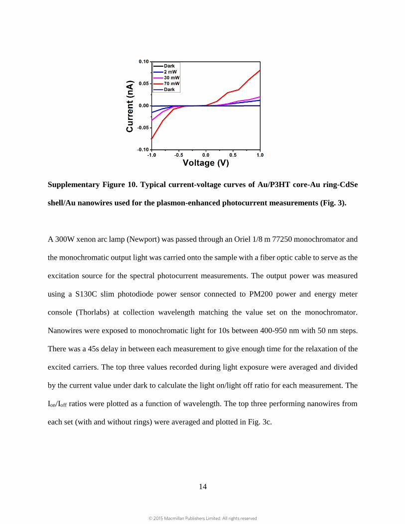
Supplementary Figure 9. Control over the outer diameter. STEM images of four concentric
gold nanorings with increasing diameters around a polymer core without (left) and with (right) Ni
segments. Scale bar equals to 100 nm.
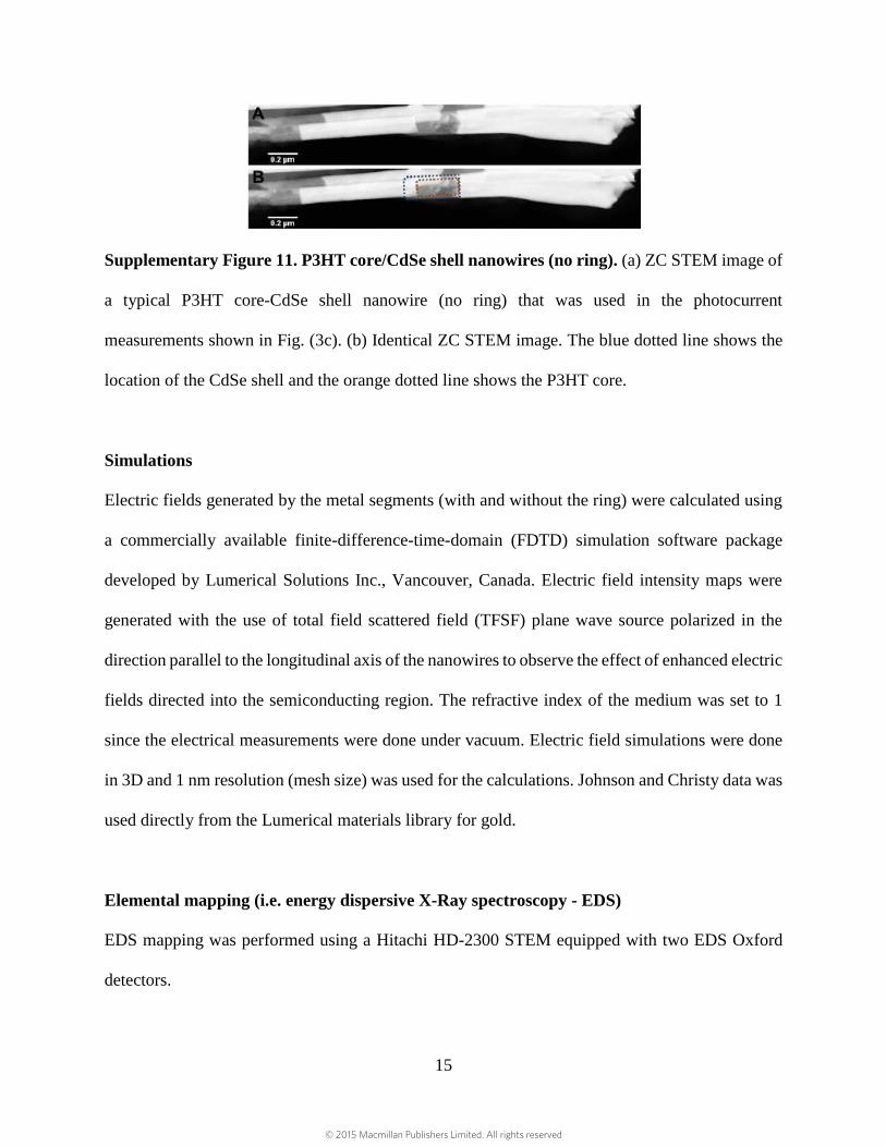
Electrical characterisation
The electrical characterisations were carried under vacuum (~10-5 Torr) using a Keithley 4200-
SCS semiconductor characterization system and a probe station. Current-voltage characterisations
on single nanowires were performed under dark and under white light using the built-in
microscope lamp as the illumination source. Schottky diode behavior was observed for the P3HT
core-CdSe shell nanowires, with and without the Au nanoring (Fig. S10).
© 2015 Macmillan Publishers Limited. All rights reserved
14
Supplementary Figure 10. Typical current-voltage curves of Au/P3HT core-Au ring-CdSe
shell/Au nanowires used for the plasmon-enhanced photocurrent measurements (Fig. 3).
A 300W xenon arc lamp (Newport) was passed through an Oriel 1/8 m 77250 monochromator and
the monochromatic output light was carried onto the sample with a fiber optic cable to serve as the
excitation source for the spectral photocurrent measurements. The output power was measured
using a S130C slim photodiode power sensor connected to PM200 power and energy meter
console (Thorlabs) at collection wavelength matching the value set on the monochromator.
Nanowires were exposed to monochromatic light for 10s between 400-950 nm with 50 nm steps.
There was a 45s delay in between each measurement to give enough time for the relaxation of the
excited carriers. The top three values recorded during light exposure were averaged and divided
by the current value under dark to calculate the light on/light off ratio for each measurement. The
Ion/Ioff ratios were plotted as a function of wavelength. The top three performing nanowires from
each set (with and without rings) were averaged and plotted in Fig. 3c.
© 2015 Macmillan Publishers Limited. All rights reserved
15
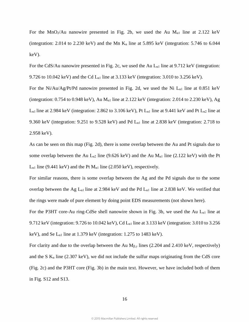
Supplementary Figure 11. P3HT core/CdSe shell nanowires (no ring). (a) ZC STEM image of
a typical P3HT core-CdSe shell nanowire (no ring) that was used in the photocurrent
measurements shown in Fig. (3c). (b) Identical ZC STEM image. The blue dotted line shows the
location of the CdSe shell and the orange dotted line shows the P3HT core.
Simulations
Electric fields generated by the metal segments (with and without the ring) were calculated using
a commercially available finite-difference-time-domain (FDTD) simulation software package
developed by Lumerical Solutions Inc., Vancouver, Canada. Electric field intensity maps were
generated with the use of total field scattered field (TFSF) plane wave source polarized in the
direction parallel to the longitudinal axis of the nanowires to observe the effect of enhanced electric
fields directed into the semiconducting region. The refractive index of the medium was set to 1
since the electrical measurements were done under vacuum. Electric field simulations were done
in 3D and 1 nm resolution (mesh size) was used for the calculations. Johnson and Christy data was
used directly from the Lumerical materials library for gold.
Elemental mapping (i.e. energy dispersive X-Ray spectroscopy - EDS)
EDS mapping was performed using a Hitachi HD-2300 STEM equipped with two EDS Oxford
detectors.
© 2015 Macmillan Publishers Limited. All rights reserved
16
For the MnO2/Au nanowire presented in Fig. 2b, we used the Au Mα1 line at 2.122 keV
(integration: 2.014 to 2.230 keV) and the Mn Kα line at 5.895 keV (integration: 5.746 to 6.044
keV).
For the CdS/Au nanowire presented in Fig. 2c, we used the Au Lα1 line at 9.712 keV (integration:
9.726 to 10.042 keV) and the Cd Lα1 line at 3.133 keV (integration: 3.010 to 3.256 keV).
For the Ni/Au/Ag/Pt/Pd nanowire presented in Fig. 2d, we used the Ni Lα1 line at 0.851 keV
(integration: 0.754 to 0.948 keV), Au Mα1 line at 2.122 keV (integration: 2.014 to 2.230 keV), Ag
Lα1 line at 2.984 keV (integration: 2.862 to 3.106 keV), Pt Lα1 line at 9.441 keV and Pt Lα2 line at
9.360 keV (integration: 9.251 to 9.528 keV) and Pd Lα1 line at 2.838 keV (integration: 2.718 to
2.958 keV).
As can be seen on this map (Fig. 2d), there is some overlap between the Au and Pt signals due to
some overlap between the Au Lα2 line (9.626 keV) and the Au Mα1 line (2.122 keV) with the Pt
Lα1 line (9.441 keV) and the Pt Mα1 line (2.050 keV), respectively.
For similar reasons, there is some overlap between the Ag and the Pd signals due to the some
overlap between the Ag Lα1 line at 2.984 keV and the Pd Lα1 line at 2.838 keV. We verified that
the rings were made of pure element by doing point EDS measurements (not shown here).
For the P3HT core-Au ring-CdSe shell nanowire shown in Fig. 3b, we used the Au Lα1 line at
9.712 keV (integration: 9.726 to 10.042 keV), Cd Lα1 line at 3.133 keV (integration: 3.010 to 3.256
keV), and Se Lα1 line at 1.379 keV (integration: 1.275 to 1483 keV).
For clarity and due to the overlap between the Au Mβ,γ lines (2.204 and 2.410 keV, respectively)
and the S Kα line (2.307 keV), we did not include the sulfur maps originating from the CdS core
(Fig. 2c) and the P3HT core (Fig. 3b) in the main text. However, we have included both of them
in Fig. S12 and S13.
© 2015 Macmillan Publishers Limited. All rights reserved
17
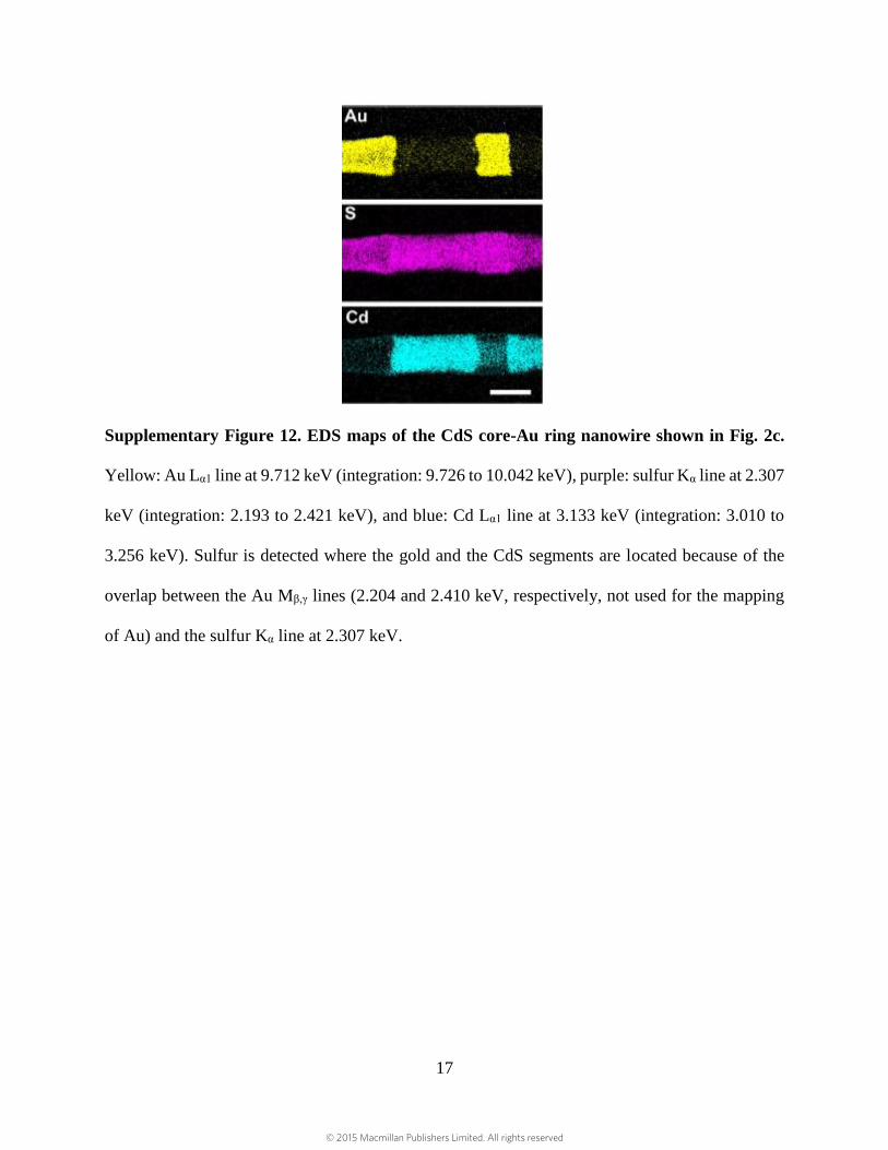
Supplementary Figure 12. EDS maps of the CdS core-Au ring nanowire shown in Fig. 2c.
Yellow: Au Lα1 line at 9.712 keV (integration: 9.726 to 10.042 keV), purple: sulfur Kα line at 2.307
keV (integration: 2.193 to 2.421 keV), and blue: Cd Lα1 line at 3.133 keV (integration: 3.010 to
3.256 keV). Sulfur is detected where the gold and the CdS segments are located because of the
overlap between the Au Mβ,γ lines (2.204 and 2.410 keV, respectively, not used for the mapping
of Au) and the sulfur Kα line at 2.307 keV.
© 2015 Macmillan Publishers Limited. All rights reserved
18
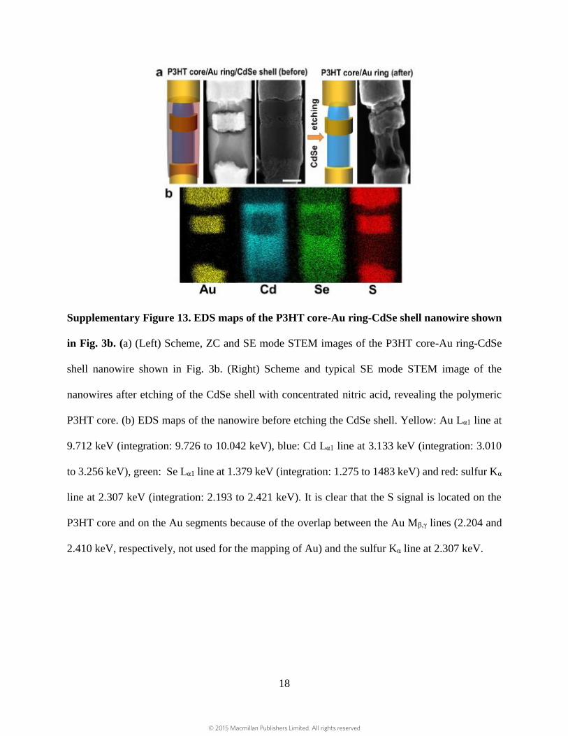
Supplementary Figure 13. EDS maps of the P3HT core-Au ring-CdSe shell nanowire shown
in Fig. 3b. (a) (Left) Scheme, ZC and SE mode STEM images of the P3HT core-Au ring-CdSe
shell nanowire shown in Fig. 3b. (Right) Scheme and typical SE mode STEM image of the
nanowires after etching of the CdSe shell with concentrated nitric acid, revealing the polymeric
P3HT core. (b) EDS maps of the nanowire before etching the CdSe shell. Yellow: Au Lα1 line at
9.712 keV (integration: 9.726 to 10.042 keV), blue: Cd Lα1 line at 3.133 keV (integration: 3.010
to 3.256 keV), green: Se Lα1 line at 1.379 keV (integration: 1.275 to 1483 keV) and red: sulfur Kα
line at 2.307 keV (integration: 2.193 to 2.421 keV). It is clear that the S signal is located on the
P3HT core and on the Au segments because of the overlap between the Au Mβ,γ lines (2.204 and
2.410 keV, respectively, not used for the mapping of Au) and the sulfur Kα line at 2.307 keV.
© 2015 Macmillan Publishers Limited. All rights reserved
19
References
S1. O'Carroll, D. M., Hofmann, C. E. & Atwater, H. A. Conjugated polymer/metal nanowire
heterostructure plasmonic antennas. Adv. Mater. 22, 1223-1227 (2010).
S2. Schierhorn, M., Boettcher, S. W., Kraemer, S., Stucky, G. D. & Moskovits, M.
Photoelectrochemical performance of CdSe nanorod arrays grown on a transparent
conducting substrate. Nano Lett. 9, 3262-3267 (2009).
S3. Liu, R. & Lee, S. B. MnO2/Poly(3,4-ethylenedioxythiophene) coaxial nanowires by one-
step coelectrodeposition for electrochemical energy storage. J. Am. Chem. Soc. 130, 2942-
2943 (2008).
© 2015 Macmillan Publishers Limited. All rights reserved