super audio cd player pd-d6-j · pdf filepioneer electronics asiacentre pte. ltd. 253...
TRANSCRIPT
PIONEER CORPORATION 4-1, Meguro 1-chome,PIONEER ELECTRONICS (USA) INC. P.O. Box 1760, LonPIONEER EUROPE NV Haven 1087, Keetberglaan 1, 912PIONEER ELECTRONICS ASIACENTRE PTE. LTD. 253
PIONEER CORPORATION 2006
PD-D6-J
Meguro-ku, Tokyo 153-8654, Japang Beach, CA 90801-1760, U.S.A.
0 Melsele, BelgiumAlexandra Road, #04-01, Singapore 159936
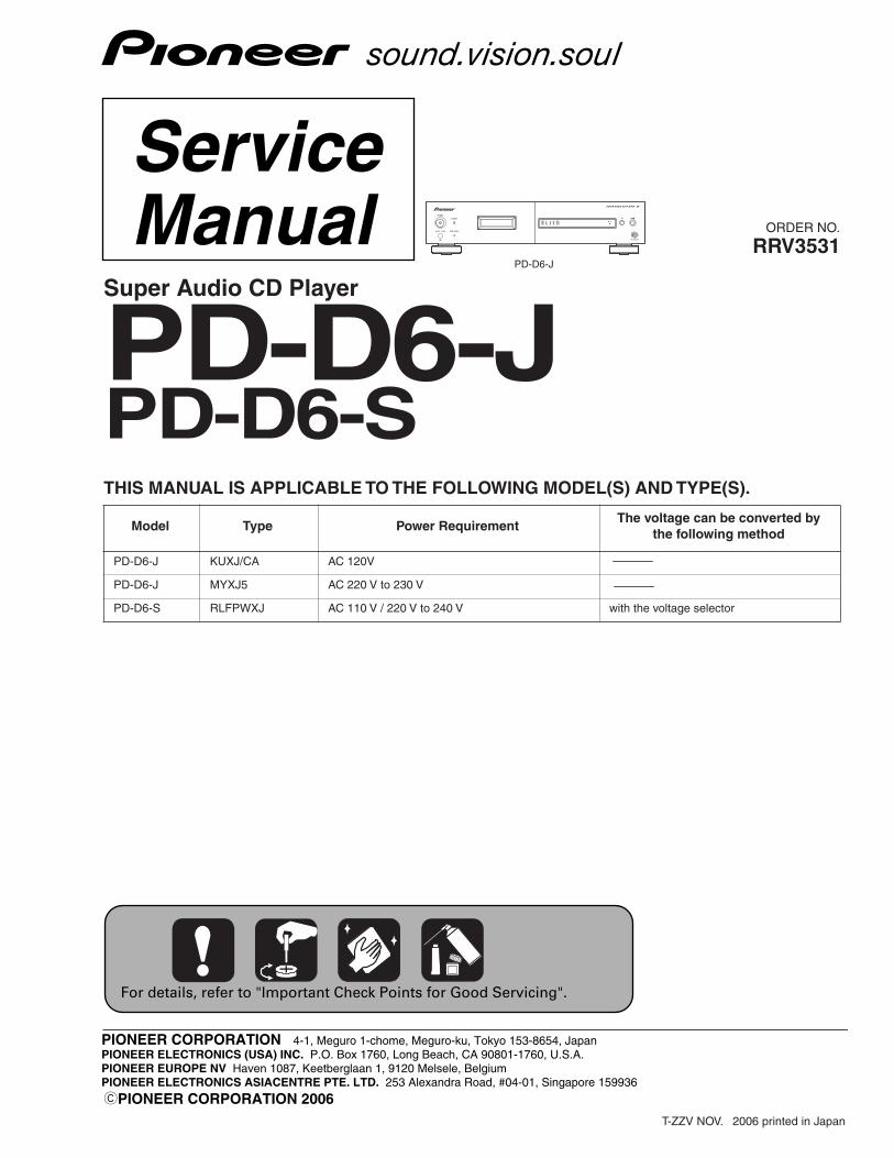
ORDER NO.
RRV3531
Super Audio CD Player
PD-D6-JPD-D6-STHIS MANUAL IS APPLICABLE TO THE FOLLOWING MODEL(S) AND TYPE(S).
Model Type Power RequirementThe voltage can be converted by
the following method
PD-D6-J KUXJ/CA AC 120V
PD-D6-J MYXJ5 AC 220 V to 230 V
PD-D6-S RLFPWXJ AC 110 V / 220 V to 240 V with the voltage selector
For details, refer to "Important Check Points for Good Servicing".
T-ZZV NOV. 2006 printed in Japan
C
D
F
A
B
E
1 2 3 4SAFETY INFORMATION
This service manual is intended for qualified service technicians; it is not meant for the casualdo-it-yourselfer. Qualified technicians have the necessary test equipment and tools, and have beentrained to properly and safely repair complex products such as those covered by this manual.Improperly performed repairs can adversely affect the safety and reliability of the product and mayvoid the warranty. If you are not qualified to perform the repair of this product properly and safely, youshould not risk trying to do so and refer the repair to a qualified service technician.
WARNING
This product contains lead in solder and certain electrical parts contain chemicals which are known to the state of California to
cause cancer, bir th defects or other reproductive harm.
Health & Safety Code Section 25249.6 – Proposition 65
NOTICE
(FOR CANADIAN MODEL ONLY)
Fuse symbols (fast operating fuse) and/or (slow operating fuse) on PCB indicate that replacement
parts must be of identical designation.
REMARQUE
(POUR MODÈLE CANADIEN SEULEMENT)
Les symboles de fusible (fusible de type rapide) et/ou (fusible de type lent) sur CCI indiquent que
les pièces de remplacement doivent avoir la même désignation.
ANY MEASUREMENTS NOT WITHIN THELIMITS OUTLINED ABOVE ARE INDICATIVEOF A POTENTIAL SHOCK HAZARD ANDMUST BE CORRECTED BEFORE RETURN-ING THE APPLIANCE TO THE CUSTOMER.
2. PRODUCT SAFETY NOTICEMany electrical and mechanical parts in the appliance
have special safety related character istics. These areoften not evident f rom visual inspect ion nor theprotection afforded by them necessarily can be obtainedby using replacement components rated for voltage,wattage, etc. Replacement par ts which have thesespecial safety character ist ics are identif ied in thisService Manual.
Electr ical components having such features areidentified by marking with a on the schematics andon the parts list in this Service Manual.The use of a substitute replacement component whichdoes not have the same safety characteristics as thePIONEER recommended replacement one, shown in theparts list in this Service Manual, may create shock, fire,or other hazards.
Product Safety is continuously under review and newinstructions are issued from time to time. For the latestinformation, always consult the current PIONEERService Manual. A subscription to, or additional copiesof, PIONEER Service Manual may be obtained at anominal charge from PIONEER.
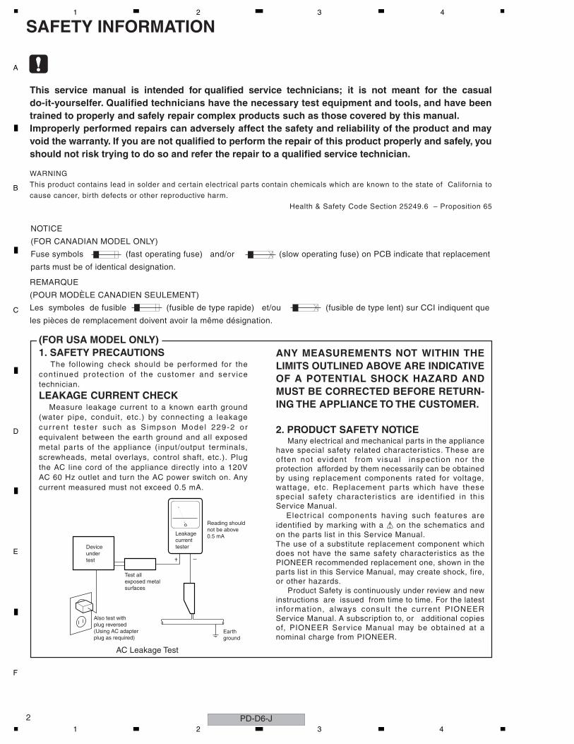
(FOR USA MODEL ONLY)1. SAFETY PRECAUTIONS
The following check should be performed for thecont inued protect ion of the customer and servicetechnician.
LEAKAGE CURRENT CHECKMeasure leakage current to a known ear th ground
(water pipe, conduit, etc.) by connecting a leakagecurrent tes ter such as S impson Model 229-2 orequivalent between the earth ground and all exposedmetal par ts of the appliance (input/output terminals,screwheads, metal overlays, control shaft, etc.). Plugthe AC line cord of the appliance directly into a 120VAC 60 Hz outlet and turn the AC power switch on. Anycurrent measured must not exceed 0.5 mA.
Deviceundertest
Leakagecurrenttester
Earthground
Reading shouldnot be above0.5 mA
Also test withplug reversed(Using AC adapterplug as required)
Test allexposed metalsurfaces
AC Leakage Test
PD-D6-J21 2 3 4
C
D
F
A
B
E
3
5 6 7 8
WARNING !
THE AEL (ACCESSIBLE EMISSION LEVEL) OF THE LASER POWER OUTPUT IS LESS THAN CLASS 1 BUT THE LASER COMPONENT IS CAPABLE OF EMITTING RADIATION EXCEEDING THE LIMIT FOR CLASS 1.A SPECIALLY INSTRUCTED PERSON SHOULD DO SERVICING OPERATION OF THE APPARATUS.
LASER DIODE CHARACTERISTICS
FOR CD : MAXIMUM OUTPUT POWER : 7 mWWAVELENGTH : 780 nm
(FOR DVD : MAXIMUM OUTPUT POWER : 5 mWWAVELENGTH : 650 nm)
Additional Laser Caution
1. Laser Interlock Mechanism• Loading switch (S101 on the LOAB Assy) is used for interlock mechanism of the laser.When this switch turned ON in SW2 (CLOSE) side (OPEN signal is 0V and CLOSE signal is 3.5V), a laser becomes the status which can completely oscillation.Furthermore, the laser completely oscillates in the disc judgment and disc playback.When player is power ON state and laser diode is not completely oscillating, 780nm laser diode is always oscillating by half power.• Laser diode is driving with Q307 (650nm LD) and Q308 (780nm LD) on the DVDM Assy.Therefore, when short-circuit between the emitter and collector of these transistors or the base voltage is supplied for transistors turn on, the laser oscillates. (failure mode)• In the test mode ∗ , there is the mode that the laser oscillates except for the disc judgment and playback. LD ON mode in the test mode oscillates with the laser forcibly.The interlock mechanism mentioned above becomes invalid in this mode.
2. When the cover is open, close viewing through the objective lens with the naked eye will cause exposure to the laser beam.
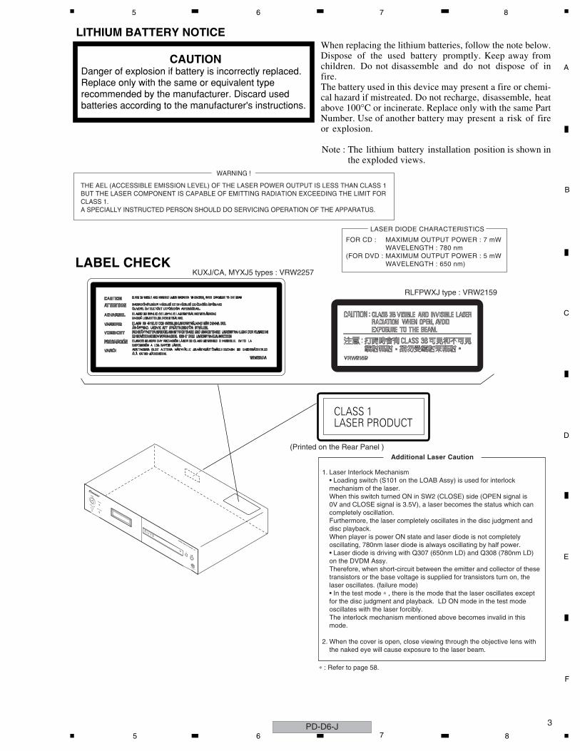
LABEL CHECK
RLFPWXJ type : VRW2159
KUXJ/CA, MYXJ5 types : VRW2257
(Printed on the Rear Panel )
∗ : Refer to page 58.
PD-D6-J5 6 7 8
C
D
F
A
B
E
PD-D6-J4
1 2 3 4
[Important Check Points for Good Servicing]In this manual, procedures that must be performed during repairs are marked with the below symbol.Please be sure to confirm and follow these procedures.
1. Product safety
Please conform to product regulations (such as safety and radiation regulations), and maintain a safe servicing environment by following the safety instructions described in this manual.
1 Use specified parts for repair.
Use genuine parts. Be sure to use important parts for safety.
2 Do not perform modifications without proper instructions.
Please follow the specified safety methods when modification(addition/change of parts) is required due to interferences such as radio/TV interference and foreign noise.
3 Make sure the soldering of repaired locations is properly performed.
When you solder while repairing, please be sure that there are no cold solder and other debris.Soldering should be finished with the proper quantity. (Refer to the example)
4 Make sure the screws are tightly fastened.
Please be sure that all screws are fastened, and that there are no loose screws.
5 Make sure each connectors are correctly inserted.
Please be sure that all connectors are inserted, and that there are no imperfect insertion.
6 Make sure the wiring cables are set to their original state.
Please replace the wiring and cables to the original state after repairs.In addition, be sure that there are no pinched wires, etc.
7 Make sure screws and soldering scraps do not remain inside the product.
Please check that neither solder debris nor screws remain inside the product.
8 There should be no semi-broken wires, scratches, melting, etc. on the coating of the power cord.
Damaged power cords may lead to fire accidents, so please be sure that there are no damages.If you find a damaged power cord, please exchange it with a suitable one.
9 There should be no spark traces or similar marks on the power plug.
When spark traces or similar marks are found on the power supply plug, please check the connection and advise on secure connections and suitable usage. Please exchange the power cord if necessary.
0 Safe environment should be secured during servicing.
When you perform repairs, please pay attention to static electricity, furniture, household articles, etc. in order to prevent injuries. Please pay attention to your surroundings and repair safely.
2. Adjustments
To keep the original performance of the products, optimum adjustments and confirmation of characteristics within specification.Adjustments should be performed in accordance with the procedures/instructions described in this manual.
4. Cleaning
For parts that require cleaning, such as optical pickups, tape deck heads, lenses and mirrors used in projection monitors, proper cleaning should be performed to restore their performances.
3. Lubricants, Glues, and Replacement parts
Use grease and adhesives that are equal to the specified substance. Make sure the proper amount is applied.
5. Shipping mode and Shipping screws
To protect products from damages or failures during transit, the shipping mode should be set or the shipping screws should be installed before shipment. Please be sure to follow this method especially if it is specified in this manual.
1 2 3 4
C
D
F
A
B
E
5
5 6 7 8
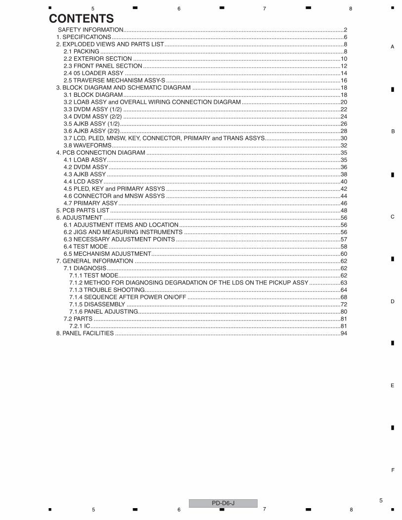
CONTENTS SAFETY INFORMATION......................................................................................................................................21. SPECIFICATIONS.............................................................................................................................................62. EXPLODED VIEWS AND PARTS LIST.............................................................................................................8
2.1 PACKING ....................................................................................................................................................82.2 EXTERIOR SECTION ..............................................................................................................................102.3 FRONT PANEL SECTION ........................................................................................................................122.4 05 LOADER ASSY ...................................................................................................................................142.5 TRAVERSE MECHANISM ASSY-S ..........................................................................................................16
3. BLOCK DIAGRAM AND SCHEMATIC DIAGRAM ..........................................................................................183.1 BLOCK DIAGRAM....................................................................................................................................183.2 LOAB ASSY and OVERALL WIRING CONNECTION DIAGRAM ............................................................203.3 DVDM ASSY (1/2) ....................................................................................................................................223.4 DVDM ASSY (2/2) ....................................................................................................................................243.5 AJKB ASSY (1/2)......................................................................................................................................263.6 AJKB ASSY (2/2)......................................................................................................................................283.7 LCD, PLED, MNSW, KEY, CONNECTOR, PRIMARY and TRANS ASSYS..............................................303.8 WAVEFORMS...........................................................................................................................................32
4. PCB CONNECTION DIAGRAM ......................................................................................................................354.1 LOAB ASSY..............................................................................................................................................354.2 DVDM ASSY.............................................................................................................................................364.3 AJKB ASSY ..............................................................................................................................................384.4 LCD ASSY................................................................................................................................................404.5 PLED, KEY and PRIMARY ASSYS ..........................................................................................................424.6 CONNECTOR and MNSW ASSYS ..........................................................................................................444.7 PRIMARY ASSY.......................................................................................................................................46
5. PCB PARTS LIST ............................................................................................................................................486. ADJUSTMENT ................................................................................................................................................56
6.1 ADJUSTMENT ITEMS AND LOCATION..................................................................................................566.2 JIGS AND MEASURING INSTRUMENTS ...............................................................................................566.3 NECESSARY ADJUSTMENT POINTS ....................................................................................................576.4 TEST MODE.............................................................................................................................................586.5 MECHANISM ADJUSTMENT...................................................................................................................60
7. GENERAL INFORMATION .............................................................................................................................627.1 DIAGNOSIS..............................................................................................................................................62
7.1.1 TEST MODE.......................................................................................................................................627.1.2 METHOD FOR DIAGNOSING DEGRADATION OF THE LDS ON THE PICKUP ASSY...................637.1.3 TROUBLE SHOOTING.......................................................................................................................647.1.4 SEQUENCE AFTER POWER ON/OFF .............................................................................................687.1.5 DISASSEMBLY ..................................................................................................................................727.1.6 PANEL ADJUSTING...........................................................................................................................80
7.2 PARTS ......................................................................................................................................................817.2.1 IC........................................................................................................................................................81
8. PANEL FACILITIES .........................................................................................................................................94
PD-D6-J5 6 7 8
C
D
F
A
B
E
PD-D6-J6
1 2 3 4
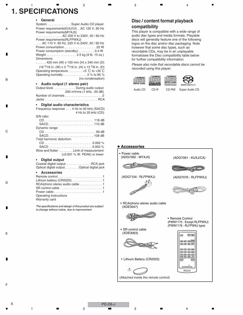
1. SPECIFICATIONSDisc / content format playback compatibilityThis player is compatible with a wide range of audio disc types and media formats. Playable discs will generally feature one of the following logos on the disc and/or disc packaging. Note however that some disc types, such as recordable CDs, may be in an unplayable formatósee the Disc compatibility table below for further compatibility information.
Please also note that recordable discs cannot be recorded using this player.
Audio CD CD-R CD-RW Super Audio CD
• GeneralSystem. . . . . . . . . . . . . . Super Audio CD playerPower requirements(KUXJ/CA) . .AC 120 V, 60 HzPower requirements(MYXJ5) . . . . . . . . . . . . . . .AC 220 V to 230V, 50 / 60 HzPower requirements(RLFPWXJ) . . . AC 110 V, 60 Hz, 220 V to 240V, 50 / 60 HzPower consumption. . . . . . . . . . . . . . . . . . .22 WPower consumption (standby) . . . . . . . . . 0.4 WWeight . . . . . . . . . . . . . . . . . 4.5 kg (9 lb. 15 oz.)Dimensions. . . . . . 420 mm (W) x 100 mm (H) x 340 mm (D)
(16 9/16 in. (W) x 3 15/16 in. (H) x 13 3/8 in. (D)Operating temperature . . . . . . . . +5 to +35Operating humidity . . . . . . . . . . . . . .5 % to 85 %
(no condensation)
• Audio output (1 stereo pair)Output level. . . . . . . . . . . . . During audio output
200 mVrms (1 kHz, -20 dB)Number of channels . . . . . . . . . . . . . . . . . . . . . 2Jacks . . . . . . . . . . . . . . . . . . . . . . . . . . . . . . RCA
• Digital audio characteristicsFrequency response . . . 4 Hz to 50 kHz (SACD)
4 Hz to 20 kHz (CD)S/N ratio:
CD . . . . . . . . . . . . . . . . . . . . . . . . . . . . 118 dBSACD. . . . . . . . . . . . . . . . . . . . . . . . . . 110 dB
CD . . . . . . . . . . . . . . . . . . . . . . . . . . . . . 99 dBSACD. . . . . . . . . . . . . . . . . . . . . . . . . . 108 dB
Dynamic range:
Total harmonic distortion:CD . . . . . . . . . . . . . . . . . . . . . . . . . . . 0.002 %SACD. . . . . . . . . . . . . . . . . . . . . . . . . 0.003 %
Wow and flutter . . . . . . . . Limit of measurement(±0.001 % W. PEAK) or lower
• Digital outputCoaxial digital output. . . . . . . . . . . . . . .RCA jackOptical digital output. . . . . . . . Optical digital jack
• AccessoriesRemote control . . . . . . . . . . . . . . . . . . . . . . . . . 1Lithium battery (CR2025) . . . . . . . . . . . . . . . . . 1RCA/phono stereo audio cable . . . . . . . . . . . . . 1SR control cable . . . . . . . . . . . . . . . . . . . . . . . . 1Power cable . . . . . . . . . . . . . . . . . . . . . . . . . . . 1Operating Instructions Warranty card
The specifications and design of this product are subject to change without notice, due to improvement.
Accessories
• Power cable (ADG7062 : MYXJ5) (ADG7061 : KUXJ/CA)
(ADG7076 : RLFPWXJ)(ADG7104 : RLFPWXJ)
• RCA/phono stereo audio cable (XDE3047)
• SR control cable (XDE3063)
• Remote Control (PWW1175 : Except RLFPWXJ) (PWW1176 : RLFPWXJ type)
• Lithium Battery (CR2025)
(Attached inside the remote control)
>
1 2 3 4

C
D
F
A
B
E
7
5 6 7 8
PD-D6-J5 6 7 8
C
D
F
A
B
E
PD-D6-J8
1 2 3 4
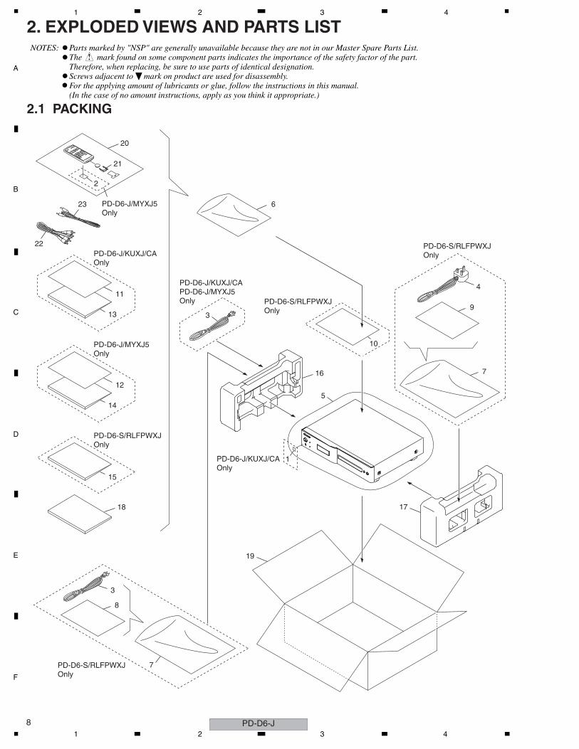
2. EXPLODED VIEWS AND PARTS LIST
2.1 PACKING
Parts marked by "NSP" are generally unavailable because they are not in our Master Spare Parts List.The mark found on some component parts indicates the importance of the safety factor of the part.Therefore, when replacing, be sure to use parts of identical designation.Screws adjacent to mark on product are used for disassembly. For the applying amount of lubricants or glue, follow the instructions in this manual.(In the case of no amount instructions, apply as you think it appropriate.)
NOTES:
PD-D6-J/MYXJ5Only
PD-D6-J/KUXJ/CAPD-D6-J/MYXJ5Only
PD-D6-J/MYXJ5Only
PD-D6-S/RLFPWXJOnly
PD-D6-S/RLFPWXJOnly
PD-D6-S/RLFPWXJOnly
20
6
18
16
17
19
8
11
13
10
12
14
15
3
9
7
7
4
3
5
1
23
22
21
2
PD-D6-J/KUXJ/CAOnly
PD-D6-J/KUXJ/CAOnly
PD-D6-S/RLFPWXJOnly
1 2 3 4
C
D
F
A
B
E
9
5 6 7 8
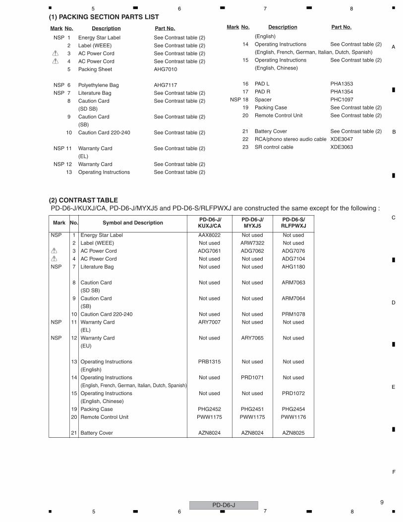
(1) PACKING SECTION PARTS LIST
(2) CONTRAST TABLE PD-D6-J/KUXJ/CA, PD-D6-J/MYXJ5 and PD-D6-S/RLFPWXJ are constructed the same except for the following :
Mark No. Description Part No.
NSP 1 Energy Star Label See Contrast table (2)
2 Label (WEEE) See Contrast table (2)
> 3 AC Power Cord See Contrast table (2)
> 4 AC Power Cord See Contrast table (2)
5 Packing Sheet AHG7010
NSP 6 Polyethylene Bag AHG7117
NSP 7 Literature Bag See Contrast table (2)
8 Caution Card See Contrast table (2)
(SD SB)
9 Caution Card See Contrast table (2)
(SB)
10 Caution Card 220-240 See Contrast table (2)
NSP 11 Warranty Card See Contrast table (2)
(EL)
NSP 12 Warranty Card See Contrast table (2)
13 Operating Instructions See Contrast table (2)
(English)
14 Operating Instructions See Contrast table (2)
(English, French, German, Italian, Dutch, Spanish)
15 Operating Instructions See Contrast table (2)
(English, Chinese)
16 PAD L PHA1353
17 PAD R PHA1354
NSP 18 Spacer PHC1097
19 Packing Case See Contrast table (2)
20 Remote Control Unit See Contrast table (2)
21 Battery Cover See Contrast table (2)
22 RCA/phono stereo audio cable XDE3047
23 SR control cable XDE3063
Mark No. Description Part No.
Mark No. Symbol and Description PD-D6-J/ KUXJ/CA
PD-D6-J/ MYXJ5
PD-D6-S/RLFPWXJ
NSP 1 Energy Star Label AAX8022 Not used Not used
2 Label (WEEE) Not used ARW7322 Not used
> 3 AC Power Cord ADG7061 ADG7062 ADG7076
> 4 AC Power Cord Not used Not used ADG7104
NSP 7 Literature Bag Not used Not used AHG1180
8 Caution Card Not used Not used ARM7063
(SD SB)
9 Caution Card Not used Not used ARM7064
(SB)
10 Caution Card 220-240 Not used Not used PRM1078
NSP 11 Warranty Card ARY7007 Not used Not used
(EL)
NSP 12 Warranty Card Not used ARY7065 Not used
(EU)
13 Operating Instructions PRB1315 Not used Not used
(English)
14 Operating Instructions Not used PRD1071 Not used
(English, French, German, Italian, Dutch, Spanish)
15 Operating Instructions Not used Not used PRD1072
(English, Chinese)
19 Packing Case PHG2452 PHG2451 PHG2454
20 Remote Control Unit PWW1175 PWW1175 PWW1176
21 Battery Cover AZN8024 AZN8024 AZN8025
PD-D6-J5 6 7 8
C
D
F
A
B
E
PD-D6-J10
1 2 3 4
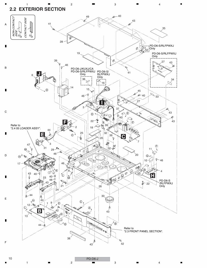
2.2 EXTERIOR SECTION
CO
NT
AC
T S
IDE
NO
N-C
ON
TA
CT
S
IDE
PD-D6-S/RLFPWXJ Only
PD-D6-S/RLFPWXJ Only
PD-D6-S/RLFPWXJ Only
PD-D6-S/RLFPWXJ Only
PD-D6-J/KUXJ/CAPD-D6-S/RLFPWXJ
Only
A
A
B
B
E
E
F
G
F
C
C
D
D
41
46
46
44
3
3147
8
17
29
46
46
46
21
4040
44
12
13
1 9
4843
43
42 43
30
2622
4
4610
50
11
7
20
32
25
20
18
22
32
43
43
34
27
45
40
39
37
40
39
42
23
24
44
44
38
43
5
14
39
6
2
19
36
15
16
41
5251
49
28
40
43
43
35
27
J
I
F
E
B
H
C
G
H
H
IJ
I J
K
K
L
L
M
M
Refer to"2.3 FRONT PANEL SECTION".
Refer to"2.4 05 LOADER ASSY".
33
1 2 3 4
C
D
F
A
B
E
11
5 6 7 8
(1) EXTERIOR SECTION PARTS LIST
(2) CONTRAST TABLE PD-D6-J/KUXJ/CA, PD-D6-J/MYXJ5 and PD-D6-S/RLFPWXJ are constructed the same except for the following :
Mark No. Description Part No.
1 DVDM ASSY AWM8069
2 MNSW ASSY AWX8794
3 PLED ASSY AWX8795
4 CONNECTOR ASSY AWX8796
5 PRIMARY ASSY See Contrast table (2)
6 TRANS ASSY See Contrast table (2)
7 AJKB ASSY AWM8075
NSP 8 Cord With Plug ADH7022
9 17P FFC PDD1230
10 29P FFC PDD1231
11 15P FFC PDD1232
12 Connector ASSY PG05KK-E07
NSP 13 Cord With Plug DE005VF0
> 14 Power Transfomer See Contrast table (2)
> 15 Fuse 1 See Contrast table (2)
> 16 Fuse 2 See Contrast table (2)
NSP 17 05 LOADER ASSY VWT1230
18 Shield Cusion AEB7372
19 SR Sheet L PEB1319
20 SR Sheet S PEB1320
NSP 21 Flatcable Clamp AEC7376
22 PCB Spacer KGPS-12S AEC7517
23 Adapter05 L ANW7282
24 Adapter05 R ANW7283
25 Side Clamp DEC2007
NSP 26 Chassis PNA2602
27 Rear Panel See Contrast table (2)
28 Bonnet See Contrast table (2)
29 PCB Holder PNW2029
30 Insulater See Contrast table (2)
31 Power Button ASSY See Contrast table (2)
NSP 32 PCB Angle 989 VNE2409
NSP 33 Label VRW1629
NSP 34 SISIR Label See Contrast table (2)
35 Caution Label See Contrast table (2)
36 Fuse Label See Contrast table (2)
NSP 37 Binder ZCA-BK1
38 Tray Panel See Contrast table (2)
39 Screw ABA1192
40 Screw ABA7017
41 Deco. Screw 4X10 See Contrast table (2)
42 Screw BBT30P080FNI
43 Screw BBZ30P080FCC
44 Screw BPZ30P080FTC
45 Screw CBZ30P080FCC
46 Screw IBZ30P060FCC
47 Screw VBA1094
48 Washer PEC1046
49 Washer WG40FCC
50 Spacer See Contrast table (2)
51 Washer See Contrast table (2)
52 Washer See Contrast table (2)
Mark No. Description Part No.
Mark No. Symbol and Description PD-D6-J/ KUXJ/CA
PD-D6-J/ MYXJ5
PD-D6-S/RLFPWXJ
5 PRIMARY ASSY AWX8800 AWX8799 AWX8801
6 TRANS ASSY AWX8802 AWX8802 AWX8797
> 14 Power Transfomer PTT1369 PTT1368 PTT1370
> 15 Fuse 1 REK1058 REK1134 REK1023
(1.25 A/ 250 V) (T500 mA/ 250 V) (T1.25 A / 250 V)
> 16 Fuse 2 (T500 mA / 250 V) Not used Not used REK1134
27 Rear Panel PNA2606 PNA2605 PNA2607
28 Bonnet PNA2610 PNA2610 PNA2603
30 Insulater PNW2766 AMR7198 PNW2766
31 Power Button ASSY PXA1644 PXA1644 VXA2724
NSP 34 SISIR Label Not used Not used PRW1601
35 Caution Label VRW2257 VRW2257 VRW2159
36 Fuse Label XAX3161 Not used XAX3161
NSP 38 Tray Panel PNW3048 PNW3051 PNW3044
41 Deco. Screw 4X10 ABA7136 ABA7136 ABA7135
50 Spacer Not used Not used PEC1049
51 Washer Not used Not used PEC1048
52 Washer Not used Not used WB40FTC
PD-D6-J5 6 7 8
C
D
F
A
B
E
PD-D6-J12
1 2 3 4
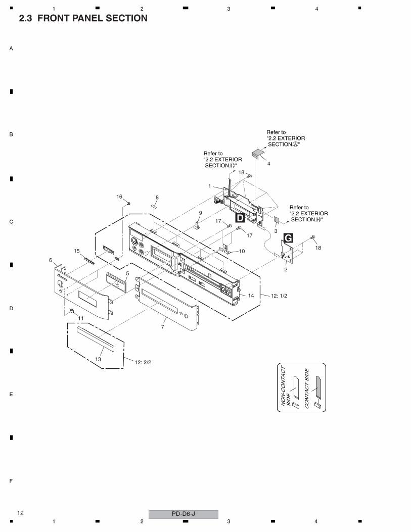
2.3 FRONT PANEL SECTION
CO
NT
AC
T S
IDE
NO
N-C
ON
TA
CT
S
IDE
1
4
3
2
18
18
17
10
17
9
8
5
16
15
11
6
D
G
Refer to"2.2 EXTERIOR SECTION. "A
Refer to"2.2 EXTERIOR SECTION. "B
Refer to"2.2 EXTERIOR SECTION. "C
12: 1/2
13
7
14
12: 2/2
1 2 3 4
C
D
F
A
B
E
13
5 6 7 8
(1) FRONT PANEL SECTION PARTS LIST
(2) CONTRAST TABLE PD-D6-J/KUXJ/CA, PD-D6-J/MYXJ5 and PD-D6-S/RLFPWXJ are constructed the same except for the following :
Mark No. Description Part No.
1 LCD ASSY AWX8790
2 KEY ASSY AWX8792
3 15P FFC PDD1229
4 17P FFC PDD1233
5 D.Window PAM1866
NSP 6 AL Panel L See Contrast table (2)
NSP 7 AL Panel R See Contrast table (2)
8 Himelon Sheet PEB1321
9 Earth Plate PNB1662
10 Earth Plate C PNB1664
11 Lens See Contrast table (2)
NSP 12 Panel ASSY See Contrast table (2)
13 Tray Panel See Contrast table (2)
14 Panel Stay See Contrast table (2)
15 Pioneer Badge VAM1124
NSP 16 LED Lens VNK5073
17 Screw BBZ30P080FCC
18 Screw BPZ30P080FTC
Mark No. Description Part No.
Mark No. Symbol and Description PD-D6-J/ KUXJ/CA
PD-D6-J/ MYXJ5
PD-D6-S/RLFPWXJ
NSP 6 AL Panel L PAN1389 PAN1389 PAN1385
NSP 7 AL Panel R PAN1390 PAN1391 PAN1386
11 Lens PNW3047 PNW3047 AAK7586
NSP 12 Panel ASSY PXA1645 PXA1646 PXA1647
13 Tray Panel PNW3048 PNW3051 PNW3044
14 Panel Stay PNW3049 PNW3049 PNW3043
PD-D6-J5 6 7 8
C
D
F
A
B
E
PD-D6-J14
1 2 3 4
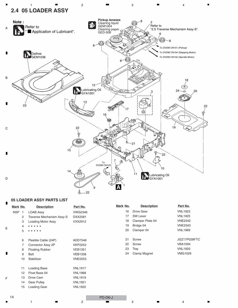
2.4 05 LOADER ASSY
05 LOADER ASSY PARTS LIST
A
A
To DVDM CN101 (Pickup)
To DVDM CN104 (Stepping Motor)
To DVDM CN102 (Spindle Motor)
ToDVDM CN103
2Refer to "2.5 Traverse Mechanism Assy-S".
12
2313
17
21
16
22
15
14
22
22
22
20
19
91
7
10
11
6
8
8
8
8
18
24
A
Lubricating OilGYA1001
DaifreeGEM1036
Refer to" Application of Lubricant".
Note :
Lubricating OilGYA1001 3
Pickup leneses Cleaning liquid GEM1004 Cleaning paper GED-008
Mark No. Description Part No.
NSP 1 LOAB Assy VWG2346
2 Traverse Mechanism Assy-S DXX2581
3 Loading Motor Assy VXX2912
4 • • • • •
5 • • • • •
6 Flexible Cable (24P) ADD7546
7 Connector Assy 2P VKP2253
8 Floating Rubber VEB1351
9 Belt VEB1358
10 Stabilizer VNE2253
11 Loading Base VNL1917
12 Float Base 04 VNL1968
13 Drive Cam VNL1919
14 Gear Pulley VNL1921
15 Loading Gear VNL1922
16 Drive Gear VNL1923
17 SW Lever VNL1925
18 Clamper Plate 04 VNE2342
19 Bridge 04 VNE2343
20 Clamper 04 VNL1969
21 Screw JGZ17P028FTC
22 Screw VBA1094
23 Tray VNL1920
24 Clamp Magnet VMG1029
Mark No. Description Part No.
1 2 3 4
C
D
F
A
B
E
15
5 6 7 8
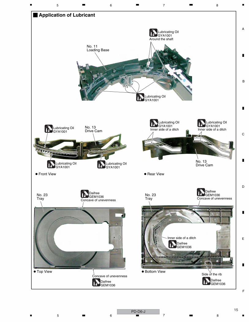
Application of Lubricant
Lubricating OilGYA1001
Around the shaft
No. 11 Loading Base
No. 13 Drive Cam
No. 13 Drive Cam
No. 23 Tray
No. 23 Tray
Front View Rear View
DaifreeGEM1036
Inner side of a ditch
Concave of unevennessTop View Bottom View
DaifreeGEM1036
DaifreeGEM1036
Side of the rib
Concave of unevenness
DaifreeGEM1036 Concave of unevenness
DaifreeGEM1036
Inner side of a ditch
Lubricating OilGYA1001
Inner side of a ditch
Lubricating OilGYA1001
Lubricating OilGYA1001
Lubricating OilGYA1001
Lubricating OilGYA1001
Lubricating OilGYA1001
PD-D6-J5 6 7 8
C
D
F
A
B
E
PD-D6-J16
1 2 3 4
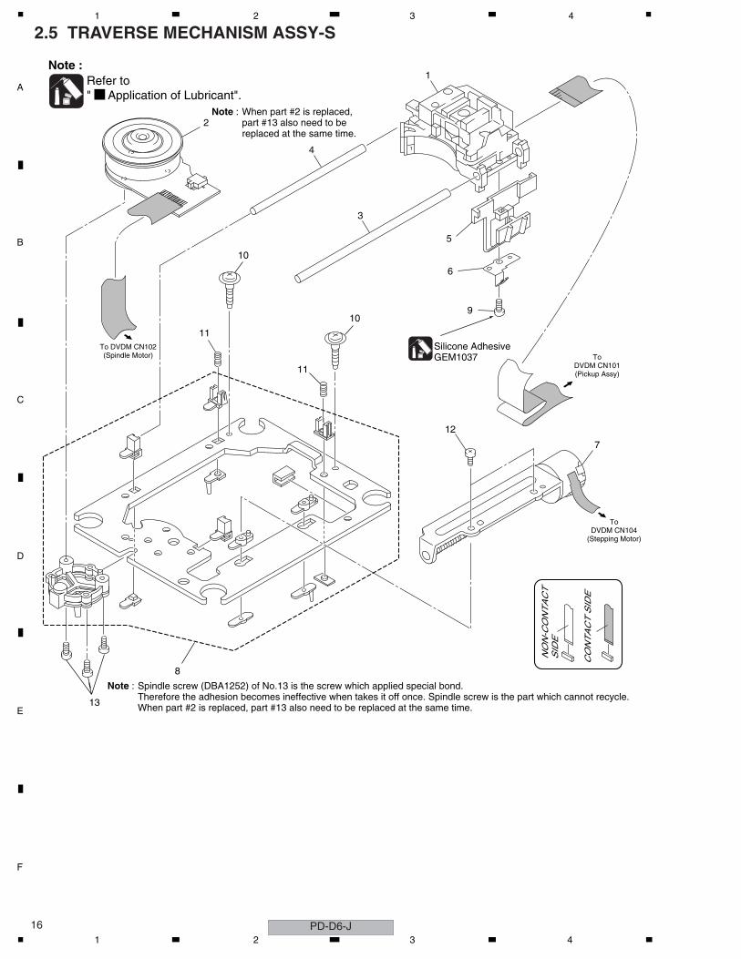
2.5 TRAVERSE MECHANISM ASSY-S
ToDVDM CN101(Pickup Assy)
ToDVDM CN104
(Stepping Motor)
To DVDM CN102(Spindle Motor)
CO
NT
AC
T S
IDE
NO
N-C
ON
TA
CT
S
IDE
13
10
10
11
11
12
2
4
1
3
6
9
5
7
Silicone AdhesiveGEM1037
Refer to" Application of Lubricant".
Note :
Note : When part #2 is replaced, part #13 also need to be replaced at the same time.
8
Note : Spindle screw (DBA1252) of No.13 is the screw which applied special bond.Therefore the adhesion becomes ineffective when takes it off once. Spindle screw is the part which cannot recycle.When part #2 is replaced, part #13 also need to be replaced at the same time.
1 2 3 4
C
D
F
A
B
E
17
5 6 7 8
TRAVERSE MECHANISM ASSY-S PARTS LIST
Mark No. Description Part No.
> 1 05SD Pickup Assy-s OXX8019
2 Spindle Motor N200 DXM1197
NSP 3 Guide Shaft VK1 DLA1940
NSP 4 Sub Guide Shaft VK1 DLA1941
NSP 5 Joint VK1B DNK4272
NSP 6 Joint Spring VK1 DBK1235
7 Stepping Motor VK1 DXM1201
NSP 8 Mechanism Frame VK1 DNK4160
9 Precision Screw VK1 DBA1209
10 Skew Screw VK1 DBA1211
11 Skew Spring VK1 DBH1516
NSP 12 Stepping Screw DBA1205
13 Spindle Screw VK1(for Service) DBA1252
PD-D6-J5 6 7 8
C
D
F
A
B
E
PD-D6-J18
1 2 3 4
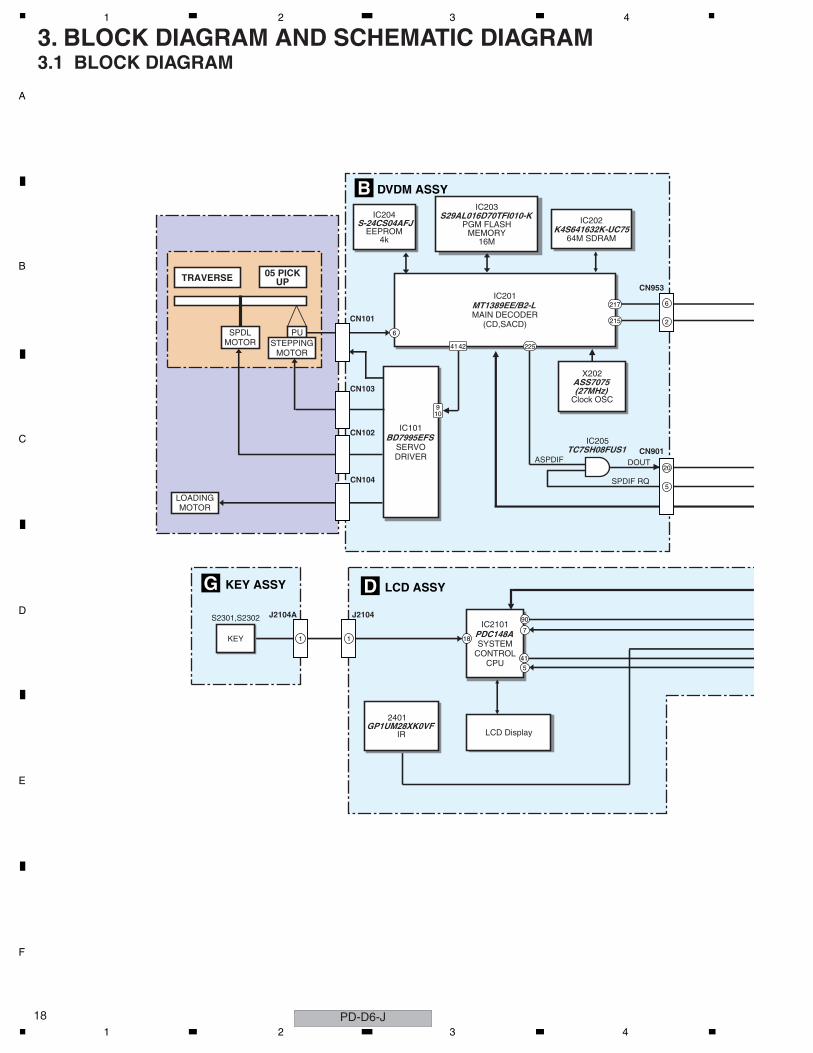
3. BLOCK DIAGRAM AND SCHEMATIC DIAGRAM3.1 BLOCK DIAGRAM
MAIN DECODER
IC201
(CD,SACD)
MT1389EE/B2-L
EEPROM
IC204
4k
S-24CS04AFJ
LOADINGMOTOR
SPDLMOTOR
PUSTEPPING
MOTOR
TRAVERSE 05 PICKUP
SERVO
IC101
DRIVER
BD7995EFS IC205TC7SH08FUS1
Clock OSC
X202ASS7075(27MHz)
ASPDIF DOUT
SPDIF RQ
CN101
CN104
CN103
CN102
DVDM ASSYB
LCD ASSYD
IC203
PGM FLASHMEMORY
16M
S29AL016D70TFI010-K
64M SDRAM
IC202K4S641632K-UC75
CN953
2
CN901
5
20
90
7
5
J2104A J2104
KEY ASSYG
SYSTEM
IC2101
CONTROLCPU
PDC148A
IR
2401GP1UM28XK0VF
LCD Display
11KEY
S2301,S2302
6217
215
225
6
18
41
41 42
910
1 2 3 4
C
D
F
A
B
E
19
5 6 7 8
PLED ASSYE
SR-IN
SR-OUT
L
R
LPFL/R (PCM)I/V
L/R (DSD)
DOUT DOUT DOUT
SPDIF_RQ
SRIN
SROUT
SRIN
SROUT
MCLK
IC1101 IC1102(1/2)
IC1201 IC1102(2/2)
192k,24bit,
IC1301
DAC Lch
PCM1738EG-3
192k,24bit,
IC1401
DAC Rch
PCM1738EG-3
AJKB ASSYC
CONNECTOR ASSYH
TRANS ASSYJ
PRIMARY ASSYI
CN1501
CN2701CN2702
26
14
PCM/DSD
IC1601TC74VHC157FTS1
SEL Lch 1617
2526
14
PCM/DSD
IC1602TC74VHC157FTS1
SEL Rch
1617
2526
AQE
IC1501PD0274A
JA1101
JA1201
JA1752
JA1751
OPTICAL OUTJA1702
COAXIAL OUTJA1701
25
10 3
CN1851
CN1503
J51CN13
J11CN2501
J12
J13
13
CN2703
CN1801
J52
5
CN2106
11
J2102
CN2503
CN2105
2
1
CN1502
1
2
AC IN
LED
2
CN2502
J2601
PLE
D
MNSW ASSYF
2
2
Voltage SelectorSW11
PD-D6-S ONLY
6 1 24
6
5
6
5
7
7
5
5
16 16SYSPOW SYSPOW
1 1
22
11
1
2
2
T51
8.3V
10.8V
3.3V
5V
5.8V
6.5V POWERSUPPLY
PD-D6-J5 6 7 8
C
D
F
A
B
E
PD-D6-J20
1 2 3 4
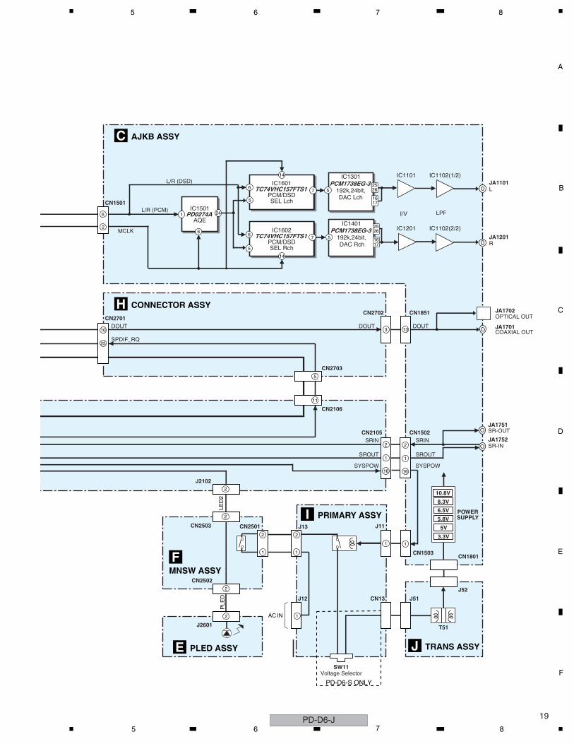
3.2 LOAB ASSY and OVERALL WIRING CONNECTION DIAGRAM
E PLED ASSY(AWX8795)
F MNSW ASSY(AWX8794)
I PRIMARY ASSY(PD-D6-J/KUXJ:AWX8800)(PD-D6-J/MYXJ5:AWX8799)(PD-D6-S/RLFPWXJ:AWX8801)
JTRANS ASSY(PD-D6-J:AWX8802)(PD-D6-S:AWX8797)
W138W137
PF02PG-C07
J2601 2 1
VOUTV+5UGNDD
IR
W136
2P
LED
S2B-PH-K-S
CN2502
L=75
mm
1V
+5U
CN25031234 GNDD
LED2
V+5U
MSDCT
L=120mm
321
1 2
PF04PG-C12J2102
4
3 4
CN2101
76
52492-0720
5
CN21059607S-17F
1 2 543 876
IRO
UT
SR
IN
XD
FD
TG
ND
DG
ND
D
XD
FC
SX
DF
CLK
XD
FR
ST
11109 141312 171615
XS
YS
MU
TE
V+
56S
TG
ND
D
GN
DU
GN
DU
V+
58U
XD
AC
RS
TS
YS
PO
WA
C
B4B-PH-K-S
WE
N/D
IW
D0
Power SW)(Mechanical S2301
VK
N20
24
CN
2501
1 2
Transformer PKP1017
Power
PKP101812
J51
HO
T(V
H)
NE
UT
RA
L
1 2B2P3-VH
CN13
PKP1015 J13
2
1 RY11
PKP1014 FU1J12
2
1
WC
LKR
ST
VC
CV
SS
N.C
.
PD
D12
33
21
FF
CP
=1.
25m
mL=
300m
m
3 4 5 6 7 8 9 10 11
SPINDLE MOTOR
124 312
STEPPING MOTOR
21 43
12
43
MECHA2MECHA1DIGITAL2DIGITAL1
J52
U+
FF
CP
=1.0m
m
V+
5S12 11
V-
U-
V+
W-
HB
W+ VU W
10 9 8 7 6 5 24 3
7
AUDIO2AUDIO16
AUDIO CT
5AKN7031
CN102
INS
IDE
FF
CP
=1.0m
m
ST
1-(A)
ST
1+(A
)S
T2+
(B)
ST
2-(B)
1 34 2 1
FO
CS
RT
NF
OC
S D
RV
TR
KG
RT
NT
RK
G D
RV
24 23 22 21
RKN1045
CN103
SR
OU
T
XD
FD
TX
DF
CLK
XD
FC
SX
DF
RS
T
SR
ING
ND
DG
ND
D
21 543 876
DIGITAL1DIGITAL2
MECHA2MECHA1
432
5
1
XS
YS
MU
TE
V+
56S
T
V+
58U
SY
SP
OW
XD
AC
RS
T
GN
DD
GN
DU
GN
DU
AC
11109 141312 171615 CKS3382CN1502
AC INLET W129W124
AC CORD
4
AUDIO1AUDIO2
AUDIO CT
GNDU
7
4
6
B7B-EHCN1801
PF04PG-C07
123
J11 L=75mm
V+56STAC
SYSPOW
B4B-PH-K-SCN1503
321
RK
N10
04JA
1751
SR
-OU
T
RK
N10
04JA
1752
SR
-IN
3 2 PKP10161
VL
B3P5-VH1 2 3
SW11
HIGHAKX1033
LOW
RD : PTT1370
WY : PTT1368KU : PTT1369PD-D6-J
PD-D6-S
PD-D6-J ONLY
PD-D6-S ONLY
PD-D6-J ONLY
PD-D6-J ONLY PD-D6-S
ONLY
RD : ADG7076
WY : ADG7062
ADG7104
KU : ADG7061
1 2 3 4
C
D
F
A
B
E
21
5 6 7 8
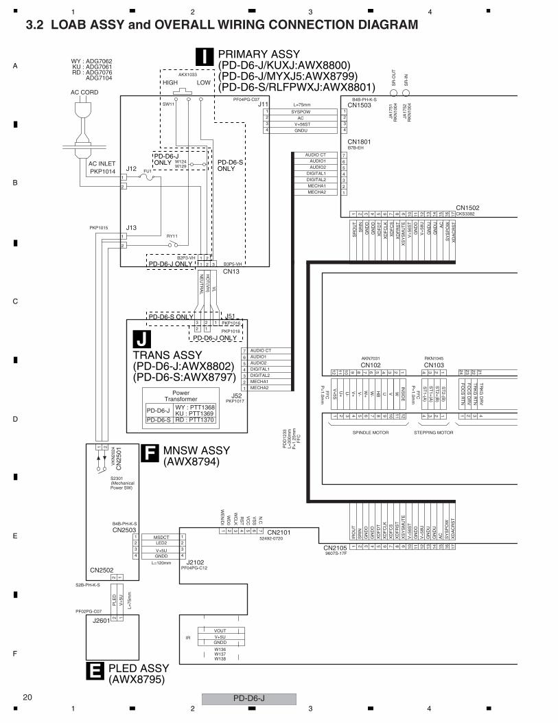
CAJKB ASSY(AWM8075)
BDVDM ASSY(AWM8069)
H CONNECTOR ASSY(AWX8796)
MECHA ASSY(AWM7967)
D LCD ASSY(AWX8790)
G KEY ASSY(AWX8792)
D20PYY0320EJ2104
21 KEY1
VE+53 GNDD
J2104A
21
3
L=200mmP=2.0mm
98765 14 1813121110 171615
PICKUP ASSY
2322212019 24 34 2 15
PG
05KK
-E07
GN
DD
VS
HF
LD(650)P
DLD
(780)
20 19 1618 17
VR
CO
MV
R780
GN
DD
VR
650A B SWRF C
15 14 13 12 11 10 9 8 7
VC
C
GN
DD
VR
EF
AD
D7546
P=
0.5mm
L=220m
m
FF
C
ED F
46 5 123
SW
2G
ND
D
1
SW
15
L=75m
m
LOA
D-
LOA
D+
24 3
FFC
PDD1231L=100mmP=1.0mm
CN101CKS5045
292827262524
AKM1291CN104 V+12A 1
V+9DV+9D
32
V+6R5VV+6R5V 5
4
201918
212223
GNDMGNDMGNDD 8
76
DOUTGNDD
109
GNDDGNDD
1211
GN
DD
1 3 42 5 6 7 8 9 10 11
MC
LK(22M
)G
ND
DLR
CK
DA
TA
0G
ND
D
GN
DD
GN
DD
DA
TA
1
GN
DD
BC
K
1 3 42 5 6 7 8 9 10 1112 13 14 15 16 17
CKS3885CN953
XD
AC
CS
1X
DA
CC
KX
DA
CD
T
XP
CM
/DS
DG
ND
DX
DA
CC
S2
PD
D1230
P=
1.0mm
L=120m
m
FF
C
171615
1314
1211
DVDPOWERXDVDRST 14
13
XREADYSCLK 16
15
SDATAMDATA 18
17
12 13 14 15 16 17 VKN1248
10 GNDDGNDD9
ACK
212019
78
DVDMUTEVDET
2322
65 SPDIF_RQ
TRKUP2524
CN1501
CN
901V
KN
1321
43 TRIN
TRGAIN2726
VK
N1205
CVBSTROUT
12
2928
SP
DIF
P_R
Q
14 13 12 1115 10 9 8 7 6 5 24 3 1
CKS3829CN2106
TR
INV
DE
T
L=285m
mP
=1.0m
mF
FC
TR
OU
TT
RG
AIN
PD
D1229
54321
GN
DD
GN
DD
MD
AT
A
SD
AT
AS
CLK
AC
K
XR
EA
DY
XD
VD
RS
T
DV
DP
OW
ER
86 7 119 10 141312
GN
DD
VKN119115
CN2703
CN2704B2P-SHF-1AA
CV
BS
GN
DD
21
CKS3380
CN
2701
(TO
TX
147L
)
PK
B10
41JA
1101
VK
S10
02
VK
B10
97JA
1701
PK
B10
42JA
1201
JA17
02
Lch
OU
T
Rch
OU
T
OP
T-O
UT
CO
AX
-OU
T
GN
DD
GN
DD
FF
CP
=1.25m
m
DV
DM
UT
E
1 2
PD
D1232
3 4 5
GN
DD
DO
UT
L=125m
m
6 7 8 9 10 11 1412 13
GN
DM
GN
DM
GN
DD
V+
6R5V
V+
6R5V
GN
DD
GN
DD
V+
9DV
+9D
15V
+12A
CN2702
1415 111213 8910 7 56 34 2 1 CKS3380CN1851
B 1/2, B 2/2
C 1/2, C 2/2
V+
3D
SW
2
LOA
D+
LOA
D-
SW
1
S5B
-PH
-K-S
CN
601
CN
602
LOADING MOTOR ASSY : VXX2912
LOAB ASSY(VWG2346)A
12
÷ When ordering service parts, be sure to refer to "EXPLODED VIEWS and PARTS LIST" or "PCB PARTS LIST".
÷ The > mark found on some component parts indicates the importance of the safety factor of the part. Therefore, when replacing, be sure to use parts of identical designation.
÷ : The power supply is shown with the marked box.
PD-D6-J5 6 7 8
C
D
F
A
B
E
PD-D6-J22
1 2 3 4
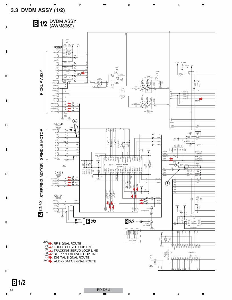
3.3 DVDM ASSY (1/2)
DVDM ASSY(AWM8069)
TROUT
TRIN
LIMIT
TRGAIN
2 31 86 74 5
47 4648 45 44 42 4143
12
9
1110 1413 15 16 17
40 3839 37 36 3435 33 32
5
3
4
1
2
4
3
2
1
1 32 6 8754
12
11
10
8
9
44 4243 3839 374041
6
7
4
5
2
3
1
24
22
23
21
20
18
19
16
17
15
14 5
2
1
5
6
7
4
3
2
8 1
10
9
11 12 14 15 1613 18 21201917 22
BE
C
3335 3436 3132 30 29 2627 242528 23
13
12
11
10
9
8
4 3
6
7
5
4
2
3
1
R284
R285
IC20
3
C28
9
C29
6
R28
2
CN104
C15
3
C15
2
C15
1
C10
3
CN103 R13
2
R13
3
R13
1
R13
6
R13
4
C13
3
R13
5 C10
1
IC101
C140
C102
C14
1
C14
2
C14
3
CN102
R302
R318
Q102
R14
2
R21
9
R21
8
R208
Q101
R141
R15
2
R15
4
R15
1
R15
3C
104
C121
IC204
C290
C22
1R216
C219
C217
C13
1
C13
2
R214
Q201
C14
4
C16
1
C20
9
C21
2
C14
5
C14
6
C21
0
C20
8
C21
1
R210
R211
R213R215
R212
C218C216
R206
R205
R202
R204
R201
C206 C214
C204
C205
C213
C203 C215
Q307
Q307
R32
5
R32
2
C30
9
L308
L309Q308
C31
0
C345
C347
C344
C346
C343
C207
C20
1
C20
2
R371R303
R372
R373
R374
Q305R315
R313
R31
4
Q304
R375
C371
C373
C372
CN101C374
R301
R32
1
R32
6
C32
0
R31
0Q308
R200
R207
PW
R#
PC
E#
A16
A15
A14
A10
A13
A12
A9
A11
ALE
IOC
E#
IOW
R#
UP
3_1
INT
0#
UR
D#
UW
R#
A17
AD
6
AD
7
A0
PW
R#
A20
A19
A18
AD
5
AD
3
AD
2
AD
4
TROUT
TRIN
LOAD+
LOAD-
LOA
D+
LOA
D-
F-
F+
T+
T-
ST2+
ST1-
ST1+
ST2-
HU-
HU+
HV+
HV-
W
V
HW+
HW-
U
HU
+
HW
+
HW
-
HV
-
HV
+
HU
-F+
F-
T+
T-
SDA
SCL
ST
1-
ST
2-S
T2+
ST
1+
TRSO
FOSO
TROPEN
FMSO
PWMOUT1
A4
A7
A6
A18
A3
A19
A8
A2
A5
STBY
ENDM
TROUT
TRIN
FG
FOSO
TRSO
TROPEN
FMSO
PWMOUT1
DMSO
DMSO
ENDM
STBY
FG
U WV
LDO1
F
LDO2
E
MDI1
LDO2
C
RF
B
A
D
LDO1
MDI1
B
A
IOA
RF
C
D
E
F
IOA
10k
GNDD***
S29
AL0
16D
70T
FI0
10-K
V+3D
GNDD
FLA
SH
GNDD
V+3D
1000
p
1
***
S-24CS04AFJ
GNDD
AKM1291 0.01
0.01
0.01
YB
YB
YB
GNDM
RKN1045
GNDD
***
4.7
4.7
4.7
4.7
4.7
4.7
1
100/
16
BD7995EFS
1
V+5S
V+6R5
1
***
***
***
AKN7031
GNDD GNDD
0
100K
DTC124EUA
2SA1576A(RS)
22k
10K
10K
0
120k
V+3R3 V+3D
1.8
1.8
1 1
1
V+5M
EEPROM
0.1
***
0
1500p
0.1
1
0.1 10
0/16
VC
H12
52-
0
***
2200
p
1000
p
V1P4 0.1
2200
p
2200
p
2200
p
56p
V1P4
V20
2200
p
***
***
***
10K
10K
*** 0.1
180k
220k
22K
22k
56p
1.5K
47/16 0.1
0.1
0.1
0.1
47/16 47/16
HN1A01F(YGR)
HN1A01F(YGR)
4.7
4.7
47/3
5***
***HN1A01F(YGR)
47/3
5
GNDD
0.1
1
1
1
1
1
220/
4
220/
40
***
***
***
***
UM5K1N
GNDD
10K
100K2SC4081(QR)
10K
***
0.1
VCH1260
0.1
V+5S
CKS5045VCH1260
GNDD GNDDV+5S
0
V20
4.7
4.7
HN1A01F(YGR) ***
V+3R3
0
ST
BY
V+1R8BEV+1R8
0
V+3RFV+3R3
A13
A15
A14
A8
A12
A10
A11
A9
~B
YT
E~
A16
VS
S
D6
D7
D15
D14
for ICE MODE
A19
~W
E~
NC
~R
ES
ET
~
NC
NC
A18
RY
/~B
Y~
A17
AWY7119
D12D
5
D13 D
4
VC
C
D10
D11 D
2
D3
D9
SW1
SW2
GNDD
LOAD-
LOAD+
(side type)
ST1-(~A~)
ST1+(A)
ST2+(B)
(side type)
ST2-(~B~)
FC
O+
LDO
P
LDO
N
FC
O-
AG
ND
AV
M
TK
O+
TK
O-
SERVO DRIVER
V+5S
U+
U-
V+
V-
VC
C
HU
+
HU
-
HV
+
HV
-
HB
HW
+
HW
-
W-
W+
U
HB
W
V
(side type)
INSIDE
FOCS RTN
TRKG RTN
FOCS DRV
TRKG DRV
VSHF
GNDD
LD(650)
LD(780)
PD
VR780
GNDD
SDA
SCL
WP
NC
NC
GND
VCC NC
1.8v
3.3v
TK
IN
FC
IN
LDIN
DV
CC
SLO
1P
SLO
1N
SLG
ND
SLV
DD
SLO
2N
SLO
2P
SLI
N2
SLI
N1
SLR
NF
2
SLR
NF
1
U
SP
GN
D1 V
SP
VM
1 W
SP
GN
D2
SP
VM
1
SP
RN
F
FG
SP
IN
CT
L1
CT
L2
DG
ND
VC
(1/2)
(2/2)
6 3
241
5 VC
H12
60
(1/2)6 3
241
5 VC
H12
60
3.3v
VR650
VRCOM
A
B
SW
RF
C
D
VCC
E
F
VREF
(47/35)
GNDD
(side type)(47/35)
(2/2)
PIC
KU
P A
SS
YS
PIN
DLE
MO
TO
R
B 1/2
B 1/2
CN
601
A
2/2B 2/2B
ST
EP
PIN
G M
OT
OR
1
4
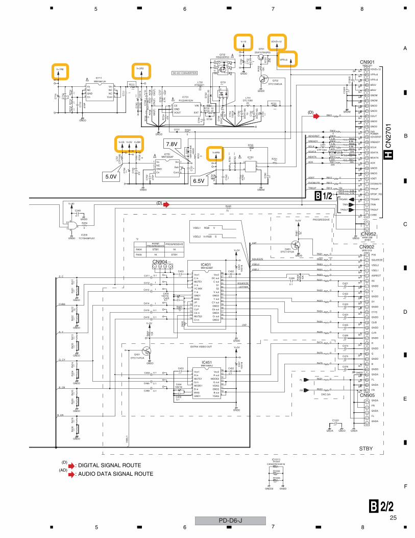
: AUDIO DATA SIGNAL ROUTE(AD): DIGITAL SIGNAL ROUTE(D)
: FOCUS SERVO LOOP LINE(F)
(RF) : RF SIGNAL ROUTE
: TRACKING SERVO LOOP LINE(T)
: STEPPING SERVO LOOP LINE(S)
(S)(S)(S)(S)
(T)(T)(F)(F)
(RF)
(RF)
(F)
(T)
(F)
(F)
(S)
(S)
(S)
(S)
(F)(T)
(T)
(T)
1 2 3 4
C
D
F
A
B
E
23
5 6 7 8
LIM
IT
SYS
VIDEO
AUDIO
20 211918 22 2423
2831 2930 26 2527
32 41
63
62
64
6665 6867 72 737069 71 74 7775 76 8078 8179 868382 84 85 87 908988
61
60
59
56
57
58
55
53
54
92 9391 94 9995 9896 97
101
100
103
102
106
105
107
104
112
109
111
110
108
116
115
113
114
118
117
120
119
125
121
124
122
123
128
126
127
131
130
129
140
132
133
137
138
139
136
134
135
50
51
52
48
49
47
46
45
44
41
43
42
39
40
38
36
37
35
33
32
34
31
29
30
28
27
26
149
148
145
144
147
146
142
143
141
151
150
153
152
154
155
156
157
158
167
164
165
159
160
161
162
163
166
23
25
24
22
21
20
17
18
19
13
14
15
16
10
11
12
7
8
9
6
5
4
3
2
1
256
253
254
255
249
248
252
250
251
246
244
245
247
240
243
242
241
238
236
239
235
237
231
232
233
234
172
176
174
170
175
168
171
169
173
184
181
185
182
183
180
177
178
179
186
228
230
229
227
223
222
225
224
226
219
220
218
221
216
217
214
215
209
211
210
213
212
206
205
208
207
187
188
189
191
190
192
201
204
203
202
200
197
198
199
196
195
193
194
54 1
53
52
51
50
49
48
47
46
44
45
4
2
3
7
5
6
10
11
9
8
41
42
43
38
39
40
35
36
37
14
13
12
16
15
17
18
19
20
33
34
32
31
30
29
28
23
22
21
26
25
24
27
1
2
4
3
R90
8
CN204
R909
R23
2
R23
3 R22
4
C22
0
R21
7
C22
2
C22
3
R23
7
R22
1
R26
1
R25
8
R26
0
R25
9
R23
4
R22
3
C22
4
R23
5
C22
5
C22
7
R22
0
C22
6
R23
6
R23
9 C22
8
C23
0
IC201
C26
9
C26
8
C26
1
R60
2
R60
4R
603
R60
1
R225 C286
C231 R226
R227
C285
C287
C232
C233
R228
R229
C284
IC20
2
C288
C234
R266
C235
R267 R262
C281
C28
2
R28
1
C283
R263
R264
R265
C236
C244
R28
0
R27
9
C242
C243
C23
7
C27
3 C27
1
C27
0
C26
6
C27
2
R25
6
C26
7
C25
9
C25
8
C25
7
C26
0
C25
6
R254
C26
5R25
5
C26
4
C263 C254
C25
5
C26
2
R27
1
R251
L201
C29
8
C29
9
X202
C25
1
X201
R273
C25
3
C24
1
R25
7
R24
8
R24
9
R24
7
R23
8
C24
0C
248
C24
7
C24
6
C23
9
C24
5 C25
0
R24
6
R27
2
R24
5
R25
2R
253
R24
4
R24
1
R24
3
R24
2
R27
0
R23
1
R26
8
R26
9
R23
0
C25
2
R24
0
R209
A8
A7
A6
A5
A4
A2
A3
XR
EA
DY
AD
0
PR
D#
IOW
R#
AD
1
A1
PC
E#
A16
PW
R#
A14
A15
A11
A12
A13
A1
A20
PC
E#
A10
A9
PR
D#
IOC
E#
AD
0
AD
1
AD
4
AD
2
AD
3
AD
5
AD
6
ALE
AD
7
SC
LK
AC
K
MD
AT
A
SD
AT
A
XD
VD
RS
T
A17
A0
UW
R#
UR
D#
SC
L
SD
A
UP
3_1
INT
0#
TR
KU
P
TX
D
RX
D
DQ
6
DQ
M0
DQ
7
DQ
5
DQ
4
DQ
3
DQ
2
DQ
0
DQ
1
DQ
14
DQ
15
DQ11
DQ13
DQ12
DQ9
DQ10
DQ8
DQM1
DRAS#
DCAS#
DWE#
DBA0
DCS#
DQ14
DQ15
MA10
DBA1
DQ13
DQ12
MA1
MA0
DQ10
DQ11
DQ6
DQ7
DQ5
DQ4
DQ2
DQ3
MA3
MA2
DQ8
DQ9
DQM1
MA11
SDCKE
SDCLK
DQ1
DQ0
DQM0
DWE#
DRAS#
DCAS#
DCS#
MA9
MA8
MA11
MA9
MA8
MA6
MA7
MA5
MA6
MA7
MA5
MA4
MA4
DBA1
MA10
DBA0
MA1
MA0
MA2
MA3
I/XP
LETTER
SQUEEZE
VSEL2
VSEL1
AS
PD
IF
AS
DA
T1
AS
DA
T2
AS
DA
T0
AC
LK
ALR
CK
AB
CK
DA
C_X
CS
1
XA
MU
TE
DA
C_S
CK
DA
C_S
O
DA
C_X
CS
0
B_C
B
R_C
R
G_C
Y
CV
BS
S_C
S_Y
RF
IOA
3.3k
GNDD
***
6.8k
V+3DR
0 0
33
0.1
0
0.1
0.1
3333 3333 33 33 33 33
0.1
4.7k
220p
0.1
***
0.01
***
***
0.1
1000
pMT1389EE/B2-L
0.03
3
GNDD
GNDDGNDD
***
***
***
V+5V**
*
RAB4C330J
33*4 0.1
GNDD
0.133
33
0.1
0.1
0.1
0.1 ***
33
0.1
64M
SD
-RA
M
K4S
6416
32K
-UC
75
0.1
0.1
0.1
33
0.1
0 ***
220/4
0
1
***
***
***
0.1
V+3D V+3DR
0.1
***
560F
***
1
220/
4
0.1
0.1
ST
BY
0.1
0.1
15k
1000
p
0.1
1
0.04
7
0.04
7
0.1
0.1
750K
100K 22
p
V1P4
GNDD
1000
p
1
10/1
6
0.47
390p
0.1
0.1
100 ***
***
0
V+3R3
1
ASS7075
***
GNDD
0
0.1
0.1
0
10K
10K
10k
***
0.1
***
0.1
0.1
0.1
***
33 3333 ***
*** 33 3310 33 10
0
100
100
1k 100
***
***
0.01
0
V+3R3V+3V
A4
A5
A7
A6
A3
A1
A2
D0
D8
D1
VS
S
~O
E~
A0
~C
E~
DOWNLOAD
CH:CCSRCH~OTHERS:CKSRYB~
CAPACITOR
(F):RS1/16S****FOTHERS:RS1/16S***J
CKSQ**~
:1608 Size
:2125 Size
:1608 Size
:2125 Size
DIODE
Chip Size
RESISTOR
1SS355
RS1/10S***J
DVSS
APLLVSS
APLLCAP
HIG
HA
6(P
U)
HIG
HA
4(P
U)
HIG
HA
3(P
U)
HIG
HA
5(P
U)
DV
DD
3
HIG
HA
1(P
U)
HIG
HA
2(P
U)
IOA
20
XIO
CS
(P
U)
AD
0
AD
1
DV
DD
3
XIO
OE
IOC
A1
(PU
)
DV
SS
(18
)
AD
4
AD
3
AD
2
IOA
2/V
_AD
IN0
AD
5
ALE
(P
U)
AD
6
IOA19 (PU)
IOA18 (PU)
HIGHA0(PU)
IOA7 (PU)
IOA5 (PU)
IOA6 (PU)
IOA4 (PU)
IOA3 (PU)
IOA2 (PU)
65:A
PLL
VS
SV
DD
3
66:X
IOW
R
67:A
16
68:H
IGH
A7(
PU
)
3.3v
1.8v 1.8v
3.3v
AD
7
A17
XU
WR
(P
U)
DV
SS
(3)
IOA
0 (
PU
)
UP
1_3
(PU
)
UP
1_2
(PU
)
DV
DD
18
XU
RD
(P
U)
UP
1_4
(PU
)
UP
1_7
(PU
)
UP
1_5
(PU
)
UP
1_6
(PU
)
UP
3_4
(PU
)
UP
3_5
(PU
)
UP
3_1
(PU
)
UP
3_0
(PU
)
DV
DD
3
IRICE
(P
D)
XIN
T0
(PU
)
XP
RS
T (
PU
)
DV
SS
(18
)
DQ
S0
DQ
M0
RD
7
RD
6
DV
SS
(3)
RD
3
RD
4
RD
5
DV
DD
18
RD
0
RD
1
RD
2
RD11
RD13
RD12
126:
RD
15
127:
DV
DD
3
128:
RD
14
DQM1
RD10
(3)DVSS
RD9
RD8
XRWE
DQS1
XCAS
XRAS
TCK/V_ADIN6 (JTAG)
DVDD18
TDO/V_ADIN7 (JTAG)
FG/V_ADIN8 (PU)
TMS/V_ADIN5 (JTAG)
TDI/V_ADIN4 (JTAG)
USB_VDD3
USBM
USBP
TRO
FOO
USB_VSS
PWMOUT1/V_ADIN9
TROPENPWM
FMO
OP_INP
OP_INN
DMO
TEO
OP_OUT
TEZISILV
FEO
VREFO
V2O
V2REFO
RFLV/RFON
CSO/RFOP
SGND
XRCS
DVDD3
(18) DVSS
BA0
BA1
(3) DVSS
RA10
RA0
RA1
RA2
DVDD18
RVREFN_ADIN3
RCLKB
DVDD3
RA3
RA11
RCLK
CKE
RA9
RA8
DVDD3
(PU)RD3/ASDATA5
RA4
(18) DVSS
(3) DVSS
RA7
RA6
RA5
SVDD3
LDO1
LDO2
MIDI2
MIDI1
TPI
CDFON
CDFOP
TNI
SD
SC
SB
MD
MC
SA
MB
MA
DVDRFIN IRE
F:2
55
RF
GC
:254
AV
DD
3:25
6
OS
P:2
52
OS
N:2
53
DVDRFIP
DVDD
DVDC
AGND
DVDA
DVDB
CE
QP
RF
GN
D
CE
QN
CR
TP
LP
RF
RP
DC
RF
VD
D3
RF
RP
AC
HR
FZ
C
S_V
RE
FP
S_V
RE
FN
S_V
CM
AD
CV
DD
3
AD
CV
SS
LPF
ON
LPF
IP
LPF
OP
LPF
IN
PLL
VD
D3
JIT
FN
IDA
CE
XLP
PLL
VS
S
(PU) RD30
RD29
(INPUT) RD24
RD25
DVDD18
RD27
RD28
RD26
(3) DVSS
DVDD3
(INPUTPU) RD21
RD22
(INPUTPU) RD20
(INPUTPU) RD19
(INPUTPU) RD18
DACVDDC:189
(INPUTPU) DQM3
(INPUT PU) DQM2
RD23
VREF:190
(3)
D
VS
S
(PD
) A
SD
AT
A4
(PD
) A
SD
AT
A3
(PD
) A
SD
AT
A2
(PD
) A
SD
AT
A1
JIT
FO
XT
ALI
RF
GN
D18
XT
ALO
RF
VD
D18
SP
DIF
MC
_DA
TA
DV
DD
18
(PD
) A
LRC
K
(18)
D
VS
S
(PD
) A
SD
AT
A0
SP
BC
K/A
DA
TA
5
VS
YN
/V_A
DIN
1
HS
YN
/V_A
DIN
2
YU
V7/
AS
DA
TA
5
AC
LK
AB
CK
SP
DA
TA
SP
LRC
K
DV
DD
3
SP
MC
LK
YUV0/CIN:192 (INPUTPU) RD16
(INPUTPU) RD17FS:191
YU
V3/
CV
BS
DV
DD
3
YU
V4/
G
DA
CV
SS
A
YU
V5/
B
YU
V6/
R
DA
CV
DD
A
YU
V2/
C
DA
CV
SS
B
DA
CV
DD
B
YU
V1/
Y
DA
CV
SS
C
STBY
VSS VCC
VSSQ
DQ14
DQ15
DQ12
DQ13
VCCQ
DQ10
VSSQ
DQ11
VCCQ
DQ1
DQ0
DQ3
DQ2
VSSQ
VCCQ
DQ4
DQ5
DQ9
DQ8
VCCQ
VSS
NC
UDQM
CKE
NC
CLK
DQ6
DQ7
VSSQ
VCC
LDQM
WE
CS
RAS
CAS
3.3v
1.8v
A11
A9
A8
A6
A7
A5
VSS
A4
A10/AP
BA0
BA1
A0
A1
A2
VCC
A3
1.8v
3.3v
(27MHz)
(R203)
CONT
GND OUT
VDD
1.8v
DS
D_R
ch controlDAC
3.3v
1.8v
3.3v
to VIDEO PART
(Page 2/2)
to AUDIO PART
(Page 2/2)
B 1/2
2/2B
2/2B
3
2
5
(D)
(AD
)
(D)(AD)
PD-D6-J5 6 7 8
C
D
F
A
B
E
PD-D6-J24
1 2 3 4
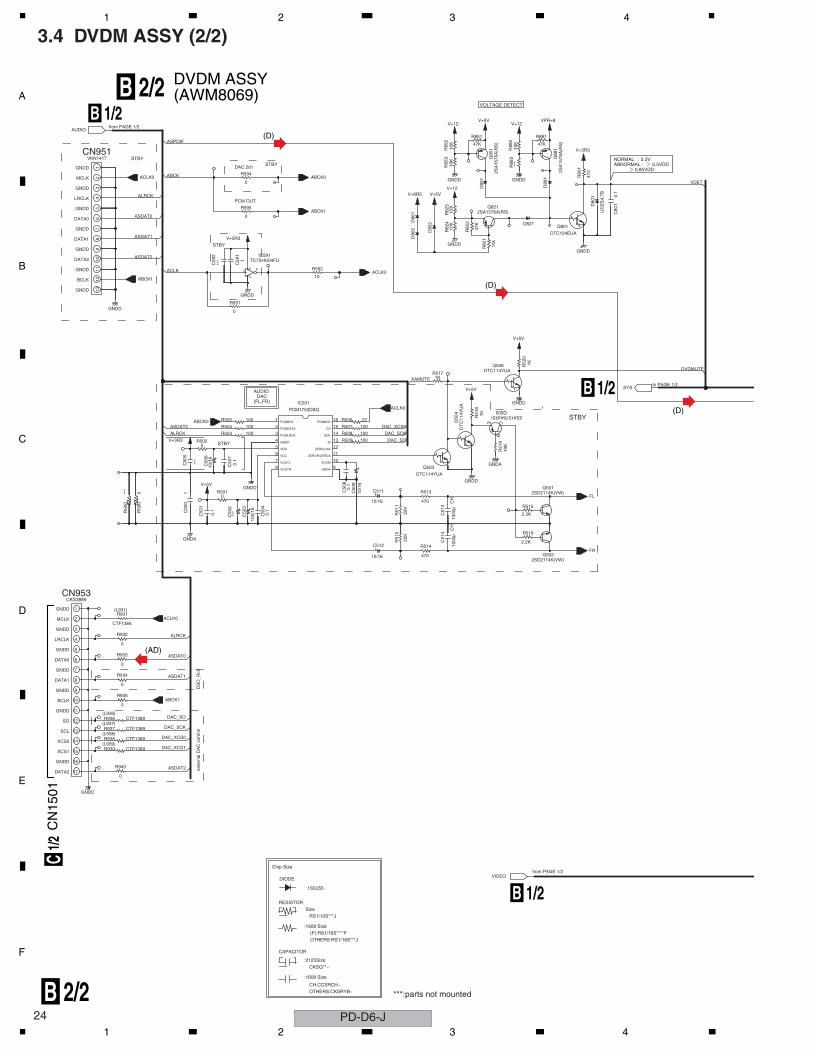
3.4 DVDM ASSY (2/2)
17
16
14
15
12
13
10
11
9
8
7
6
5
4
3
2
1
8
6
7
4
5
3
2
1
1311
12
425
3
10
9
11
14
13
12
16
15
B
E C
105
69
78
32
14
ASDAT2
DAC_XCS1
DAC_SO
DAC_SCK
DAC_XCS0
ASDAT1
ALRCK
ASDAT0
ALRCK
ASDAT0
ACLK
DAC_SCK
DAC_SO
DAC_XCS0
XAMUTE
DVDMUTE
ASDAT1
ASDAT0
ASDAT2
ALRCK
ASPDIF
ABCK
VDET
R940
R939
R938
R936
R937
R935
R934
R933
R932
CN953
R931
R59
0
R50
0
C50
1
C50
0
C50
2
C50
4
C50
3
R501
C50
6
C50
5
C50
7
R502
R503
R504
R505
IC501
R591
C59
2
C59
1
R592
C512
R51
2R
511
R514
C51
4C
513
Q502
R516
C50
8
C50
9
C511 R513
Q503
R51
9R515
Q501
R509
R508
R506
R507
Q50
4
R51
8 Q505
R517
Q506 R52
0
IC591
R595
CN951
R594
D86
2D
861
R82
1
D85
2
R82
4
R82
2
R82
3 Q821
D821Q801
D85
1
R85
3R
852
Q85
1
D88
1
R88
3
R80
1
R88
2
Q88
1
R851 R881
C80
1D80
1
GNDD
0
CTF1389
CTF1389
CTF1389
CTF1389
0
0
0
0
CTF1384
CKS3885
GNDA
0.1
***
100/
16
0.1
0***
1
0
V+5V
***
10/1
6
0.1
GNDD
V+3R30
100
100
100
PCM1753DBQ
GNDD 0
***
GNDD
10
10/16
22K
22K
470
1000
p10
00p
CH
2SD2114K(VW)
2.2K
2.2K
10/1
6
10/16
0.1
470 CH
DTC114YUA
GNDD
GNDA
2SD2114K(VW)
10K
100
100
22
100 DT
C11
4YU
A
1K 2SA1576A(RS)
V+5V
GNDD
DTC114YUA
1K
1K
V+5V
V+3R3
TC7SHU04FU1
0
VKN1417
0
GNDD 10k
10K
47K
15K
2SA1576A(RS)
GNDD
DTC124EUA
V+6R5 V+5VV+12
GNDD
10K
2SA
1576
A(R
S)
10K 47K
GNDD
***
2SA
1576
A(R
S)
470
10K 47K
V+3R3
V+5VV+12 V+12
VPR+8
UD
ZS
4.7B 0.
1
VIDEO
ABCK1
ACLK0
ABCK0
ABCK1
FR
FL
ACLK0
ACLK0
SYS
ABCK1
ACLK0 ABCK0
AUDIO
***:parts not mountedOTHERS:CKSRYB~CH:CCSRCH~
:2125Size
(F):RS1/16S****FOTHERS:RS1/16S***J
:1608 Size
CKSQ**~
:1608 Size
CAPACITOR
Chip Size
RESISTOR
RS1/10S***J Size
1SS355
DIODE
from PAGE 1/2
LRCLK
DATA0
GNDD
GNDD
BCLK
XCS1
GNDD
GNDD
DATA2
XCS0
DATA1
GNDD
exte
rnal
DA
C c
ontr
ol
(L939)
SCL
SO
(L938)
(L937)
(L936)
DS
D_R
ch
GNDD
MCLK
GNDD (L931)
VOUTR
VOUTL
VCC
VCOM
ZEROR/ZEROA
GNDA
STBY
PCMLRCK
PCMDATA
GNDD
VDD ZEROL/NA
PCMBCK PCMMCK
DACAUDIO
(FL,FR)
GNDD
BCLK
GNDD
SCK
CS
SI
STBY
to PAGE 1/2
DATA1
GNDD
DATA0
GNDD
GNDD
DATA2
STBY
PCM OUT
GNDD
LRCLK
GNDD
MCLK
STBY
DAC 2ch STBY
from PAGE 1/2
VOLTAGE DETECT
ABNORMAL : 0.5VDD 0.85VDD
NORMAL : 3.3V
DVDM ASSY(AWM8069)
B 2/2
B 2/21/2B
1/2B
1/2B
CN
1501
C1/2
(D)
(D)
(D)
(AD)
1 2 3 4
C
D
F
A
B
E
25
5 6 7 8
5
8
7
9
10
6
3
5
4
1
2
13
12
11
14
15
16
1 3
14
13
12
11
10
7
8
9
15
16
19
18
17
21
20
22
1
6
4
5
1
2
3
432
24
23
25
26
27
28
2
4
5
4
2
3
5
64
1 7 5
3
4
2
1
27
25
26
24
23
21
22
19
20
17
18
15
16
13
14
12
11
9
10
7
8
6
5
3
4
2
2
1
1
1
2
3
4
2
3
6
5
7
8
9
10
1
12
11
13
14
15
16
3
4 5
6
2
1 8
7
1
3
2
4
5
3
53 4
12
4
21
65
17
18
19
20
22
21
23
24
25
26
27
28
29
VS
EL1
R_CR
B_CB
G_CY
S_Y
I/XP
CVBS
S_C
LETTER
SQUEEZE
VSEL1
VSEL2
SQUEEZE
I/XP
TRKUP
DVDMUTE
VDET
MDATA
ACK
SCLK
SDATA
XDVDRST
XREADY
R43
6R
416
R1003
R1002
R1001
C1001
R43
5R
415
R43
4R
414
R43
3R
413
C466
C455
C465
C464
C454
C453
IC451
C452
C45
1
Q401
R40
1
R40
5
R43
2R
412
R41
1R
431
IC205
C416
C415
C414
R404
C405
C404
C412
C413
C411
CN904
C403
IC401
C402
C40
1
R250
C249
C75
4
L751
R406
C75
2
C75
3
C75
1
C76
1
C76
3
R76
2
R75
0 IC751
R75
1D75
1
R76
4
R76
3 IC761
R765
R522
CN905
R476
R521
C476
C475
R426
R474
R475
C474
C426
C425
R424
R423
R425
C424
C423
C422
C406
R422
R40
2
R421
R403
R924
R923
C421
Q481
R921
R922
R48
1
CN902
CN952
C76
2
R914
R912
R913
R920R915
R761R910
R911
L901
R918
R907
R905
R903
R917
R916
R919
R904
R906
R71
3R
712 C
712
C71
4
C71
3 R71
4
C71
1
IC711
R73
9
R73
6
R73
4
C74
0
C73
9 R73
7
C73
8
D731 R740
C73
6 D733
R733R732
C73
5 C73
4
C73
3
C73
2
R73
8
C73
7R
735
R711
IC731 D73
2
L732
L731
Q731
R70
2
C70
2
C70
1
Q732
Q701
C73
1
R731
R902
R901
Q702
C10
02
C10
03
R70
1
CN901
GNDD
***
***
GNDD2
CKSQYB104K16
GNDD
***
***
***
GNDA GNDAGNDD
GNDD
***
***
GNDD
***
***
GNDD
***
***
GNDD
0.1
0.1
GNDD
0.1
0.1
DTC114YUA
GNDD
100/16
***
MM1566AJ
0.1
100/
16
10K
V+5V
GNDD
***
75
GNDD
***
***
TC7SH08FUS1GNDD
0.1
V+5V
1
0.1
*2
*2
0.1
100/16
1
1
0.1 ***
***
MM1623BF
0.1
100/
16
V+5V
GNDD
0
0.1
V+3D
V+5S
CT
F13
95
75
GNDD
470P
2.2**
*
1
100/
16
***
***
0 MM1565AF
V+5MV+5V
GNDD
1SR
154-
400
0
ST
BY
0
***
V+6R5
***
***
00
***
0
0
*** GNDD
***
0
0
0***
***
***
0
0
0***
***
***
0.1
0
10K
0
0
0
0
***
DTC114YUA
GNDD0
0
1K
GNDD
VKN1319
AKM1288
V+5V
***
GNDM 6.8k10k
3.3k
0
0
***220
220
CTF1334
***
470
3.3k
3.3k
0
22k
***
6.8k
22K
6.8k
***
***
GNDD
470P
***
2.2
***
MM1661JH
V+1R8
18K
(F)
0
47k
27K
(F)
DC
H11
65
0.1
1022
RS
X20
1L-3
0
DC
H11
65 10
DC
H11
65
100/
16
10D
CH
1165
10
22
***
100/
161 10
15K
(F)
120P
2.7K
***
R1224N102H
22
ATH7011
DTL1099
***
GNDD
GNDD
V+3R3
1
***
RSQ035P03
2SA1576A(RS)
V+12
***
***
0
GNDM
10K
DTC124EUA
***
***
47K VPR+8
VDVD+12
VKN1321
FR
FL
TROUT
TRIN
TRGAIN
(C1011)
GNDA
STBY
BIAS
GND1
B in GND2
B out
YSAG
MUTE1
G in
MODE1
R in
Vcc1
G out
MODE2
VSAG
R out
Vcc2
EXTRA VIDEO OUT
MUTE2
Cr in
Cb in
CLP
CY in
BIAS
GND1
I/P
Cr out
GND2
Cb out
GND2
GND2
CY out
GND2
Y out
V in
Y in
YC MIX
Vcc1
MUTE1
C in
S2
S1
V out
Vcc2
DC out
C out
1KR405
R404PROGRESSIVE
except
STBY
*2
1K
VSEL2 V+RGB S
PROGRESSIVE
STBY
VSEL1 RGB V
NCGNDCn
Sub
Cont
Vo Vin
DAC 2ch
GNDA
FL
GNDA
FR
FR
GNDA
FL
GNDA
GNDD
B
GNDD
GNDD
G
GNDD
R
Cr/R
GNDD
Cb/B
GNDD
GNDD
CY/G
SY
GNDD
V
GNDD
SC
ASPECT
VSEL1
VSEL2
STBY
SQUEEZE
P/XI
PROGRESSIVE
CVBS
TROUT
TRGAIN
TRIN
SPDIF_RQ
TRKUP
DVDMUTE
VDET
GNDD
GNDD
ACK
MDATA
SDATA
SCLK
XREADY
XDVDRST
CnGND NC
Cont
NCVo
NCVin
VOUT EXT
CEGND
VIN
DC-DC CONVERTER
GNDD
DVDPOWER
DOUT
GNDD
GNDD
GNDD
GNDM
GNDM
6R5V
6R5V
VPR+8
VPR+8
VDVD+12
B 2/2
1/2B
CN
2701
H
7.8V
6.5V5.0V
: AUDIO DATA SIGNAL ROUTE
: DIGITAL SIGNAL ROUTE(AD)
(D)
(D)
(D)
PD-D6-J5 6 7 8
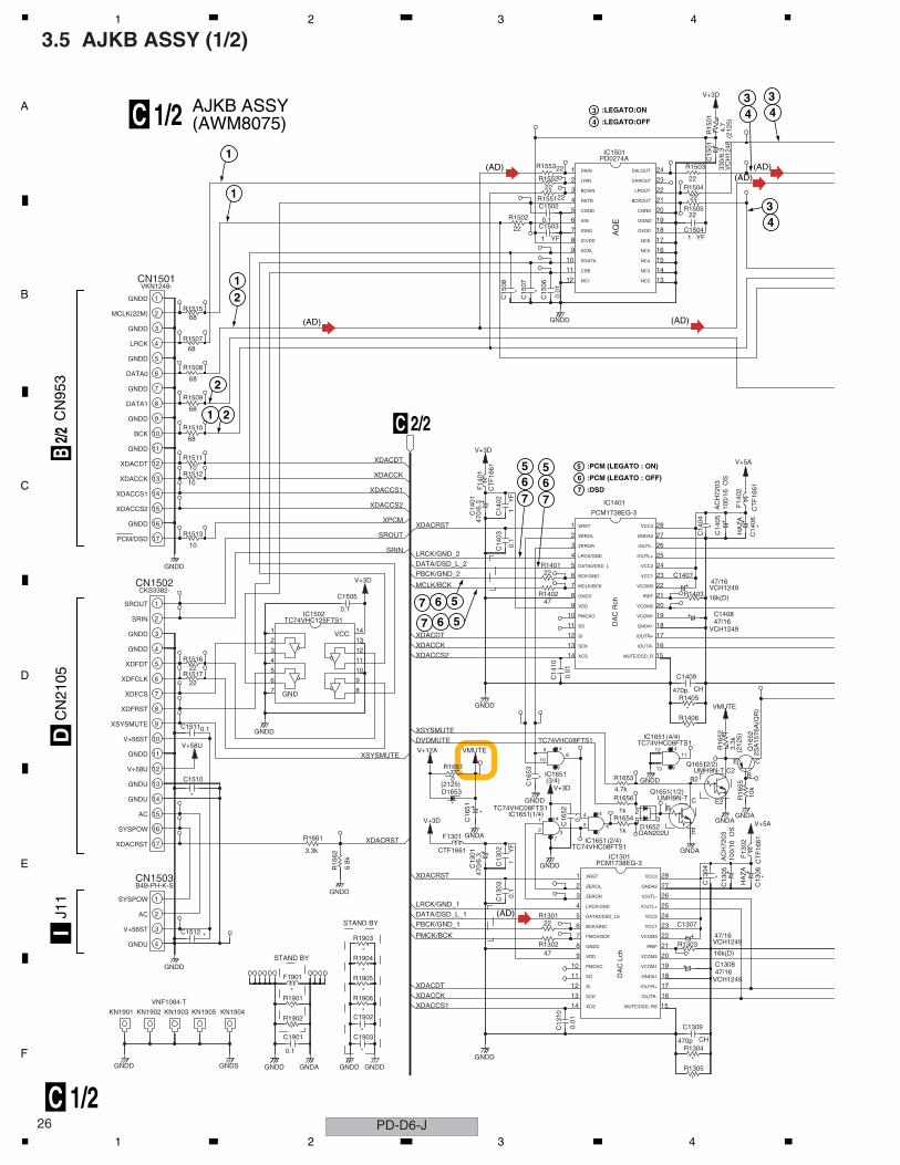
C
D
F
A
B
E
PD-D6-J26
1 2 3 4
3.5 AJKB ASSY (1/2)
DA
C L
chD
AC
Rch
XDACCS1
XDACDTXDACCK
PBCK/GND_1
PMCK/BCK
DATA/DSD_L_1
XDACRST
LRCK/GND_1
XDACRST
XSYSMUTE
XDACCS1
XDACCS2
DVDMUTEXSYSMUTE
XDACCS2
XDACDTXDACCK
DATA/DSD_L_2LRCK/GND_2SRIN
MCLK/BCK
PBCK/GND_2
XDACRSTSROUT
XPCM
XDACDT
XDACCK
4
1
3
2
14
13
12
11
10
8
9
5
7
6
3
4
2
1
15
17
16
19
18
21
20
23
22
24
25
26
28
27
15
16
17
14
12
13
11
10
9
8
7
6 6
7
9
8
5
4
3
2
4
5
2
3
1
11
10
13
12
14
1
17
15
16
14
13
12
11
10
9
8
7
5
6
4
3
2
1
7
2
141
3 7
4
5 6
14
1
2
9
10
7
814
E
B
3
C E2
13 7
B2C2
12 1411
E
B
C
13
12
14
11
10
8
9
6
7
4
5
2
3
1
15
17
16
19
18
21
20
23
22
24
25
26
27
28
11
12
10
9
8
7
5
6
3
2
4
1
14
13
15
16
17
18
20
19
23
22
21
24
GNDU
STAND BY
V+56ST
AC
SYSPOW
STAND BY
XCS MUTE/DSD_RS
SCK
SI IOUTR+
IOUTR-
SO
PMCKO
GNDA1
VCOM1
GNDD
VDD
IREF
VCOM2
PMCK/BCK
DATA2/DSD_LS
BCK/GND
VCOM3
VCC1
VCC2
LRCK/GND
ZEROR
IOUTL+
IOUTL-
ZEROL
XRST
GNDA2
VCC3
AC
SYSPOW
XDACRST
GNDU
GNDU
V+58U
GNDD
V+56ST
XSYSMUTE
XDFRST
XDFCLK
XDFCS GND
XDFDT
GNDD
GNDD
SRIN
VCC
SROUT
PCM/DSD
XDACCS2
GNDD
XDACCS1
XDACDT
XDACCK
GNDD
BCK
GNDD
DATA1
GNDD
DATA0
GNDD
LRCK
MCLK(22M)
GNDD
GNDD
(1/4)
(2/4)
(3/4)
(1/2)
(2/2)
(4/4)
XCS
SCK
SI
MUTE/DSD_R
IOUTR+
IOUTR-
PMCKO
SO GNDA1
VCOM1
VDD
GNDD
VCOM2
IREF
BCK/GND
MCLK/BCK VCOM3
VCC1
DATA0/DSD_L
LRCK/GND
VCC2
IOUTL+
ZEROR
ZEROL
XRST
IOUTL-
GNDA2
VCC3
NC1
CSB NC3
NC2
SDATA
SCKL NC5
NC4
ICVDD
IGND OVDD
NC6
XIN
CGND CGND
OGND
RSTB
BCKIN
BCKOUT
LROUT
LRIN
DAIN
DAROUT
DALOUT
KN1902 KN1903KN1901 KN1905 KN1904
C1901 C1903
R1902 C1902
R1901 R1906
F1901 R1905
R1903
R1904
C1512
CN1503
R1305
C13
10
R1302
R1301
C13
03
R1304
C1309
C1308
R1303
C1307
C13
04
C13
05
C13
06
R16
62
R1661
C1510
C1511
R1517
R1516
IC1502
CN1502C1505
R1513
R1512
R1511
R1510
R1509
R1508
R1507
R1515
F1301
C13
01
C13
02
C16
51
IC1651
IC1301
IC1651
C16
52
D1652R1654
D1653
R1651IC1651
C16
53
R1656
R1653
C14
10
Q1651
Q1651
R16
52
R16
55
Q16
52IC1651
R1406
R1405
R1402
C14
03
R1401
C14
01
C14
02
F14
01
IC1401
C1409
C1408
R1403
C1407
C14
04
C14
05
C14
06
C15
07
C15
08
C15
06
CN1501
C1503R1502
C1502R1551
R1552
R1553
IC1501
C1504
R1505
R1504
R1503
C15
01R
1501
GNDD GNDD GNDDGNDAGNDD GNDS
0.1 *
* *
* *
GNDD
VNF1084-T
* *
*
*
B4B-PH-K-S
*
GNDD
*
GNDD
0.01
47
22
0.1
470/
6.3
*
470p CH
47/16VCH1249
VCH1249
16k(D)
47/16
* *
HA
ZA6.
8k
3.3k
V+58U
*
0.1 GNDD
22
22
TC74VHC125FTS1
CKS3382-
GNDD
V+3D
0.1
10
10
10
68
68
68
68
68
V+3D
CTF1661
1 GNDD
GNDA
YF
* TC74VHC08FTS1
PCM1738EG-3
TC74VHC08FTS1
DAN202U1k
0.1 1k
V+12A
*
(2125)0
GNDD
*
VMUTE
V+3D 4.7kGNDD
TC74VHC08FTS1TC74VHC08FTS1
GNDD
GNDA
GNDAGNDA
V+5A
UMH9N-T
UMH9N-T
3.3k
10k
2SA
1576
A(Q
R)
(212
5)
*
* VMUTE
470p CH
0.01
47
22
0.1
470/
6.3
1
CT
F16
61
YF
PCM1738EG-3
47/16VCH1249
16k(D)
47/16VCH1249
AC
H72
0310
0/16
OS
A
CH
7203
100/
16 O
S
HA
ZA
* *
V+3D
GNDD
* *
0.01
V+5A
VKN1248-
22
YF1
AQ
E0.1
22
22
22
PD0274A
YF1
22
22
22
330/
6.3
VC
H12
48(2
125)
4.7
V+3D
AJKB ASSY(AWM8075)
CN
2105
DJ1
1I
C 1/2
CN
953
B2/2
C 1/2
2/2C
:PCM (LEGATO : OFF)
5
6
7
:PCM (LEGATO : ON)
:DSD
3
4
:LEGATO:ON
:LEGATO:OFF
21
7
7
6
6
5
5
7 6 5
765
134
43
43
1
21
2
F14
02
CT
F16
61
F13
02
CT
F16
61
(AD)
(AD)
(AD)
(AD)
(AD)
(AD)
1 2 3 4
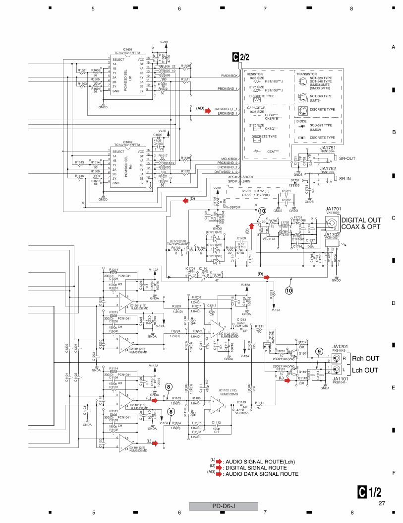
C
D
F
A
B
E
27
5 6 7 8
+
-
+
-
-
+
-
+
+
+
-
-
PC
M/D
SD
SE
LR
chLc
hP
CM
/DS
D S
EL
V+3SPDIF
SPDIF
DATA/DSD_L_2
XPCM
PBCK/GND_2LRCK/GND_2
MCLK/BCK
SRINSROUT
DATA/DSD_L_1LRCK/GND_1
PMCK/BCK
PBCK/GND_1
5
7
4
6 8
34
2
18
2 8
3
1
4
6
54
78
54
34
6
78
2 81
1314
7
1214
7
11 10
114
7
5 14
7 6
2 3 14
7 4
914
7
8
8 9
5
6
7
12
11
10
4
3 14
13
16
15
1
2
B C
E
2
1
3
12
E
B C
1
2
13 2
3
1
4
5
21 4
3 32
1
3
2
1
3
2
1
4
5
6
8
7
13
12
9
10
11
14
16
15
3
1
2
(2/2)
(1/2)
(1/2)
(2/2)
(1/2)
(6/6) (5/6)
(3/6)
(1/6)(2/6)
(4/6)
C1721 R1751(0 )
GND
2Y 3B
3Y
2A
2B
4Y
3A
1Y
1B 4A
4B
*1
1A
SELECT VCC
ST
L
(2/2)
R
C1722 R1752(0 )
DIGITAL OUTCOAX & OPT
SR-OUT
SR-IN
DISCRETE TYPE
CEAT***
DISCRETE TYPE
(UMD2)
4Y
3A
3B
3YGND
2Y
2B
2A
1Y 4B
VCC
ST
1B
1A
SELECT
4A
CKSRYB***CCSR***
2125 SIZECKSQ***
1608 SIZECAPACITOR
(UMT6)
DISCRETE TYPE
DIODESOD-323 TYPE
DISCRETE TYPE
RS1/10S***J2125 SIZE
RS1/16S***J
RESISTOR1608 SIZE
SOT-346 TYPE
(SMD3,SMT3)
TRANSISTOR
(UMD3,UMT3)
SOT-323 TYPE
SOT-363 TYPEC
1120
C11
03
C11
19
IC1101
R1102
R1104
R1108
R1107 C1112
R1115
C1105 C11
08
IC1101
C1109 C
1110
R1103
R11
05
C11
11
R1106
IC1102
C1113 R1111
R11
09
C11
01
C11
02
C12
02
C12
03
C12
01 C12
20C
1219
R1101
C11
06C1104
R1114
C11
07
IC1201 R12
05
C12
11
C11
17
C11
18
IC1102R1202
C12
08
C1205
R1215
IC1201
C1209
R1204
C12
10
R1203
R1206
R1207 C1212
R1201 C12
06
C1204
C12
07
R1208
R1705
R1214 IC1701
R1702
IC1701
IC1701
R1703 R1704
IC1701IC1701
IC1701
C17
04
C17
05
R1616
R1615
R1560
R1613 R1614
R17
01
R1623
R1621
R1622
R1618
R1620
IC1602
R1617R1619
C1603
C1605
Q1101
R1112 C12
14
R1110
C11
14
JA1101
R12
09
D16
51
Q1201R1210
R1212
JA1201
R1211
C1213
C11
15
C11
16 R12
13
C17
11
C17
12C1710 C1716
C17
08
C17
06
C17
07
C1709
L1701 R1706
F1702C1717
C17
13
C17
14
L1702
F1701
JA1702
JA1701
C1722
C1721 C17
53
D1751
C17
51
C17
52
JA1752
JA1751
R1603
R1604
R1605
R1602R1601
R1610
R1612
R1609
R1607
R1611
IC1601
R1606
C16
01
C16
02
R1608
*
GNDA
*
330(D)
*
NJM5532MD
*
CH1500pGNDA
V-12A
100/16
1.2k(D)
1.2k(D)
CH1.8k(D) 470p
PCN1041 0.1
NJM5532MD
*
1.2k(D)
GNDA
CH
1200
p
1.8k(D)
1.2k
(D)
NJM5532MD
VCH1255
NP47/50
750
* *
330(D)
GNDA
*
* *
*
330(D)
CH
1500p 0.1
PCN1041
100/
16
V+12A
CH
470p
*
NJM5532MD
GNDA 1.2k(D)
GNDA
1.2k
(D)
470p
0.1
1.8k(D) CH NJM5532MD
CH1500p
PCN1041
0.1
NJM5532MD
V-12A
100/16
1.2k(D)
1200
p CH
CH1.8k(D) 470p
*
330(D)
1500p
*
0.1
CH
PCN1041
GNDA
100/
16
1.2k(D)
47
V+12A
0 0 22
TC74VHCU04FT
GNDD
0.1
330/
6.3
VC
H12
48
GNDD
*56
22
* 56
(212
5)0
V+3D56
10
100
*
22
10 *
TC74VHC157FTS1
YF1
47/35
V+3D
22k
220
1k
2SD2114K(VW)
GNDA
* *
PKB1041-
V-12A
100/
16
22k
2SD2114K(VW)1k
DA
P20
2U
220PKB1042-
VCH1255
NP 750
47/50
GNDA
100/
16
V-12A
0.1
V+12A
*GNDD
* *47/35
1000p*
YF
147/3
5
1000
p
0.01
VTL1172
75
CTF1661
PTL1017
*
DTF1068
VKS1002
*
VKB1097-GNDS GNDD
*1
GNDS
*1
0.1
1SS355
GNDS
0.011
YF
RKN1004-
YB
RKN1004-
GNDD
56*
22
* 56
56
10*
100
10 *
TC74VHC157FTS1
22
47/3
5YF
1
V+3D
C 1/2
Rch OUT
Lch OUT
2/2C
9
8
8
10
10
: AUDIO SIGNAL ROUTE(Lch)(L)
: DIGITAL SIGNAL ROUTE(D)
: AUDIO DATA SIGNAL ROUTE(AD)
(AD)
(D)
(D)
(L)
(L)
(L)
(D)
PD-D6-J5 6 7 8
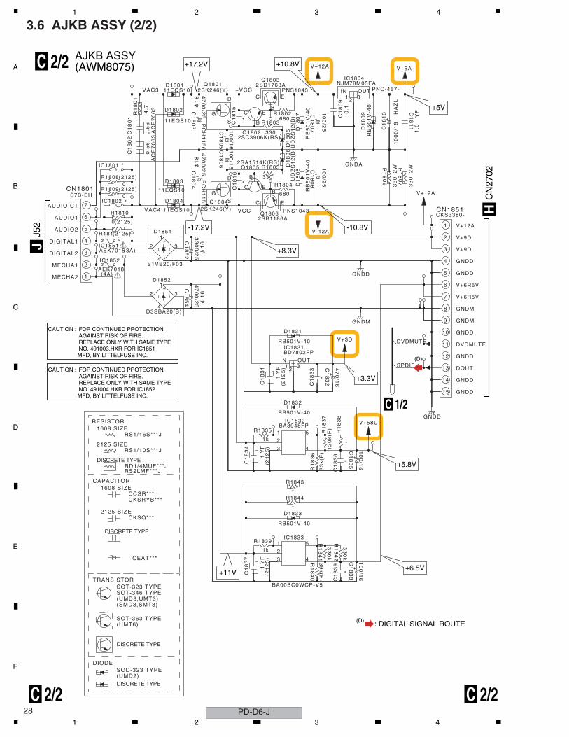
C
D
F
A
B
E
PD-D6-J28
1 2 3 4
3.6 AJKB ASSY (2/2)
+17.2V
-17.2V
+10.8V
-10.8V
+5V
+8.3V
+3.3V
+5.8V
+6.5V+11V
AUDIO2
AUDIO1
SPDIF
DVDMUTE
V+6R5V
GNDM
V+9D
D1852
C1
85
4
IC1851
IC1852
R1811 D1851
R1810
C1
85
2
C1
83
7
C1
83
9
C1
83
8
R1
84
0
R1839 R1
84
1
R1
84
2
IC1833
D1833
R1844
R1843
R1
83
6
C1
83
5
C1
83
6
C1
83
4
R1835 R1
83
7
R1
83
8
IC1832
C1
83
1
D1832
C1
83
2C1
83
3
D1831
IC1831
Q1806CN1851
CN1801
IC1802 D1804
R1809
R1808D1803
IC1801
Q1804
C1
80
4
C1
81
6
C1
80
6
C1
80
2C
18
01
R1
80
1
D1802
C1
80
5
C1
80
3 C1
81
5
D1801 Q1801
R1804 D1
80
8 C1
80
8
R1805Q1805 D1
80
6
R1
80
6
R1
80
7
D1
80
5Q1802
D1
80
7 C1
80
7
R1803
R1802
D1
80
9
C1
81
3C1
80
9
C1
81
1
Q1803 IC1804
D3SBA20(B)
(4A)AEK7018
S1VB20/F03
47
00
/25
AEK7015(3A)
(2125)0
(2125)0
11EQS10
33
00
/25
(21
25
)
BA00BC0WCP-V5
*
39
k(F
)
10
0/1
6
YF
1
1k
RB501V-40
33
0k
33
0k
*
*
33
k(F
)
10
0/1
6(21
25
)Y
F1
1k
BA3948FP
*
12
0k
(F)
*
GNDDV+58U
(21
25
)Y
F1
RB501V-40
47
0/1
6
*
RB501V-40 V+3D
GNDM
BD7802FP
GNDD
V-12A
2SB1186ACKS3380-
S7B-EH*
0(2125)
(2125)0
11EQS10
*
AC
E7
06
3
PC
H1
15
6
2SK246(Y)
47
00
/25
10
0/1
6
0.5
6A
CE
70
63
0.5
64
.7
11EQS10 PC
H1
15
6
10
0/1
6
47
00
/25
11EQS10 2SK246(Y)
680
*
330
RB
50
1V
-40
UD
ZS
12
(B)
2SA1514K(RS)
10
0/2
5
GNDA
V+12A
33
02
W
33
02
W
UD
ZS
12
(B)
2SC3906K(RS)330
RB
50
1V
-40
* 680
10
0/2
5
RB
50
1V
-40
0.1
YF
1.0
10
00
/16
H
AZ
L
2SD1763A
V+12A
NJM78M05FA
V+5A
1
2
4
1
2 3
5
6
3
4
4
2
1
3
3
1
2
4
5
1
2
3 4
5
1 32
15
13
14
11
12
9
10
8
6
5
4
7
2
1
3
7
G
S
D
G
S
D
C E
BE
B
C
C E
B
B
EC2 31
VAC4 -VCC
VAC3 +VCC
(UMD2)DISCRETE TYPE
DIODE
(UMT6)
SOD-323 TYPE
DISCRETE TYPE
TRANSISTORSOT-323 TYPESOT-346 TYPE
(SMD3,SMT3)
SOT-363 TYPE
(UMD3,UMT3)
CKSQ***
CEAT***
DISCRETE TYPE
CAPACITOR
CCSR***1608 SIZE
RS2LMF***J
2125 SIZE
CKSRYB***
RD1/4MUF***J
RESISTOR
DISCRETE TYPE
RS1/10S***J2125 SIZE
RS1/16S***J1608 SIZE
MECHA2
MECHA1
DIGITAL2
DIGITAL1
16
16
DOUT
GNDD
GNDD
PNS1043
GNDD
GNDM
GNDD
DVDMUTE
V+6R5V
GNDD
GNDD
V+9D
V+12A
AUDIO CT
18
18
PNS1043 PNC-457-
+-
~ ~+
-~ ~
OUTIN
OUTIN
J52
J
CN
2702
H
C 2/2 C 2/2
AJKB ASSY(AWM8075)C 2/2
1/2C
(D)
: DIGITAL SIGNAL ROUTE(D)
CAUTION : FOR CONTINUED PROTECTION AGAINST RISK OF FIRE.REPLACE ONLY WITH SAME TYPE NO. 491003.HXR FOR IC1851
MFD, BY LITTELFUSE INC.
CAUTION : FOR CONTINUED PROTECTION AGAINST RISK OF FIRE.REPLACE ONLY WITH SAME TYPE NO. 491004.HXR FOR IC1852
MFD, BY LITTELFUSE INC.
>
>
1 2 3 4

C
D
F
A
B
E
29
5 6 7 8
PD-D6-J5 6 7 8
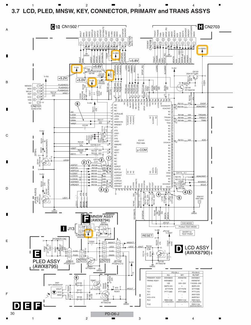
C
D
F
A
B
E
PD-D6-J30
1 2 3 4
3.7 LCD, PLED, MNSW, KEY, CONNECTOR, PRIMARY and TRANS ASSYS
IROUT
LED1
XREADYXDFRSTLCDCK
XDFCSXDFCLK
LCDCS
XDFDT
LED3
LCDDT
VDET
KEY1
XRST
LED1
ACLED2
SRIN
XRST
FLASHDOFLASHCLK
LED2 XRST
MSDCT
SY
SP
OW
XS
YS
MU
TE
SD
AT
AM
DA
TA
SCLK
XDACRST
XDVRST
ACK
TROUTTRIN
TRGAIN
XDACRSTDVDP
FLASHE/D
IRO
UT
SR
IN
XD
FC
LKX
DF
DT
XS
YS
MU
TE
XD
FC
SX
DF
RS
T
FLA
SH
E/D
FLA
SH
CLK
FLA
SH
DO
BLO
FF
LED
3
SP
DIF
_RQ
MS
DC
TD
IMM
ER
XLC
DR
ST
LCD
RS
AC
XD
AC
RS
TS
YS
PO
W
TR
OU
TT
RG
AIN
TR
IN
SP
DIF
_RQ
AC
KS
CLK
MD
AT
A
VD
ET
XR
EA
DY
XD
VR
ST
SD
AT
A
DV
DP
C24
01
W138
C24
02
R24
02
W137
Q2402
R2401
D24
02
2401Q2401
W136
R24
03
C26
02
C26
01
D26
01
R26
01
J2601
Q2501
CN2502J2102CN2503
C21
14
Q2106
C22
18D21
04
C2502
CN2501
C25
01
S2501
Q2104
C21
11
R21
36
R21
38
R21
37
R21
35
D21
02
R2134
R2131
R2133
R2132
Q21
01
R2127
R2130
R2128
R2129
C2110
R21
01D
2101
R2123
R2126 R2122
R2125
C2109
C2216X21
01
R21
21C
2115
C2105
CN2101
R21
71
R2117
R2118
C22
20 C22
17
L210
1
R21
55
R2154
R21
53
C22
19
JP2102
JP2101
R21
46
R21
47
R21
60
C21
12
R21
41
R21
43
R21
42 L210
2
L210
3 KN2101
L2104
L2105
R2175R2112
C2113
PDC148A
IC2101 R2151
R2150
R2149
R2148
R2176
C21
02
R21
62
R21
65
R21
05
R21
06
R21
08
R21
07
R21
10
R21
16R
2163
R21
11C
2103
C21
01
R2104
R2115
R2161
R2140
R21
03
Q2102
D2105
D2103Q2108
C22
26 C22
11
CN
2106
CN
2105
R21
14
R2113 C22
02
Q21030.
1
47/3
5
* RT1P241M
RT1N431M
1SS
355
470
GP1UM28XK0VF
RT1N241M
22K
GNDD
PF02PG-C07
SLR
343B
C4T
47/1
6 270
S2B-PH-K-S B4B-PH-K-SPF04PG-C12
GNDD
V+5U
GNDD
RT1N431M
0.01 *
*
JQ
*
*
VKN2024
V+5U
GNDD
*
VSA1005
SLR
-343
VC
(NP
Q)
RT
1N241M
* 47k
47k
47k
270
220
220
220
220
V+5U
RT
1N24
1M
220
220
220
220
0.01
1kS
LI-3
43U
RC
W(R
ST
)
1M 220
220
47k
AS
S70
34-
0.01
V+5U
10M
Hz
*
220
52492-0720
47K
220
0.04
7FA
CH
1246
V+5U
0.1
22u
100
2.2K
47k
10/5
0
V+5B
V+56ST
10k
10k
220
0.1
220
220
220
CT
F13
89
CT
F13
89
GNDD
VNF1084
CTF1389
CTF1389
0.1
047k
0.1
1M0.
1
220
220
0.1
220
220
220
220
1000
p
100k
220
220
220
220
220
220
*
220
47k
RT1N241M
V+5U
V+5B
1SS355
1SS355
2SC4097(PQR)
V+5U
GNDD
*10k
220
220
220
V+
56ST
V+5U
1
V+58U
GNDD
CK
S38
29
9607
S-1
7F
1k
22k
*
2SA1577(QR)
*
V+SW5U
GNDVCC
VOUT
PLED
V+5U
GNDD
V+5U
S11
H13~H14
FU2
FU1
T51 PTT1369
-
-
-
CN13
T11
120
ATT7079
[POWER-ON]
LED2
MSDCT
[PU
RE
AU
DIO
][S
TB
Y]
WEN/DI
VSS
NC
RST
VCC
WCLK
WD0
RESET
Product TEST MODE
SHORT forTEST POINT
DVD MODE
XREADYXDFRST
NC
NC
LCDCLK
LCDCS
NC
XS
YS
MU
TE
LCD
RS
VS
S4
VD
D4
SY
SP
OW
ST
ES
T
UT
ES
T
NC
NC
NC
NC SCLK
XDVDRST
NC
NC
XDFCLK
LCDDAT
NC
XDFCS
XDFDTNC
NC
NC
NC
NC
SD
AT
A
NC
MD
AT
A
VDD2
VSS2
NC
NC
NC
NC
NC
NC
KEY1VDET
NCSIMUKE
VDD1
µ-COM
DVDACK
NC
NC
NC
NC
NC
CF2
CF1VSS1
XT2
XT1
XRESET FLA
SH
CLK
FLA
SH
DO
FLA
SH
E/D
XLC
DR
ST
NC
NC
NC
NC
TRIN
NC
NC
REMOCON
LED1
LED2ACPULSE
NC
NC
NC LED
3
BLO
FF
DIM
ME
R
MS
_DC
T
SY
SP
OW
2
SP
DIF
_RQ
VD
D3
NC
VS
S3
NC
TROUT
TRGAIN
NC
NC
LCD
RS
DVDON/OFF
XDACRST
NC
NC
NC
NC
NC
SR
IN
IRO
UT
GN
DD
XD
FC
LK
GN
DD
XS
YS
MU
TE
XD
FC
S
XD
FD
T
XD
FR
ST
V+
58U
GN
DD
V+
56S
T
AC
GN
DD
GN
DD
SY
SP
OW
XD
AC
RS
T
TR
OU
T
TR
IN
TR
GA
IN
VD
ET
SP
DIF
_RQ
GN
DD
GN
DD
MD
AT
A
AC
K
XD
VD
RS
T
SD
AT
A
SC
LK
XR
EA
DY
DV
DP
OW
ER
GN
DD
1
3
2
E
2 2C
1 1
B
4
3
4
3
2
1
2
2
13
1 5
64
6
7
4
5
2
3
1
2
1
3231 353433
2930
2628
27
383736 39 4140 42 43 44 45 46 47 4948 50
5152
5354
55
2425
2223
2120
5957
6061
5856
1918
1716
1514
13
6465
6667
6862
63
1112
109
78
6970
7372
7471
56
43
21
7576
7877
7980
100 99 969798 9495 93 91 9092 8889 87 86 85 84 8183 82
E
C B
21
4
3
65
87 9 11
1210
13 15
14
17
16 14
15 13
10
1112
9 78 6
5 3
4 21
PTT1368
REK1134
-
-
(500mA/250V)-
220~230
AWX8799
ATT7078
PTT1370
REK1023
AKX1033
AKR7001
(1.25A/250V)REK1134
(500mA/250V)
AWX8797110/220~240
B3P5-VH
AWX8801
ATT7080
AWX8802
PRIMARY ASSY
TRANS ASSY
AWX8800
PD-D6-J PD-D6-S
REK1058(1.25A/250V)
B2P3-VH
WY RLFWPKU
+5.6V
+5.2V +5.0V
+5.8V
6
1212
3 4 5
54
3
6
FED
D LCD ASSY(AWX8790)
F MNSW ASSY(AWX8794)
EPLED ASSY(AWX8795)
CN2703HCN1502C 1/2
J13I
1 2 3 4
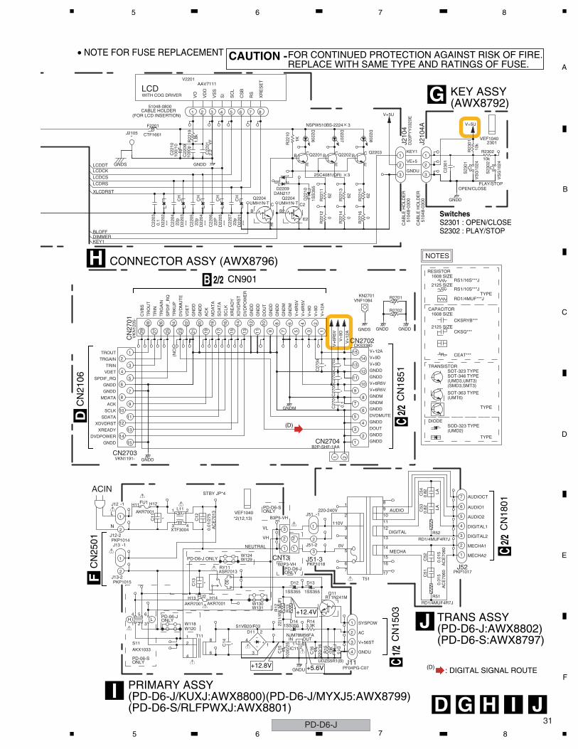
C
D
F
A
B
E
31
5 6 7 8
(D)
: DIGITAL SIGNAL ROUTE(D)
KEY1DIMMERBLOFF
XLCDRST
LCDDTLCDCKLCDCSLCDRS
T11
C14
D11
C15 IC11
C16 R15
W118W120
D14 R14
R13R12
Q11
J11
D15
R51
J13-2
J12-2
J13 -1
C11
J12 -1 H11 H12
C13
RY11
W124W129
D12 D13
CN13 J51-3
L11
C12
J51-2
J51 -1
CN2703
CN2704
C27
04
CN
2701
C22
03
C22
04
D22
02
D22
03
C22
05
C22
06
D22
04
D22
05
C22
07
D22
01
Q2204
R22
12
Q2204 D22
10
R22
11
T51
C51
C52
J52
R52
C53
C54
R2702
R2701
C27
01C
2705
C27
02C
2703
CN2702
KN2701
R22
14
R22
16
R22
13
R22
15
J2105
F2201
C22
09D2209
C22
10
C22
01
R22
19
R22
10
Q2201
D2206
V2201
C23
01
S23
01
S23
02
D2207
Q2202 Q2203
D2208
J210
4
J210
4A
R23
01 2301
R2302
*
GNDU
UDZS5R1(B)
1000
/25
220/
16
10K
NJM78M56FA
S1VB20/F03 1SS35522(1
/4W
MU
F)
3.3K
*
1SS355 1SS355RT1N241M
PF04PG-C07
PKP1015
PKP1014
AKR7001
*
ASR7013
PKP1018
XTF3004 AC
E70
130.
01/2
75* B3P5-VH
VKN1191- GNDD
B2P-SHF-1AA
GNDM
*
VK
N12
05-
***
0.1
22p
***
22p
***
CH
CH
22P
***
***
22p
CH
UMH1N-T
CH
0
UMH1N-T
1SS
355
AC
E70
600.
015
AC
E70
600.
015
PKP1017
RD1/4MUF4R7J
0.82 LA
0.82 LA
GNDD GNDD
*
*
0.1
**
*
V+
6R5V
V+
9D
V+
12A
CKS3380
GNDS
VNF1084
0 0
GNDD
* CTF1661
51048-0800
100/
10
1000
p
GNDD
DAN217
62
2SC4081(QR) 3
YF
2.2
1.8k
1K
NSPW510BS-2224 3
62 62
VS
G10
24
VS
G10
24*
10k
V+5U
D20
PY
Y03
20E
10k
V+5U
+-~
~
OUTIN
GNDU
V+56ST
AC
SYSPOW
ACINFU1
B2P3-VH
VL
VH
NEUTRAL
*2(12,13)VEF1040 220-240V
STBY JP*4
XREADY
XDVDRST
DVDPOWER
GNDD
SCLK
MDATA
SDATA
GNDD
GNDD
ACK
SPDIF_RQ
VDET
TRGAIN
TRIN
TROUT (NC
)
CV
BS
TR
OU
T
TR
IN
SP
DIF
_RQ
TR
KU
P
TR
GA
IN
DV
DM
UT
E
GN
DD
VD
ET
AC
K
GN
DD
MD
AT
A
SD
AT
A
SC
LK
XR
EA
DY
DV
DP
OW
ER
GN
DD
XD
VD
RS
T
GN
DD
DO
UT
GN
DD
GN
DM
GN
DM
GN
DD
V+
6R5V
V+
6R5V
V+
9D
V+
9D
V+
12A
MECHAMECHA2
0V
110V
DIGITAL
AUDIO
DIGITAL2
MECHA1
DIGITAL1
AUDIO1
AUDIO2
AUDIOCT
GNDD
DOUT
GNDD TYPE
DIODESOD-323 TYPE(UMD2)
TYPEGNDD
GNDD
DVDMUTE
GNDM
GNDM
V+6R5V
V+6R5V
(UMT6)SOT-363 TYPE
(SMD3,SMT3)(UMD3,UMT3)
TRANSISTORSOT-323 TYPESOT-346 TYPE
GNDD
GNDD
V+9D
V+9D
V+12A
2125 SIZECKSQ***
CEAT***
CAPACITOR1608 SIZE
TYPE
2125 SIZE
CKSRYB***
RS1/10S***J
RD1/4MUF***J
NOTES
1608 SIZERESISTOR
RS1/16S***J
5104
8-03
00
CA
BLE
HO
LDE
R51
048-
0300
CA
BLE
HO
LDE
R
GNDS
(FOR LCD INSERTION)CABLE HOLDER
LCD WITH COG DRIVER V
DD
VO
AAV7111
VS
S
SI
CS
B
SC
L
RS
XR
ES
ET
GNDU
VE+5
OPEN/CLOSEPLAY/STOP
KEY1
VEF1040
81
4
2
6 3
41
2
21 3
4
2
3
1
2
1
2
1
1 13
3 4
1 2
2 2 2
31
12
15
13
14
10
78
6
11
9
5
4
3
21
2729
28 26 24
25
22
23 21
1819
20
17
16
15 13
1214
1110
9
8 6
7 3
4
5 1
2
B
E
C
B2
E2
C2
6
717
16
5
15 1
4
14
13
3 12
11
2 10
9
2
3
4
6
5
81
7
21
1
3
4
2
56
78
10
9
1112
13
14
15
123
E
B B
1 32 54 76 8
C
E E
B
3 3
2 2
C C 11
RD1/4MUF4R7J
S11
>
>>
>
>
H13 H14W130W131
AKX1033
AKR7001 AKR7001
H LPD-06-J ONLY
PD-06-S ONLY
FU2
PD-D6-J ONLY
1 32
4 5 6
PD-D6-S ONLY
PD-D6-J ONLY
+12.4V
+12.8V +5.6V
L
N
>
>
>
>
>
>
>
JIHGD
G KEY ASSY(AWX8792)
J TRANS ASSY(PD-D6-J:AWX8802)(PD-D6-S:AWX8797)
I PRIMARY ASSY(PD-D6-J/KUXJ:AWX8800)(PD-D6-J/MYXJ5:AWX8799)(PD-D6-S/RLFPWXJ:AWX8801)
H CONNECTOR ASSY (AWX8796)
CN
1851
C2/2
CN
1801
C2/2
CN
1503
C1/2
CN901B 2/2
CN
2106
DC
N25
01F
• NOTE FOR FUSE REPLACEMENT FOR CONTINUED PROTECTION AGAINST RISK OF FIRE.REPLACE WITH SAME TYPE AND RATINGS OF FUSE.
CAUTION -
SwitchesS2301 : OPEN/CLOSES2302 : PLAY/STOP
PD-D6-J5 6 7 8
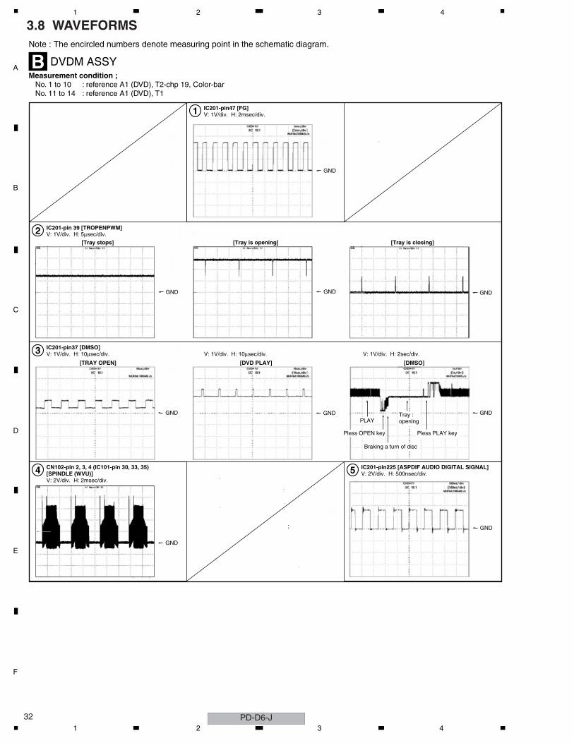
C
D
F
A
B
E
PD-D6-J32
1 2 3 4
3.8 WAVEFORMSNote : The encircled numbers denote measuring point in the schematic diagram.
Measurement condition ;No. 1 to 10 : reference A1 (DVD), T2-chp 19, Color-barNo. 11 to 14 : reference A1 (DVD), T1
DVDM ASSYB
2 IC201-pin 39 [TROPENPWM]V: 1V/div. H: 5µsec/div.
3 IC201-pin37 [DMSO]V: 1V/div. H: 10µsec/div. V: 1V/div. H: 10µsec/div. V: 1V/div. H: 2sec/div.
1 IC201-pin47 [FG]V: 1V/div. H: 2msec/div.
4 CN102-pin 2, 3, 4 (IC101-pin 30, 33, 35) [SPINDLE (WVU)]V: 2V/div. H: 2msec/div.
GND
GND GND GND
GNDGNDGND
GND
PLAYTray :opening
Pless OPEN key Pless PLAY key
Braking a turn of disc
[Tray stops]
[TRAY OPEN] [DVD PLAY] [DMSO]
[Tray is opening] [Tray is closing]
5 IC201-pin225 [ASPDIF AUDIO DIGITAL SIGNAL]V: 2V/div. H: 500nsec/div.
GND
1 2 3 4
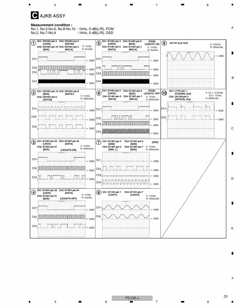
C
D
F
A
B
E
33
5 6 7 8
1Ch1: CN1501-pin 4 [LRCK]Ch2: CN1501-pin 10 [BCK]
Ch3: CN1501-pin 6 [DATA0]
Ch1: CN1501-pin 10 [BCK]Ch2: CN1501-pin 6 [DATA0]
Ch3: CN1501-pin 8 [DATA1]
Ch1: IC1501-pin 22 [LRCK]Ch2: IC1501-pin 21 [BCK]
Ch3: IC1501-pin 24 [DATA]
Ch1: IC1501-pin 22 [LRCK]Ch2: IC1501-pin 21 [BCK]
Ch3: IC1501-pin 24 [DATA]
Ch4: CN1501-pin 2 [MCLK]
Ch1: IC1401-pin 4 [LRCK] JA1101 [Lch Out]
Ch3: IC1401-pin 6 [BCK]
Ch2: IC1401-pin 5 [DATA]
Ch4: IC1401-pin 7 [MCLK]
Ch1: IC1401-pin 4 [LRCK]
Ch3: IC1401-pin 6 [BCK]
Ch1: L1701-pin 1 [COAXIAL Out]Ch2: JA1702-pin 3 [OPTICAL Out]
Ch2: IC1401-pin 5 [DATA]
Ch1: IC1401-pin 4 [GND]
Ch3: IC1401-pin 6 [GND]
Ch1: IC1101-pin 1 [LOUT1]
Ch3: IC1101-pin 7 [LOUT2]
Ch4: IC1401-pin 7 [MCLK]
Ch2: IC1401-pin 5 [DSD_L]
Ch4: IC1401-pin 7 [BCK]
V: 1V/div. H: 2us/div.
V: 1V/div. H: 2us/div.
V: 1V/div. H: 2us/div.
V: 1V/div. H: 500ns/div.
V: 1V/div. H: 500ns/div.
V: 10V/div. H: 500us/div.
V: Ch 1 0.5V/div. Ch 2 1V/div. H: 200ns/div.
V: 1V/div. H: 500ns/div.
V: 1V/div. H: 500us/div.
V: 1V/div. H: 500ns/div.
5 9
6 10
GND
GND
GND
2
3
4
7
8[LEGATO:OFF]
[LEGATO:ON]
[PCM]LEGATO: ON
[PCM]LEGATO: OFF
[DSD]
GND
GND
GND
GND
GND
GND
GND
GND
GND
GND
GND
GND
GND
GND
GND
GND
GND
GND
GND
GND
GND
GND
GNDGND
GND
GND
GND
Ch1
Ch2
Ch3
Ch1
Ch2
Ch3
Ch1
Ch2
Ch3
Ch1
Ch2
Ch3
Ch4
Ch1
Ch2
Ch3
Ch4
Ch1
Ch2
Ch1
Ch2
Ch3
Ch4
Ch1
Ch2
Ch1
Ch2
Ch3
Ch4
AJKB ASSYCMeasurement condition ;No.1, No.3-No.6, No.8-No.10 : 1kHz, 0 dB(L/R), PCMNo.2, No.7-No.9 : 1kHz, 0 dB(L/R), DSD
PD-D6-J5 6 7 8
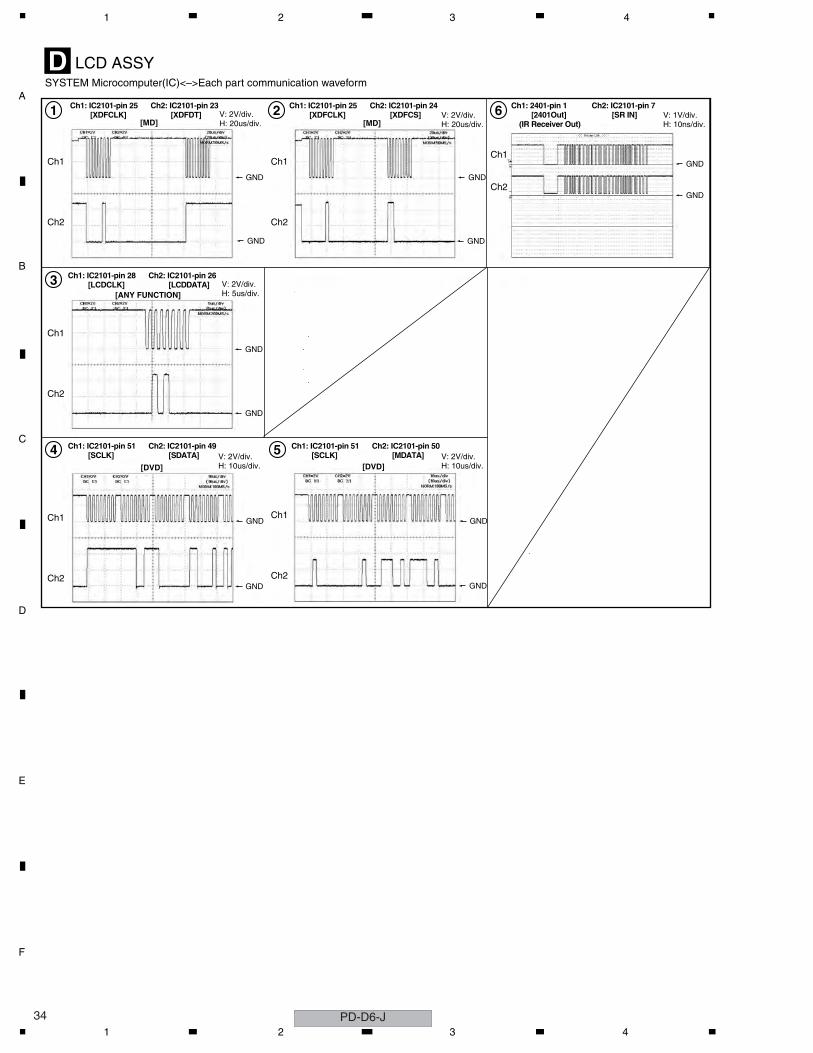
C
D
F
A
B
E
PD-D6-J34
1 2 3 4
1 2
GND
GND
[MD]
3[ANY FUNCTION]
4 5[DVD] [DVD]
[MD]
GND
GND
GND
GND
GND
GND
GND
GND
GND
GND
Ch1: IC2101-pin 25 [XDFCLK]
Ch2: IC2101-pin 23 [XDFDT]
Ch1: IC2101-pin 28 [LCDCLK]
Ch2: IC2101-pin 26 [LCDDATA]
Ch1: IC2101-pin 51 [SCLK]
Ch2: IC2101-pin 49 [SDATA]
Ch1: IC2101-pin 51 [SCLK]
Ch2: IC2101-pin 50 [MDATA]
Ch1: IC2101-pin 25 [XDFCLK]
Ch2: IC2101-pin 24 [XDFCS] V: 2V/div.
H: 20us/div.
6 Ch1: 2401-pin 1 [2401Out] (IR Receiver Out)
Ch2: IC2101-pin 7 [SR IN] V: 1V/div.
H: 10ns/div.V: 2V/div. H: 20us/div.
V: 2V/div. H: 10us/div.
V: 2V/div. H: 10us/div.
V: 2V/div. H: 5us/div.
Ch1
Ch2
Ch1
Ch2
Ch1
Ch2
Ch1
Ch2
Ch1
Ch2
Ch1
Ch2
LCD ASSYDSYSTEM Microcomputer(IC)<–>Each part communication waveform
1 2 3 4
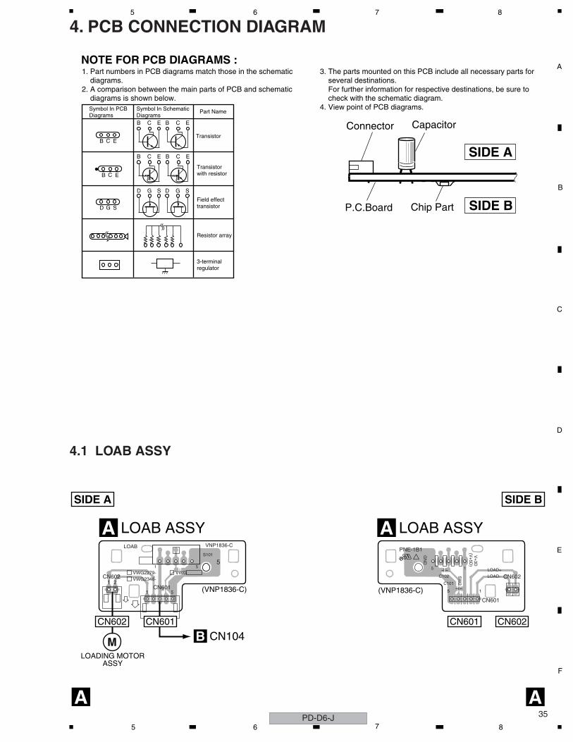
C
D
F
A
B
E
35
5 6 7 8
4. PCB CONNECTION DIAGRAM
4.1 LOAB ASSY
NOTE FOR PCB DIAGRAMS :1. Part numbers in PCB diagrams match those in the schematic diagrams.2. A comparison between the main parts of PCB and schematic diagrams is shown below.
3. The parts mounted on this PCB include all necessary parts for several destinations. For further information for respective destinations, be sure to check with the schematic diagram.4. View point of PCB diagrams.Symbol In PCB
DiagramsSymbol In SchematicDiagrams
Part Name
B C E
D
D
G
G
S
S
B C E
B C E
D G S
B C E B C E
B C E
Transistor
Transistorwith resistor
Field effecttransistor
Resistor array
3-terminalregulator
CapacitorConnector
P.C.Board Chip Part
SIDE A
SIDE B
15
5 1
SW
2
(V+
5D)
V+
3D
LOAD-
LOAD+
GN
D
PNE-1B1
C102
C101
CN602
CN601
1 2
51
VWG2346-VWG2279-
5
VWG
LOAB
51
VNP1836-C
CN602
S101
CN601
SIDE A SIDE B
LOAB ASSYA LOAB ASSYA
CN104B
(VNP1836-C) (VNP1836-C)
LOADING MOTORASSY
M
CN601CN602 CN601 CN602
A A
PD-D6-J5 6 7 8
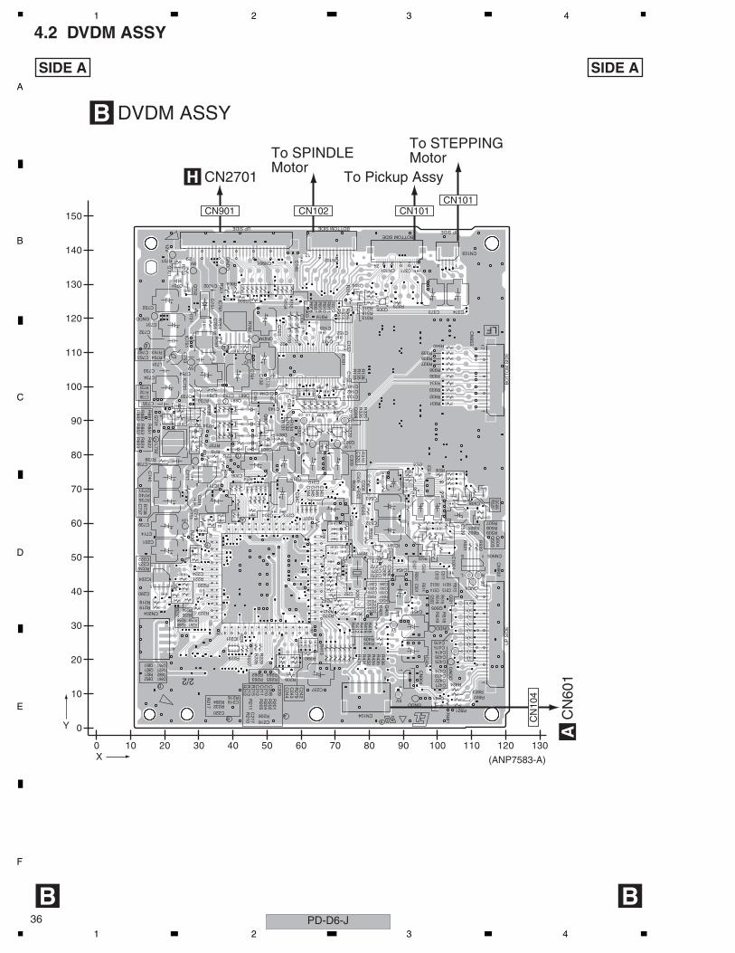
C
D
F
A
B
E
PD-D6-J36
1 2 3 4
4.2 DVDM ASSY
0 10 20 30 40 50 60 70 80 90 100 110 120 130
0
10
20
30
40
50
60
70
80
90
100
110
120
130
140
150
X
Y
C474
C476
C451
C454
CN
902
R915
R914R919
Q731
R906
C426
R904
C425
C423C424
C422C421
L751
R712
Q702
C761
R714
R713C712
D821
C133
R404
C374
R214
R520
Q851
R852
CN101
R220
R237
R284
R221
C215
C217
C104
C216
C244
R232
R216
R207
R209
C220
C213
R217
R235
R211
R134
R136
C161
R154
C143
C142C141
C144
R135
C146
R132
R133
C152
R153R152
R405
R210
CN
904
R269R270
CN905
CN901
C320
C347
R225
C222C223
C224IC204
R224
R918 R
913R
912R
911R
910
D733
CN102
R228
R411
R226
R227
C1002
C1001
R821
R435
R415
R414
C290
R433
D852
Q801
R882
R801
R701
R702
C701
R736
R751
R711
R413 R
436
R907
R750
R824
D881
D862
R823
R851
R822 C801
D801
Q701
C702
R739
L731
L732
R737
C738
C711
R434
R431
R412
R432
R761
R731 C
751
C733
Q305
C371
R325
CN104
C309
CN103
R265R264
R263R262
Q505
R519
C509
Q506
IC761
R762
C345
R416
Q881
R763
C373
R516
C511
R511C
506
R481
Q481
Q401
R507
C514
R401
C753
R733
R740
C752
R738
C736
D731
D751
R732
R735
R734
C754
IC751
C735
C739
C731
C714
C713
C732
C740
C734
IC501
Q501
Q502
R513
R502
C507
IC201
R313
R508
IC731
R901
R229D851
R903
D861
C737
Q821
IC711
R931
R932
R933
R934
R935R936
R937R938R939
R940
R373
C762C763 R764
R595
R594
IC101
CN
953
C505
Q504
R515
R514
C508
Q503
R503
R518
R512
R505
C501
C502
R506
R501
C513
R504
R591
C503
R234
C145
C504
R314
Q304
R315
L309 L308
R326
R881
R258
R602
R213
R601
R212
R200
C101
R131
C131
R261
C310
R151
R310
R321
Q308
R322
R260
C404
R259
C219
R218R219
R509
C512
C102
C132
C140
C242
C243
C151
IC591
R280
C153
C103
Q307
C346
R318
R905
R246R245R244R243
R242
R241
C206
C204C
203
R223
C221
C237
C201
C202
C273
R256
C272C271C270
C269
C268
C267 C265C263 C262
C259
R253
C258R252
CN204
R251
C251
X201
C252
R204
C210
C212
C211
C208
C209
R206
R205
R202
R201
C343
C344
R592
R853
R883
R522
R521
R279
R215
R924
R922R923
R921
C475
UP SIDE
12
7
21
5 3
GN
DD
GNDD
124
BOTTOM SIDE
41
5 1
129
V
5 8
14
R
UP
SID
EG
ND
D
12V
1.8V
3.3V
5V
GNDM
6.5V
BOTTOM SIDE
BO
TT
OM
SID
E
8V
GNDD
3.3V
5V
L
GNDD
R
GNDA
5V
2/2
112
543
1
1 5
4 1
UP SIDE
14
57
1
9
129
12865
64
256193192
1
C
LD_CD
LD_D
VD1
345
A
A
B
B
C
D
D
E
8
54
1
E122 1
71
4
31
5
1
4
3.3V
LF
SIDE A
B
SIDE A
B
CN2701H
CN901
CN
601
A
CN
104
CN101
To SPINDLEMotor
To Pickup Assy
CN101
To STEPPING Motor
CN102
DVDM ASSYB
(ANP7583-A)
1 2 3 4
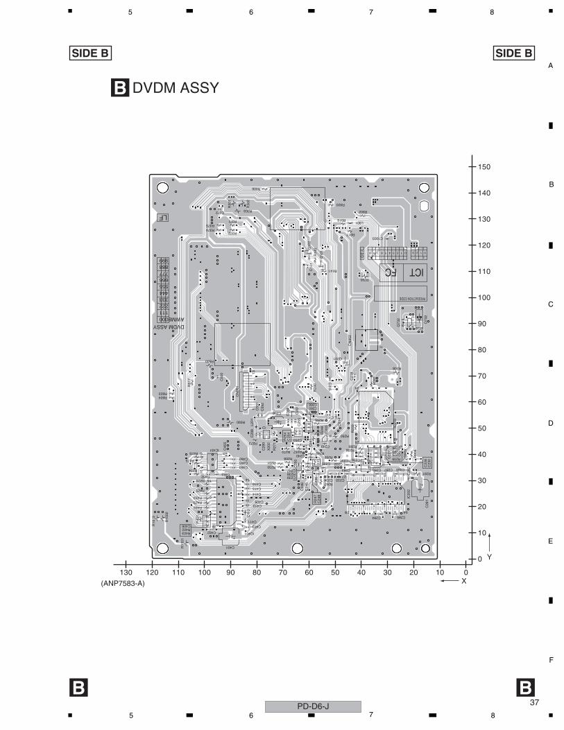
C
D
F
A
B
E
37
5 6 7 8
0102030405060708090100110120130
0
10
20
30
40
50
60
70
80
90
100
110
120
130
140
150
X
Y
164
3
LF
48
124
25
11
3
ABC
1 0
0
3 2 1 09 8 7 6 5 4 3 2 1 0
1
18
16
9
54
127
28
28 1
1415
31 5
4
ICTFC
21
DVDM ASSYAWM8
999888777666555444333222111000
PRODUCTION CODE
C466
C45
5
C464
C452
C465
C453
Q73
2
R403
L901
R10
02
C25
0
R257
C207
C21
4
R236R249
R24
7
C24
6C
245
R285
R238
R208
R23
3
R267
R10
03
R10
01
C22
8
C226C225C289
IC20
3
R917
R266
D73
2
CN
951
R500
R272X20
2
L201
C29
8
C29
9C283
C234
C287
C232
C286
C285
C231R268
IC451
R590
R28
2
C28
2
C406R402
R423
R42
1
R422
R604
C403
R27
1
IC20
2
C59
2
IC401
C401
R426
C372
R273
R375
C405
C402
C41
2
R425
R424
R902
C233
C284
R90
8
R90
9
R920
C1003
R51
7
C249
R476
R475
R474
C23
6
C28
1
C235
IC20
5Q
101
Q10
2
C50
0
R141
R14
2
R406
R250
R374
C415
R281
R603
C23
0
C414
C413
R765
C416
C21
8
C59
1
C22
7
C12
1
C288
R231
C205
R255
C266
C26
4
C260
C26
1C
255
C256
R25
4C
254
R230
C239
C240
C24
1C253
C257R
240
R372
R371
C247
C24
8
C296
R239
R916
C411
R24
8
R30
1
R30
2
Q201
R303
CN
952
SIDE B SIDE B
(ANP7583-A)
B B
DVDM ASSYB
PD-D6-J5 6 7 8
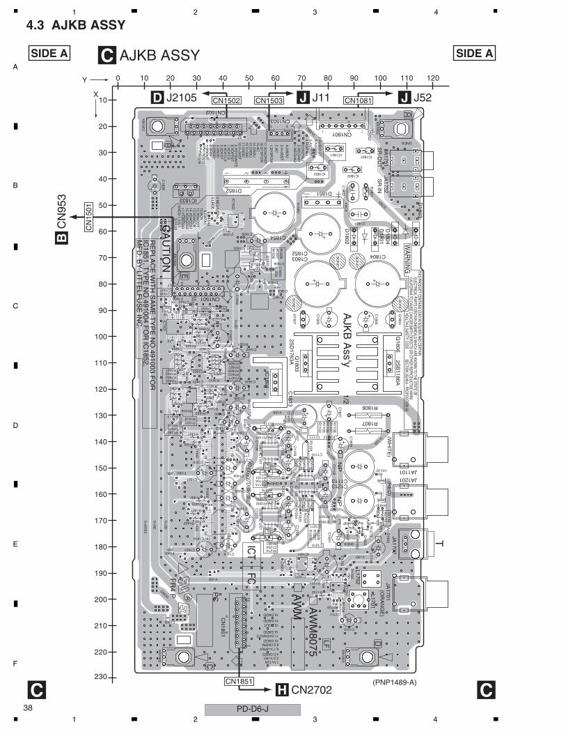
C
D
F
A
B
E
PD-D6-J38
1 2 3 4
4.3 AJKB ASSY
10
20
30
40
50
60
70
80
90
100
110
120
130
140
150
160
170
180
190
200
210
220
230
0 10 20 30 40 50 60 70 80 90 100 110 120
X
Y
281514
1
2815
141
58
1 4
814
1 7
NP
NP
NP
85
4 1
58
1 4
T
178
14
9161
8
9161
8
13
12 1
24
117
V+3D
V+
58U
V+
9D
V+
6R5V
GNDD
V+
3D
V+12A
171
V-12A
VAC3
41
VA
C4
V+5A
GNDS
WAR
NIN
G
GNDA
ELECTRICAL PARTS CONTAIN CHEMICALS W
HICH ARE KNOWN TO THE STATE OF
CALIFORNIA TO CAUSE CANCER,BIRTH DEFECTS OR OTHER REPRODUCTIVE HARM.
HEALTH & SAFETY CODESECTION 25249.6 - PROPOSITION 65
GNDA
71
15
1
7114
8
MF
D. B
Y LIT
TE
LFU
SE
INC
.
V+
3D
SR
-OU
TS
R-IN
AW
M8075
AJK
B A
ss'y
LF
ICT
FC
1/2
AW
M2S
D1763A 2S
B1186A
V+3D
PC
17.PC
M/D
SD
15.XD
AC
CS
214.X
DA
CC
S1
13.XD
AC
CK
12.XD
AC
DT
10.BC
K8.D
AT
A1
6.DA
TA
04.LR
CK
2.MC
LK(22M
)
GN
DD
:1,3,5,7,9,11,16
15.GNDD
14.GNDD13.DOUT
12.GNDD11.DVDMUTE10.GNDD8,9.GNDM6,7.V+6R5V
4,5.GNDD2,3.V+9D1.V+12A
7.AU
DIO
CT
6.AU
DIO
1
5.AU
DIO
24.D
IGITA
L13.D
IGITA
L22.M
EC
HA
11.M
EC
HA
2
4.GN
DU
3.V+
56ST
2.AC
1.SY
SP
OW
17.XD
AC
RS
T16.S
YS
PO
W15.A
C14.G
ND
U13.G
ND
U12.V
+58U
11.GN
DD
10.V+
56ST
9.XS
YS
MU
TE
8.XD
FR
ST
7.XD
FC
S6.X
DF
CLK
5.XD
FD
T4.G
ND
D3.G
ND
D2.S
RIN
1.SR
OU
T
BO
ND
(WH
ITE
)(R
ED
)(O
RA
NG
E)
CA
UT
ION
RE
PLA
CE
WIT
H S
AM
E T
YP
E N
O.491003 F
OR
IC1851, T
YP
E N
O.491004 F
OR
IC1852,
BO
ND
BO
ND
BO
ND
R
FR
4 P
V+58U
V+3D
THIS PRODUCT CONTAINS LEAD IN SOLDER AND CERTAIN
C1108
R1105
R1208
R1107
C1301
IC1301
C1306
C1653
R1307
IC1401
C1207
C1206
R1110
R1407
C1704
R1701
C1408R
1902
IC1101
C1111
C1212
IC1701
C1205
R1213
C1204
C1110
C1105
C1407
L1701
R1102
R1201
R1101
R1202
C1115
C1403
C1722
C1213
Q1652
C1303
R1655
F1401
C1304
C1404
R1205
R1108
D1653
C1651
R1210
C1118C
1117
C1708
C1505
Q1651
C1402
C1209
C1109
C1710
R1651
C1711
C1302
C1652
C1113
C1211
C1112
R1705
C1705
R1704
R1703
R1702
R1838
C1305
C1405
C1210
C1107C
1106
R1402
C1104
R1401
R1302
R1301
KN
1902
IC1102
R1104
R1106
R1204
R1207
R1103
R1206
R1203
JA1101
IC1201
C1401
C1308
C1406
C1116
JA1702
F1301
R1114
C1307
C1208
R1652
R1115
C1119
R1214
R1215
C1902
C1120
IC1651JA
1752
IC1601
IC1602
IC1501
C1601 C1602
C1603 C1605R1612
R1602 R1604
R1609
R1606R1607
R1608
R1603
R1601
C1503
C1502
R1503
R1504
R1505
C1501
R1501
JA1701
C1504
R1610R1611
Q1201
Q1101
R1502
C1219
C1220
C1507
C1508 CN1501
L1702
R1516
JA1751
R1517
CN1502
CN1503
R1605
KN
1903
C1811
C1807
C1805
C1806
D1851
D1802
D1803
C1852
JA1201
R1560
IC1852
IC1851
CN1801
R1807
R1806
Q1803
Q1806
C1802
R1801
C1801
D1804
C1803
IC1802
C1808
IC1801
C1813
D1801
C1804
D1852
C1854
CN
1851
IC1804
Q1801
Q1804
C1835
D1831
KN
1904
R1835
R1836
R1613
R1614R1615
R1616
R1617
R1618
R1619
R1620
R1621
R1622R1623
D1832
R1837
C1834
C1836
C1831
C1832
C1833
IC1831
IC1502
KN
1901R1551
R1552R1553
C1310
C1410
C1506
IC1832
C1838
IC1833
R1661
R1662
D1651
KN
1905
SIDE A
C
SIDE A
CCN2702HCN1851
CN
953
B
CN
1501
J52JCN1081J11JCN1503J2105D CN1502
AJKB ASSYC
(PNP1489-A)
1 2 3 4
C
D
F
A
B
E
39
5 6 7 8
10
20
30
40
50
60
70
80
90
100
110
120
130
140
150
160
170
180
190
200
210
220
230
0102030405060708090100110120
X
Y
1 17
17 1
4 17 1
1
15
LF
99
99
88
88
77
776
66
655
554
44
433
332
22
211
110
00
0A
WM
R
2,3.V+9D4,5.GNDD
V+
12A
GN
DS
-VC
C
+V
CC
GN
DA
GN
DA
V-12A
V-12A
V+12A
V+12A
FUSIBLES IC1851 N'UTILISERQUE LA REFERENCE 491003DE CHEZ LITTELFUSE INC.
6,7.V+6R5V8,9.GNDM
14.GNDD13.DOUT12.GNDD11.DVDMUTE10.GNDD
15.GNDD
ATTENTION
EN CAS DE REMPLACEMENT DES
V+
9D
V+6R5V
GN
DD
GN
DM
V+
12A
V-12A
GNDA
GNDA
V+5A
-VCC
+V
CC
EN
CA
S D
E R
EM
PLA
CE
ME
NT
DE
SF
US
IBLE
S IC
1852
N'U
TIL
ISE
RQ
UE
LA
RE
FE
RE
NC
E 4
9100
4D
E C
HE
Z L
ITT
ELF
US
E IN
C.
AT
TE
NT
ION
14.X
DA
CC
S1
15.X
DA
CC
S2
17.P
CM
/DS
DG
ND
D:1
,3,5
,7,
9,11
,16
1.V+12A
1.S
RO
UT
2.S
RIN
5.X
DF
DT
6.X
DF
CLK
7.X
DF
CS
8.X
DF
RS
T9.
XS
YS
MU
TE
10.V
+56
ST
12.V
+58
U13
.GN
DU
14.G
ND
U15
.AC
16.S
YS
PO
W17
.XD
AC
RS
T
3.G
ND
D4.
GN
DD
11.G
ND
D
1.S
YS
PO
W2.
AC
3.V
+56
ST
4.G
ND
U
1.M
EC
HA
22.
ME
CH
A1
3.D
IGIT
AL2
4.D
IGIT
AL1
5.A
UD
IO2
6.A
UD
IO1
7.A
UD
IO C
T
2.M
CLK
(22M
)4.
LRC
K6.
DA
TA
08.
DA
TA
110
.BC
K12
.XD
AC
DT
13.X
DA
CC
K
GNDM
GN
DD
GN
DD
GN
DM
V+9D
V+6R5V
V+58U
V+
3DV
+3D
V+9D
GNDD
GNDD
GNDA
FR
4 P
C1716
R1111
F17
01F
1702
C1901
C17
53
R19
01
C1714
C1712
R12
09
R1653
R11
09
R1211
C12
03
R1405
C11
03R1305
R1406
C1409
C1309
R13
03
R1403
C1202
C1201
C1101
C11
02
C12
14C
1114
C17
13
R1112
R1212
C1709
C1721
F19
01
C17
07
C17
06
R1903
C1717
R17
06
R1304
R16
54
C1752
C1751
C15
11
D17
51
R15
15R
1507
R15
08R
1509
R15
12
R1511
R15
10
R15
13
C15
12
R16
56R
1805
R18
03
C18
09R1804
D1805
R18
02
C1903
D18
09
D1808D1807
D1806
Q1805
Q1802
C1510
D1652
R1904
R1905
R1906
C1815
C18
37
C1839
D18
33
R18
39
R18
40
R18
41
R18
42
C1816
R1808
R1809
R1810
R1811
R18
43
R18
44
C CCN1851
CN1081 CN1503 CN1502
AJKB ASSYC
(PNP1489-A)
SIDE B SIDE B
PD-D6-J5 6 7 8
C
D
F
A
B
E
PD-D6-J40
1 2 3 4
4.4 LCD ASSY
200
0
10
20
30
40
50
60
70
80
90
100
110
120
130
140
150
160
170
180
190
170 180 190 200 210 220
X
Y
GN
DD
V+5U
V+
5U
GN
DD
GNDD
GN
DD
V+5U
V+5U
GNDD
V+5U
GN
DD
GN
DD
V+
56ST
V+
5UV
+5U
V+
5U
GN
DD
GNDDV
+5B
V+5B
V+5U
V+5U V+5U
GNDD
GN
DDGNDD
GNDD
GN
DD
GN
DD
GN
DD
UP
PE
R S
IDE
UPPER SIDE
AW
X
R
V+
56ST
PN
E-1B
1
71
81 A
WX
8787
AW
X8788
AW
X8789
AW
X8790
LCD
Ass'y
1.WEN/DI2.WD03.WCLK4.RST5.VCC6.VSS7.NC
1.MSDCT2.LED23.V+5U4.GNDD
1.IROUT2.SRIN
3.GNDD4.GNDD5.XDFCLK6.XDFDT7.XDFCS8.XDFRST9.XSYSMUTE10.V+56ST11.GNDD12.V+58U
17.XDACRST16.SYSPOW15.AC14.GNDD13.GNDD
1,8,9.GNDD
2.DVDROW
ER3.XREADY4.XDVDRST5.SDATA
6.SCLK
8.MDATA
7.ACK
11.SPDIF_RQ 12.VDET13.TRIN14.TRG
AIN15.TRO
UT
R
15
1
11
7
14
1P
NE
-1B1 [[ G ]]C7
1.KEY12.VE+53.GNDU
V+
5B
2401
W133
C2219
X2101
W153
C2220
CN
2101
J2105
JP2102
JP2101
W169
C2402
V2201
C2210
W179
D2206
W157
W158
W146
W145
D2101
D2102
D2207D2208
CN2106
CN
2105
W141
W195
W175
W191
W187
W186
W152
W182
W192
W136
W138
W173
W193
W166
W164
KN2101
J2102
J2104
W167W190
W143
W144
W155
W185
W180W
137
W168
W165
W163
W162
W142
W176
W139
W184
W188
W147
W161
W189
W151
W181
W200
W140
W177
W174
W149
W183
W156
W160
W178
W194
W148
W172
W171
W170
W150
W159
W154
SIDE A
D D
CN
1502
C
CN
2105
CN
2503
F
J210
2
CN2703M
CN2106
LCD ASSYD
(PNP1488-A)
1 2 3 4
C
D
F
A
B
E
41
5 6 7 8
0
10
20
30
40
50
60
70
80
90
100
110
120
130
140
150
160
170
180
190
200
170180190200210220
X
Y
R
50
31
30
1 100
81
80
51
17
81
15 1
17
1
NP
R
LF
41
1 3
13,14.GNDD
GN
DD
PN
E-1
B1
2.WD01.WEN/DI
3.WCLK4.RST5.VCC6.VSS7.NC
1.MSDCT2.LED23.V+5U4.GNDD
15.T
RO
UT
14.T
RG
AIN
13.T
RIN
12.V
DE
T
11.S
PD
IF_R
Q8.
MD
AT
A7.
AC
K6.
SC
LK5.
SD
AT
A4.
XD
VR
ST
3.X
RE
AD
Y2.
DV
DP
1,9,
10.G
ND
D
3,4,11,
1.IROUT2.SRIN
5.XDFCLK6.XDFDT7.XDFCS
8.XDFRST9.XSYSMUTE
10.V+56ST12.V+58U15.AC16.SYSPOW17.XDCRST
1.KEY12.VE+53.GNDU
GN
DD
V+
5U
V+5U
GNDDGNDD
GN
DD
GN
DD
GNDD
GNDD
V+5U
V+5UV+5U
V+
56S
T
V+
5BV
+5B
GN
DD V+5B
GNDD
V+5U
GN
DD
GN
DD
V+
5U
GN
DD
V+
56S
T
GN
DD
V+5U
V+5U
GNDD
GN
DD
V+5U
PN
E-1
B1
V+
5U
CN
2101
D21
05
C2401
R2402
C22
11
D21
04C
2114
R21
53
R2154
R2125
C22
18R
2175
Q24
02
C2113
R2176
R21
65
IC21
01R
2115
R21
16
R21
17
R21
27R
2129
C2111
C22
16R
2142
L210
3
L2102
R21
51
R21
41
R21
08L2
104
C21
01R
2104
R21
28
R2123
R2106
R21
07
R21
33
R21
34
L2105
R21
21
C21
02
R21
05
R21
46
C2217
R21
47
R2143
D2103
L2101
Q21
08
R21
55
R21
71
Q21
06
R21
22
R2126C2109
C2103
C21
12
R21
18
R2103
R2112
R21
60
R21
61
R2110
R2111
Q2103
Q2102
R2113
C22
26
R2114
C2115
R2136
C21
05
C2203
C22
06
C2205
C2204
D2202
D2204
D2203
D2201
C22
02
C2201
F2201
R2140
R21
30
R21
31
R21
32
R2401
Q2401
R24
03
R21
48R
2149
R21
50
C2110
R2137
R2138
D22
05
C2209
C2207
Q22
03
D2209
D2210
Q22
02
R2211
Q22
01
R22
10
R22
12
R2215R2216
R21
01
Q2101
R2135
Q2104
D2402
Q22
04
R2213R2214
R22
19
R21
62R21
63
SIDE B
CN
2105
J210
2
CN2106
D
SIDE B
D
LCD ASSYD
(PNP1488-A)
PD-D6-J5 6 7 8
C
D
F
A
B
E
PD-D6-J42
1 2 3 4
4.5 PLED, KEY and PRIMARY ASSYS
0 10 20 30 40 50
210
220
230
240
XY
190 200 210 220 230 240
170
180
190
200
210
220
230
240
XY
160 170 180 190 200 210 220 230
80
90
100
110
120
130
140
150
160
170
180
X
Y
PLE
D AS
S'Y
AWX8795 [[ G ]]C7
1.V
+5U
2.P
LED
1
R
PN
E-1
B1
C26
02
D2601
J2601 KEY ASS'Y
AWX8792
[[ G ]]C7
1
PC
R
1.KEY1
PNE-1B1
STOP/PLAYOPEN/CLOSE
2.VE+53.GNDU
AWX
J210
4A
S2301 S2302
2301
W317
W318
TRANS ASS'Y
AWX8802
17
[[ G ]]C7
WHITE RED YELLOWJ51-2J51-3 -1
AWX
R
PTT1367- (JJ)PTT1368- (WY)
PTT1369- (KU)PTT1370- (RLF)
VL VHNEUTRAL
1.M
EC
HA
22.
ME
CH
A1
3.D
IGIT
AL2
4.D
IGIT
AL1
5.A
UD
IO2
6.A
UD
IO1
7.A
UD
IOC
T
AWX8797
PNE-1B1
PRIMARY
SECONDARY
T51
J51
C51
C52
C53
C54
R51
W312W313
W316
R52
J52
SIDE A
E G J E G J
SIDE A
CN
2502
F
J260
1
CN1802CJ52
PLED ASSYE
PRIMARY ASSYJ
KEY ASSYG
(PNP1488-A)
(PNP1488-A)
(PNP1488-A)
1 2 3 4
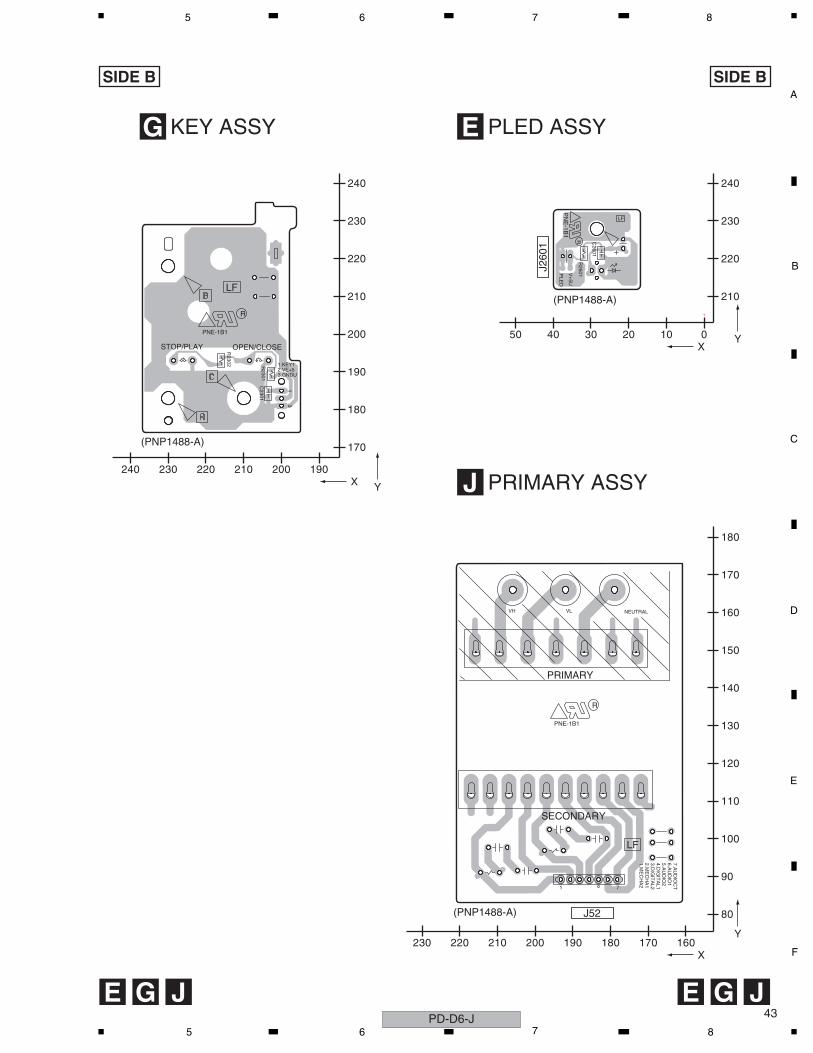
C
D
F
A
B
E
43
5 6 7 8
01020304050
210
220
230
240
XY
190200210220230240
170
180
190
200
210
220
230
240
X Y
160170180190200210220230
80
90
100
110
120
130
140
150
160
170
180
X
Y
R
LF
V+
5U
PLE
DP
NE
-1B1
C2601
R2601
LF
13
R
1.KEY12.VE+53.GNDU
OPEN/CLOSESTOP/PLAY
PNE-1B1
C2301
R2301
R2302
1 7
R
LF
VH VL NEUTRAL
7.AU
DIO
CT
6.AU
DIO
15.A
UD
IO2
4.DIG
ITA
L13.D
IGIT
AL2
2.ME
CH
A1
1.ME
CH
A2
PRIMARY
SECONDARY
PNE-1B1
J260
1
J52
SIDE B
E G J E G J
SIDE B
PLED ASSYE
PRIMARY ASSYJ
KEY ASSYG
(PNP1488-A)
(PNP1488-A)
(PNP1488-A)
PD-D6-J5 6 7 8
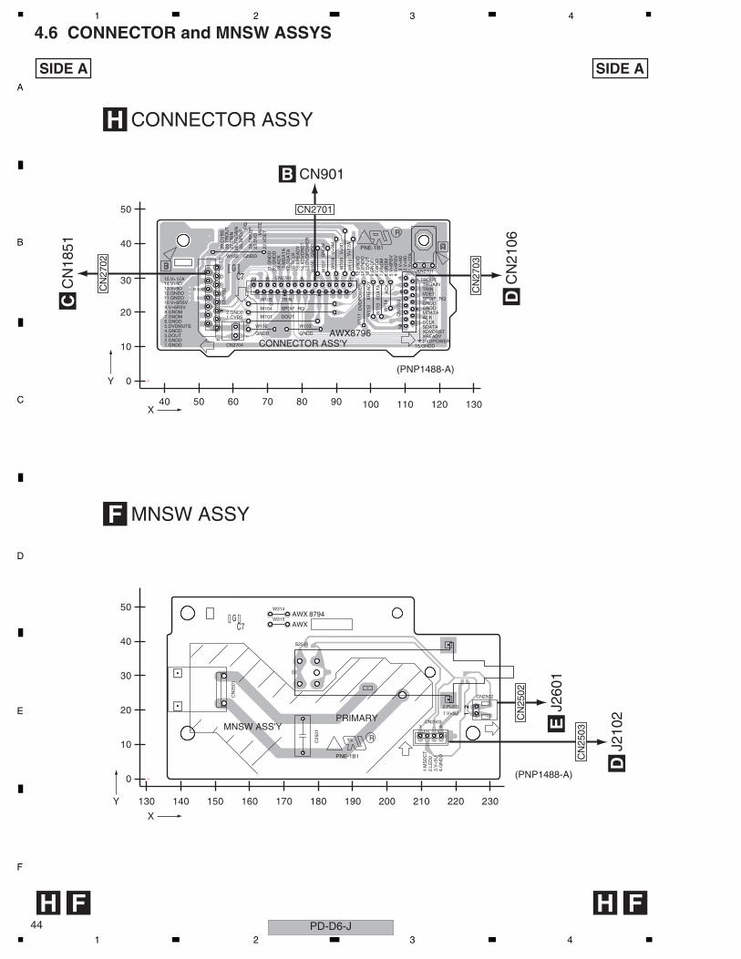
C
D
F
A
B
E
PD-D6-J44
1 2 3 4
4.6 CONNECTOR and MNSW ASSYS
40 50 60 70 80 90 100 110 120 130
0
10
20
30
40
50
X
Y
130 140 150 160 170 180 190 200 210 220 230
0
10
20
30
40
50
X
Y
11
5
GNDD GNDD
GN
DD
GN
DM
V+
9M
V+
9D
V+
12A
15
1
129
CONNECTOR ASS'YAWX8796
2.GNDD1.CVBS
[[ G ]]C7
R
14.V+9D15.V+12A
13.V+9D12.GNDD11.GNDD
8.GNDM7.GNDM
10.V+6R5V9.V+6R5V
6.GNDD5.DVDMUTE4.GNDD
2.GNDD3.DOUT
1.GNDD
1.TROUTTRGAINTRINVDETSPDIF_RQGNDDGNDDMDATAACKSCLKSDATAXDVDRSTXREADYDVDPOWER
15.GNDD
29.C
VB
S28
.TR
OU
T
26.T
RG
AIN
27.T
RIN
22.V
DE
T_RQ
21.G
ND
D20
.GN
DD
18.M
DA
TA
19.A
CK
16.S
CLK
17.S
DA
TA
14.X
DV
DR
ST
15.X
RE
AD
Y
13.D
VD
PO
WE
R
9.G
ND
D
12.G
ND
D
10.D
OU
T11
.GN
DD
MU
TE
8.G
ND
D
6.G
ND
M7.
GN
DM
5.V
+6R
5V4.
V+
6R5V
3.V
+9D
2.V
+9D
1.V
+12
A
24.T
RK
UP
GNDD
12
PNE-1B125.S
PD
IF
23.D
VD
DV
DP
OW
ER
XR
EA
DY
SD
AT
A
AC
K
TRIN
SPDIF_RQ
DOUT CN
2703C
N27
02
CN2701
W11
3
W11
4
W101
W132
W10
9
W11
0
W104
W105
W10
7W102
W10
6
W103 W11
1 W11
2
W10
8
CN2704
KN2701
MNSW ASS'Y
AWX
AWX
8794[[ G ]]C7
12
1
41
R
1.V+5U2.PLED
1.M
SD
CT
2
2.LE
D2
3.V
+5U
4.G
ND
DPNE-1B1
PRIMARY
W314
W315
C25
01
CN
2501
CN2502
CN2503
S2501
SIDE A SIDE A
H F H F
CN
1851
C
CN
2702
CN901B
CN2701
CN
2106
DCN
2703
J260
1EC
N25
02
J210
2DC
N25
03
CONNECTOR ASSYH
MNSW ASSYF
(PNP1488-A)
(PNP1488-A)
1 2 3 4
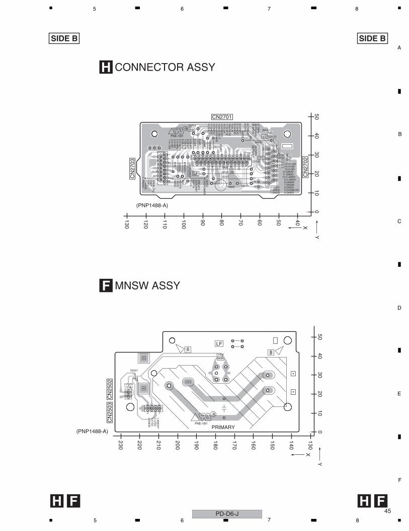
C
D
F
A
B
E
45
5 6 7 8
130
140
150
160
170
180
190
200
210
220
230
010
2030
4050
X
Y
405060708090100
110
120
130
010
2030
4050
X
Y
LF
14 R
1.V+5U
3.V+
5U
2.PLED
4.GN
DD
2.LED
21.M
SD
CT PRIMARY
PNE-1B1
C2502
Q2501
115
15
1
1 29
LF
R
12GN
DD
MD
AT
AA
CK
SC
LK
V+
12A
V+
9D
V+
9M
GN
DM
GN
DD
GNDD
GNDDGNDD
TR
OU
TT
RG
AIN
VD
ET
TR
IN
SP
DIF
_RQ
GN
DD
5.DVDMUTE
14.V+9D15.V+12A
12.GNDD13.V+9D
11.GNDD10.V+6R5V
9.V+6R5V8.GNDM7.GNDM6.GNDD
4.GNDD
3.DOUT2.GNDD1.GNDD
29.CV
BS
28.TR
OU
T
27.TR
IN26.T
RG
AIN
25.SP
DIF
24.TR
KU
P
MU
TE
22.VD
ET
21.GN
DD
20.GN
DD
19.AC
K18.M
DA
TA
17.SD
AT
A16.S
CLK
15.XR
EA
DY
14.XD
VD
RS
T13.D
VD
PO
WE
R12.G
ND
D11.G
ND
D10.D
OU
T
9.GN
DD
8.GN
DD
7.GN
DM
6.GN
DM
5.V+
6R5V
4.V+
6R5V
3.V+
9D2.V
+9D
1.V+
12A
SD
AT
AX
DV
DR
ST
XR
EA
DY
DV
DP
OW
ER
GN
DD
1.
15.
PNE-1B1
_RQ
23.DV
D
SPDIF_RQ
TRIN
DOUT
DV
DP
OW
ER
XR
EA
DY
SD
AT
A
AC
K
R2701
C2705
R2702C2701
C2702
C2703
C2704
H F H F
SIDE BSIDE B
CN
2702
CN2701
CN
2703
CN
2502
CN
2503
CONNECTOR ASSYH
MNSW ASSYF
(PNP1488-A)
(PNP1488-A)
PD-D6-J5 6 7 8
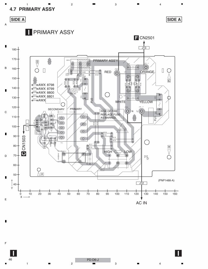
C
D
F
A
B
E
PD-D6-J46
1 2 3 4
4.7 PRIMARY ASSY
0 10 20 30 40 50 60 70 80 90 100 110 120 130 140 150 160
40
50
60
70
80
90
100
110
120
130
140
150
160
170
180
X
Y
41
3 1
HIGH LOW
AWX 8798AWX 8799AWX 8800
8801AWXAWX
PRIMARY ASS'Y
ORANGERED
[[ G ]]C7
R
J12-2 -1
SECONDARY PRIMARYRISK OF FIRE REPLACE FUSEAS MARKED.
FU
1
FU
2
YELLOWWHITE
GN
DU
J13-2
-1
3.V
L2.
VH
1.N
EU
TR
AL
1.SYSPOW2.AC3.V+5.6ST4.GNDU
NJM
78M
56F
A
PNE-1B1
exceptRLF model
RLF model
C16
IC11
D11
L11
RY11
S11
T11
J11
C15
CN13
W12
6
R12
C13
C12
C11
R13
W12
8
W12
7
W12
5W307
W308
W309
W310
W311
J12
J13
W12
1
W115
W134W
130
W12
9
H11
H12H
13
W12
3
W119
W116
W120
H14
W135
W12
2
W117
W12
4
W13
111
12
13
W118
LN
SIDE A
I
SIDE A
I
PRIMARY ASSYI
(PNP1488-A)
CN2501F
J13
J11
CN
1503
C
AC IN
J12
1 2 3 4
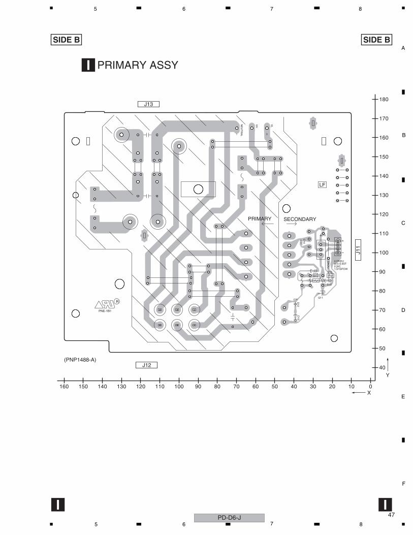
C
D
F
A
B
E
47
5 6 7 8
0102030405060708090100110120130140150160
40
50
60
70
80
90
100
110
120
130
140
150
160
170
180
X
Y
41
1 3
R
LF
SECONDARYPRIMARY
GN
DU
VL
VH
NE
UT
RA
L
4.GNDU3.V+5.6ST2.]AC1.SYSPOW
PNE-1B1
C14
Q11
D12
D13
D14
D15
R14
R15
SIDE B
I
SIDE B
I
PRIMARY ASSYI
(PNP1488-A)
J13
J11
J12
PD-D6-J5 6 7 8
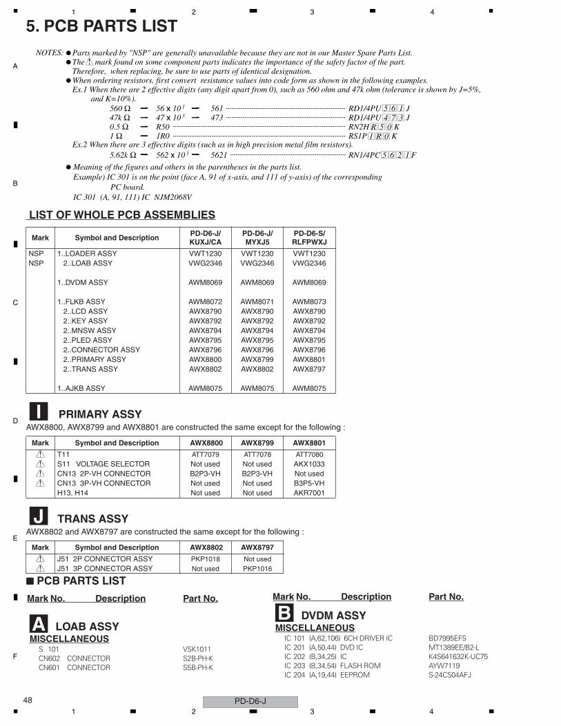
C
D
F
A
B
E
PD-D6-J48
1 2 3 4
5. PCB PARTS LIST
LIST OF WHOLE PCB ASSEMBLIES
AWX8800, AWX8799 and AWX8801 are constructed the same except for the following :
AWX8802 and AWX8797 are constructed the same except for the following :
7777 PCB PARTS LIST
Parts marked by "NSP" are generally unavailable because they are not in our Master Spare Parts List.The mark found on some component parts indicates the importance of the safety factor of the part.Therefore, when replacing, be sure to use parts of identical designation.When ordering resistors, first convert resistance values into code form as shown in the following examples.Ex.1 When there are 2 effective digits (any digit apart from 0), such as 560 ohm and 47k ohm (tolerance is shown by J=5%, and K=10%).
Ex.2 When there are 3 effective digits (such as in high precision metal film resistors).
5 6 14 7 3
R 5 01 R 0
5 6 2 1
NOTES:
560 Ω47k Ω0.5 Ω1 Ω
RD1/4PU JRD1/4PU JRN2H KRS1P K
56 x 10 1
47 x 10 3
R501R0
561473
5.62k Ω RN1/4PC F562 x 10 1 5621
Meaning of the figures and others in the parentheses in the parts list.Example) IC 301 is on the point (face A, 91 of x-axis, and 111 of y-axis) of the corresponding PC board.IC 301 (A, 91, 111) IC NJM2068V
Mark Symbol and Description PD-D6-J/ KUXJ/CA
PD-D6-J/ MYXJ5
PD-D6-S/ RLFPWXJ
NSP 1..LOADER ASSY VWT1230 VWT1230 VWT1230NSP 2..LOAB ASSY VWG2346 VWG2346 VWG2346
1..DVDM ASSY AWM8069 AWM8069 AWM8069
1..FLKB ASSY AWM8072 AWM8071 AWM8073 2..LCD ASSY AWX8790 AWX8790 AWX8790 2..KEY ASSY AWX8792 AWX8792 AWX8792 2..MNSW ASSY AWX8794 AWX8794 AWX8794 2..PLED ASSY AWX8795 AWX8795 AWX8795 2..CONNECTOR ASSY AWX8796 AWX8796 AWX8796 2..PRIMARY ASSY AWX8800 AWX8799 AWX8801 2..TRANS ASSY AWX8802 AWX8802 AWX8797
1..AJKB ASSY AWM8075 AWM8075 AWM8075
I PRIMARY ASSY
Mark Symbol and Description AWX8800 AWX8799 AWX8801
> T11 ATT7079 ATT7078 ATT7080> S11 VOLTAGE SELECTOR Not used Not used AKX1033> CN13 2P-VH CONNECTOR B2P3-VH B2P3-VH Not used> CN13 3P-VH CONNECTOR Not used Not used B3P5-VH
H13, H14 Not used Not used AKR7001
J TRANS ASSY
Mark Symbol and Description AWX8802 AWX8797
> J51 2P CONNECTOR ASSY PKP1018 Not used> J51 3P CONNECTOR ASSY Not used PKP1016
Mark No. Description Part No.
A LOAB ASSYMISCELLANEOUS
S 101 VSK1011CN602 CONNECTOR S2B-PH-KCN601 CONNECTOR S5B-PH-K
B DVDM ASSYMISCELLANEOUS
IC 101 (A,62,106) 6CH DRIVER IC BD7995EFSIC 201 (A,50,44) DVD IC MT1389EE/B2-LIC 202 (B,34,25) IC K4S641632K-UC75IC 203 (B,34,54) FLASH ROM AYW7119IC 204 (A,19,44) EEPROM S-24CS04AFJ
Mark No. Description Part No.
1 2 3 4
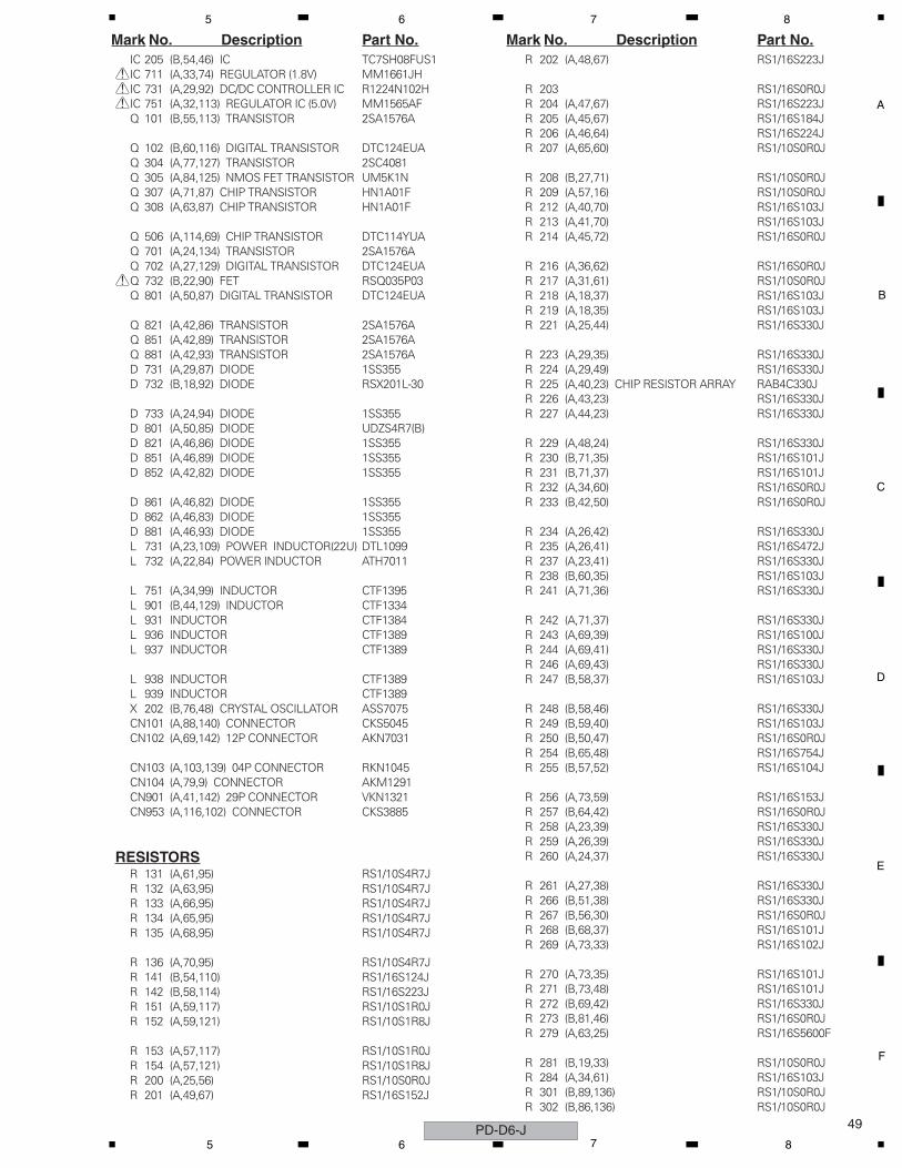
C
D
F
A
B
E
49
5 6 7 8
IC 205 (B,54,46) IC TC7SH08FUS1>IC 711 (A,33,74) REGULATOR (1.8V) MM1661JH>IC 731 (A,29,92) DC/DC CONTROLLER IC R1224N102H>IC 751 (A,32,113) REGULATOR IC (5.0V) MM1565AF
Q 101 (B,55,113) TRANSISTOR 2SA1576A
Q 102 (B,60,116) DIGITAL TRANSISTOR DTC124EUAQ 304 (A,77,127) TRANSISTOR 2SC4081Q 305 (A,84,125) NMOS FET TRANSISTOR UM5K1NQ 307 (A,71,87) CHIP TRANSISTOR HN1A01FQ 308 (A,63,87) CHIP TRANSISTOR HN1A01F
Q 506 (A,114,69) CHIP TRANSISTOR DTC114YUAQ 701 (A,24,134) TRANSISTOR 2SA1576AQ 702 (A,27,129) DIGITAL TRANSISTOR DTC124EUA
>Q 732 (B,22,90) FET RSQ035P03Q 801 (A,50,87) DIGITAL TRANSISTOR DTC124EUA
Q 821 (A,42,86) TRANSISTOR 2SA1576AQ 851 (A,42,89) TRANSISTOR 2SA1576AQ 881 (A,42,93) TRANSISTOR 2SA1576AD 731 (A,29,87) DIODE 1SS355D 732 (B,18,92) DIODE RSX201L-30
D 733 (A,24,94) DIODE 1SS355D 801 (A,50,85) DIODE UDZS4R7(B)D 821 (A,46,86) DIODE 1SS355D 851 (A,46,89) DIODE 1SS355D 852 (A,42,82) DIODE 1SS355
D 861 (A,46,82) DIODE 1SS355D 862 (A,46,83) DIODE 1SS355D 881 (A,46,93) DIODE 1SS355L 731 (A,23,109) POWER INDUCTOR(22U) DTL1099L 732 (A,22,84) POWER INDUCTOR ATH7011
L 751 (A,34,99) INDUCTOR CTF1395L 901 (B,44,129) INDUCTOR CTF1334L 931 INDUCTOR CTF1384L 936 INDUCTOR CTF1389L 937 INDUCTOR CTF1389
L 938 INDUCTOR CTF1389L 939 INDUCTOR CTF1389X 202 (B,76,48) CRYSTAL OSCILLATOR ASS7075CN101 (A,88,140) CONNECTOR CKS5045CN102 (A,69,142) 12P CONNECTOR AKN7031
CN103 (A,103,139) 04P CONNECTOR RKN1045CN104 (A,79,9) CONNECTOR AKM1291CN901 (A,41,142) 29P CONNECTOR VKN1321CN953 (A,116,102) CONNECTOR CKS3885
RESISTORSR 131 (A,61,95) RS1/10S4R7JR 132 (A,63,95) RS1/10S4R7JR 133 (A,66,95) RS1/10S4R7JR 134 (A,65,95) RS1/10S4R7JR 135 (A,68,95) RS1/10S4R7J
R 136 (A,70,95) RS1/10S4R7JR 141 (B,54,110) RS1/16S124JR 142 (B,58,114) RS1/16S223JR 151 (A,59,117) RS1/10S1R0JR 152 (A,59,121) RS1/10S1R8J
R 153 (A,57,117) RS1/10S1R0JR 154 (A,57,121) RS1/10S1R8JR 200 (A,25,56) RS1/10S0R0JR 201 (A,49,67) RS1/16S152J
Mark No. Description Part No.R 202 (A,48,67) RS1/16S223J
R 203 RS1/16S0R0JR 204 (A,47,67) RS1/16S223JR 205 (A,45,67) RS1/16S184JR 206 (A,46,64) RS1/16S224JR 207 (A,65,60) RS1/10S0R0J
R 208 (B,27,71) RS1/10S0R0JR 209 (A,57,16) RS1/10S0R0JR 212 (A,40,70) RS1/16S103JR 213 (A,41,70) RS1/16S103JR 214 (A,45,72) RS1/16S0R0J
R 216 (A,36,62) RS1/16S0R0JR 217 (A,31,61) RS1/10S0R0JR 218 (A,18,37) RS1/16S103JR 219 (A,18,35) RS1/16S103JR 221 (A,25,44) RS1/16S330J
R 223 (A,29,35) RS1/16S330JR 224 (A,29,49) RS1/16S330JR 225 (A,40,23) CHIP RESISTOR ARRAY RAB4C330JR 226 (A,43,23) RS1/16S330JR 227 (A,44,23) RS1/16S330J
R 229 (A,48,24) RS1/16S330JR 230 (B,71,35) RS1/16S101JR 231 (B,71,37) RS1/16S101JR 232 (A,34,60) RS1/16S0R0JR 233 (B,42,50) RS1/16S0R0J
R 234 (A,26,42) RS1/16S330JR 235 (A,26,41) RS1/16S472JR 237 (A,23,41) RS1/16S330JR 238 (B,60,35) RS1/16S103JR 241 (A,71,36) RS1/16S330J
R 242 (A,71,37) RS1/16S330JR 243 (A,69,39) RS1/16S100JR 244 (A,69,41) RS1/16S330JR 246 (A,69,43) RS1/16S330JR 247 (B,58,37) RS1/16S103J
R 248 (B,58,46) RS1/16S330JR 249 (B,59,40) RS1/16S103JR 250 (B,50,47) RS1/16S0R0JR 254 (B,65,48) RS1/16S754JR 255 (B,57,52) RS1/16S104J
R 256 (A,73,59) RS1/16S153JR 257 (B,64,42) RS1/16S0R0JR 258 (A,23,39) RS1/16S330JR 259 (A,26,39) RS1/16S330JR 260 (A,24,37) RS1/16S330J
R 261 (A,27,38) RS1/16S330JR 266 (B,51,38) RS1/16S330JR 267 (B,56,30) RS1/16S0R0JR 268 (B,68,37) RS1/16S101JR 269 (A,73,33) RS1/16S102J
R 270 (A,73,35) RS1/16S101JR 271 (B,73,48) RS1/16S101JR 272 (B,69,42) RS1/16S330JR 273 (B,81,46) RS1/16S0R0JR 279 (A,63,25) RS1/16S5600F
R 281 (B,19,33) RS1/10S0R0JR 284 (A,34,61) RS1/16S103JR 301 (B,89,136) RS1/10S0R0JR 302 (B,86,136) RS1/10S0R0J
Mark No. Description Part No.
PD-D6-J5 6 7 8
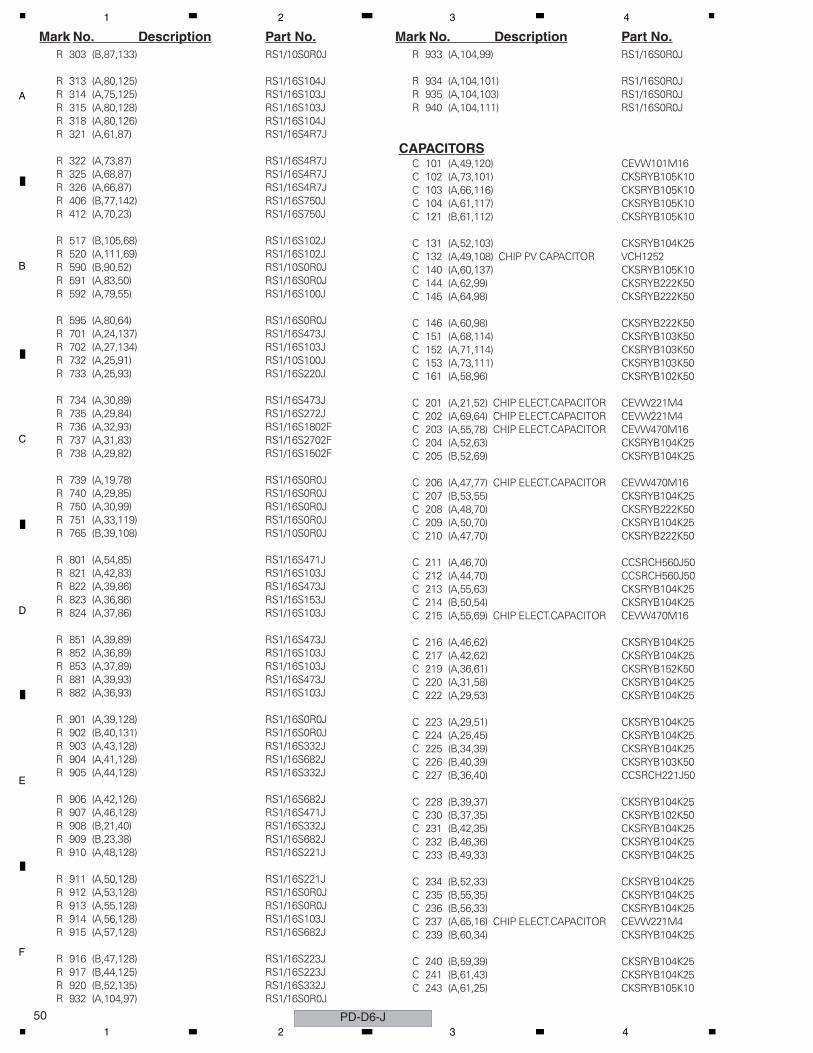
C
D
F
A
B
E
PD-D6-J50
1 2 3 4
R 303 (B,87,133) RS1/10S0R0J
R 313 (A,80,125) RS1/16S104JR 314 (A,75,125) RS1/16S103JR 315 (A,80,128) RS1/16S103JR 318 (A,80,126) RS1/16S104JR 321 (A,61,87) RS1/16S4R7J
R 322 (A,73,87) RS1/16S4R7JR 325 (A,68,87) RS1/16S4R7JR 326 (A,66,87) RS1/16S4R7JR 406 (B,77,142) RS1/16S750JR 412 (A,70,23) RS1/16S750J
R 517 (B,105,68) RS1/16S102JR 520 (A,111,69) RS1/16S102JR 590 (B,90,52) RS1/10S0R0JR 591 (A,83,50) RS1/16S0R0JR 592 (A,79,55) RS1/16S100J
R 595 (A,80,64) RS1/16S0R0JR 701 (A,24,137) RS1/16S473JR 702 (A,27,134) RS1/16S103JR 732 (A,25,91) RS1/10S100JR 733 (A,25,93) RS1/16S220J
R 734 (A,30,89) RS1/16S473JR 735 (A,29,84) RS1/16S272JR 736 (A,32,93) RS1/16S1802FR 737 (A,31,83) RS1/16S2702FR 738 (A,29,82) RS1/16S1502F
R 739 (A,19,78) RS1/16S0R0JR 740 (A,29,85) RS1/16S0R0JR 750 (A,30,99) RS1/16S0R0JR 751 (A,33,119) RS1/16S0R0JR 765 (B,39,108) RS1/10S0R0J
R 801 (A,54,85) RS1/16S471JR 821 (A,42,83) RS1/16S103JR 822 (A,39,86) RS1/16S473JR 823 (A,36,86) RS1/16S153JR 824 (A,37,86) RS1/16S103J
R 851 (A,39,89) RS1/16S473JR 852 (A,36,89) RS1/16S103JR 853 (A,37,89) RS1/16S103JR 881 (A,39,93) RS1/16S473JR 882 (A,36,93) RS1/16S103J
R 901 (A,39,128) RS1/16S0R0JR 902 (B,40,131) RS1/16S0R0JR 903 (A,43,128) RS1/16S332JR 904 (A,41,128) RS1/16S682JR 905 (A,44,128) RS1/16S332J
R 906 (A,42,126) RS1/16S682JR 907 (A,46,128) RS1/16S471JR 908 (B,21,40) RS1/16S332JR 909 (B,23,38) RS1/16S682JR 910 (A,48,128) RS1/16S221J
R 911 (A,50,128) RS1/16S221JR 912 (A,53,128) RS1/16S0R0JR 913 (A,55,128) RS1/16S0R0JR 914 (A,56,128) RS1/16S103JR 915 (A,57,128) RS1/16S682J
R 916 (B,47,128) RS1/16S223JR 917 (B,44,125) RS1/16S223JR 920 (B,52,135) RS1/16S332JR 932 (A,104,97) RS1/16S0R0J
Mark No. Description Part No.R 933 (A,104,99) RS1/16S0R0J
R 934 (A,104,101) RS1/16S0R0JR 935 (A,104,103) RS1/16S0R0JR 940 (A,104,111) RS1/16S0R0J
CAPACITORSC 101 (A,49,120) CEVW101M16C 102 (A,73,101) CKSRYB105K10C 103 (A,66,116) CKSRYB105K10C 104 (A,61,117) CKSRYB105K10C 121 (B,61,112) CKSRYB105K10
C 131 (A,52,103) CKSRYB104K25C 132 (A,49,108) CHIP PV CAPACITOR VCH1252C 140 (A,60,137) CKSRYB105K10C 144 (A,62,99) CKSRYB222K50C 145 (A,64,98) CKSRYB222K50
C 146 (A,60,98) CKSRYB222K50C 151 (A,68,114) CKSRYB103K50C 152 (A,71,114) CKSRYB103K50C 153 (A,73,111) CKSRYB103K50C 161 (A,58,96) CKSRYB102K50
C 201 (A,21,52) CHIP ELECT.CAPACITOR CEVW221M4C 202 (A,69,64) CHIP ELECT.CAPACITOR CEVW221M4C 203 (A,55,78) CHIP ELECT.CAPACITOR CEVW470M16C 204 (A,52,63) CKSRYB104K25C 205 (B,52,69) CKSRYB104K25
C 206 (A,47,77) CHIP ELECT.CAPACITOR CEVW470M16C 207 (B,53,55) CKSRYB104K25C 208 (A,48,70) CKSRYB222K50C 209 (A,50,70) CKSRYB104K25C 210 (A,47,70) CKSRYB222K50
C 211 (A,46,70) CCSRCH560J50C 212 (A,44,70) CCSRCH560J50C 213 (A,55,63) CKSRYB104K25C 214 (B,50,54) CKSRYB104K25C 215 (A,55,69) CHIP ELECT.CAPACITOR CEVW470M16
C 216 (A,46,62) CKSRYB104K25C 217 (A,42,62) CKSRYB104K25C 219 (A,36,61) CKSRYB152K50C 220 (A,31,58) CKSRYB104K25C 222 (A,29,53) CKSRYB104K25
C 223 (A,29,51) CKSRYB104K25C 224 (A,25,45) CKSRYB104K25C 225 (B,34,39) CKSRYB104K25C 226 (B,40,39) CKSRYB103K50C 227 (B,36,40) CCSRCH221J50
C 228 (B,39,37) CKSRYB104K25C 230 (B,37,35) CKSRYB102K50C 231 (B,42,35) CKSRYB104K25C 232 (B,46,36) CKSRYB104K25C 233 (B,49,33) CKSRYB104K25
C 234 (B,52,33) CKSRYB104K25C 235 (B,55,35) CKSRYB104K25C 236 (B,56,33) CKSRYB104K25C 237 (A,65,16) CHIP ELECT.CAPACITOR CEVW221M4C 239 (B,60,34) CKSRYB104K25
C 240 (B,59,39) CKSRYB104K25C 241 (B,61,43) CKSRYB104K25C 243 (A,61,25) CKSRYB105K10
Mark No. Description Part No.
1 2 3 4
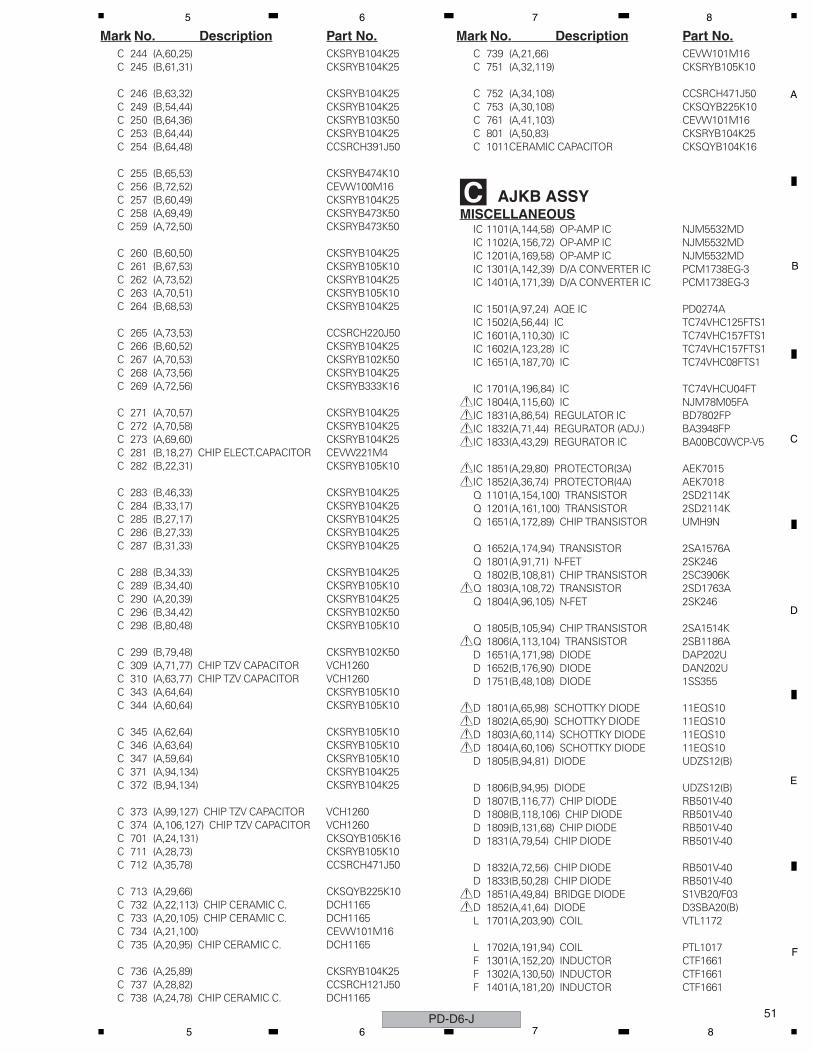
C
D
F
A
B
E
51
5 6 7 8
C 244 (A,60,25) CKSRYB104K25C 245 (B,61,31) CKSRYB104K25
C 246 (B,63,32) CKSRYB104K25C 249 (B,54,44) CKSRYB104K25C 250 (B,64,36) CKSRYB103K50C 253 (B,64,44) CKSRYB104K25C 254 (B,64,48) CCSRCH391J50
C 255 (B,65,53) CKSRYB474K10C 256 (B,72,52) CEVW100M16C 257 (B,60,49) CKSRYB104K25C 258 (A,69,49) CKSRYB473K50C 259 (A,72,50) CKSRYB473K50
C 260 (B,60,50) CKSRYB104K25C 261 (B,67,53) CKSRYB105K10C 262 (A,73,52) CKSRYB104K25C 263 (A,70,51) CKSRYB105K10C 264 (B,68,53) CKSRYB104K25
C 265 (A,73,53) CCSRCH220J50C 266 (B,60,52) CKSRYB104K25C 267 (A,70,53) CKSRYB102K50C 268 (A,73,56) CKSRYB104K25C 269 (A,72,56) CKSRYB333K16
C 271 (A,70,57) CKSRYB104K25C 272 (A,70,58) CKSRYB104K25C 273 (A,69,60) CKSRYB104K25C 281 (B,18,27) CHIP ELECT.CAPACITOR CEVW221M4C 282 (B,22,31) CKSRYB105K10
C 283 (B,46,33) CKSRYB104K25C 284 (B,33,17) CKSRYB104K25C 285 (B,27,17) CKSRYB104K25C 286 (B,27,33) CKSRYB104K25C 287 (B,31,33) CKSRYB104K25
C 288 (B,34,33) CKSRYB104K25C 289 (B,34,40) CKSRYB105K10C 290 (A,20,39) CKSRYB104K25C 296 (B,34,42) CKSRYB102K50C 298 (B,80,48) CKSRYB105K10
C 299 (B,79,48) CKSRYB102K50C 309 (A,71,77) CHIP TZV CAPACITOR VCH1260C 310 (A,63,77) CHIP TZV CAPACITOR VCH1260C 343 (A,64,64) CKSRYB105K10C 344 (A,60,64) CKSRYB105K10
C 345 (A,62,64) CKSRYB105K10C 346 (A,63,64) CKSRYB105K10C 347 (A,59,64) CKSRYB105K10C 371 (A,94,134) CKSRYB104K25C 372 (B,94,134) CKSRYB104K25
C 373 (A,99,127) CHIP TZV CAPACITOR VCH1260C 374 (A,106,127) CHIP TZV CAPACITOR VCH1260C 701 (A,24,131) CKSQYB105K16C 711 (A,28,73) CKSRYB105K10C 712 (A,35,78) CCSRCH471J50
C 713 (A,29,66) CKSQYB225K10C 732 (A,22,113) CHIP CERAMIC C. DCH1165C 733 (A,20,105) CHIP CERAMIC C. DCH1165C 734 (A,21,100) CEVW101M16C 735 (A,20,95) CHIP CERAMIC C. DCH1165
C 736 (A,25,89) CKSRYB104K25C 737 (A,28,82) CCSRCH121J50C 738 (A,24,78) CHIP CERAMIC C. DCH1165
Mark No. Description Part No.C 739 (A,21,66) CEVW101M16C 751 (A,32,119) CKSRYB105K10
C 752 (A,34,108) CCSRCH471J50C 753 (A,30,108) CKSQYB225K10C 761 (A,41,103) CEVW101M16C 801 (A,50,83) CKSRYB104K25C 1011CERAMIC CAPACITOR CKSQYB104K16
C AJKB ASSYMISCELLANEOUS
IC 1101(A,144,58) OP-AMP IC NJM5532MDIC 1102(A,156,72) OP-AMP IC NJM5532MDIC 1201(A,169,58) OP-AMP IC NJM5532MDIC 1301(A,142,39) D/A CONVERTER IC PCM1738EG-3IC 1401(A,171,39) D/A CONVERTER IC PCM1738EG-3
IC 1501(A,97,24) AQE IC PD0274AIC 1502(A,56,44) IC TC74VHC125FTS1IC 1601(A,110,30) IC TC74VHC157FTS1IC 1602(A,123,28) IC TC74VHC157FTS1IC 1651(A,187,70) IC TC74VHC08FTS1
IC 1701(A,196,84) IC TC74VHCU04FT>IC 1804(A,115,60) IC NJM78M05FA>IC 1831(A,86,54) REGULATOR IC BD7802FP>IC 1832(A,71,44) REGURATOR (ADJ.) BA3948FP>IC 1833(A,43,29) REGURATOR IC BA00BC0WCP-V5
>IC 1851(A,29,80) PROTECTOR(3A) AEK7015>IC 1852(A,36,74) PROTECTOR(4A) AEK7018
Q 1101(A,154,100) TRANSISTOR 2SD2114KQ 1201(A,161,100) TRANSISTOR 2SD2114KQ 1651(A,172,89) CHIP TRANSISTOR UMH9N
Q 1652(A,174,94) TRANSISTOR 2SA1576AQ 1801(A,91,71) N-FET 2SK246Q 1802(B,108,81) CHIP TRANSISTOR 2SC3906K
>Q 1803(A,108,72) TRANSISTOR 2SD1763AQ 1804(A,96,105) N-FET 2SK246
Q 1805(B,105,94) CHIP TRANSISTOR 2SA1514K>Q 1806(A,113,104) TRANSISTOR 2SB1186A
D 1651(A,171,98) DIODE DAP202UD 1652(B,176,90) DIODE DAN202UD 1751(B,48,108) DIODE 1SS355
>D 1801(A,65,98) SCHOTTKY DIODE 11EQS10>D 1802(A,65,90) SCHOTTKY DIODE 11EQS10>D 1803(A,60,114) SCHOTTKY DIODE 11EQS10>D 1804(A,60,106) SCHOTTKY DIODE 11EQS10
D 1805(B,94,81) DIODE UDZS12(B)
D 1806(B,94,95) DIODE UDZS12(B)D 1807(B,116,77) CHIP DIODE RB501V-40D 1808(B,118,106) CHIP DIODE RB501V-40D 1809(B,131,68) CHIP DIODE RB501V-40D 1831(A,79,54) CHIP DIODE RB501V-40
D 1832(A,72,56) CHIP DIODE RB501V-40D 1833(B,50,28) CHIP DIODE RB501V-40
>D 1851(A,49,84) BRIDGE DIODE S1VB20/F03>D 1852(A,41,64) DIODE D3SBA20(B)
L 1701(A,203,90) COIL VTL1172
L 1702(A,191,94) COIL PTL1017F 1301(A,152,20) INDUCTOR CTF1661F 1302(A,130,50) INDUCTOR CTF1661F 1401(A,181,20) INDUCTOR CTF1661
Mark No. Description Part No.
PD-D6-J5 6 7 8
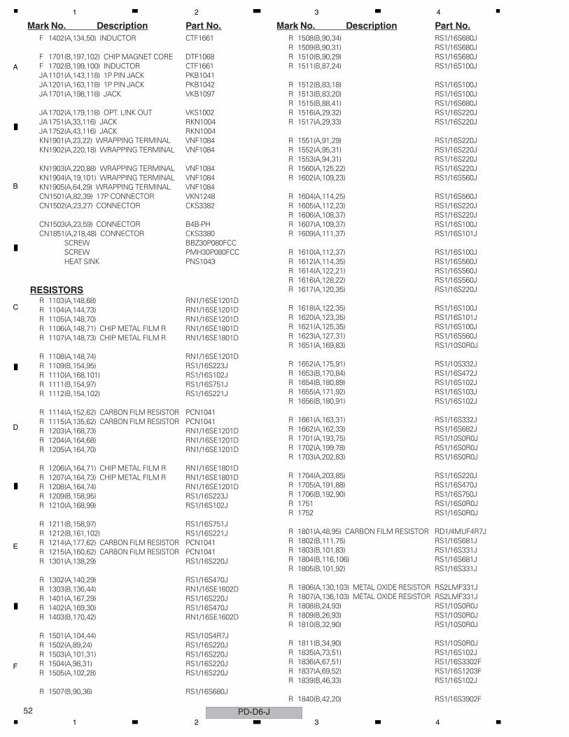
C
D
F
A
B
E
PD-D6-J52
1 2 3 4
F 1402(A,134,50) INDUCTOR CTF1661
F 1701(B,197,102) CHIP MAGNET CORE DTF1068F 1702(B,199,100) INDUCTOR CTF1661JA1101(A,143,118) 1P PIN JACK PKB1041JA1201(A,163,118) 1P PIN JACK PKB1042JA1701(A,198,118) JACK VKB1097
JA1702(A,179,118) OPT. LINK OUT VKS1002JA1751(A,33,116) JACK RKN1004JA1752(A,43,116) JACK RKN1004KN1901(A,23,22) WRAPPING TERMINAL VNF1084KN1902(A,220,18) WRAPPING TERMINAL VNF1084
KN1903(A,220,88) WRAPPING TERMINAL VNF1084KN1904(A,19,101) WRAPPING TERMINAL VNF1084KN1905(A,64,29) WRAPPING TERMINAL VNF1084CN1501(A,82,39) 17P CONNECTOR VKN1248CN1502(A,23,27) CONNECTOR CKS3382
CN1503(A,23,59) CONNECTOR B4B-PHCN1851(A,218,48) CONNECTOR CKS3380
SCREW BBZ30P080FCCSCREW PMH30P080FCCHEAT SINK PNS1043
RESISTORSR 1103(A,148,68) RN1/16SE1201DR 1104(A,144,73) RN1/16SE1201DR 1105(A,148,70) RN1/16SE1201DR 1106(A,148,71) CHIP METAL FILM R RN1/16SE1801DR 1107(A,148,73) CHIP METAL FILM R RN1/16SE1801D
R 1108(A,148,74) RN1/16SE1201DR 1109(B,154,95) RS1/16S223JR 1110(A,168,101) RS1/16S102JR 1111(B,154,97) RS1/16S751JR 1112(B,154,102) RS1/16S221J
R 1114(A,152,62) CARBON FILM RESISTOR PCN1041R 1115(A,135,62) CARBON FILM RESISTOR PCN1041R 1203(A,168,73) RN1/16SE1201DR 1204(A,164,68) RN1/16SE1201DR 1205(A,164,70) RN1/16SE1201D
R 1206(A,164,71) CHIP METAL FILM R RN1/16SE1801DR 1207(A,164,73) CHIP METAL FILM R RN1/16SE1801DR 1208(A,164,74) RN1/16SE1201DR 1209(B,158,95) RS1/16S223JR 1210(A,168,99) RS1/16S102J
R 1211(B,158,97) RS1/16S751JR 1212(B,161,102) RS1/16S221JR 1214(A,177,62) CARBON FILM RESISTOR PCN1041R 1215(A,160,62) CARBON FILM RESISTOR PCN1041R 1301(A,138,29) RS1/16S220J
R 1302(A,140,29) RS1/16S470JR 1303(B,136,44) RN1/16SE1602DR 1401(A,167,29) RS1/16S220JR 1402(A,169,30) RS1/16S470JR 1403(B,170,42) RN1/16SE1602D
R 1501(A,104,44) RS1/10S4R7JR 1502(A,89,24) RS1/16S220JR 1503(A,101,31) RS1/16S220JR 1504(A,98,31) RS1/16S220JR 1505(A,102,28) RS1/16S220J
R 1507(B,90,36) RS1/16S680J
Mark No. Description Part No.R 1508(B,90,34) RS1/16S680JR 1509(B,90,31) RS1/16S680JR 1510(B,90,29) RS1/16S680JR 1511(B,87,24) RS1/16S100J
R 1512(B,83,18) RS1/16S100JR 1513(B,83,20) RS1/16S100JR 1515(B,88,41) RS1/16S680JR 1516(A,29,32) RS1/16S220JR 1517(A,29,33) RS1/16S220J
R 1551(A,91,29) RS1/16S220JR 1552(A,95,31) RS1/16S220JR 1553(A,94,31) RS1/16S220JR 1560(A,125,22) RS1/16S220JR 1602(A,109,23) RS1/16S560J
R 1604(A,114,25) RS1/16S560JR 1605(A,112,23) RS1/16S220JR 1606(A,108,37) RS1/16S220JR 1607(A,109,37) RS1/16S100JR 1609(A,111,37) RS1/16S101J
R 1610(A,112,37) RS1/16S100JR 1612(A,114,35) RS1/16S560JR 1614(A,122,21) RS1/16S560JR 1616(A,128,22) RS1/16S560JR 1617(A,120,35) RS1/16S220J
R 1618(A,122,35) RS1/16S100JR 1620(A,123,35) RS1/16S101JR 1621(A,125,35) RS1/16S100JR 1623(A,127,31) RS1/16S560JR 1651(A,169,83) RS1/10S0R0J
R 1652(A,175,91) RS1/10S332JR 1653(B,170,84) RS1/16S472JR 1654(B,180,89) RS1/16S102JR 1655(A,171,92) RS1/16S103JR 1656(B,180,91) RS1/16S102J
R 1661(A,163,31) RS1/16S332JR 1662(A,162,33) RS1/16S682JR 1701(A,193,75) RS1/10S0R0JR 1702(A,199,78) RS1/16S0R0JR 1703(A,202,83) RS1/16S0R0J
R 1704(A,203,85) RS1/16S220JR 1705(A,191,88) RS1/16S470JR 1706(B,192,90) RS1/16S750JR 1751 RS1/16S0R0JR 1752 RS1/16S0R0J
R 1801(A,48,95) CARBON FILM RESISTOR RD1/4MUF4R7JR 1802(B,111,75) RS1/16S681JR 1803(B,101,83) RS1/16S331JR 1804(B,116,106) RS1/16S681JR 1805(B,101,92) RS1/16S331J
R 1806(A,130,103) METAL OXIDE RESISTOR RS2LMF331JR 1807(A,136,103) METAL OXIDE RESISTOR RS2LMF331JR 1808(B,24,93) RS1/10S0R0JR 1809(B,26,93) RS1/10S0R0JR 1810(B,32,90) RS1/10S0R0J
R 1811(B,34,90) RS1/10S0R0JR 1835(A,73,51) RS1/16S102JR 1836(A,67,51) RS1/16S3302FR 1837(A,69,52) RS1/16S1203FR 1839(B,46,33) RS1/16S102J
R 1840(B,42,20) RS1/16S3902F
Mark No. Description Part No.
1 2 3 4
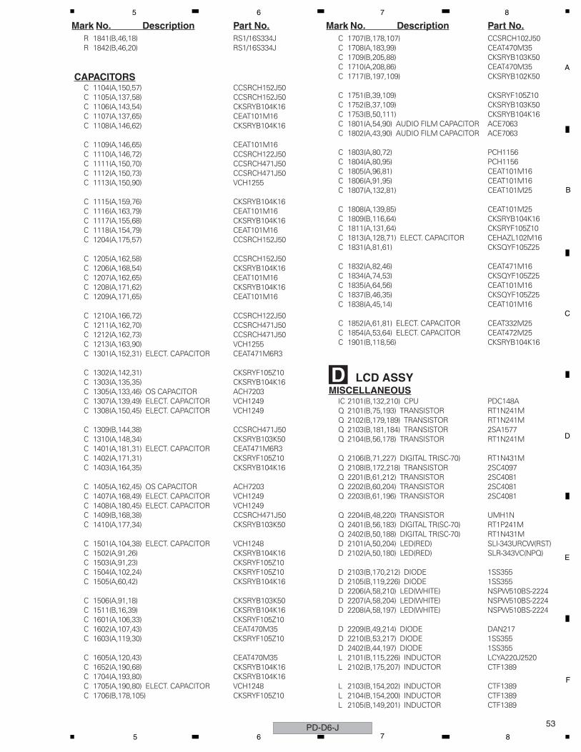
C
D
F
A
B
E
53
5 6 7 8
R 1841(B,46,18) RS1/16S334JR 1842(B,46,20) RS1/16S334J
CAPACITORSC 1104(A,150,57) CCSRCH152J50C 1105(A,137,58) CCSRCH152J50C 1106(A,143,54) CKSRYB104K16C 1107(A,137,65) CEAT101M16C 1108(A,146,62) CKSRYB104K16
C 1109(A,146,65) CEAT101M16C 1110(A,146,72) CCSRCH122J50C 1111(A,150,70) CCSRCH471J50C 1112(A,150,73) CCSRCH471J50C 1113(A,150,90) VCH1255
C 1115(A,159,76) CKSRYB104K16C 1116(A,163,79) CEAT101M16C 1117(A,155,68) CKSRYB104K16C 1118(A,154,79) CEAT101M16C 1204(A,175,57) CCSRCH152J50
C 1205(A,162,58) CCSRCH152J50C 1206(A,168,54) CKSRYB104K16C 1207(A,162,65) CEAT101M16C 1208(A,171,62) CKSRYB104K16C 1209(A,171,65) CEAT101M16
C 1210(A,166,72) CCSRCH122J50C 1211(A,162,70) CCSRCH471J50C 1212(A,162,73) CCSRCH471J50C 1213(A,163,90) VCH1255C 1301(A,152,31) ELECT. CAPACITOR CEAT471M6R3
C 1302(A,142,31) CKSRYF105Z10C 1303(A,135,35) CKSRYB104K16C 1305(A,133,46) OS CAPACITOR ACH7203C 1307(A,139,49) ELECT. CAPACITOR VCH1249C 1308(A,150,45) ELECT. CAPACITOR VCH1249
C 1309(B,144,38) CCSRCH471J50C 1310(A,148,34) CKSRYB103K50C 1401(A,181,31) ELECT. CAPACITOR CEAT471M6R3C 1402(A,171,31) CKSRYF105Z10C 1403(A,164,35) CKSRYB104K16
C 1405(A,162,45) OS CAPACITOR ACH7203C 1407(A,168,49) ELECT. CAPACITOR VCH1249C 1408(A,180,45) ELECT. CAPACITOR VCH1249C 1409(B,168,38) CCSRCH471J50C 1410(A,177,34) CKSRYB103K50
C 1501(A,104,38) ELECT. CAPACITOR VCH1248C 1502(A,91,26) CKSRYB104K16C 1503(A,91,23) CKSRYF105Z10C 1504(A,102,24) CKSRYF105Z10C 1505(A,60,42) CKSRYB104K16
C 1506(A,91,18) CKSRYB103K50C 1511(B,16,39) CKSRYB104K16C 1601(A,106,33) CKSRYF105Z10C 1602(A,107,43) CEAT470M35C 1603(A,119,30) CKSRYF105Z10
C 1605(A,120,43) CEAT470M35C 1652(A,190,68) CKSRYB104K16C 1704(A,193,80) CKSRYB104K16C 1705(A,190,80) ELECT. CAPACITOR VCH1248C 1706(B,178,105) CKSRYF105Z10
Mark No. Description Part No.C 1707(B,178,107) CCSRCH102J50C 1708(A,183,99) CEAT470M35C 1709(B,205,88) CKSRYB103K50C 1710(A,208,86) CEAT470M35C 1717(B,197,109) CKSRYB102K50
C 1751(B,39,109) CKSRYF105Z10C 1752(B,37,109) CKSRYB103K50C 1753(B,50,111) CKSRYB104K16C 1801(A,54,90) AUDIO FILM CAPACITOR ACE7063C 1802(A,43,90) AUDIO FILM CAPACITOR ACE7063
C 1803(A,80,72) PCH1156C 1804(A,80,95) PCH1156C 1805(A,96,81) CEAT101M16C 1806(A,91,95) CEAT101M16C 1807(A,132,81) CEAT101M25
C 1808(A,139,85) CEAT101M25C 1809(B,116,64) CKSRYB104K16C 1811(A,131,64) CKSRYF105Z10C 1813(A,128,71) ELECT. CAPACITOR CEHAZL102M16C 1831(A,81,61) CKSQYF105Z25
C 1832(A,82,46) CEAT471M16C 1834(A,74,53) CKSQYF105Z25C 1835(A,64,56) CEAT101M16C 1837(B,46,35) CKSQYF105Z25C 1838(A,45,14) CEAT101M16
C 1852(A,61,81) ELECT. CAPACITOR CEAT332M25C 1854(A,53,64) ELECT. CAPACITOR CEAT472M25C 1901(B,118,56) CKSRYB104K16
D LCD ASSYMISCELLANEOUS
IC 2101(B,132,210) CPU PDC148AQ 2101(B,75,193) TRANSISTOR RT1N241MQ 2102(B,179,189) TRANSISTOR RT1N241MQ 2103(B,181,184) TRANSISTOR 2SA1577Q 2104(B,56,178) TRANSISTOR RT1N241M
Q 2106(B,71,227) DIGITAL TR(SC-70) RT1N431MQ 2108(B,172,218) TRANSISTOR 2SC4097Q 2201(B,61,212) TRANSISTOR 2SC4081Q 2202(B,60,204) TRANSISTOR 2SC4081Q 2203(B,61,196) TRANSISTOR 2SC4081
Q 2204(B,48,220) TRANSISTOR UMH1NQ 2401(B,56,183) DIGITAL TR(SC-70) RT1P241MQ 2402(B,50,188) DIGITAL TR(SC-70) RT1N431MD 2101(A,50,204) LED(RED) SLI-343URCW(RST)D 2102(A,50,180) LED(RED) SLR-343VC(NPQ)
D 2103(B,170,212) DIODE 1SS355D 2105(B,119,226) DIODE 1SS355D 2206(A,58,210) LED(WHITE) NSPW510BS-2224D 2207(A,58,204) LED(WHITE) NSPW510BS-2224D 2208(A,58,197) LED(WHITE) NSPW510BS-2224
D 2209(B,49,214) DIODE DAN217D 2210(B,53,217) DIODE 1SS355D 2402(B,44,197) DIODE 1SS355L 2101(B,115,226) INDUCTOR LCYA220J2520L 2102(B,175,207) INDUCTOR CTF1389
L 2103(B,154,202) INDUCTOR CTF1389L 2104(B,154,200) INDUCTOR CTF1389L 2105(B,149,201) INDUCTOR CTF1389
Mark No. Description Part No.
PD-D6-J5 6 7 8
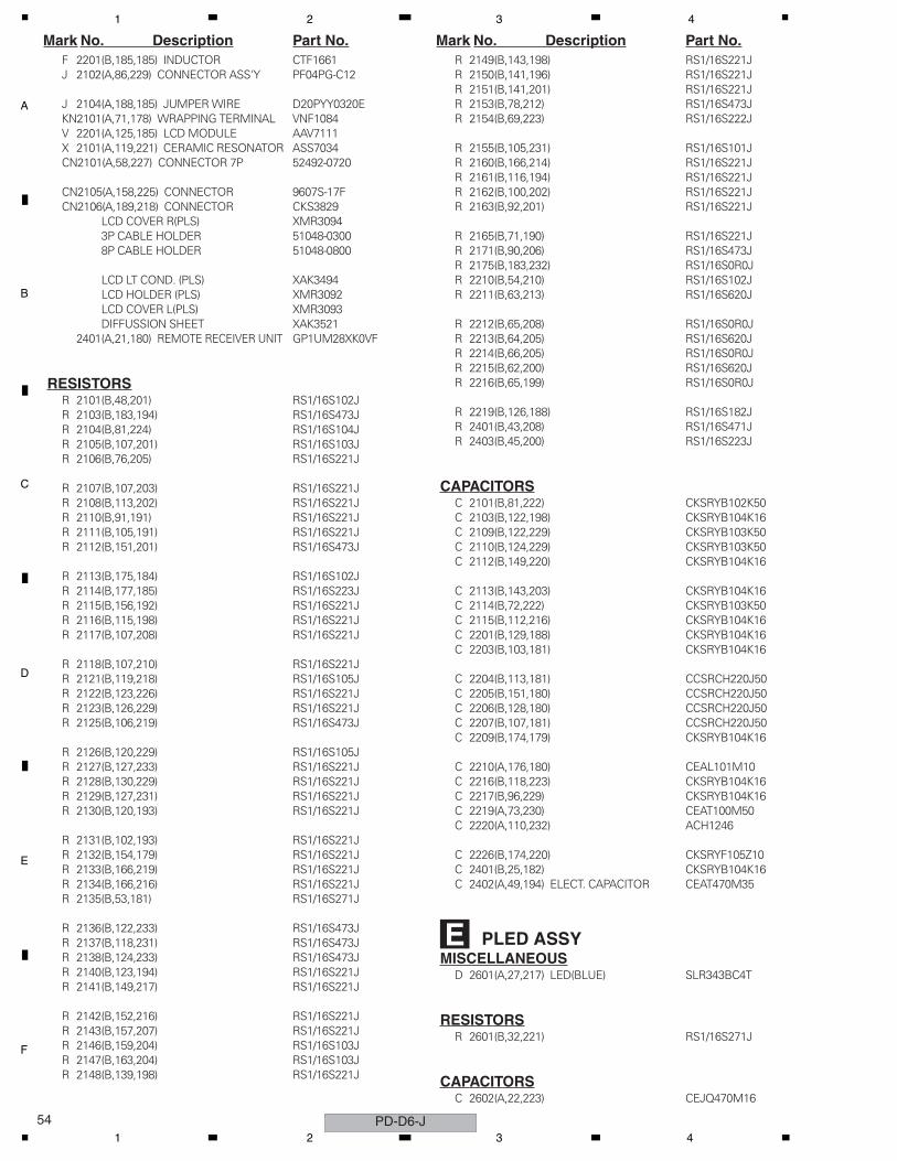
C
D
F
A
B
E
PD-D6-J54
1 2 3 4
F 2201(B,185,185) INDUCTOR CTF1661J 2102(A,86,229) CONNECTOR ASS'Y PF04PG-C12
J 2104(A,188,185) JUMPER WIRE D20PYY0320EKN2101(A,71,178) WRAPPING TERMINAL VNF1084V 2201(A,125,185) LCD MODULE AAV7111X 2101(A,119,221) CERAMIC RESONATOR ASS7034CN2101(A,58,227) CONNECTOR 7P 52492-0720
CN2105(A,158,225) CONNECTOR 9607S-17FCN2106(A,189,218) CONNECTOR CKS3829
LCD COVER R(PLS) XMR30943P CABLE HOLDER 51048-03008P CABLE HOLDER 51048-0800
LCD LT COND. (PLS) XAK3494LCD HOLDER (PLS) XMR3092LCD COVER L(PLS) XMR3093DIFFUSSION SHEET XAK3521
2401(A,21,180) REMOTE RECEIVER UNIT GP1UM28XK0VF
RESISTORSR 2101(B,48,201) RS1/16S102JR 2103(B,183,194) RS1/16S473JR 2104(B,81,224) RS1/16S104JR 2105(B,107,201) RS1/16S103JR 2106(B,76,205) RS1/16S221J
R 2107(B,107,203) RS1/16S221JR 2108(B,113,202) RS1/16S221JR 2110(B,91,191) RS1/16S221JR 2111(B,105,191) RS1/16S221JR 2112(B,151,201) RS1/16S473J
R 2113(B,175,184) RS1/16S102JR 2114(B,177,185) RS1/16S223JR 2115(B,156,192) RS1/16S221JR 2116(B,115,198) RS1/16S221JR 2117(B,107,208) RS1/16S221J
R 2118(B,107,210) RS1/16S221JR 2121(B,119,218) RS1/16S105JR 2122(B,123,226) RS1/16S221JR 2123(B,126,229) RS1/16S221JR 2125(B,106,219) RS1/16S473J
R 2126(B,120,229) RS1/16S105JR 2127(B,127,233) RS1/16S221JR 2128(B,130,229) RS1/16S221JR 2129(B,127,231) RS1/16S221JR 2130(B,120,193) RS1/16S221J
R 2131(B,102,193) RS1/16S221JR 2132(B,154,179) RS1/16S221JR 2133(B,166,219) RS1/16S221JR 2134(B,166,216) RS1/16S221JR 2135(B,53,181) RS1/16S271J
R 2136(B,122,233) RS1/16S473JR 2137(B,118,231) RS1/16S473JR 2138(B,124,233) RS1/16S473JR 2140(B,123,194) RS1/16S221JR 2141(B,149,217) RS1/16S221J
R 2142(B,152,216) RS1/16S221JR 2143(B,157,207) RS1/16S221JR 2146(B,159,204) RS1/16S103JR 2147(B,163,204) RS1/16S103JR 2148(B,139,198) RS1/16S221J
Mark No. Description Part No.R 2149(B,143,198) RS1/16S221JR 2150(B,141,196) RS1/16S221JR 2151(B,141,201) RS1/16S221JR 2153(B,78,212) RS1/16S473JR 2154(B,69,223) RS1/16S222J
R 2155(B,105,231) RS1/16S101JR 2160(B,166,214) RS1/16S221JR 2161(B,116,194) RS1/16S221JR 2162(B,100,202) RS1/16S221JR 2163(B,92,201) RS1/16S221J
R 2165(B,71,190) RS1/16S221JR 2171(B,90,206) RS1/16S473JR 2175(B,183,232) RS1/16S0R0JR 2210(B,54,210) RS1/16S102JR 2211(B,63,213) RS1/16S620J
R 2212(B,65,208) RS1/16S0R0JR 2213(B,64,205) RS1/16S620JR 2214(B,66,205) RS1/16S0R0JR 2215(B,62,200) RS1/16S620JR 2216(B,65,199) RS1/16S0R0J
R 2219(B,126,188) RS1/16S182JR 2401(B,43,208) RS1/16S471JR 2403(B,45,200) RS1/16S223J
CAPACITORSC 2101(B,81,222) CKSRYB102K50C 2103(B,122,198) CKSRYB104K16C 2109(B,122,229) CKSRYB103K50C 2110(B,124,229) CKSRYB103K50C 2112(B,149,220) CKSRYB104K16
C 2113(B,143,203) CKSRYB104K16C 2114(B,72,222) CKSRYB103K50C 2115(B,112,216) CKSRYB104K16C 2201(B,129,188) CKSRYB104K16C 2203(B,103,181) CKSRYB104K16
C 2204(B,113,181) CCSRCH220J50C 2205(B,151,180) CCSRCH220J50C 2206(B,128,180) CCSRCH220J50C 2207(B,107,181) CCSRCH220J50C 2209(B,174,179) CKSRYB104K16
C 2210(A,176,180) CEAL101M10C 2216(B,118,223) CKSRYB104K16C 2217(B,96,229) CKSRYB104K16C 2219(A,73,230) CEAT100M50C 2220(A,110,232) ACH1246
C 2226(B,174,220) CKSRYF105Z10C 2401(B,25,182) CKSRYB104K16C 2402(A,49,194) ELECT. CAPACITOR CEAT470M35
E PLED ASSYMISCELLANEOUS
D 2601(A,27,217) LED(BLUE) SLR343BC4T
RESISTORSR 2601(B,32,221) RS1/16S271J
CAPACITORSC 2602(A,22,223) CEJQ470M16
Mark No. Description Part No.
1 2 3 4
C
D
F
A
B
E
55
5 6 7 8
F MNSW ASSYMISCELLANEOUS
Q 2501(B,223,30) TRANSISTOR RT1N241M>S 2501(A,219,31) POWER SWITCH VSA1005>CN2501(A,153,22) AMP U-P CONNECTOR VKN2024
CN2502(A,226,19) CONNECTOR S2B-PHCN2503(A,210,13) CONNECTOR B4B-PH
G KEY ASSYMISCELLANEOUS
S 2301(A,204,193) SWITCH VSG1024S 2302(A,224,193) SWITCH VSG1024
2301(A,202,222) PCB BINDER VEF10403P CABLE HOLDER 51048-0300
RESISTORSR 2301(B,203,190) RS1/16S103JR 2302(B,216,193) RS1/16S103J
H CONECTOR ASSYMISCELLANEOUS
KN2701(A,113,34) WRAPPING TERMINAL VNF1084CN2701(A,94,28) CONNECTOR VKN1205CN2702(A,55,16) CONNECTOR CKS3380CN2703(A,110,30) CONNECTOR VKN1191CN2704(A,61,13) CONNECTOR B2P-SHF-1AA
CAPACITORSC 2701(B,49,24) CKSRYB104K16
I PRIMARY ASSY (KUXJ/CA type)MISCELLANEOUS>IC 11 (A,26,99) REGULATOR IC NJM78M56FA
Q 11 (B,26,79) TRANSISTOR RT1N241M>D 11 (A,32,99) BRIDGE DIODE S1VB20/F03
D 12 (B,39,73) DIODE 1SS355D 13 (B,39,65) DIODE 1SS355
D 14 (B,29,91) DIODE 1SS355D 15 (B,21,85) DIODE UDZS5R1(B)
>L 11 (A,122,137) LINE FILTER XTF3004H 11 (A,144,113) FUSE CLIP AKR7001H 12 (A,144,133) FUSE CLIP AKR7001
J 11 (A,17,100) CONNECTOR ASSY PF04PG-C07>J 12 (A,126,116) AC INLET ASSY PKP1014>J 13 (A,130,162) 2P CONECTOR ASSY PKP1015>RY11 (A,65,71) JOE LOWPOWER RELAY ASR7013>T 11 (A,65,110) POWER TRANSFORMER ATT7079
>CN13 (A,70,165) CONNECTOR B2P3-VH13 (A,118,109) PCB BINDER VEF104011 (A,15,148) PCB BINDER VEF104012 (A,30,168) PCB BINDER VEF1040
RESISTORSR 12 (A,32,88) CARBON FILM RESISTOR RD1/4MUF220JR 14 (B,29,85) RS1/16S332J
Mark No. Description Part No.R 15 (B,21,88) RS1/16S103J
CAPACITORS>C 12 (A,122,162) FILM CAPACITOR ACE7013
C 15 (A,25,88) ELECT. CAPACITOR CEAT102M25C 16 (A,25,110) CEAT221M16
J TRANS ASSY (KUXJ/CA type)MISCELLANEOUS>J 51 (A,192,166) 2P CONECTOR ASSY PKP1018
J 52 (A,193,89) 7P CONNECTOR ASSY PKP1017
RESISTORSR 51 (A,210,91) CARBON FILM RESISTOR RD1/4MUF4R7JR 52 (A,193,97) CARBON FILM RESISTOR RD1/4MUF4R7J
CAPACITORSC 51 (A,213,98) AUDIO FILM CAPACITOR ACE7060C 52 (A,205,92) AUDIO FILM CAPACITOR ACE7060C 53 (A,196,103) CFTLA824J50C 54 (A,186,100) CFTLA824J50
Mark No. Description Part No.
PD-D6-J5 6 7 8
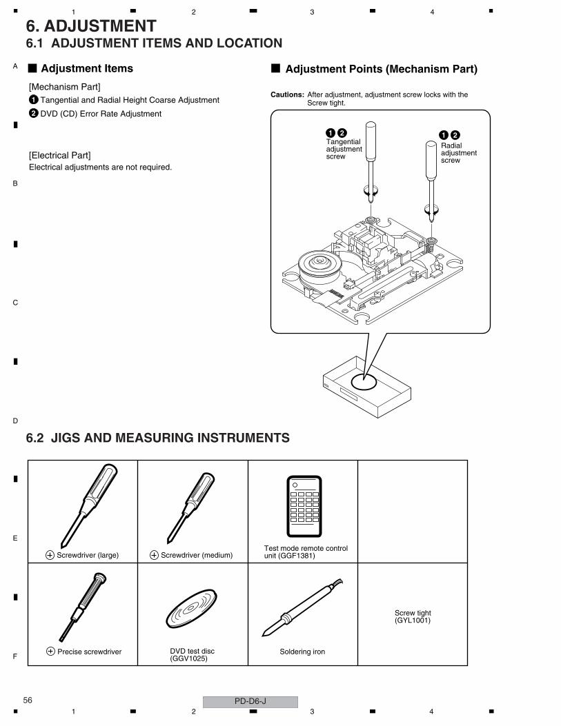
C
D
F
A
B
E
PD-D6-J56
1 2 3 4
6. ADJUSTMENT6.1 ADJUSTMENT ITEMS AND LOCATION
6.2 JIGS AND MEASURING INSTRUMENTS
1
2
Adjustment Items
[Mechanism Part]
[Electrical Part]
Tangential and Radial Height Coarse Adjustment
DVD (CD) Error Rate Adjustment
Electrical adjustments are not required.
Adjustment Points (Mechanism Part)
Cautions: After adjustment, adjustment screw locks with the Screw tight.
1 2Radialadjustmentscrew
1 2Tangentialadjustmentscrew
Screwdriver (large)
Precise screwdriver DVD test disc(GGV1025)
Test mode remote controlunit (GGF1381)
Screw tight(GYL1001)
Screwdriver (medium)
Soldering iron
1 2 3 4
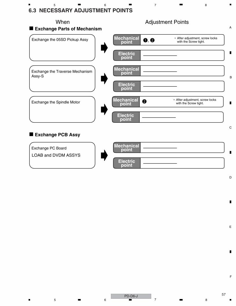
C
D
F
A
B
E
57
5 6 7 8
6.3 NECESSARY ADJUSTMENT POINTS
∗ After adjustment, screw locks with the Screw tight.~, ŸMechanical
point
Electricpoint
Mechanicalpoint
Electricpoint
Mechanicalpoint
Electricpoint
LOAB and DVDM ASSYS
Exchange Parts of Mechanism
Exchange PCB Assy
When Adjustment Points
Exchange the 05SD Pickup Assy
Exchange the Traverse Mechanism Assy-S
Exchange PC Board
∗ After adjustment, screw locks with the Screw tight.ŸMechanical
point
Electricpoint
Exchange the Spindle Motor
PD-D6-J5 6 7 8
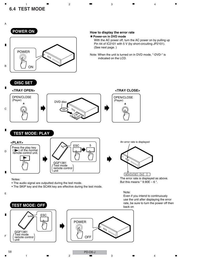
C
D
F
A
B
E
PD-D6-J58
1 2 3 4
6.4 TEST MODE
POWER ON
GGF1381Test moderemote controlunit
GGF1381Test moderemote controlunit
<TRAY OPEN> <TRAY CLOSE>
OPEN/CLOSE(Player)
OPEN/CLOSE
Press the play key ( ) of the normal remote control unit.
(Player)
TEST MODE: PLAY
TEST MODE: OFF
An error rate is displayed
ESC
<PLAY>ESC 5
DISC SET
Notes:• The audio signal are outputted during the test mode.• The SKIP key and the SCAN key are effective during the test mode.
Note: Even if you intend to continuously use the unit after displaying the error rate, be sure to turn the power off then back on
How to display the error rate Power-on in DVD mode With the AC power off, turn the AC power on by pulling up Pin 44 of IC2101 with 5 V (by short-circuiting JP2101). (See next page. ) Note: When the unit is turned on in DVD mode, "-DVD-" is indicated on the LCD.
POWER
ON
DVD disc
POWER
OFF
9 9 0 E – 6
The error rate is displayed as above.But this means " 9.90E – 6 ".
1 2 3 4
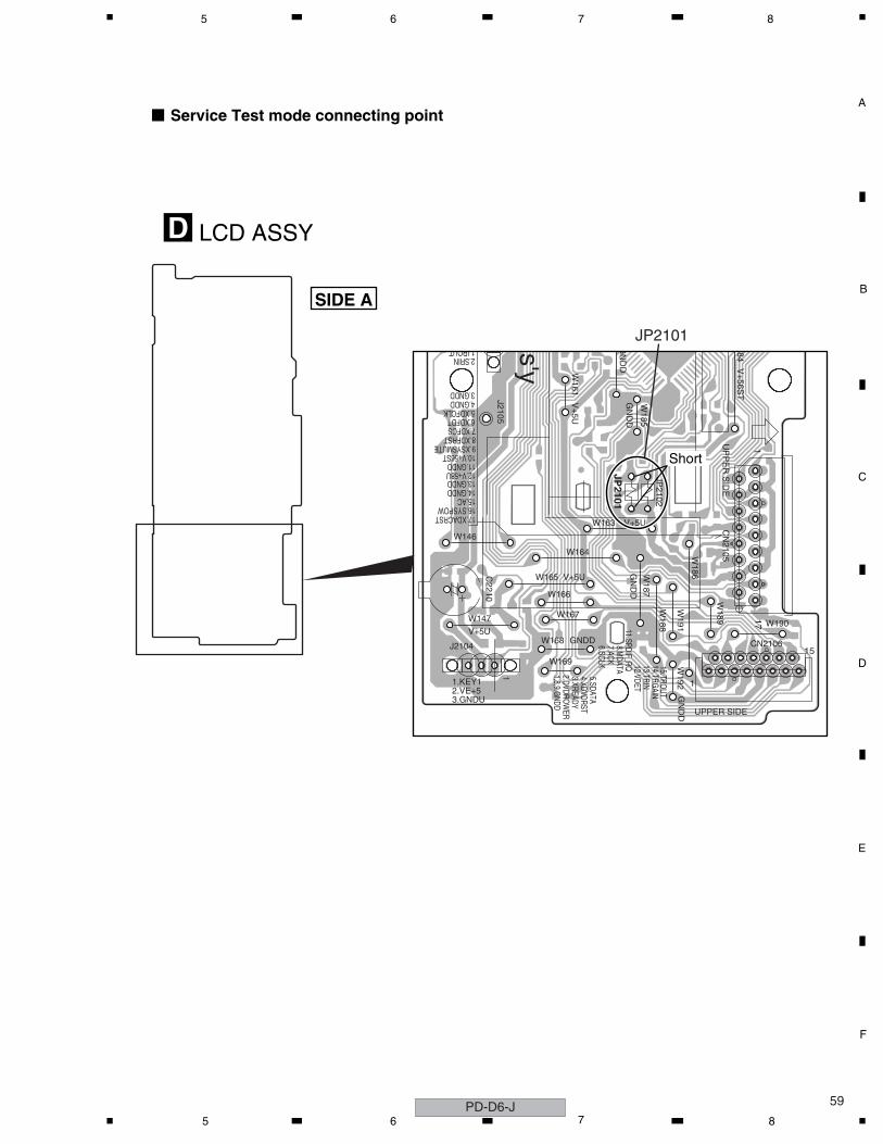
C
D
F
A
B
E
59
5 6 7 8
V+5U
V+5U
GNDD
V+5U
GN
DD
GN
DD
V+
56ST
V+
5U
GN
DD
GN
DD
UP
PE
R S
IDE
UPPER SIDE
ss'y
1IROUT2.SRIN
3.GNDD4.GNDD5.XDFCLK6.XDFDT7.XDFCS8.XDFRST9.XSYSMUTE10.V+56ST11.GNDD12.V+58U
17.XDACRST16.SYSPOW15.AC14.GNDD13.GNDD
1,8,9.GNDD
2.DVDROW
ER3.XREADY4.XDVDRST5.SDATA
6.SCLK
8.MDATA
7.ACK
11.SPDIF_RQ 12.VDET13.TRIN14.TRG
AIN15.TRO
UT
15
1
117
1
1.KEY12.VE+53.GNDU
J2105
JP2102
JP2101
W169
C2210
W146
CN2106
CN
2105
W191
W187
W186
W192
W166
W164
J2104
W167W190
W185
W168
W165
W163
84
W188
W147
W161
W189
JP2101
Short
LCD ASSY
Service Test mode connecting point
D
SIDE A
PD-D6-J5 6 7 8
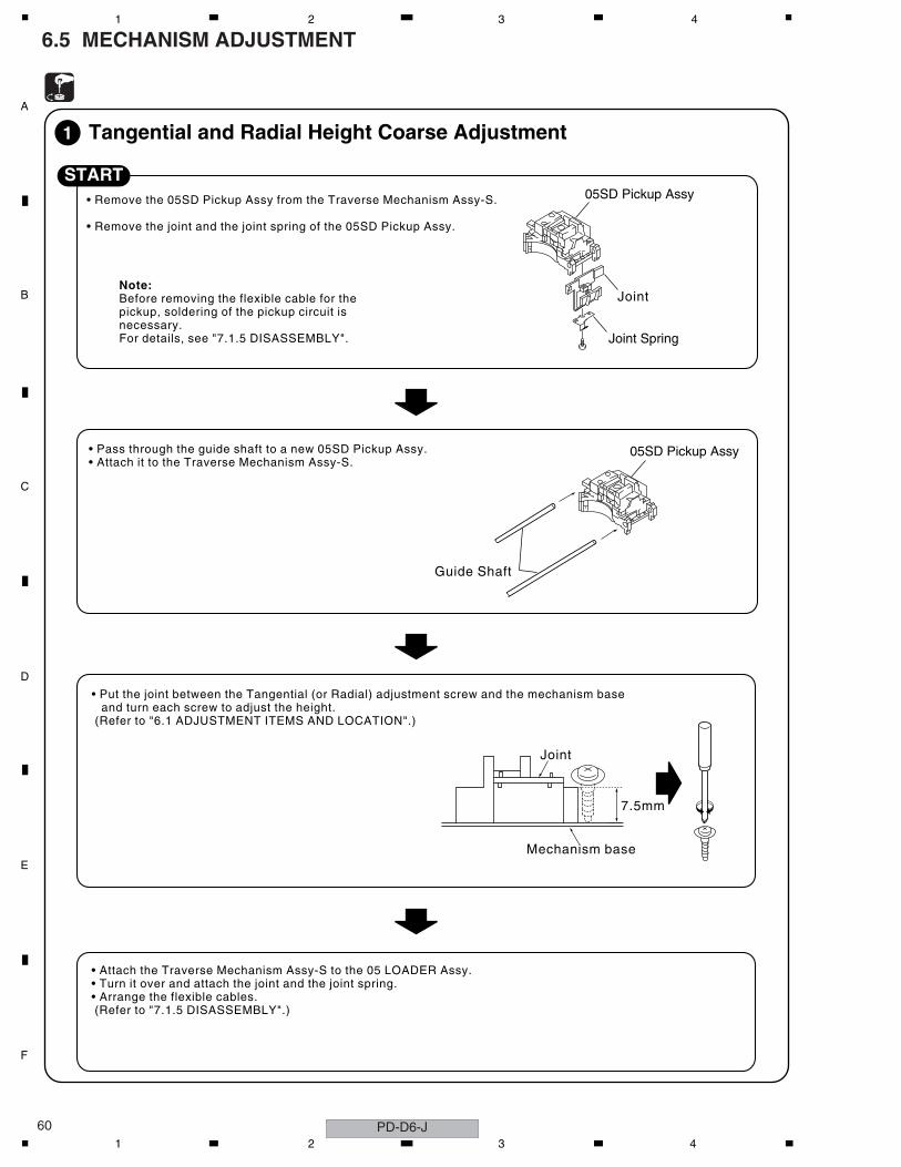
C
D
F
A
B
E
PD-D6-J60
1 2 3 4
6.5 MECHANISM ADJUSTMENT
• Remove the 05SD Pickup Assy from the Traverse Mechanism Assy-S.
• Remove the joint and the joint spring of the 05SD Pickup Assy.
• Put the joint between the Tangential (or Radial) adjustment screw and the mechanism base and turn each screw to adjust the height. (Refer to "6.1 ADJUSTMENT ITEMS AND LOCATION".)
START
Tangential and Radial Height Coarse Adjustment1
Note:Before removing the flexible cable for the pickup, soldering of the pickup circuit is necessary.For details, see "7.1.5 DISASSEMBLY".
• Pass through the guide shaft to a new 05SD Pickup Assy.• Attach it to the Traverse Mechanism Assy-S.
• Attach the Traverse Mechanism Assy-S to the 05 LOADER Assy.• Turn it over and attach the joint and the joint spring.• Arrange the flexible cables. (Refer to "7.1.5 DISASSEMBLY".)
7.5mm
Joint
Mechanism base
05SD Pickup Assy
05SD Pickup Assy
Joint
Joint Spring
Guide Shaft
1 2 3 4
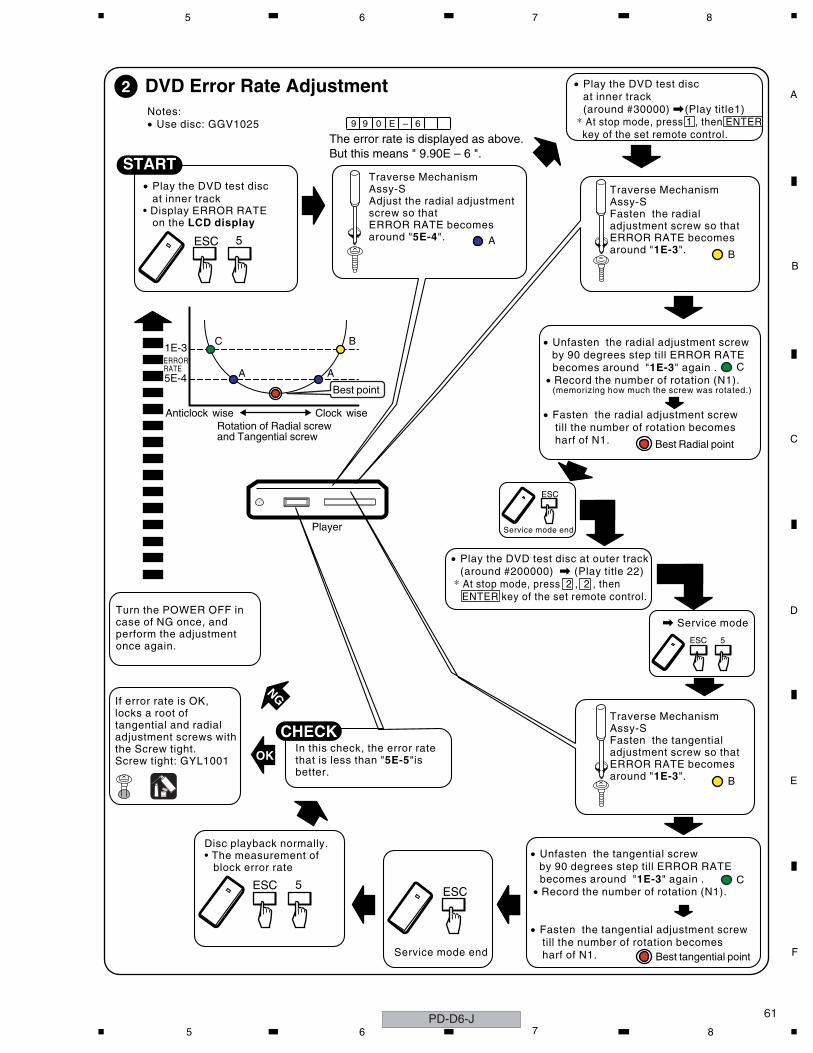
C
D
F
A
B
E
61
5 6 7 8
Player
• Play the DVD test discat inner track(around #30000) \(Play title1)
* At stop mode, press 1 , then ENTER key of the set remote control.
Traverse Mechanism Assy-SAdjust the radial adjustment screw so thatERROR RATE becomes around "5E-4".
Traverse Mechanism Assy-SFasten the radialadjustment screw so thatERROR RATE becomes around "1E-3".
START
DVD Error Rate Adjustment2
Service mode end
Disc playback normally.• The measurement of block error rate
If error rate is OK, locks a root of tangential and radial adjustment screws withthe Screw tight.Screw tight: GYL1001
Turn the POWER OFF in case of NG once, and perform the adjustment once again.
5ESC ESC
\ Service mode
Service mode end
ESC
NG
OK
• Play the DVD test discat inner track
• Display ERROR RATE on the LCD display
5ESC
Notes:• Use disc: GGV1025
• Unfasten the radial adjustment screw by 90 degrees step till ERROR RATE
becomes around "1E-3" again . • Record the number of rotation (N1).
(memorizing how much the screw was rotated.)
• Fasten the radial adjustment screw till the number of rotation becomes harf of N1.
Traverse Mechanism Assy-SFasten the tangentialadjustment screw so thatERROR RATE becomes around "1E-3".
• Unfasten the tangential screw by 90 degrees step till ERROR RATE
becomes around "1E-3" again . • Record the number of rotation (N1).
• Fasten the tangential adjustment screw till the number of rotation becomes harf of N1.
In this check, the error ratethat is less than "5E-5"isbetter.
CHECK
5ESC
AB
B
C
Best Radial point
C
Best tangential point
1E-3
5E-4
Rotation of Radial screw and Tangential screw
Anticlock wise Clock wise
Best point
A A
BC
ERROR RATE
9 9 0 E – 6
The error rate is displayed as above.But this means " 9.90E – 6 ".
• Play the DVD test disc at outer track(around #200000) \ (Play title 22)
* At stop mode, press 2 , 2 , then ENTER key of the set remote control.
PD-D6-J5 6 7 8
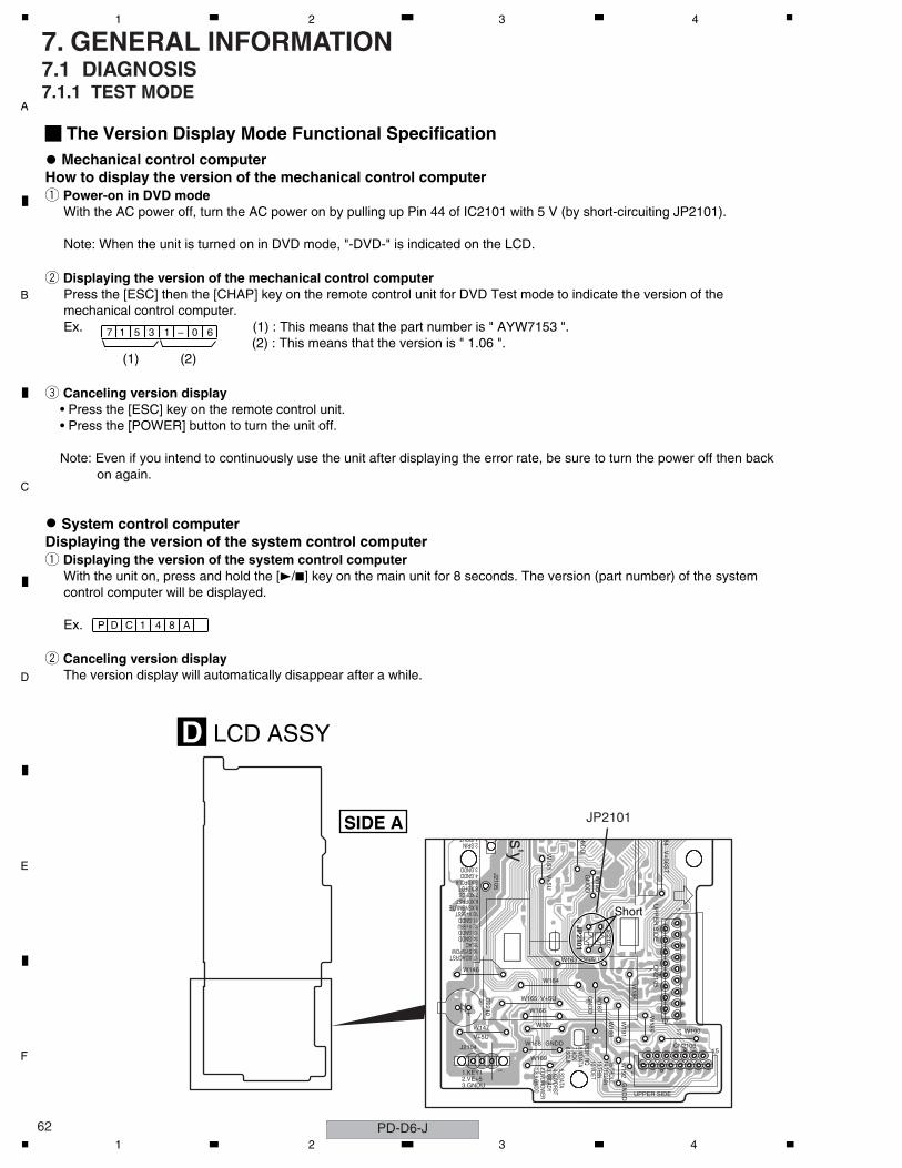
C
D
F
A
B
E
PD-D6-J62
1 2 3 4
7. GENERAL INFORMATION7.1 DIAGNOSIS7.1.1 TEST MODE
V+5U
V+5U
GNDD
V+5U
GN
DD
GN
DD
V+
56ST
V+
5U
GN
DD
GN
DD
UP
PE
R S
IDE
UPPER SIDE
ss'y
1IROUT2.SRIN
3.GNDD4.GNDD5.XDFCLK6.XDFDT7.XDFCS8.XDFRST9.XSYSMUTE10.V+56ST11.GNDD12.V+58U
17.XDACRST16.SYSPOW15.AC14.GNDD13.GNDD
1,8,9.GNDD
2.DVDROW
ER3.XREADY4.XDVDRST5.SDATA
6.SCLK
8.MDATA
7.ACK
11.SPDIF_RQ 12.VDET13.TRIN14.TRG
AIN15.TRO
UT
15
1
11
7
1
1.KEY12.VE+53.GNDU
J2105
JP2102
JP2101
W169
C2210
W146
CN2106
CN
2105
W191
W187
W186
W192
W166
W164
J2104
W167W190
W185
W168
W165
W163
84
W188
W147
W161
W189
The Version Display Mode Functional Specification Mechanical control computerHow to display the version of the mechanical control computer1 Power-on in DVD mode With the AC power off, turn the AC power on by pulling up Pin 44 of IC2101 with 5 V (by short-circuiting JP2101). Note: When the unit is turned on in DVD mode, "-DVD-" is indicated on the LCD.
2 Displaying the version of the mechanical control computer Press the [ESC] then the [CHAP] key on the remote control unit for DVD Test mode to indicate the version of the mechanical control computer. Ex. (1) : This means that the part number is " AYW7153 ". (2) : This means that the version is " 1.06 ".
3 Canceling version display • Press the [ESC] key on the remote control unit. • Press the [POWER] button to turn the unit off.
Note: Even if you intend to continuously use the unit after displaying the error rate, be sure to turn the power off then back on again.
System control computer Displaying the version of the system control computer1 Displaying the version of the system control computer With the unit on, press and hold the [3/7] key on the main unit for 8 seconds. The version (part number) of the system control computer will be displayed.
Ex.
2 Canceling version display The version display will automatically disappear after a while.
LCD ASSYD
SIDE A JP2101
Short
P D C 1 4 8 A
7 1 5 3 1 – 0 6
(1) (2)
1 2 3 4

C
D
F
A
B
E
63
5 6 7 8
7.1.2 METHOD FOR DIAGNOSING DEGRADATION OF THE LDS ON THE PICKUP ASSY
DVDM ASSYB
SIDE AFront side
R915
R914R919
R906
R904
L751
R712
Q702
C761
R714
R713C712
C133
C374
R214
R520
CN101
C215
C104
R207C213
R134
R136
C161
R154
C143
C142C141
C144
R135
C146
R132
R133
C152
R153R152
CN901
C320
C347
R918 R
913R
912R
911R
910
D
CN102
C1002
Q801
R801
R736
R751
R711
R907
R750D881
C801
D801
R737
R761
R731 C
751
Q305
C371
R325
C309
CN103
C509
Q506
IC761
R762
C345
Q881
C373
C506
R507
C752
D751
R734
C713
IC501
R502
R313
R508
R901
R903
IC711
R931
R932
R933
R934
R935R936
R937R938R939
R940
R373
R595
R594
IC101
CN
953
C505
Q
C508
Q
R505
C502
R506R504
C503
C145
R314
Q304
R315
L309 L308
R602R601
R20
C101
R131
C131
C310
R151
R310
R321
Q308
R322
R509
C102
C132
C140
C151 C153
C103
Q307
C346
R318
R905
C206
C204
C203
C221
C202
C343
C344
R59
UP SIDE
124
BOTTOM SIDE
12 G
ND
D
3.3V
5V
GNDM
6.5V
BOTTOM SIDE
BO
TT
OM
SID
E
8V
3.3V
112
543
1
4 1
UP SIDE
14
57
1
9
65
64
25
1
C
LD_CD
LD_D
VD1
345
A
D
8
54
1
E122 1
71
3.3V
LF
R326
R326
R325
R322
R321
Case when this diagnosis is required : When playback of any disc, including a test disc (DVD: GGV1025, CD: STD-905), won't play or doesn't play
How to diagnoseIn the case mentioned above, degradation of the laser diodes (LDs) mounted on the 05SD Pickup Assy is suspected.Measure the voltage between the two ends of one of the resistors mentioned below.
If the measurements show degradation of an LD, replace the 05SD Pickup Assy.
Measure the voltage between the both ends of R322 or R325 on the DVDM Assy. If the voltage is 0.4 V or higher, the 650-nm LD is degraded.
No playback of a DVD (Test Mode), No playback of a SACD :
Measure the voltage between the both ends of R321 or R326 on the DVDM Assy. If the voltage is 0.4 V or higher, the 780-nm LD is degraded.
No playback of a CD :
05SD PICKUP ASSY
CN101
PD-D6-J5 6 7 8
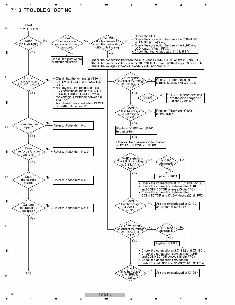
C
D
F
A
B
E
PD-D6-J64
1 2 3 4
7.1.3 TROUBLE SHOOTING
Start(Power → ON)
Doesthe LCD light?
Cancel the pure audioor dimmer function.
Refer to Addendum No. 1.
Check the connections at D1801, D1802, and CN1801.
• Check that the voltage at V2201 1is 4.4 V and that that at V2201 2is 5 V.
• Are any data transmitted on the LCD communication line (LCCDT,LCDCK, LCDCS, LCDRS) when the voltage is switched between 0and 5 V?
• Are H and L switched when BLOFFor DIMMER functions?
• Check the FU1.• Check the connection between the PRIMARY
and AJKB (4 pin) Assys.• Check the connection between the AJKB and
LCD Assys (17-pin FFC).• Check that the voltage at J11 3 is 5.6 V.
• Check the connections at D1851 and CN1801.• Check the connection between the AJKB
and CONNECTOR Assys (15-pin FFC).• Check the connection between the
CONNECTOR and DVDM Assys (29-pin FFC).
• Is D1809 short-circuited?• Are the pins bridged at
IC1301 or IC1401?
Checkthat the voltageat C1805(+) is
+12 V.
Yes
Yes
No
[V+5A]No
No
Doesthe pure audio
or dimmer functionoperate?
Are the indications on
the LCD correct?
Yes
NoDoes the trayopen?
Refer to Addendum No. 2.
Yes
NoDoesthe focus function
operate?
Refer to Addendum No. 3.
Yes
NoDoesthe spindle
rotate?
Refer to Addendum No. 4.
Yes
NoCan anyoperation be
stopped?
Yes
No
• Check the connection between the AJKB and CONNECTOR Assys (15-pin FFC).• Check the connection between the CONNECTOR and DVDM Assys (29-pin FFC).• Check the voltages at V+12A, V+5A, V+9D, and V+6R5V.
Yes
Yes
Yes
No
No
Replace D1805 and Q1801,in that order.
Replace D1807 and Q1803,in that order.
Yes
Check if the pins are short-circuitedat IC1101, IC1201, or IC1102.
No
Checkthat the voltage
at V+3D is +3.3 V.
Are the pins bridged at IC1301or IC1401 or IC1501?
No
Is IC1851damaged?
Yes
Replace IC1851.
No
The LCDdisplay goes dark,and the pure audioLED starts flashing.
[V+12V system]Check that the voltage
at C1803(+) is +17 V.
Yes
No[V+9D system]Check that the voltage
at C1852(+) is +8.3 V.
• Check the connections at D1852 and CN1801.• Check the connection between the AJKB
and CONNECTOR Assys (15-pin FFC).• Check the connection between the
CONNECTOR and DVDM Assys (29-pin FFC).
Checkthat the voltageat V+6R5V is
+6.5 V.
Are the pins bridged at IC101?No
Is IC1852damaged?
Yes
Replace IC1852.
No
Yes
No[V+6R5V system]Check that the voltage
at C1854(+) is +11 V.
A
1 2 3 4
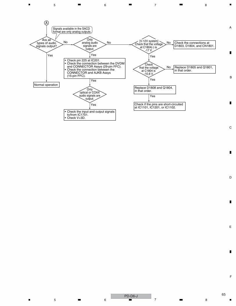
C
D
F
A
B
E
65
5 6 7 8
Normal operation
Check the connections at D1803, D1804, and CN1801.
Checkthat the voltage
at C1804 is -10.8 V.
Yes
NoOnly
analog audiosignals are
output.
Signals available in the SACDformat are only analog outputs.
Are alltypes of audiosignals output?
Yes
Onlyoptical or COAXaudio signals are
output.
Yes
Yes
No
• Check pin 225 at IC201.• Check the connection between the DVDM
and CONNECTOR Assys (29-pin FFC).• Check the connection between the
CONNECTOR and AJKB Assys(15-pin FFC).
• Check the input and output signalsto/from IC1701.
• Check V+3D.
Yes
Yes
No
Replace D1805 and Q1801,in that order.
Replace D1808 and Q1804,in that order.
Yes
Check if the pins are short-circuitedat IC1101, IC1201, or IC1102.
No
[V-12V system]Check that the voltage
at C1804(-) is -17 V.
A
PD-D6-J5 6 7 8
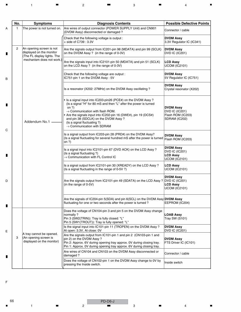
C
D
F
A
B
E
PD-D6-J66
1 2 3 4
No. Symptoms Diagnosis Contents Possible Defective Points1 The power is not turned on. Are wires of output connector (POWER SUPPLY Unit) and CN901
(DVDM Assy) disconnected or damaged ?Connector / cable
Check that the following voltage is output :+ side of C739 : 3.3V
DVDM Assy3.3V Regulator IC (IC341)
2 An opening screen is not displayed on the monitor(The FL display lights. The mechanism does not work.)
Are the signals output from IC201-pin 98 (MDATA) and pin 99 (SCLK) on the DVDM Assy ? (in the range of 0-3V)
DVDM AssyDVD IC (IC201)
Are the signals input into IC2101-pin 50 (MDATA) and pin 51 (SCLK) on the LCD Assy ? (in the range of 0-3V)
LCD AssyUCOM (IC2101)
Check that the following voltage are output :IC751-pin 1 on the DVDM Assy : 5V
DVDM Assy5V Regulator IC (IC751)
Is a resonator (X202: 27MHz) on the DVDM Assy oscillating ?DVDM AssyCrystal resonator (X202)
• Is a signal input into IC203-pin26 (PCE#) on the DVDM Assy ? (Is a signal "H" for 80 mS and then "L" after the power is turned on ?)→ Communication with flash ROM.
• Are the signals input into IC202-pin 16 (DWE#), pin 19 (DCS#) and pin 38 (SDCLK) on the DVDM Assy ?(Is a signal fluctuating ?)→ Communication with SDRAM
DVDM AssyDVD IC (IC201)Flash ROM (IC203)SDRAM (IC202)
Is a signal output from IC203-pin 28 (PRD#) on the DVDM Assy?(Is a signal fluctuating for several hundred mS after the power is turned on ?)
DVDM AssyFlash ROM (IC203)
Is a signal input into IC2101-pin 67 (DVD ACK) on the LCD Assy ? (Is a signal fluctuating ?)→ Communication with FL Control IC
DVDM AssyDVD IC (IC201)LCD AssyUCOM (IC2101)
Is a signal output from IC2101-pin 30 (XREADY) on the LCD Assy ? (Is a signal fluctuating in the range of 0-5V ?)
LCD AssyUCOM (IC2101)
Are the signals output from IC2101-pin 49 (SDATA) on the LCD Assy ? (in the range of 0-5V)
DVDM AssyDVD IC (IC201)LCD AssyUCOM (IC2101)
Are the signals of IC204-pin 5(SDA) and pin 6(SCL) on the DVDM Assy fluctuating for one or two seconds after the power is turned ?
DVDM AssyEEPROM (IC204)
Addendum No.1
3A tray cannot be opened.(An opening screen is displayed on the monitor)
LOAB AssyTray SW (S101)
Is the signal input into IC101-pin 11 (TROPEN) on the DVDM Assy ?At open: 3.3V, At close: 0V
DVDM AssyDVD IC (IC201)
Are the signals output from IC101-pin 1 and pin 2 (CN103-pin 1 and pin 2) on the DVDM Assy ?Pin 2: Approx. 6V during opening tray approx. 0V during closing tray.Pin 1: Approx. 0V during opening tray approx. 6V during closing tray.
DVDM AssyFTS Driver IC (IC101)
Are wires of CN104 and CN103 on the DVDM Assy disconnected or damaged ?
Connector / cable
Does the voltage of CN102-pin 1 on the DVDM Assy change to 0V by pressing the Inside switch.
Inside switch
Does the voltage of CN104-pin 3 and pin 5 on the DVDM Assy change normally ?Pin 3 (SW2(TRIN)): Tray is fully closed: "L"Pin 5 (SW1(TROUT)): Tray is fully opened: "L"
1 2 3 4
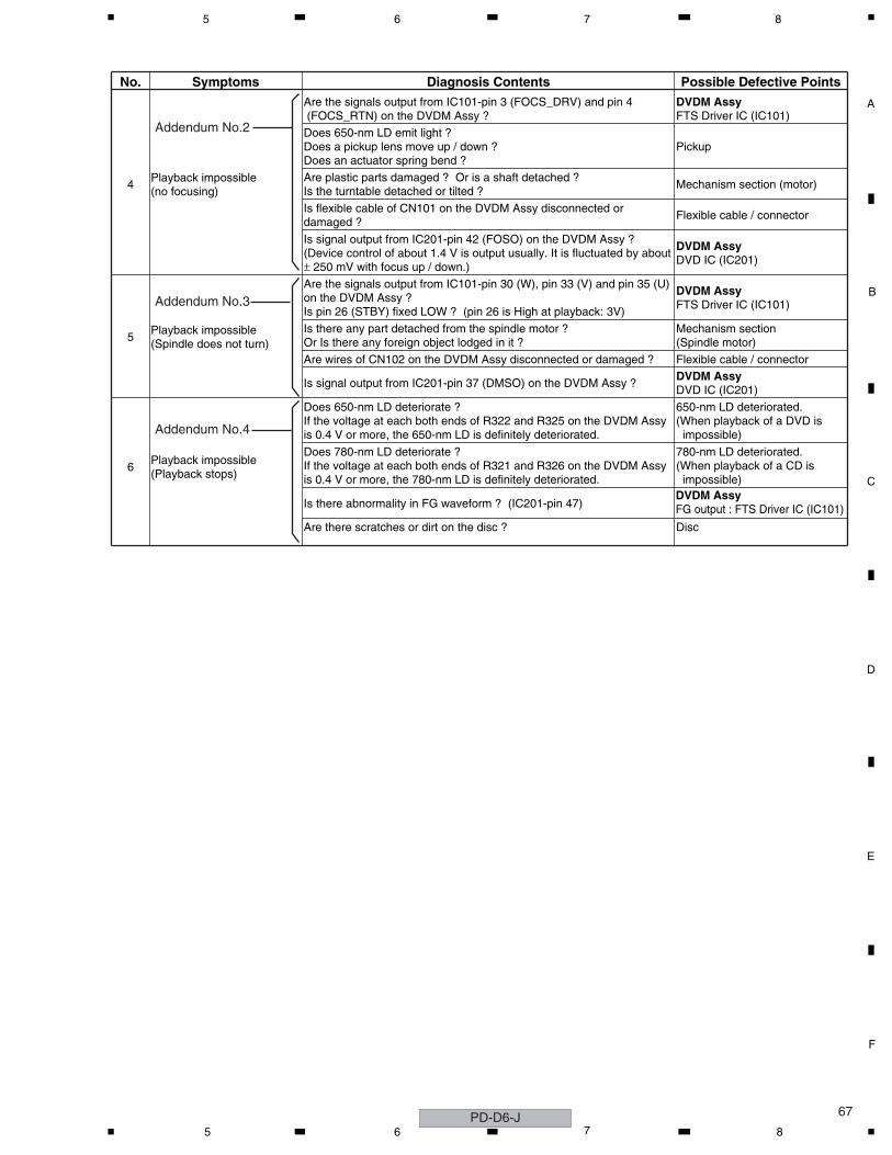
C
D
F
A
B
E
67
5 6 7 8
No. Symptoms Diagnosis Contents Possible Defective Points
4Playback impossible(no focusing)
Are the signals output from IC101-pin 3 (FOCS_DRV) and pin 4 (FOCS_RTN) on the DVDM Assy ?
DVDM AssyFTS Driver IC (IC101)
Does 650-nm LD emit light ?Does a pickup lens move up / down ?Does an actuator spring bend ?
Pickup
Are plastic parts damaged ? Or is a shaft detached ?Is the turntable detached or tilted ?
Mechanism section (motor)
Is flexible cable of CN101 on the DVDM Assy disconnected or damaged ?
Flexible cable / connector
Is signal output from IC201-pin 42 (FOSO) on the DVDM Assy ?(Device control of about 1.4 V is output usually. It is fluctuated by about ± 250 mV with focus up / down.)
DVDM AssyDVD IC (IC201)
5Playback impossible(Spindle does not turn)
Are the signals output from IC101-pin 30 (W), pin 33 (V) and pin 35 (U) on the DVDM Assy ?Is pin 26 (STBY) fixed LOW ? (pin 26 is High at playback: 3V)
DVDM AssyFTS Driver IC (IC101)
Is there any part detached from the spindle motor ?Or Is there any foreign object lodged in it ?
Mechanism section(Spindle motor)
Are wires of CN102 on the DVDM Assy disconnected or damaged ? Flexible cable / connector
Is signal output from IC201-pin 37 (DMSO) on the DVDM Assy ?DVDM AssyDVD IC (IC201)
6Playback impossible(Playback stops)
Does 650-nm LD deteriorate ?If the voltage at each both ends of R322 and R325 on the DVDM Assy is 0.4 V or more, the 650-nm LD is definitely deteriorated.
650-nm LD deteriorated.(When playback of a DVD is impossible)
Does 780-nm LD deteriorate ?If the voltage at each both ends of R321 and R326 on the DVDM Assy is 0.4 V or more, the 780-nm LD is definitely deteriorated.
780-nm LD deteriorated.(When playback of a CD is impossible)
Is there abnormality in FG waveform ? (IC201-pin 47)DVDM AssyFG output : FTS Driver IC (IC101)
Are there scratches or dirt on the disc ? Disc
Addendum No.2
Addendum No.4
Addendum No.3
PD-D6-J5 6 7 8
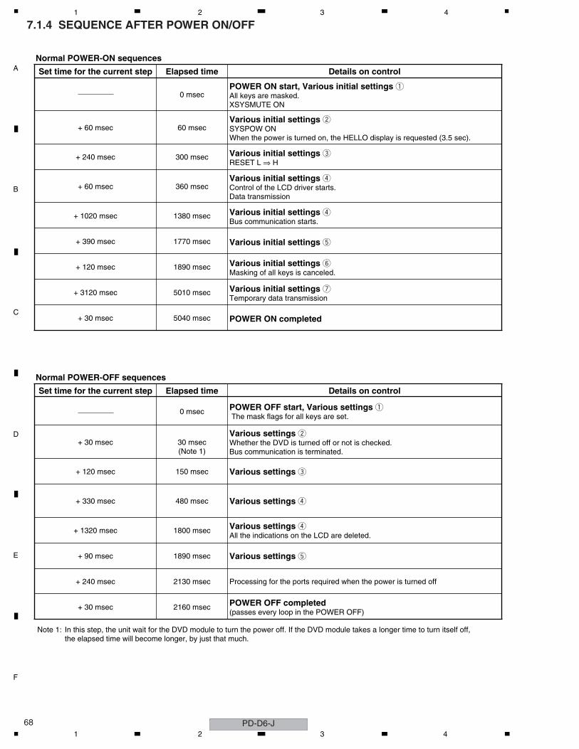
C
D
F
A
B
E
PD-D6-J68
1 2 3 4
7.1.4 SEQUENCE AFTER POWER ON/OFF
Set time for the current step Elapsed time Details on control
0 msecPOWER ON start, Various initial settings 1All keys are masked.XSYSMUTE ON
+ 60 msec 60 msecVarious initial settings 2SYSPOW ONWhen the power is turned on, the HELLO display is requested (3.5 sec).
+ 240 msec 300 msec Various initial settings 3RESET L ⇒ H
+ 60 msec 360 msecVarious initial settings 4Control of the LCD driver starts.Data transmission
+ 1020 msec 1380 msec Various initial settings 4Bus communication starts.
+ 390 msec 1770 msec Various initial settings 5
+ 120 msec 1890 msec Various initial settings 6Masking of all keys is canceled.
+ 3120 msec 5010 msec Various initial settings 7Temporary data transmission
+ 30 msec 5040 msec POWER ON completed
Normal POWER-ON sequences
Normal POWER-OFF sequences
Set time for the current step Elapsed time Details on control
0 msec POWER OFF start, Various settings 1 The mask flags for all keys are set.
+ 30 msec 30 msec(Note 1)
Various settings 2Whether the DVD is turned off or not is checked.Bus communication is terminated.
+ 120 msec 150 msec Various settings 3
+ 330 msec 480 msec Various settings 4
+ 1320 msec 1800 msec Various settings 4All the indications on the LCD are deleted.
+ 90 msec 1890 msec Various settings 5
+ 240 msec 2130 msec Processing for the ports required when the power is turned off
+ 30 msec 2160 msec POWER OFF completed(passes every loop in the POWER OFF)
Note 1: In this step, the unit wait for the DVD module to turn the power off. If the DVD module takes a longer time to turn itself off, the elapsed time will become longer, by just that much.
1 2 3 4
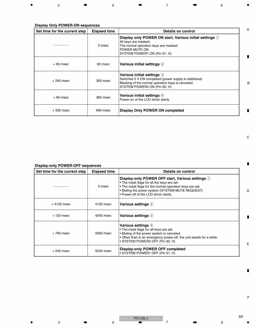
C
D
F
A
B
E
69
5 6 7 8
Display Only POWER-ON sequences
Display-only POWER-OFF sequences
Set time for the current step Elapsed time Details on control
0 msec
Display only POWER ON start, Various initial settings 1All keys are masked.The normal operation keys are masked.POWER MUTE ONSYSTEM POWER1 ON (Pin 91: H)
+ 60 msec 60 msec Various initial settings 2
+ 240 msec 300 msec
Various initial settings 3Switched 5 V ON completed (power supply is stabilized)Masking of the normal operation keys is canceled.SYSTEM POWER2 ON (Pin 92: H)
+ 60 msec 360 msec Various initial settings 4Power-on of the LCD driver starts.
+ 330 msec 690 msec Display Only POWER ON completed
Set time for the current step Elapsed time Details on control
0 msec
Display-only POWER OFF start, Various settings 1• The mask flags for all the keys are set.• The mask flags for the normal operation keys are set.• Muting the power system (SYSTEM MUTE REQUEST)• Power-off of the LCD driver starts.
+ 4120 msec 4120 msec Various settings 2
+ 120 msec 4240 msec Various settings 3
+ 760 msec 5000 msec
Various settings 4• The mask flags for all keys are set.• Muting of the power system is canceled.• Other than in an emergency power-off, the unit awaits for a while.• SYSTEM POWER2 OFF (Pin 92: H)
+ 240 msec 5240 msec Display-only POWER OFF completed• SYSTEM POWER1 OFF (Pin 91: H)
PD-D6-J5 6 7 8
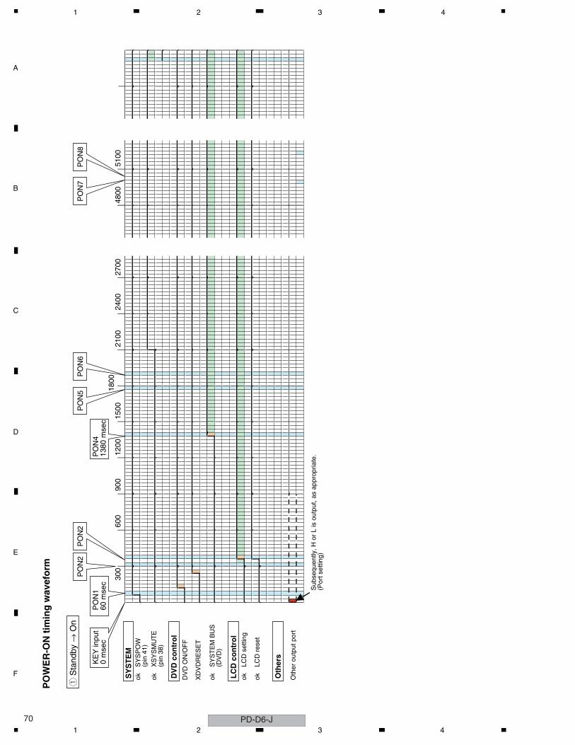
C
D
F
A
B
E
PD-D6-J70
1 2 3 4
1 S
tand
by →
On
KE
Y in
put
0 m
sec
okS
YS
PO
W(p
in 4
1)ok
XS
YS
MU
TE
(pin
38)
DV
D O
N/O
FF
XD
VD
RE
SE
T
okS
YS
TE
M B
US
(DV
D)
okLC
D s
ettin
g
okLC
D r
eset
Oth
er o
utpu
t por
t
Sub
sequ
ently
, H o
r L
is o
utpu
t, as
app
ropr
iate
.(P
ort s
ettin
g)
SY
ST
EM
DV
D c
on
tro
l
LC
D c
on
tro
l
Oth
ers
PO
N1
60 m
sec
PO
N4
1380
mse
c
PO
N2
PO
N5
PO
N6
PO
N7
PO
N8
PO
N2
300
600
900
1200
1500
1800
2100
2400
2700
4800
5100
PO
WE
R-O
N t
imin
g w
avef
orm
1 2 3 4
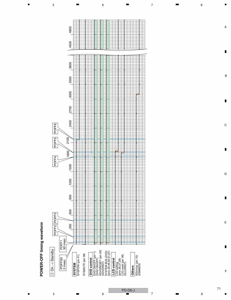
C
D
F
A
B
E
71
5 6 7 8
2 O
n →
Sta
ndby
PO
FF
G0
0 m
sec
SY
SP
OW
(pi
n 41
)
SY
SM
UT
E (
pin
38)
DV
D O
N/O
FF
(pi
n 1)
(DV
D O
N/O
FF
)X
DV
DR
ES
ET
(pi
n 93
)(X
DV
DR
ST
)S
YS
TE
M B
US
(D
VD
)(p
ins
30,4
9,50
,51,
67)
LCD
set
ting
(pin
s 26
,27,
28)
LCD
res
et (
pin
36)
(XLC
DR
ST
)
XD
imm
er (
pin
70)
(DIM
ME
R)
SY
ST
EM
DV
D c
on
tro
l
LC
D c
on
tro
l
Oth
ers
PO
FF
130
mse
c
PO
FF
2P
OF
F3
PO
FF
4P
OF
F5
PO
FF
6
300
600
900
1200
1500
1800
2100
2400
2700
3000
3300
3600
4500
4800
PO
WE
R-O
FF
tim
ing
wav
efo
rm
PD-D6-J5 6 7 8
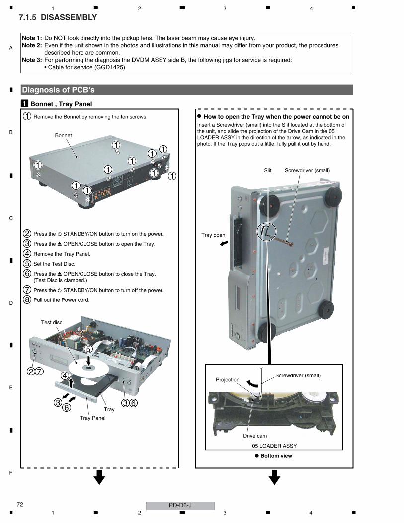
C
D
F
A
B
E
PD-D6-J72
1 2 3 4
7.1.5 DISASSEMBLY
1 Remove the Bonnet by removing the ten screws.
2 Press the STANDBY/ON button to turn on the power.
3 Press the 0 OPEN/CLOSE button to open the Tray.
4 Remove the Tray Panel.
5 Set the Test Disc.
6 Press the 0 OPEN/CLOSE button to close the Tray.(Test Disc is clamped.)
7 Press the STANDBY/ON button to turn off the power.
8 Pull out the Power cord.
Bonnet , Tray Panel1
36
5
4
Tray Panel
Screwdriver (small)
Screwdriver (small)
05 LOADER ASSY
Tray open
Slit
Test disc
Tray
How to open the Tray when the power cannot be onInsert a Screwdriver (small) into the Slit located at the bottom of the unit, and slide the projection of the Drive Cam in the 05 LOADER ASSY in the direction of the arrow, as indicated in the photo. If the Tray pops out a little, fully pull it out by hand.
Diagnosis of PCB's
Note 1: Do NOT look directly into the pickup lens. The laser beam may cause eye injury.Note 2: Even if the unit shown in the photos and illustrations in this manual may differ from your product, the procedures
described here are common.Note 3: For performing the diagnosis the DVDM ASSY side B, the following jigs for service is required:
• Cable for service (GGD1425)
72
Drive cam
Projection
Bottom view
1
11
11
11
11
1
63
Bonnet
1 2 3 4
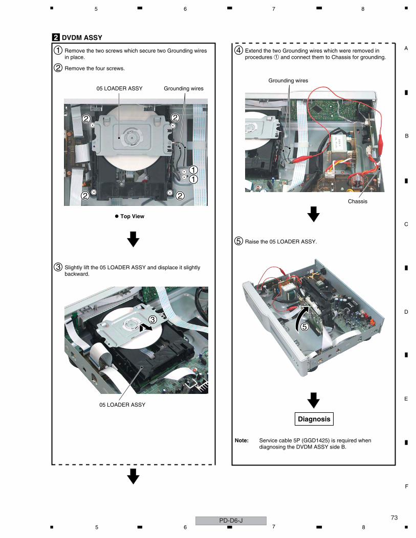
C
D
F
A
B
E
73
5 6 7 8
3
22
2 2
11
Grounding wires05 LOADER ASSY
05 LOADER ASSY
Chassis
5
Grounding wires
DVDM ASSY2
1 Remove the two screws which secure two Grounding wires in place.
3 Slightly lift the 05 LOADER ASSY and displace it slightly backward.
4 Extend the two Grounding wires which were removed in procedures 1 and connect them to Chassis for grounding.
5 Raise the 05 LOADER ASSY.
Top View
Remove the four screws.2
Diagnosis
Note: Service cable 5P (GGD1425) is required when diagnosing the DVDM ASSY side B.
PD-D6-J5 6 7 8
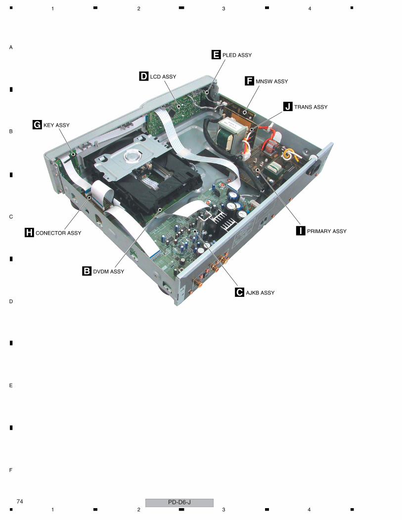
C
D
F
A
B
E
PD-D6-J74
1 2 3 4
KEY ASSYG
LCD ASSYD
PLED ASSYE
MNSW ASSYF
AJKB ASSYC
PRIMARY ASSYI
TRANS ASSYJ
CONECTOR ASSYH
DVDM ASSYB
1 2 3 4
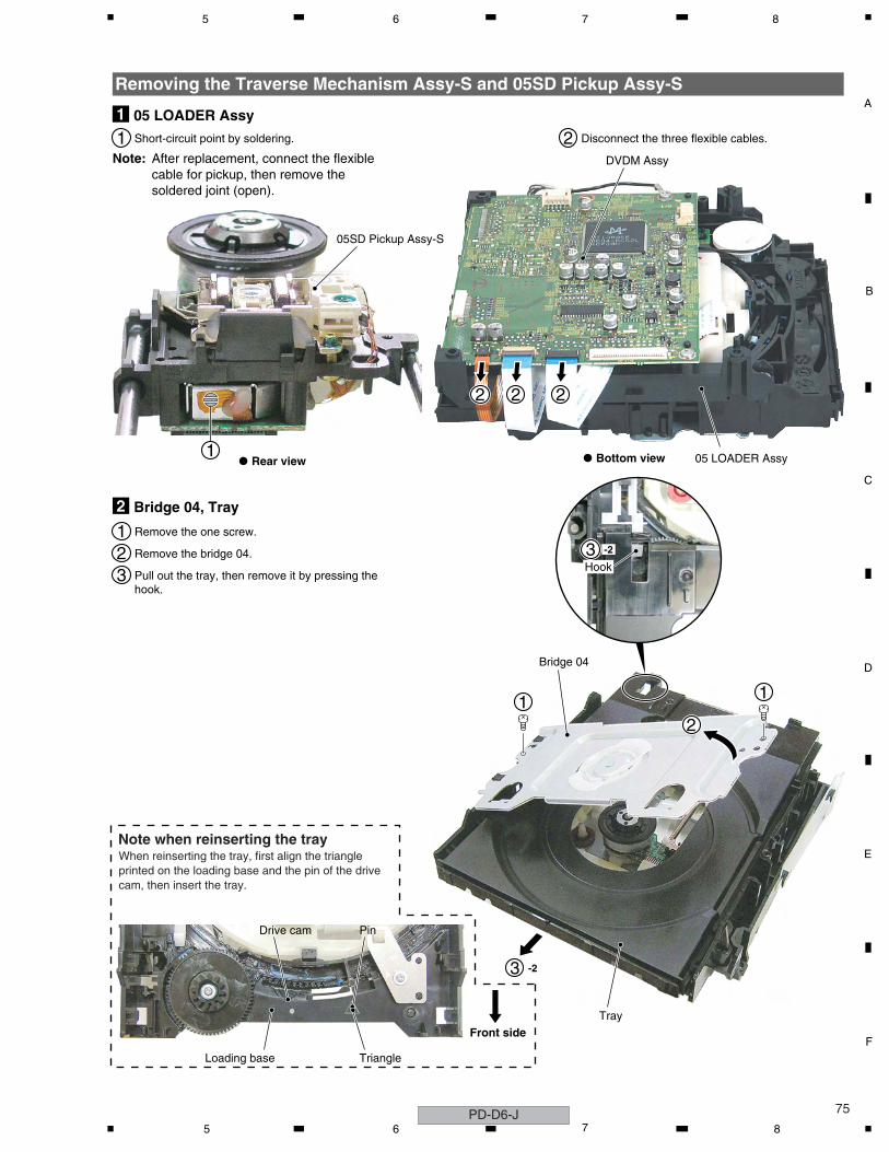
C
D
F
A
B
E
75
5 6 7 8
Removing the Traverse Mechanism Assy-S and 05SD Pickup Assy-S
105 LOADER Assy1Short-circuit point by soldering. 2 Disconnect the three flexible cables.
Note: After replacement, connect the flexible cable for pickup, then remove the soldered joint (open).
1
222
Rear view Bottom view
DVDM Assy
05 LOADER Assy
05SD Pickup Assy-S
1 Remove the one screw.
2 Remove the bridge 04.
3 Pull out the tray, then remove it by pressing the hook.
1
2
3
Bridge 04
Front side
Hook
Tray
Loading base Triangle
PinDrive cam
-2
3 -2
Note when reinserting the trayWhen reinserting the tray, first align the triangle printed on the loading base and the pin of the drive cam, then insert the tray.
Bridge 04, Tray2
1
PD-D6-J5 6 7 8
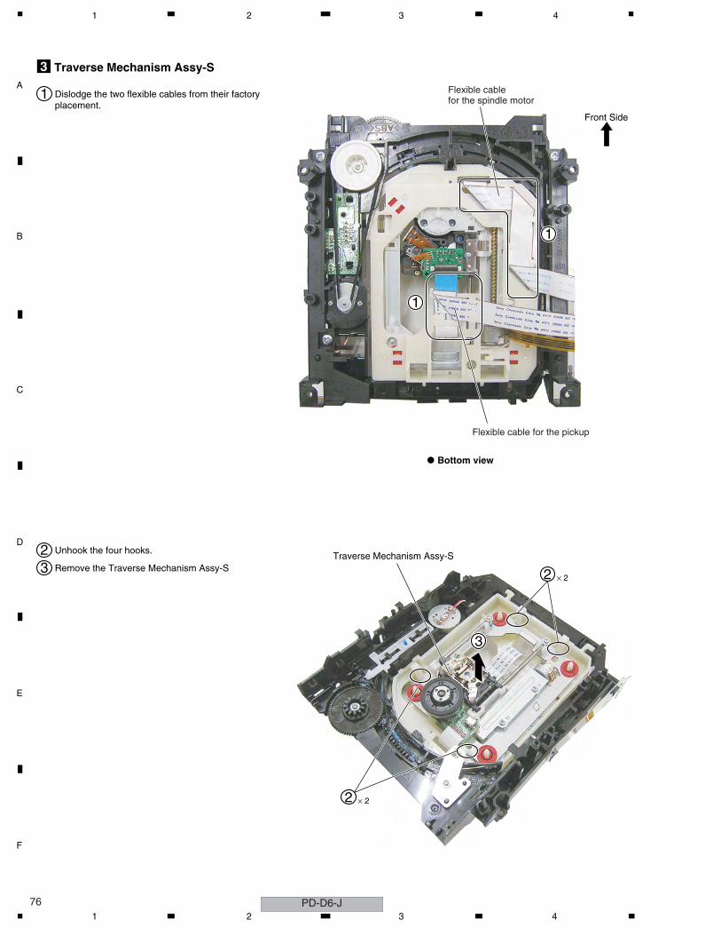
C
D
F
A
B
E
PD-D6-J76
1 2 3 4
1
Traverse Mechanism Assy-S3
Dislodge the two flexible cables from their factory placement.
2 Unhook the four hooks.
3 Remove the Traverse Mechanism Assy-S× 22
× 22
3
Traverse Mechanism Assy-S
1
1
Front Side
Flexible cable for the spindle motor
Flexible cable for the pickup
Bottom view
1 2 3 4
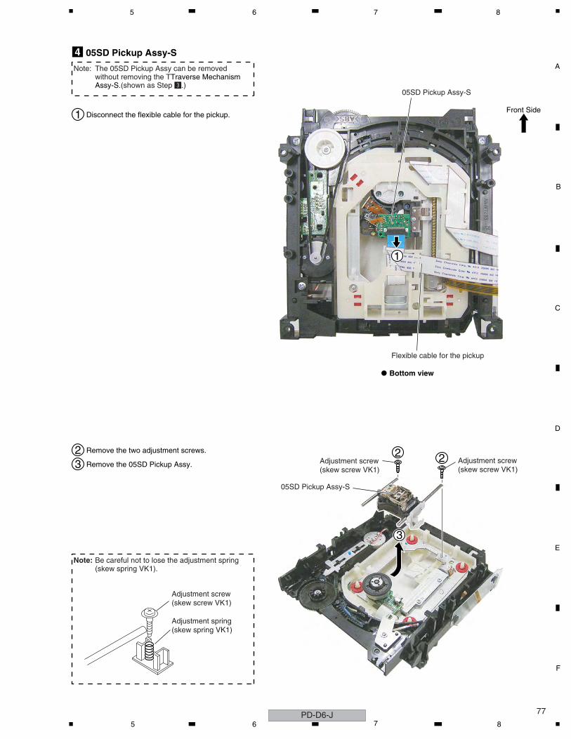
C
D
F
A
B
E
77
5 6 7 8
3
22Adjustment screw(skew screw VK1)
Adjustment screw(skew screw VK1)
Adjustment screw(skew screw VK1)
Adjustment spring(skew spring VK1)
05SD Pickup Assy-S4
Note: The 05SD Pickup Assy can be removed without removing the TTraverse MechanismAssy-S.(shown as Step π.)
Note: Be careful not to lose the adjustment spring (skew spring VK1).
Flexible cable for the pickup
05SD Pickup Assy-S
1
Front Side1 Disconnect the flexible cable for the pickup.
2 Remove the two adjustment screws.
3 Remove the 05SD Pickup Assy.
Bottom view
05SD Pickup Assy-S
PD-D6-J5 6 7 8
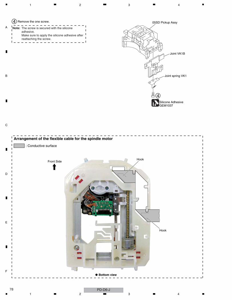
C
D
F
A
B
E
PD-D6-J78
1 2 3 4
Note: The screw is secured with the silicone adhesive. Make sure to apply the silicone adhesive afterreattaching the screw.
4 Remove the one screw.
4Silicone AdhesiveGEM1037
05SD Pickup Assy
Joint VK1B
Joint spring VK1
: Conductive surface
Arrangement of the flexible cable for the spindle motor
Front Side
Hook
Hook
Bottom view
1 2 3 4
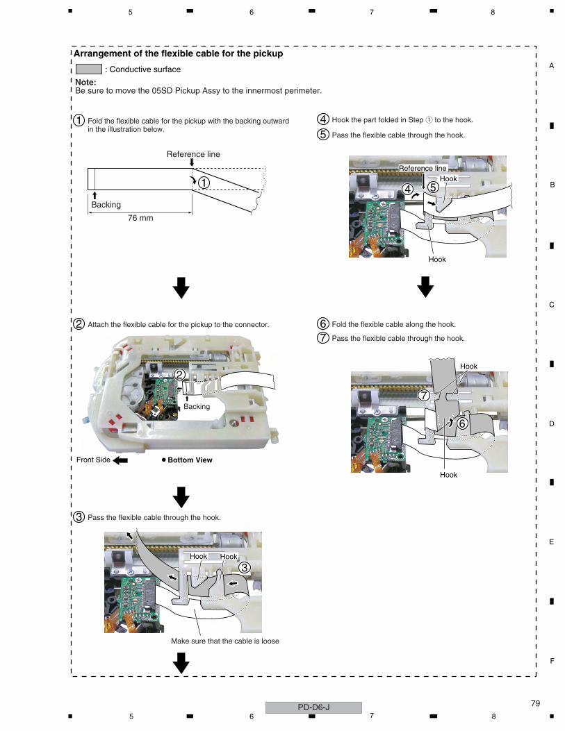
C
D
F
A
B
E
79
5 6 7 8
Front Side
Note: Be sure to move the 05SD Pickup Assy to the innermost perimeter.
: Conductive surface
Arrangement of the flexible cable for the pickup
2
3
7
2 Attach the flexible cable for the pickup to the connector. 6 Fold the flexible cable along the hook.
7 Pass the flexible cable through the hook.
3 Pass the flexible cable through the hook.
Bottom View
Make sure that the cable is loose
Backing
Backing
Reference line
Hook
Hook
4 5
5 Pass the flexible cable through the hook.
4 Hook the part folded in Step 1 to the hook.
HookReference line
6
Hook
1 Fold the flexible cable for the pickup with the backing outwardin the illustration below.
76 mm
1
HookHook
PD-D6-J5 6 7 8
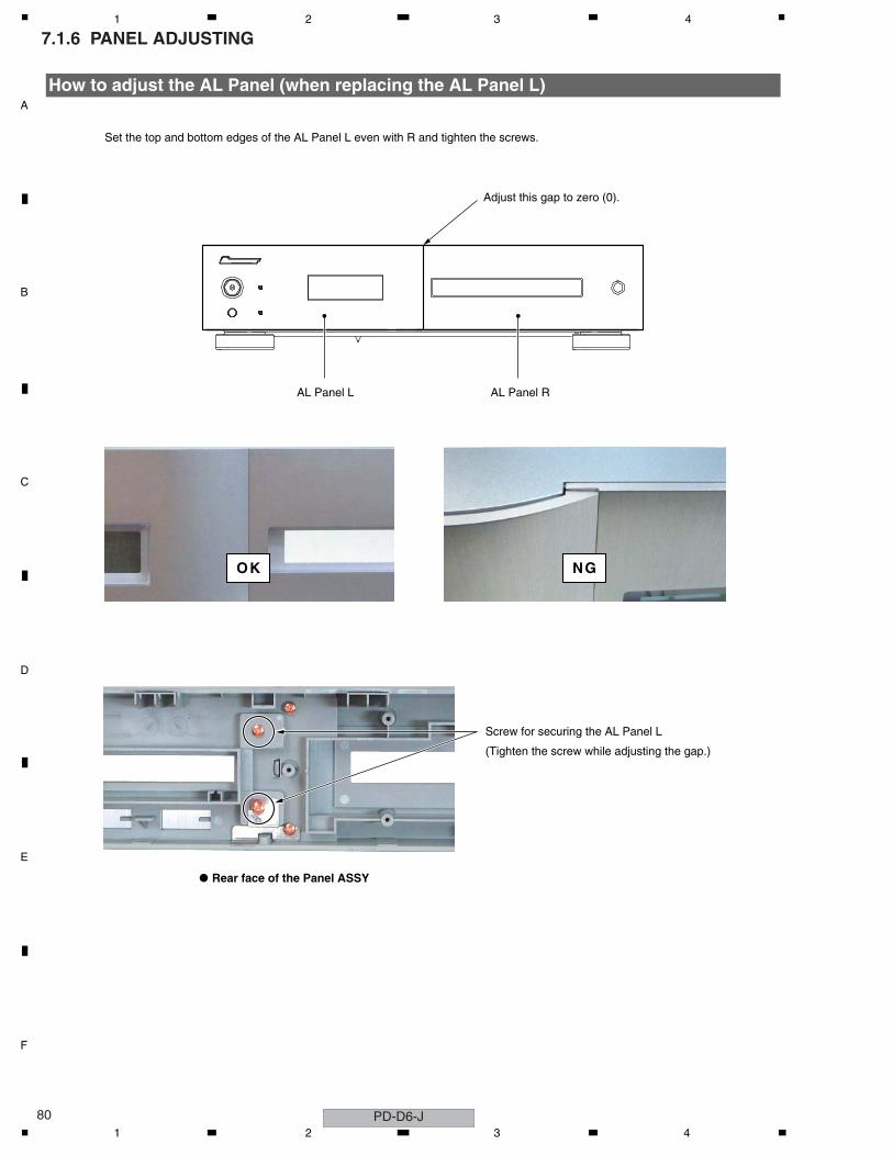
C
D
F
A
B
E
PD-D6-J80
1 2 3 4
7.1.6 PANEL ADJUSTING
How to adjust the AL Panel (when replacing the AL Panel L)
AL Panel L AL Panel R
Adjust this gap to zero (0).
Set the top and bottom edges of the AL Panel L even with R and tighten the screws.
Screw for securing the AL Panel L
(Tighten the screw while adjusting the gap.)
OK NG
Rear face of the Panel ASSY
1 2 3 4
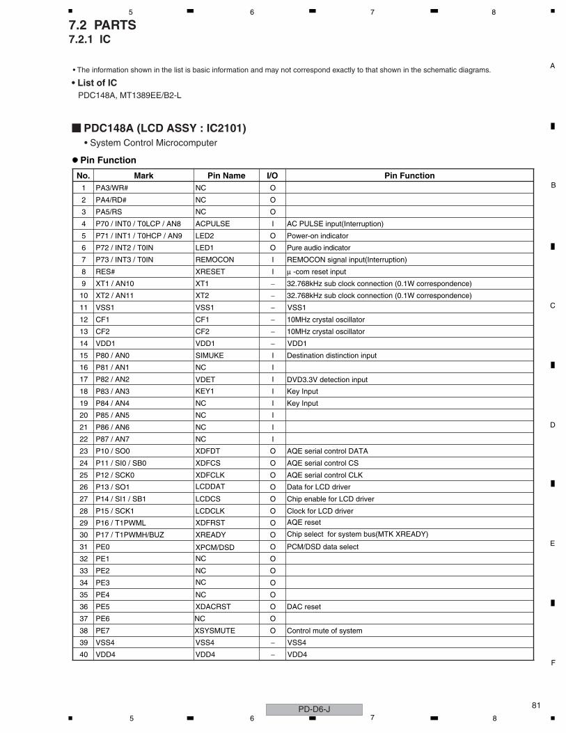
C
D
F
A
B
E
81
5 6 7 8
7.2 PARTS7.2.1 IC
PDC148A (LCD ASSY : IC2101)• System Control Microcomputer
Pin Function
No. Mark Pin Name I/O Pin Function1 PA3/WR# O
2 PA4/RD# O
3 PA5/RS O
4 P70 / INT0 / T0LCP / AN8 ACPULSE
NC
NC
NC
I AC PULSE input(Interruption)
5 P71 / INT1 / T0HCP / AN9 LED2 O Power-on indicator
6 P72 / INT2 / T0IN LED1 O Pure audio indicator
7 P73 / INT3 / T0IN REMOCON I REMOCON signal input(Interruption)
8 RES# XRESET I µ -com reset input
9 XT1 / AN10 XT1 − 32.768kHz sub clock connection (0.1W correspondence)
10 XT2 / AN11 XT2 − 32.768kHz sub clock connection (0.1W correspondence)
11 VSS1 VSS1 − VSS1
12 CF1 CF1 − 10MHz crystal oscillator
13 CF2 CF2 − 10MHz crystal oscillator
14 VDD1 VDD1 − VDD1
15 P80 / AN0 SIMUKE I Destination distinction input
16 P81 / AN1 NC I
17 P82 / AN2 I
18 P83 / AN3 I
19 P84 / AN4 NC I Key Input
VDET DVD3.3V detection input
20 P85 / AN5 I
21 P86 / AN6 NC
NC
KEY1
I
Key Input
22 P87 / AN7 NC I
23 P10 / SO0 XDFDT O AQE serial control DATA
24 P11 / SI0 / SB0 XDFCS O AQE serial control CS
25 P12 / SCK0 XDFCLK O AQE serial control CLK
26 P13 / SO1 O
27 P14 / SI1 / SB1 LCDCS
LCDDAT
O Chip enable for LCD driver
Data for LCD driver
28 P15 / SCK1 LCDCLK O Clock for LCD driver
29 P16 / T1PWML O
30 P17 / T1PWMH/BUZ O
31 PE0 O
32 PE1 O
33 PE2 NC O
Chip select for system bus(MTK XREADY)
XDFRST AQE reset
34 PE3 O
35 PE4 NC
NC
O
36 PE5 XDACRST
NC
XPCM/DSD
O DAC reset
37 PE6 NC
XREADY
O
38 PE7 XSYSMUTE O Control mute of system
39 VSS4 VSS4 − VSS4
PCM/DSD data select
40 VDD4 VDD4 − VDD4
• The information shown in the list is basic information and may not correspond exactly to that shown in the schematic diagrams.
• List of ICPDC148A, MT1389EE/B2-L
PD-D6-J5 6 7 8
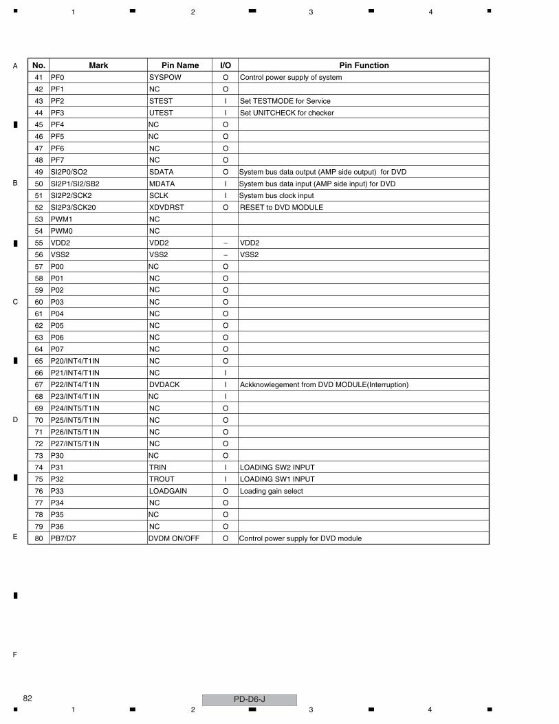
C
D
F
A
B
E
PD-D6-J82
1 2 3 4
No. Mark Pin Name I/O Pin Function41 PF0 O
42 PF1 O
43 PF2 STEST
NC
SYSPOW
I Set TESTMODE for Service
Control power supply of system
44 PF3 UTEST I Set UNITCHECK for checker
45 PF4 NC O
46 PF5 NC O
47 PF6 O
48 PF7 O
49 SI2P0/SO2 SDATA
NC
NC
O System bus data output (AMP side output) for DVD
50 SI2P1/SI2/SB2 MDATA I System bus data input (AMP side input) for DVD
51 SI2P2/SCK2 SCLK I System bus clock input
52 SI2P3/SCK20 XDVDRST O RESET to DVD MODULE
53 PWM1
54 PWM0
55 VDD2 VDD2
NC
NC
− VDD2
56 VSS2 VSS2 − VSS2
57 P00 NC O
58 P01 NC O
59 P02 O
60 P03 NC O
NC
61 P04 NC O
62 P05 NC O
63 P06 O
64 P07 NC O
NC
65 P20/INT4/T1IN NC O
66 P21/INT4/T1IN NC I
67 P22/INT4/T1IN DVDACK I Ackknowlegement from DVD MODULE(Interruption)
68 P23/INT4/T1IN NC I
69 P24/INT5/T1IN NC O
70 P25/INT5/T1IN NC O
71 P26/INT5/T1IN NC O
72 P27/INT5/T1IN NC O
73 P30 NC O
74 P31 TRIN I LOADING SW2 INPUT
75 P32 TROUT I LOADING SW1 INPUT
76 P33 LOADGAIN O Loading gain select
77 P34 NC O
78 P35 NC O
79 P36 NC O
80 PB7/D7 DVDM ON/OFF O Control power supply for DVD module
1 2 3 4
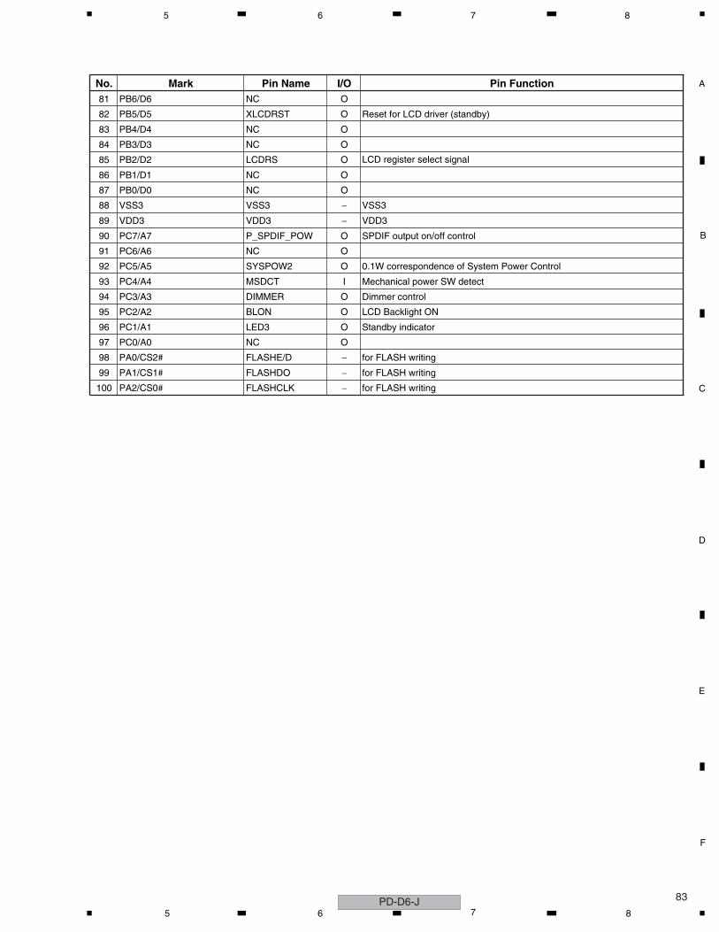
C
D
F
A
B
E
83
5 6 7 8
No. Mark Pin Name I/O Pin Function81 PB6/D6 NC O
82 PB5/D5 XLCDRST O Reset for LCD driver (standby)
LCD register select signal
83 PB4/D4 NC O
84 PB3/D3 NC O
85 PB2/D2 LCDRS O
86 PB1/D1 NC O
87 PB0/D0 NC O
88 VSS3 VSS3 − VSS3
89 VDD3 VDD3 − VDD3
90 PC7/A7 P_SPDIF_POW O SPDIF output on/off control
91 PC6/A6 NC O
92 PC5/A5 SYSPOW2 O 0.1W correspondence of System Power Control
93 PC4/A4 MSDCT I Mechanical power SW detect
94 PC3/A3 DIMMER O Dimmer control
95 PC2/A2 BLON O LCD Backlight ON
96 PC1/A1 LED3 O Standby indicator
97 PC0/A0 NC O
98 PA0/CS2# FLASHE/D − for FLASH writing
99 PA1/CS1# FLASHDO − for FLASH writing
100 PA2/CS0# FLASHCLK − for FLASH writing
PD-D6-J5 6 7 8
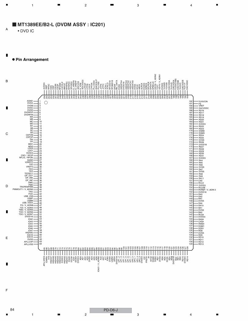
C
D
F
A
B
E
PD-D6-J84
1 2 3 4
MT1389EE/B2-L (DVDM ASSY : IC201)• DVD IC
Pin Arrangement
1
OS
N
2
OS
P
34
DVDRFIP5
DVDRFIN6
MA7
MB8
MC9
MD1011
SB12
SC13
SD14
CDFON15
CDFOP16
TNI17
TPI18
MDI119
MDI220
LDO221
LDO122
V2REFO
23
VREFO
24
V20
25
TEO
26
FEO
272829
HR
FZ
C
30
CR
TP
LP
31
RF
RP
DC
32
RF
RP
AC
3334353637383940414243444546474849505152535455565758596061626364
256
IRE
F25
5R
FG
C25
425
3
RFLVL / RFON
252 251
250
249
248
247
246
245
244
243
242 241
240
239
238
237
236
235
234 233
232 231
230
229 22
822
722
622
522
422
322
222
12
20 219
218
217
216
215
214
213
212
211
210 209
208
207
206
205
204
203
202 201
200 199
198
197 19
619
519
419
3
65 66 67 68 69 70 71
72 73 74 75
76
77
78
79
80
81
82
83
84
85
86
87
88
89
90
91
92
93
94
95 96 97 98 99 100
101
102
103
104
105
106
107
108
109
110
111
112
113
114
115
116
117
118
119
120 121
122
123
124
125
126
127
128
129130131132133134135136137138139140141142143144145146147148149150151152153154155156157158159160161162163164165166167168169170171172173174175176177178179180181182183184185186187188189190191192
SA
DVSS
IOA
1
IOA
0
IOA3IOA4
IOA2
DMO
FG / V_ADIN8
FMO
IOA5IOA6IOA7
APLLVSS
DV
DD
3
DV
DD
3
AD
3
AD
1A
D0
AD
2
HIGHA0
HIG
HA
3
HIG
HA
1H
IGH
A2
HIG
HA
5
AD
6A
D5
AD
7
AD
4
HIG
HA
4
HIG
HA
6H
IGH
A7
A1
6
A17
IOA18IOA19
IOA
20
DV
DD
3U
P3
_5
IOO
E#
INT
0#
UP
1_7
UP
3_4
UP
3_0
RD
4
RD
6
RD
3
RD
2R
D1
RD
0
RWE#CAS#RAS#
RCS#
RD
14
RD13RD12
BA0
RD
15
RD10RD9
RD11
RD
7
DVSS
DV
SS
DV
DD
18
IOC
S#
IOW
R#
UP
1_2
UP
1_3
UP
1_4
UP
1_5
UP
1_6
UP
3_1
UR
D# IR
UW
R#
ALE
RD8
AP
LLV
DD
3
CKERA11
RCLK
DV
SS
RA9RA8
TROFOO
LPF
IN
PL
LV
DD
3
JIT
FN
JIT
FO
LPF
OP
PL
LV
SS
CE
QP
LPF
IPLP
FO
N
TROPENPWMPWMOUT1 / V_ADIN9
YU
V4
/G
YU
V6/
R
YU
V7
PR
ST
#
DV
SS
DV
DD
18
SP
BC
K
DA
CV
SS
B
DA
CV
DD
A
DA
CV
DD
B
DACVDDC
HS
YN
/ V
_A
DIN
2
VS
YN
/ V
_A
DIN
1
USB_VDD3
ICE
XT
AL
IX
TA
LO
YU
V2
/C
YU
V1
/Y
YU
V3
/CV
BS
SP
LR
CK
SP
DA
TA
SP
MC
LK
DA
CV
SS
AY
UV
5/B
AD
CV
SS
AD
CV
DD
3
RA4
RA7
RA6RA5
RD26
DQM1
RA0
DQ
M0
RD30
RA10
RA1RA2RA3
RD31
DVDD18
RD29RD28RD27
RD21
RD25RD24
DQM2
RD22RD23
DQM3
RD18RD19RD20
DVDD18
AB
CK
RD16
AS
DA
TA
2A
SD
AT
A1
DVSS
ALR
CK
AS
DA
TA
0
AC
LK
DVDD3
VREF
DA
CV
SS
C
FSYUV0/CIN
AS
DA
TA
3
AS
DA
TA
4
SP
DIF
MC
_D
AT
A
BA1
DQ
S0
DQS1
RCLKBRVREF / V_ADIN 3
DV
DD
3
DVSS
DVSS
RD
5
DVDD3
DVDD3
DV
SS
DV
SS
DVDD3
AV
DD
3
AGND
SVDD3
SGND
DV
DD
3
CE
QN
RF
VD
D3
RF
GN
D
TEZISLV
CSO / RFOP
USBPUSBM
DVDADVDBDVDCDVDD
DV
DD
3
USB_VSS
IOA
21 /
V_A
DIN
0
DVDD18
DVSS
DVSS
TCK / V_ADIN6TMS / V_ADIN5TDI / V_ADIN4
TDO / V_ADIN7
OP_INP
OP_OUTOP_INN
RD17
DV
DD
18
DV
SS
S_V
RE
FN
IDA
CE
XL
P
S_
VC
M
APLLCAP
RF
VD
D18
RF
GN
D1
8
S_V
RE
FP
1 2 3 4
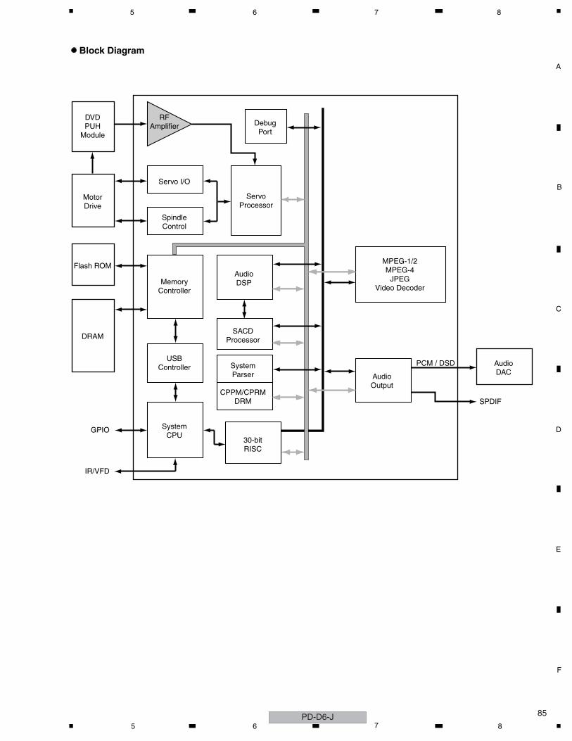
C
D
F
A
B
E
85
5 6 7 8
Block Diagram
DVDPUH
Module
MotorDrive
Servo I/O
ServoProcessor
AudioDSP
AudioOutput
AudioDAC
SPDIF
PCM / DSD
SACDProcessor
SystemParser
CPPM/CPRMDRM
30-bitRISC
DebugPort
MPEG-1/2MPEG-4
JPEGVideo Decoder
SpindleControl
MemoryController
USBController
SystemCPU
Flash ROM
DRAM
GPIO
IR/VFD
RFAmplifier
PD-D6-J5 6 7 8
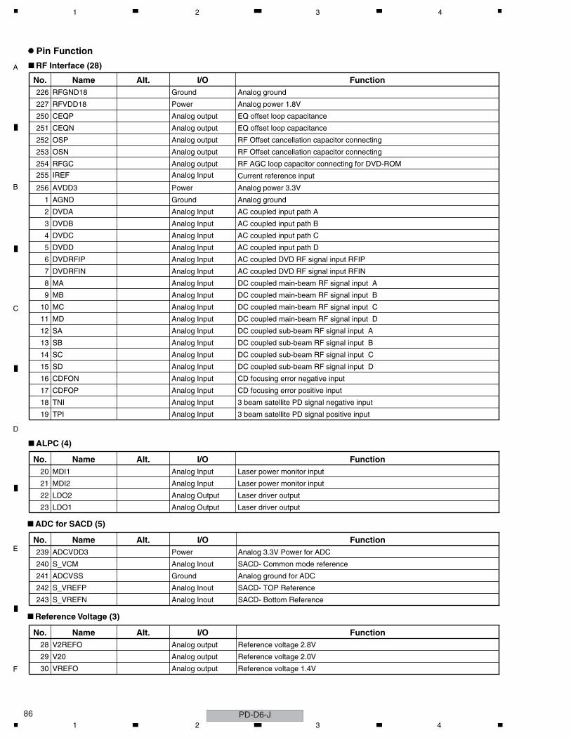
C
D
F
A
B
E
PD-D6-J86
1 2 3 4
Pin Function
RF Interface (28)
ADC for SACD (5)
ALPC (4)
No. Name Alt. I/O Function226 RFGND18 Ground Analog ground
227 RFVDD18 Power Analog power 1.8V
250 CEQP Analog output EQ offset loop capacitance
251 CEQN Analog output EQ offset loop capacitance
252 OSP Analog output RF Offset cancellation capacitor connecting
253 OSN Analog output RF Offset cancellation capacitor connecting
254 RFGC Analog output RF AGC loop capacitor connecting for DVD-ROM
255 IREF Analog Input Current reference input
256 AVDD3 Power Analog power 3.3V
1 AGND Ground Analog ground
2 DVDA Analog Input AC coupled input path A
3 DVDB Analog Input AC coupled input path B
4 DVDC Analog Input AC coupled input path C
5 DVDD Analog Input AC coupled input path D
6 DVDRFIP Analog Input AC coupled DVD RF signal input RFIP
7 DVDRFIN Analog Input AC coupled DVD RF signal input RFIN
8 MA Analog Input DC coupled main-beam RF signal input A
9 MB Analog Input DC coupled main-beam RF signal input B
10 MC Analog Input DC coupled main-beam RF signal input C
11 MD Analog Input DC coupled main-beam RF signal input D
12 SA Analog Input DC coupled sub-beam RF signal input A
13 SB Analog Input DC coupled sub-beam RF signal input B
14 SC Analog Input DC coupled sub-beam RF signal input C
15 SD Analog Input DC coupled sub-beam RF signal input D
16 CDFON Analog Input CD focusing error negative input
17 CDFOP Analog Input CD focusing error positive input
18 TNI Analog Input 3 beam satellite PD signal negative input
19 TPI Analog Input 3 beam satellite PD signal positive input
No. Name Alt. I/O Function20 MDI1 Analog Input Laser power monitor input
21 MDI2 Analog Input Laser power monitor input
22 LDO2 Analog Output Laser driver output
23 LDO1 Analog Output Laser driver output
No. Name Alt. I/O Function239 ADCVDD3 Power Analog 3.3V Power for ADC
240 S_VCM Analog Inout SACD- Common mode reference
241 ADCVSS Ground Analog ground for ADC
242 S_VREFP Analog Inout SACD- TOP Reference
243 S_VREFN Analog Inout SACD- Bottom Reference
Reference Voltage (3)
No. Name Alt. I/O Function28 V2REFO Analog output Reference voltage 2.8V
29 V20 Analog output Reference voltage 2.0V
30 VREFO Analog output Reference voltage 1.4V
1 2 3 4
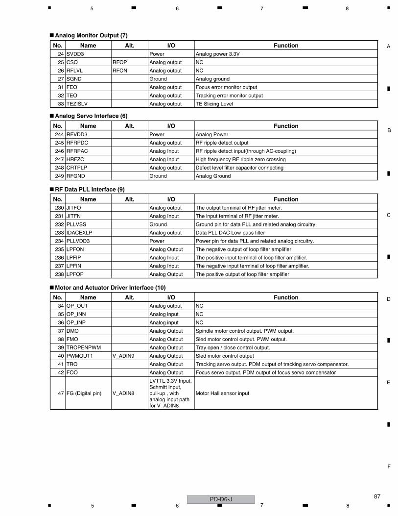
C
D
F
A
B
E
87
5 6 7 8
Motor and Actuator Driver Interface (10)
RF Data PLL Interface (9)
Analog Monitor Output (7)
No. Name Alt. I/O Function24 SVDD3 Power Analog power 3.3V
25 CSO RFOP Analog output NC
26 RFLVL RFON Analog output NC
27 SGND Ground Analog ground
31 FEO Analog output Focus error monitor output
32 TEO Analog output Tracking error monitor output
33 TEZISLV Analog output TE Slicing Level
Analog Servo Interface (6)
No. Name Alt. I/O Function244 RFVDD3 Power Analog Power
245 RFRPDC Analog output RF ripple detect output
246 RFRPAC Analog Input RF ripple detect input(through AC-coupling)
247 HRFZC Analog Input High frequency RF ripple zero crossing
248 CRTPLP Analog output Defect level filter capacitor connecting
249 RFGND Ground Analog Ground
No. Name Alt. I/O Function230 JITFO Analog output The output terminal of RF jitter meter.
231 JITFN Analog Input The input terminal of RF jitter meter.
232 PLLVSS Ground Ground pin for data PLL and related analog circuitry.
233 IDACEXLP Analog output Data PLL DAC Low-pass filter
234 PLLVDD3 Power Power pin for data PLL and related analog circuitry.
235 LPFON Analog Output The negative output of loop filter amplifier
236 LPFIP Analog Input The positive input terminal of loop filter amplifier.
237 LPFIN Analog Input The negative input terminal of loop filter amplifier.
238 LPFOP Analog Output The positive output of loop filter amplifier
No. Name Alt. I/O Function34 OP_OUT Analog output NC
35 OP_INN Analog input NC
36 OP_INP Analog input NC
37 DMO Analog Output Spindle motor control output. PWM output.
38 FMO Analog Output Sled motor control output. PWM output.
39 TROPENPWM Analog Output Tray open / close control output.
40 PWMOUT1 V_ADIN9 Analog Output Sled motor control output
41 TRO Analog Output Tracking servo output. PDM output of tracking servo compensator.
42 FOO Analog Output Focus servo output. PDM output of focus servo compensator
47 FG (Digital pin) V_ADIN8
LVTTL 3.3V Input, Schmitt Input, pull-up , with analog input path for V_ADIN8
Motor Hall sensor input
PD-D6-J5 6 7 8
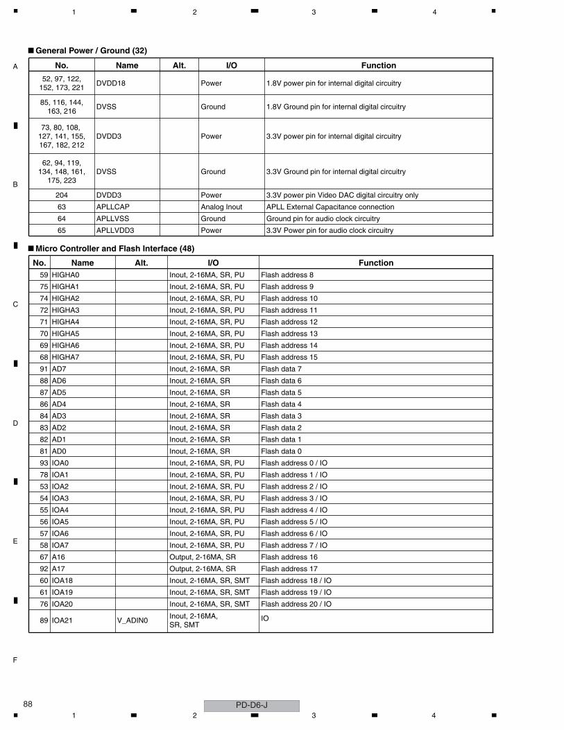
C
D
F
A
B
E
PD-D6-J88
1 2 3 4
Micro Controller and Flash Interface (48)
General Power / Ground (32)
No. Name Alt. I/O Function
52, 97, 122,152, 173, 221
DVDD18 Power 1.8V power pin for internal digital circuitry
85, 116, 144,163, 216
DVSS Ground 1.8V Ground pin for internal digital circuitry
73, 80, 108, 127, 141, 155,167, 182, 212
DVDD3 Power 3.3V power pin for internal digital circuitry
62, 94, 119,134, 148, 161,
175, 223DVSS Ground 3.3V Ground pin for internal digital circuitry
204 DVDD3 Power 3.3V power pin Video DAC digital circuitry only
63 APLLCAP Analog Inout APLL External Capacitance connection
64 APLLVSS Ground Ground pin for audio clock circuitry
65 APLLVDD3 Power 3.3V Power pin for audio clock circuitry
No. Name Alt. I/O Function59 HIGHA0 Inout, 2-16MA, SR, PU Flash address 8
75 HIGHA1 Inout, 2-16MA, SR, PU Flash address 9
74 HIGHA2 Inout, 2-16MA, SR, PU Flash address 10
72 HIGHA3 Inout, 2-16MA, SR, PU Flash address 11
71 HIGHA4 Inout, 2-16MA, SR, PU Flash address 12
70 HIGHA5 Inout, 2-16MA, SR, PU Flash address 13
69 HIGHA6 Inout, 2-16MA, SR, PU Flash address 14
68 HIGHA7 Inout, 2-16MA, SR, PU Flash address 15
91 AD7 Inout, 2-16MA, SR Flash data 7
88 AD6 Inout, 2-16MA, SR Flash data 6
87 AD5 Inout, 2-16MA, SR Flash data 5
86 AD4 Inout, 2-16MA, SR Flash data 4
84 AD3 Inout, 2-16MA, SR Flash data 3
83 AD2 Inout, 2-16MA, SR Flash data 2
82 AD1 Inout, 2-16MA, SR Flash data 1
81 AD0 Inout, 2-16MA, SR Flash data 0
93 IOA0 Inout, 2-16MA, SR, PU Flash address 0 / IO
78 IOA1 Inout, 2-16MA, SR, PU Flash address 1 / IO
53 IOA2 Inout, 2-16MA, SR, PU Flash address 2 / IO
54 IOA3 Inout, 2-16MA, SR, PU Flash address 3 / IO
55 IOA4 Inout, 2-16MA, SR, PU Flash address 4 / IO
56 IOA5 Inout, 2-16MA, SR, PU Flash address 5 / IO
57 IOA6 Inout, 2-16MA, SR, PU Flash address 6 / IO
58 IOA7 Inout, 2-16MA, SR, PU Flash address 7 / IO
67 A16 Output, 2-16MA, SR Flash address 16
92 A17 Output, 2-16MA, SR Flash address 17
60 IOA18 Inout, 2-16MA, SR, SMT Flash address 18 / IO
61 IOA19 Inout, 2-16MA, SR, SMT Flash address 19 / IO
76 IOA20 Inout, 2-16MA, SR, SMT Flash address 20 / IO
89 IOA21 V_ADIN0Inout, 2-16MA,SR, SMT
IO
1 2 3 4
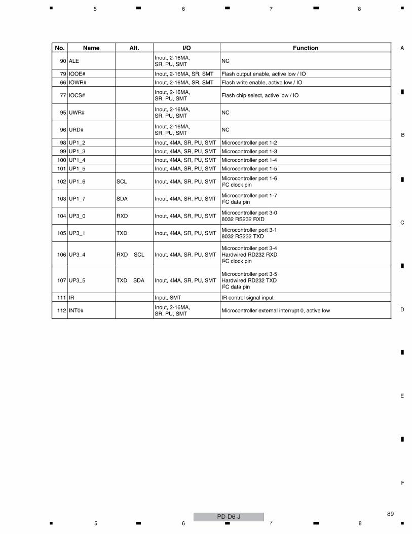
C
D
F
A
B
E
89
5 6 7 8
No. Name Alt. I/O Function
90 ALEInout, 2-16MA,SR, PU, SMT
NC
79 IOOE# Inout, 2-16MA, SR, SMT Flash output enable, active low / IO
66 IOWR# Inout, 2-16MA, SR, SMT Flash write enable, active low / IO
77 IOCS#Inout, 2-16MA,SR, PU, SMT
Flash chip select, active low / IO
95 UWR#Inout, 2-16MA,SR, PU, SMT
NC
96 URD#Inout, 2-16MA,SR, PU, SMT
NC
98 UP1_2 Inout, 4MA, SR, PU, SMT Microcontroller port 1-2
99 UP1_3 Inout, 4MA, SR, PU, SMT Microcontroller port 1-3
100 UP1_4 Inout, 4MA, SR, PU, SMT Microcontroller port 1-4
101 UP1_5 Inout, 4MA, SR, PU, SMT Microcontroller port 1-5
102 UP1_6 SCL Inout, 4MA, SR, PU, SMTMicrocontroller port 1-6I2C clock pin
103 UP1_7 SDA Inout, 4MA, SR, PU, SMTMicrocontroller port 1-7I2C data pin
104 UP3_0 RXD Inout, 4MA, SR, PU, SMTMicrocontroller port 3-08032 RS232 RXD
105 UP3_1 TXD Inout, 4MA, SR, PU, SMTMicrocontroller port 3-18032 RS232 TXD
106 UP3_4 RXD SCL Inout, 4MA, SR, PU, SMTMicrocontroller port 3-4Hardwired RD232 RXDI2C clock pin
107 UP3_5 TXD SDA Inout, 4MA, SR, PU, SMTMicrocontroller port 3-5Hardwired RD232 TXDI2C data pin
111 IR Input, SMT IR control signal input
112 INT0#Inout, 2-16MA,SR, PU, SMT
Microcontroller external interrupt 0, active low
PD-D6-J5 6 7 8
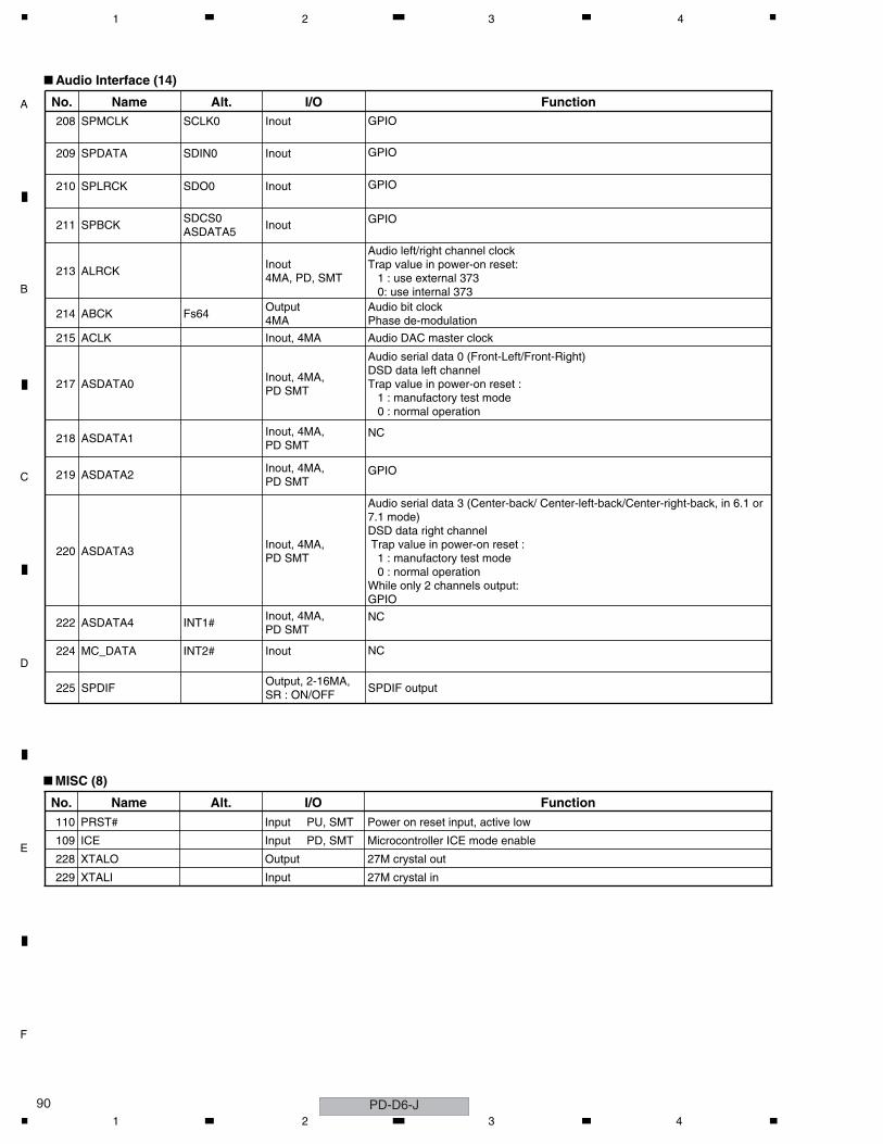
C
D
F
A
B
E
PD-D6-J90
1 2 3 4
Audio Interface (14)
No. Name Alt. I/O Function208 SPMCLK SCLK0 Inout GPIO
209 SPDATA SDIN0 Inout GPIO
210 SPLRCK SDO0 Inout GPIO
211 SPBCKSDCS0ASDATA5
Inout GPIO
213 ALRCKInout4MA, PD, SMT
Audio left/right channel clockTrap value in power-on reset: 1 : use external 373 0: use internal 373
214 ABCK Fs64Output4MA
Audio bit clockPhase de-modulation
215 ACLK Inout, 4MA Audio DAC master clock
217 ASDATA0Inout, 4MA,PD SMT
Audio serial data 0 (Front-Left/Front-Right)DSD data left channelTrap value in power-on reset : 1 : manufactory test mode 0 : normal operation
218 ASDATA1Inout, 4MA,PD SMT
NC
219 ASDATA2Inout, 4MA,PD SMT
GPIO
220 ASDATA3Inout, 4MA,PD SMT
Audio serial data 3 (Center-back/ Center-left-back/Center-right-back, in 6.1 or 7.1 mode)DSD data right channel Trap value in power-on reset : 1 : manufactory test mode 0 : normal operationWhile only 2 channels output:GPIO
222 ASDATA4 INT1#Inout, 4MA,PD SMT
NC
224 MC_DATA INT2# Inout NC
225 SPDIFOutput, 2-16MA,SR : ON/OFF
SPDIF output
MISC (8)
No. Name Alt. I/O Function110 PRST# Input PU, SMT Power on reset input, active low
109 ICE Input PD, SMT Microcontroller ICE mode enable
228 XTALO Output 27M crystal out
229 XTALI Input 27M crystal in
1 2 3 4
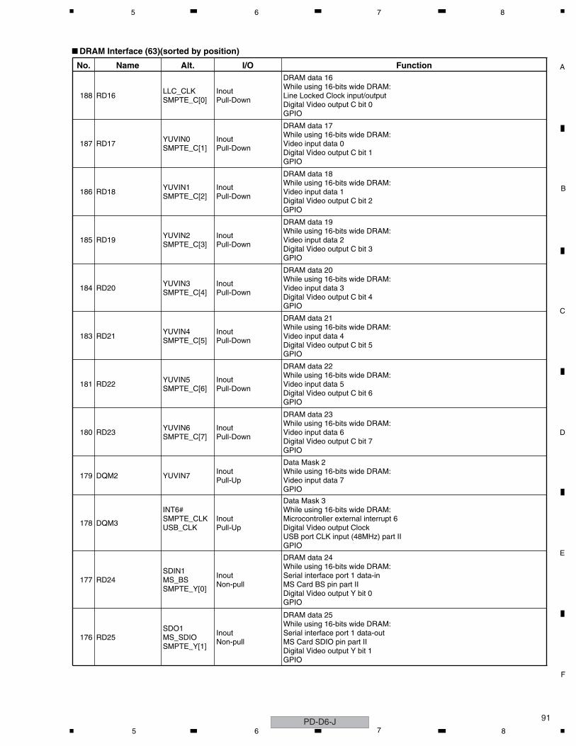
C
D
F
A
B
E
91
5 6 7 8
DRAM Interface (63)(sorted by position)
No. Name Alt. I/O Function
188 RD16LLC_CLK SMPTE_C[0]
InoutPull-Down
DRAM data 16While using 16-bits wide DRAM:Line Locked Clock input/outputDigital Video output C bit 0GPIO
187 RD17YUVIN0 SMPTE_C[1]
InoutPull-Down
DRAM data 17While using 16-bits wide DRAM:Video input data 0Digital Video output C bit 1GPIO
186 RD18YUVIN1 SMPTE_C[2]
InoutPull-Down
DRAM data 18While using 16-bits wide DRAM:Video input data 1Digital Video output C bit 2GPIO
185 RD19YUVIN2 SMPTE_C[3]
InoutPull-Down
DRAM data 19While using 16-bits wide DRAM:Video input data 2Digital Video output C bit 3GPIO
184 RD20YUVIN3 SMPTE_C[4]
InoutPull-Down
DRAM data 20While using 16-bits wide DRAM:Video input data 3Digital Video output C bit 4GPIO
183 RD21YUVIN4 SMPTE_C[5]
InoutPull-Down
DRAM data 21While using 16-bits wide DRAM:Video input data 4Digital Video output C bit 5GPIO
181 RD22YUVIN5 SMPTE_C[6]
InoutPull-Down
DRAM data 22While using 16-bits wide DRAM:Video input data 5Digital Video output C bit 6GPIO
180 RD23YUVIN6 SMPTE_C[7]
InoutPull-Down
DRAM data 23While using 16-bits wide DRAM:Video input data 6Digital Video output C bit 7GPIO
179 DQM2 YUVIN7InoutPull-Up
Data Mask 2While using 16-bits wide DRAM:Video input data 7GPIO
178 DQM3
INT6# SMPTE_CLK USB_CLK
InoutPull-Up
Data Mask 3While using 16-bits wide DRAM:Microcontroller external interrupt 6Digital Video output ClockUSB port CLK input (48MHz) part IIGPIO
177 RD24SDIN1 MS_BS SMPTE_Y[0]
InoutNon-pull
DRAM data 24While using 16-bits wide DRAM:Serial interface port 1 data-inMS Card BS pin part IIDigital Video output Y bit 0GPIO
176 RD25SDO1 MS_SDIO SMPTE_Y[1]
InoutNon-pull
DRAM data 25While using 16-bits wide DRAM:Serial interface port 1 data-outMS Card SDIO pin part IIDigital Video output Y bit 1GPIO
PD-D6-J5 6 7 8
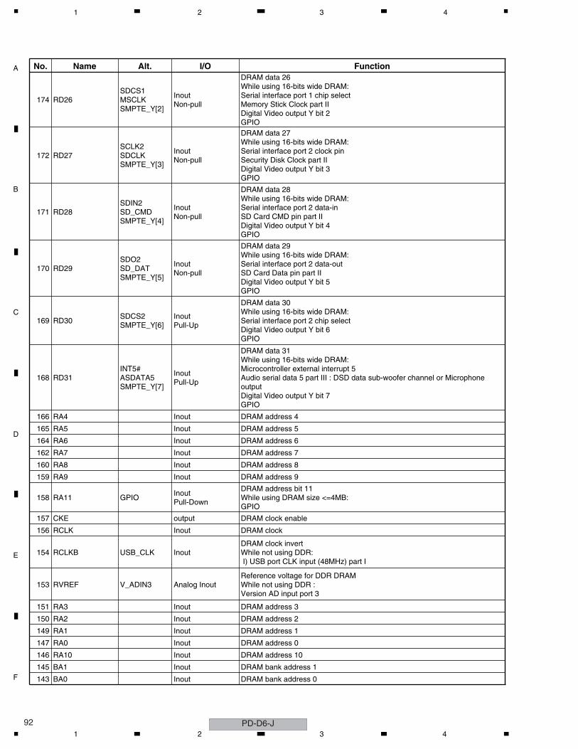
C
D
F
A
B
E
PD-D6-J92
1 2 3 4
No. Name Alt. I/O Function
174 RD26SDCS1 MSCLK SMPTE_Y[2]
InoutNon-pull
DRAM data 26While using 16-bits wide DRAM:Serial interface port 1 chip select Memory Stick Clock part IIDigital Video output Y bit 2GPIO
172 RD27SCLK2 SDCLK SMPTE_Y[3]
InoutNon-pull
DRAM data 27While using 16-bits wide DRAM:Serial interface port 2 clock pinSecurity Disk Clock part IIDigital Video output Y bit 3GPIO
171 RD28SDIN2 SD_CMD SMPTE_Y[4]
InoutNon-pull
DRAM data 28While using 16-bits wide DRAM:Serial interface port 2 data-inSD Card CMD pin part IIDigital Video output Y bit 4GPIO
170 RD29SDO2 SD_DAT SMPTE_Y[5]
InoutNon-pull
DRAM data 29While using 16-bits wide DRAM:Serial interface port 2 data-outSD Card Data pin part IIDigital Video output Y bit 5GPIO
169 RD30SDCS2 SMPTE_Y[6]
InoutPull-Up
DRAM data 30While using 16-bits wide DRAM:Serial interface port 2 chip selectDigital Video output Y bit 6GPIO
168 RD31INT5# ASDATA5 SMPTE_Y[7]
InoutPull-Up
DRAM data 31While using 16-bits wide DRAM:Microcontroller external interrupt 5Audio serial data 5 part III : DSD data sub-woofer channel or Microphone outputDigital Video output Y bit 7GPIO
166 RA4 Inout DRAM address 4
165 RA5 Inout DRAM address 5
164 RA6 Inout DRAM address 6
162 RA7 Inout DRAM address 7
160 RA8 Inout DRAM address 8
159 RA9 Inout DRAM address 9
158 RA11 GPIOInoutPull-Down
DRAM address bit 11While using DRAM size <=4MB:GPIO
157 CKE output DRAM clock enable
156 RCLK Inout DRAM clock
154 RCLKB USB_CLK InoutDRAM clock invertWhile not using DDR: I) USB port CLK input (48MHz) part I
153 RVREF V_ADIN3 Analog InoutReference voltage for DDR DRAMWhile not using DDR :Version AD input port 3
151 RA3 Inout DRAM address 3
150 RA2 Inout DRAM address 2
149 RA1 Inout DRAM address 1
147 RA0 Inout DRAM address 0
146 RA10 Inout DRAM address 10
145 BA1 Inout DRAM bank address 1
143 BA0 Inout DRAM bank address 0
1 2 3 4
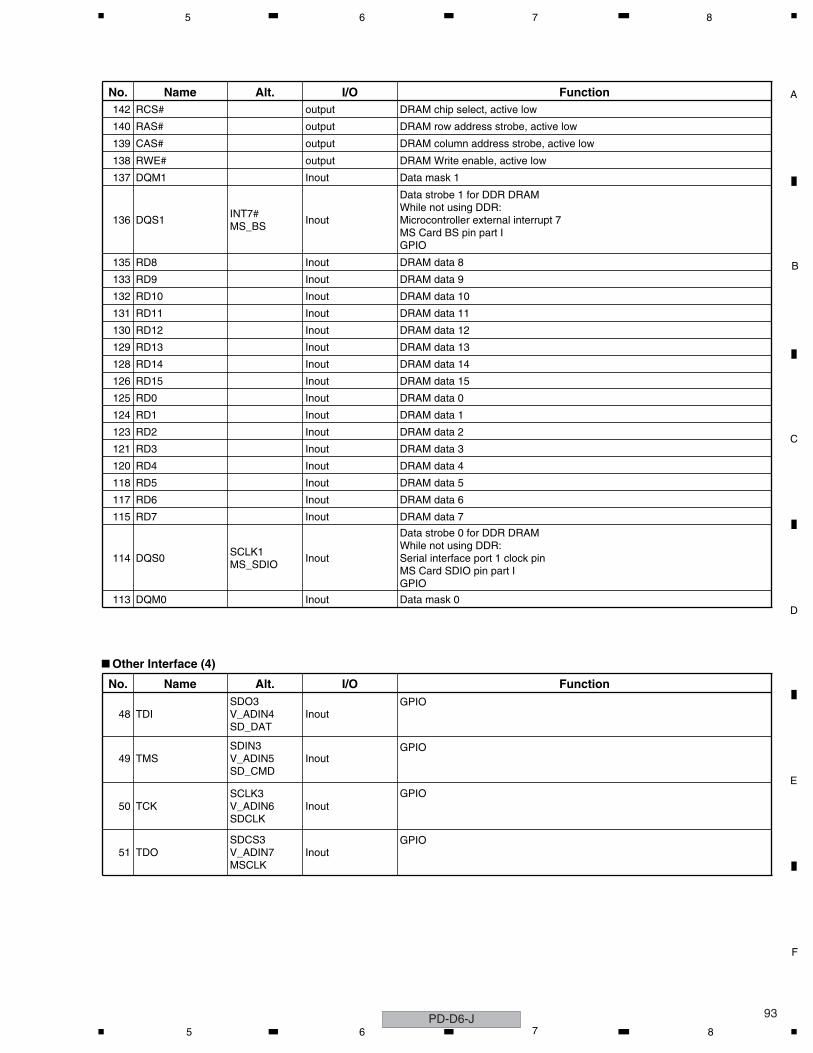
C
D
F
A
B
E
93
5 6 7 8
No. Name Alt. I/O Function142 RCS# output DRAM chip select, active low
140 RAS# output DRAM row address strobe, active low
139 CAS# output DRAM column address strobe, active low
138 RWE# output DRAM Write enable, active low
137 DQM1 Inout Data mask 1
136 DQS1INT7# MS_BS
Inout
Data strobe 1 for DDR DRAMWhile not using DDR:Microcontroller external interrupt 7MS Card BS pin part IGPIO
135 RD8 Inout DRAM data 8
133 RD9 Inout DRAM data 9
132 RD10 Inout DRAM data 10
131 RD11 Inout DRAM data 11
130 RD12 Inout DRAM data 12
129 RD13 Inout DRAM data 13
128 RD14 Inout DRAM data 14
126 RD15 Inout DRAM data 15
125 RD0 Inout DRAM data 0
124 RD1 Inout DRAM data 1
123 RD2 Inout DRAM data 2
121 RD3 Inout DRAM data 3
120 RD4 Inout DRAM data 4
118 RD5 Inout DRAM data 5
117 RD6 Inout DRAM data 6
115 RD7 Inout DRAM data 7
114 DQS0SCLK1 MS_SDIO
Inout
Data strobe 0 for DDR DRAMWhile not using DDR:Serial interface port 1 clock pinMS Card SDIO pin part IGPIO
113 DQM0 Inout Data mask 0
Other Interface (4)
No. Name Alt. I/O Function
48 TDISDO3 V_ADIN4 SD_DAT
InoutGPIO
49 TMSSDIN3 V_ADIN5 SD_CMD
InoutGPIO
50 TCKSCLK3 V_ADIN6 SDCLK
InoutGPIO
51 TDOSDCS3 V_ADIN7 MSCLK
InoutGPIO
PD-D6-J5 6 7 8
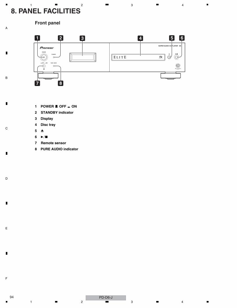
C
D
F
A
B
E
PD-D6-J94
1 2 3 4
8. PANEL FACILITIES
Front panel
1 POWER OFF ON
2 STANDBY indicator
3 Display
4 Disc tray
5
6 /
7 Remote sensor
8 PURE AUDIO indicator
3 41
7
2 5 6
8
1 2 3 4
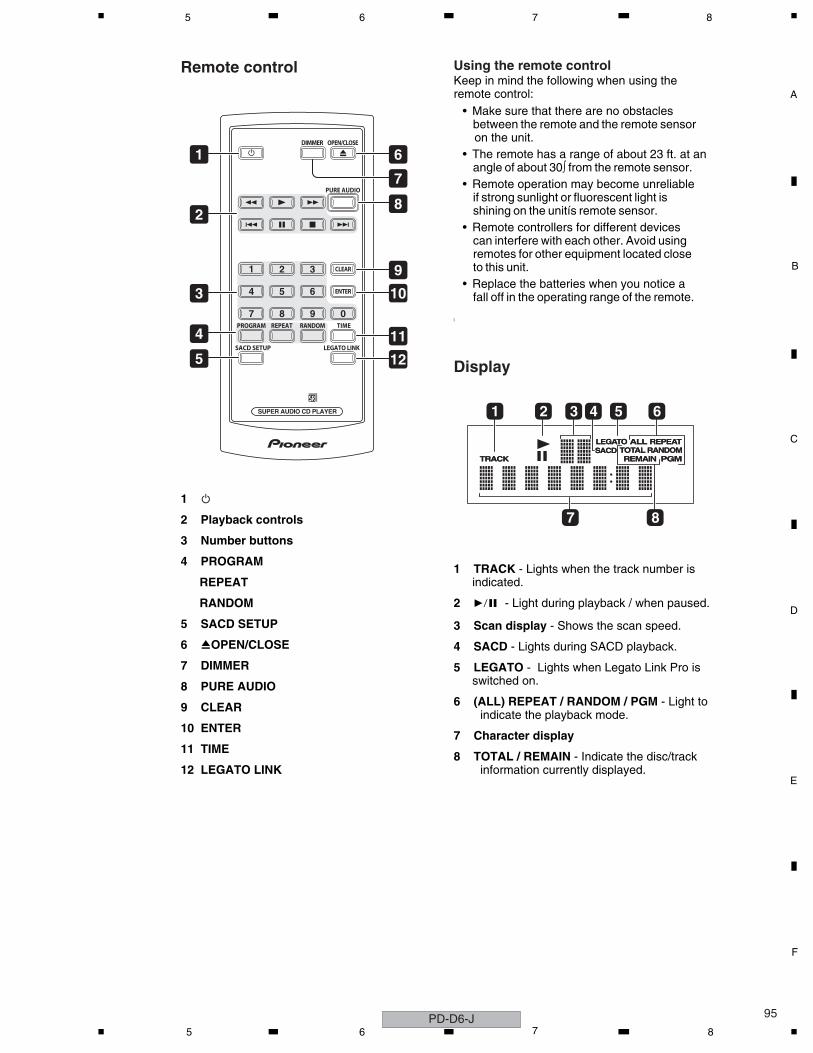
C
D
F
A
B
E
95
5 6 7 8
Remote control
1
2 Playback controls
3 Number buttons
4 PROGRAM
REPEAT
RANDOM
5 SACD SETUP
6 OPEN/CLOSE
7 DIMMER
8 PURE AUDIO
9 CLEAR
10 ENTER
11 TIME
12 LEGATO LINK
Using the remote controlKeep in mind the following when using the remote control: Make sure that there are no obstacles between the remote and the remote sensor on the unit. The remote has a range of about 23 ft. at an angle of about 30∫ from the remote sensor. Remote operation may become unreliable if strong sunlight or fluorescent light is shining on the unitís remote sensor. Remote controllers for different devices can interfere with each other. Avoid using remotes for other equipment located close to this unit. Replace the batteries when you notice a fall off in the operating range of the remote.
Display
1 TRACK - Lights when the track number is indicated.
2 - Light during playback / when paused.
3 Scan display - Shows the scan speed.
4 SACD - Lights during SACD playback.
5 LEGATO - Lights when Legato Link Pro is switched on.
6 (ALL) REPEAT / RANDOM / PGM - Light to indicate the playback mode.
7 Character display
8 TOTAL / REMAIN - Indicate the disc/track information currently displayed.
1
2
3
4
5
6
7
8
11
12
9
10
LEGATO ALLTOTAL
REPEAT
PGMREMAINRANDOM
TRACKSACD
1 2 3 4 5 6
7 8
PD-D6-J5 6 7 8
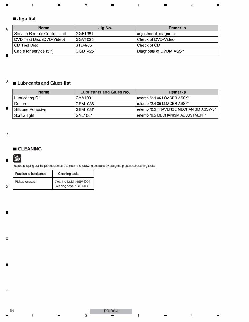
C
D
F
A
B
E
PD-D6-J96
1 2 3 4
Service Remote Control Unit GGF1381DVD Test Disc (DVD-Video) GGV1025
adjustment, diagnosisName Jig No. Remarks
Check of DVD-VideoCD Test Disc STD-905 Check of CDCable for service (5P) GGD1425 Diagnosis of DVDM ASSY
7 Jigs list
Lubricating Oil GYA1001
GEM1036Daifree
Name Lubricants and Glues No. Remarks
refer to "2.4 05 LOADER ASSY"
refer to "2.4 05 LOADER ASSY"
GEM1037Silicone Adhesive refer to "2.5 TRAVERSE MECHANISM ASSY-S"
7 Lubricants and Glues list
GYL1001Screw tight refer to "6.5 MECHANISM ADJUSTMENT"
Before shipping out the product, be sure to clean the following positions by using the prescribed cleaning tools:
Position to be cleaned Cleaning tools
Pickup leneses Cleaning liquid : GEM1004Cleaning paper : GED-008
7 CLEANING
1 2 3 4