studies on the growth, structural and electrical...
TRANSCRIPT
STUDIES ON THE GROWTH, STRUCTURAL AND ELECTRICAL PROPERTIES OF SILICON-BASED
HETEROSTRUCTURE NANOWIRES
QIAN GUANGHAN
FACULTY OF SCIENCE UNIVERSITY OF MALAYA
KUALA LUMPUR 2015
STUDIES ON THE GROWTH, STRUCTURAL AND ELECTRICAL PROPERTIES OF SILICON-BASED
HETEROSTRUCTURE NANOWIRES
QIAN GUANGHAN
DISSERTATION SUBMITTED IN FULFILMENT OF THE REQUIREMENTS
FOR THE DEGGREE OF MASTER SCIENCE
FACULTY OF SCIENCE UNIVERSITY OF MALAYA
KUALA LUMPUR 2015
ii
UNIVERSITI MALAYA
ORIGINAL LITERARY WORK DECLARATION
Name of Candidate: QIAN GUANGHAN
I/C/Passport No: G42001151
Regisration/Matric No.: SGG130002
Name of Degree: MASTER OF TECHNOLOGY (MATERIALS SCIENCE)
Title of Project Paper/Research Report/Dissertation/Thesis (“this Work”):
“STUDIES ON THE GROWTH, STRUCTURAL AND ELECTRICAL PROPERTIES OF SILICON-BASED HETEROSTRUCTURE NANOWIRES”
Field of Study: NANOTECHNOLOGY AND NANOMATERIALS
I do solemnly and sincerely declare that:
(1) I am the sole author/writer of this Work, (2) This Work is original, (3) Any use of any work in which copyright exists was done by way of fair dealing and for
permitted purposes and any excerpt or extract from, or reference to or reproduction of any copyright work has been disclosed expressly and sufficiently and the title of the Work and its authorship have been acknowledged in this Work,
(4) I do not have any actual knowledge nor do I ought reasonably to know that the making of this work constitutes an infringement of any copyright work,
(5) I hereby assign all and every rights in the copyright to this Work to the University of Malaya (“UM”), who henceforth shall be owner of the copyright in this Work and that any reproduction or use in any form or by any means whatsoever is prohibited without the written consent of UM having been first had and obtained,
(6) I am fully aware that if in the course of making this Work I have infringed any copyright whether intentionally or otherwise, I may be subject to legal action or any other action as may be determined by UM.
(Candidate Signature) Date:
Subscribed and solemnly declared before,
Witness’s Signature Date:
Name:
Designation:
iii
ABSTRACT
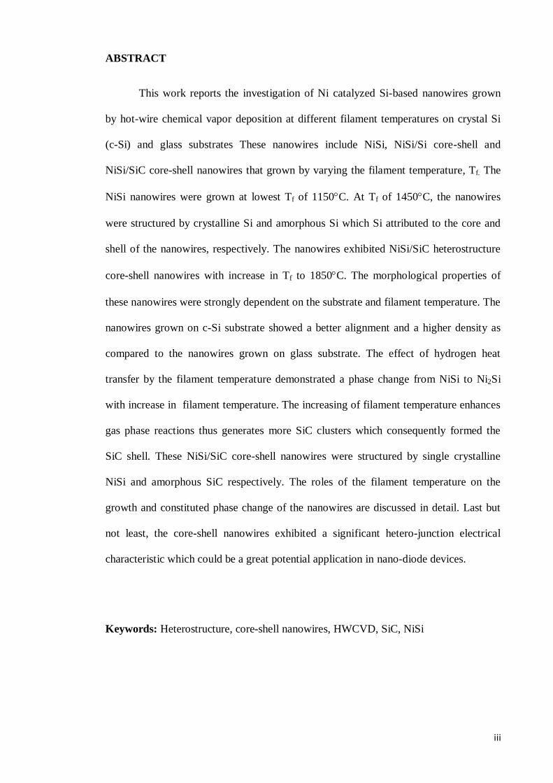
This work reports the investigation of Ni catalyzed Si-based nanowires grown
by hot-wire chemical vapor deposition at different filament temperatures on crystal Si
(c-Si) and glass substrates These nanowires include NiSi, NiSi/Si core-shell and
NiSi/SiC core-shell nanowires that grown by varying the filament temperature, Tf. The
NiSi nanowires were grown at lowest Tf of 1150C. At Tf of 1450C, the nanowires
were structured by crystalline Si and amorphous Si which Si attributed to the core and
shell of the nanowires, respectively. The nanowires exhibited NiSi/SiC heterostructure
core-shell nanowires with increase in Tf to 1850C. The morphological properties of
these nanowires were strongly dependent on the substrate and filament temperature. The
nanowires grown on c-Si substrate showed a better alignment and a higher density as
compared to the nanowires grown on glass substrate. The effect of hydrogen heat
transfer by the filament temperature demonstrated a phase change from NiSi to Ni2Si
with increase in filament temperature. The increasing of filament temperature enhances
gas phase reactions thus generates more SiC clusters which consequently formed the
SiC shell. These NiSi/SiC core-shell nanowires were structured by single crystalline
NiSi and amorphous SiC respectively. The roles of the filament temperature on the
growth and constituted phase change of the nanowires are discussed in detail. Last but
not least, the core-shell nanowires exhibited a significant hetero-junction electrical
characteristic which could be a great potential application in nano-diode devices.
Keywords: Heterostructure, core-shell nanowires, HWCVD, SiC, NiSi
iv
ABSTRAK
Ni-bermangkin Si berasaskan heterostruktur nanowayar ditumbuh di atas kristal
Si substrat oleh wayar panas wap kimia pemendapan (HWCVD) telah dikaji. Ini
termasuk heterostruktur nanowayar NiSi, amorfus/kristal Si nanowayar teras-tempurung
dan NiSi/SiC nanowayar teras-tempurung yang berkembang dengan mengubah suhu
filamen, Tf. Pada Tf 1450C, heterostruktur nanowayar terbentuk oleh kristal dan
amorfus Si yang berpunca daripada teras dan tempurung nanowayar masing-masing.
Morfologi nanowayar menunjukkan perubahan ketara dengan peningkatan suhu filamen.
Selain itu, pemindahan haba hidrogen oleh suhu filamen menunjukkan perubahan fasa
dari NiSi kepada Ni2Si dengan peningkatan suhu filamen. Peningkatan suhu filamen
juga meningkatkan tindak balas fasa gas yang menjana lebih banyak kelompok SiC dan
seterusnya membentuk NiSi/SiC nanowayar teras-tempurung pada 1850C. Peranan
suhu filamen pada pertumbuhan dan perubahan fasa nanowayar turut dibincangkan.
Ciri-ciri elektrik yang terdapat pada nanowayar turut dipersembahkan.
Kata Kunci: Heterostruktur nanowayar, Wayar panas wap kimia pemendapan
(HWCVD), pertumbuhan Nanowayar.
v
ACKNOWLEDGEMENT
I would like to express my sincere gratitude and thanks to my supervisor, Dr.
Goh Boon Tong for guiding and advising me throughout this work. Profuse thanks to
him for being patient and understanding. Without his criticism, comments, timely aid
and intervention this study may not have materialized.
Also, I would like to thank all the members of Low Dimensional Materials
Research Centre, Department of Physics in University of Malaya members for guiding
me, giving suggestions, ideas, and support. Among them includes Nur Fatin Farhanah
binti Nazaruddin, Najwa binti Hamzan and Farah Nadiah binti Nordin. The experiences
with them have been wonderful, interesting and rewarding.
This work was supported by the University of Malaya Research Grant (UMRG)
of RG259-13AFR and the University of Malaya Postgraduate Research Fund (PPP) of
PO032-2014A.
vi
TABLE OF CONTENTS
Page
Abstract iii
Acknowledgement v
Table of Contents vi
List of Figures viii
List of Tables xii
List of Symbols and Abbreviations xiii
Chapter 1 INTRODUCTION
1.1 Background 1
1.2 Problem statement 6
1.3 Motivation of this work 7
1.4 Objectives 7
1.5 Thesis overview 8
Chapter 2 LITERATURE REVIEW
2.1 Nanomaterials and nanotechnology 9
2.2 One-dimensional NiSi and SiC nanowire 10
2.3 Nanowire diode 19
2.3 Hot-wire chemical vapor deposition (HWCVD) 19
2.4 Nanowire grow mechanism 24
Chapter 3 METHODOLOGY
3.1 Introduction 31
3.2 Hot-wire chemical vapour deposition
3.2.1 Vacuum chamber
3.2.2 Plasma generator
3.2.3 Hot-wire supply
3.2.4 Vacuum system
3.2.5 Gas supply
3.2.6 Heating supply
31
33
33
34
35
36
37
vii
3.3 Experiment method
3.3.1 Substrate cleaning
3.3.2 Pre-heating of filament
3.3.3 Ni evaporation
3.3.4 Deposition
38
38
39
40
41
3.4 Characterization techniques 43
3.4.1 Scanning electron microscope (SEM) 43
3.4.2 Energy dispersive X-ray (EDX) 43
3.4.3 Transmission electron microscope (TEM) 44
3.4.4 X-ray diffraction (XRD) 46
3.4.5 Raman spectroscopy 47
3.4.5 I-V measurement 48
Chapter 4 RESULTS AND DISCUSSIONS
4.1 Effects of filament temperature on substrate surface
temperature
50
4.2 Surface morphologies of nanowires 51
4.3 Cross-sectional view study 56
4.4 Microstructure study 59
4.5 Compositions studies of a single nanowire by EDS
elemental mappings
62
4.6 Phases and orientation studies 63
4.7 Structural properties study 67
4.8 Optical properties study by photoluminescence
emission spectra
69
4.9 Electrical properties study 71
Chapter 5 CONCLUSIONS
5.1 Conclusions 75
REFERENCES 77
viii
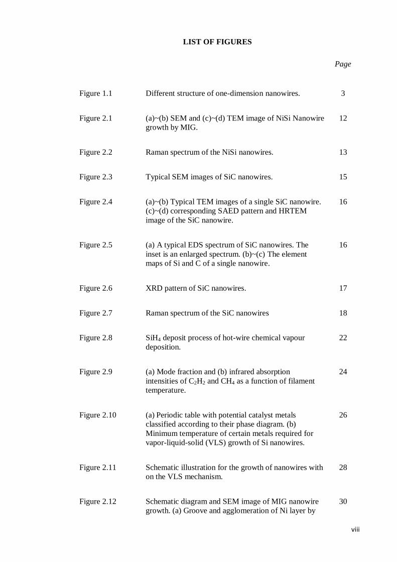
LIST OF FIGURES
Page
Figure 1.1 Different structure of one-dimension nanowires. 3
Figure 2.1 (a)~(b) SEM and (c)~(d) TEM image of NiSi Nanowire
growth by MIG.
12
Figure 2.2 Raman spectrum of the NiSi nanowires. 13
Figure 2.3 Typical SEM images of SiC nanowires. 15
Figure 2.4 (a)~(b) Typical TEM images of a single SiC nanowire.
(c)~(d) corresponding SAED pattern and HRTEM
image of the SiC nanowire.
16
Figure 2.5 (a) A typical EDS spectrum of SiC nanowires. The
inset is an enlarged spectrum. (b)~(c) The element
maps of Si and C of a single nanowire.
16
Figure 2.6 XRD pattern of SiC nanowires. 17
Figure 2.7 Raman spectrum of the SiC nanowires 18
Figure 2.8 SiH4 deposit process of hot-wire chemical vapour
deposition.
22
Figure 2.9 (a) Mode fraction and (b) infrared absorption
intensities of C2H2 and CH4 as a function of filament
temperature.
24
Figure 2.10 (a) Periodic table with potential catalyst metals
classified according to their phase diagram. (b)
Minimum temperature of certain metals required for
vapor-liquid-solid (VLS) growth of Si nanowires.
26
Figure 2.11 Schematic illustration for the growth of nanowires with
on the VLS mechanism.
28
Figure 2.12 Schematic diagram and SEM image of MIG nanowire
growth. (a) Groove and agglomeration of Ni layer by
30
ix
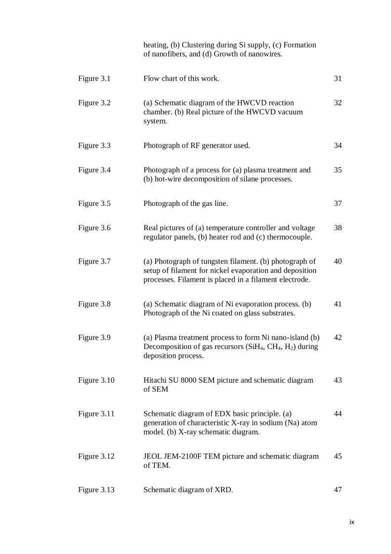
heating, (b) Clustering during Si supply, (c) Formation
of nanofibers, and (d) Growth of nanowires.
Figure 3.1 Flow chart of this work. 31
Figure 3.2 (a) Schematic diagram of the HWCVD reaction
chamber. (b) Real picture of the HWCVD vacuum
system.
32
Figure 3.3 Photograph of RF generator used. 34
Figure 3.4 Photograph of a process for (a) plasma treatment and
(b) hot-wire decomposition of silane processes.
35
Figure 3.5 Photograph of the gas line. 37
Figure 3.6 Real pictures of (a) temperature controller and voltage
regulator panels, (b) heater rod and (c) thermocouple.
38
Figure 3.7 (a) Photograph of tungsten filament. (b) photograph of
setup of filament for nickel evaporation and deposition
processes. Filament is placed in a filament electrode.
40
Figure 3.8 (a) Schematic diagram of Ni evaporation process. (b)
Photograph of the Ni coated on glass substrates.
41
Figure 3.9 (a) Plasma treatment process to form Ni nano-island (b)
Decomposition of gas recursors (SiH4, CH4, H2) during
deposition process.
42
Figure 3.10 Hitachi SU 8000 SEM picture and schematic diagram
of SEM
43
Figure 3.11 Schematic diagram of EDX basic principle. (a)
generation of characteristic X-ray in sodium (Na) atom
model. (b) X-ray schematic diagram.
44
Figure 3.12 JEOL JEM-2100F TEM picture and schematic diagram
of TEM.
45
Figure 3.13 Schematic diagram of XRD. 47

x
Figure 3.14 InVia Raman microscope picture and representation of
Raman scattering from particles.
48
Figure 3.15 KEITHLEY Model 236 source measure unit and
electrode pins picture.
49
Figure 3.16 A schematic diagram of the fabricated Si-based
nanowires heterojunction structure and the electrodes
configuration.
49
Figure 4.1 Variations of substrate temperature, and substrate
surface on Si and glass substrates with filament
temperature.
51
Figure 4.2 FESEM images of the Si-based nanowires synthesis by
HWCVD on silicon at different filament temperatures
(a) 1150C, (b) 1450C, (c) 1650C, (d) 1750C, (e)
1850C, (f) 1950C. Insets show the high
magnification image of the nanowires. (Insets bar is
500 nm).
54
Figure 4.3 FESEM images of the nanowires synthesis by
HWCVD on glass at different filament temperatures.
(a) 1150C, (b) 1450C, (c) 1650C, (d) 1750C, (e)
1850C, (f) 1950C. Insets show the high
magnification image of the nanowires. (Insets bar is
500 nm).
55
Figure 4.4 Variations of nanowire diameter with filament
temperature on silicon and glass substrate.
56
Figure 4.5 Cross-sectional view of FESEM images of the
nanowires prepared by HWCVD at filament
temperature of 1850C. (a) secondary electron (b)
backscattered electron signals (c) backscattered
electron signal collected by a photo-diode
backscattered electron (PDBSE) detector that attached
to the SEM. Insets figures present high magnification
of the FESEM images.
58
Figure 4.6 (a) TEM morphology of the NiSi/Si core-shell NWs
prepared at filament temperature of 1650C. (b) and (d)
HRTEM image of the NWs enlarged from the frame in.
(c) show TEM image of the side wall structures of the
NWs.
61
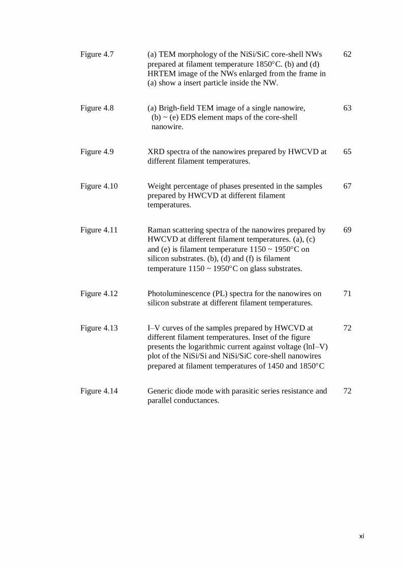
xi
Figure 4.7 (a) TEM morphology of the NiSi/SiC core-shell NWs
prepared at filament temperature 1850C. (b) and (d)
HRTEM image of the NWs enlarged from the frame in
(a) show a insert particle inside the NW.
62
Figure 4.8 (a) Brigh-field TEM image of a single nanowire,
(b) ~ (e) EDS element maps of the core-shell
nanowire.
63
Figure 4.9 XRD spectra of the nanowires prepared by HWCVD at
different filament temperatures.
65
Figure 4.10 Weight percentage of phases presented in the samples
prepared by HWCVD at different filament
temperatures.
67
Figure 4.11 Raman scattering spectra of the nanowires prepared by
HWCVD at different filament temperatures. (a), (c)
and (e) is filament temperature 1150 ~ 1950C on
silicon substrates. (b), (d) and (f) is filament
temperature 1150 ~ 1950C on glass substrates.
69
Figure 4.12 Photoluminescence (PL) spectra for the nanowires on
silicon substrate at different filament temperatures.
71
Figure 4.13 I–V curves of the samples prepared by HWCVD at
different filament temperatures. Inset of the figure
presents the logarithmic current against voltage (lnI–V)
plot of the NiSi/Si and NiSi/SiC core-shell nanowires
prepared at filament temperatures of 1450 and 1850C
72
Figure 4.14 Generic diode mode with parasitic series resistance and
parallel conductances.
72

xii
LIST OF TABLES
Page
Table 1 Nanowire fabrication types and conditions 27
Table 2 Deprosite parameters in this work. 42
Table 3 Experimental values of the parameters obtained from
I–V fittings.
74
xiii
LIST OF SYMBOLS AND ABBREVIATIONS
C Carbon
Ni Nickel
Si Silicon
O2 Oxygen
H2 Hydrogen
SiC Silicon carbide
SiH4 Silane
CH4 Methane
NH4OH Ammonia
HCl Hydrochloric acid
H2O2 Hydrogen peroxide
c-Si Crystal silicon
DI Deionized
sccm Standard cubic centimeters per minute
CVD Chemical vapor deposition
HWCVD Hot-wire chemical vapor deposition
FESEM Field emission scanning electron microscope
EDX Energy dispersive X-ray
HRTEM High resolution transmission electron microscope
STEM Scanning transmission electron microscopy
XRD X-ray diffraction
PL Photoluminescence
PDBSE Photo-diode backscattered electron
HAADF High angle annular dark field
VLS Vapor-liquid-solid
MIG Metal induced growth

xiv
MDG Metal diffusion growth
Ts Surface temperatures for c-Si substrate
Tg Surface temperatures for glass substrate
Tb Temperature on the bottom surface of the substrates
Tf Filament temperature
I-V Current-voltage
1
CHAPTER 1
INTRODUCTION
1.1 Background
Semiconductor nanowires have been extensively studied due to their potential
applications in a wide range of applications (Bae et al., 2010; Rurali, 2010; L. Yu et al.,
2009). The hybrid heterostructures such as core-shell nanowires are expected to
improve the properties of the nanowires such in the case of applications for
high-temperature sensing (Bi et al., 2013), high-performance FET (field effect
transistors) (Xiang et al., 2006) and enhanced hydrogen generation photocatalytic (Hao,
Wang, Tong, Jin, & Guo, 2012).
Design and synthesis of multi-dimensional materials to achieve certain desirable
properties is more complex. These materials are diverse structures that consisted of
metals, semiconductors, carbon, which generally are axially connected to a
heterojunction by two different nanomaterials. One-dimension heterostructure materials
with unique properties and its functionality can be obtained for wide range of
applications in various new fields.
For example, semiconductor-semiconductor p-n junction is formed to produce a
rectified current logic gates (Huang, Duan, Cui, & Lieber, 2002), nano photodetector
(Hayden, Agarwal, & Lieber, 2006) and multifunction light emitting diode (McAlpine,
Ahmad, Wang, & Heath, 2007). Metal-semiconductor-metal heterojunction nanowires
with superior optical and conductivity properties potentially can be used in biosensors
(Penn, He, & Natan, 2003), gene transfer (Salem, Searson, & Leong, 2003) and
2
separation (K. B. Lee, Park, & Mirkin, 2004). It has been reported that metal-metal
heterojunction with different fragments have different functions and features. The
device prepared in this heterojunction has disadvantages in electrical properties.
However, highly mismatched with no dislocation lines can formed in one-dimensional
heterostructure materials. Matthews and Blakeslee et al. recently described the
formation of a two-dimensional heterostructure is not critical thickness for dislocation
(Matthews & Blakeslee, 1974). The model predicted that over the critical radius, nano
heterojunction with instability showed a larger grain. Materials have lattice mismatch,
hardly form a perfect heterojunction without dislocation. Thus, maximum advantage of
the nanowire heterostructure is the size below the critical radius, inappropriate
dislocation does not exist. It is possible to obtain novel, versatile and high-performance
electronic devices.
Depending on the composition, the nano-heterojunction materials can be divided
into follows: (1) Semiconductor-Semiconductor; (2) semiconductor-metal; (3)
metal-metal; (4) carbon-carbon; (5) carbon-metal; (6) carbon-semiconductor
heterojunction, wherein the “carbon” may be carbon nanotubes, amorphous carbon or
diamond. According to different classification of the connections, it include a
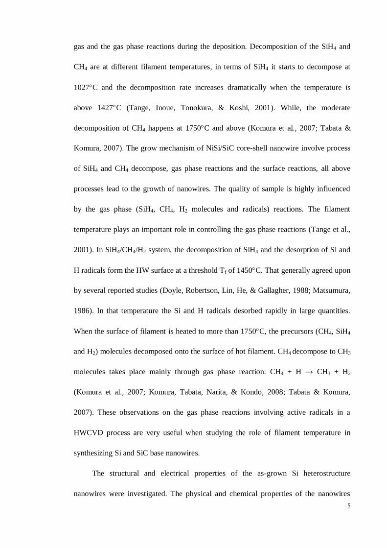
segment-type, a core-shell, cross-type, branch heterojunction type and brushes as shown
in Fig. 1.1 (Mieszawska, Jalilian, Sumanasekera, & Zamborini, 2007). These
heterojunctions play an important role in their properties. There are some synthesis
methods of the material, for example, template synthesis structure and core-shell
heterostructure. This thesis focuses the core-shell heterostructure materials.
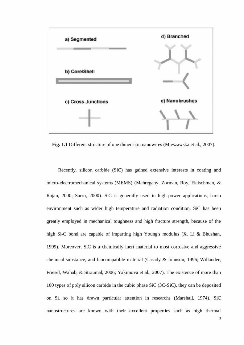
3
Fig. 1.1 Different structure of one dimension nanowires (Mieszawska et al., 2007).
Recently, silicon carbide (SiC) has gained extensive interests in coating and
micro-electromechanical systems (MEMS) (Mehregany, Zorman, Roy, Fleischman, &
Rajan, 2000; Sarro, 2000). SiC is generally used in high-power applications, harsh
environment such as wider high temperature and radiation condition. SiC has been
greatly employed in mechanical toughness and high fracture strength, because of the
high Si-C bond are capable of imparting high Young's modulus (X. Li & Bhushan,
1999). Moreover, SiC is a chemically inert material to most corrosive and aggressive
chemical substance, and biocompatible material (Casady & Johnson, 1996; Willander,
Friesel, Wahab, & Straumal, 2006; Yakimova et al., 2007). The existence of more than
100 types of poly silicon carbide in the cubic phase SiC (3C-SiC), they can be deposited
on Si. so it has drawn particular attention in researchs (Marshall, 1974). SiC
nanostructures are known with their excellent properties such as high thermal
4
conductivity, high mechanical properties, good thermal shock resistance, low thermal
expansion coefficient, as well as its chemical stability and electron affinity, allowing
them working in harsh environments (J. Fan, Wu, & Chu, 2006; Wong, Sheehan, &
Lieber, 1997). By incorporated highly metallic properties of single crystalline NiSi into the
NiSi/SiC core-shell nanowires, that expected to enhance the electrical and optical properties
of this heterostructure material in various applications. The NiSi core electrode could use as
1D electrodes for enhancing the efficiency of electron transfer between current collector
supports and individual electrode materials and ion transport to the electrode (C. J. Kim et
al., 2007; Yue Wu, Xiang, Yang, Lu, & Lieber, 2004). Moreover, this
metallic/semiconductor heterostructures probably could enhance the carry mobilities which
would significantly improve the performance of existing nanowires-based devices (Lauhon,
Gudiksen, Wang, & Lieber, 2002).
Recently, extensive works have been carried up to investigate the properties of
Si-based heterostructures. they using various deposition techniques include chemical
vapor deposition (CVD), hot-wire chemical vapor deposition (HWCVD), lithography
and laser ablation (Bandaru & Pichanusakorn, 2010; H. J. Fan, Werner, & Zacharias,
2006; Rao, Deepak, Gundiah, & Govindaraj, 2003; Suzuki, Araki, Tosa, & Noda, 2007).
In this work, the Si-based heterostructure nanowires have been grown by HWCVD at
different filament temperatures. HWCVD is a preferable technique for the fabrication of
Si-based nanowires with lower cost production and large-area deposition. Moreover,
HWCVD also capable in generating high density of grow precursors (SiH3 and CH3) by
using high temperature tungsten filament as a catalyst. In the HWCVD, the filament
temperature is playing an important role in controlling the decomposition of the source
5
gas and the gas phase reactions during the deposition. Decomposition of the SiH4 and
CH4 are at different filament temperatures, in terms of SiH4 it starts to decompose at
1027C and the decomposition rate increases dramatically when the temperature is
above 1427C (Tange, Inoue, Tonokura, & Koshi, 2001). While, the moderate
decomposition of CH4 happens at 1750C and above (Komura et al., 2007; Tabata &
Komura, 2007). The grow mechanism of NiSi/SiC core-shell nanowire involve process
of SiH4 and CH4 decompose, gas phase reactions and the surface reactions, all above
processes lead to the growth of nanowires. The quality of sample is highly influenced
by the gas phase (SiH4, CH4, H2 molecules and radicals) reactions. The filament
temperature plays an important role in controlling the gas phase reactions (Tange et al.,
2001). In SiH4/CH4/H2 system, the decomposition of SiH4 and the desorption of Si and
H radicals form the HW surface at a threshold Tf of 1450C. That generally agreed upon
by several reported studies (Doyle, Robertson, Lin, He, & Gallagher, 1988; Matsumura,
1986). In that temperature the Si and H radicals desorbed rapidly in large quantities.
When the surface of filament is heated to more than 1750C, the precursors (CH4, SiH4
and H2) molecules decomposed onto the surface of hot filament. CH4 decompose to CH3
molecules takes place mainly through gas phase reaction: CH4 + H → CH3 + H2
(Komura et al., 2007; Komura, Tabata, Narita, & Kondo, 2008; Tabata & Komura,
2007). These observations on the gas phase reactions involving active radicals in a
HWCVD process are very useful when studying the role of filament temperature in
synthesizing Si and SiC base nanowires.
The structural and electrical properties of the as-grown Si heterostructure
nanowires were investigated. The physical and chemical properties of the nanowires
6
such as morphological, microstructure and compositions were investigated by field
emission scanning electron microscopy (FESEM), high resolution transmission electron
microscopy (HRTEM), X-ray diffraction (XRD) and micro-Raman scattering
spectroscopy. Current-voltage (I-V) characteristics were used to analyze electrical
properties of the nanowires.
1.2 Problem statement
Generally, the single-phased intrinsic materials generally have low conductivity,
week mechanical stability and associated side reactions due to their unprotected
surfaces, which make them unsuitable for various device applications (Fu et al., 2006;
Liu, Li, Ma, & Cheng, 2010). These disadvantages has made the nanowires lack of
interest in applications energy conversion and storage. Therefore, hybrid core–shell
nanowires have become new approach for these applications. The incorporation of
highly metallic properties of single-crystalline NiSi nanowires as core electrodes into
the NiSi/SiC core-shell is expected to enhance their electrical and optical properties.
The NiSi core electrodes could be used as 1D electrodes for enhancing the efficiency of
electron transfer between the current collector supports and individual electrode
materials as well as of ion transport to the electrode (Cohen-Karni et al., 2012; Yue Wu,
Xiang, et al., 2004). Moreover, this metallic/semiconductor heterostructure could
possibly enhance the carrier mobility which would significantly improve the
performance of the existing nanowire-based devices.
7
1.3 Motivation of this work
Si-based nanostructures such as nanowires, nanorods and nanotubes have attracted
more and more attention due to their applications in nanoscale devices.
One-dimensional materials are excellent in electrical, optical and magnetic properties.
Hence, there great potential to be used in nanoelectronics, photonics, laser plasma,
medical diagnostics, drug delivery and chemical sensors. SiC is a wide band gap
semiconductor used for high temperature, high power applications and radiation–hard
environment. By incorporated highly metallic properties of single crystalline NiSi
nanowires as a core electrode into the NiSi/SiC core-shell nanowires is expected to enhance
the electrical and optical properties of this heterostructures material in various applications.
The NiSi core is believed to be able in boost the efficiency of electron transfer between
current collector supports and individual electrode materials, as well as that of ion transport
to the electrode. Moreover, this metallic/semiconductor heterostructure probably could
enhance the carrier mobilities, which would significantly improve the performance of
existing nanowires-based devices.
1.4 Objectives
The objectives of this research are:
1) To investigate the role of filament temperature on the growth of Ni-catalyzed
Si-based core-shell nanowires by HWCVD on c-Si and glass substrates,
2) To analyze the structural, optical and electrical properties of the nanowires,
8
1.5 Thesis overview
This thesis is organized mainly into five chapters. The first chapter describes the
introduction of one-dimensional core-shell nanowires included the objectives,
motivation of the work and also an outline of the report. Chapter 2 presents the
literature review of this work. The description of the advantages of nickel silicide,
silicon carbide and heterostructure of nanowires also include in this chapter. Also
discuss the importance of using HWCVD system. Chapter 3 details description on the
research methodology include the experimental setup, material used and
characterization techniques of this work. Chapter 4 present the results and discussion of
this work. Chapter 5 is summary and conclusion of the work done in this work.
9
CHAPTER 2
LITERATURE REVIEW
2.1 Nanomaterials and Nanotechnology
When the size of particles is 0.1 micron (100 nm) or less, the unit is generally
nano. The physical and chemical properties are significantly different from normal size.
Nanotechnology studies the characteristics and interactions in the range of 0.1 to 100
nm. Nanotechnology research indicates that macro to micro of an object is made, a large
size to a small size, and also the nano-micron level of development. Numerous studies
have showed a number of specific physical, chemical and biological properties
exhibited differently when the size of the material is at the nanometer level, from the
material at the macroscopic state that reflect the nature of the special nature of these
nanoscale that emerging into high technology industries (Kalantar-zadeh & Fry, 2007).
Due to nanoscale dimensions, nanomaterials exhibit small size effect, quantum
tunneling effect, Coulomb blockade effects and surface effects due to the fluctuations
between the electrons and atomic interactions of nanomaterials. Nanomaterials possess
properties that many of the materials do not have especially in the physical, chemical
and biological properties. Due to surface effects, as in the reduction in particle size of
nano-materials, a sharp increase in specific surface area of the material, the number of
atoms in the proportion of the surface of the bulk atoms is also greatly increased, while
the surface energy and the surface tension increases, which causes nanomaterials change
in nature. As the particle diameter becomes smaller, the specific surface area will be
significantly increased, the number of surface atoms is also increasing rapidly. For
10
instance, a particle size of 10 nm with the specific surface area of 90 m2/g; when the
particle diameter is 5 nm, the specific surface area of 180 m2/g, the number of surface
atoms to account for 50 %, particle size down to 2 nm, specific surface area soared to
450 m2/g, the number of surface atoms to 80 %. The surface atomic ratio of the total
number of nanomaterials atoms will increase rapidly when the size of nano-material is
reduced to 10 nm or less. The surface on these atoms nanomaterials have high activity,
very unstable, and very easy to combine with other atoms. The metal nanoparticles in
the air easily burn the inorganic nanoparticles when it is exposed to the gas in the air in
which it will absorb and react. This feature has been used to construct miniature sensors
and detectors. As the size of the amount gradually reaching the nanoscale under certain
critical conditions, some changes can cause to the nature. The effects when the
coherence of length of nanomaterials size and light wavelength, the de Broglie
wavelength or superconducting state or transmitted physical characteristics and depth
dimensions comparable or smaller are that the periodic boundary conditions of the
crystal material will be destroyed, the electronic transport behaviour received
limitations, the electron mean free path is shortened, and the coherence of electrons
localized enhancements, resulting nanomaterials there are special sound, light,
electricity, magnetic, thermal, mechanical and other properties (Wan et al., 2009; Xia et
al., 2003; R. Yan, Gargas, & Yang, 2009).
2.2 One-dimensional NiSi and SiC nanowire
Silicide is silicon compound with a metal as electropositive component (J. Kim &
Anderson, 2005). It can reduce the resistivity of local-interconnect metallization and
11
gate and is commonly used in silicon based microelectronics. CoSi2 and TiSi2 are some
popular silicide candidates (Han, Liu, & Zhao, 2015), however there are some
limitations. For example TiSi2 line width and the sheet resistance of the display depends
C49 phase. Therefore it is difficult to transit to a low resistivity C54 phase. CoSi2 film
consumes more Si compared TiSi2 (Colgan, Gambino, & Cunningham, 1996).
Presented in nickel siliciden (NiSi), some of the advantages of low resistivity, lower Si
consumption and the formation of a relatively low temperature, and therefore it is a
promising material to replace those silicide material (G. B. Kim et al., 2003). NiSi has
been used as an ideal source for electrical contact materials and recently the NiSi
provided the drain and gate complementary metal oxide silicon devices. In addition,
they also exhibit superior performance to reduce the proportion of (Lavoie, d’Heurle,
Detavernier, & Cabral, 2003).
There has been abundance reported on NiSi nanowire growths. Metal-induced
growth (MIG) method is a unique nanowire growth mechanism that the NiSi nanowire
follows (J. Kim & Anderson, 2005). Highly straight NiSi nanowires grown by a
sputtering method at 575C followed a solid-phase reaction of Ni and Si (J. Kim, 2010).
Low temperature process is preferably applied as a nanowire interconnected with the
structure of the manufactured nanoscale little or no damage. MIG has advantage among
a growing number of epitaxial Si film, which uses solid phase crystallization and solid
phase epitaxy mechanisms. The behavior of the deposited metal catalyst film which act
as a seed layer, the sputtering silicon interact to form a silicide layer on top of it grown
Si film. Nickel and cobalt are commonly used as metal catalyst in MIG method. Si
epitaxial film growth and to exhibit the spontaneous formation of a good ohmic contact
12
layer, a thin film or small CoSi2 and NiSi2 lattice mismatch provides an excellent
precursor layer. MIG method is rapid crystallization of silicon at low temperature and
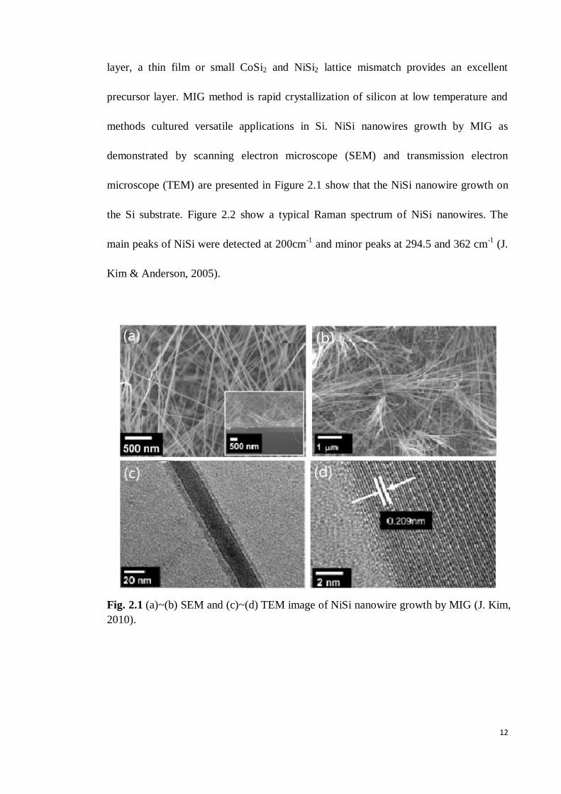
methods cultured versatile applications in Si. NiSi nanowires growth by MIG as
demonstrated by scanning electron microscope (SEM) and transmission electron
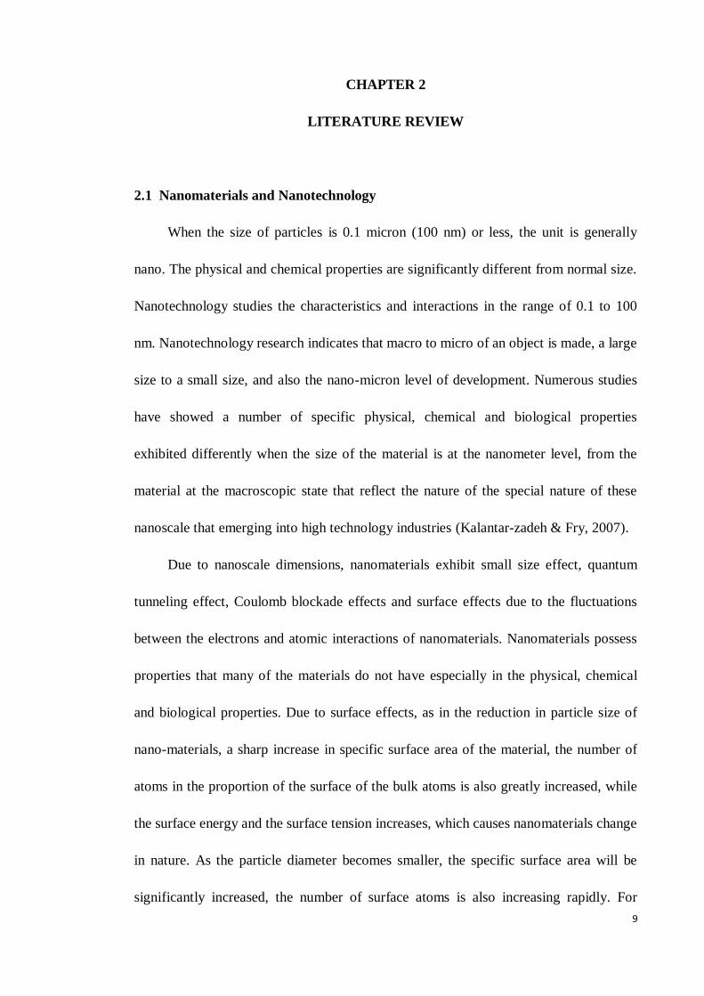
microscope (TEM) are presented in Figure 2.1 show that the NiSi nanowire growth on
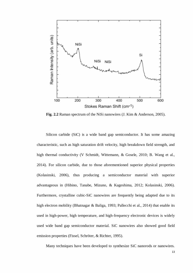
the Si substrate. Figure 2.2 show a typical Raman spectrum of NiSi nanowires. The
main peaks of NiSi were detected at 200cm-1
and minor peaks at 294.5 and 362 cm-1
(J.
Kim & Anderson, 2005).
Fig. 2.1 (a)~(b) SEM and (c)~(d) TEM image of NiSi nanowire growth by MIG (J. Kim,
2010).
13
Fig. 2.2 Raman spectrum of the NiSi nanowires (J. Kim & Anderson, 2005).
Silicon carbide (SiC) is a wide band gap semiconductor. It has some amazing
characteristic, such as high saturation drift velocity, high breakdown field strength, and
high thermal conductivity (V Schmidt, Wittemann, & Gosele, 2010; B. Wang et al.,
2014). For silicon carbide, due to those aforementioned superior physical properties
(Kolasinski, 2006), thus producing a semiconductor material with superior
advantageous in (Hibino, Tanabe, Mizuno, & Kageshima, 2012; Kolasinski, 2006).
Furthermore, crystalline cubic-SiC nanowires are frequently being adapted due to its
high electron mobility (Bhatnagar & Baliga, 1993; Pallecchi et al., 2014) that enable its
used in high-power, high temperature, and high-frequency electronic devices is widely
used wide band gap semiconductor material. SiC nanowires also showed good field
emission properties (Fissel, Schröter, & Richter, 1995).
Many techniques have been developed to synthesize SiC nanorods or nanowires.
14
Dai et al. (Dai, Wong, Lu, Fan, & Lieber, 1995) were the first to synthesis SiC nanorods
and succeeded in 1995 through the reaction of carbon nanotubes with SiO or Si + I2.
H-SiC nanorods was synthesis by Meng et al. (Meng, 1998) using carbothermal
reduction reaction, and SiC nanowires was fabricated using the hot filament CVD
method by Zhou et al. (Zhou et al., 1999). Li et al. (Y. Li et al., 2001) synthesized SiC
nanowires by using silicon carbide rod as the anode arc discharge lately. There are some
difficulties during the course of the reaction, to synthesize the SiC nanorods and
nanowires on a Si substrate directly, since these methods use a variety of reactants, and
the reaction requires high temperatures (typically greater than 1200C). SiC nanowires
were synthesized at low temperatures with high pressure by some groups (Lu et al.,
1999). There are also reports on synthesis of SiC nanowires using metal as a catalyst
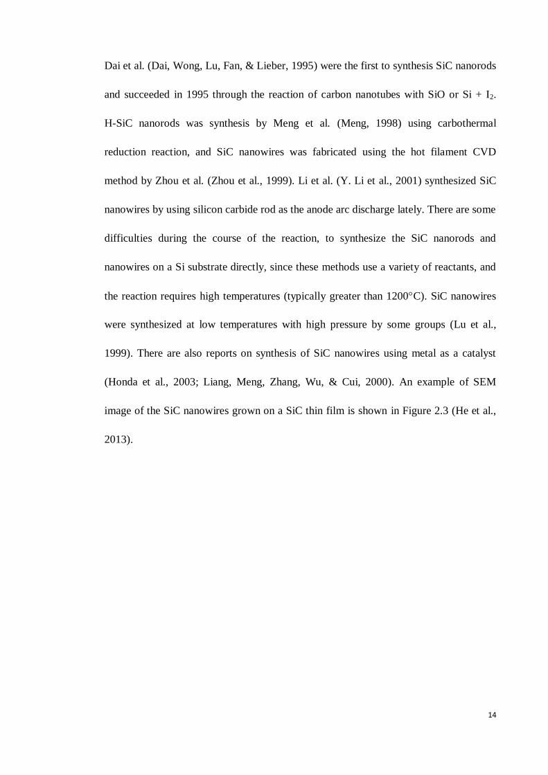
(Honda et al., 2003; Liang, Meng, Zhang, Wu, & Cui, 2000). An example of SEM
image of the SiC nanowires grown on a SiC thin film is shown in Figure 2.3 (He et al.,
2013).
15
Fig. 2.3 Typical SEM images of SiC nanowires (He et al., 2013).
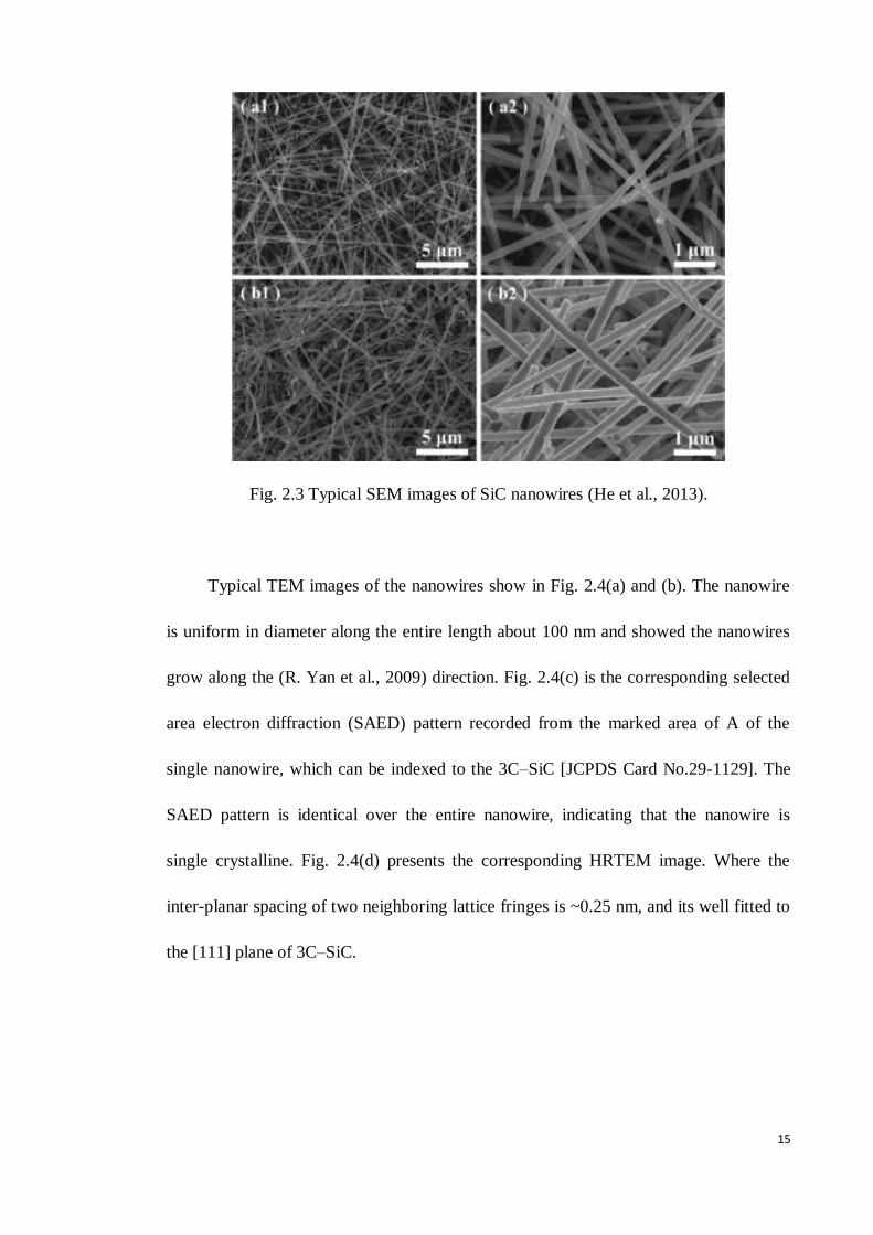
Typical TEM images of the nanowires show in Fig. 2.4(a) and (b). The nanowire
is uniform in diameter along the entire length about 100 nm and showed the nanowires
grow along the (R. Yan et al., 2009) direction. Fig. 2.4(c) is the corresponding selected
area electron diffraction (SAED) pattern recorded from the marked area of A of the
single nanowire, which can be indexed to the 3C–SiC [JCPDS Card No.29-1129]. The
SAED pattern is identical over the entire nanowire, indicating that the nanowire is
single crystalline. Fig. 2.4(d) presents the corresponding HRTEM image. Where the
inter-planar spacing of two neighboring lattice fringes is ~0.25 nm, and its well fitted to
the [111] plane of 3C–SiC.
16
Fig. 2.4 (a)~(b) Typical TEM images of a single SiC nanowire. (c)~(d) corresponding
SAED pattern and HRTEM image of the SiC nanowire (He et al., 2013).
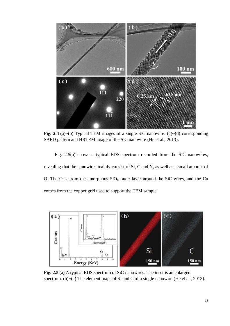
Fig. 2.5(a) shows a typical EDS spectrum recorded from the SiC nanowires,
revealing that the nanowires mainly consist of Si, C and N, as well as a small amount of
O. The O is from the amorphous SiOx outer layer around the SiC wires, and the Cu
comes from the copper grid used to support the TEM sample.
Fig. 2.5 (a) A typical EDS spectrum of SiC nanowires. The inset is an enlarged
spectrum. (b)~(c) The element maps of Si and C of a single nanowire (He et al., 2013).
17
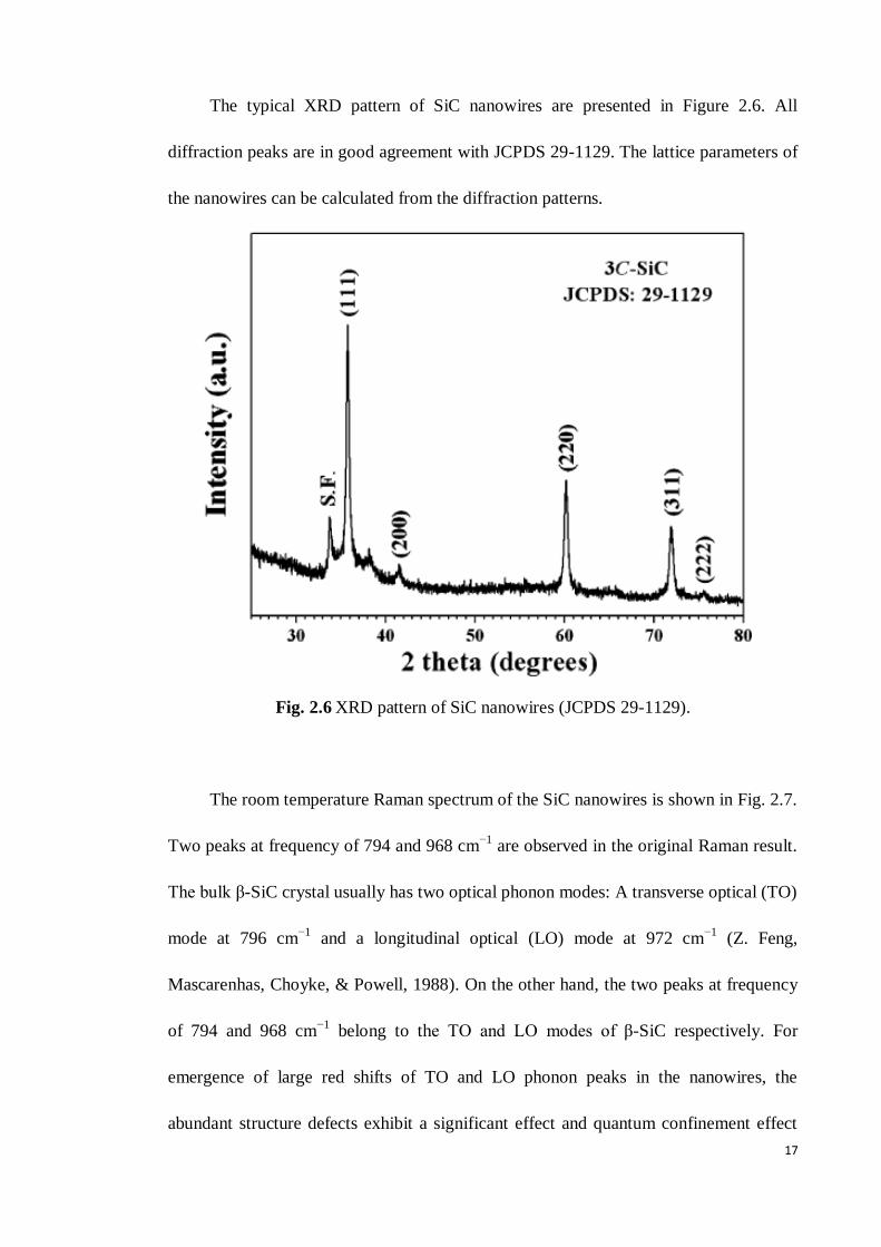
The typical XRD pattern of SiC nanowires are presented in Figure 2.6. All
diffraction peaks are in good agreement with JCPDS 29-1129. The lattice parameters of
the nanowires can be calculated from the diffraction patterns.
Fig. 2.6 XRD pattern of SiC nanowires (JCPDS 29-1129).
The room temperature Raman spectrum of the SiC nanowires is shown in Fig. 2.7.
Two peaks at frequency of 794 and 968 cm−1
are observed in the original Raman result.
The bulk β-SiC crystal usually has two optical phonon modes: A transverse optical (TO)
mode at 796 cm−1
and a longitudinal optical (LO) mode at 972 cm−1
(Z. Feng,
Mascarenhas, Choyke, & Powell, 1988). On the other hand, the two peaks at frequency
of 794 and 968 cm−1
belong to the TO and LO modes of β-SiC respectively. For
emergence of large red shifts of TO and LO phonon peaks in the nanowires, the
abundant structure defects exhibit a significant effect and quantum confinement effect
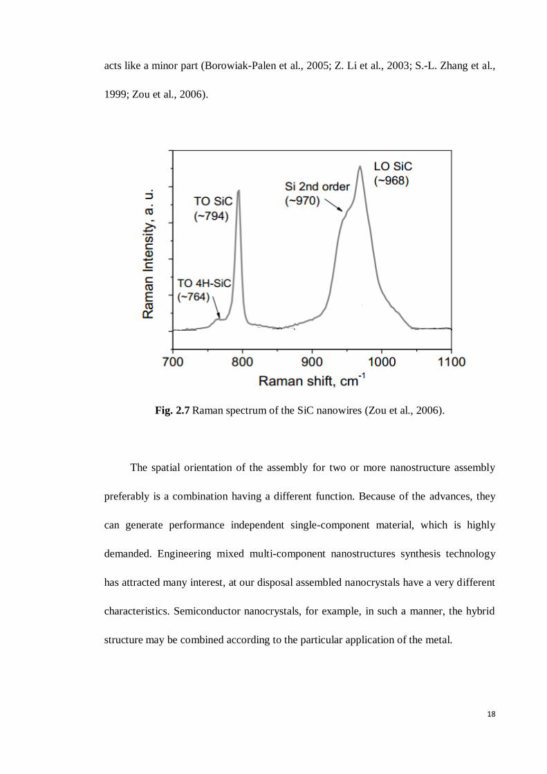
18
acts like a minor part (Borowiak-Palen et al., 2005; Z. Li et al., 2003; S.-L. Zhang et al.,
1999; Zou et al., 2006).
Fig. 2.7 Raman spectrum of the SiC nanowires (Zou et al., 2006).
The spatial orientation of the assembly for two or more nanostructure assembly
preferably is a combination having a different function. Because of the advances, they
can generate performance independent single-component material, which is highly
demanded. Engineering mixed multi-component nanostructures synthesis technology
has attracted many interest, at our disposal assembled nanocrystals have a very different
characteristics. Semiconductor nanocrystals, for example, in such a manner, the hybrid
structure may be combined according to the particular application of the metal.
19
2.3 Nanowire diode
There has been steady progress in demonstrating electrical components made of
nanowires, such as field effect transistors, electron field emitters, switches, sensors, etc.
The surface of the nanostructures has crucial role in determining the electrical and
optoelectronic properties of nanodevices. As the surface-to-volume ratio is very high,
the surface states also play a key role on optical absorption, gas sensing, luminescence
and other properties. Thus, nanoscale electronic devices have the potential to achieve
higher sensitivity and faster response than bulk material(Das, Myoung, & Kar, 2011).
Nanodevice units made from those one-dimensional nanostructures (single
nanostructures as well as bunch of nanostructures) have attracted substantial research
interests because they provide a unique platform for fundamental investigations. In
addition, they can also serve as the building blocks for more complicated nano-systems
and microsystems.
2.4 Hot-wire Chemical Vapor Deposition (HWCVD)
Low pressure chemical vapor deposition (LPCVD) method has widely been used
to develop Si/SiC core-shell nanowires, (Choi, Yao, Cui, & Cho, 2011). However, this
technique has some disadvantages that include lower deposition rates and it also needed
high temperature usually above 600C for the process. Pressure and temperature are two
variables that control the deposition rate (Curley, McCormack, & Phipps). Other
techniques such as hot-wire chemical vapor deposition (HWCVD) also can be used in
producing Si/SiC core-shell nanowires.
HWCVD is an elegant low pressure deposition technique that base on thermal
20
decomposition of precursor gases at the surface of resistively heated filament (usually
Tungsten) to form radicals. These radicals adsorbed on the heated substrate (J. C. Lee et
al., 2002).
Due to the lower production cost and large scale production capability, for the
monent HWCVD has become a preferred-technique for the fabrication of Si/SiC
core-shell nanowires. As a result making this method is getting attractive respecrally for
industrial applications. It is also proven that this technique enhance the growth rate of Si
nanowires besides having the advantages of low-temperature growth processess.
Moreover, HWCVD is comparatively a better technique for the growth of Si/SiC
core-shell nanowires since it provides an ion-free deposition by catalytical
decomposition of the source gas using a catalyzer usually tungsten.
HWCVD was proposed in 1979 by Wiesmann (Wiesmann, Ghosh, McMahon, &
Strongin, 1979) in the preparation of highly hydrogenated amorphous silicon (a-Si:H)
film, but the electrical properties of hydrogenated amorphous silicon was inferior to the
film prepared by plasma-enhanced chemical vapor deposition (PECVD). Due to this
reason, this technique has been neglected until after 1985 Matsumura et al prepared
excellent fluorinated amorphous silicon by the use of this technique (Matsumura &
Tachibana, 1985). Because they believe the deposition process, the hot tungsten
filament act as a catalyst, then this process is called catalytic chemical vapor deposition
(catalytic CVD). Doyel, who after three years under similar conditions to prepare a
good quality hydrogenated amorphous silicon, they call the evaporation surface
decomposition (evaporative surface decomposition), because they think the hot-wire
decompose air source into primitives that was used in the deposition (Doyle et al., 1988).
21
1991 Mhana prepared device-level quality by hot-wire having, the hydrogen content
only 1 % of a-Si: H and compare the different with PECVD and HWCVD, because
suspect the catalytic reaction with hydrogen and hot-wire, he re-name this process hot
filament assisted chemical vapor deposition, which sparked a passion to HWCVD study
(Mahan, Carapella, Nelson, Crandall, & Balberg, 1991).
Silane pyrolysis has been used as silicon source for numerous of decades.
Although the deposition surface temperature was low than the filament temperature (Tf),
but it is a surface pyrolysis process (R Robertson, Hils, & Gallagher, 1984; Robert
Robertson & Gallagher, 1986). Before prepared a-Si:H, HWCVD is also used to prepare
diamond by pyrolysis mixture CH4/H2. However, in the preparation of the diamond the
pressure is far low than preparation of the silicon based device, which makes the kind of
filament and atmosphere around the filament is not important to the growth diamond. In
contrast, silicon-based nano-wire is prepared mainly under low pressure, there are one
or two times reactive before deposition, thus making a kind of excitation from the
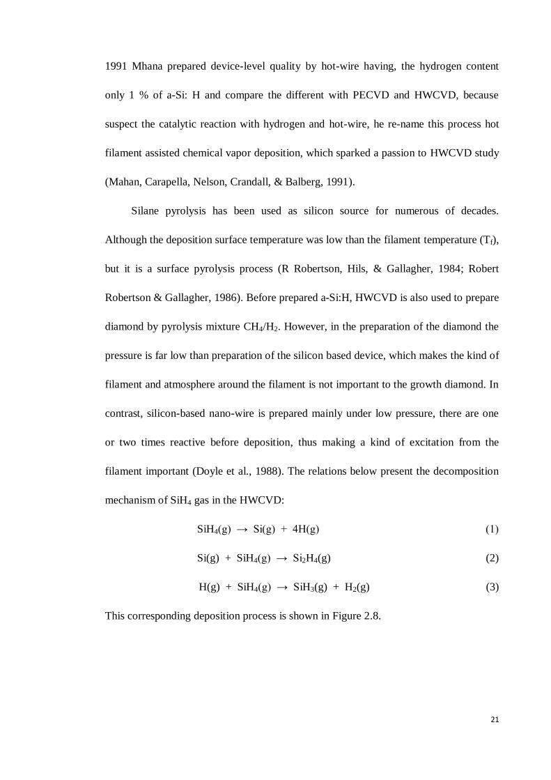
filament important (Doyle et al., 1988). The relations below present the decomposition
mechanism of SiH4 gas in the HWCVD:
SiH4(g) → Si(g) + 4H(g) (1)
Si(g) + SiH4(g) → Si2H4(g) (2)
H(g) + SiH4(g) → SiH3(g) + H2(g) (3)
This corresponding deposition process is shown in Figure 2.8.
22
Fig. 2.8 SiH4 deposit process of hot-wire chemical vapor deposition (Doyle et al.,
1988).
Doyle team studied SiH4 decomposition efficiency tungsten surface and the
relationship with kinds of primitive and hot filament temperature (Matsumura, 1986) It
was found that at lower pressure, when. Tf > 1800C, the probability of reaction of the
silane is relatively high, then the primitives of thermal decomposition silane mainly four
H atoms and one Si atoms. At higher temperatures, H atoms can be more quickly escape
from the hot filament surface. For this case, the high energy of hot-wire, there are high
probability of reaction with silane and tungsten surface dangling bond, and decomposed
into Si and H atoms. The decrease of the hot filament temperature below 1800C,
tungsten surface dangling bonds are occupied by H, a silane and tungsten surface
dangling bonds reduce the probability of reaction, so that the silane can not be
combined with the tungsten surface (Matsumura, 1986). The energy of H decomposition
is low, so just H primitive come out when Tf further reduced to 1500C, the release of
Si primitives becomes negligible, almost all of the silane are decomposed Si and W are
23
a bond and W into the lattice structure of the compound becomes. Surprisingly, when
the tungsten wire temperature below 1300C, still H atoms are released.
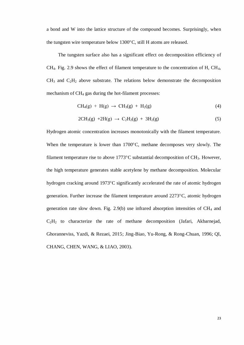
The tungsten surface also has a significant effect on decomposition efficiency of
CH4. Fig. 2.9 shows the effect of filament temperature to the concentration of H, CH4,
CH3 and C2H2 above substrate. The relations below demonstrate the decomposition
mechanism of CH4 gas during the hot-filament processes:
CH4(g) + H(g) → CH3(g) + H2(g) (4)
2CH3(g) +2H(g) → C2H2(g) + 3H2(g) (5)
Hydrogen atomic concentration increases monotonically with the filament temperature.
When the temperature is lower than 1700C, methane decomposes very slowly. The
filament temperature rise to above 1773C substantial decomposition of CH3. However,
the high temperature generates stable acetylene by methane decomposition. Molecular
hydrogen cracking around 1973C significantly accelerated the rate of atomic hydrogen
generation. Further increase the filament temperature around 2273C, atomic hydrogen
generation rate slow down. Fig. 2.9(b) use infrared absorption intensities of CH4 and
C2H2 to characterize the rate of methane decomposition (Jafari, Akbarnejad,
Ghoranneviss, Yazdi, & Rezaei, 2015; Jing-Biao, Yu-Rong, & Rong-Chuan, 1996; QI,
CHANG, CHEN, WANG, & LIAO, 2003).
24
Fig. 2.9 (a) Mode fraction and (b) infrared absorption intensities of C2H2 and CH4 as a
function of filament temperature (Jing-Biao et al., 1996; QI et al., 2003).
2.5 Nanowire grow mechanism
There are several growth mechanism of nanowires were reported, such as
gas-liquid-solid (VLS), solid-liquid-solid (SLS), and solid-solid (SS) type.
The VLS model that was fristly proposed by Wagner and Treuting, still greatly
adopted until today in growing nanowires (Edwards & Happel Jr, 1962; Wagner & Ellis,
1964). As for absorbing liquid catalyst gas-phase reactants (Morales & Lieber, 1998)
strongly favored spots. the number of possible catalyst materials are quite large (Table
1). Although the quality of the wires obtained as well as the required growth conditions
differ strongly, there are also similarities in the behavior of the different catalysts. I will
adopt the classification scheme similarly introduced by Bootsma et al. (Yiying Wu &
Yang, 2001). The catalyst materials are classified into three different categories: typeA,
type-B, and type-C, as shown in Figure 2.10(a). Type-A catalysts are the Au-like metals.
Their phase diagram is of the simple eutectic type; that is, it is dominated by a single
eutectic point. Type-B catalysts are the low Si solubility metals. Their phase diagrams
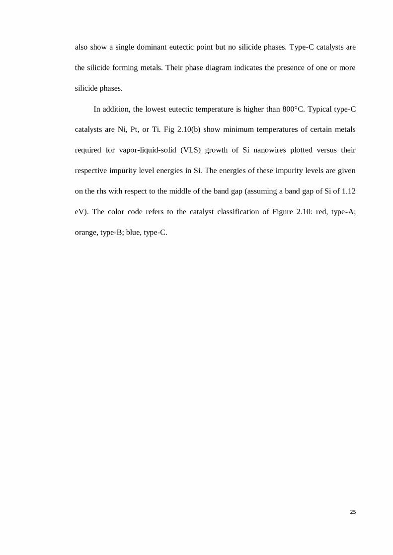
25
also show a single dominant eutectic point but no silicide phases. Type-C catalysts are
the silicide forming metals. Their phase diagram indicates the presence of one or more
silicide phases.
In addition, the lowest eutectic temperature is higher than 800C. Typical type-C
catalysts are Ni, Pt, or Ti. Fig 2.10(b) show minimum temperatures of certain metals
required for vapor-liquid-solid (VLS) growth of Si nanowires plotted versus their
respective impurity level energies in Si. The energies of these impurity levels are given
on the rhs with respect to the middle of the band gap (assuming a band gap of Si of 1.12
eV). The color code refers to the catalyst classification of Figure 2.10: red, type-A;
orange, type-B; blue, type-C.
26
Fig. 2.10 (a) Periodic table with potential catalyst metals classified according to their phase diagram. (b) Minimum temperatures of certain
metals required for vapor-liquid-solid (VLS) growth of Si nanowires (V. Schmidt, Wittemann, & Gösele, 2010).
27
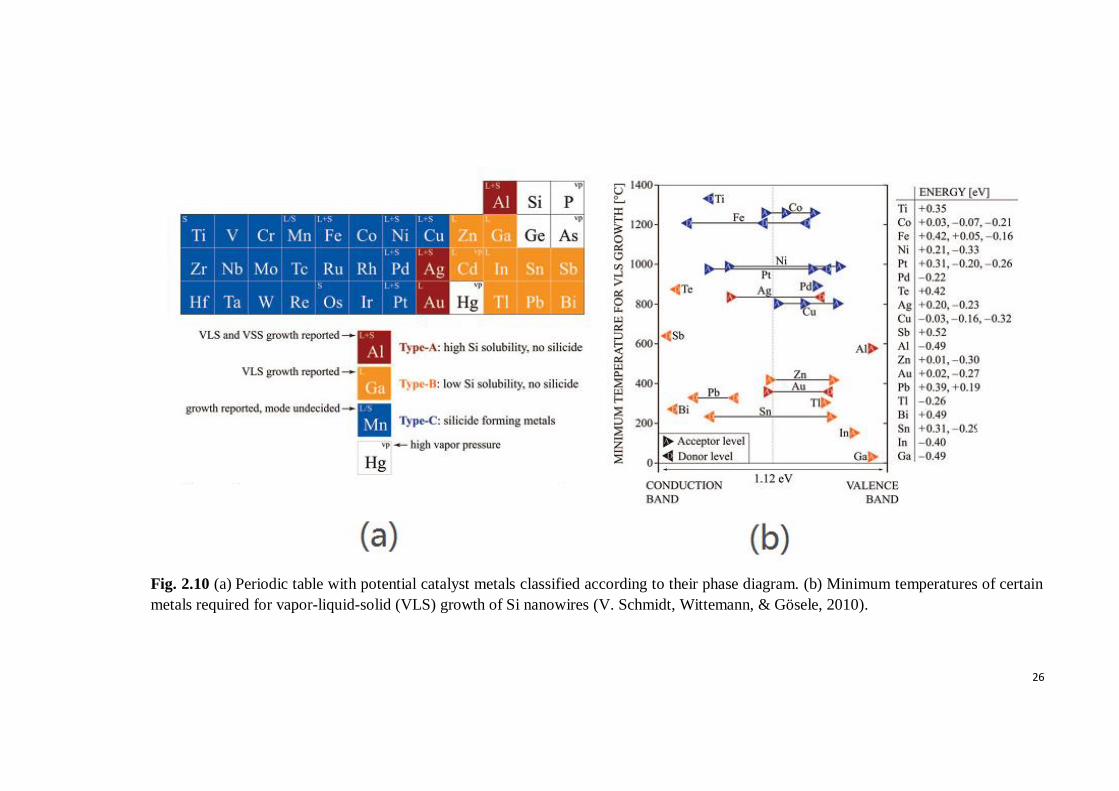
TABLE 1. Nanowire fabrication types and conditions
Growth type Catalyst Gas type Si source Temperature (C) Reference(s)
VLS Au Yes 300–600
(Cui, Lauhon, Gudiksen, Wang, & Lieber, 2001; Westwater,
Gosain, Tomiya, Usui, & Ruda, 1997; Yue Wu, Cui, et al., 2004;
Zeng et al., 2003)
VLS Fe No 1150-1200
(S. Feng, Yu, Zhang, Bai, & Ding, 2000; N. Wang et al., 1999; D.
Yu et al., 1998; H. Zhang et al., 1998)
SLS Ni No 950 (Xihong Chen, Xing, Xu, Xiang, & Yu, 2003; H. Yan et al., 2000)
SS Ni Yes 1050 (K.-H. Lee et al., 2004)
MIG Ni No 575 (J. Kim & Anderson, 2005)
MDG Ni Yes 320–420 (J. Kim & Anderson, 2005)
28
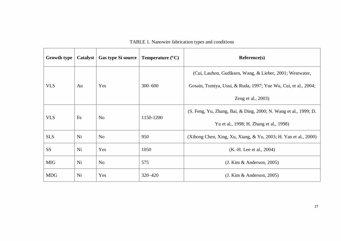
Numerous studies had reported nanowire can be grown in the temperature range
of 320-600C by using gas type silicon source such as silicon tetrachloride or SiH4 with
the presence of Au as catalyst (Cui et al., 2001; Westwater et al., 1997; Yue Wu, Cui, et
al., 2004; Zeng et al., 2003). Fig. 2.11 shows schematic diagram of VLS growth
mechanism. At frist the vapor phases of Si-H would react with the used catalysts of Au,
leading to the formation of molten Au alloy catalytic droplets (schematically shown as
step I in Fig. 2.11). With the increase of the temperature, the vapor species would
dissolve in the formed catalyst liquid droplets, thus leading to the nucleation of Si
nanowires (schematically shown as step II in Fig. 2.11). At the beginning of the growth
of Si crystals, the small size of the nuclei, compared to the large catalyst droplet, would
result in a large contact angle between the nuclei and catalytic droplet, which generates
an outward force (F) on the nanostructure (shown as the marked area of V in Fig. 2.11).
Fig. 2.11 Schematic illustration for the growth of nanowires with on the VLS
mechanism (Cui et al., 2001).
Otherwise, the high temperature near or above 1000C is necessary to liquefy the
catalyst and the Si (S. Feng et al., 2000; N. Wang et al., 1999; D. Yu et al., 1998; H.
Zhang et al., 1998). Recently, SLS synthesis using metal catalyst coated Si prevents
29
direct evaporation of Si atoms, but the results in the formation of droplets of silicon and
metal, even under high temperature 900-950C (Xihong Chen et al., 2003; H. Yan et al.,
2000). It is also claimed that SS synthesized in 1050C by simple heat treatment in the
growth of nanowires CH4: H2 gas mixture. In this mechanism, at the tip of the nanowire,
the SLS mechanism has been observed different metal particles (K.-H. Lee et al.,
2004).
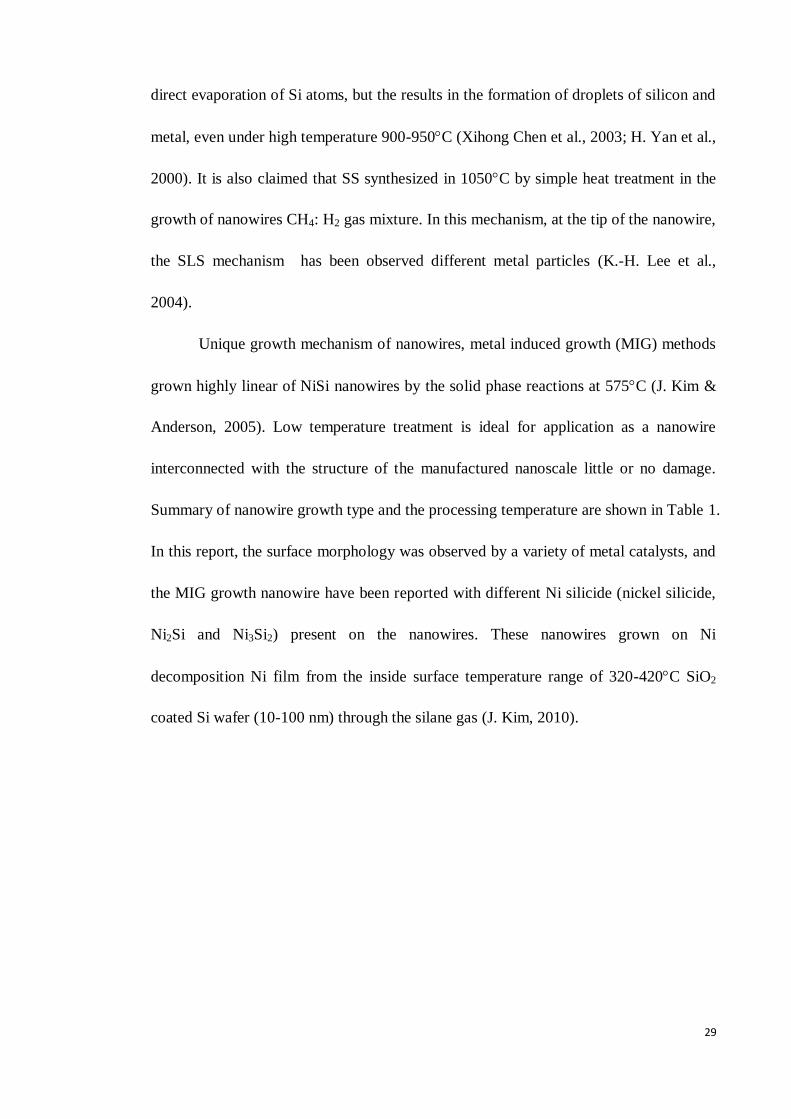
Unique growth mechanism of nanowires, metal induced growth (MIG) methods
grown highly linear of NiSi nanowires by the solid phase reactions at 575C (J. Kim &
Anderson, 2005). Low temperature treatment is ideal for application as a nanowire
interconnected with the structure of the manufactured nanoscale little or no damage.
Summary of nanowire growth type and the processing temperature are shown in Table 1.
In this report, the surface morphology was observed by a variety of metal catalysts, and
the MIG growth nanowire have been reported with different Ni silicide (nickel silicide,
Ni2Si and Ni3Si2) present on the nanowires. These nanowires grown on Ni
decomposition Ni film from the inside surface temperature range of 320-420C SiO2
coated Si wafer (10-100 nm) through the silane gas (J. Kim, 2010).
30
Fig. 2.12 Schematic diagram and SEM image of MIG nanowire growth. (a) Groove and
agglomeration of Ni layer by heating, (b) Clustering during Si supply, (c) Formation of
nanofibers, and (d) Growth of nanowires (J. Kim & Anderson, 2005).
31
CHAPTER 3
METHODOLOGY
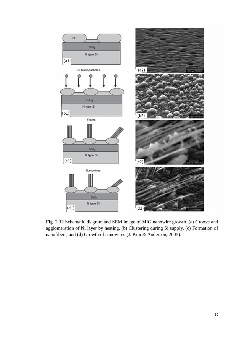
3.1 Introduction
This chapter is organized mainly into 3 sections. The first section describes the
HWCVD system that used for synthesis of the nanowires. Section 3.2 explains the
experimental techniques for substrate cleaning and deposition procedures. The last
section discusses the characterization technique used in this work.
Fig. 3.1 Flow chart of this work.
3.2 Hot-Wire Chemical Vapor Deposition
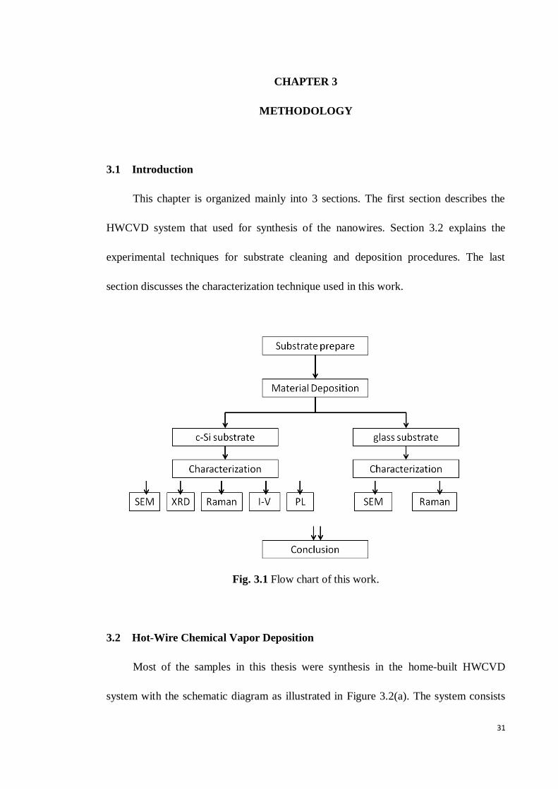
Most of the samples in this thesis were synthesis in the home-built HWCVD
system with the schematic diagram as illustrated in Figure 3.2(a). The system consists
32
of six parts; the vacuum chamber, plasma generator, hot-wire power supply, vacuum
pump, valve, gas line management and substrate heating elements.
View portHot filament
RF electrode
Substrate holder
Electrical feedthrough
(Heater & Thermocuople)
High Current SupplyGauge
To RF supplyGases inlet
To vacuum system
View portHot filament
RF electrode
Substrate holder
Electrical feedthrough
(Heater & Thermocuople)
High Current SupplyGauge
To RF supplyGases inlet
To vacuum system
Fig. 3.2 (a) Schematic diagram of the HWCVD reaction chamber. (b) Real picture of
the HWCVD vacuum system.
(a)
(b)
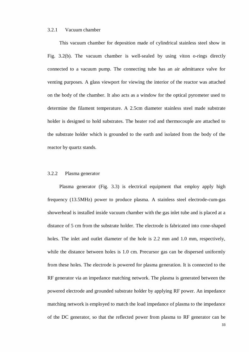
33
3.2.1 Vacuum chamber
This vacuum chamber for deposition made of cylindrical stainless steel show in
Fig. 3.2(b). The vacuum chamber is well-sealed by using viton o-rings directly
connected to a vacuum pump. The connecting tube has an air admittance valve for
venting purposes. A glass viewport for viewing the interior of the reactor was attached
on the body of the chamber. It also acts as a window for the optical pyrometer used to
determine the filament temperature. A 2.5cm diameter stainless steel made substrate
holder is designed to hold substrates. The heater rod and thermocouple are attached to
the substrate holder which is grounded to the earth and isolated from the body of the
reactor by quartz stands.
3.2.2 Plasma generator
Plasma generator (Fig. 3.3) is electrical equipment that employ apply high
frequency (13.5MHz) power to produce plasma. A stainless steel electrode-cum-gas
showerhead is installed inside vacuum chamber with the gas inlet tube and is placed at a
distance of 5 cm from the substrate holder. The electrode is fabricated into cone-shaped
holes. The inlet and outlet diameter of the hole is 2.2 mm and 1.0 mm, respectively,
while the distance between holes is 1.0 cm. Precursor gas can be dispersed uniformly
from these holes. The electrode is powered for plasma generation. It is connected to the
RF generator via an impedance matching network. The plasma is generated between the
powered electrode and grounded substrate holder by applying RF power. An impedance
matching network is employed to match the load impedance of plasma to the impedance
of the DC generator, so that the reflected power from plasma to RF generator can be
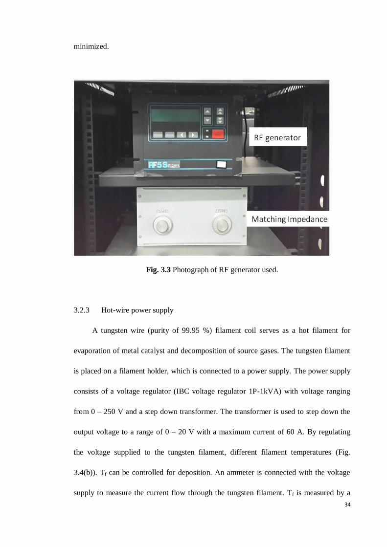
34
minimized.
Fig. 3.3 Photograph of RF generator used.
3.2.3 Hot-wire power supply
A tungsten wire (purity of 99.95 %) filament coil serves as a hot filament for
evaporation of metal catalyst and decomposition of source gases. The tungsten filament
is placed on a filament holder, which is connected to a power supply. The power supply
consists of a voltage regulator (IBC voltage regulator 1P-1kVA) with voltage ranging
from 0 – 250 V and a step down transformer. The transformer is used to step down the
output voltage to a range of 0 – 20 V with a maximum current of 60 A. By regulating
the voltage supplied to the tungsten filament, different filament temperatures (Fig.
3.4(b)). Tf can be controlled for deposition. An ammeter is connected with the voltage
supply to measure the current flow through the tungsten filament. Tf is measured by a
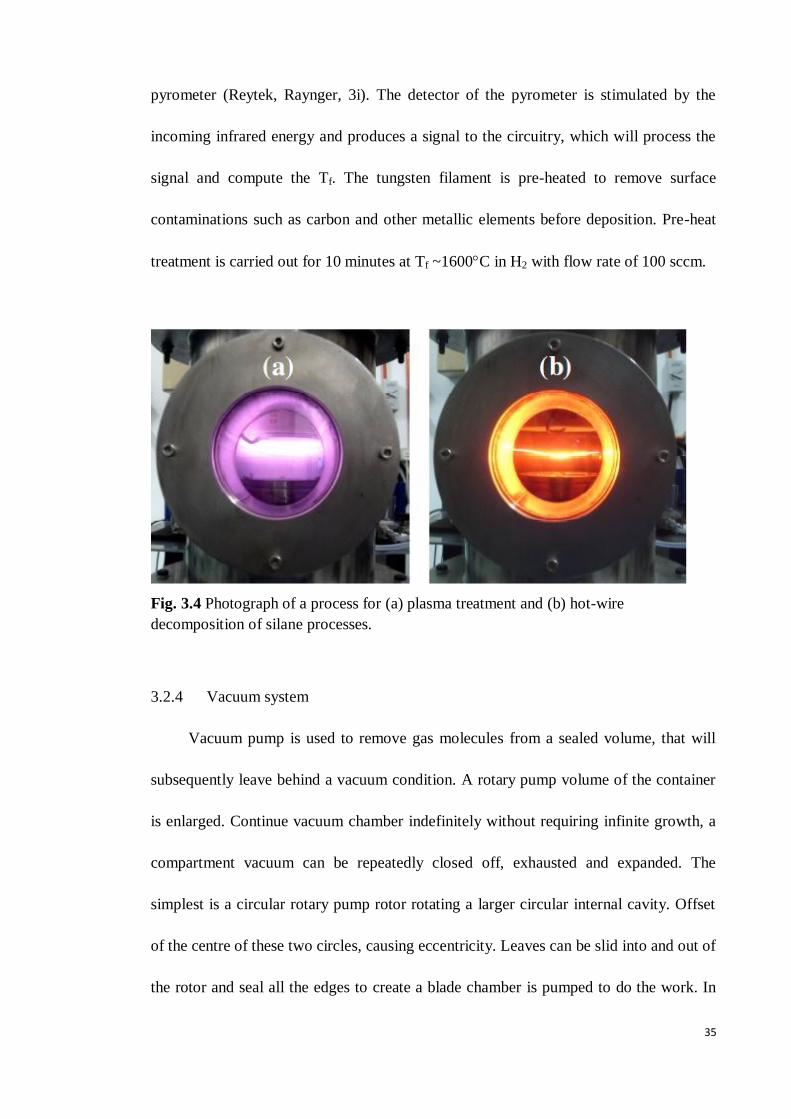
35
pyrometer (Reytek, Raynger, 3i). The detector of the pyrometer is stimulated by the
incoming infrared energy and produces a signal to the circuitry, which will process the
signal and compute the Tf. The tungsten filament is pre-heated to remove surface
contaminations such as carbon and other metallic elements before deposition. Pre-heat
treatment is carried out for 10 minutes at Tf ~1600C in H2 with flow rate of 100 sccm.
Fig. 3.4 Photograph of a process for (a) plasma treatment and (b) hot-wire
decomposition of silane processes.
3.2.4 Vacuum system
Vacuum pump is used to remove gas molecules from a sealed volume, that will
subsequently leave behind a vacuum condition. A rotary pump volume of the container
is enlarged. Continue vacuum chamber indefinitely without requiring infinite growth, a
compartment vacuum can be repeatedly closed off, exhausted and expanded. The
simplest is a circular rotary pump rotor rotating a larger circular internal cavity. Offset
of the centre of these two circles, causing eccentricity. Leaves can be slid into and out of
the rotor and seal all the edges to create a blade chamber is pumped to do the work. In
36
the suction side of the pump, increasing the volume of the vane chamber and filled with
a pressure fluid inlet forced. In the discharge side of the pump, the decrease of the
volume of the blade chambers, thereby forcing fluid out of the pump. Rotary vacuum
pump can reach pressures as low as 10-3
mbar.
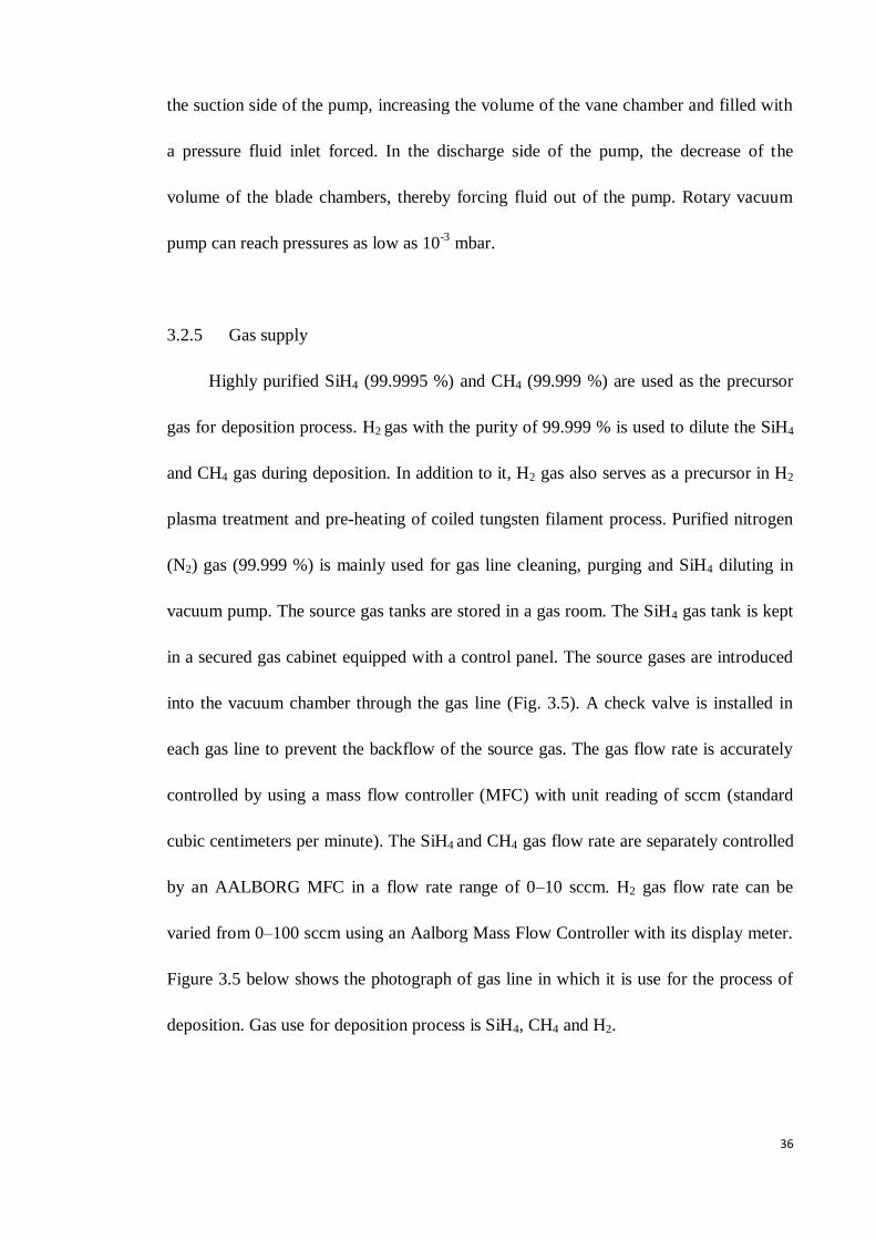
3.2.5 Gas supply
Highly purified SiH4 (99.9995 %) and CH4 (99.999 %) are used as the precursor
gas for deposition process. H2 gas with the purity of 99.999 % is used to dilute the SiH4
and CH4 gas during deposition. In addition to it, H2 gas also serves as a precursor in H2
plasma treatment and pre-heating of coiled tungsten filament process. Purified nitrogen
(N2) gas (99.999 %) is mainly used for gas line cleaning, purging and SiH4 diluting in
vacuum pump. The source gas tanks are stored in a gas room. The SiH4 gas tank is kept
in a secured gas cabinet equipped with a control panel. The source gases are introduced
into the vacuum chamber through the gas line (Fig. 3.5). A check valve is installed in
each gas line to prevent the backflow of the source gas. The gas flow rate is accurately
controlled by using a mass flow controller (MFC) with unit reading of sccm (standard
cubic centimeters per minute). The SiH4 and CH4 gas flow rate are separately controlled
by an AALBORG MFC in a flow rate range of 0–10 sccm. H2 gas flow rate can be
varied from 0–100 sccm using an Aalborg Mass Flow Controller with its display meter.
Figure 3.5 below shows the photograph of gas line in which it is use for the process of
deposition. Gas use for deposition process is SiH4, CH4 and H2.
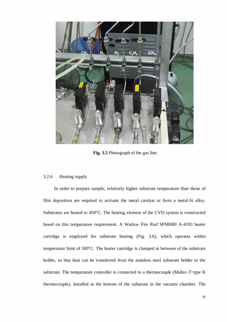
37
Fig. 3.5 Photograph of the gas line.
3.2.6 Heating supply
In order to prepare sample, relatively higher substrate temperature than those of
film deposition are required to activate the metal catalyst or form a metal-Si alloy.
Substrates are heated to 450C. The heating element of the CVD system is constructed
based on this temperature requirement. A Watlow Fire Rod SFMH80 A-4183 heater
cartridge is employed for substrate heating (Fig. 3.6), which operates within
temperature limit of 500C. The heater cartridge is clamped in between of the substrate
holder, so that heat can be transferred from the stainless steel substrate holder to the
substrate. The temperature controller is connected to a thermocouple (Maltec-T type K
thermocouple), installed at the bottom of the substrate in the vacuum chamber. The
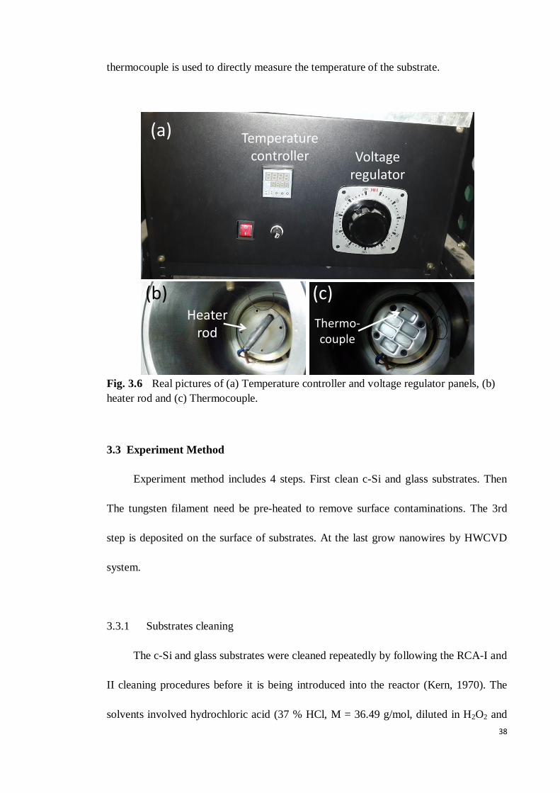
38
thermocouple is used to directly measure the temperature of the substrate.
(a)
(b) (c)
Temperature controller Voltage
regulator
Heater rod
Thermo-couple
Fig. 3.6 Real pictures of (a) Temperature controller and voltage regulator panels, (b)
heater rod and (c) Thermocouple.
3.3 Experiment Method
Experiment method includes 4 steps. First clean c-Si and glass substrates. Then
The tungsten filament need be pre-heated to remove surface contaminations. The 3rd
step is deposited on the surface of substrates. At the last grow nanowires by HWCVD
system.
3.3.1 Substrates cleaning
The c-Si and glass substrates were cleaned repeatedly by following the RCA-I and
II cleaning procedures before it is being introduced into the reactor (Kern, 1970). The
solvents involved hydrochloric acid (37 % HCl, M = 36.49 g/mol, diluted in H2O2 and
39
deionized (DI) water in a ratio of 1:1:6), ammonia (25 % NH4OH, M = 17.03 g/mol,
diluted in H2O2 and DI water in a ratio of 1:1:5). HCl can be used to remove residual
metal contaminations, such as Al, Mg and Zn. NH4OH can be used to remove organic
contaminations and dissolved metal (Au, Ag, Cu, Ni, Cd, Co and Cr) contaminations.
Glass substrates were cleaned using decon 90, acetone (C3H6O, M = 58.08 g/mol),
ethanol (C2H5OH, M = 46.07 g/mol). The glass substrates were immersed in a beaker
containing decon 90 solution and sonicated in ultrasonic bath for 20 minutes to
remove oil and gross dirt contaminations. This was followed by rinsing in acetone;
ethanol and DI water subsequently to remove organic impurities such as the
hydrocarbon dried by N2 purging.
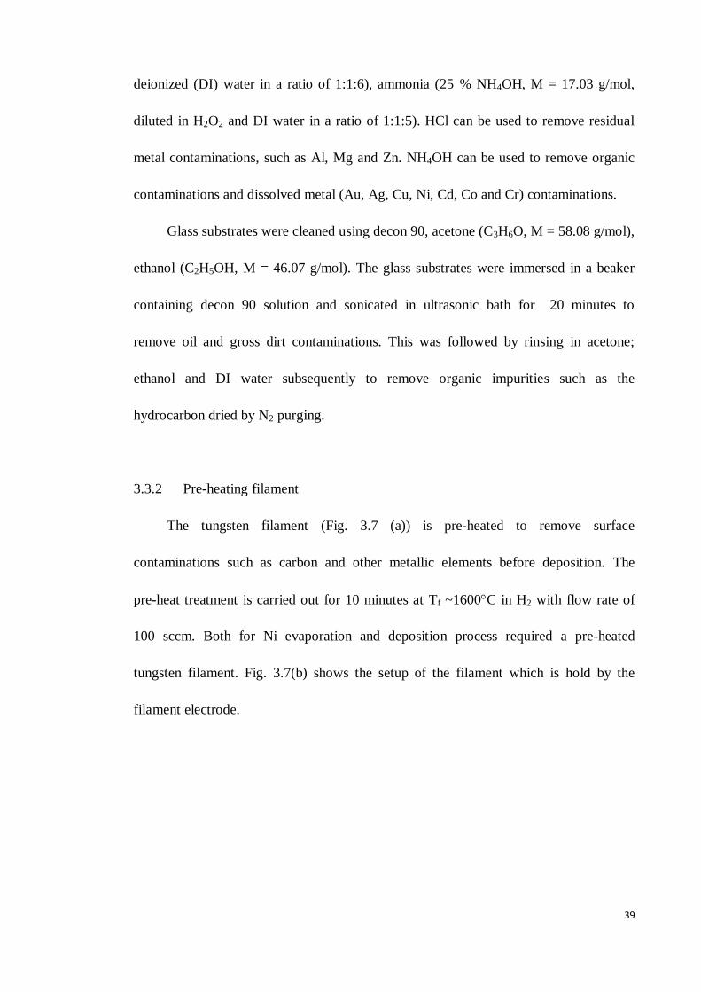
3.3.2 Pre-heating filament
The tungsten filament (Fig. 3.7 (a)) is pre-heated to remove surface
contaminations such as carbon and other metallic elements before deposition. The
pre-heat treatment is carried out for 10 minutes at Tf ~1600C in H2 with flow rate of
100 sccm. Both for Ni evaporation and deposition process required a pre-heated
tungsten filament. Fig. 3.7(b) shows the setup of the filament which is hold by the
filament electrode.
40
(a) (b)
Fig. 3.7 (a) Photograph of tungsten Filament. (b) Photograph of setup of filament for
nickel evaporation and deposition processes. Filament is placed in a filament electrode.
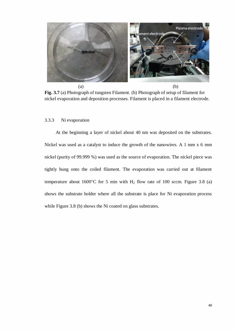
3.3.3 Ni evaporation
At the beginning a layer of nickel about 40 nm was deposited on the substrates.
Nickel was used as a catalyst to induce the growth of the nanowires. A 1 mm x 6 mm
nickel (purity of 99.999 %) was used as the source of evaporation. The nickel piece was
tightly hung onto the coiled filament. The evaporation was carried out at filament
temperature about 1600C for 5 min with H2 flow rate of 100 sccm. Figure 3.8 (a)
shows the substrate holder where all the substrate is place for Ni evaporation process
while Figure 3.8 (b) shows the Ni coated on glass substrates.
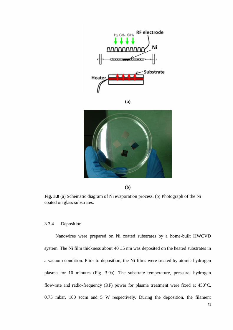
41
(a)
(b)
Fig. 3.8 (a) Schematic diagram of Ni evaporation process. (b) Photograph of the Ni
coated on glass substrates.
3.3.4 Deposition
Nanowires were prepared on Ni coated substrates by a home-built HWCVD
system. The Ni film thickness about 40 ±5 nm was deposited on the heated substrates in
a vacuum condition. Prior to deposition, the Ni films were treated by atomic hydrogen
plasma for 10 minutes (Fig. 3.9a). The substrate temperature, pressure, hydrogen
flow-rate and radio-frequency (RF) power for plasma treatment were fixed at 450C,
0.75 mbar, 100 sccm and 5 W respectively. During the deposition, the filament
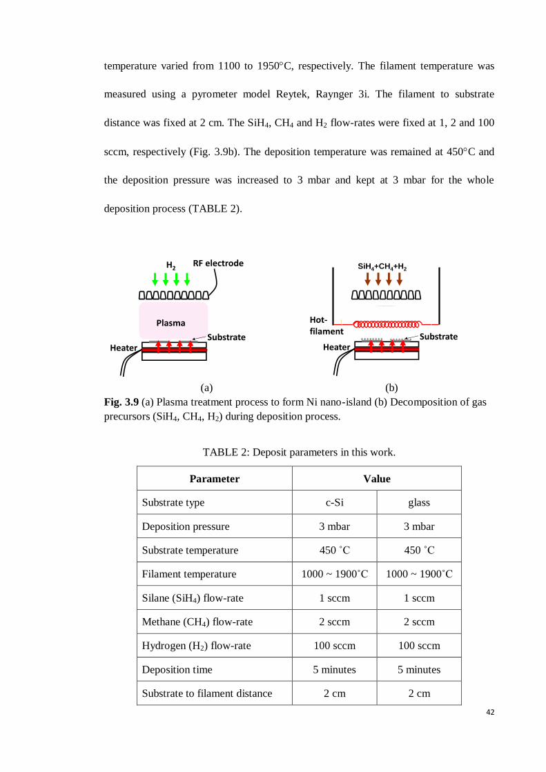
42
temperature varied from 1100 to 1950C, respectively. The filament temperature was
measured using a pyrometer model Reytek, Raynger 3i. The filament to substrate
distance was fixed at 2 cm. The SiH4, CH4 and H2 flow-rates were fixed at 1, 2 and 100
sccm, respectively (Fig. 3.9b). The deposition temperature was remained at 450C and
the deposition pressure was increased to 3 mbar and kept at 3 mbar for the whole
deposition process (TABLE 2).
Plasma
H2
SubstrateHeater
RF electrode
0.2 m
Hot-filament
SiH4+CH4+H2
SubstrateHeater
0.5 m
(a) (b)
Fig. 3.9 (a) Plasma treatment process to form Ni nano-island (b) Decomposition of gas
precursors (SiH4, CH4, H2) during deposition process.
TABLE 2: Deposit parameters in this work.
Parameter Value
Substrate type c-Si glass
Deposition pressure 3 mbar 3 mbar
Substrate temperature 450 ˚C 450 ˚C
Filament temperature 1000 ~ 1900˚C 1000 ~ 1900˚C
Silane (SiH4) flow-rate 1 sccm 1 sccm
Methane (CH4) flow-rate 2 sccm 2 sccm
Hydrogen (H2) flow-rate 100 sccm 100 sccm
Deposition time 5 minutes 5 minutes
Substrate to filament distance 2 cm 2 cm
43
3.4 Characterization Technique
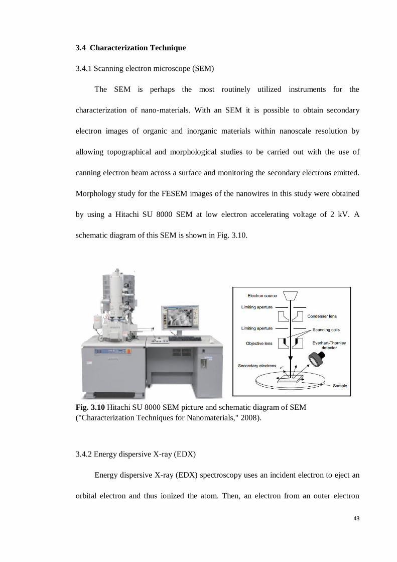
3.4.1 Scanning electron microscope (SEM)
The SEM is perhaps the most routinely utilized instruments for the
characterization of nano-materials. With an SEM it is possible to obtain secondary
electron images of organic and inorganic materials within nanoscale resolution by
allowing topographical and morphological studies to be carried out with the use of
canning electron beam across a surface and monitoring the secondary electrons emitted.
Morphology study for the FESEM images of the nanowires in this study were obtained
by using a Hitachi SU 8000 SEM at low electron accelerating voltage of 2 kV. A
schematic diagram of this SEM is shown in Fig. 3.10.
Fig. 3.10 Hitachi SU 8000 SEM picture and schematic diagram of SEM
("Characterization Techniques for Nanomaterials," 2008).
3.4.2 Energy dispersive X-ray (EDX)
Energy dispersive X-ray (EDX) spectroscopy uses an incident electron to eject an
orbital electron and thus ionized the atom. Then, an electron from an outer electron
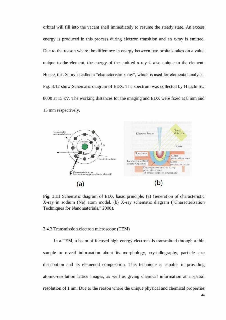
44
orbital will fill into the vacant shell immediately to resume the steady state. An excess
energy is produced in this process during electron transition and an x-ray is emitted.
Due to the reason where the difference in energy between two orbitals takes on a value
unique to the element, the energy of the emitted x-ray is also unique to the element.
Hence, this X-ray is called a “characteristic x-ray”, which is used for elemental analysis.
Fig. 3.12 show Schematic diagram of EDX. The spectrum was collected by Hitachi SU
8000 at 15 kV. The working distances for the imaging and EDX were fixed at 8 mm and
15 mm respectively.
Fig. 3.11 Schematic diagram of EDX basic principle. (a) Generation of characteristic
X-ray in sodium (Na) atom model. (b) X-ray schematic diagram ("Characterization
Techniques for Nanomaterials," 2008).
3.4.3 Transmission electron microscope (TEM)
In a TEM, a beam of focused high energy electrons is transmitted through a thin
sample to reveal information about its morphology, crystallography, particle size
distribution and its elemental composition. This technique is capable in providing
atomic-resolution lattice images, as well as giving chemical information at a spatial
resolution of 1 nm. Due to the reason where the unique physical and chemical properties
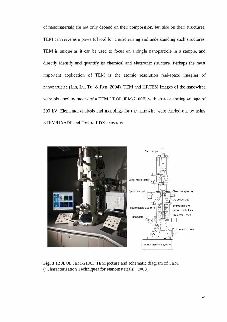
45
of nanomaterials are not only depend on their composition, but also on their structures,
TEM can serve as a powerful tool for characterizing and understanding such structures.
TEM is unique as it can be used to focus on a single nanoparticle in a sample, and
directly identify and quantify its chemical and electronic structure. Perhaps the most
important application of TEM is the atomic resolution real-space imaging of
nanoparticles (Lin, Lu, Tu, & Ren, 2004). TEM and HRTEM images of the nanowires
were obtained by means of a TEM (JEOL JEM-2100F) with an accelerating voltage of
200 kV. Elemental analysis and mappings for the nanowire were carried out by using
STEM/HAADF and Oxford EDX detectors.
Fig. 3.12 JEOL JEM-2100F TEM picture and schematic diagram of TEM
("Characterization Techniques for Nanomaterials," 2008).
46
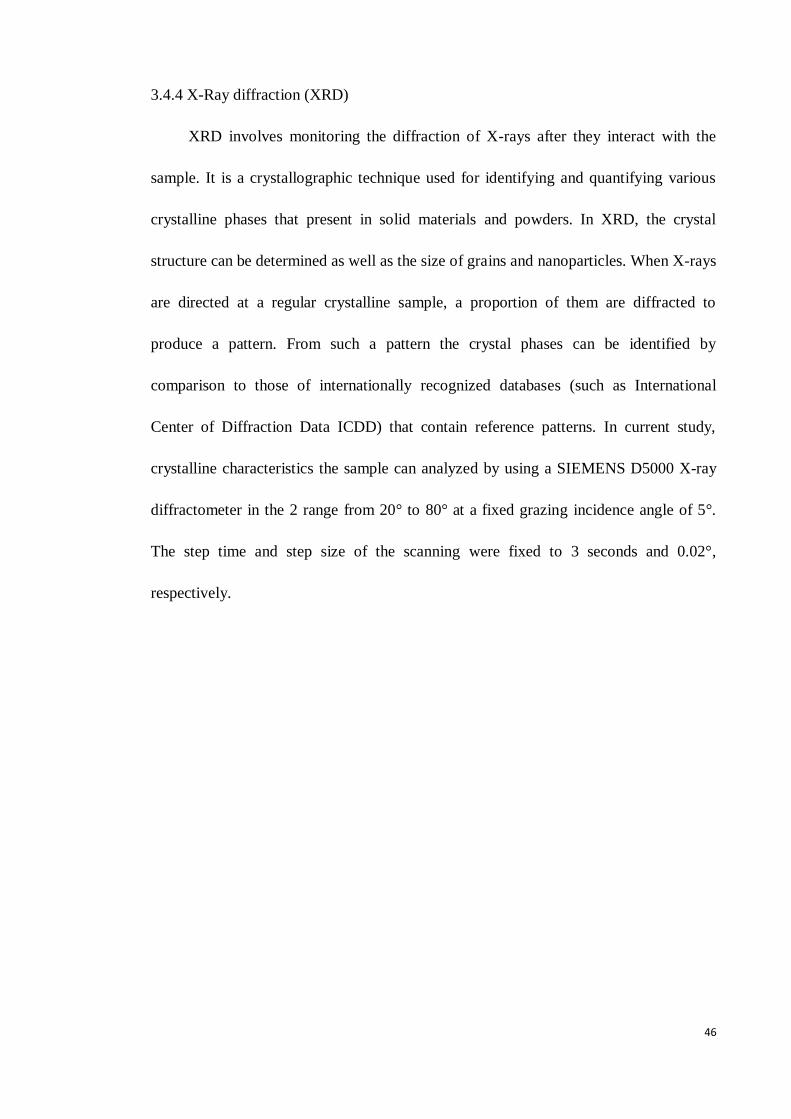
3.4.4 X-Ray diffraction (XRD)
XRD involves monitoring the diffraction of X-rays after they interact with the
sample. It is a crystallographic technique used for identifying and quantifying various
crystalline phases that present in solid materials and powders. In XRD, the crystal
structure can be determined as well as the size of grains and nanoparticles. When X-rays
are directed at a regular crystalline sample, a proportion of them are diffracted to
produce a pattern. From such a pattern the crystal phases can be identified by
comparison to those of internationally recognized databases (such as International
Center of Diffraction Data ICDD) that contain reference patterns. In current study,
crystalline characteristics the sample can analyzed by using a SIEMENS D5000 X-ray
diffractometer in the 2 range from 20° to 80° at a fixed grazing incidence angle of 5°.
The step time and step size of the scanning were fixed to 3 seconds and 0.02°,
respectively.
47
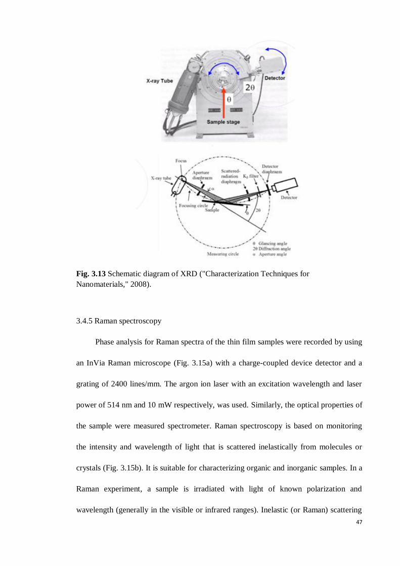
Fig. 3.13 Schematic diagram of XRD ("Characterization Techniques for
Nanomaterials," 2008).
3.4.5 Raman spectroscopy
Phase analysis for Raman spectra of the thin film samples were recorded by using
an InVia Raman microscope (Fig. 3.15a) with a charge-coupled device detector and a
grating of 2400 lines/mm. The argon ion laser with an excitation wavelength and laser
power of 514 nm and 10 mW respectively, was used. Similarly, the optical properties of
the sample were measured spectrometer. Raman spectroscopy is based on monitoring
the intensity and wavelength of light that is scattered inelastically from molecules or
crystals (Fig. 3.15b). It is suitable for characterizing organic and inorganic samples. In a
Raman experiment, a sample is irradiated with light of known polarization and
wavelength (generally in the visible or infrared ranges). Inelastic (or Raman) scattering
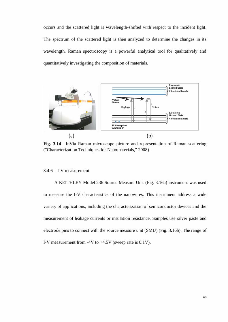
48
occurs and the scattered light is wavelength-shifted with respect to the incident light.
The spectrum of the scattered light is then analyzed to determine the changes in its
wavelength. Raman spectroscopy is a powerful analytical tool for qualitatively and
quantitatively investigating the composition of materials.
Fig. 3.14 InVia Raman microscope picture and representation of Raman scattering
("Characterization Techniques for Nanomaterials," 2008).
3.4.6 I-V measurement
A KEITHLEY Model 236 Source Measure Unit (Fig. 3.16a) instrument was used
to measure the I-V characteristics of the nanowires. This instrument address a wide
variety of applications, including the characterization of semiconductor devices and the
measurement of leakage currents or insulation resistance. Samples use silver paste and
electrode pins to connect with the source measure unit (SMU) (Fig. 3.16b). The range of
I-V measurement from -4V to +4.5V (sweep rate is 0.1V).
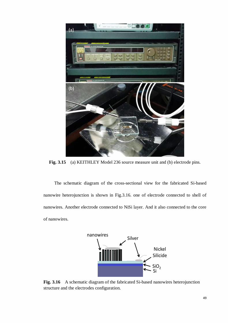
49
Fig. 3.15 (a) KEITHLEY Model 236 source measure unit and (b) electrode pins.
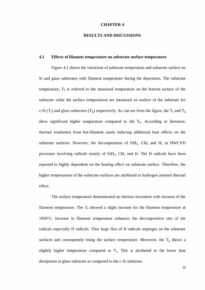
The schematic diagram of the cross-sectional view for the fabricated Si-based
nanowire heterojunction is shown in Fig.3.16. one of electrode connected to shell of
nanowires. Another electrode connected to NiSi layer. And it also connected to the core
of nanowires.
Silver nanowires
Nickel Silicide
SiO2Si
(a)
Fig. 3.16 A schematic diagram of the fabricated Si-based nanowires heterojunction
structure and the electrodes configuration.
50
CHAPTER 4
RESULTS AND DISCUSSIONS
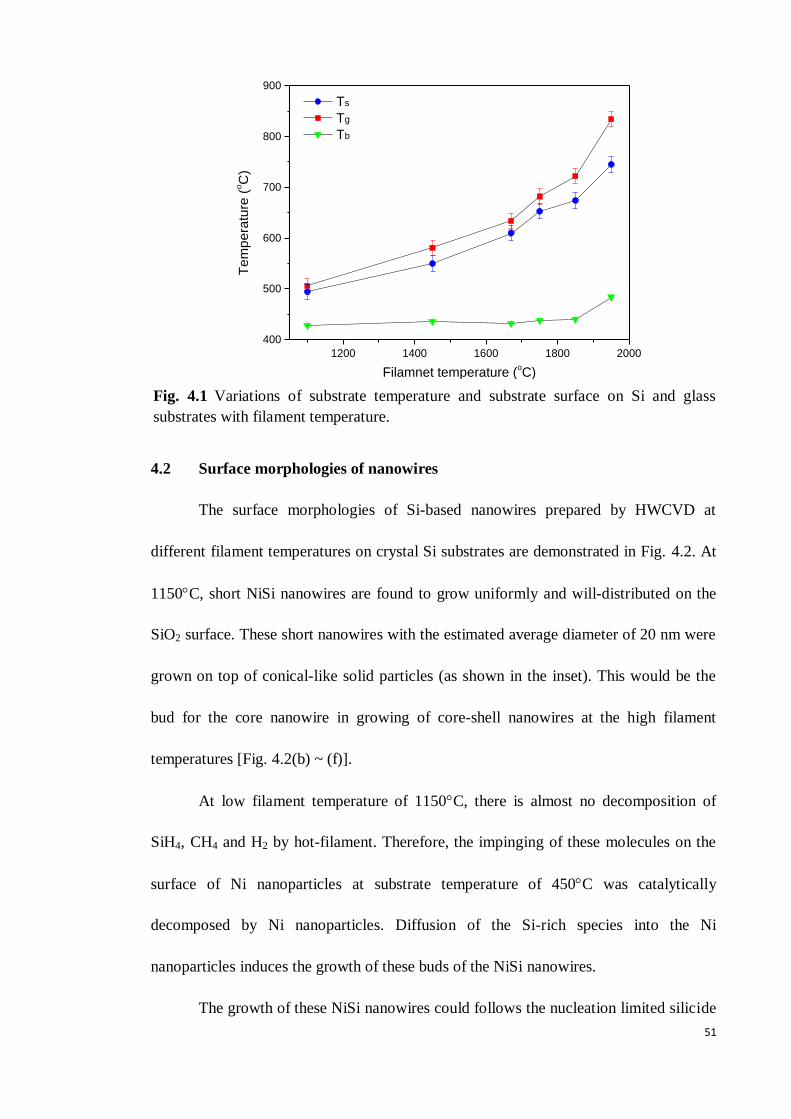
4.1 Effects of filament temperature on substrate surface temperature
Figure 4.1 shows the variations of substrate temperature and substrate surface on
Si and glass substrates with filament temperature during the deposition. The substrate
temperature, Tb is referred to the measured temperature on the bottom surface of the
substrate while the surface temperatures are measured on surface of the substrate for
c-Si (Ts) and glass substrates (Tg) respectively. As can see from the figure, the Ts and Tg
show significant higher temperature compared to the Tb. According to literature,
thermal irradiation from hot-filament easily inducing additional heat effects on the
substrate surfaces. However, the decomposition of SiH4, CH4 and H2 in HWCVD
processes involving radicals mainly of SiH3, CH3 and H. The H radicals have been
reported to highly dependent on the heating effect on substrate surface. Therefore, the
higher temperatures of the substrate surfaces are attributed to hydrogen assisted thermal
effect.
The surface temperature demonstrated an obvious increment with increase of the
filament temperature. The Tb showed a slight increase for the filament temperature at
1950C. Increase in filament temperature enhances the decomposition rate of the
radicals especially H radicals. Thus large flux of H radicals impinges on the substrate
surfaces and consequently rising the surface temperature. Moreover, the Tg shows a
slightly higher temperature compared to Ts. This is attributed to the lower heat
dissipation in glass substrate as compared to the c-Si substrate.
51
1200 1400 1600 1800 2000
400
500
600
700
800
900
Te
mp
era
ture
(oC
)
Filamnet temperature (oC)
Ts
Tg
Tb
Fig. 4.1 Variations of substrate temperature and substrate surface on Si and glass
substrates with filament temperature.
4.2 Surface morphologies of nanowires
The surface morphologies of Si-based nanowires prepared by HWCVD at
different filament temperatures on crystal Si substrates are demonstrated in Fig. 4.2. At
1150C, short NiSi nanowires are found to grow uniformly and will-distributed on the
SiO2 surface. These short nanowires with the estimated average diameter of 20 nm were
grown on top of conical-like solid particles (as shown in the inset). This would be the
bud for the core nanowire in growing of core-shell nanowires at the high filament
temperatures [Fig. 4.2(b) ~ (f)].
At low filament temperature of 1150C, there is almost no decomposition of
SiH4, CH4 and H2 by hot-filament. Therefore, the impinging of these molecules on the
surface of Ni nanoparticles at substrate temperature of 450C was catalytically
decomposed by Ni nanoparticles. Diffusion of the Si-rich species into the Ni
nanoparticles induces the growth of these buds of the NiSi nanowires.
The growth of these NiSi nanowires could follows the nucleation limited silicide
52
reaction which has been described by Kim et al. (J. Kim & Anderson, 2005). Increase in
filament temperature to 1450C, high density of rod-like Si nanowires is clearly
presented in Fig. 4.2(b). These nanowires demonstrated a grainy surface morphology as
demonstrated in the inset figure. The estimated average diameter and length of these
nanowires are typically 400 nm and 2 m respectively that measured in Fig. 4.2.
At filament temperatures 1450C and above, the hot-filament is able to
decompose the SiH4 and H2 efficiently (Tange et al., 2001). High decomposition rates
of SiH4 and H2 lead to deposition of high density of Si-rich species onto the surface of
Ni nanoparticles. This increases the diffusion of Si-rich species into the Ni nanoparticles
thus enhances the precipitation of Si nanowires. On the other hand, deposition of the
decomposed radicals mainly SiH3 on the sidewalls of the nanowires leads to the radial
growth of the Si grains as shown by the grainy morphology in the figure. This
morphology is significant for the nanowires at 1650C.
Further increase in filament temperature to 1750C and above has resultant in
drastical changes in the morphology of the nanowires. These nanowires demonstrated a
smooth surface and irregular array. Furthermore, these nanowires exhibited longer and
slimmer in length and diameter, respectively. At filament temperature of 1750C, the
estimated average diameter and length are 70 nm and 4 m respectively. As presented
by Dasgupta et al. (Tange et al., 2001), filament temperature above 1750C
demonstrated sufficiently decomposition of SiH4, H2 and CH4 molecules. In this case,
additional diffusion of the C-rich species could easily limit the radial growth of Si
nanocolumns which has been reported in our previous work (Chong, Dee, Yahya, &
Rahman, 2013; Chong et al., 2011). The formation of SiC as a shell layer could easily
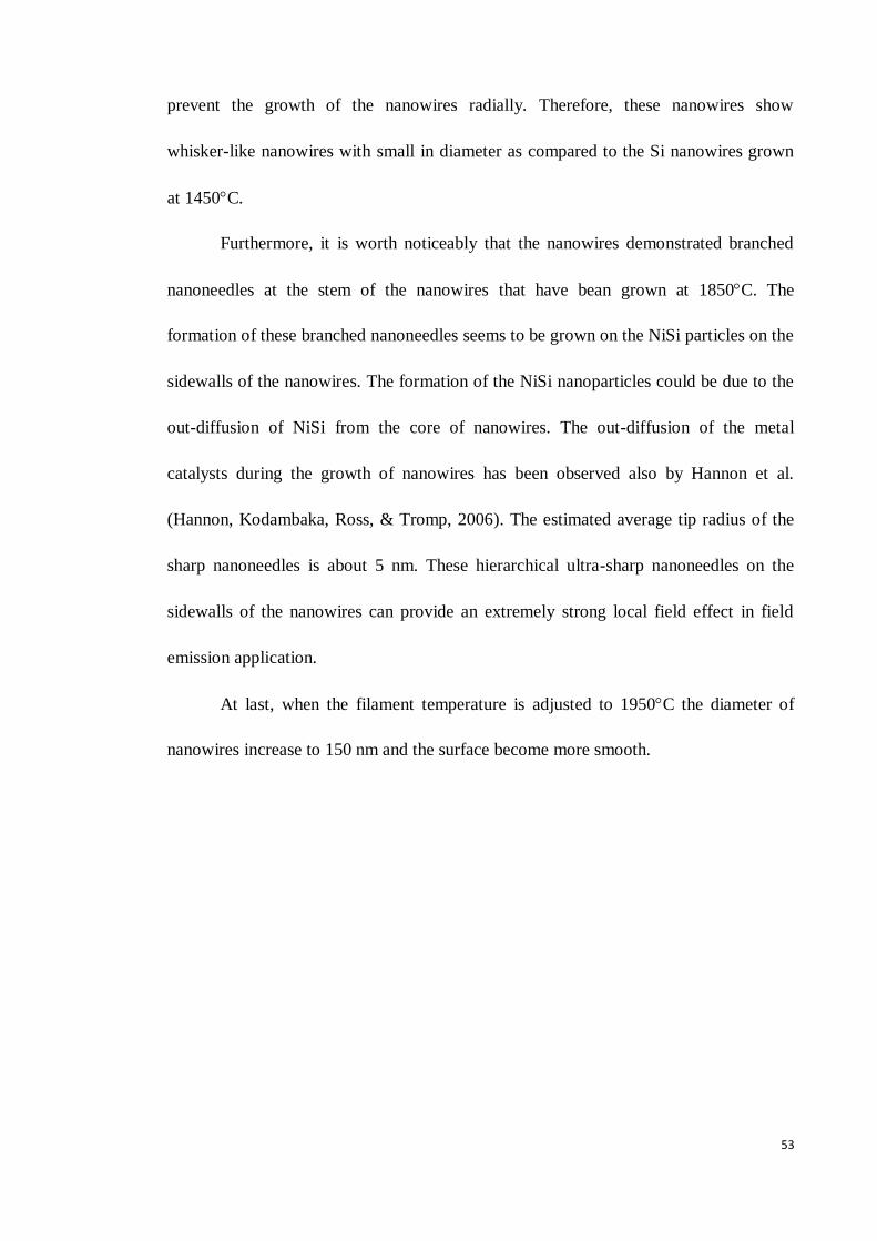
53
prevent the growth of the nanowires radially. Therefore, these nanowires show
whisker-like nanowires with small in diameter as compared to the Si nanowires grown
at 1450C.
Furthermore, it is worth noticeably that the nanowires demonstrated branched
nanoneedles at the stem of the nanowires that have bean grown at 1850C. The
formation of these branched nanoneedles seems to be grown on the NiSi particles on the
sidewalls of the nanowires. The formation of the NiSi nanoparticles could be due to the
out-diffusion of NiSi from the core of nanowires. The out-diffusion of the metal
catalysts during the growth of nanowires has been observed also by Hannon et al.
(Hannon, Kodambaka, Ross, & Tromp, 2006). The estimated average tip radius of the
sharp nanoneedles is about 5 nm. These hierarchical ultra-sharp nanoneedles on the
sidewalls of the nanowires can provide an extremely strong local field effect in field
emission application.
At last, when the filament temperature is adjusted to 1950C the diameter of
nanowires increase to 150 nm and the surface become more smooth.
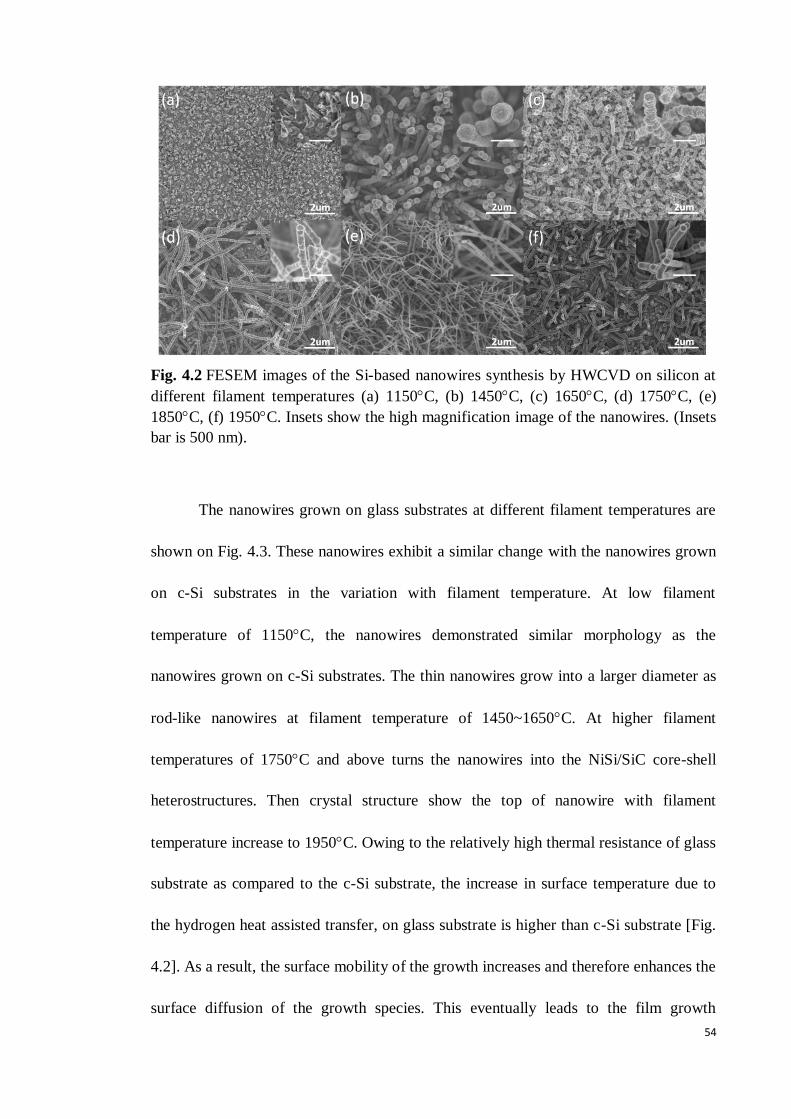
54
Fig. 4.2 FESEM images of the Si-based nanowires synthesis by HWCVD on silicon at
different filament temperatures (a) 1150C, (b) 1450C, (c) 1650C, (d) 1750C, (e)
1850C, (f) 1950C. Insets show the high magnification image of the nanowires. (Insets
bar is 500 nm).
The nanowires grown on glass substrates at different filament temperatures are
shown on Fig. 4.3. These nanowires exhibit a similar change with the nanowires grown
on c-Si substrates in the variation with filament temperature. At low filament
temperature of 1150C, the nanowires demonstrated similar morphology as the
nanowires grown on c-Si substrates. The thin nanowires grow into a larger diameter as
rod-like nanowires at filament temperature of 1450~1650C. At higher filament
temperatures of 1750C and above turns the nanowires into the NiSi/SiC core-shell
heterostructures. Then crystal structure show the top of nanowire with filament
temperature increase to 1950C. Owing to the relatively high thermal resistance of glass
substrate as compared to the c-Si substrate, the increase in surface temperature due to
the hydrogen heat assisted transfer, on glass substrate is higher than c-Si substrate [Fig.
4.2]. As a result, the surface mobility of the growth increases and therefore enhances the
surface diffusion of the growth species. This eventually leads to the film growth
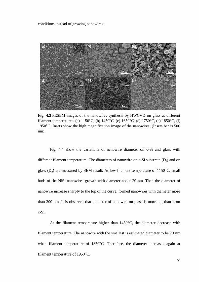
55
conditions instead of growing nanowires.
Fig. 4.3 FESEM images of the nanowires synthesis by HWCVD on glass at different
filament temperatures. (a) 1150C, (b) 1450C, (c) 1650C, (d) 1750C, (e) 1850C, (f)
1950C. Insets show the high magnification image of the nanowires. (Insets bar is 500
nm).
Fig. 4.4 show the variations of nanowire diameter on c-Si and glass with
different filament temperature. The diameters of nanowire on c-Si substrate (Ds) and on
glass (Dg) are measured by SEM result. At low filament temperature of 1150C, small
buds of the NiSi nanowires growth with diameter about 20 nm. Then the diameter of
nanowire increase sharply to the top of the curve, formed nanowires with diameter more
than 300 nm. It is observed that diameter of nanowire on glass is more big than it on
c-Si..
At the filament temperature higher than 1450C, the diameter decrease with
filament temperature. The nanowire with the smallest is estimated diameter to be 70 nm
when filament temperature of 1850C. Therefore, the diameter increases again at
filament temperature of 1950C.
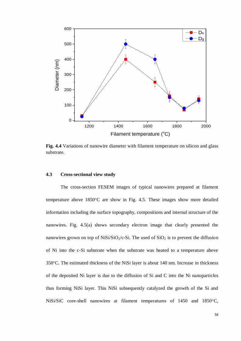
56
1200 1400 1600 1800 2000
0
100
200
300
400
500
600
Dia
me
ter
(nm
)
Filament temperature (oC)
Ds
Dg
Fig. 4.4 Variations of nanowire diameter with filament temperature on silicon and glass
substrate.
4.3 Cross-sectional view study
The cross-section FESEM images of typical nanowires prepared at filament
temperature above 1850C are show in Fig. 4.5. These images show more detailed
information including the surface topography, compositions and internal structure of the
nanowires. Fig. 4.5(a) shows secondary electron image that clearly presented the
nanowires grown on top of NiSi/SiO2/c-Si. The used of SiO2 is to prevent the diffusion
of Ni into the c-Si substrate when the substrate was heated to a temperature above
350C. The estimated thickness of the NiSi layer is about 140 nm. Increase in thickness
of the deposited Ni layer is due to the diffusion of Si and C into the Ni nanoparticles
thus forming NiSi layer. This NiSi subsequently catalyzed the growth of the Si and
NiSi/SiC core-shell nanowires at filament temperatures of 1450 and 1850C,
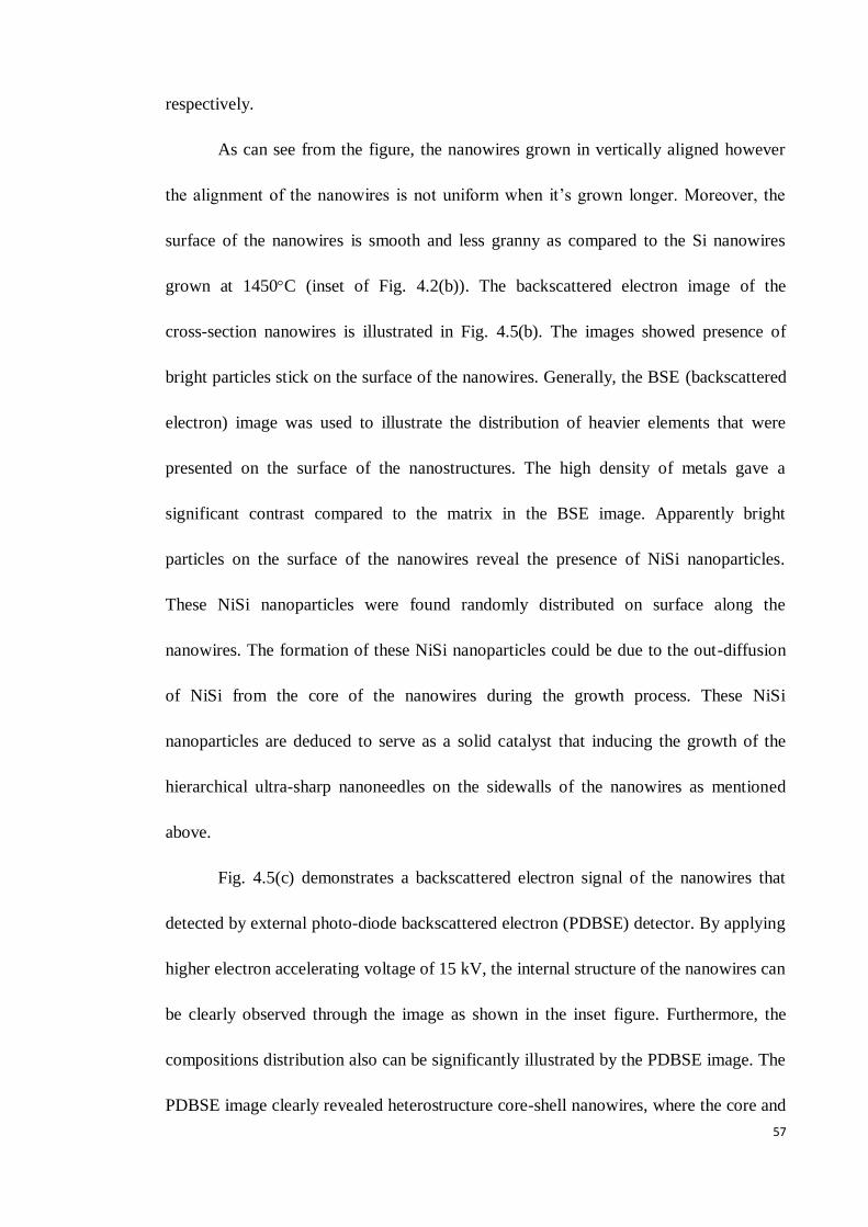
57
respectively.
As can see from the figure, the nanowires grown in vertically aligned however
the alignment of the nanowires is not uniform when it’s grown longer. Moreover, the
surface of the nanowires is smooth and less granny as compared to the Si nanowires
grown at 1450C (inset of Fig. 4.2(b)). The backscattered electron image of the
cross-section nanowires is illustrated in Fig. 4.5(b). The images showed presence of
bright particles stick on the surface of the nanowires. Generally, the BSE (backscattered
electron) image was used to illustrate the distribution of heavier elements that were
presented on the surface of the nanostructures. The high density of metals gave a
significant contrast compared to the matrix in the BSE image. Apparently bright
particles on the surface of the nanowires reveal the presence of NiSi nanoparticles.
These NiSi nanoparticles were found randomly distributed on surface along the
nanowires. The formation of these NiSi nanoparticles could be due to the out-diffusion
of NiSi from the core of the nanowires during the growth process. These NiSi
nanoparticles are deduced to serve as a solid catalyst that inducing the growth of the
hierarchical ultra-sharp nanoneedles on the sidewalls of the nanowires as mentioned
above.
Fig. 4.5(c) demonstrates a backscattered electron signal of the nanowires that
detected by external photo-diode backscattered electron (PDBSE) detector. By applying
higher electron accelerating voltage of 15 kV, the internal structure of the nanowires can
be clearly observed through the image as shown in the inset figure. Furthermore, the
compositions distribution also can be significantly illustrated by the PDBSE image. The
PDBSE image clearly revealed heterostructure core-shell nanowires, where the core and
58
shell are attributed to NiSi and SiC respectively. Moreover, the NiSi core can be clearly
presented along the nanowires from the root to the tip. The formation of the NiSi
nanoparticles also clearly presented on the surface along the nanowires. On the other
hand, these nanowires are grown on top of NiSi layer and the core nanowires are tightly
connected to the NiSi layer, which could be a good electrical contact for energy storage
applications such as lithium-ion batteries and micro-supercapacitor electrodes. An
extremely large surface area of the nanowires is expected to enhance the performance of
these devices.
Fig. 4.5 Cross-sectional view of FESEM images of the nanowires prepared by HWCVD
at filament temperature of 1850C. (a) secondary electron (b) backscattered electron
signals (c) backscattered electron signal collected by a photo-diode backscattered electron
(PDBSE) detector that attached to the SEM. Insets figures present high magnification of
the FESEM images.
59
4.4 Microstructure study
The microstructures of the nanowires were investigated by HRTEM and the
result for the samples that have been grown at filament temperatures of 1450 and
1850C are show in Fig. 4.6 and Fig. 4.7, respectively. These nanowires were prepared
on top of a carbon film that has been supported by a TEM copper-grid as demonstrated
in the TEM images.
According to Fig. 4.6, the nanowire exhibits a flower-like morphology with a
core-shell structure. The formation of the flower branches implies that the radial growth
has take place which transform into nanocolumns and ultimately led to the branching
topology. The diameter and thickness of the core and shell are estimated to be 10 and
130 nm, respectively. There is no obvious tapered morphology observed on the
nanowire, which indicates that the shell was grown along the axis of the nanowires that
are parallel with the core.
Fig. 4.6(b) shows a HRTEM image that was obtained at the sidewall of
nanowire, which reveals a polycrystalline structure of the nano columns. The estimated
spacing was estimated to be approximately 0.31 nm, which is corresponds to Si (111)
crystallographic plane [JCPDS card no: 78-2500]. The crystal orientation is further
revealed by the Fast Fourier Transform (FFT) as shown in the inset image.
The polycrystalline Si that formed nanocolumns can be observed in Fig. 4.6(d).
The estimated diameter of these nanocolumns is approximately to be in the range
between 20 and 24 nm. The formation of these nanocolumns follows the preferred
orientation of Si (111) crystalline plane and also the growth direction as well.
Furthermore, a thin amorphous layer can be clearly observed on the outer layer of the
60
nanowire, which indicates the indicating a formation of thin amorphous SiOx that could
be attributed to an oxidation on the nanowire surface after exposed to ambient. The
estimated thickness of the amorphous SiOx layer was approximately 3.4 nm.
Fig. 4.6(c) depicts a HRTEM image along the edge of the core for a nanowire,
which clearly reveals a single crystalline core and a polycrystalline shell heterostructure.
The lattice spacing is approximately estimated to be 0.33 nm and well, correspond to a
crystallographic plane of Ni3Si2 (112) orientation [JCPDS card no: 89-7167]. This
indicates that the core of the nanowires was actually formed by a single crystalline
Ni3Si2 nanowire. The single crystalline Ni3Si2 structure of the core of nanowire was
further revealed by an FFT as shown in the inset. Furthermore, the FFT result reveals
the growth of these Ni3Si2 core nanowires are oriented along the (112) crystal plane.
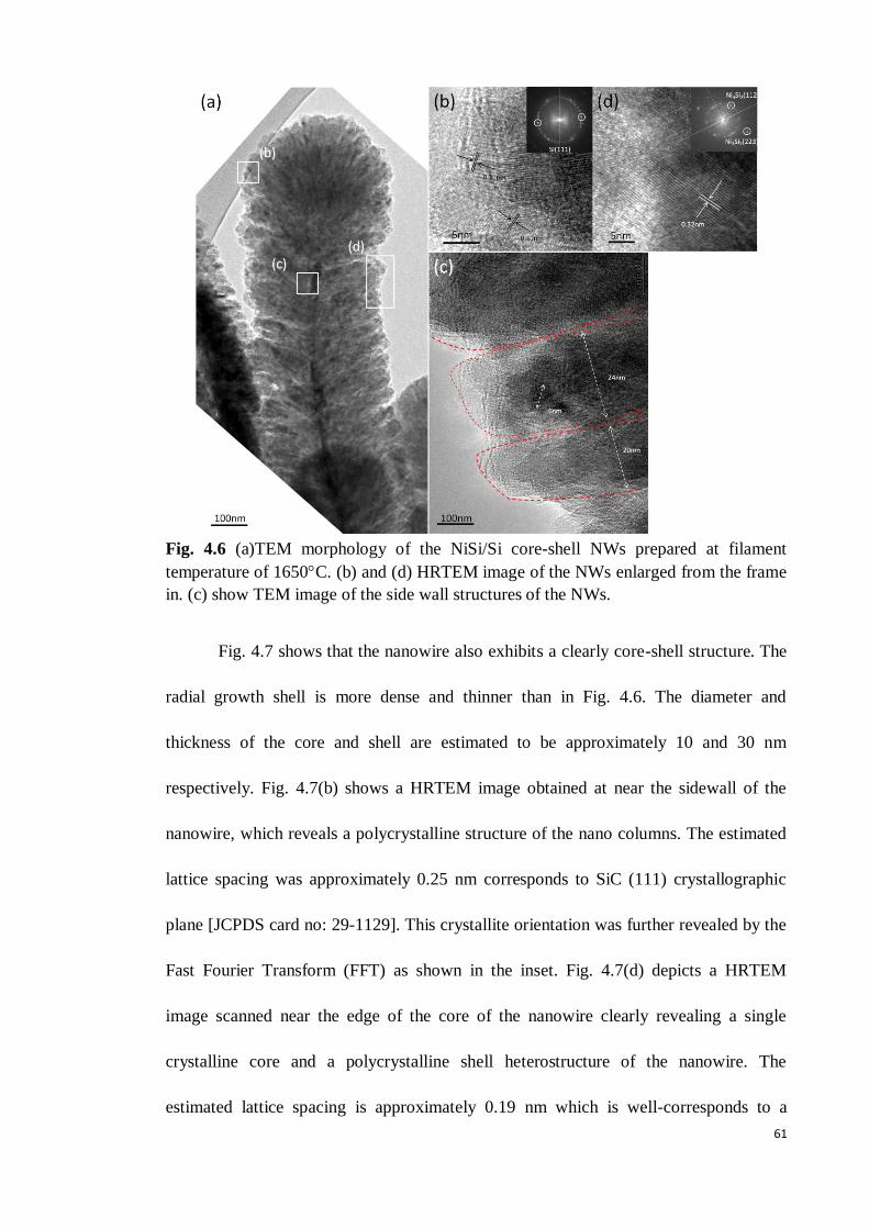
61
Fig. 4.6 (a)TEM morphology of the NiSi/Si core-shell NWs prepared at filament
temperature of 1650C. (b) and (d) HRTEM image of the NWs enlarged from the frame
in. (c) show TEM image of the side wall structures of the NWs.
Fig. 4.7 shows that the nanowire also exhibits a clearly core-shell structure. The
radial growth shell is more dense and thinner than in Fig. 4.6. The diameter and
thickness of the core and shell are estimated to be approximately 10 and 30 nm
respectively. Fig. 4.7(b) shows a HRTEM image obtained at near the sidewall of the
nanowire, which reveals a polycrystalline structure of the nano columns. The estimated
lattice spacing was approximately 0.25 nm corresponds to SiC (111) crystallographic
plane [JCPDS card no: 29-1129]. This crystallite orientation was further revealed by the
Fast Fourier Transform (FFT) as shown in the inset. Fig. 4.7(d) depicts a HRTEM
image scanned near the edge of the core of the nanowire clearly revealing a single
crystalline core and a polycrystalline shell heterostructure of the nanowire. The
estimated lattice spacing is approximately 0.19 nm which is well-corresponds to a
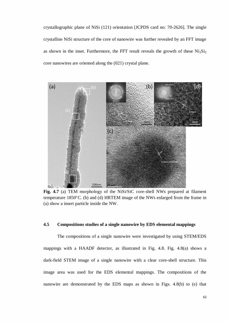
62
crystallographic plane of NiSi (121) orientation [JCPDS card no: 70-2626]. The single
crystalline NiSi structure of the core of nanowire was further revealed by an FFT image
as shown in the inset. Furthermore, the FFT result reveals the growth of these Ni3Si2
core nanowires are oriented along the (021) crystal plane.
Fig. 4.7 (a) TEM morphology of the NiSi/SiC core-shell NWs prepared at filament
temperature 1850C. (b) and (d) HRTEM image of the NWs enlarged from the frame in
(a) show a insert particle inside the NW.
4.5 Compositions studies of a single nanowire by EDS elemental mappings
The compositions of a single nanowire were investigated by using STEM/EDS
mappings with a HAADF detector, as illustrated in Fig. 4.8. Fig. 4.8(a) shows a
dark-field STEM image of a single nanowire with a clear core-shell structure. This
image area was used for the EDS elemental mappings. The compositions of the
nanowire are demonstrated by the EDS maps as shown in Figs. 4.8(b) to (e) that
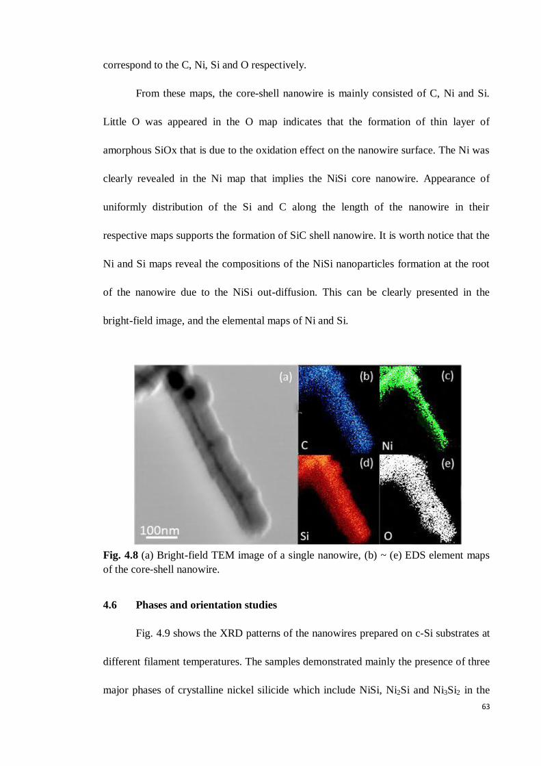
63
correspond to the C, Ni, Si and O respectively.
From these maps, the core-shell nanowire is mainly consisted of C, Ni and Si.
Little O was appeared in the O map indicates that the formation of thin layer of
amorphous SiOx that is due to the oxidation effect on the nanowire surface. The Ni was
clearly revealed in the Ni map that implies the NiSi core nanowire. Appearance of
uniformly distribution of the Si and C along the length of the nanowire in their
respective maps supports the formation of SiC shell nanowire. It is worth notice that the
Ni and Si maps reveal the compositions of the NiSi nanoparticles formation at the root
of the nanowire due to the NiSi out-diffusion. This can be clearly presented in the
bright-field image, and the elemental maps of Ni and Si.
Fig. 4.8 (a) Bright-field TEM image of a single nanowire, (b) ~ (e) EDS element maps
of the core-shell nanowire.
4.6 Phases and orientation studies
Fig. 4.9 shows the XRD patterns of the nanowires prepared on c-Si substrates at
different filament temperatures. The samples demonstrated mainly the presence of three
major phases of crystalline nickel silicide which include NiSi, Ni2Si and Ni3Si2 in the
64
sample. Crystalline NiSi with the orientation of (211) plane seems to be dominant
among the phases. This indicates that the NiSi core could be in (211) growth direction.
Instead of NiSi, other phases of NiSi could be from the NiSi nanoparticles that presence
on the surface along the nanowires. Since the formation of the NiSi nanoparticles is
random therefore its cause to the formation of different crystalline planes.
Furthermore, crystalline Si peaks were observed at diffraction angles of 28.4 and
56.3 which are correspond to crystalline Si (111) and (311) planes respectively. At
highest filament temperature of 1850C, a small and broad peak was detected at
diffraction angle of 35.7 which attributed to crystalline 3C-SiC with a crystalline
orientation of (111) plane. The crystalline size of the SiC nano-crystallites can be
estimated by using Scherrer’s equation as D=kλ/(βcosθ), where k λ, β and θ are
corresponding to the Scherrer’s constant (0.9), wavelength of X-ray (1.5089 Å),
full-width half-maximum of the diffraction peak and Bragg angle of the diffraction peak
respectively (Goh, Wah, Aspanut, & Rahman, 2014). The average crystallite size of the
SiC nano-crystallites is about 3 nm. By rough estimation from the PDBSE image, the
diameter of the core and shell is about 7 and 70 nm respectively. Therefore, the
presence SiC nano-crystallites most probably embedded within an amorphous matrix in
the shell of the nanowires.
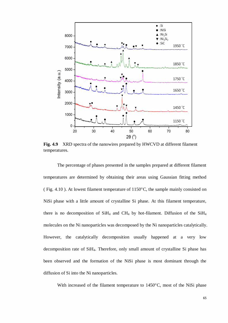
65
Fig. 4.9 XRD spectra of the nanowires prepared by HWCVD at different filament
temperatures.
The percentage of phases presented in the samples prepared at different filament
temperatures are determined by obtaining their areas using Gaussian fitting method
( Fig. 4.10 ). At lowest filament temperature of 1150C, the sample mainly consisted on
NiSi phase with a little amount of crystalline Si phase. At this filament temperature,
there is no decomposition of SiH4 and CH4 by hot-filament. Diffusion of the SiH4
molecules on the Ni nanoparticles was decomposed by the Ni nanoparticles catalytically.
However, the catalytically decomposition usually happened at a very low
decomposition rate of SiH4. Therefore, only small amount of crystalline Si phase has
been observed and the formation of the NiSi phase is most dominant through the
diffusion of Si into the Ni nanoparticles.
With increased of the filament temperature to 1450C, most of the NiSi phase
66
are converted to Ni3Si2 and the percentage of crystalline Si phase increases. This could
be the reason for the growth of Si nanowires which catalyzed mainly by Ni3Si2 phase.
Then at high filament temperature of 1650C, the percentage of NiSi and Si phases
increase cause of SiH4 decomposed rate increase. Further increase in filament
temperature up to 1750C allows the SiC and Ni2Si phases to be appeared. At this
filament temperature, the filament was capable to decompose the CH4 molecules and
the decomposition rate of CH4 increases with further increase in filament temperature
above 1750C. Then filament temperature increase to 1850C, the Ni3Si2 phase
decreased with increase of Ni2Si and SiC phases. The conversion of Ni3Si2 to Ni2Si may
be due an increase of surface temperature which is attributed to the hydrogen assisted
heat transfer from the hot-filament at temperature of 1850C.
Furthermore, high decomposition rate of CH4 leads to the diffusion of the C-rich
species into the NiSi nanoparticles subsequently forms SiC layer radially. Formation of
these Ni2Si and SiC phases eventually precipitated as Ni2Si core and SiC shell of the
heterostructures nanowires. Increase in surface temperature increases the solubility of C
into the NiSi nanoparticles thus relatively reduces the amount of Si in the NiSi phase
(50 % of Si in NiSi at 1150C, 40 % of Si in Ni3Si2 at 1450C, and 33 % of Si in Ni2Si
at 1850C). This would eventually results to the thin and long whisker-like nanowires
due to the formation of the SiC shell layer which limited the radial growth of Si
nanocolumns. At highest filament temperature of 1950C, the Ni2Si phase disappeared
with increase of other phases (Si, SiC, Ni2Si and NiSi). High surface temperature due to
the hydrogen assisted heat transfer effect had lead to the fully conversion of Ni2Si to
other Si related phases.
67
Fig. 4.10 Weight percentage of phases presented in the samples prepared by HWCVD
at different filament temperatures.
4.7 Structural properties study
The Raman scattering spectra of the nanowires prepared on different substrates
and at different filament temperatures are shown in Fig. 4.11. These Raman spectra are
mainly consist of NiSi, Si and SiC excitation bands. Fig. 4.11(a) and (b) show Raman
excitation bands of NiSi at filament temperature of 1150C for the samples that had
been prepared on c-Si and glass substrates. The excitation bands of NiSi phases are
located at 196, 213, 295 and 367 cm-1
. A small Raman excitation band appeared at 520
cm-1
corresponds to transverse optical (TO) of crystalline Si which is attributed to the
Raman excitation band of c-Si substrate. With increasing the filament temperature up to
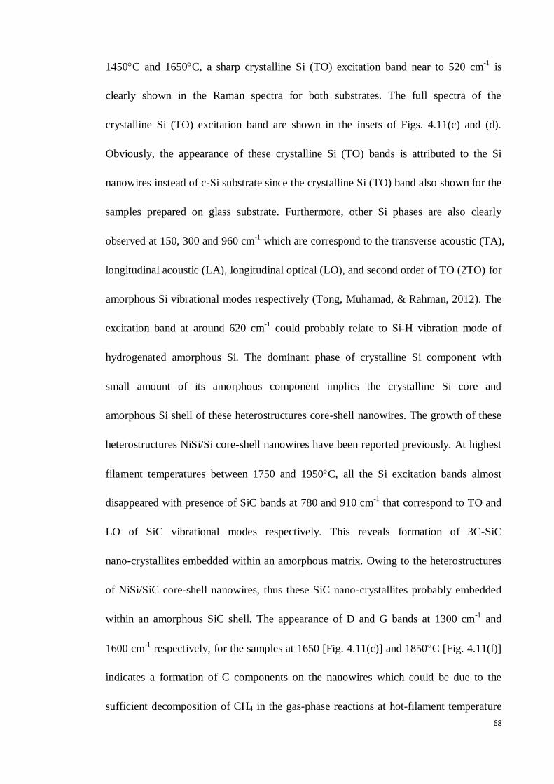
68
1450C and 1650C, a sharp crystalline Si (TO) excitation band near to 520 cm-1
is
clearly shown in the Raman spectra for both substrates. The full spectra of the
crystalline Si (TO) excitation band are shown in the insets of Figs. 4.11(c) and (d).
Obviously, the appearance of these crystalline Si (TO) bands is attributed to the Si
nanowires instead of c-Si substrate since the crystalline Si (TO) band also shown for the
samples prepared on glass substrate. Furthermore, other Si phases are also clearly
observed at 150, 300 and 960 cm-1
which are correspond to the transverse acoustic (TA),
longitudinal acoustic (LA), longitudinal optical (LO), and second order of TO (2TO) for
amorphous Si vibrational modes respectively (Tong, Muhamad, & Rahman, 2012). The
excitation band at around 620 cm-1
could probably relate to Si-H vibration mode of
hydrogenated amorphous Si. The dominant phase of crystalline Si component with
small amount of its amorphous component implies the crystalline Si core and
amorphous Si shell of these heterostructures core-shell nanowires. The growth of these
heterostructures NiSi/Si core-shell nanowires have been reported previously. At highest
filament temperatures between 1750 and 1950C, all the Si excitation bands almost
disappeared with presence of SiC bands at 780 and 910 cm-1
that correspond to TO and
LO of SiC vibrational modes respectively. This reveals formation of 3C-SiC
nano-crystallites embedded within an amorphous matrix. Owing to the heterostructures
of NiSi/SiC core-shell nanowires, thus these SiC nano-crystallites probably embedded
within an amorphous SiC shell. The appearance of D and G bands at 1300 cm-1
and
1600 cm-1
respectively, for the samples at 1650 [Fig. 4.11(c)] and 1850C [Fig. 4.11(f)]
indicates a formation of C components on the nanowires which could be due to the
sufficient decomposition of CH4 in the gas-phase reactions at hot-filament temperature
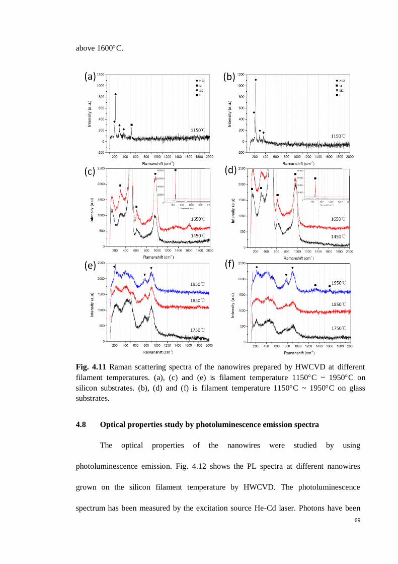
69
above 1600C.
Fig. 4.11 Raman scattering spectra of the nanowires prepared by HWCVD at different
filament temperatures. (a), (c) and (e) is filament temperature 1150C ~ 1950C on
silicon substrates. (b), (d) and (f) is filament temperature 1150C ~ 1950C on glass
substrates.
4.8 Optical properties study by photoluminescence emission spectra
The optical properties of the nanowires were studied by using
photoluminescence emission. Fig. 4.12 shows the PL spectra at different nanowires
grown on the silicon filament temperature by HWCVD. The photoluminescence
spectrum has been measured by the excitation source He-Cd laser. Photons have been
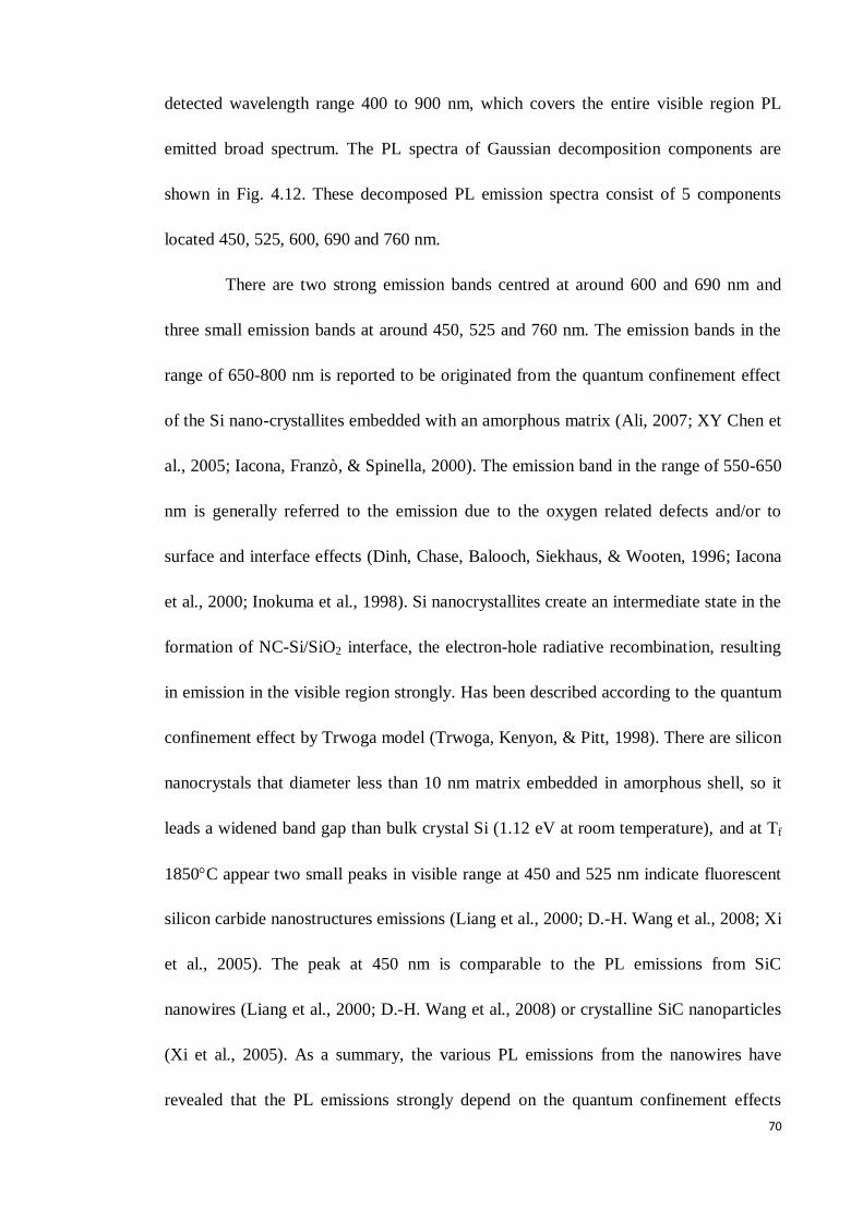
70
detected wavelength range 400 to 900 nm, which covers the entire visible region PL
emitted broad spectrum. The PL spectra of Gaussian decomposition components are
shown in Fig. 4.12. These decomposed PL emission spectra consist of 5 components
located 450, 525, 600, 690 and 760 nm.
There are two strong emission bands centred at around 600 and 690 nm and
three small emission bands at around 450, 525 and 760 nm. The emission bands in the
range of 650-800 nm is reported to be originated from the quantum confinement effect
of the Si nano-crystallites embedded with an amorphous matrix (Ali, 2007; XY Chen et
al., 2005; Iacona, Franzò, & Spinella, 2000). The emission band in the range of 550-650
nm is generally referred to the emission due to the oxygen related defects and/or to
surface and interface effects (Dinh, Chase, Balooch, Siekhaus, & Wooten, 1996; Iacona
et al., 2000; Inokuma et al., 1998). Si nanocrystallites create an intermediate state in the
formation of NC-Si/SiO2 interface, the electron-hole radiative recombination, resulting
in emission in the visible region strongly. Has been described according to the quantum
confinement effect by Trwoga model (Trwoga, Kenyon, & Pitt, 1998). There are silicon
nanocrystals that diameter less than 10 nm matrix embedded in amorphous shell, so it
leads a widened band gap than bulk crystal Si (1.12 eV at room temperature), and at Tf
1850C appear two small peaks in visible range at 450 and 525 nm indicate fluorescent
silicon carbide nanostructures emissions (Liang et al., 2000; D.-H. Wang et al., 2008; Xi
et al., 2005). The peak at 450 nm is comparable to the PL emissions from SiC
nanowires (Liang et al., 2000; D.-H. Wang et al., 2008) or crystalline SiC nanoparticles
(Xi et al., 2005). As a summary, the various PL emissions from the nanowires have
revealed that the PL emissions strongly depend on the quantum confinement effects
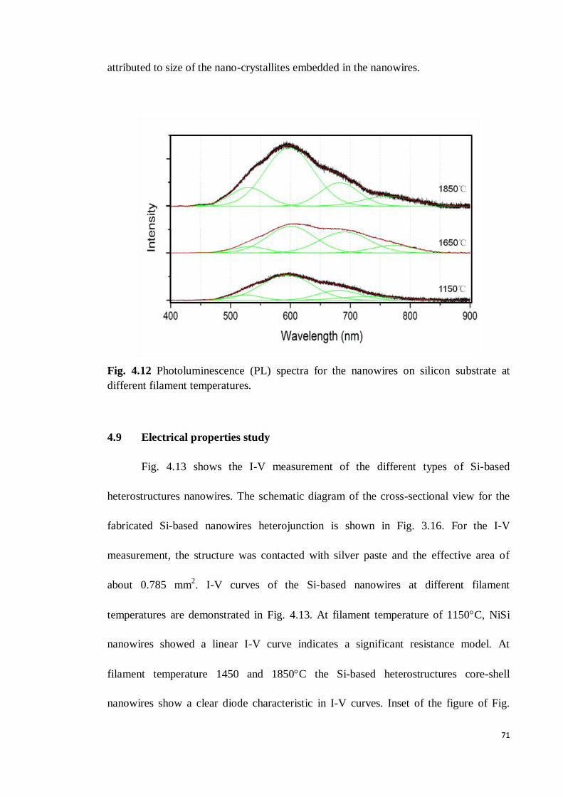
71
attributed to size of the nano-crystallites embedded in the nanowires.
Fig. 4.12 Photoluminescence (PL) spectra for the nanowires on silicon substrate at
different filament temperatures.
4.9 Electrical properties study
Fig. 4.13 shows the I-V measurement of the different types of Si-based
heterostructures nanowires. The schematic diagram of the cross-sectional view for the
fabricated Si-based nanowires heterojunction is shown in Fig. 3.16. For the I-V
measurement, the structure was contacted with silver paste and the effective area of
about 0.785 mm2. I-V curves of the Si-based nanowires at different filament
temperatures are demonstrated in Fig. 4.13. At filament temperature of 1150C, NiSi
nanowires showed a linear I-V curve indicates a significant resistance model. At
filament temperature 1450 and 1850C the Si-based heterostructures core-shell
nanowires show a clear diode characteristic in I-V curves. Inset of the figure of Fig.
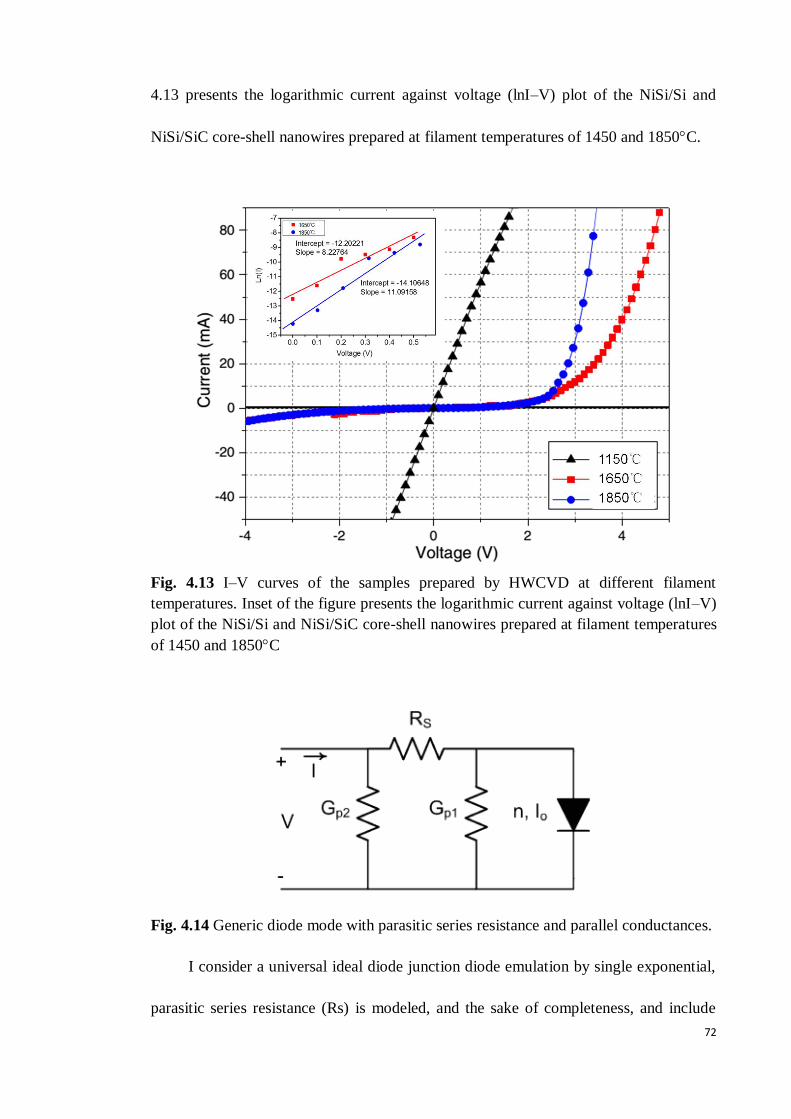
72
4.13 presents the logarithmic current against voltage (lnI–V) plot of the NiSi/Si and
NiSi/SiC core-shell nanowires prepared at filament temperatures of 1450 and 1850C.
Fig. 4.13 I–V curves of the samples prepared by HWCVD at different filament
temperatures. Inset of the figure presents the logarithmic current against voltage (lnI–V)
plot of the NiSi/Si and NiSi/SiC core-shell nanowires prepared at filament temperatures
of 1450 and 1850C
Fig. 4.14 Generic diode mode with parasitic series resistance and parallel conductances.
I consider a universal ideal diode junction diode emulation by single exponential,
parasitic series resistance (Rs) is modeled, and the sake of completeness, and include
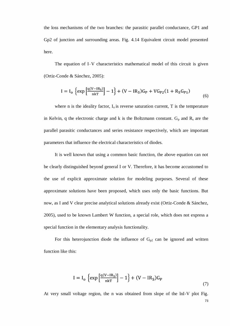
73
the loss mechanisms of the two branches: the parasitic parallel conductance, GP1 and
Gp2 of junction and surrounding areas. Fig. 4.14 Equivalent circuit model presented
here.
The equation of I–V characteristics mathematical model of this circuit is given
(Ortiz-Conde & Sánchez, 2005):
(6)
where n is the ideality factor, Io is reverse saturation current, T is the temperature
in Kelvin, q the electronic charge and k is the Boltzmann constant. Gp and Rs are the
parallel parasitic conductances and series resistance respectively, which are important
parameters that influence the electrical characteristics of diodes.
It is well known that using a common basic function, the above equation can not
be clearly distinguished beyond general I or V. Therefore, it has become accustomed to
the use of explicit approximate solution for modeling purposes. Several of these
approximate solutions have been proposed, which uses only the basic functions. But
now, as I and V clear precise analytical solutions already exist (Ortiz-Conde & Sánchez,
2005), used to be known Lambert W function, a special role, which does not express a
special function in the elementary analysis functionality.
For this heterojunction diode the influence of Gp2 can be ignored and written
function like this:
(7)
At very small voltage region, the n was obtained from slope of the lnI-V plot Fig.
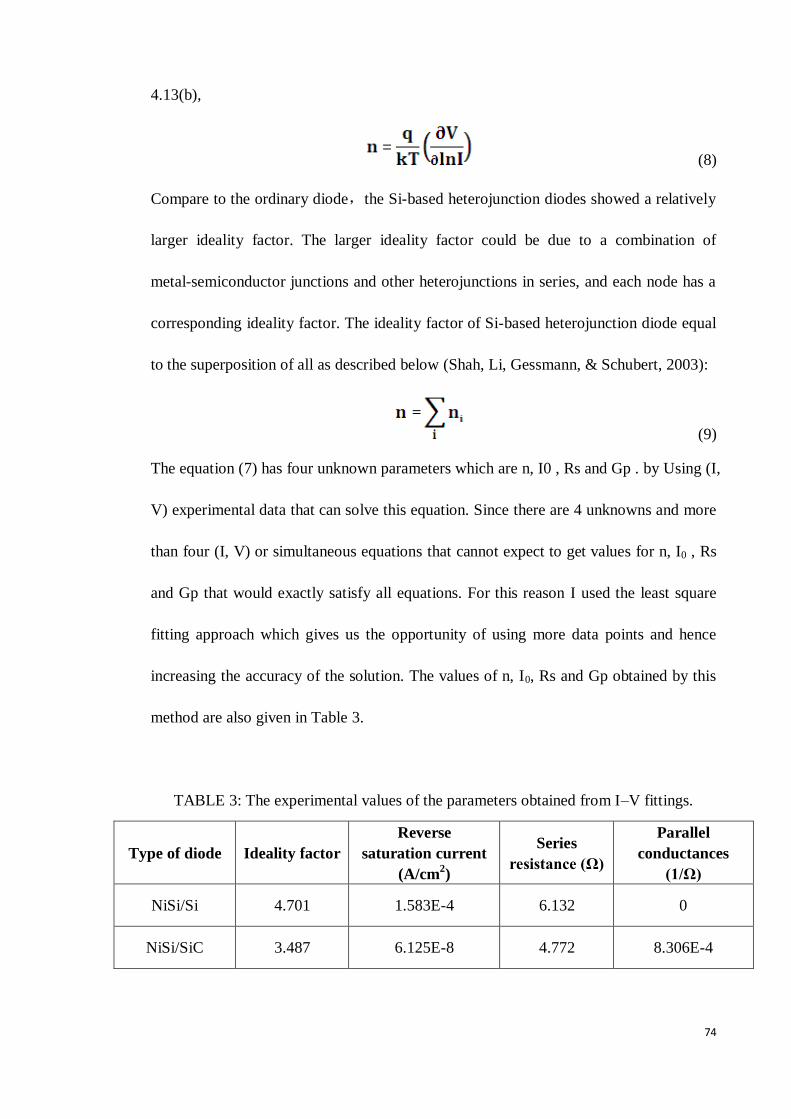
74
4.13(b),
(8)
Compare to the ordinary diode,the Si-based heterojunction diodes showed a relatively
larger ideality factor. The larger ideality factor could be due to a combination of
metal-semiconductor junctions and other heterojunctions in series, and each node has a
corresponding ideality factor. The ideality factor of Si-based heterojunction diode equal
to the superposition of all as described below (Shah, Li, Gessmann, & Schubert, 2003):
(9)
The equation (7) has four unknown parameters which are n, I0 , Rs and Gp . by Using (I,
V) experimental data that can solve this equation. Since there are 4 unknowns and more
than four (I, V) or simultaneous equations that cannot expect to get values for n, I0 , Rs
and Gp that would exactly satisfy all equations. For this reason I used the least square
fitting approach which gives us the opportunity of using more data points and hence
increasing the accuracy of the solution. The values of n, I0, Rs and Gp obtained by this
method are also given in Table 3.
TABLE 3: The experimental values of the parameters obtained from I–V fittings.
Type of diode Ideality factor
Reverse
saturation current
(A/cm2)
Series
resistance (Ω)
Parallel
conductances
(1/Ω)
NiSi/Si 4.701 1.583E-4 6.132 0
NiSi/SiC 3.487 6.125E-8 4.772 8.306E-4
75
CHAPTER 5
CONCLUSION
The growth, structural and electrical properties of the Ni-catalyzed Si-based
nanowires prepared by HWCVD at different filament temperatures has been
investigated. Different types of Si-based heterostructures nanowires have been
successfully grown by HWCVD at different filament temperatures. The structural and
electrical properties of the nanowires are presented.
The filament temperature played an important role in controlling the
decomposition mechanism, in which of the source gases and gas phase reactions thus
led to the growth of different types of the Si-based heterostructures nanowires. The
growth of NiSi nanowires at low filament temperature followed the solid phase
diffusion of the Si into Ni nanoparticles where the SiH4 was catalytically decomposed
by the Ni nanoparticles. Increase in the filament temperature involved the
decomposition of the source gases by hot-filament and promotes growth of he NiSi/Si
and NiSi/SiC heterostructures core-shell nanowires at 1450 and 1850C, respectively.
Formation of thin and long NiSi/SiC core-shell nanowires was attributed to the
diffusion of C-rich species formed SiC shell layer radially which limited the radial
growth of Si nanocolumns. Both NiSi/Si and NiSi/SiC heterostructures core-shell
nanowires exhibited heterojunction electrical characteristic which could be used for
nanoscale diode applications. Those properties prove that silicon based heterostructures
nanowires can be used for versatile sensor at harsh environment. Future work is in
progress to understand the correlation between work function and conductance results,

76
and how to assemble the nanowire device effectively is also need be studied.
77
REFERENCES
Ali, Atif Mossad. (2007). Origin of photoluminescence in nanocrystalline Si: H films.
Journal of luminescence, 126(2), 614-622.
Bae, Joonho, Kim, Hyunjin, Zhang, Xiao-Mei, Dang, Cuong H, Zhang, Yue, Choi,
Young Jin, . . . Wang, Zhong Lin. (2010). Si nanowire
metal–insulator–semiconductor photodetectors as efficient light harvesters.
Nanotechnology, 21(9), 095502.
Bandaru, PR, & Pichanusakorn, P. (2010). An outline of the synthesis and properties of
silicon nanowires. Semiconductor science and technology, 25(2), 024003.
Bhatnagar, Mohit, & Baliga, B Jayant. (1993). Comparison of 6H-SiC, 3C-SiC, and Si
for power devices. Electron Devices, IEEE Transactions on, 40(3), 645-655.
Bi, Jinghui, Wei, Guodong, Wang, Lin, Gao, Fengmei, Zheng, Jinju, Tang, Bin, & Yang,
Weiyou. (2013). Highly sensitive piezoresistance behaviors of n-type 3C-SiC
nanowires. J. Mater. Chem. C, 1(30), 4514-4517.
Borowiak-Palen, E, Ruemmeli, MH, Gemming, T, Knupfer, M, Biedermann, K,
Leonhardt, A, . . . Kalenczuk, RJ. (2005). Bulk synthesis of carbon-filled silicon
carbide nanotubes with a narrow diameter distribution. Journal of applied
physics, 97(5), 056102.
Casady, JB, & Johnson, R Wayne. (1996). Status of silicon carbide (SiC) as a
wide-bandgap semiconductor for high-temperature applications: A review.
Solid-State Electronics, 39(10), 1409-1422.
Characterization Techniques for Nanomaterials. (2008) Nanotechnology-Enabled
Sensors: Springer US.
Chen, Xihong, Xing, Yingjie, Xu, Jun, Xiang, Jie, & Yu, Dapeng. (2003). Rational
growth of highly oriented amorphous silicon nanowire films. Chemical physics
letters, 374(5), 626-630.
Chen, XY, Lu, YF, Tang, LJ, Wu, YH, Cho, BJ, Xu, XJ, . . . Song, WD. (2005).
Annealing and oxidation of silicon oxide films prepared by plasma-enhanced
chemical vapor deposition. Journal of Applied Physics, 97(1), 014913.
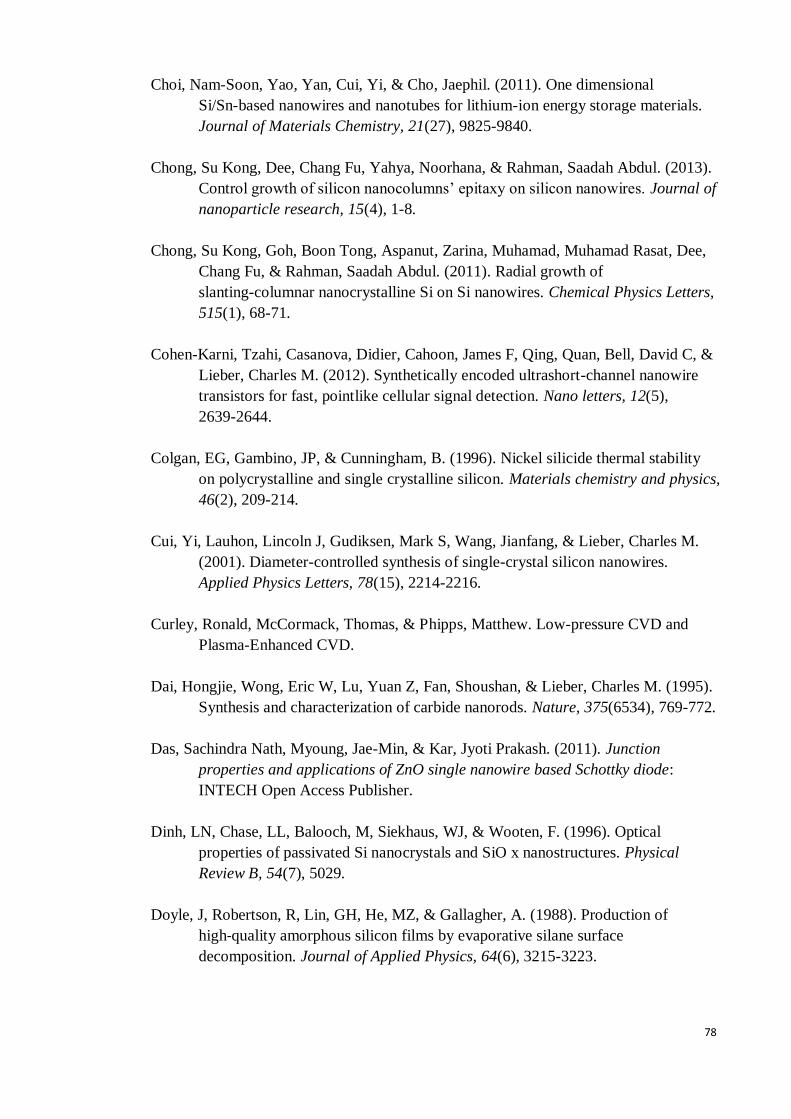
78
Choi, Nam-Soon, Yao, Yan, Cui, Yi, & Cho, Jaephil. (2011). One dimensional
Si/Sn-based nanowires and nanotubes for lithium-ion energy storage materials.
Journal of Materials Chemistry, 21(27), 9825-9840.
Chong, Su Kong, Dee, Chang Fu, Yahya, Noorhana, & Rahman, Saadah Abdul. (2013).
Control growth of silicon nanocolumns’ epitaxy on silicon nanowires. Journal of
nanoparticle research, 15(4), 1-8.
Chong, Su Kong, Goh, Boon Tong, Aspanut, Zarina, Muhamad, Muhamad Rasat, Dee,
Chang Fu, & Rahman, Saadah Abdul. (2011). Radial growth of
slanting-columnar nanocrystalline Si on Si nanowires. Chemical Physics Letters,
515(1), 68-71.
Cohen-Karni, Tzahi, Casanova, Didier, Cahoon, James F, Qing, Quan, Bell, David C, &
Lieber, Charles M. (2012). Synthetically encoded ultrashort-channel nanowire
transistors for fast, pointlike cellular signal detection. Nano letters, 12(5),
2639-2644.
Colgan, EG, Gambino, JP, & Cunningham, B. (1996). Nickel silicide thermal stability
on polycrystalline and single crystalline silicon. Materials chemistry and physics,
46(2), 209-214.
Cui, Yi, Lauhon, Lincoln J, Gudiksen, Mark S, Wang, Jianfang, & Lieber, Charles M.
(2001). Diameter-controlled synthesis of single-crystal silicon nanowires.
Applied Physics Letters, 78(15), 2214-2216.
Curley, Ronald, McCormack, Thomas, & Phipps, Matthew. Low-pressure CVD and
Plasma-Enhanced CVD.
Dai, Hongjie, Wong, Eric W, Lu, Yuan Z, Fan, Shoushan, & Lieber, Charles M. (1995).
Synthesis and characterization of carbide nanorods. Nature, 375(6534), 769-772.
Das, Sachindra Nath, Myoung, Jae-Min, & Kar, Jyoti Prakash. (2011). Junction
properties and applications of ZnO single nanowire based Schottky diode:
INTECH Open Access Publisher.
Dinh, LN, Chase, LL, Balooch, M, Siekhaus, WJ, & Wooten, F. (1996). Optical
properties of passivated Si nanocrystals and SiO x nanostructures. Physical
Review B, 54(7), 5029.
Doyle, J, Robertson, R, Lin, GH, He, MZ, & Gallagher, A. (1988). Production of
high‐quality amorphous silicon films by evaporative silane surface
decomposition. Journal of Applied Physics, 64(6), 3215-3223.
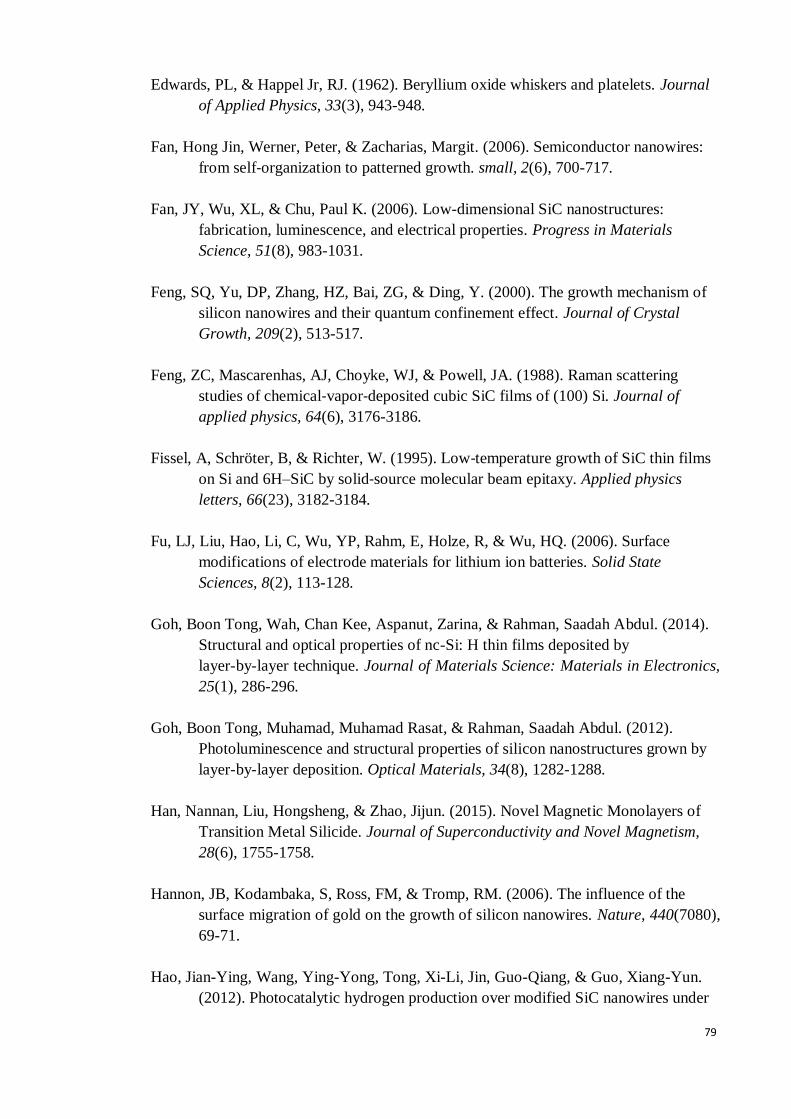
79
Edwards, PL, & Happel Jr, RJ. (1962). Beryllium oxide whiskers and platelets. Journal
of Applied Physics, 33(3), 943-948.
Fan, Hong Jin, Werner, Peter, & Zacharias, Margit. (2006). Semiconductor nanowires:
from self‐organization to patterned growth. small, 2(6), 700-717.
Fan, JY, Wu, XL, & Chu, Paul K. (2006). Low-dimensional SiC nanostructures:
fabrication, luminescence, and electrical properties. Progress in Materials
Science, 51(8), 983-1031.
Feng, SQ, Yu, DP, Zhang, HZ, Bai, ZG, & Ding, Y. (2000). The growth mechanism of
silicon nanowires and their quantum confinement effect. Journal of Crystal
Growth, 209(2), 513-517.
Feng, ZC, Mascarenhas, AJ, Choyke, WJ, & Powell, JA. (1988). Raman scattering
studies of chemical‐vapor‐deposited cubic SiC films of (100) Si. Journal of
applied physics, 64(6), 3176-3186.
Fissel, A, Schröter, B, & Richter, W. (1995). Low‐temperature growth of SiC thin films
on Si and 6H–SiC by solid‐source molecular beam epitaxy. Applied physics
letters, 66(23), 3182-3184.
Fu, LJ, Liu, Hao, Li, C, Wu, YP, Rahm, E, Holze, R, & Wu, HQ. (2006). Surface
modifications of electrode materials for lithium ion batteries. Solid State
Sciences, 8(2), 113-128.
Goh, Boon Tong, Wah, Chan Kee, Aspanut, Zarina, & Rahman, Saadah Abdul. (2014).
Structural and optical properties of nc-Si: H thin films deposited by
layer-by-layer technique. Journal of Materials Science: Materials in Electronics,
25(1), 286-296.
Goh, Boon Tong, Muhamad, Muhamad Rasat, & Rahman, Saadah Abdul. (2012).
Photoluminescence and structural properties of silicon nanostructures grown by
layer-by-layer deposition. Optical Materials, 34(8), 1282-1288.
Han, Nannan, Liu, Hongsheng, & Zhao, Jijun. (2015). Novel Magnetic Monolayers of
Transition Metal Silicide. Journal of Superconductivity and Novel Magnetism,
28(6), 1755-1758.
Hannon, JB, Kodambaka, S, Ross, FM, & Tromp, RM. (2006). The influence of the
surface migration of gold on the growth of silicon nanowires. Nature, 440(7080),
69-71.
Hao, Jian-Ying, Wang, Ying-Yong, Tong, Xi-Li, Jin, Guo-Qiang, & Guo, Xiang-Yun.
(2012). Photocatalytic hydrogen production over modified SiC nanowires under
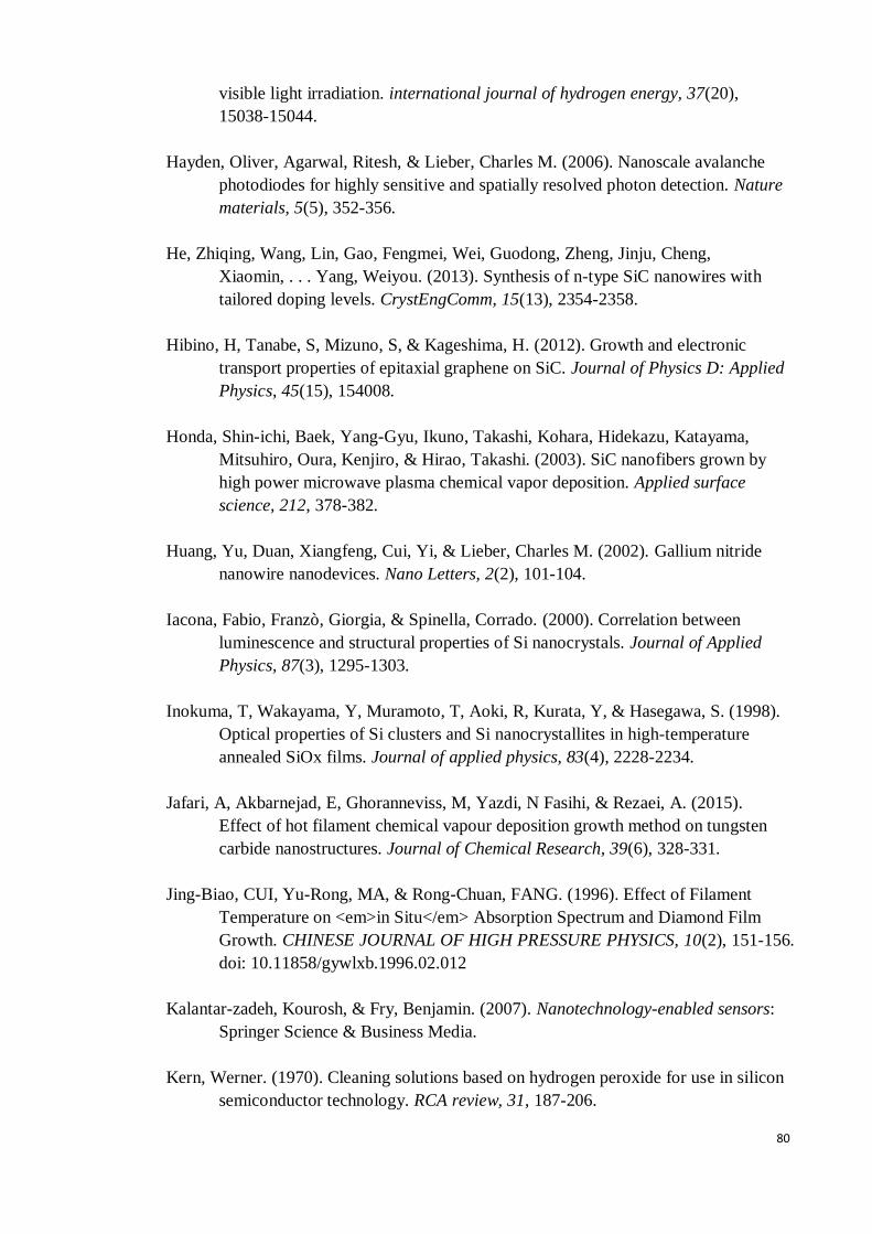
80
visible light irradiation. international journal of hydrogen energy, 37(20),
15038-15044.
Hayden, Oliver, Agarwal, Ritesh, & Lieber, Charles M. (2006). Nanoscale avalanche
photodiodes for highly sensitive and spatially resolved photon detection. Nature
materials, 5(5), 352-356.
He, Zhiqing, Wang, Lin, Gao, Fengmei, Wei, Guodong, Zheng, Jinju, Cheng,
Xiaomin, . . . Yang, Weiyou. (2013). Synthesis of n-type SiC nanowires with
tailored doping levels. CrystEngComm, 15(13), 2354-2358.
Hibino, H, Tanabe, S, Mizuno, S, & Kageshima, H. (2012). Growth and electronic
transport properties of epitaxial graphene on SiC. Journal of Physics D: Applied
Physics, 45(15), 154008.
Honda, Shin-ichi, Baek, Yang-Gyu, Ikuno, Takashi, Kohara, Hidekazu, Katayama,
Mitsuhiro, Oura, Kenjiro, & Hirao, Takashi. (2003). SiC nanofibers grown by
high power microwave plasma chemical vapor deposition. Applied surface
science, 212, 378-382.
Huang, Yu, Duan, Xiangfeng, Cui, Yi, & Lieber, Charles M. (2002). Gallium nitride
nanowire nanodevices. Nano Letters, 2(2), 101-104.
Iacona, Fabio, Franzò, Giorgia, & Spinella, Corrado. (2000). Correlation between
luminescence and structural properties of Si nanocrystals. Journal of Applied
Physics, 87(3), 1295-1303.
Inokuma, T, Wakayama, Y, Muramoto, T, Aoki, R, Kurata, Y, & Hasegawa, S. (1998).
Optical properties of Si clusters and Si nanocrystallites in high-temperature
annealed SiOx films. Journal of applied physics, 83(4), 2228-2234.
Jafari, A, Akbarnejad, E, Ghoranneviss, M, Yazdi, N Fasihi, & Rezaei, A. (2015).
Effect of hot filament chemical vapour deposition growth method on tungsten
carbide nanostructures. Journal of Chemical Research, 39(6), 328-331.
Jing-Biao, CUI, Yu-Rong, MA, & Rong-Chuan, FANG. (1996). Effect of Filament
Temperature on <em>in Situ</em> Absorption Spectrum and Diamond Film
Growth. CHINESE JOURNAL OF HIGH PRESSURE PHYSICS, 10(2), 151-156.
doi: 10.11858/gywlxb.1996.02.012
Kalantar-zadeh, Kourosh, & Fry, Benjamin. (2007). Nanotechnology-enabled sensors:
Springer Science & Business Media.
Kern, Werner. (1970). Cleaning solutions based on hydrogen peroxide for use in silicon
semiconductor technology. RCA review, 31, 187-206.
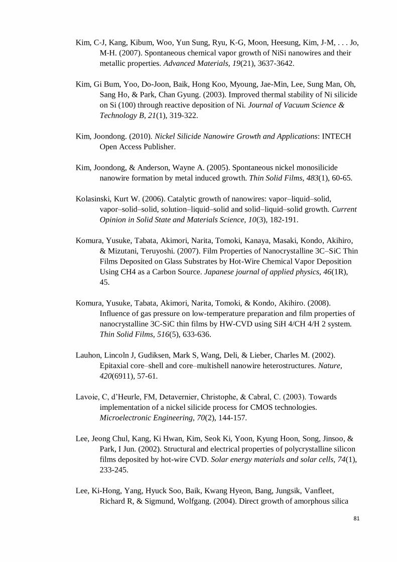
81
Kim, C‐J, Kang, Kibum, Woo, Yun Sung, Ryu, K‐G, Moon, Heesung, Kim, J‐M, . . . Jo,
M‐H. (2007). Spontaneous chemical vapor growth of NiSi nanowires and their
metallic properties. Advanced Materials, 19(21), 3637-3642.
Kim, Gi Bum, Yoo, Do-Joon, Baik, Hong Koo, Myoung, Jae-Min, Lee, Sung Man, Oh,
Sang Ho, & Park, Chan Gyung. (2003). Improved thermal stability of Ni silicide
on Si (100) through reactive deposition of Ni. Journal of Vacuum Science &
Technology B, 21(1), 319-322.
Kim, Joondong. (2010). Nickel Silicide Nanowire Growth and Applications: INTECH
Open Access Publisher.
Kim, Joondong, & Anderson, Wayne A. (2005). Spontaneous nickel monosilicide
nanowire formation by metal induced growth. Thin Solid Films, 483(1), 60-65.
Kolasinski, Kurt W. (2006). Catalytic growth of nanowires: vapor–liquid–solid,
vapor–solid–solid, solution–liquid–solid and solid–liquid–solid growth. Current
Opinion in Solid State and Materials Science, 10(3), 182-191.
Komura, Yusuke, Tabata, Akimori, Narita, Tomoki, Kanaya, Masaki, Kondo, Akihiro,
& Mizutani, Teruyoshi. (2007). Film Properties of Nanocrystalline 3C–SiC Thin
Films Deposited on Glass Substrates by Hot-Wire Chemical Vapor Deposition
Using CH4 as a Carbon Source. Japanese journal of applied physics, 46(1R),
45.
Komura, Yusuke, Tabata, Akimori, Narita, Tomoki, & Kondo, Akihiro. (2008).
Influence of gas pressure on low-temperature preparation and film properties of
nanocrystalline 3C-SiC thin films by HW-CVD using SiH 4/CH 4/H 2 system.
Thin Solid Films, 516(5), 633-636.
Lauhon, Lincoln J, Gudiksen, Mark S, Wang, Deli, & Lieber, Charles M. (2002).
Epitaxial core–shell and core–multishell nanowire heterostructures. Nature,
420(6911), 57-61.
Lavoie, C, d’Heurle, FM, Detavernier, Christophe, & Cabral, C. (2003). Towards
implementation of a nickel silicide process for CMOS technologies.
Microelectronic Engineering, 70(2), 144-157.
Lee, Jeong Chul, Kang, Ki Hwan, Kim, Seok Ki, Yoon, Kyung Hoon, Song, Jinsoo, &
Park, I Jun. (2002). Structural and electrical properties of polycrystalline silicon
films deposited by hot-wire CVD. Solar energy materials and solar cells, 74(1),
233-245.
Lee, Ki-Hong, Yang, Hyuck Soo, Baik, Kwang Hyeon, Bang, Jungsik, Vanfleet,
Richard R, & Sigmund, Wolfgang. (2004). Direct growth of amorphous silica
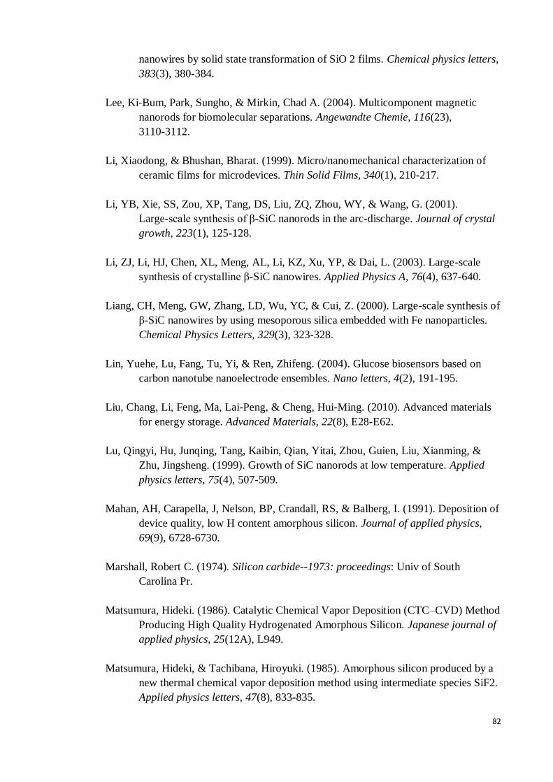
82
nanowires by solid state transformation of SiO 2 films. Chemical physics letters,
383(3), 380-384.
Lee, Ki‐Bum, Park, Sungho, & Mirkin, Chad A. (2004). Multicomponent magnetic
nanorods for biomolecular separations. Angewandte Chemie, 116(23),
3110-3112.
Li, Xiaodong, & Bhushan, Bharat. (1999). Micro/nanomechanical characterization of
ceramic films for microdevices. Thin Solid Films, 340(1), 210-217.
Li, YB, Xie, SS, Zou, XP, Tang, DS, Liu, ZQ, Zhou, WY, & Wang, G. (2001).
Large-scale synthesis of β-SiC nanorods in the arc-discharge. Journal of crystal
growth, 223(1), 125-128.
Li, ZJ, Li, HJ, Chen, XL, Meng, AL, Li, KZ, Xu, YP, & Dai, L. (2003). Large-scale
synthesis of crystalline β-SiC nanowires. Applied Physics A, 76(4), 637-640.
Liang, CH, Meng, GW, Zhang, LD, Wu, YC, & Cui, Z. (2000). Large-scale synthesis of
β-SiC nanowires by using mesoporous silica embedded with Fe nanoparticles.
Chemical Physics Letters, 329(3), 323-328.
Lin, Yuehe, Lu, Fang, Tu, Yi, & Ren, Zhifeng. (2004). Glucose biosensors based on
carbon nanotube nanoelectrode ensembles. Nano letters, 4(2), 191-195.
Liu, Chang, Li, Feng, Ma, Lai‐Peng, & Cheng, Hui‐Ming. (2010). Advanced materials
for energy storage. Advanced Materials, 22(8), E28-E62.
Lu, Qingyi, Hu, Junqing, Tang, Kaibin, Qian, Yitai, Zhou, Guien, Liu, Xianming, &
Zhu, Jingsheng. (1999). Growth of SiC nanorods at low temperature. Applied
physics letters, 75(4), 507-509.
Mahan, AH, Carapella, J, Nelson, BP, Crandall, RS, & Balberg, I. (1991). Deposition of
device quality, low H content amorphous silicon. Journal of applied physics,
69(9), 6728-6730.
Marshall, Robert C. (1974). Silicon carbide--1973: proceedings: Univ of South
Carolina Pr.
Matsumura, Hideki. (1986). Catalytic Chemical Vapor Deposition (CTC–CVD) Method
Producing High Quality Hydrogenated Amorphous Silicon. Japanese journal of
applied physics, 25(12A), L949.
Matsumura, Hideki, & Tachibana, Hiroyuki. (1985). Amorphous silicon produced by a
new thermal chemical vapor deposition method using intermediate species SiF2.
Applied physics letters, 47(8), 833-835.
83
Matthews, JW, & Blakeslee, AE. (1974). Defects in epitaxial multilayers: I. Misfit
dislocations. Journal of Crystal Growth, 27, 118-125.
McAlpine, Michael C, Ahmad, Habib, Wang, Dunwei, & Heath, James R. (2007).
Highly ordered nanowire arrays on plastic substrates for ultrasensitive flexible
chemical sensors. Nature materials, 6(5), 379-384.
Mehregany, M, Zorman, CA, Roy, S, Fleischman, AJ, & Rajan, N. (2000). Silicon
carbide for microelectromechanical systems. International materials reviews,
45(3), 85-108.
Mieszawska, Aneta J, Jalilian, Romaneh, Sumanasekera, Gamini U, & Zamborini,
Francis P. (2007). The Synthesis and Fabrication of One‐Dimensional Nanoscale
Heterojunctions. Small, 3(5), 722-756.
Morales, Alfredo M, & Lieber, Charles M. (1998). A laser ablation method for the
synthesis of crystalline semiconductor nanowires. Science, 279(5348), 208-211.
Ortiz-Conde, Adelmo, & Sánchez, Francisco J García. (2005). Extraction of non-ideal
junction model parameters from the explicit analytic solutions of its I–V
characteristics. Solid-state electronics, 49(3), 465-472.
Pallecchi, E, Lafont, F, Cavaliere, V, Schopfer, F, Mailly, D, Poirier, W, & Ouerghi, A.
(2014). High electron mobility in epitaxial graphene on 4H-SiC (0001) via
post-growth annealing under hydrogen. Scientific reports, 4.
Penn, Sharron G, He, Lin, & Natan, Michael J. (2003). Nanoparticles for bioanalysis.
Current opinion in chemical biology, 7(5), 609-615.
QI, Xue-Gui, CHANG, Chao, CHEN, Ze-Shao, WANG, Guan-Zhong, & LIAO, Yuan.
(2003). Simulation and Analysis of Gas Phase Environment in HFCVD
Diamond Films Growth. Journal of Inorganic Materials, 1, 031.
Rao, CNR, Deepak, F Leonard, Gundiah, Gautam, & Govindaraj, Achutharao. (2003).
Inorganic nanowires. Progress in Solid State Chemistry, 31(1), 5-147.
Robertson, R, Hils, D, & Gallagher, A. (1984). Silane pyrolysis. Chemical physics
letters, 103(5), 397-404.
Robertson, Robert, & Gallagher, Alan. (1986). Reaction mechanism and kinetics of
silane pyrolysis on a hydrogenated amorphous silicon surface. The Journal of
chemical physics, 85(6), 3623-3630.
Rurali, Riccardo. (2010). Colloquium: Structural, electronic, and transport properties of
silicon nanowires. Reviews of Modern Physics, 82(1), 427.
84
Salem, Aliasger K, Searson, Peter C, & Leong, Kam W. (2003). Multifunctional
nanorods for gene delivery. Nature materials, 2(10), 668-671.
Sarro, Pasqualina M. (2000). Silicon carbide as a new MEMS technology. Sensors and
Actuators A: Physical, 82(1), 210-218.
Schmidt, V, Wittemann, JV, & Gosele, U. (2010). Growth, thermodynamics, and
electrical properties of silicon nanowires†. Chemical reviews, 110(1), 361-388.
Schmidt, V., Wittemann, J. V., & Gösele, U. (2010). Growth, Thermodynamics, and
Electrical Properties of Silicon Nanowires. Chemical Reviews, 110(1), 361-388.
doi: 10.1021/cr900141g
Shah, Jay M, Li, Y-L, Gessmann, Th, & Schubert, EF. (2003). Experimental analysis
and theoretical model for anomalously high ideality factors (n≫ 2.0) in
AlGaN/GaN pn junction diodes. Journal of applied physics, 94(4), 2627-2630.
Suzuki, Hiroshi, Araki, Hiroshi, Tosa, Masahiro, & Noda, Tetsuji. (2007). Formation of
silicon nanowires by CVD using gold catalysts at low temperatures. Materials
transactions, 48(8), 2202-2206.
Tabata, Akimori, & Komura, Yusuke. (2007). Preparation of nanocrystalline cubic
silicon carbide thin films by hot-wire CVD at various filament-to-substrate
distances. Surface and Coatings Technology, 201(22), 8986-8990.
Tange, Shinya, Inoue, Keisuke, Tonokura, Kenichi, & Koshi, Mitsuo. (2001). Catalytic
decomposition of SiH 4 on a hot filament. Thin Solid Films, 395(1), 42-46.
Trwoga, PF, Kenyon, AJ, & Pitt, CW. (1998). Modeling the contribution of quantum
confinement to luminescence from silicon nanoclusters. Journal of applied
physics, 83(7), 3789-3794.
Wagner, RS, & Ellis, WC. (1964). Vapor‐liquid‐solid mechanism of single crystal
growth. Applied Physics Letters, 89-90.
Wan, Y, Sha, J, Chen, B, Fang, Y, Wang, Z, & Wang, Y. (2009). Recent Pat:
Nanotechnol.
Wang, Bing, Wang, Yingde, Lei, Yongpeng, Wu, Nan, Gou, Yanzi, Han, Cheng, &
Fang, Dong. (2014). Hierarchically porous SiC ultrathin fibers mat with
enhanced mass transport, amphipathic property and high-temperature erosion
resistance. Journal of Materials Chemistry A, 2(48), 20873-20881.
85
Wang, Dong-Hua, Xu, Di, Wang, Qing, Hao, Ya-Juan, Jin, Guo-Qiang, Guo,
Xiang-Yun, & Tu, KN. (2008). Periodically twinned SiC nanowires.
Nanotechnology, 19(21), 215602.
Wang, N, Tang, YH, Zhang, YF, Lee, CS, Bello, I, & Lee, ST. (1999). Si nanowires
grown from silicon oxide. Chemical physics letters, 299(2), 237-242.
Westwater, John, Gosain, DP, Tomiya, S, Usui, S, & Ruda, H. (1997). Growth of
silicon nanowires via gold/silane vapor–liquid–solid reaction. Journal of
Vacuum Science & Technology B, 15(3), 554-557.
Wiesmann, H, Ghosh, AK, McMahon, T, & Strongin, Myron. (1979). a‐Si: H produced
by high‐temperature thermal decomposition of silane. Journal of Applied
Physics, 50(5), 3752-3754.
Willander, Magnus, Friesel, Milan, Wahab, Qamar-ul, & Straumal, Boris. (2006).
Silicon carbide and diamond for high temperature device applications. Journal
of Materials Science: Materials in Electronics, 17(1), 1-25.
Wong, Eric W, Sheehan, Paul E, & Lieber, Charles M. (1997). Nanobeam mechanics:
elasticity, strength, and toughness of nanorods and nanotubes. Science,
277(5334), 1971-1975.
Wu, Yiying, & Yang, Peidong. (2001). Direct observation of vapor-liquid-solid
nanowire growth. Journal of the American Chemical Society, 123(13),
3165-3166.
Wu, Yue, Cui, Yi, Huynh, Lynn, Barrelet, Carl J, Bell, David C, & Lieber, Charles M.
(2004). Controlled growth and structures of molecular-scale silicon nanowires.
Nano Letters, 4(3), 433-436.
Wu, Yue, Xiang, Jie, Yang, Chen, Lu, Wei, & Lieber, Charles M. (2004). Single-crystal
metallic nanowires and metal/semiconductor nanowire heterostructures. Nature,
430(6995), 61-65.
Xi, Guangcheng, Yu, Shijun, Zhang, Rui, Zhang, Meng, Ma, Dekun, & Qian, Yitai.
(2005). Crystalline silicon carbide nanoparticles encapsulated in branched
wavelike carbon nanotubes: synthesis and optical properties. The Journal of
Physical Chemistry B, 109(27), 13200-13204.
Xia, Younan, Yang, Peidong, Sun, Yugang, Wu, Yiying, Mayers, Brian, Gates,
Byron, . . . Yan, Haoquan. (2003). One-dimensional nanostructures: synthesis,
characterization, and applications. Advanced materials, 15(5), 353-389.
86
Xiang, Jie, Lu, Wei, Hu, Yongjie, Wu, Yue, Yan, Hao, & Lieber, Charles M. (2006).
Ge/Si nanowire heterostructures as high-performance field-effect transistors.
Nature, 441(7092), 489-493.
Yakimova, Rositsa, Petoral Jr, RM, Yazdi, GR, Vahlberg, Cecilia, Lloyd Spetz, Anita,
& Uvdal, Kajsa. (2007). REVIEW ARTICLE: Surface functionalization and
biomedical applications based on SiC. Journal of Physics D Applied Physics, 40,
6435-6442.
Yan, HF, Xing, YJ, Hang, QL, Yu, DP, Wang, YP, Xu, J, . . . Feng, SQ. (2000). Growth
of amorphous silicon nanowires via a solid–liquid–solid mechanism. Chemical
Physics Letters, 323(3), 224-228.
Yan, Ruoxue, Gargas, Daniel, & Yang, Peidong. (2009). Nanowire photonics. Nature
Photonics, 3(10), 569-576.
Yu, DP, Bai, ZG, Ding, Y, Hang, QL, Zhang, HZ, Wang, JJ, . . . Zhou, HT. (1998).
Nanoscale silicon wires synthesized using simple physical evaporation. Applied
Physics Letters, 72(26), 3458-3460.
Yu, Linwei, O’Donnell, Benedict, Alet, Pierre-Jean, Conesa-Boj, S, Peiro, F, Arbiol, J,
& i Cabarrocas, Pere Roca. (2009). Plasma-enhanced low temperature growth of
silicon nanowires and hierarchical structures by using tin and indium catalysts.
Nanotechnology, 20(22), 225604.
Zeng, XB, Xu, YY, Zhang, SB, Hu, ZH, Diao, HW, Wang, YQ, . . . Liao, XB. (2003).
Silicon nanowires grown on a pre-annealed Si substrate. Journal of crystal
growth, 247(1), 13-16.
Zhang, HZ, Yu, DP, Ding, Y, Bai, ZG, Hang, QL, & Feng, SQ. (1998). Dependence of
the silicon nanowire diameter on ambient pressure. Applied physics letters,
73(23), 3396-3398.
Zhang, Shu-Lin, Zhu, Bang-fen, Huang, Fuming, Yan, Yan, Shang, Er-yi, Fan,
Shoushan, & Han, Weigiang. (1999). Effect of defects on optical phonon Raman
spectra in SiC nanorods. Solid state communications, 111(11), 647-651.
Zhou, XT, Wang, N, Lai, HL, Peng, HY, Bello, I, Wong, NB, . . . Lee, ST. (1999).
β-SiC nanorods synthesized by hot filament chemical vapor deposition. Applied
physics letters, 74(26), 3942-3944.
Zou, Guifu, Dong, Chao, Xiong, Kan, Li, Hui, Jiang, Changlong, & Qian, Yitai. (2006).
Low-temperature solvothermal route to 2H-SiC nanoflakes. Applied physics
letters, 88(7), 1913.