structural analysis of self‐assembled monolayers on …etheses.bham.ac.uk/4681/1/gao13phd.pdf ·...
TRANSCRIPT
Structural analysis of self‐assembled monolayers on Au(111) and point
defects on HOPG by
Jianzhi Gao
A thesis submitted to
The University of Birmingham
for the degree of
DOCTOR OF PHILOSOPHY
School of Physics and Astronomy
The University of Birmingham
June 2013

University of Birmingham Research Archive
e-theses repository This unpublished thesis/dissertation is copyright of the author and/or third parties. The intellectual property rights of the author or third parties in respect of this work are as defined by The Copyright Designs and Patents Act 1988 or as modified by any successor legislation. Any use made of information contained in this thesis/dissertation must be in accordance with that legislation and must be properly acknowledged. Further distribution or reproduction in any format is prohibited without the permission of the copyright holder.
i
Abstract
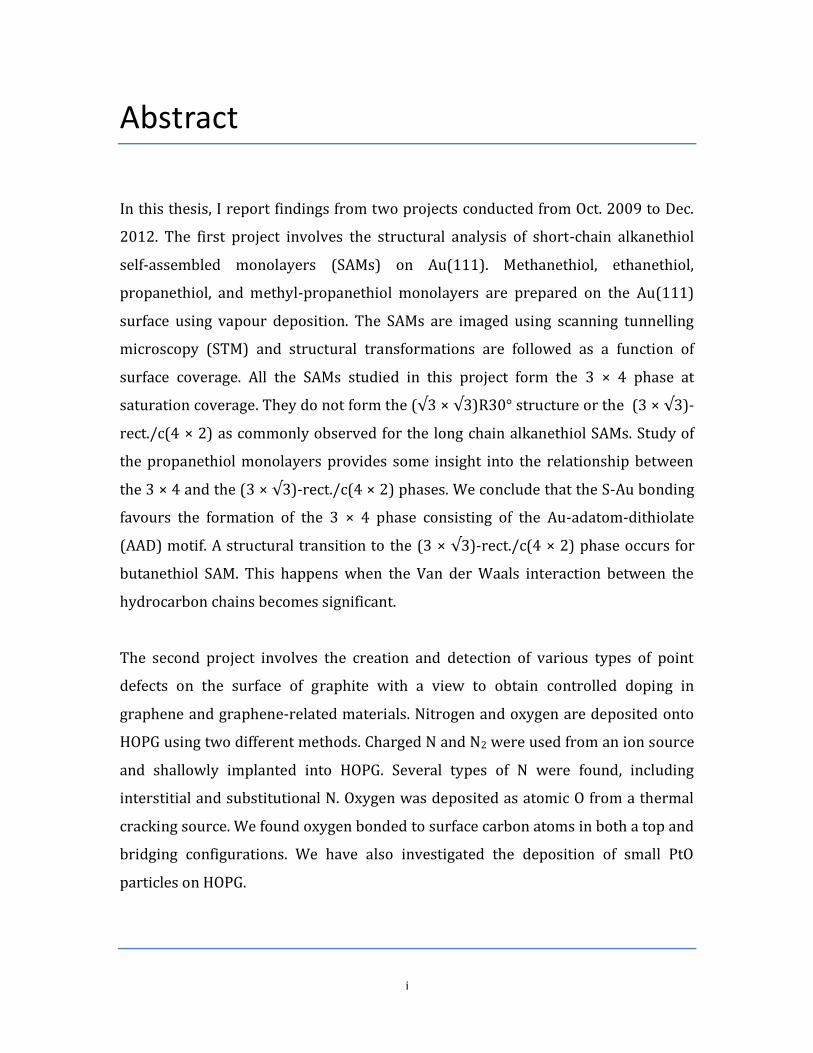
In this thesis, I report findings from two projects conducted from Oct. 2009 to Dec.
2012. The first project involves the structural analysis of short-chain alkanethiol
self-assembled monolayers (SAMs) on Au(111). Methanethiol, ethanethiol,
propanethiol, and methyl-propanethiol monolayers are prepared on the Au(111)
surface using vapour deposition. The SAMs are imaged using scanning tunnelling
microscopy (STM) and structural transformations are followed as a function of
surface coverage. All the SAMs studied in this project form the 3 × 4 phase at
saturation coverage. They do not form the (√3 × √3)R30° structure or the (3 × √3)-
rect./c(4 × 2) as commonly observed for the long chain alkanethiol SAMs. Study of
the propanethiol monolayers provides some insight into the relationship between
the 3 × 4 and the (3 × √3)-rect./c(4 × 2) phases. We conclude that the S-Au bonding
favours the formation of the 3 × 4 phase consisting of the Au-adatom-dithiolate
(AAD) motif. A structural transition to the (3 × √3)-rect./c(4 × 2) phase occurs for
butanethiol SAM. This happens when the Van der Waals interaction between the
hydrocarbon chains becomes significant.
The second project involves the creation and detection of various types of point
defects on the surface of graphite with a view to obtain controlled doping in
graphene and graphene-related materials. Nitrogen and oxygen are deposited onto
HOPG using two different methods. Charged N and N2 were used from an ion source
and shallowly implanted into HOPG. Several types of N were found, including
interstitial and substitutional N. Oxygen was deposited as atomic O from a thermal
cracking source. We found oxygen bonded to surface carbon atoms in both a top and
bridging configurations. We have also investigated the deposition of small PtO
particles on HOPG.

ii
Acknowledgements
Firstly, I would like to thank my supervisor Dr. Quanmin Guo. It was he who
introduced me to the scientific research, without whom the work presented in this
thesis would be impossible. I am indebted to him for his guidance and patient
throughout my PhD program. Secondly, I would like to express my appreciation to
Prof. Richard. E. Palmer, Dr Ziyou Li and Dr. Wolfgan Theis for thought-provoking
discussions and illuminating. I would also like to thank Dr Lin Tang, Dr Fangsen Li,
Dr Xin Zhang, Dr Feng Yin, Dr Thibault Decoster and Dr Tianluo Pan for the help
with the UHV system and STM. Furthermore, discussions with Lu Cao, Dongxu Yang,
Yangchun Xie, and Ray Hu throughout the doctoral program are highly valued and
appreciated. I recognize all the members who now work or used to work in the
NPRL for advice and friendship. Special thanks must go to my parents Xiurong Gao,
Binglin Gao, my yonger sister Jiantong Gao and my girl friend Kaixuan Gao, who
selflessly supported and encouraged me.
iii
Table of Contents
Chapter 1 Introduction ............................................................................................................................... 1 Chapter 2 Literature review..................................................................................................................... 6
2.1 Au (111) ........................................................................................................................................... 6 2.2 Self-assembled monolayer of alkanethiol molecules .............................................. 16
2.2.1 Preparation of alkanethiol self-assembled monolayers .......................... 18 2.2.2 Deposition process of alkanethiol molecules ................................................ 20 2.2.3 Structural properties of self-assembled monolayers of alkanethiol molecules on Au(111) .......................................................................................................... 25
2.3 Highly oriented pyrolytic graphite (HOPG) ................................................................. 43 2.3.1 Basic physical properties of HOPG ..................................................................... 44 2.3.2 Fundamental electronic properties ................................................................... 47 2.3.3 Point defects created by ion bombardment ................................................... 64
Chapter 3 Experimental techniques and methodology ........................................................... 70 3.1 Surface analysis methods ..................................................................................................... 70 3.2 Scanning Tunnelling Microscopy ...................................................................................... 72 3.3 VT-STM .......................................................................................................................................... 78 3.4 ISE 5 ion gun ............................................................................................................................... 84 3.5 Sample and tip preparation ................................................................................................. 85
Chapter 4 Adsorption of short chain alkanethiol molecules on Au(111) ....................... 93 4.1The structure of methylthiolate and ethylthiolate monolayers on Au(111). 94
4.1.1 Absence of the o phase-methylthiolate monolayer. .... 94
4.1.2 Absence of the 0 phase-ethylthiolate monolayer. ........ 98 4.2 The structure of propyl-thiolate monolayers on Au (111). ................................102
4.2.1 Short range ordered 3 4 phase-propylthiolate monolayer. ...............103 4.2.2 Adsorption of methyl-propyl disulfide on Au(111) .................................114 4.2.3 Propylthiolate striped phases .............................................................................120
Chapter 5 Low energy sputtering with argon and nitrogen on HOPG (0001) ............126 5.1 Low energy Argon ion bombardment of HOPG (0001) .......................................126 5.2 Low energy Nitrogen ion bombardment on HOPG (0001) ................................135
Chapter 6 Thermally cracked atomic oxygen on HOPG (0001) .........................................151 6.1 Pinning platinum and Pt-oxide nanoparticles on graphite ................................151 6.2 Binding of atomic oxygen to HOPG ................................................................................163
Chapter 7 Conclusion..............................................................................................................................181 References ...................................................................................................................................................183

iv
Abbreviations list
AAD: Au-adatom-dimethylthiolate. AFM: Atomic force microscopy. CFM: Chemical force microscopy. DFT: Density functional theory. DLs: Discommensuration lines. DMDS: Dimethyl disulfide. EFM: Electrostatic force microscopy. ET: Ethylthiolate. FCC: Face-centred cubic. FEL: Fast entry lock. FFT: Fast fourier transform. GIXD: Grazing incidence X-ray diffraction. HAS: Helium atom scattering. HCP: Hexagonal close-packed. HDRS: Hydrogen direct recoil spectroscopy. HOPG: Highly oriented pyrolytic graphite. IR: Infrared spectroscopy. KPFM: Kelvin probe force microscopy. LEAD: Low energy atom diffraction. LEED: Low energy electron diffraction. MFM: Magnetic force microscopy. MPDS: Methyl-propyl-disulfide. MPT: Methyl-propylthiolated. MT: Methylthiolate. PT: Propylthiolate. RHEED: Reflection high-energy electron diffraction. RT: Room temperature. SAM: Self-assembled monolayers. SCM: Scanning capacitance microscopy. SMSI: Strong-metal-support-interaction. SPM: Scanning probe microscopy. STM: Scanning tunneling microscopy. STS: Scanning tunnelling spectroscopy. TCPG: Thermal Conductive Pyrolytic Graphite. TEM: Transmission electron microscopy. TPD: Temperature-programmed desorption. UHV: Ultra High Vacuum. VT: Variable temperature. XPS: X-ray diffraction spectroscopy. 0D: 0 dimension 1D: 1 dimension. 2D: 2 dimension.
v
Publications
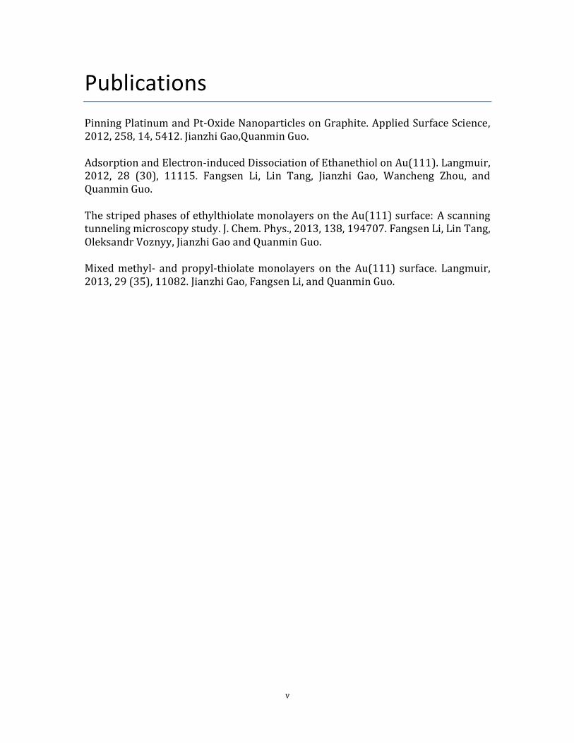
Pinning Platinum and Pt-Oxide Nanoparticles on Graphite. Applied Surface Science, 2012, 258, 14, 5412. Jianzhi Gao,Quanmin Guo. Adsorption and Electron-induced Dissociation of Ethanethiol on Au(111). Langmuir, 2012, 28 (30), 11115. Fangsen Li, Lin Tang, Jianzhi Gao, Wancheng Zhou, and Quanmin Guo. The striped phases of ethylthiolate monolayers on the Au(111) surface: A scanning tunneling microscopy study. J. Chem. Phys., 2013, 138, 194707. Fangsen Li, Lin Tang, Oleksandr Voznyy, Jianzhi Gao and Quanmin Guo. Mixed methyl- and propyl-thiolate monolayers on the Au(111) surface. Langmuir, 2013, 29 (35), 11082. Jianzhi Gao, Fangsen Li, and Quanmin Guo.
Jianzhi Gao’s PhD thesis
1
Chapter 1 Introduction
The development of nanoscale technology has significantly progressed and now
takes a serious place in the field of physics, chemistry and bioscience. It attracts the
attention of many scientists and has become a dominant research area for the 21st
century, with extremely high potential, in micro and nano-engineering and other
related areas. The general understanding of the concept of nanoscale
technology/science is focusing on the objects or phenomena at the scale of 1-100
nm. The objects can have many interesting and important properties at such a small
scale contributed by, for example the surface atoms of nanoscale objects. These
unique properties of the surfaces make the surface state the fourth physical state
after gas state, liquid state and solid state (note: there is also a well known state
plasma) [1].
Surface atoms or molecules have different mobility, structure, energy state, and
reactivity from those in the bulk [2,3]. For example, graphene [4] is a 2D material,
which is composed of surface atoms only and has many interesting properties. (The
details of graphene will be shown in 2.2) These differences are playing a crucial role
in the nano-science investigation. Because of their large surface to volume ratio,
nano-scale materials have properties, which are dependent on atomic/molecular
structure of their surface.
Jianzhi Gao’s PhD thesis
2
Normally, the clean surface of solids easily absorb molecules from the atmosphere
to minimise the surface energy, especially for metals and metal oxides [2]. The
absorbed molecules can greatly change the surface properties, for instance,
decreasing the mobility and activity of surface atoms, or even changing a metal
surface to a dielectric surface. However, molecular adsorption on surface can be
used in a positive way. A good example is the formation of self-assembled
monolayers [5,6], which involves the attachment of organic molecules to inorganic
substrates.
A self-assembled monolayer has a 2D organized structure. Historically, this concept
can be traced back to the 19th century when Franklin discovered that oil could
decrease the liquidity of water surface [7]. Pockels created a monolayer film on water
surface at a later time [8]. Langmuir named liquid amphipathic molecular films as
“Langmuir films” [9], Blodgett made “Langmuir film” on a solid surface [10]. In
addition, people also used this technology to control the wettability of the cold plate
in steam engines of that period. However, the earlier studies of self-assembled
monolayers were limited by the earlier research technology. Scientists concentrated
on the macroscopic properties, such as surface strain, and control of surface
wettability. Current research technology for self-assembled monolayers is more
advanced, such as the using of Scanning Probe Microscopy (SPM), low energy electron
diffraction (LEED) and X-ray diffraction (XPS). These techniques allow scientists to
study the properties of self-assembled monolayers at the atomic scale. As a
consequence, the technologies of self-assembled monolayers (SAM) are now used in
Jianzhi Gao’s PhD thesis
3
many fields, such as solar cell [11,12], bioscience [13,14], and electronic engineering
[1,15-23].
The most recent and most popular research of self-assemble monolayers (SAM) is
related to alkanethiol molecules. The basic of this research has been to get an
understanding of the chemical bonding structure between the SAM and different
metal substrates, such as Ag [24-33], Cu [34-37], Pd [38-43], and Au (Reference are
shown in 2.2). In this thesis, we focus on the study of the physical and structural
properties of alkanethiol on Au(111).
There are 7 chapters in this thesis. In chapter 2, I reviewed the background
information for my research. In the first half of chapter 2, I discuss the significant
knowledge of alkanethiolate self-assembled monolayers. As we know, alkanethiolate
self assembled-monolayers have been studied for the last three decades, but, the
structural properties between long and short chain alkanethiolate molecules on
Au(111) still remain to be resolved. In this chapter, I introduced the fundamental
physical properties of gold metal and its surface “herringbone” reconstruction. I
then explained the structure of alkanthiol molecules and the formation methods of
alkanethiolate self-assembed monolayers on Au(111). I discuss various structure
models proposed previously.
For the second part of literature review, I introduced the information for graphite
and natural defects structure, as well as defect structure generated by atomic
Jianzhi Gao’s PhD thesis
4
collision. To start with, I introduce the definition of HOPG, the process to make
HOPG and the physical characters of this kind of material, such as its thermal
conductivity, crystal structure, surface arrangement of the carbon atoms and the
feature of the chemical bond. After that, I introduce how STM imaging helps to
understand the surface structure of HOPG.
Chapter 3 gives detailed descriptions of the instruments that we have been using
and information of my experiment. Firstly, I introduce some popular surface
analysis techniques. I then gives some detailed description of scanning tunneling
microscopy. Finally, the tip and sample preparation processes are described.
Data analysis part of this thesis starts from Chapter 4. To begin with, I introduce the
major experimental results in this chapter which is related to the formation of self-
assembled monolayers on Au(111). In order to describe this experiment, I introduce
the experimental results of methyl and ethylthiolate self-assembled monolayers on
Au(111). Then, the experimental results and analysis of propylthiolate self-
assembled monolayers on Au(111) are presented. The experimental results for the
propylthiolate monolayer are confirmed by the later experiment of methyl-
propylthiolate self-assembled monolayers on Au(111).
Chapter 5 contains the experimental results of substitutional doping with nitrogen
on HOPG (0001). I divided this chapter into two parts. In the first part, I showed the
Jianzhi Gao’s PhD thesis
5
STM image with defect features generated by the low energy Ar+ ion bombardment
experiment. In the second part, I introduce results from N implantation.
Chapter 6 shows experimental results related to attachment of thermally cracked
atomic oxygen to HOPG (0001). In the first part of chapter 6, I introduce some data
and the experimental method for pinning Pt/PtO catalyst on HOPG (0001) surface
by creating surface defects via thermally cracked atomic oxygen. Second part of
chapter 6 is related to the STM imaging of defect features generated by the thermal
cracked atomic oxygen.
Chapter 7 is the conclusion of this thesis.
Jianzhi Gao’s PhD thesis
6
Chapter 2 Literature review
In this chapter, I will present background information of Au(111) and self-
assembled monolayers (SAM), also, introduce the information for graphite and
natural defects structure, as well as defect structure generated by atomic collision.
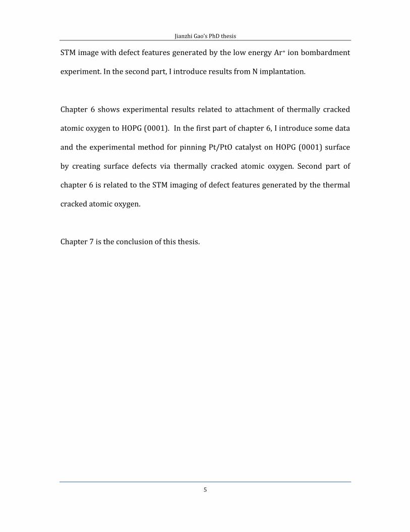
2.1 Au (111) Gold is one of the most popular metal substrates for surface science studies. This is
because gold is the only face-centred cubic (FCC) metal to present a reconstructed
structure on its (111) surface. Figure 2.1 gives a ball model showing the basic
structural information of gold. A typical FCC unit cell is shown in figure 2.1 (a),
where the blue balls are the corner atoms in the unit cell and the red balls are the
atoms at the centre of the faces. The grey triangle inside the unit cell represents the
(111) plane. Figure 2.1 (b) gives the top view of the grey triangle, which consists of
hexagonally close-packed gold atoms. Major crystallographic directions are
illustrated with double-headed arrows.
The earliest experimental studies of the physical properties of Au(111) used low-
energy electron diffraction (LEED) [44,45] and reflection high-energy electron
diffraction (RHEED) [46]. These studies identified features appearing with a 6.3 nm
periodicity on the top-most layer. This gives the first evidence that the Au(111)
surface is reconstructed.
Jianzhi Gao’s PhD thesis
7
(a)
(b)
Figure 2.1: (a) Ball model of unit the FCC cell of bulk lattice structure of gold, the (111) plane is
shown by the grey coloured plane. (b) Top view of the grey plane in (a) with the major
crystallographic directions shown.
[ ]
[ ]
[ ]
[ ]
[ ] [ ]
[ 1]
[ ]
[ ]
[ ]
[ 11] [ ]
Jianzhi Gao’s PhD thesis
8
The unit cell of reconstructed Au(111) is a rectangular (22 × √3) superlattice, with a
4.55% uniaxial contraction along one of three equivalent <110> directions. This was
confirmed by later transmission electron microscopy (TEM) experiments [47, 48]. M.
A. van Hove et al. [45] interpreted this reconstruction feature using a stacking-fault
model, with the atoms in the surface layer alternately occupying ABC stacking (FCC-
type) sites and ABA stacking (HCP-type) sites. In addition, the three-fold symmetry
of the LEED diffraction pattern is explained as the superposition of three domains
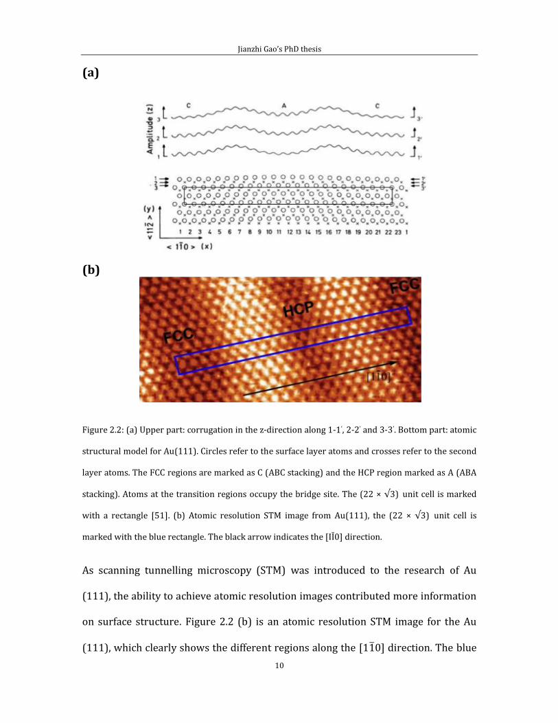
that are 120o rotated relative to each other. Figure 2.2 (a) [49] is a structural model
of the Au(111) surface, based on the stacking fault idea [50]. This model allows FCC
regions and HCP regions to coexist in the same unit cell.
In the lower part of figure 2.2 (a), circles refer to the top layer atoms and crosses
refer to the second layer atoms. There is a black rectangle that represents the (22 ×
√3) unit cell. Z corrugations along lines 1-1’, 2-2’ and 3-3’ are shown at the upper
part of (a). Due to the contraction along the [1 0] direction, there are 23 atoms
occupying 22 bulk lattice positions along the side of the (22 × √3) unit cell. The
distance between adjacent surface Au atoms along the [1 0] direction is not uniform
because atoms have the tendency to stay at three-fold hollow sites. The outcome is
that some atoms on the surface stay at FCC hollow sites and some at HCP hollow site.
Atoms at transition regions between the FCC and HCP regions occupy the bridge site.
Therefore some atoms are slightly displaced along the [11 ] direction. There is also
a periodic change in the vertical corrugation.
Jianzhi Gao’s PhD thesis
9
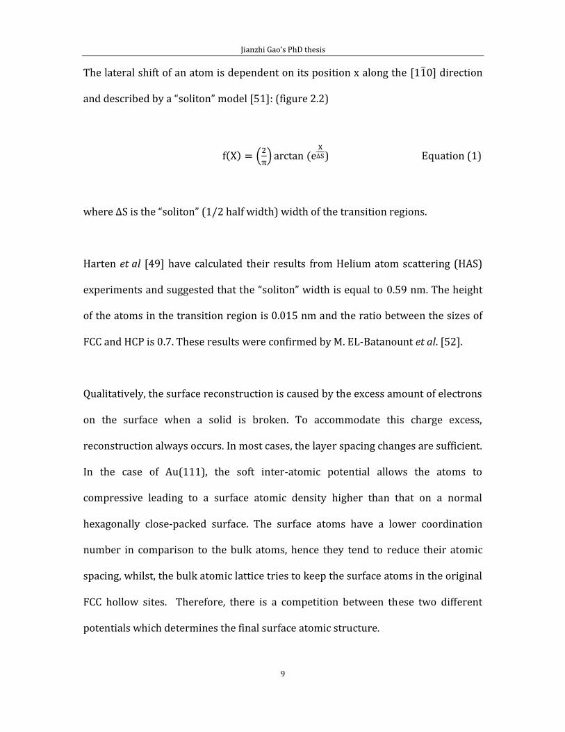
The lateral shift of an atom is dependent on its position x along the [1 0] direction
and described by a “soliton” model [51]: (figure 2.2)
) Equation (1)
where ΔS is the “soliton” (1/2 half width) width of the transition regions.
Harten et al [49] have calculated their results from Helium atom scattering (HAS)
experiments and suggested that the “soliton” width is equal to 0.59 nm. The height
of the atoms in the transition region is 0.015 nm and the ratio between the sizes of
FCC and HCP is 0.7. These results were confirmed by M. EL-Batanount et al. [52].
Qualitatively, the surface reconstruction is caused by the excess amount of electrons
on the surface when a solid is broken. To accommodate this charge excess,
reconstruction always occurs. In most cases, the layer spacing changes are sufficient.
In the case of Au(111), the soft inter-atomic potential allows the atoms to
compressive leading to a surface atomic density higher than that on a normal
hexagonally close-packed surface. The surface atoms have a lower coordination
number in comparison to the bulk atoms, hence they tend to reduce their atomic
spacing, whilst, the bulk atomic lattice tries to keep the surface atoms in the original
FCC hollow sites. Therefore, there is a competition between these two different
potentials which determines the final surface atomic structure.
Jianzhi Gao’s PhD thesis
10
(a)
(b)
Figure 2.2: (a) Upper part: corrugation in the z-direction along 1-1’, 2-2’ and 3-3’. Bottom part: atomic
structural model for Au(111). Circles refer to the surface layer atoms and crosses refer to the second
layer atoms. The FCC regions are marked as C (ABC stacking) and the HCP region marked as A (ABA
stacking). Atoms at the transition regions occupy the bridge site. The (22 × √3) unit cell is marked
with a rectangle [51]. (b) Atomic resolution STM image from Au(111), the (22 × √3) unit cell is
marked with the blue rectangle. The black arrow indicates the [IĪ0] direction.
As scanning tunnelling microscopy (STM) was introduced to the research of Au
(111), the ability to achieve atomic resolution images contributed more information
on surface structure. Figure 2.2 (b) is an atomic resolution STM image for the Au
(111), which clearly shows the different regions along the [1 0] direction. The blue
Jianzhi Gao’s PhD thesis
11
rectangle shows the (22 × √3) unit cell. This STM image is in good agreement with
the model in (a). The nearest neighbour distance of gold atoms measured from the
image falls within the range 2.7 to 2.9 Å. This value agrees with the theoretical
simulation result of 2.7744 Å in [53].
Another important surface atomic lattice parameter can be measured by using the
STM image in figure 2.2 (b). Along a gold atomic row running along the [1 0]
direction, the stacking shift from FCC to HCP causes a displacement in the [11 ]
direction, due to the different positions of FCC and HCP sites. This lateral
displacement has a theoretical value equal to √3/6a, or about 0.83 Å where “a” is
nearest neighbour distance of un-reconstructed Au (111). The distance measured
from the STM image in figure 2.2 (b) is equal to 0.9 Å, in good agreement with the
theoretical result.
The STM image in figure 2.2 (b) shows that atoms occupying the bridge site appear
taller. Collectively, these atoms produce rows of “bright” atoms along the [11 ]
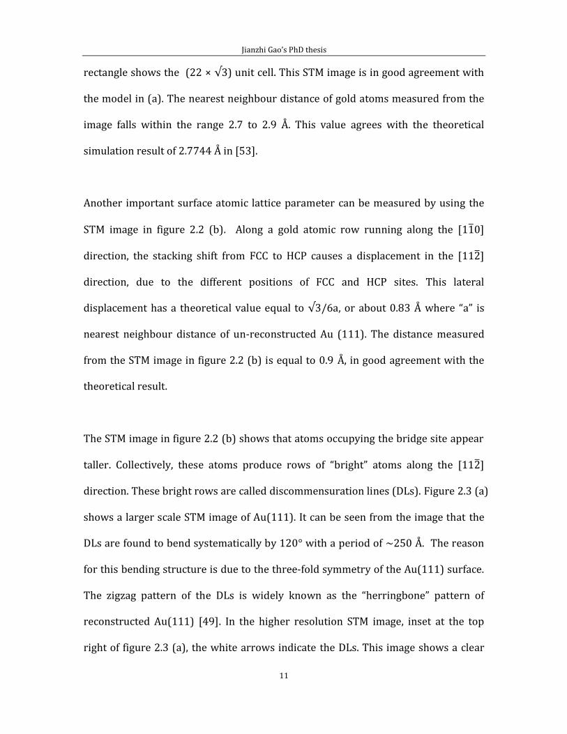
direction. These bright rows are called discommensuration lines (DLs). Figure 2.3 (a)
shows a larger scale STM image of Au(111). It can be seen from the image that the
DLs are found to bend systematically by 120° with a period of ~250 Å. The reason
for this bending structure is due to the three-fold symmetry of the Au(111) surface.
The zigzag pattern of the DLs is widely known as the “herringbone” pattern of
reconstructed Au(111) [49]. In the higher resolution STM image, inset at the top
right of figure 2.3 (a), the white arrows indicate the DLs. This image shows a clear
Jianzhi Gao’s PhD thesis
12
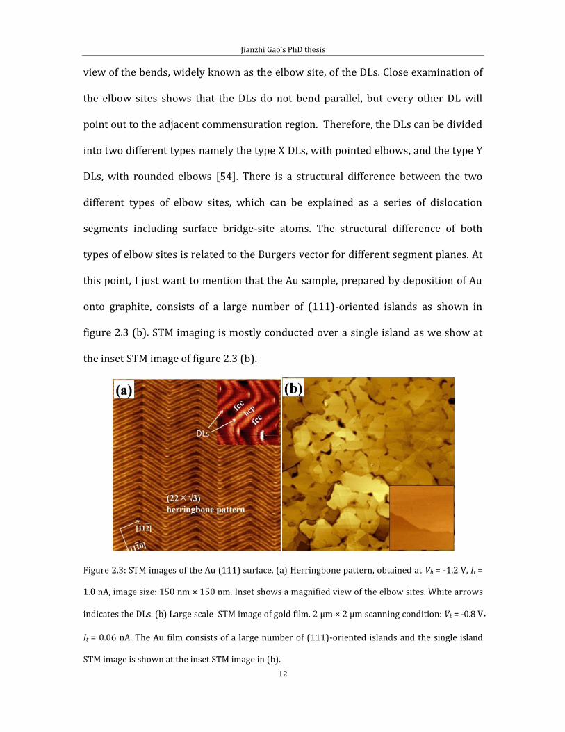
view of the bends, widely known as the elbow site, of the DLs. Close examination of
the elbow sites shows that the DLs do not bend parallel, but every other DL will
point out to the adjacent commensuration region. Therefore, the DLs can be divided
into two different types namely the type X DLs, with pointed elbows, and the type Y
DLs, with rounded elbows [54]. There is a structural difference between the two
different types of elbow sites, which can be explained as a series of dislocation
segments including surface bridge-site atoms. The structural difference of both
types of elbow sites is related to the Burgers vector for different segment planes. At
this point, I just want to mention that the Au sample, prepared by deposition of Au
onto graphite, consists of a large number of (111)-oriented islands as shown in
figure 2.3 (b). STM imaging is mostly conducted over a single island as we show at
the inset STM image of figure 2.3 (b).
Figure 2.3: STM images of the Au (111) surface. (a) Herringbone pattern, obtained at Vb = -1.2 V, It =
1.0 nA, image size: 150 nm × 150 nm. Inset shows a magnified view of the elbow sites. White arrows
indicates the DLs. (b) Large scale STM image of gold film. 2 μm × 2 μm scanning condition: Vb = -0.8 V,
It = 0.06 nA. The Au film consists of a large number of (111)-oriented islands and the single island
STM image is shown at the inset STM image in (b).
Jianzhi Gao’s PhD thesis
13
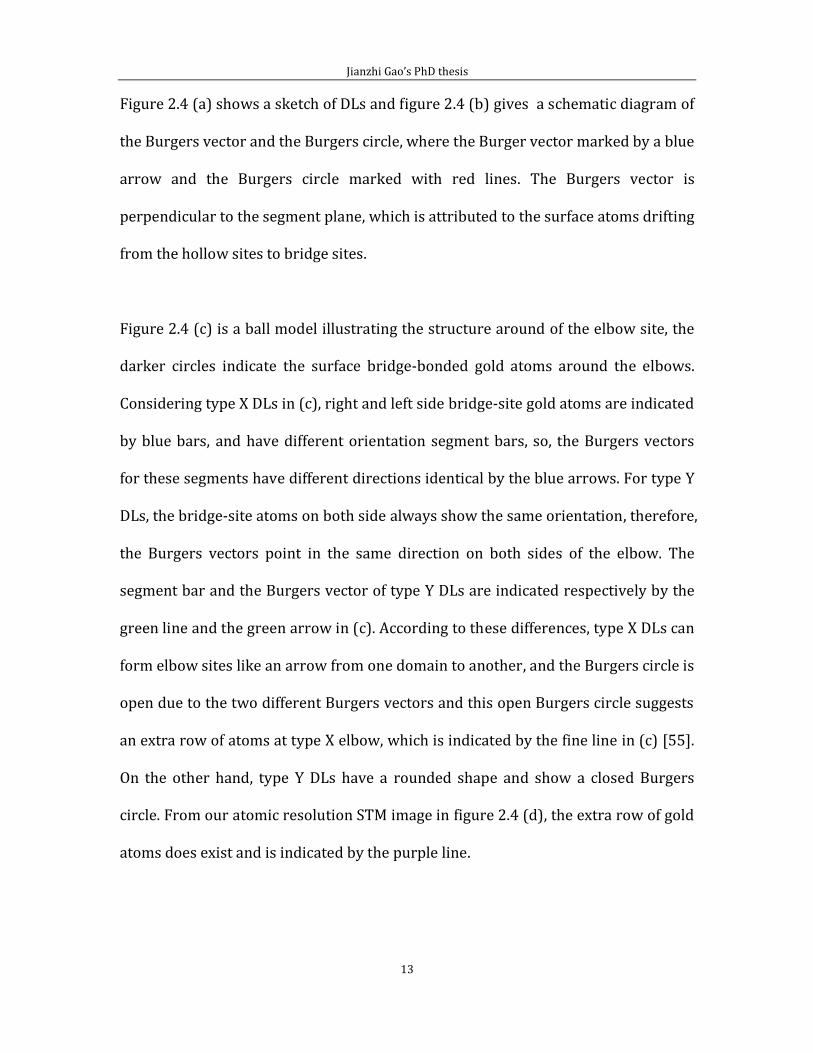
Figure 2.4 (a) shows a sketch of DLs and figure 2.4 (b) gives a schematic diagram of
the Burgers vector and the Burgers circle, where the Burger vector marked by a blue
arrow and the Burgers circle marked with red lines. The Burgers vector is
perpendicular to the segment plane, which is attributed to the surface atoms drifting
from the hollow sites to bridge sites.
Figure 2.4 (c) is a ball model illustrating the structure around of the elbow site, the
darker circles indicate the surface bridge-bonded gold atoms around the elbows.
Considering type X DLs in (c), right and left side bridge-site gold atoms are indicated
by blue bars, and have different orientation segment bars, so, the Burgers vectors
for these segments have different directions identical by the blue arrows. For type Y
DLs, the bridge-site atoms on both side always show the same orientation, therefore,
the Burgers vectors point in the same direction on both sides of the elbow. The
segment bar and the Burgers vector of type Y DLs are indicated respectively by the
green line and the green arrow in (c). According to these differences, type X DLs can
form elbow sites like an arrow from one domain to another, and the Burgers circle is
open due to the two different Burgers vectors and this open Burgers circle suggests
an extra row of atoms at type X elbow, which is indicated by the fine line in (c) [55].
On the other hand, type Y DLs have a rounded shape and show a closed Burgers
circle. From our atomic resolution STM image in figure 2.4 (d), the extra row of gold
atoms does exist and is indicated by the purple line.
Jianzhi Gao’s PhD thesis
14
Figure 2.4: (a) A sketch of the discommensuration lines (DLs), two different types of DLs are named
as X and Y respectively. Type X DLs have pointed elbows and type Y DLs have rounded elbows, and
the Burgers vectors of the segments are indicated by arrows. (b) Sketch showing the Burgers vector
of a dislocation segment. The segment bar is indicated as the blue line and the Burgers vector and
orientation is indicated as the blue arrow. (c) A ball model of the possible atomic lattice around
elbows. The blue arrows and the blue bars indicated the Burgers vectors and the segment bar around
type X DLs respectively. The green arrows and green bars are the Burgers vectors and segment bar
around type Y DLs respectively. The open and closed loops indicated the Burgers vectors for type X
and type Y DLs respectively. The fine line shows that there is an extra row of atoms at type X elbow
area. (d) An atomic resolution STM image 9 V = -0.002 V, I = 12 nA). Around a type X elbow, the row
of atoms is marked along the blue line. (e) STM image (V=-0.02 V, I=12 nA) shows the bulged and
pinched elbows.
Segment of type X DL
Segment of type Y DL
Burgers vector of type X DL
Burgers vector of type Y DL
(a)
(b) (c)
(d) (e)
Jianzhi Gao’s PhD thesis
15
This feature has also been confirmed by using the glancing-incidence and X-ray
reflectivity techniques to test discommensuration-fluid phase in [56]. Therefore, in
conclusion, there is an extra row of atoms present at every other DLs along a
domain boundary.
According to figure 2.4 (d), types X DLs point towards the FCC (HCP) regions along
one domain boundary if all the type X DLs point to the HCP (FCC) at next domain
boundary. Here, we name the type X DL pointing to an FCC region as bulged elbow
and the type X DL pointing to the HCP region as the pinched elbow. Thus the
herringbone pattern is composed of alternating rows of bulged and pinched elbows.
The reason for the formation of the periodically alternating (22 × √3) domains is
due to the balance between elastic relaxation energy and domain wall energy.
Formation of domain walls is not energetically favoured due to the disrupting of the
(22 × √3) unit cell [53]. The contraction in a single (22 × √3) domain is uniaxial and
depends on the tensile stress along the <110> direction. However, the tensile stress
remains in the orthogonal direction, which causes the overall anisotropic stress on
the surface. By forming (22 × √3) domains in three equivalent directions, surface
stress can be released in all directions. The formation of domain boundaries costs
energy to break the periodically alternating (22 × √3) contraction. Therefore, the
structure depends on the balance between the energy cost to generate domain
boundaries and the energy gain by reducing the elastic stress. Normally, the
experimentally reported periodic lengths are between 120 Å and 250 Å [54, 55, 57,
58], however, larger periodic lengths are possible. Narasimhan and Vanderbilt [53]

Jianzhi Gao’s PhD thesis
16
calculated the equilibrium periodic length using the 2D Frenkel-Kontorova model
and gave a range from 140 Å to 980 Å. What is more, the periodic length is believed
to depend on the local elastic stress environment.
In conclusion of this section, the Au(111) surface presents a complex herringbone
pattern, with a periodically alternating (22 × √3) domains and long-range
periodicity, due to surface strain domains.
2.2 Self-assembled monolayer of alkanethiol molecules In the following section. I will review the previous work on self-assembled
monolayer of alkanethioles on Au(111).
Figure 2.5: Schematic diagram of a standing-up decanethiol molecule adsorbed on Au(111) in full
coverage phases [12]. The typical angles are α = 30o , β = 55o , and χ = 14o Red: sulfur atom; blue:
carbon atom; white: hydrogen atom.
Jianzhi Gao’s PhD thesis
17
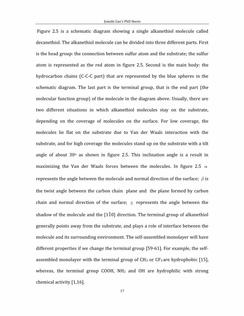
Figure 2.5 is a schematic diagram showing a single alkanethiol molecule called
decanethiol. The alkanethiol molecule can be divided into three different parts. First
is the head group: the connection between sulfur atom and the substrate; the sulfur
atom is represented as the red atom in figure 2.5. Second is the main body: the
hydrocarbon chains (C-C-C part) that are represented by the blue spheres in the
schematic diagram. The last part is the terminal group, that is the end part (the
molecular function group) of the molecule in the diagram above. Usually, there are
two different situations in which alkanethiol molecules stay on the substrate,
depending on the coverage of molecules on the surface. For low coverage, the
molecules lie flat on the substrate due to Van der Waals interaction with the
substrate, and for high coverage the molecules stand up on the substrate with a tilt
angle of about 30o as shown in figure 2.5. This inclination angle is a result in
maximizing the Van der Waals forces between the molecules. In figure 2.5 α
represents the angle between the molecule and normal direction of the surface; βis
the twist angle between the carbon chain plane and the plane formed by carbon
chain and normal direction of the surface; χ represents the angle between the
shadow of the molecule and the [1 0] direction. The terminal group of alkanethiol
generally points away from the substrate, and plays a role of interface between the
molecule and its surrounding environment. The self-assembled monolayer will have
different properties if we change the terminal group [59-61]. For example, the self-
assembled monolayer with the terminal group of CH3 or CF3 are hydrophobic [15],
whereas, the terminal group COOH, NH2 and OH are hydrophilic with strong
chemical activity [1,16].
Jianzhi Gao’s PhD thesis
18
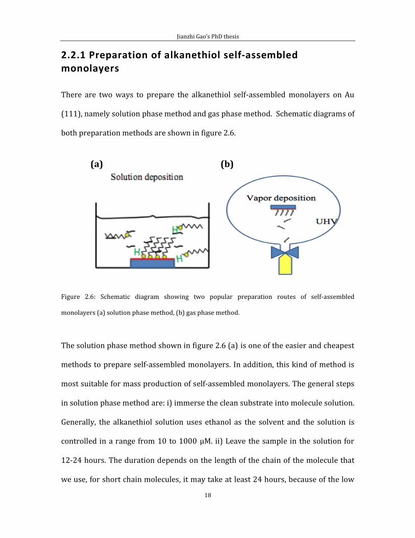
2.2.1 Preparation of alkanethiol self-assembled monolayers
There are two ways to prepare the alkanethiol self-assembled monolayers on Au
(111), namely solution phase method and gas phase method. Schematic diagrams of
both preparation methods are shown in figure 2.6.
(a) (b)
Figure 2.6: Schematic diagram showing two popular preparation routes of self-assembled
monolayers (a) solution phase method, (b) gas phase method.
The solution phase method shown in figure 2.6 (a) is one of the easier and cheapest
methods to prepare self-assembled monolayers. In addition, this kind of method is
most suitable for mass production of self-assembled monolayers. The general steps
in solution phase method are: i) immerse the clean substrate into molecule solution.
Generally, the alkanethiol solution uses ethanol as the solvent and the solution is
controlled in a range from 10 to 1000 μM. ii) Leave the sample in the solution for
12-24 hours. The duration depends on the length of the chain of the molecule that
we use, for short chain molecules, it may take at least 24 hours, because of the low
Jianzhi Gao’s PhD thesis
19
chemical activity, whereas for long chain molecules it would take a shorter time. The
immersion process makes the solution react with the surface atoms of the substrate
at room temperature and hence form the self-assembled monolayer. iii) take out
the sample and wash with ethanol to get rid of physisorbed molecules, followed by
drying with N2 gas. With this process, there are multiple factors that can affect the
efficiency of the sample growth and the structure of the self-assembled monolayer,
such as the cleanness of the substrate, the purity of the solution and the
temperature during the growth of molecular layer [1].
The gas phase method in figure 2.6 (b), requires an Ultra High Vacuum (UHV)
chamber. The gas phase method also requires the molecules to have a high vapour
pressure, hence, this kind of method is much more suitable for short chain
molecules (C< 10).
Historically, solution phase method has been the more popular method for the
preparation of self assembled monolayers. However, there are some drawbacks to
this method. One serious problem is that most of in-situ inspection methods used
are not compatible with the solution phase method. Therefore, there is limited
information we can obtain during the growth process of the self-assemble
monolayer. In contrast, the gas phase method operating inside the UHV chamber,
ensures the cleanliness of the substrate surface and gas amount is easily controlled.
Moreover, this kind of growth method is compatible with in-situ inspection methods
[62] such as Grazing incidence X-ray diffraction (GIXD), Low energy atom diffraction

Jianzhi Gao’s PhD thesis
20
(LEAD), Low energy electron diffraction (LEED), Scanning tunneling microscopy
(STM), and Temperature-programmed desorption (TPD). Therefore, the gas phase
method is much more suitable for insitu monitoring of the growth process.
2.2.2 Deposition process of alkanethiol molecules
In the work presented in this thesis, we used the gas phase method to grow
alkanethiol monolayers on the Au(111) surface, and used the variable temperature
STM to image the structure of the monolayers. To understand the self-assembly
process we need to consider the self-assembled dynamics and thermodynamics
during the growth of the monolayer. We need to consider the chemical forces
between the molecules, force between the molecules and the substrate. We need to
investigate which force plays a more significant role during the formation of the
self-assembled monolayers, and the relationship between the coverage and the
structural phases. To date, there have been many articles describing the formation
of self-assembled monolayers [12, 34, 63], here we begin by presenting a brief
overview of the deposition process of alkanethiol molecules.
When Au(111) is exposed to an alkanethiol vapour, adsorption is temperature
dependent. In most cases where the substrate is at RT (RT: room temperature),
dissociative adsorption occurs creating alkylthiolate. Under very low temperatures
[64-69], alkanethiol adsorbs molecularly without dissociation. STM images shown in
figure 2.7 show how ethanethiol molecules adsorb on Au(111) at 120 K [229]. At
this temperature, ethanethiol molecules are physisorbed.
Jianzhi Gao’s PhD thesis
21
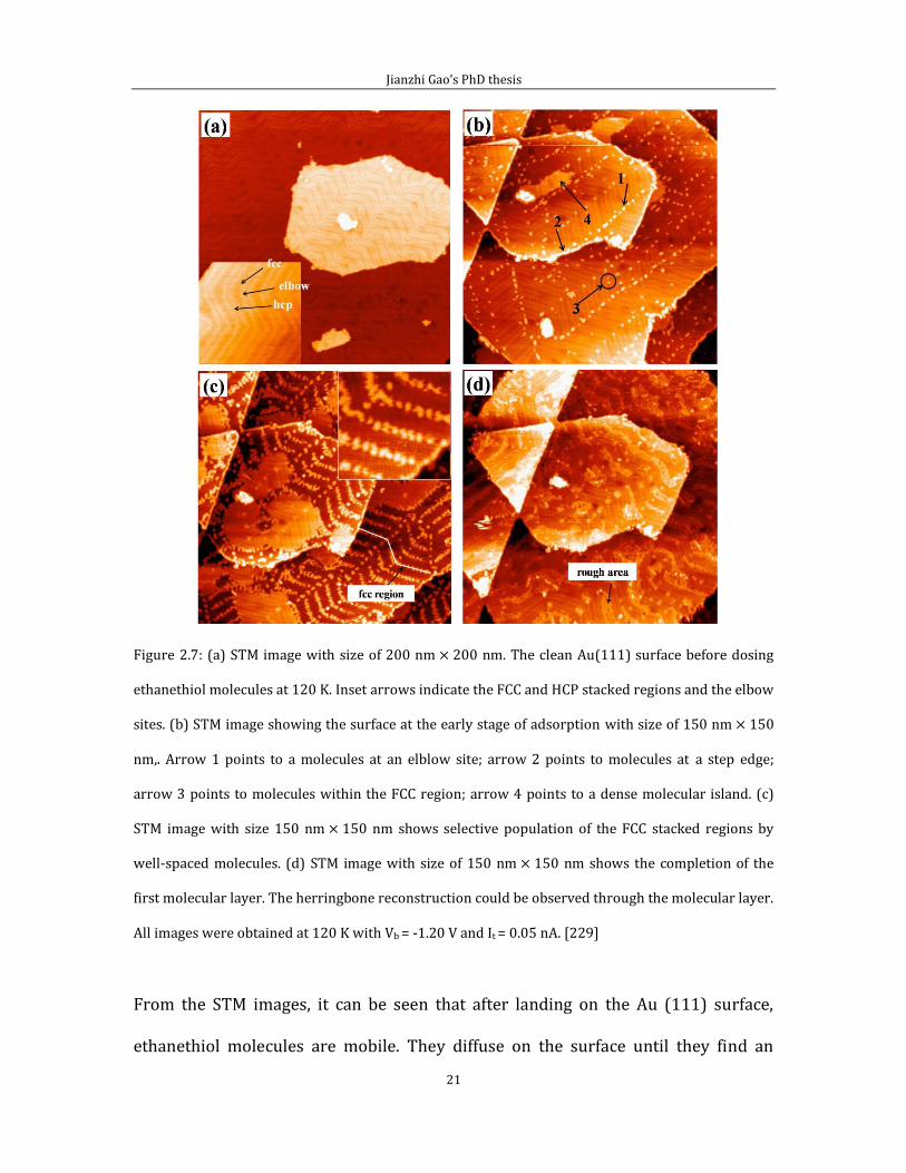
Figure 2.7: (a) STM image with size of 200 nm 200 nm. The clean Au(111) surface before dosing
ethanethiol molecules at 120 K. Inset arrows indicate the FCC and HCP stacked regions and the elbow
sites. (b) STM image showing the surface at the early stage of adsorption with size of 150 nm 150
nm,. Arrow 1 points to a molecules at an elblow site; arrow 2 points to molecules at a step edge;
arrow 3 points to molecules within the FCC region; arrow 4 points to a dense molecular island. (c)
STM image with size 150 nm 150 nm shows selective population of the FCC stacked regions by
well-spaced molecules. (d) STM image with size of 150 nm 150 nm shows the completion of the
first molecular layer. The herringbone reconstruction could be observed through the molecular layer.
All images were obtained at 120 K with Vb = -1.20 V and It = 0.05 nA. [229]
From the STM images, it can be seen that after landing on the Au (111) surface,
ethanethiol molecules are mobile. They diffuse on the surface until they find an
Jianzhi Gao’s PhD thesis
22
elbow site or a step edge. Thus at low surface coverage, the landed molecules are
attached to stronger bonding sites. There are individual molecules attached to the
elbow sites, and rows of molecules lining the step edges. As the coverage increases,
the FCC region gets populated while the HCP region remains clean. This suggests
that molecules can diffuse from the HCP region to the FCC region but not the reverse.
This indicates an asymmetric diffusion barrier where the barrier height is higher for
molecules moving from the FCC region to the HCP region. Within the FCC region,
molecules tends to stay away from each other, indicating a weak repulsive
interaction between them. Once the FCC region is fully covered, molecules begin to
occupy the HCP region and finally a whole layer is formed on the surface. When the
Au(111) surface with a layer of physisorbed molecules is warmed up to RT,
molecules desorb from the surface leaving behind an almost clean Au(111) surface.
This suggests that dissociation probability of ethanethiol on Au(111) is very low. If
Au(111) is exposed to alkanethiol vapour at RT, it leads to a different outcome. For
alkanethiols without too long a chain, physisorbed state is not stable at RT. During
exposure, one can see the chemisorbed alkylthiolate under STM, and this has been
proved from vibration spectroscopy analysis [226].
Figure 2.8 shows the growth of a mercaptohexanol monolayer on Au(111). In
comparison with the ethanethiol experiment, the mercaptohexanol monolayer was
exposure at RT. Unlike the intact molecules of ethanethiol case, the features appear
on mercaptohexanol monolayer are caused by the dissociation products. Figure 2.8
(a) shows a series of STM images for increasing exposures of mercaptohexanol
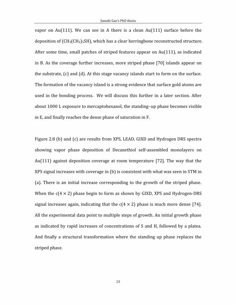
Jianzhi Gao’s PhD thesis
23
vapor on Au(111). We can see in A there is a clean Au(111) surface before the
deposition of (CH3(CH2)5SH), which has a clear herringbone reconstructed structure.
After some time, small patches of striped features appear on Au(111), as indicated
in B. As the coverage further increases, more striped phase [70] islands appear on
the substrate, (c) and (d). At this stage vacancy islands start to form on the surface.
The formation of the vacancy island is a strong evidence that surface gold atoms are
used in the bonding process. We will discuss this further in a later section. After
about 1000 L exposure to mercaptohexanol, the standing–up phase becomes visible
in E, and finally reaches the dense phase of saturation in F.
Figure 2.8 (b) and (c) are results from XPS, LEAD, GIXD and Hydrogen DRS spectra
showing vapor phase deposition of Decanethiol self-assembled monolayers on
Au(111) against deposition coverage at room temperature [72]. The way that the
XPS signal increases with coverage in (b) is consistent with what was seen in STM in
(a). There is an initial increase corresponding to the growth of the striped phase.
When the c(4 2) phase begin to form as shown by GIXD, XPS and Hydrogen-DRS
signal increases again, indicating that the c(4 2) phase is much more dense [74].
All the experimental data point to multiple steps of growth. An initial growth phase
as indicated by rapid increases of concentrations of S and H, followed by a platea.
And finally a structural transformation where the standing up phase replaces the
striped phase.
Jianzhi Gao’s PhD thesis
24
Figure 2.8: Experimental observation of the growth progress of alkanethiol monolayers on Au(111).
(a) A series of STM images for increasing exposures of mercaptohexanol vapor on Au(111) [71]. A)
Clean (22 ) “herringbone” reconstructed Au(111). B) Small patches shows striped phase
(pointing finger). C) Striped phase displaces the herringbone reconstruction. D) Continued growth of
the striped phase with Au vacancy islands (pointing finger) formation. E) Standing-up Phase becomes
visible within striped phase after about 1000L. F) Growth of standing-up phase at expense of the
striped phase until saturation. (b) Decanethiol SAM on Au(111) from vapor phase deposition as
characterized by XPS, LEAD and GIXD at room temperature [72]. (c) Hydrogen direct recoil
spectroscopy (HDRS) intensity from Au (111) as a function of exposure to hexanethiol gas [73].
Jianzhi Gao’s PhD thesis
25
2.2.3 Structural properties of self-assembled monolayers of alkanethiol molecules on Au(111) In the previous section, we described the deposition process of alkanethiol
molecules. However, the main purpose of this thesis is to investigate the structural
information of alkanethiol self-assembled monolayers using VT-STM (VT: Variable
temperature.), so in this section we focus on the structural aspects of self-assembles
monolayers (SAM).
300 With alkanethiol self-assembled monolayers, every stable structure is the result of
competitions between the chemical adsorption of the head group (-S) of the
molecule on the substrate and the Van der Waals force between the molecules.
Generally, the bulk phase of straight chain alkane molecules has a simple
orthorhombic structure, which means that the molecules are perpendicular to the
(100) plane of the molecular crystal giving the most densely molecular arrangement,
thus maximizing the Van der Waals force between the molecules. There are two
possible dense phase structures that can exist when alkanethiol or molecules are
packed on the Au(111) surface during the formation the self-assembled monolayers;
the 0 structure and its c (4 2) supper-lattice. The formation of the
0 structure was assumed as the result of the sulfur atoms of the
alkanethiol molecules arranging in a hexagonal closed-packed structure on Au(111).
The nearest neighbor distance between the sulfur atoms is 0.5 nm, which is equal to
a, where a = 0.289 nm is the atomic distance of gold atoms. According to DFT
Jianzhi Gao’s PhD thesis
26
theoretical calculations [75], the most likely adsorption site of S atoms is the FCC
hollow site. Furthermore, the distance for the bulk phase of straight chain alkane
molecules is less than 0.5 nm. When the sulfur atoms of alkanethiol molecules form
the 0 structure, there is rotation and inclination of the molecular
chains, hence maximizing the Van der Waals forces between the molecules and
making the self assembled system stable.
Early diffraction experiments [76-78], established that alkanethiol molecules can
form the 0 structures on Au(111) at saturate coverage, with all
molecules occupying the same site on the substrate, and the distance between
nearest molecules equal to 0.499 nm. Every unit cell contains one single molecule,
and the surface area of a unit cell is equal to 0.2165 nm2. From this, it is concluded
that the surface coverage at saturate absorption is ML. This means that
there is one absorbed molecule for every three gold atoms. In addition, the early
experiments [79] also studied the unit cell area of bulk phase straight chain alkane
molecules when the molecules formed the 0 structures. The results
show that the unit cell area is equal to 0.184 nm2 when projected onto (100) surface.
From this result we know that the bulk phase unit cell is smaller than the unit cell
on Au(111). This is because the molecules are incline to the <111> direction and the
inclination angle is 0. This result is in agreement with the earlier infrared and
ellipsometry experimental studies of CH2- and CH3- [80,81], which gives a tail angle
between 300 and 350 degrees. Later studies, also found that the inclination angle is
related to the length of chains [12,34,82].
Jianzhi Gao’s PhD thesis
27
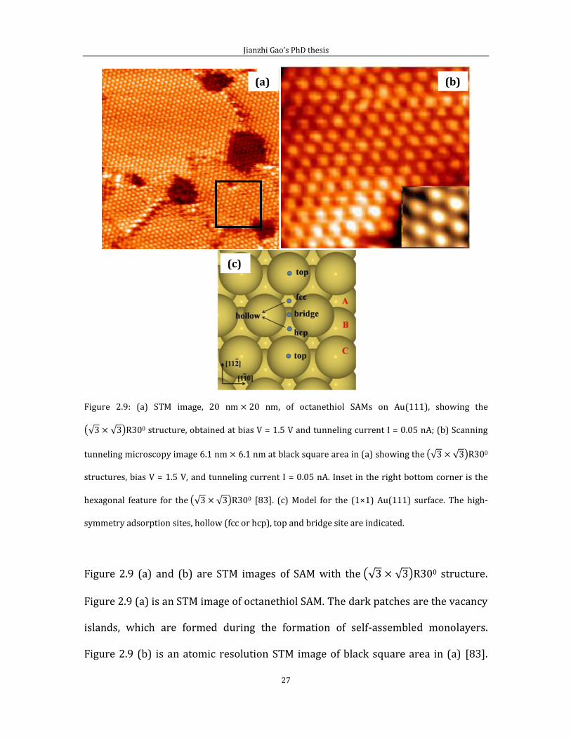
Figure 2.9: (a) STM image, 20 nm 20 nm, of octanethiol SAMs on Au(111), showing the
0 structure, obtained at bias V = 1.5 V and tunneling current I = 0.05 nA; (b) Scanning
tunneling microscopy image 6.1 nm 6.1 nm at black square area in (a) showing the 0
structures, bias V = 1.5 V, and tunneling current I = 0.05 nA. Inset in the right bottom corner is the
hexagonal feature for the 0 [83]. (c) Model for the (1×1) Au(111) surface. The high-
symmetry adsorption sites, hollow (fcc or hcp), top and bridge site are indicated.
Figure 2.9 (a) and (b) are STM images of SAM with the 0 structure.
Figure 2.9 (a) is an STM image of octanethiol SAM. The dark patches are the vacancy
islands, which are formed during the formation of self-assembled monolayers.
Figure 2.9 (b) is an atomic resolution STM image of black square area in (a) [83].
(a) (b)
(c)
Jianzhi Gao’s PhD thesis
28
The right bottom inset to this image shows the clear hexagonal feature of the
0 structure. Figure 2.9 (c) is a model for the (1 1) Au (111) surface.
The high-symmetry adsorption sites, hollow (FCC or HCP), top and bridge sites are
indicated, where FCC site is the most possible adsorption site for the alkanethiol
molecules, as we mentioned earlier.
According to the STM images in figures 2.9 (a) and (b), all the bright spot appear
identical, each one of them represents the position of a single adsorbed molecule.
We need to point it out that there are some drawbacks when we used the STM to
study the adsorption position of alkanethiol molecules. The STM can only reflect the
local charge density of the adsorbed molecules. Therefore, the bright features on the
STM images in (a) and (b) could belong to the terminal group, the hydrocarbon
chain (-CH2-) or the head part (S atom) of the adsorbed alkanethiol molecules, and,
the actual part of the molecules that is seen in the STM image is still not completely
resolved to this day [84-92]. In chapter 4, we confirm that the bright features are
belong to the (-CH3-). Liu did a series of experiments to study the structures of
alkanethiol molecules under different scanning conditions [90,91]. They found that
molecules with different terminal groups molecules, such as –COOH [83, 93-95] and
–NH2 [96], can also form the 0 phase.
Jianzhi Gao’s PhD thesis
29
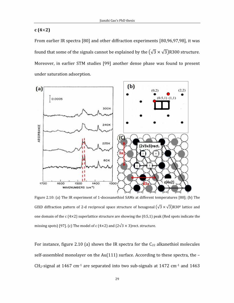
c (4 2) From earlier IR spectra [80] and other diffraction experiments [80,96,97,98], it was
found that some of the signals cannot be explained by the 0 structure.
Moreover, in earlier STM studies [99] another dense phase was found to present
under saturation adsorption.
Figure 2.10: (a) The IR experiment of 1-docosanethiol SAMs at different temperatures [80]; (b) The
GIXD diffraction pattern of 2-d reciprocal space structure of hexagonal 0 lattice and
one domain of the c (4 2) superlattice structure are showing the (0.5,1) peak (Red spots indicate the
missing spots) [97]. (c) The model of c (4 2) and (2 3)rect. structure.
For instance, figure 2.10 (a) shows the IR spectra for the C22 alkanethiol molecules
self-assembled monolayer on the Au(111) surface. According to these spectra, the –
CH2-signal at 1467 cm-1 are separated into two sub-signals at 1472 cm-1 and 1463
2
Jianzhi Gao’s PhD thesis
30
cm-1 when the substrate temperature decrease to 225 K. This shows that there are
two different molecule chain structures in the lattice structure, different from the
0 structure. This structure is the super-lattice c (4 2) structure,
which has also been confirmed by GIXD [97] and LEAD [100] experiments. The c (4
2) structure can be represented alternatively by a notation.
The c (4 2) structure is connected to the 0 structure. This kind of
structure can be formed under the same coverage as the 0 structure,
of ML. The size of the unit cell is: 9.994 8.655 , which
is four times larger than the 0 lattice structure. Therefore, there are
four molecules included in this unit cell.
Generally, surface diffraction experiments are useful to study surface periodic
structures. According to the schematic representation of the GIXD diffraction
pattern [97] in figure 2.10 (b). The GIXD diffraction pattern of 2D space structure of
hexagonal 0 lattice structure and one domain of the c (4 2)
superlattice structure are showing the (0.5,1) peak. However, for the c (4 2)
structure, some of the diffraction points are missing, such as (0,1) and (1,2) red
spots in figure 2.10 (b). These missing point coordinates, follow the rule that;
“h+k=odd number”. If we set the missing points as (h,k). Therefore, if we assume the
length of the lattice axis of . as: a 2b, then, parallel vertical can exist
Jianzhi Gao’s PhD thesis
31
at (a/2,b/2) inside the . lattice, which means we could find the same
state molecules “(x,y)” at position (x+a/2,y+b/2) as in the model in figure 2.10 (c).
According to figure 2.10 (c), molecules 1, 2, 3 and 4 are the same state molecules.
We divide these molecules as two groups as two different colors to represent the
zigzag adsorption form. This indicates that there are two different groups of
molecules inside the structure, with two molecules in each group.
This has been confirmed by IR [80], LEAD [100], and STM [86,87] experiments.
Furthermore, the LEAD experiment, which is particularly sensitive to the terminal
group of molecules, showed there are height differences between the terminal
groups of c (4 2) structure. Based on IR and LEAD experimental results, a model
was proposed to explain the formation of the c (4 2) structure. This model
proposes that the second molecule has a rotational angle (900 difference) inside
the unit cell of structure. However, this model cannot explain the
missing points in the diffraction experiment in (b), because the rotational angle
can only slightly change the brightness of the diffraction points, not make them to
disappear. Therefore, this indicates that the adsorption position of the S atoms must
have a displacement between the structure and the 0
structure.
From another GIXD experimental result in [101], it was proposed that the
alkanethiol molecules are adsorbed as disulfide on the Au(111) surface and the
distance between the S-S bonds is 0.22 nm, where one of the “S” atom is located on
Jianzhi Gao’s PhD thesis
32
the FCC site and the other at the bridge site. Although, this result was supported by a
later TPD study in [102], the existence of the S-S bonds in self-assembled
monolayers has been questioned. Indeed, some experiments disapproved this
disulfide model. [74,103,104] To explain the experimental results of GIXD, Torrelles’
team [74] proposed another model based on the possibility that some of the
molecules are located on the top site and another half stay at the FCC site in the
structure. What is more, the reconstruction structure on the Au(111)
surface can also affect the formation of the structure.
In comparison to diffraction experiments, the investigation of the c (4 2) structure
by STM is much more complicated. Since the discovery of the c (4 2) structure by
Nuzzo [80], there have been at least five different c (4 2) structures found. All of
these structures correspond to the . lattice constants, however, with
slight differences in their internal unit cell structures, as evidenced by variations in
brightness contrast in STM images [87]. As a result, many different models [20] have
been proposed to explain these c (4 2) structures, However, there so far is no
agreement on the explanation for the relationship between c (4 2) structures and
that of the 0.
Other STM studies on different terminal groups’ alkanethiol molecules, such as –
COOH [95], -OH, and –NH2, also exhibit c (4 2) structures on the Au(111) surface.
So, different molecules’ terminal groups do not seem to affect the formation of the c
Jianzhi Gao’s PhD thesis
33
(4 2) structure. This may be because the formation of c (4 2) structure is due to
the shifting of the S part of the molecule.
Transformation between c (4 2) and 0
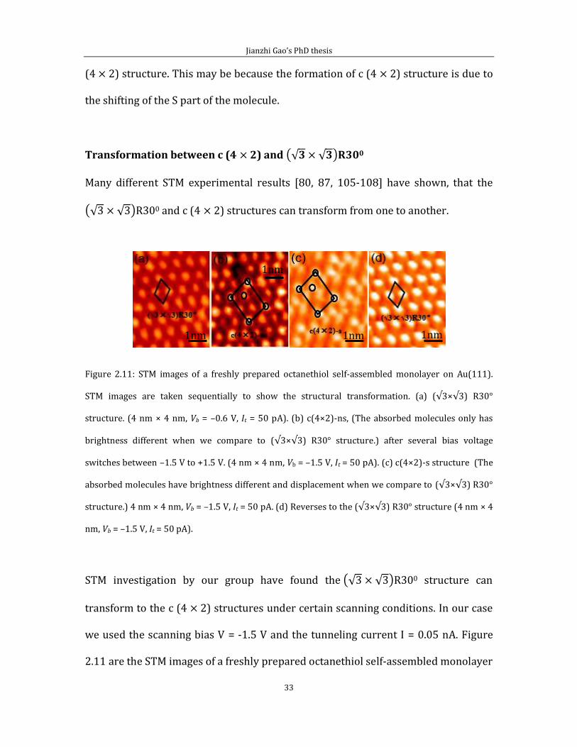
Many different STM experimental results [80, 87, 105-108] have shown, that the
0 and c (4 2) structures can transform from one to another.
Figure 2.11: STM images of a freshly prepared octanethiol self-assembled monolayer on Au(111).
STM images are taken sequentially to show the structural transformation. (a) (√3×√3) R30°
structure. (4 nm × 4 nm, Vb = –0.6 V, It = 50 pA). (b) c(4×2)-ns, (The absorbed molecules only has
brightness different when we compare to (√3×√3) R30° structure.) after several bias voltage
switches between –1.5 V to +1.5 V. (4 nm × 4 nm, Vb = –1.5 V, It = 50 pA). (c) c(4×2)-s structure (The
absorbed molecules have brightness different and displacement when we compare to (√3×√3) R30°
structure.) 4 nm × 4 nm, Vb = –1.5 V, It = 50 pA. (d) Reverses to the (√3×√3) R30° structure (4 nm × 4
nm, Vb = –1.5 V, It = 50 pA).
STM investigation by our group have found the 0 structure can
transform to the c (4 2) structures under certain scanning conditions. In our case
we used the scanning bias V = -1.5 V and the tunneling current I = 0.05 nA. Figure
2.11 are the STM images of a freshly prepared octanethiol self-assembled monolayer
1nm
1nm
1nm 1nm
Jianzhi Gao’s PhD thesis
34
on Au(111) which shown the transformation between 0 structure and
the c (4 2) structure. According to this sequence of images, the 0
structure transforms to the c (4 2)-ns structure first, and then to the c (4 2)-s
structure. Therefore, we can view the c (4 2)-ns structure as an intermediate
phase in the transformation between the o and the c (4 2).
Furthermore, the transformations of these structures is reversible, which means
that the energy difference between them is very small.
The (3 4) structure of SAMs from short chain alkanethiol molecules Generally, for long chain molecules (n > 3), there are three main structures that can
be observed [12,34,109]: 0, c (4 2) dense phase under the
saturation coverage, and p(m ) striped phases under low coverages. For many
years, it has been assumed that the 0 and its associated c(4 2)/(3
2 )-rect. structures are common for all alkanethiol SAMs on Au(111) regardless
the chain length. However, recent studies have provided clear evidence that SAMs of
methylthiolate and ethylthiolate do not form these “standard” structures. Rather, a
(3 4) phase is identified as the only stable phase at saturation coverage. 3 4
means the unit cell is a quadrilateral shape, with side length equal to 3a 4a. This
kind of structure has the same coverage as the 0 structure and has
been detected by many different experimental methods, such as STM [64, 66, 68, 69,
110,111,112], LEED [113,114,118], and He atom scattering [113-115]. However the,
(3 4) structure has not been discovered in the long chain (n>2) alkanethiol
molecule’s self-assemble monolayer. [116,117]
Jianzhi Gao’s PhD thesis
35
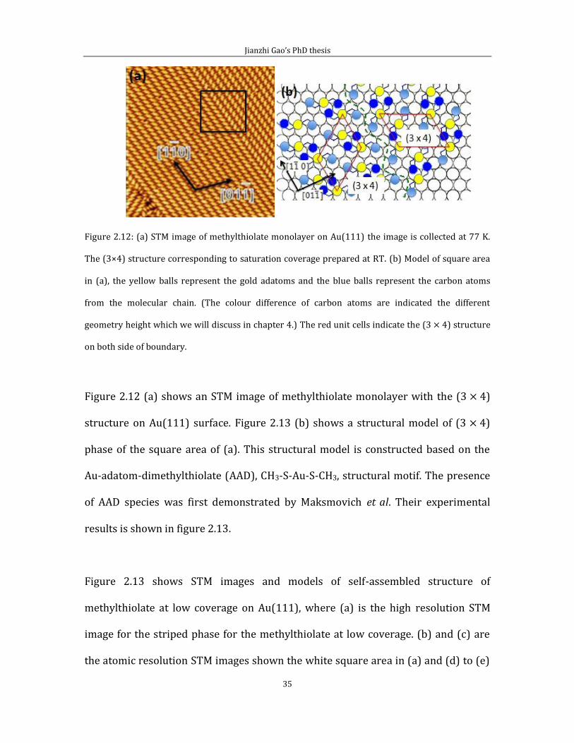
Figure 2.12: (a) STM image of methylthiolate monolayer on Au(111) the image is collected at 77 K.
The (3×4) structure corresponding to saturation coverage prepared at RT. (b) Model of square area
in (a), the yellow balls represent the gold adatoms and the blue balls represent the carbon atoms
from the molecular chain. (The colour difference of carbon atoms are indicated the different
geometry height which we will discuss in chapter 4.) The red unit cells indicate the (3 4) structure
on both side of boundary.
Figure 2.12 (a) shows an STM image of methylthiolate monolayer with the (3 4)
structure on Au(111) surface. Figure 2.13 (b) shows a structural model of (3 4)
phase of the square area of (a). This structural model is constructed based on the
Au-adatom-dimethylthiolate (AAD), CH3-S-Au-S-CH3, structural motif. The presence
of AAD species was first demonstrated by Maksmovich et al. Their experimental
results is shown in figure 2.13.
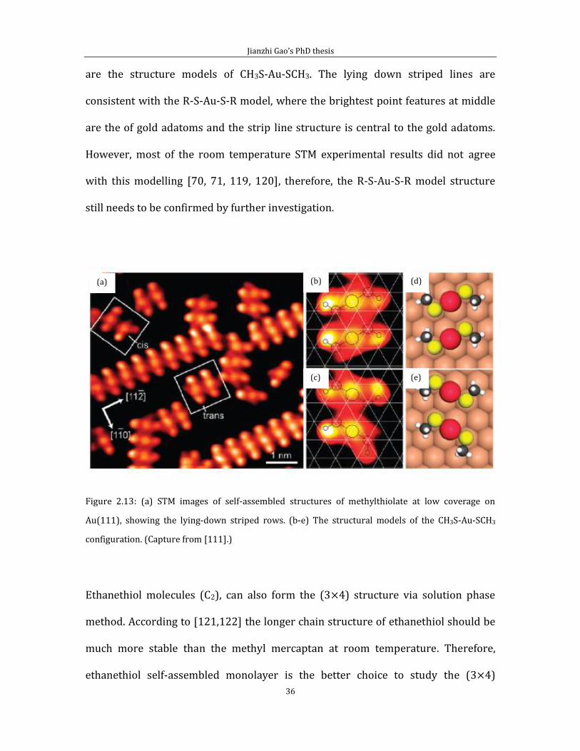
Figure 2.13 shows STM images and models of self-assembled structure of
methylthiolate at low coverage on Au(111), where (a) is the high resolution STM
image for the striped phase for the methylthiolate at low coverage. (b) and (c) are
the atomic resolution STM images shown the white square area in (a) and (d) to (e)
Jianzhi Gao’s PhD thesis
36
are the structure models of CH3S-Au-SCH3. The lying down striped lines are
consistent with the R-S-Au-S-R model, where the brightest point features at middle
are the of gold adatoms and the strip line structure is central to the gold adatoms.
However, most of the room temperature STM experimental results did not agree
with this modelling [70, 71, 119, 120], therefore, the R-S-Au-S-R model structure
still needs to be confirmed by further investigation.
Figure 2.13: (a) STM images of self-assembled structures of methylthiolate at low coverage on
Au(111), showing the lying-down striped rows. (b-e) The structural models of the CH3S-Au-SCH3
configuration. (Capture from [111].)
Ethanethiol molecules (C2), can also form the (3 4) structure via solution phase
method. According to [121,122] the longer chain structure of ethanethiol should be
much more stable than the methyl mercaptan at room temperature. Therefore,
ethanethiol self-assembled monolayer is the better choice to study the (3 4)
(a) (b)
(c)
(d)
(e)
Jianzhi Gao’s PhD thesis
37
structure and investigate the relationship with the 0 structure.
However, there have been few related investigations contributed to date.
Hagenstrom’s group [121] observed the coexistence of the (3 4) structure and
p(7.5 ) striped phase using STM at room temperature. However their STM
images have very low resolution; hence, they did not give the details of the
adsorption model. De Renzi’s group calculated the (3 4) structure using DFT; their
double adsorption sites model found 75% of molecules are located on the bridge
sites and rest are adsorbed on the top sites. However, their model does not match
with the STM images of Kawasaki’s group. Voznyy’s group proposed the RS-Au-SR
model [111] when they study the (3 4) structure for methyl mercaptan self
assembled monolayers. Their assumption is consistent with our C2 experiment, but
so far, there has not been general agreement on the adsorption model of the (3 4)
structure.
Low coverage striped phases As we mentioned in the previous sections, for the long chain molecules (n > 2), there
are three main structures that can be observed for the self assembled monolayer on
Au(111): 0, c (4 2) dense phase under the saturation absorption, and
p(m ) strip phases, with different periodicity under the low coverage
absorption, where “m” generally represents ratio between the period of the striped
phases along the orientation of Au(111) unit cell’s vectors and unit cell distance a.
Usually, “m” is equal to integer or half integer. There are two different types of
striped phase: lie down striped phase at low coverage and standing up striped phase
Jianzhi Gao’s PhD thesis
38
at higher coverage, as described earlier section 2.2.2. What is more, there are two
ways to form the striped phases, absorbing the target molecules on the substrate
with low coverage (Before the saturate absorption) [71] or desorbing the saturate
dense phases via the annealing process. Sometimes, several different periodic
striped phases can be formed by one type of molecule. Multiple types of striped
phases have been found so far, namely m= 4, 5, 6, 7.5, 9, 9.5, 11, 11.5, and 13
[70,71,85,92,119,123-131].
According to the m value, which is proportional to the chain length of molecules, the
larger molecules will need more space to fit in, as demonstrated the C10 alkanethiol
molecule striped phase. According to STM [131] and LEAD [71,132] experimental
results, the m value of C10 alkanethiol molecule’s striped phase is equal to 11, which
means the periodicity of this striped phase is equal to 3.17 nm larger than twice the
length of C10 molecule’s chain. The carbon chain of the alkanethiol molecules are not
necessary perpendicular to the [112 ] direction, they could be arranged in certain
rotational angles or even aligned in zigzag shape [125]. The purpose of these kinds
of arrangements is to maximize the Van der Waal forces between the molecules.
Figure 2.14 (a) is an STM image of decanethiol alkanthiol molecules in the lie down
striped phase; two black lines indicated the period of the striped phase. (b) is
structure model for the lying-down striped phase in (a), where two red lines
indicate the absorption sites of the S atoms. According to the structure models of
striped phases, the S atoms of the molecule are adjacent to each other [70, 71, 119,
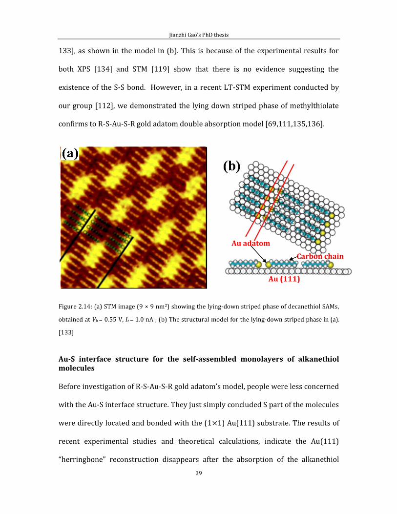
Jianzhi Gao’s PhD thesis
39
133], as shown in the model in (b). This is because of the experimental results for
both XPS [134] and STM [119] show that there is no evidence suggesting the
existence of the S-S bond. However, in a recent LT-STM experiment conducted by
our group [112], we demonstrated the lying down striped phase of methylthiolate
confirms to R-S-Au-S-R gold adatom double absorption model [69,111,135,136].
Figure 2.14: (a) STM image (9 × 9 nm2) showing the lying-down striped phase of decanethiol SAMs,
obtained at Vb = 0.55 V, It = 1.0 nA ; (b) The structural model for the lying-down striped phase in (a).
[133]
Au-S interface structure for the self-assembled monolayers of alkanethiol molecules Before investigation of R-S-Au-S-R gold adatom’s model, people were less concerned
with the Au-S interface structure. They just simply concluded S part of the molecules
were directly located and bonded with the (1 1) Au(111) substrate. The results of
recent experimental studies and theoretical calculations, indicate the Au(111)
“herringbone” reconstruction disappears after the absorption of the alkanethiol
Au (111)
Au adatom
Carbon chain
Jianzhi Gao’s PhD thesis
40
molecules, and the absorption progress can generate other reconstruction
structures, such as Au adatoms [12, 137, 138]. Therefore, we would like to briefly
discuss the absorption model of gold reconstruction where the Au-S interface model
is based on Maksymovych [137] and Vericat’s review [12].
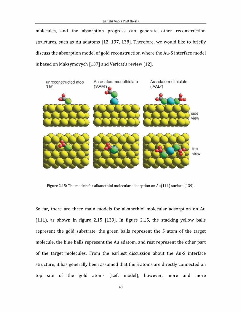
Figure 2.15: The models for alkanethiol molecular adsorption on Au(111) surface [139].
So far, there are three main models for alkanethiol molecular adsorption on Au
(111), as shown in figure 2.15 [139]. In figure 2.15, the stacking yellow balls
represent the gold substrate, the green balls represent the S atom of the target
molecule, the blue balls represent the Au adatom, and rest represent the other part
of the target molecules. From the earliest discussion about the Au-S interface
structure, it has generally been assumed that the S atoms are directly connected on
top site of the gold atoms (Left model), however, more and more
Jianzhi Gao’s PhD thesis
41
[69,104,108,111,139-144] experimental analysis have proved the existence of Au
adatoms that remain at the S-Au interface. Therefore, two different absorption
models have been proposed to explain the experimental results: RS-Au (Middle)
model and RS-Au-SR model (Right). The RS-Au model indicates that 1/6 ML gold
adatoms are adjacent to single molecules, the S atom is located on top of the gold
adatom, and the entre RS-Au unit structure is located on the FCC/hollow site of the
gold substrate [104,145]. In comparison, R-S-Au-S-R absorption model indicates
there are two alkyl mercaptides connected with the gold adatom, where the gold
adatom is located on the bridge site of the (1 1) Au(111) and two S atoms are
absorbed on the top sites on the gold substrate, as shown in the right model of
figure 2.15. The work presented in this thesis follows the R-S-Au-S-R absorption
model, as the double absorption model is much more stable than the single
absorption one (Detailed data analysis is shown in chapter 4.) [12]. However, the
general agreement of the absorption model of alkanethiol molecules is still requires
further investigation.
The previous introduction is related to the first part of my research. The second part
of my research involves doping of N and O on the top surface of graphite/graphene.
We are trying to investigate the structural and electronic properties for the C-N/C-O
bonding structures by using the scanning tunnelling microscope. The development
of current technologies for the semiconductor industry is heavily focused on silicon.
However, further progress in this field is tracing a bottleneck and approaching to
some fundamental limitations, for instant the concentration of the charge carrier,
Jianzhi Gao’s PhD thesis
42
which supports the electronic field effect in silicon [4]. On the other hand, the
graphitic materials are attracting a lot of attention due to their potential
applications in nanotechnology. Previously, more than 70 years ago, Landau and
Peierls stated the concept that two-dimensional (2D) crystals could not exist [146]
because they are thermodynamically unstable [147-149]. Moreover, this concept
was extended later by Mermin [150].
Traditionally, atomic monolayer is always produced on a solid substrate, so it
becomes an integral part of the larger 3D structure. In 2004. Geim and Novoselov
from the University of Manchester discovered exfoliation graphene with single-,
double- and few-(3 to <10) layers. They found that this 2D material of carbon has
very high electron mobility and zero band gap [4]. Normally, carbon atoms are
coupling in several different forms which exist in our daily life, such as the carbon
atoms in graphite/graphene are informed in honeycomb lattice (for a signal layer)
with sp2 electronic structure, the carbon atoms inside the diamond are shown the
sp3 electronic structure and the carbon atoms which take the random atomic
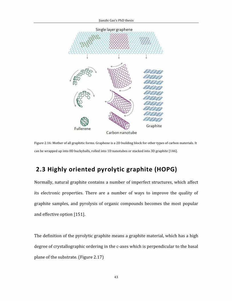
arrangement are belong to amorphous graphite. Figure 2.16 illustrates how
graphene is related to other forms of carbon.
Because graphene is closely related to graphite and properties of graphite have been
studied for many years, therefore, in the following section, I will give a
comprehensive review on previous knowledge about the structure and physical
properties of graphite.
Jianzhi Gao’s PhD thesis
43
Figure 2.16: Mother of all graphitic forms. Graphene is a 2D building block for other types of carbon materials. It
can be wrapped up into 0D buckyballs, rolled into 1D nanotubes or stacked into 3D graphite [146].
2.3 Highly oriented pyrolytic graphite (HOPG)
Normally, natural graphite contains a number of imperfect structures, which affect
its electronic properties. There are a number of ways to improve the quality of
graphite samples, and pyrolysis of organic compounds becomes the most popular
and effective option [151].
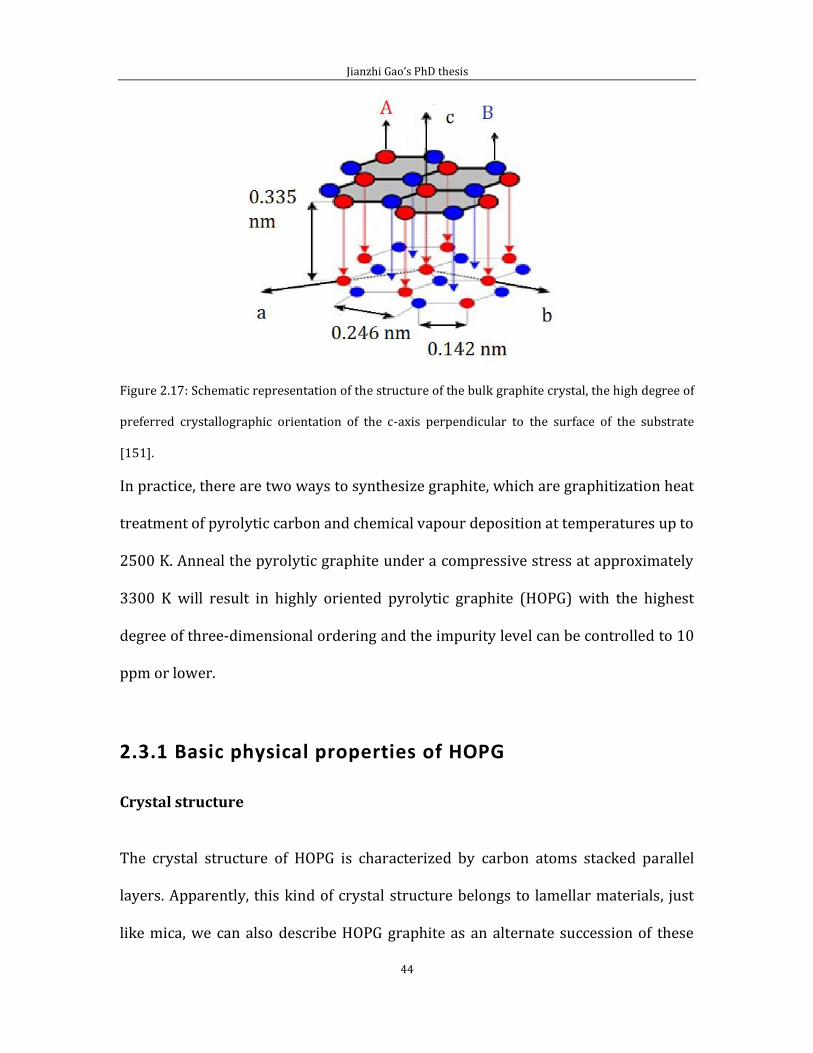
The definition of the pyrolytic graphite means a graphite material, which has a high
degree of crystallographic ordering in the c-axes which is perpendicular to the basal
plane of the substrate. (Figure 2.17)
Jianzhi Gao’s PhD thesis
44
Figure 2.17: Schematic representation of the structure of the bulk graphite crystal, the high degree of
preferred crystallographic orientation of the c-axis perpendicular to the surface of the substrate
[151].
In practice, there are two ways to synthesize graphite, which are graphitization heat
treatment of pyrolytic carbon and chemical vapour deposition at temperatures up to
2500 K. Anneal the pyrolytic graphite under a compressive stress at approximately
3300 K will result in highly oriented pyrolytic graphite (HOPG) with the highest
degree of three-dimensional ordering and the impurity level can be controlled to 10
ppm or lower.
2.3.1 Basic physical properties of HOPG
Crystal structure
The crystal structure of HOPG is characterized by carbon atoms stacked parallel
layers. Apparently, this kind of crystal structure belongs to lamellar materials, just
like mica, we can also describe HOPG graphite as an alternate succession of these
Jianzhi Gao’s PhD thesis
45
identical stacked planes. For a better understanding of the physical properties of
graphite, we need to consider the crystal structure of graphite in two aspects,
namely longitude and latitude.
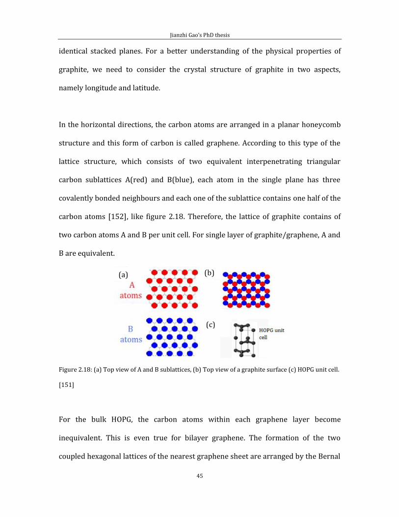
In the horizontal directions, the carbon atoms are arranged in a planar honeycomb
structure and this form of carbon is called graphene. According to this type of the
lattice structure, which consists of two equivalent interpenetrating triangular
carbon sublattices A(red) and B(blue), each atom in the single plane has three
covalently bonded neighbours and each one of the sublattice contains one half of the
carbon atoms [152], like figure 2.18. Therefore, the lattice of graphite contains of
two carbon atoms A and B per unit cell. For single layer of graphite/graphene, A and
B are equivalent.
Figure 2.18: (a) Top view of A and B sublattices, (b) Top view of a graphite surface (c) HOPG unit cell.
[151]
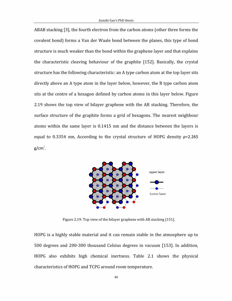
For the bulk HOPG, the carbon atoms within each graphene layer become
inequivalent. This is even true for bilayer graphene. The formation of the two
coupled hexagonal lattices of the nearest graphene sheet are arranged by the Bernal
(a) (b)
(c)
Jianzhi Gao’s PhD thesis
46
ABAB stacking [3], the fourth electron from the carbon atoms (other three forms the
covalent bond) forms a Van der Waale bond between the planes, this type of bond
structure is much weaker than the bond within the graphene layer and that explains
the characteristic cleaving behaviour of the graphite [152]. Basically, the crystal
structure has the following characteristic: an A type carbon atom at the top layer sits
directly above an A type atom in the layer below, however, the B type carbon atom
sits at the centre of a hexagon defined by carbon atoms in this layer below. Figure
2.19 shows the top view of bilayer graphene with the AB stacking. Therefore, the
surface structure of the graphite forms a grid of hexagons. The nearest neighbour
atoms within the same layer is 0.1415 nm and the distance between the layers is
equal to 0.3354 nm, According to the crystal structure of HOPG density ρ=2.265
g/cm3.
Figure 2.19: Top view of the bilayer graphene with AB stacking [151].
HOPG is a highly stable material and it can remain stable in the atmosphere up to
500 degrees and 200-300 thousand Celsius degrees in vacuum [153]. In addition,
HOPG also exhibits high chemical inertness. Table 2.1 shows the physical
characteristics of HOPG and TCPG around room temperature.
Jianzhi Gao’s PhD thesis
47
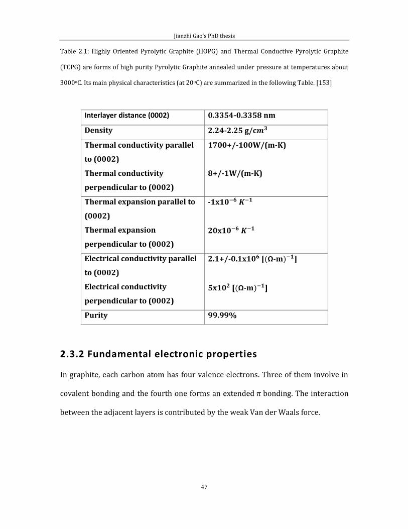
Table 2.1: Highly Oriented Pyrolytic Graphite (HOPG) and Thermal Conductive Pyrolytic Graphite
(TCPG) are forms of high purity Pyrolytic Graphite annealed under pressure at temperatures about
3000oC. Its main physical characteristics (at 20oC) are summarized in the following Table. [153]
Interlayer distance (0002) 0.3354-0.3358 nm
Density 2.24-2.25 g/c
Thermal conductivity parallel
to (0002)
Thermal conductivity
perpendicular to (0002)
1700+/-100W/(m-K)
8+/-1W/(m-K)
Thermal expansion parallel to
(0002)
Thermal expansion
perpendicular to (0002)
-1x
20x
Electrical conductivity parallel
to (0002)
Electrical conductivity
perpendicular to (0002)
2.1+/-0.1x [ Ω-m ]
5x [ Ω-m ]
Purity 99.99%
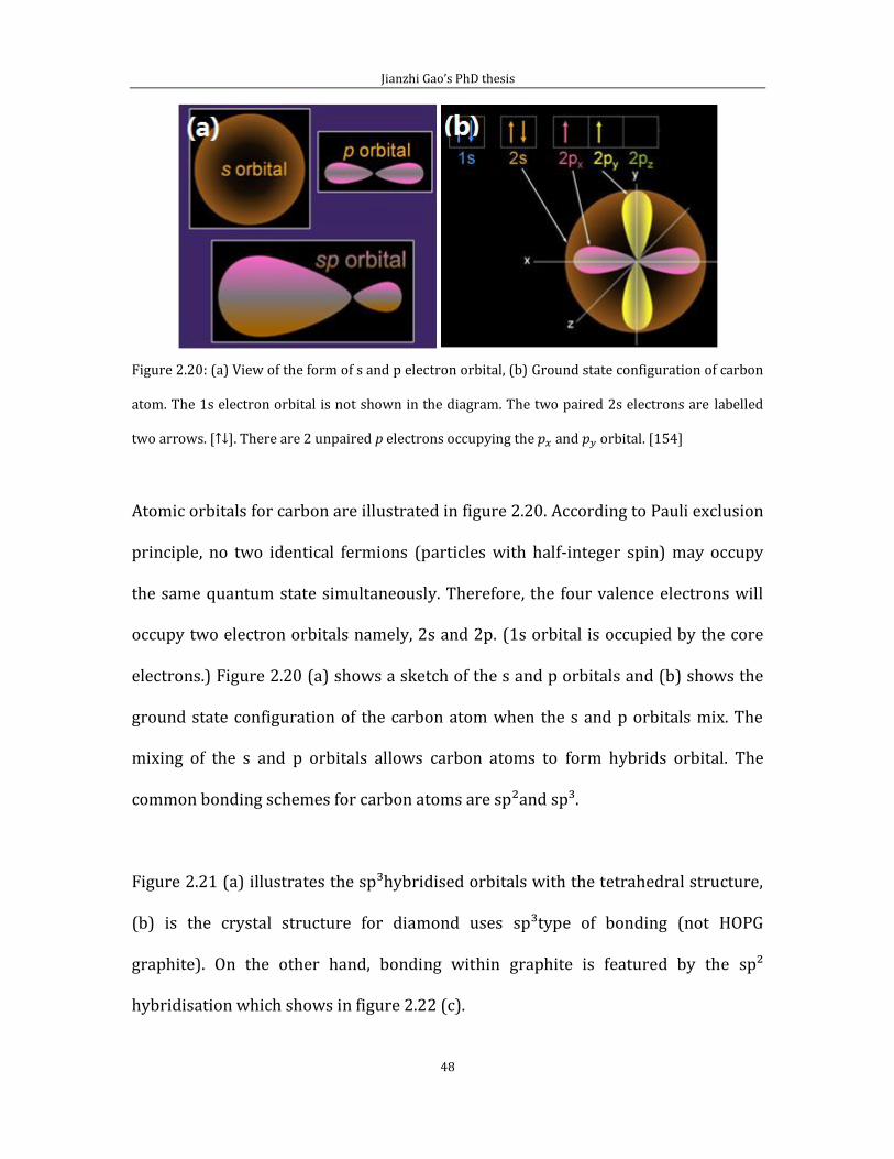
2.3.2 Fundamental electronic properties In graphite, each carbon atom has four valence electrons. Three of them involve in
covalent bonding and the fourth one forms an extended bonding. The interaction
between the adjacent layers is contributed by the weak Van der Waals force.
Jianzhi Gao’s PhD thesis
48
Figure 2.20: (a) View of the form of s and p electron orbital, (b) Ground state configuration of carbon
atom. The 1s electron orbital is not shown in the diagram. The two paired 2s electrons are labelled
two arrows. [↑↓]. There are 2 unpaired p electrons occupying the and orbital. [154]
Atomic orbitals for carbon are illustrated in figure 2.20. According to Pauli exclusion
principle, no two identical fermions (particles with half-integer spin) may occupy
the same quantum state simultaneously. Therefore, the four valence electrons will
occupy two electron orbitals namely, 2s and 2p. (1s orbital is occupied by the core
electrons.) Figure 2.20 (a) shows a sketch of the s and p orbitals and (b) shows the
ground state configuration of the carbon atom when the s and p orbitals mix. The
mixing of the s and p orbitals allows carbon atoms to form hybrids orbital. The
common bonding schemes for carbon atoms are sp²and sp³.
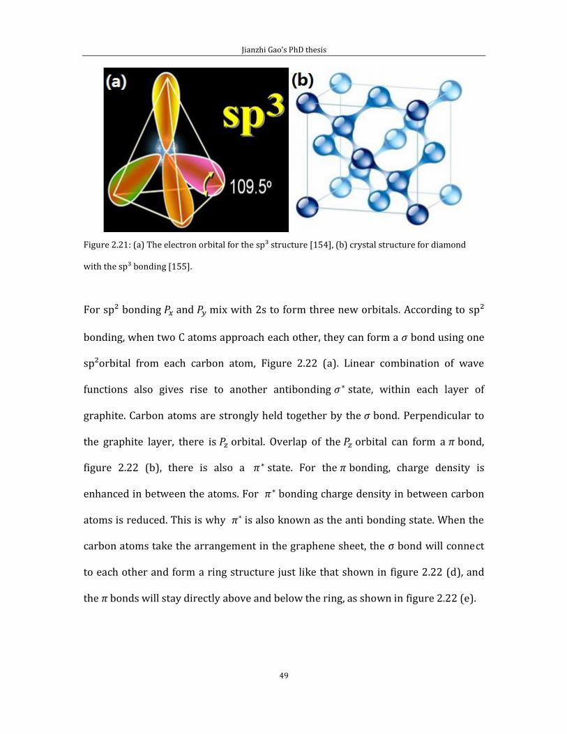
Figure 2.21 (a) illustrates the sp³hybridised orbitals with the tetrahedral structure,
(b) is the crystal structure for diamond uses sp³type of bonding (not HOPG
graphite). On the other hand, bonding within graphite is featured by the sp²
hybridisation which shows in figure 2.22 (c).
Jianzhi Gao’s PhD thesis
49
Figure 2.21: (a) The electron orbital for the sp³ structure [154], (b) crystal structure for diamond
with the sp³ bonding [155].
For sp² bonding and mix with 2s to form three new orbitals. According to sp²
bonding, when two C atoms approach each other, they can form a bond using one
sp²orbital from each carbon atom, Figure 2.22 (a). Linear combination of wave
functions also gives rise to another antibonding state, within each layer of
graphite. Carbon atoms are strongly held together by the bond. Perpendicular to
the graphite layer, there is orbital. Overlap of the orbital can form a bond,
figure 2.22 (b), there is also a state. For the bonding, charge density is
enhanced in between the atoms. For bonding charge density in between carbon
atoms is reduced. This is why * is also known as the anti bonding state. When the
carbon atoms take the arrangement in the graphene sheet, the σ bond will connect
to each other and form a ring structure just like that shown in figure 2.22 (d), and
the bonds will stay directly above and below the ring, as shown in figure 2.22 (e).
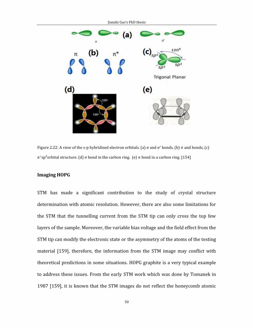
Jianzhi Gao’s PhD thesis
50
Figure 2.22: A view of the s-p hybridised electron orbitals. (a) σ and σ* bonds, (b) and bonds, (c)
sp²orbital structure. (d) σ bond in the carbon ring. (e) bond in a carbon ring. [154]
Imaging HOPG
STM has made a significant contribution to the study of crystal structure
determination with atomic resolution. However, there are also some limitations for
the STM that the tunnelling current from the STM tip can only cross the top few
layers of the sample. Moreover, the variable bias voltage and the field effect from the
STM tip can modify the electronic state or the asymmetry of the atoms of the testing
material [159], therefore, the information from the STM image may conflict with
theoretical predictions in some situations. HOPG graphite is a very typical example
to address these issues. From the early STM work which was done by Tomanek in
1987 [159], it is known that the STM images do not reflect the honeycomb atomic
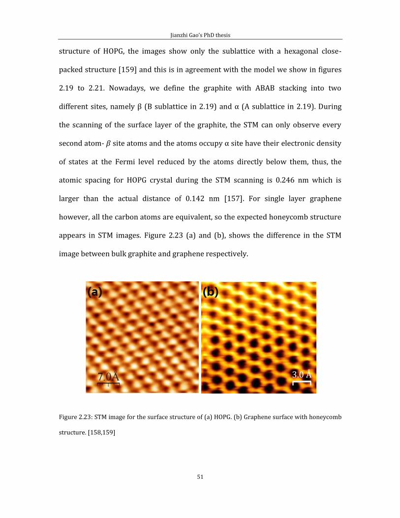
Jianzhi Gao’s PhD thesis
51
structure of HOPG, the images show only the sublattice with a hexagonal close-
packed structure [159] and this is in agreement with the model we show in figures
2.19 to 2.21. Nowadays, we define the graphite with ABAB stacking into two
different sites, namely β (B sublattice in 2.19) and α (A sublattice in 2.19). During
the scanning of the surface layer of the graphite, the STM can only observe every
second atom- site atoms and the atoms occupy α site have their electronic density
of states at the Fermi level reduced by the atoms directly below them, thus, the
atomic spacing for HOPG crystal during the STM scanning is 0.246 nm which is
larger than the actual distance of 0.142 nm [157]. For single layer graphene
however, all the carbon atoms are equivalent, so the expected honeycomb structure
appears in STM images. Figure 2.23 (a) and (b), shows the difference in the STM
image between bulk graphite and graphene respectively.
Figure 2.23: STM image for the surface structure of (a) HOPG. (b) Graphene surface with honeycomb
structure. [158,159]
3.0
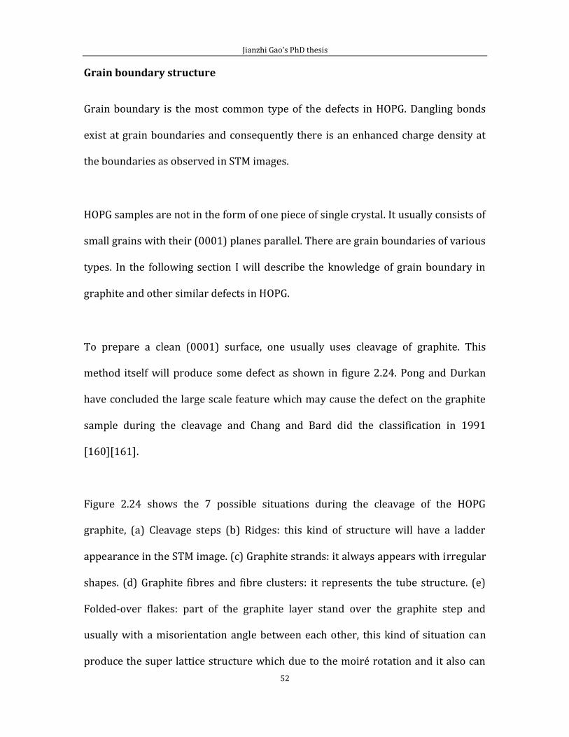
Jianzhi Gao’s PhD thesis
52
Grain boundary structure
Grain boundary is the most common type of the defects in HOPG. Dangling bonds
exist at grain boundaries and consequently there is an enhanced charge density at
the boundaries as observed in STM images.
HOPG samples are not in the form of one piece of single crystal. It usually consists of
small grains with their (0001) planes parallel. There are grain boundaries of various
types. In the following section I will describe the knowledge of grain boundary in
graphite and other similar defects in HOPG.
To prepare a clean (0001) surface, one usually uses cleavage of graphite. This
method itself will produce some defect as shown in figure 2.24. Pong and Durkan
have concluded the large scale feature which may cause the defect on the graphite
sample during the cleavage and Chang and Bard did the classification in 1991
[160][161].
Figure 2.24 shows the 7 possible situations during the cleavage of the HOPG
graphite, (a) Cleavage steps (b) Ridges: this kind of structure will have a ladder
appearance in the STM image. (c) Graphite strands: it always appears with irregular
shapes. (d) Graphite fibres and fibre clusters: it represents the tube structure. (e)
Folded-over flakes: part of the graphite layer stand over the graphite step and
usually with a misorientation angle between each other, this kind of situation can
produce the super lattice structure which due to the moiré rotation and it also can
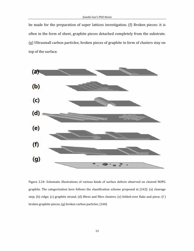
Jianzhi Gao’s PhD thesis
53
be made for the preparation of super lattices investigation. (f) Broken pieces: it is
often in the form of sheet, graphite pieces detached completely from the substrate.
(g) Ultrasmall carbon particles; broken pieces of graphite in form of clusters stay on
top of the surface.
Figure 2.24: Schematic illustrations of various kinds of surface defects observed on cleaved HOPG
graphite. The categorization here follows the classification scheme proposed in [162]: (a) cleavage
step; (b) ridge; (c) graphite strand; (d) fibres and fibre clusters; (e) folded-over flake and piece; (f )
broken graphite pieces; (g) broken carbon particles. [160]
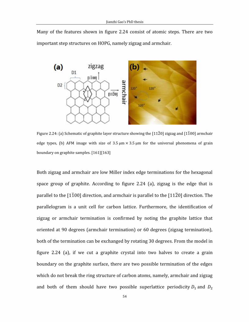
Jianzhi Gao’s PhD thesis
54
Many of the features shown in figure 2.24 consist of atomic steps. There are two
important step structures on HOPG, namely zigzag and armchair.
Figure 2.24: (a) Schematic of graphite layer structure showing the [11 0] zigzag and [1 00] armchair
edge types, (b) AFM image with size of 3.5 m 3.5 m for the universal phenomena of grain
boundary on graphite samples. [161][163]
Both zigzag and armchair are low Miller index edge terminations for the hexagonal
space group of graphite. According to figure 2.24 (a), zigzag is the edge that is
parallel to the [1 00] direction, and armchair is parallel to the [11 0] direction. The
parallelogram is a unit cell for carbon lattice. Furthermore, the identification of
zigzag or armchair termination is confirmed by noting the graphite lattice that
oriented at 90 degrees (armchair termination) or 60 degrees (zigzag termination),
both of the termination can be exchanged by rotating 30 degrees. From the model in
figure 2.24 (a), if we cut a graphite crystal into two halves to create a grain
boundary on the graphite surface, there are two possible termination of the edges
which do not break the ring structure of carbon atoms, namely, armchair and zigzag
and both of them should have two possible superlattice periodicity and
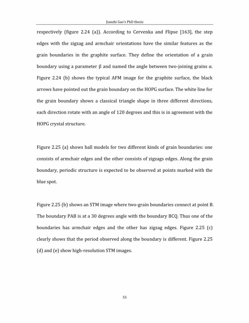
Jianzhi Gao’s PhD thesis
55
respectively (figure 2.24 (a)). According to Cervenka and Flipse [163], the step
edges with the zigzag and armchair orientations have the similar features as the
grain boundaries in the graphite surface. They define the orientation of a grain
boundary using a parameter β and named the angle between two-joining grains α.
Figure 2.24 (b) shows the typical AFM image for the graphite surface, the black
arrows have pointed out the grain boundary on the HOPG surface. The white line for
the grain boundary shows a classical triangle shape in three different directions,
each direction rotate with an angle of 120 degrees and this is in agreement with the
HOPG crystal structure.
Figure 2.25 (a) shows ball models for two different kinds of grain boundaries: one
consists of armchair edges and the other consists of zigzags edges. Along the grain
boundary, periodic structure is expected to be observed at points marked with the
blue spot.
Figure 2.25 (b) shows an STM image where two-grain boundaries connect at point B.
The boundary PAB is at a 30 degrees angle with the boundary BCQ. Thus one of the
boundaries has armchair edges and the other has zigzag edges. Figure 2.25 (c)
clearly shows that the period observed along the boundary is different. Figure 2.25
(d) and (e) show high-resolution STM images.
Jianzhi Gao’s PhD thesis
56
Figure 2.25: (a) Schematic diagrams of grain boundaries in graphite showing two possible
superlattice periodicities. Left side has D1 periodicity and right side has D2 periodicity, this model is
built based on the STM observations in figure 2.25 (d) and (e). (b) STM image of a grain boundary
containing two periodicities D1=2.18 nm and D2=3.83 nm. Scanning parameters: 50 nm 50 nm, U =
1 V, and I = 0.1 nA. (c) Cross section over the grain boundary in (b) the line ABC. (d) STM image for
the grain boundary on HOPG with D1=1.25nm, and , (e) STM image for the grain
boundary on HOPG surface with D2=0.83 nm, and . [163][164]
1nm 1nm
Jianzhi Gao’s PhD thesis
57
In each case the surface lattice of graphite is resolved and hence the orientation of
one grain relative to the other across a boundary can be determined. In figure 2.25
(d) the two grains are rotated relative to each other by 12 degrees. In figure 2.25 (e)
the two grain are rotated by 18 degrees relative to each other.
Graphite superlattices
Superlattices are often found during the STM scanning of HOPG. Graphite
superlattices usually have periodic structures with a hexagonal symmetry. Many
reasons for the formation of superlatties have been considered. These include:
physical surface deformations, dislocations, adsorption of impurities, grain
boundary, Moiré rotation patterns and point defect at the graphite surface.
Figure 2.26: STM image (a) 160 nm 160 nm showing a suprtlattice structure on graphite surface. (b)
An STM image (17 nm 17 nm) on a graphite superlattice with a periodicity of 3.8 nm. The hexagon
shows a unit cell of the superlattice. [165]
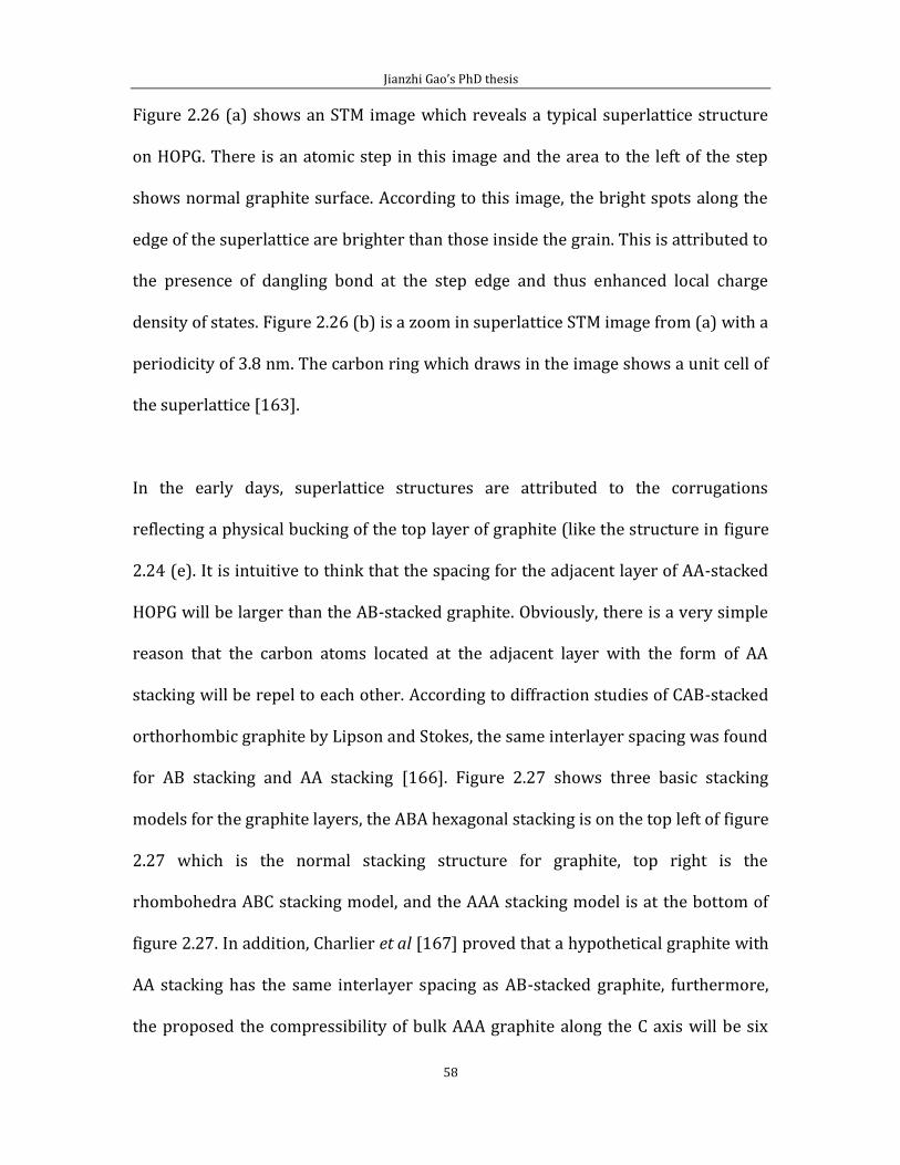
Jianzhi Gao’s PhD thesis
58
Figure 2.26 (a) shows an STM image which reveals a typical superlattice structure
on HOPG. There is an atomic step in this image and the area to the left of the step
shows normal graphite surface. According to this image, the bright spots along the
edge of the superlattice are brighter than those inside the grain. This is attributed to
the presence of dangling bond at the step edge and thus enhanced local charge
density of states. Figure 2.26 (b) is a zoom in superlattice STM image from (a) with a
periodicity of 3.8 nm. The carbon ring which draws in the image shows a unit cell of
the superlattice [163].
In the early days, superlattice structures are attributed to the corrugations
reflecting a physical bucking of the top layer of graphite (like the structure in figure
2.24 (e). It is intuitive to think that the spacing for the adjacent layer of AA-stacked
HOPG will be larger than the AB-stacked graphite. Obviously, there is a very simple
reason that the carbon atoms located at the adjacent layer with the form of AA
stacking will be repel to each other. According to diffraction studies of CAB-stacked
orthorhombic graphite by Lipson and Stokes, the same interlayer spacing was found
for AB stacking and AA stacking [166]. Figure 2.27 shows three basic stacking
models for the graphite layers, the ABA hexagonal stacking is on the top left of figure
2.27 which is the normal stacking structure for graphite, top right is the
rhombohedra ABC stacking model, and the AAA stacking model is at the bottom of
figure 2.27. In addition, Charlier et al [167] proved that a hypothetical graphite with
AA stacking has the same interlayer spacing as AB-stacked graphite, furthermore,
the proposed the compressibility of bulk AAA graphite along the C axis will be six
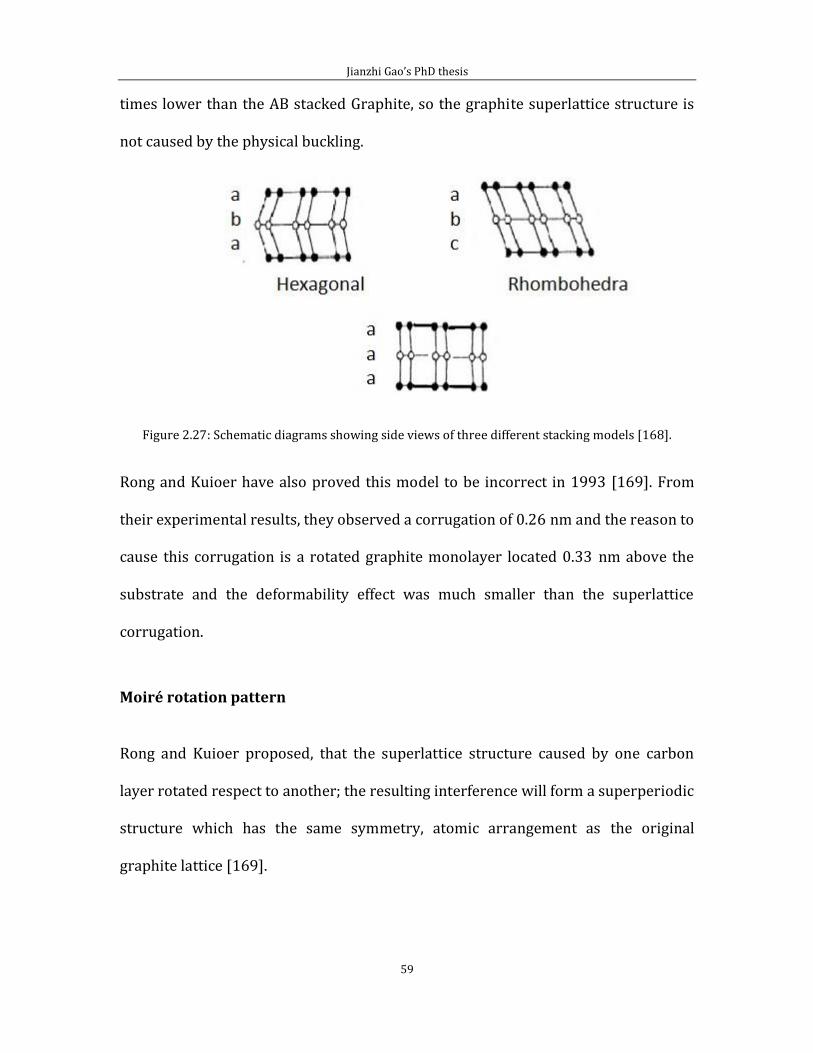
Jianzhi Gao’s PhD thesis
59
times lower than the AB stacked Graphite, so the graphite superlattice structure is
not caused by the physical buckling.
Figure 2.27: Schematic diagrams showing side views of three different stacking models [168].
Rong and Kuioer have also proved this model to be incorrect in 1993 [169]. From
their experimental results, they observed a corrugation of 0.26 nm and the reason to
cause this corrugation is a rotated graphite monolayer located 0.33 nm above the
substrate and the deformability effect was much smaller than the superlattice
corrugation.
Moiré rotation pattern
Rong and Kuioer proposed, that the superlattice structure caused by one carbon
layer rotated respect to another; the resulting interference will form a superperiodic
structure which has the same symmetry, atomic arrangement as the original
graphite lattice [169].
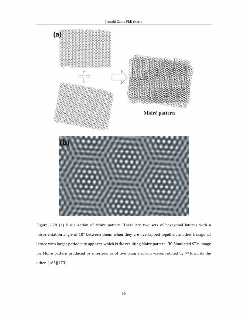
Jianzhi Gao’s PhD thesis
60
Figure 2.28 (a) Visualization of Moire pattern. There are two sets of hexagonal lattices with a
misorientation angle of 10° between them; when they are overlapped together, another hexagonal
lattice with larger periodicity appears, which is the resulting Moire pattern. (b) Simulated STM image
for Moire pattern produced by interference of two plain electron waves rotated by 7o towards the
other. [165][173]
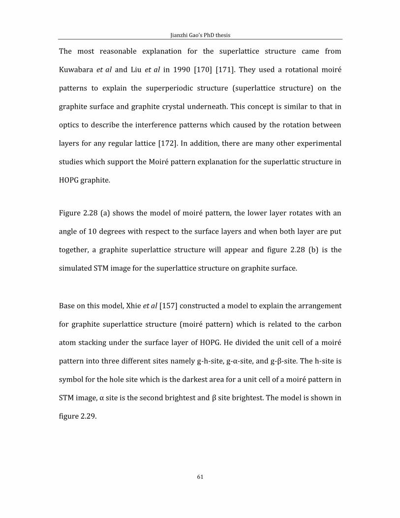
Jianzhi Gao’s PhD thesis
61
The most reasonable explanation for the superlattice structure came from
Kuwabara et al and Liu et al in 1990 [170] [171]. They used a rotational moiré
patterns to explain the superperiodic structure (superlattice structure) on the
graphite surface and graphite crystal underneath. This concept is similar to that in
optics to describe the interference patterns which caused by the rotation between
layers for any regular lattice [172]. In addition, there are many other experimental
studies which support the Moiré pattern explanation for the superlattic structure in
HOPG graphite.
Figure 2.28 (a) shows the model of moiré pattern, the lower layer rotates with an
angle of 10 degrees with respect to the surface layers and when both layer are put
together, a graphite superlattice structure will appear and figure 2.28 (b) is the
simulated STM image for the superlattice structure on graphite surface.
Base on this model, Xhie et al [157] constructed a model to explain the arrangement
for graphite superlattice structure (moiré pattern) which is related to the carbon
atom stacking under the surface layer of HOPG. He divided the unit cell of a moiré
pattern into three different sites namely g-h-site, g-α-site, and g-β-site. The h-site is
symbol for the hole site which is the darkest area for a unit cell of a moiré pattern in
STM image, α site is the second brightest and β site brightest. The model is shown in
figure 2.29.
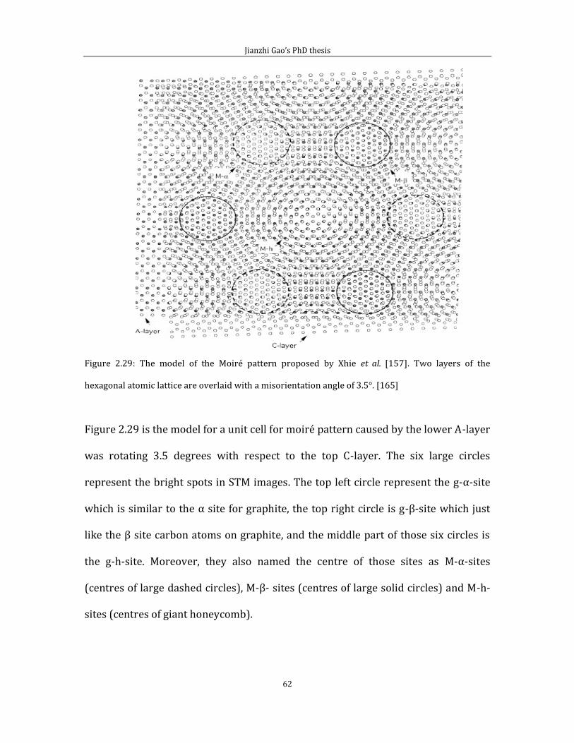
Jianzhi Gao’s PhD thesis
62
Figure 2.29: The model of the Moiré pattern proposed by Xhie et al. [157]. Two layers of the
hexagonal atomic lattice are overlaid with a misorientation angle of 3.5°. [165]
Figure 2.29 is the model for a unit cell for moiré pattern caused by the lower A-layer
was rotating 3.5 degrees with respect to the top C-layer. The six large circles
represent the bright spots in STM images. The top left circle represent the g-α-site
which is similar to the α site for graphite, the top right circle is g-β-site which just
like the β site carbon atoms on graphite, and the middle part of those six circles is
the g-h-site. Moreover, they also named the centre of those sites as M-α-sites
(centres of large dashed circles), M-β- sites (centres of large solid circles) and M-h-
sites (centres of giant honeycomb).
Jianzhi Gao’s PhD thesis
63
The stacking mode for normal graphite is ABAB… with a form of honeycomb, when a
twist boundary appears, the original ABAB… stacking of graphite will distort to
CABAB… stacking. Moreover, the dislocation between the top layer and second layer
will induce superstructure moiré pattern under the scanning of STM. According to
this situation, two different types of circles will appear in a honeycomb-like ring,
large solid circles (top right circle in figure 2.29) and large dashed circles (top left
circle in figure 2.29) and both of them with different regions and atomic
arrangements. In the large solid circles each α site atom of the graphite at the top C
layer has an atom directly below and locate at second A layer, whereas in the large
dashed circles, each β site atom in the A layer has an atom partially above it. Under
this atomic arrangement, the original carbon atom sublattice will form the large
solid circles and the large dashed circles separately; hence the STM images will
reflect the hexagonal lattices for the moiré pattern or the graphite superlattice
structure.
Earlier, we have discussed the reason for the STM image showing the close-packed
atomic arrangement on graphite surface with different brightness. However, for the
superlattice the situation is much more complicated. When the stacking form
changed from ABAB… to CABAB…, the atoms in the top layer can be at any site
above the second layer. Xhie et al support an assumption that the carbon atoms at
the C layer which above a hole site in A (second layer) layer (carbon atoms at C layer
do not have an atom directly below) will show the maximum intensity in the STM
images, just like the atoms from the β sublattice in ABAB stacked graphite.
Jianzhi Gao’s PhD thesis
64
According to this, the C layer carbon atoms above the original α site in the A layer
will show lower intensity. Finally, the atom above an original β site in the second
layer appears with the minimum intensity. Comparing this assumption with the STM
images, for an M-h-site, atoms at the C layer will have the choices of occupying
either the α or the β site at the A layer. Atoms above the α sites will be brighter in
the STM images, which is due to the lower density. In an M-α-site or an M-β-site, the
atom at the C layer will sit above a hole site or β/α site, and the atom on the hole site
will look brighter. From this deduction, the M-β-sites in the moiré pattern will show
the brightest point in STM images when the atom above the α or hole sites in the
second layer, hence the atoms at the M-β-sites have the higher electronic density of
state and M-α-sits will be second brightest, M-h-site third. From this analysis, M-β-
sites should be the peaks of the superlattices and M-α-sits must be the valleys of the
superlattices and M-h-sites are the holes of the superlattices.
2.3.3 Point defects created by ion bombardment
Point defect is another kind of defect on the HOPG surface. This kind of defect affects
the physical and chemical properties of the area surrounding the defect. In contrast
to grain boundaries and atomic steps, point defects are not abundant on HOPG
surface and hence not easily found with the STM which images a small area only.
However, point defect can be created by bombardment with energetic ions. Ions of
inert gas molecules are commonly used for generating defects on HOPG. As well as
creating defects, the incoming ions can be trapped by the graphite lattice as shown
by the work of Choi, Kim and Kang [174]. In 1992, Choi, Kim and Kang studied
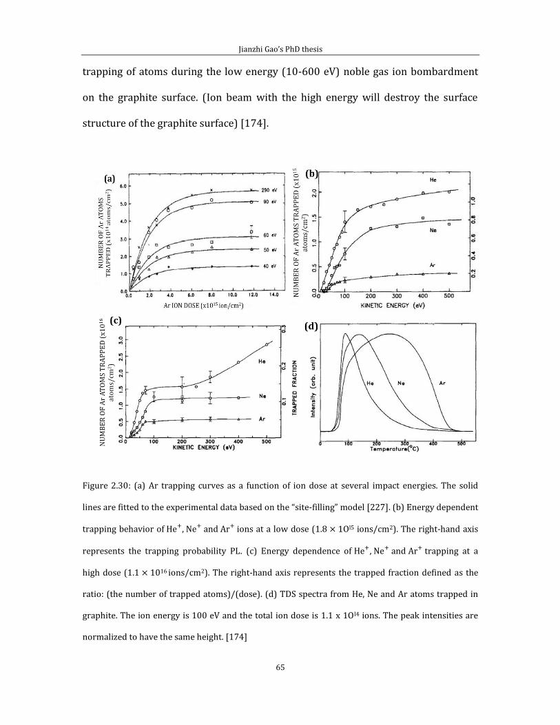
Jianzhi Gao’s PhD thesis
65
trapping of atoms during the low energy (10-600 eV) noble gas ion bombardment
on the graphite surface. (Ion beam with the high energy will destroy the surface
structure of the graphite surface) [174].
Figure 2.30: (a) Ar trapping curves as a function of ion dose at several impact energies. The solid
lines are fitted to the experimental data based on the “site-filling” model [227]. (b) Energy dependent
trapping behavior of e , e and Ar ions at a low dose (1.8 1Ol5 ions/cm2). The right-hand axis
represents the trapping probability PL. (c) Energy dependence of e , e and Ar trapping at a
high dose (1.1 1016 ions/cm2). The right-hand axis represents the trapped fraction defined as the
ratio: (the number of trapped atoms)/(dose). (d) TDS spectra from He, Ne and Ar atoms trapped in
graphite. The ion energy is 100 eV and the total ion dose is 1.1 x 1Ol4 ions. The peak intensities are
normalized to have the same height. [174]
Jianzhi Gao’s PhD thesis
66
Figure 2.30 (a) shows the dose dependence of Ar trapping at different energies
incident, ranging from 40 to 290 eV. The number of trapped atoms increases with
the beam energy and saturated in the higher dose. For the comparison, Choi, Kim
and Kang used He, Ne, and Ar ion with energy ranging from 1 eV to 500 eV and
under both low and higher dose of 1.8 1Ol5 ions/cm2 and 1.1 1016 ions/cm2
respectively. There are several interesting features to be pointed out, according to
figure 2.30 (b), the magnitude of is in order of (He)> (Ne)> (Ar) at the
whole energy range. In addition, increase dramatically in the energy region
between 10 eV to100 eV, then slow down at the kinetic energy larger than 100 eV.
The trapping threshold is found between the 10 eV to 30 eV. The trapping threshold
is He< Ne<Ar. The TDS spectra from the trapped He, Ne and Ar atoms are shown in
figure 2.30 (d), the desorption temperature of those three molecules are in the order
of He (90-100 0C)< Ne(120-160 0C)<Ar(200 -300 0C).
Ion bombardment is a controllable process in which one can change the kinetic
energy of the ions and the flux of ions independently. For inert gas ions, there is
further the advantage that they do not chemically react with HOPG. As far as the
defect created by ion bombardment, there are several types as illustrated in Figure
2.31.
i) Single vacancies: one carbon atom missing from the graphite lattice;
ii) Interstitial defect: ion or atom trapped in the space of graphite layer;
iii) Stone Wales defect: Re-bonding of carbon atoms due to a missing carbon atom.
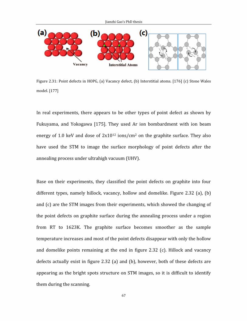
Jianzhi Gao’s PhD thesis
67
Figure 2.31: Point defects in HOPG, (a) Vacancy defect, (b) Interstitial atoms. [176] (c) Stone Wales
model. [177]
In real experiments, there appears to be other types of point defect as shown by
Fukuyama, and Yokogawa [175]. They used Ar ion bombardment with ion beam
energy of 1.0 keV and dose of 2x10¹² ions/cm2 on the graphite surface. They also
have used the STM to image the surface morphology of point defects after the
annealing process under ultrahigh vacuum (UHV).
Base on their experiments, they classified the point defects on graphite into four
different types, namely hillock, vacancy, hollow and domelike. Figure 2.32 (a), (b)
and (c) are the STM images from their experiments, which showed the changing of
the point defects on graphite surface during the annealing process under a region
from RT to 1623K. The graphite surface becomes smoother as the sample
temperature increases and most of the point defects disappear with only the hollow
and domelike points remaining at the end in figure 2.32 (c). Hillock and vacancy
defects actually exist in figure 2.32 (a) and (b), however, both of these defects are
appearing as the bright spots structure on STM images, so it is difficult to identify
them during the scanning.
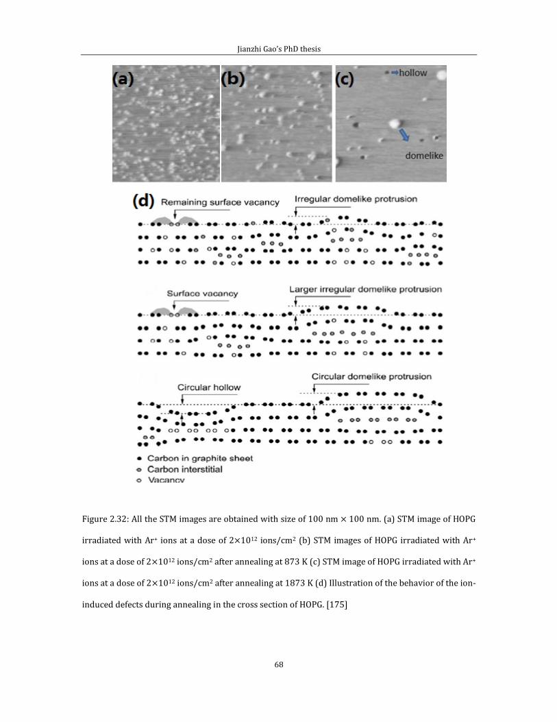
Jianzhi Gao’s PhD thesis
68
Figure 2.32: All the STM images are obtained with size of 100 nm 100 nm. (a) STM image of HOPG
irradiated with Ar+ ions at a dose of 2 1012 ions/cm2 (b) STM images of HOPG irradiated with Ar+
ions at a dose of 2 1012 ions/cm2 after annealing at 873 K (c) STM image of HOPG irradiated with Ar+
ions at a dose of 2 1012 ions/cm2 after annealing at 1873 K (d) Illustration of the behavior of the ion-
induced defects during annealing in the cross section of HOPG. [175]
Jianzhi Gao’s PhD thesis
69
Fukuyama and Yokogawa proposed a model to explain the response of different
defects to temperature as shown in figure 2.32 (d). Actually, there are many
scattered carbon atoms at the graphite surface and in the space between the
graphite layers after sputtering to form the hilliock point defects and vacancy
defects. When the sample temperature increases, it will enhance diffusion of the
scattered carbon atoms hence those carbon atoms will move and search the suitable
site to stay. Moreover, the scattered carbon atoms will fill into the vacancy and
recombine to each other and try to form the original surface structure, therefore,
there will be empty site at the lower graphite layer, and become the hollow defects
at the end. On another aspect, the carbon atoms from the small hillock, tend to join
bigger hillock defects and form a dish-like structured between two graphite layers.
This gives rise to the domelike defect. From that information, we can have a basic
understanding for different types of point defects which are created by ion
bombardment. Furthermore, there are also more valuable field for the point defect
structure, such as the vacancy magnetism under the lower temperature, self energy
of the point defect structure, electronic properties of the point defect superlattice
structure and saturated by different atoms. (Nitrogen doping will be discussed in
the results section.). From the recent works, there are some new phenomena
discovered on the HOPG surface by the scanning tunnelling microscope which
cannot be fully understood, such as wavy defect on graphite/graphene surface
[160,178], and those defect structures are still need to characterized. Consequently,
it is important to understanding those defect structures and their electronic
properties to provide a platform for the further applications of carbon materials.
Jianzhi Gao’s PhD thesis
70
Chapter 3 Experimental techniques and methodology
3.1 Surface analysis methods In the field of surface science, the definition of a surface can be understood as a
transition region between the outside media, or vacuum, and the uniform bulk
material [179]. In this transition region, the chemical and physical properties of the
materials are very different from that of the bulk, due to different electronic
structure and atomic structure. Surface properties are very important in making
biosensors, solar cells, microelectronic devices, and in catalysis. Therefore, there is a
great demand for the investigation of surface properties, and hence the
development of surface characterizing techniques.
A number of surface science techniques are listed in table 3.1. Some of these listed
techniques have been applied to study alkanethiol self-assembled monolayers and
characterisation of graphite surfaces. Most of my PhD research involves surface
imaging with the STM. Therefore, I will focus on the description of STM and related
methods.
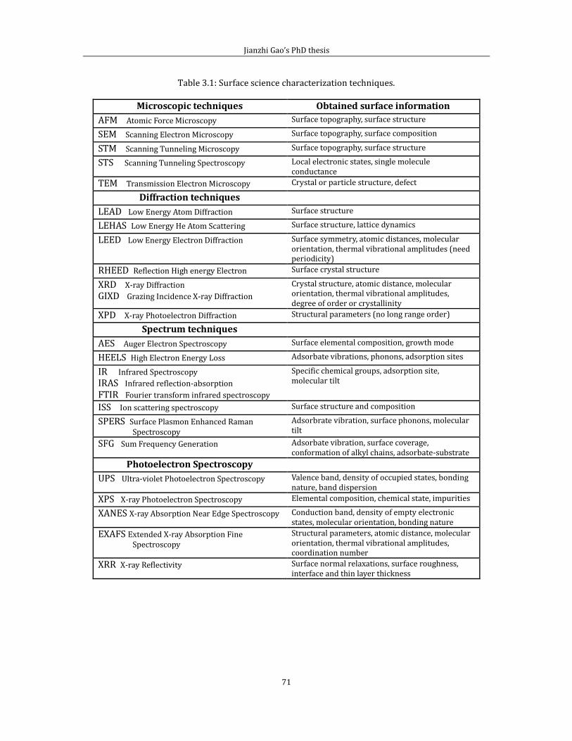
Jianzhi Gao’s PhD thesis
71
Table 3.1: Surface science characterization techniques.
Microscopic techniques Obtained surface information
AFM Atomic Force Microscopy Surface topography, surface structure
SEM Scanning Electron Microscopy Surface topography, surface composition
STM Scanning Tunneling Microscopy Surface topography, surface structure
STS Scanning Tunneling Spectroscopy Local electronic states, single molecule conductance
TEM Transmission Electron Microscopy Crystal or particle structure, defect
Diffraction techniques
LEAD Low Energy Atom Diffraction Surface structure
LEHAS Low Energy He Atom Scattering Surface structure, lattice dynamics
LEED Low Energy Electron Diffraction Surface symmetry, atomic distances, molecular orientation, thermal vibrational amplitudes (need periodicity)
RHEED Reflection High energy Electron Surface crystal structure
XRD X-ray Diffraction
GIXD Grazing Incidence X-ray Diffraction
Crystal structure, atomic distance, molecular orientation, thermal vibrational amplitudes, degree of order or crystallinity
XPD X-ray Photoelectron Diffraction Structural parameters (no long range order)
Spectrum techniques
AES Auger Electron Spectroscopy Surface elemental composition, growth mode
HEELS High Electron Energy Loss Adsorbate vibrations, phonons, adsorption sites
IR Infrared Spectroscopy
IRAS Infrared reflection-absorption
FTIR Fourier transform infrared spectroscopy
Specific chemical groups, adsorption site, molecular tilt
ISS Ion scattering spectroscopy Surface structure and composition
SPERS Surface Plasmon Enhanced Raman Spectroscopy
Adsorbrate vibration, surface phonons, molecular tilt
SFG Sum Frequency Generation Adsorbate vibration, surface coverage, conformation of alkyl chains, adsorbate-substrate
Photoelectron Spectroscopy
UPS Ultra-violet Photoelectron Spectroscopy Valence band, density of occupied states, bonding nature, band dispersion
XPS X-ray Photoelectron Spectroscopy Elemental composition, chemical state, impurities
XANES X-ray Absorption Near Edge Spectroscopy Conduction band, density of empty electronic states, molecular orientation, bonding nature
EXAFS Extended X-ray Absorption Fine Spectroscopy
Structural parameters, atomic distance, molecular orientation, thermal vibrational amplitudes, coordination number
XRR X-ray Reflectivity Surface normal relaxations, surface roughness, interface and thin layer thickness
Jianzhi Gao’s PhD thesis
72
3.2 Scanning Tunnelling Microscopy Scanning tunnelling microscopy is a relatively new and powerful experimental
technique for investigation of surface structures. It was invented by Binnig, Rohrer
and co-workers at the IBM Zurich Research Laboratory in 1981 [180,181], to
achieve real-space atomic resolution imaging of solid surfaces. Binnig and Rohrer
were awarded the Nobel Prize in Physics in 1986. Since then a number of related
surface imaging methods have been developed based on the fundamental concept of
the STM. Among them are: atomic force microscopy (AFM), scanning capacitance
microscopy (SCM), magnetic force microscopy (MFM), Kelvin probe force
microscopy (KPFM), electrostatic force microscopy (EFM) and chemical force
microscopy (CFM). The most widely used are AFM and STM.
The STM measurement is obtained by detecting the tunnelling current, which can be
explained as a quantum mechanical phenomenon. The basic principle of electron
tunnelling can be demonstrated in a 1-Dimensional model, schematically shown in
figure 3.1.
According to figure 3.1, the two electrodes can be either metal or semiconductor.
They are close to each other and separated by an energy barrier. Generally, the
electrons in both electrodes are confined under their Fermi levels and the Fermi
levels are equal at equilibrium when there is no applied bias voltage, assuming they
are the same material.
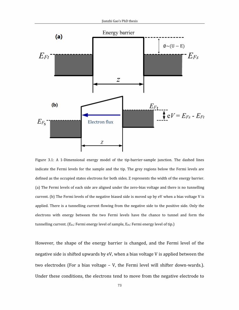
Jianzhi Gao’s PhD thesis
73
Figure 3.1: A 1-Dimensional energy model of the tip-barrier-sample junction. The dashed lines
indicate the Fermi levels for the sample and the tip. The grey regions below the Fermi levels are
defined as the occupied states electrons for both sides. Z represents the width of the energy barrier.
(a) The Fermi levels of each side are aligned under the zero-bias voltage and there is no tunnelling
current. (b) The Fermi levels of the negative biased side is moved up by eV when a bias voltage V is
applied. There is a tunnelling current flowing from the negative side to the positive side. Only the
electrons with energy between the two Fermi levels have the chance to tunnel and form the
tunnelling current. (EFs: Fermi energy level of sample, EFt: Fermi energy level of tip.)
However, the shape of the energy barrier is changed, and the Fermi level of the
negative side is shifted upwards by eV, when a bias voltage V is applied between the
two electrodes (For a bias voltage – V, the Fermi level will shifter down-wards.).
Under these conditions, the electrons tend to move from the negative electrode to
s
t
Electron flux
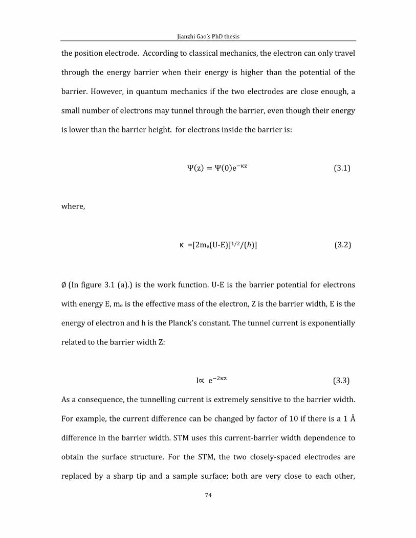
Jianzhi Gao’s PhD thesis
74
the position electrode. According to classical mechanics, the electron can only travel
through the energy barrier when their energy is higher than the potential of the
barrier. However, in quantum mechanics if the two electrodes are close enough, a
small number of electrons may tunnel through the barrier, even though their energy
is lower than the barrier height. for electrons inside the barrier is:
(3.1)
where,
κ =[2me(U-E)]1/2/(ħ)] (3.2)
(In figure 3.1 (a).) is the work function. U-E is the barrier potential for electrons
with energy E, me is the effective mass of the electron, Z is the barrier width, E is the
energy of electron and h is the Planck’s constant. The tunnel current is exponentially
related to the barrier width Z:
I (3.3)
As a consequence, the tunnelling current is extremely sensitive to the barrier width.
For example, the current difference can be changed by factor of 10 if there is a 1 Å
difference in the barrier width. STM uses this current-barrier width dependence to
obtain the surface structure. For the STM, the two closely-spaced electrodes are
replaced by a sharp tip and a sample surface; both are very close to each other,
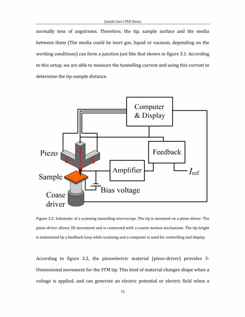
Jianzhi Gao’s PhD thesis
75
normally tens of angstroms. Therefore, the tip, sample surface and the media
between them (The media could be inert gas, liquid or vacuum, depending on the
working conditions) can form a junction just like that shown in figure 3.1. According
to this setup, we are able to measure the tunnelling current and using this current to
determine the tip-sample distance.
Figure 3.2: Schematic of a scanning tunnelling microscope. The tip is mounted on a piezo-driver. The
piezo-driver allows 3D movement and is connected with a coarse motion mechanism. The tip height
is maintained by a feedback loop while scanning and a computer is used for controlling and display.
According to figure 3.2, the piezoelectric material (piezo-driver) provides 3-
Dimensional movement for the STM tip. This kind of material changes shape when a
voltage is applied, and can generate an electric potential or electric field when a
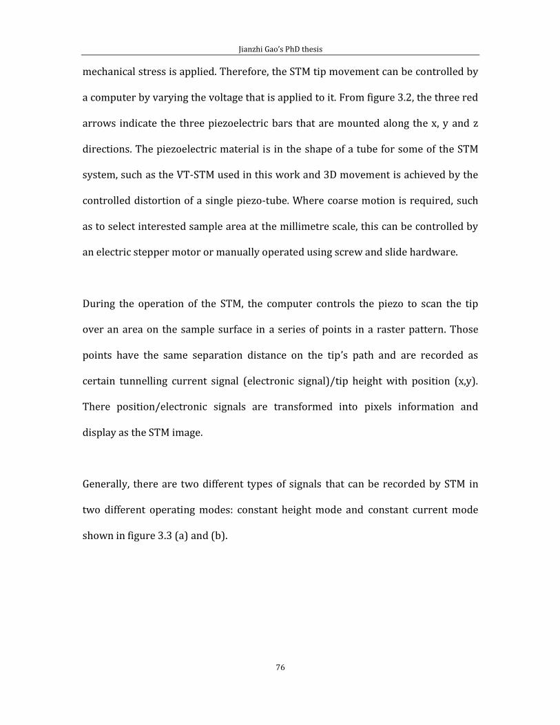
Jianzhi Gao’s PhD thesis
76
mechanical stress is applied. Therefore, the STM tip movement can be controlled by
a computer by varying the voltage that is applied to it. From figure 3.2, the three red
arrows indicate the three piezoelectric bars that are mounted along the x, y and z
directions. The piezoelectric material is in the shape of a tube for some of the STM
system, such as the VT-STM used in this work and 3D movement is achieved by the
controlled distortion of a single piezo-tube. Where coarse motion is required, such
as to select interested sample area at the millimetre scale, this can be controlled by
an electric stepper motor or manually operated using screw and slide hardware.
During the operation of the STM, the computer controls the piezo to scan the tip
over an area on the sample surface in a series of points in a raster pattern. Those
points have the same separation distance on the tip’s path and are recorded as
certain tunnelling current signal (electronic signal)/tip height with position (x,y).
There position/electronic signals are transformed into pixels information and
display as the STM image.
Generally, there are two different types of signals that can be recorded by STM in
two different operating modes: constant height mode and constant current mode
shown in figure 3.3 (a) and (b).
Jianzhi Gao’s PhD thesis
77
Figure 3.3: Schematic of two working modes of the STM. (a) Constant current mode where the STM
tip height is adjusted during scanning by keeping the tunnelling current fixed, The different tip
heights at each position are recorded to construct the image. (b) Constant height mode, the tip height
is constant during the scanning, and the different tunnelling current values are recorded.
In constant current mode in (a), a feedback circuit is employed to change the tip
height and keep the tunnelling current at the pre-set value. The variation of tip-
sample distance z causes the adjustment in the tunnelling current when the STM tip
meets the surface structure. From the detected variable tunnelling current, the
feedback circuit can adjust the voltage applied in the z direction of piezo, hence
changing the tip height until the tunnelling current returns to the pre-set value. The
tip height is recorded as the position information by the computer. As all of
positions information is recorded, they are displayed in a STM image, and the
contrast differences represent the different local charge density of state at each
position of the scanned area.
Jianzhi Gao’s PhD thesis
78
Constant height mode is operated by using the constant feedback to keep the tip at
a fixed height during the scanning. During the scanning, the surface corrugation
results in variation in different tip-sample distance z and causes different tunnelling
current values at each position. Computer records this relative tunnelling current
value from point to point, which displays as different contrasts in STM image. The
constant height mode does not require time to adjust the tip height during the
scanning; therefore, the scanning speed can be very high. As the tip height is fixed,
the STM tip can be easily crashed if there are some unexpected high structure on the
scanning area. Hence, the constant current mode is preferred to use to study a
surface at first and then the constant height mode can be used to observe surface
features for atomically flat regions.
The main experimental instrument used in this research is the Omicron variable
temperature STM (VT-STM).
3.3 VT-STM
Our VT-STM is mounted on an ultra high vacuum (UHV) system, which has a base
vacuum level of 2x mbar. The vacuum is maintained by an ion pump and a
titanium sublimation pump. In addition to the VT-STM, we also have two
evaporation sources, LEED optics, a sputtering ion gun, and a quadrupole mass
spectrometer for residual gas analysis. There is a turbo pump for evacuating the gas
line and another turbo pump for evacuating the main STM chamber.
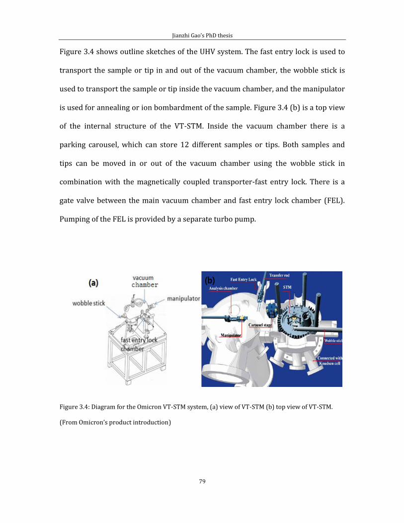
Jianzhi Gao’s PhD thesis
79
Figure 3.4 shows outline sketches of the UHV system. The fast entry lock is used to
transport the sample or tip in and out of the vacuum chamber, the wobble stick is
used to transport the sample or tip inside the vacuum chamber, and the manipulator
is used for annealing or ion bombardment of the sample. Figure 3.4 (b) is a top view
of the internal structure of the VT-STM. Inside the vacuum chamber there is a
parking carousel, which can store 12 different samples or tips. Both samples and
tips can be moved in or out of the vacuum chamber using the wobble stick in
combination with the magnetically coupled transporter-fast entry lock. There is a
gate valve between the main vacuum chamber and fast entry lock chamber (FEL).
Pumping of the FEL is provided by a separate turbo pump.
Figure 3.4: Diagram for the Omicron VT-STM system, (a) view of VT-STM (b) top view of VT-STM.
(From Omicron’s product introduction)
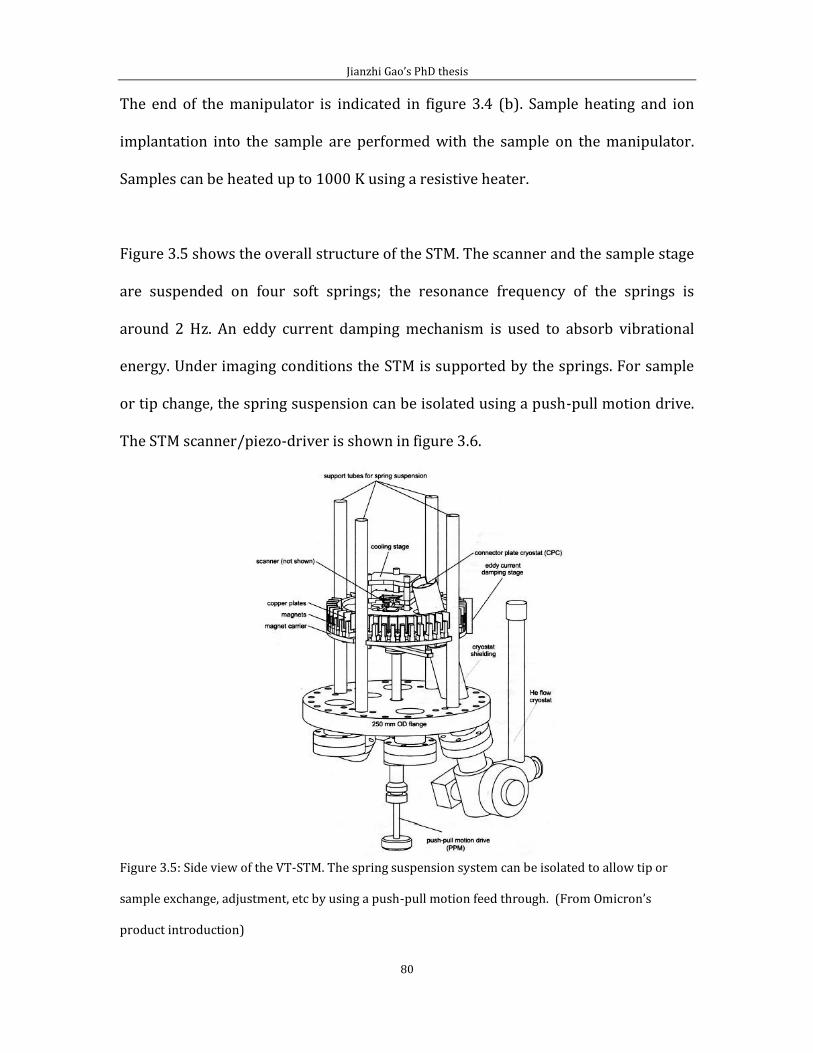
Jianzhi Gao’s PhD thesis
80
The end of the manipulator is indicated in figure 3.4 (b). Sample heating and ion
implantation into the sample are performed with the sample on the manipulator.
Samples can be heated up to 1000 K using a resistive heater.
Figure 3.5 shows the overall structure of the STM. The scanner and the sample stage
are suspended on four soft springs; the resonance frequency of the springs is
around 2 Hz. An eddy current damping mechanism is used to absorb vibrational
energy. Under imaging conditions the STM is supported by the springs. For sample
or tip change, the spring suspension can be isolated using a push-pull motion drive.
The STM scanner/piezo-driver is shown in figure 3.6.
Figure 3.5: Side view of the VT-STM. The spring suspension system can be isolated to allow tip or
sample exchange, adjustment, etc by using a push-pull motion feed through. (From Omicron’s
product introduction)
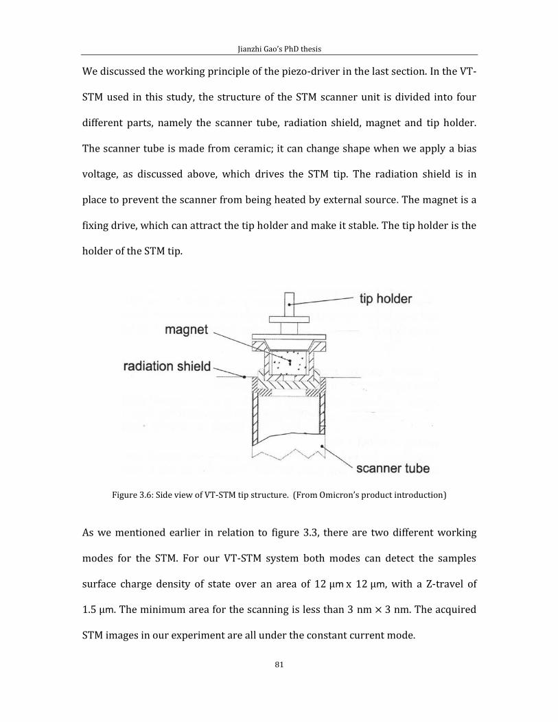
Jianzhi Gao’s PhD thesis
81
We discussed the working principle of the piezo-driver in the last section. In the VT-
STM used in this study, the structure of the STM scanner unit is divided into four
different parts, namely the scanner tube, radiation shield, magnet and tip holder.
The scanner tube is made from ceramic; it can change shape when we apply a bias
voltage, as discussed above, which drives the STM tip. The radiation shield is in
place to prevent the scanner from being heated by external source. The magnet is a
fixing drive, which can attract the tip holder and make it stable. The tip holder is the
holder of the STM tip.
Figure 3.6: Side view of VT-STM tip structure. (From Omicron’s product introduction)
As we mentioned earlier in relation to figure 3.3, there are two different working
modes for the STM. For our VT-STM system both modes can detect the samples
surface charge density of state over an area of 12 μ x 12 μ , with a Z-travel of
1.5 μ . The minimum area for the scanning is less than 3 nm 3 nm. The acquired
STM images in our experiment are all under the constant current mode.
Jianzhi Gao’s PhD thesis
82
The VT-STM, can image in a temperature range from 44 K to 1500 K, using separate
heating and cooling techniques as required. For cooling, there is a helium flow
cryostat mounted on the base plate, connected to a tank. The cooling system can
decrease the cryostat temperature down to as low as 17 K, when there is a liquid He
flows through the cryostat. There is a gas flow control block that is used for
controlling the He flow. There is a resistant heater mounted inside the cryostat and
controlled by a Lakeshore temperature controller that can adjust the cryostat
temperature between 17 K and room temperature. Moreover, the difference of the
cooling block before and during the cooling process is shown in figure 3.7 (c) and
(d).
For heating; there is a thermal exchanger projected through the base plate and
connected to the He flow cryostat. The thermal exchanger, is connected to the
cryostat by a connecter plate that is mounted on the cooling stage using highly
flexible copper braids. In addition, the highly flexible copper braids can also be used
to minimize vibration during low temperature STM scanning. To operate the cooling
progress, the cooling block needs to be moved to cover the top of the sample holder,
shown in figure 3.7 (a), to achieve the thermal contact and cool the sample, shown in
figure 3.7 (b). However, for our experiment; we do not require the sample
temperature as low as that of liquid He, therefore, we use liquid Nitrogen instead.
For raising the sample temperature, there are two possible methods, namely, direct
heating and radiative heating. In both cases there is a DC current required. For
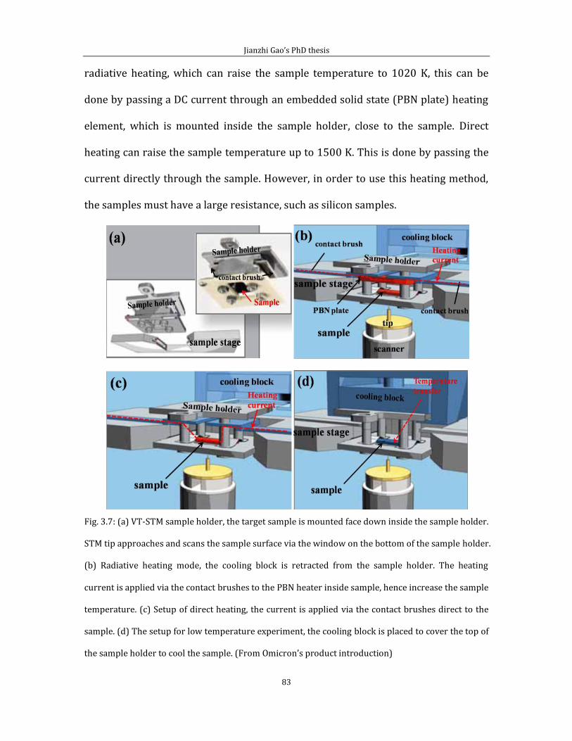
Jianzhi Gao’s PhD thesis
83
radiative heating, which can raise the sample temperature to 1020 K, this can be
done by passing a DC current through an embedded solid state (PBN plate) heating
element, which is mounted inside the sample holder, close to the sample. Direct
heating can raise the sample temperature up to 1500 K. This is done by passing the
current directly through the sample. However, in order to use this heating method,
the samples must have a large resistance, such as silicon samples.
Fig. 3.7: (a) VT-STM sample holder, the target sample is mounted face down inside the sample holder.
STM tip approaches and scans the sample surface via the window on the bottom of the sample holder.
(b) Radiative heating mode, the cooling block is retracted from the sample holder. The heating
current is applied via the contact brushes to the PBN heater inside sample, hence increase the sample
temperature. (c) Setup of direct heating, the current is applied via the contact brushes direct to the
sample. (d) The setup for low temperature experiment, the cooling block is placed to cover the top of
the sample holder to cool the sample. (From Omicron’s product introduction)

Jianzhi Gao’s PhD thesis
84
3.4 ISE 5 ion gun The ISE 5 ion gun is a cold cathode ion gun. The main purpose of this ion gun is for
sample cleaning. However, in our experiment, it plays an important role for the low
energy doping of the HOPG. The external view of the ISE 5 ion gun is shown in figure
3.8, the main components for the ion gun are high voltage feedthroughs, gas inlet
(connected to gas line), earthed cover over the ion flight tube and a removable
permanent magnet.
Figure 3.8: External view of ISE 5 ion gun. (From Omicron’s product introduction)
Ions produced by the ISE 5 ion gun can be from 250 eV to 5 keV, with a maximum beam
current up to 45 A. The beam current can be controlled by the gas flux using the leak
valve. The principle of operation of the ISE 5 ion gun is shown in figure 3.9.
Figure 3.9: Diagram of the ISE 5 ion gun. (From Omicron’s product introduction)
Jianzhi Gao’s PhD thesis
85
The gases that we have used for the ion implantation process are argon and
nitrogen, both with purity of up to 99.999%. When gas is introduced to the gas cell
of the ISE 5 ion gun it acts as the cold cathode ion source. A voltage is applied
between the anode and cathode keeping a gas discharge. The removable magnet
supplies a longitudinal magnetic field a cross the source region and resulting in a
spiral path for the electrons, enhancing electron molecule collision. The typical
discharge current is 1 mA, however, in our case, for low energy ion sputtering the
discharge current is expected to be much smaller, delivering a current density at the
sample in a range of 1 to 3 nA/c . The beam energy of the ions is relative to the
earth potential. Following the discharge process, the ions will go through an
aperture in the cathode plate into the flight tube. Inside the flight tube the ions
travel with the same energy as when they left the gun chamber. Due to the space
charge limitation, the spot size broadens at low beam energy. The focus element in
the flight tube is used to focus the ion beam onto the sample.
3.5 Sample and tip preparation
Tip preparation
Preparation of the STM tip is a significant step for all the STM experiments. The
quality of the tip can directly influence the result of the acquired STM images. The
ideal condition for an STM tip is to have only one atom at the end of the tip. We
choose tungsten as the material to make the STM tips for its high electrical
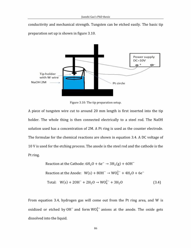
Jianzhi Gao’s PhD thesis
86
conductivity and mechanical strength. Tungsten can be etched easily. The basic tip
preparation set up is shown in figure 3.10.
Figure 3.10: The tip preparation setup.
A piece of tungsten wire cut to around 20 mm length is first inserted into the tip
holder. The whole thing is then connected electrically to a steel rod. The NaOH
solution used has a concentration of 2M. A Pt ring is used as the counter electrode.
The formulae for the chemical reactions are shown in equation 3.4. A DC voltage of
10 V is used for the etching process. The anode is the steel rod and the cathode is the
Pt ring.
Reaction at the Cathode: 2O e 3 2 g O
Reaction at the Anode: s O O 2O e
Total: s 2O 2 2O O 2 3 2O (3.4)
From equation 3.4, hydrogen gas will come out from the Pt ring area, and W is
oxidized or etched by O and form O anions at the anode. The oxide gets
dissolved into the liquid.
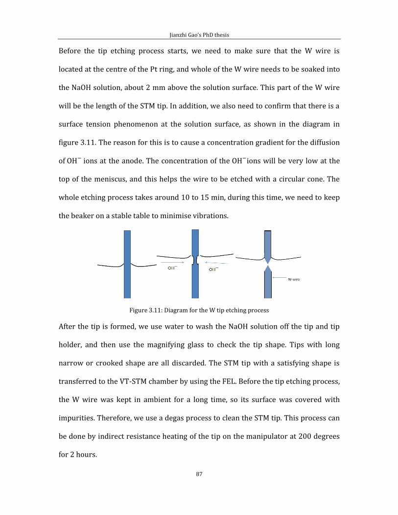
Jianzhi Gao’s PhD thesis
87
Before the tip etching process starts, we need to make sure that the W wire is
located at the centre of the Pt ring, and whole of the W wire needs to be soaked into
the NaOH solution, about 2 mm above the solution surface. This part of the W wire
will be the length of the STM tip. In addition, we also need to confirm that there is a
surface tension phenomenon at the solution surface, as shown in the diagram in
figure 3.11. The reason for this is to cause a concentration gradient for the diffusion
of O ions at the anode. The concentration of the O ions will be very low at the
top of the meniscus, and this helps the wire to be etched with a circular cone. The
whole etching process takes around 10 to 15 min, during this time, we need to keep
the beaker on a stable table to minimise vibrations.
Figure 3.11: Diagram for the W tip etching process
After the tip is formed, we use water to wash the NaOH solution off the tip and tip
holder, and then use the magnifying glass to check the tip shape. Tips with long
narrow or crooked shape are all discarded. The STM tip with a satisfying shape is
transferred to the VT-STM chamber by using the FEL. Before the tip etching process,
the W wire was kept in ambient for a long time, so its surface was covered with
impurities. Therefore, we use a degas process to clean the STM tip. This process can
be done by indirect resistance heating of the tip on the manipulator at 200 degrees
for 2 hours.
Jianzhi Gao’s PhD thesis
88
Sample preparation
As we mentioned in chapter 2, we choose the Au (111) surface to deposit the
alkanethiol molecules. The Au(111) sample was prepared by evaporating Au onto
HOPG to form a thin film. Rectangular shaped Highly Oriented Pyrolytic Graphite
(HOPG) 10 mm 5 mm in size is used as the substrate. Before we mount the HOPG
on the sample holder in an Edward evaporator, the HOPG surface is cleaned by
exfoliating several layers using sticky tape. The gold source we used for the
evaporation is 99.99% purity gold wire from Goodfellow Cambridge Ltd. During the
evaporation, we set the gold wire in a molybdenum boat in the evaporator, which is
located approximately 7 cm below the HOPG surface. A shutter separates the two.
The molybdenum boat is heated by a (45 A to 53 A) DC current and the adjustable
current supplier is used to control the source temperature.
The evaporator chamber is pumped by a turbomolecular pump for about 12 hours
to reach a pressure of 1 10-7 mbar before evaporation. Before evaporation, we
applied a degas process for the substrate, heating the HOPG substrate up to 648-658
K. We apply a current of 20 A to 25 A on the molybdenum boat to heat and degas the
gold source for around 10 min with the shutter closed. We then, raise the gold
source temperatures up to the melting point (Generally a 28 A current is enough)
for another 5 min with shutter closed, in order to reach a stable evaporation rate for
the gold vapour. We then open the shutter and the evaporation begins. The chamber
pressure is around 1 10-6 mbar during evaporation.

Jianzhi Gao’s PhD thesis
89
In order to produce a smooth Au film, we keep the deposition rate as low as possible
at the beginning, to reduce the density of nucleation of cores on the substrate. Rate
was controlled to around 0.1 nm/min for the first 30 min and then increased to 1
nm/min. The deposition rate can be detected by a quartz crystal oscillator. After 5
hours deposition, the thickness of the gold film can reach around 300 nm, which is
enough for the requirement of our experiment. We then close the shutter and anneal
the substrate at 670 K for another 30 min.
Once the substrate has cooled to room temperature, we move the sample to an
ambient STM to do some initial checking of the sample quality. Figure 3.12 is an STM
image of a Au (111) surface, which presents flat gold terraces and step edge features.
The width of the terrace can reach up to 1 .
Figure 3.12: STM image of Au (111) with large atomic flat terraces. Image recorded with 700 nm
700 nm, obtained under the bias voltage V = 0.1 V and tunnelling current I = 0.05 nA. [182]
Jianzhi Gao’s PhD thesis
90
Once initial checking of the Au film is completed, we transfer it to the ultra high
vacuum chamber (UHV). Here a further sample cleaning process is carried out by
cycles of annealing and argon ion bombardment. The Ar+ sputtering is operated
under 1 keV beam energy with target current density of 10 2. (6.241 1013
ions incident with the surface per square centimetre per second). The annealing
process is at 1000 K for 30 min. Finally, the Au (111) will show large terraces and
the typical herringbone reconstruction patterns, as shown in figure 2.3 (a).
For experiments to study nitrogen and oxygen interaction with graphite, HOPG
sample preparation is done by cleaving graphite (0001) surface in air. The size of
the HOPG crystal used is 5 mm 3 mm. (the rest is covered by the ceramic plate of
the sample holder). The sample is degassed on the manipulator before the STM
imaging. As described above, the sample heating process is carried out by the
indirect heating method and temperature was 1000 K. Heating sometimes causes
the chamber pressure to increase up to 5 0 mbar.
Ion bombardment, gas phase deposition and STM scanning process
For nitrogen/argon ion bombardment, before introducing the gases to the UHV
chamber, we need to switch off the ion pump. This is to avoid the ion pump pumping
too much gas. For example, pumping too much Ar causes excessive amount of Ar to
be buried in the cathode of the ion pump and affects its pumping ability. In this case,
the vacuum chamber is pumped by the turbo pump. The second step is the flush
Jianzhi Gao’s PhD thesis
91
step, which means we need to flush the gas line at least three times before the ion
bombardment process. The gas line is pumped by a separate turbo pump. The
objective of the ion bombardment in our experiment is to dope elements into the
top few layers of HOPG by using the ISE 5 ion gun, therefore we need to avoid
excessive damage of the graphite surface by the ions. We choose the beam energy to
250 eV with the current density in the range from 1 to 3 nA/c and the duration of
the implantation is 5 s for both Ar and N.
For SAMs of propylthiolate, dipropyldisulfide molecules were introduced to the UHV
chamber with a base pressure of 6 10-11 mbar via the gas line of the ion gun. The
gold sample is a (111)-oriented film. The propyethiolate monolayer was prepared
by exposing the gold film in UHV chamber to 10-5 mbar of dipropyldisulfide vapour
at room temperature for 2 hours until saturation coverage is reached. For SAMs of
methyl-propylthiolate, methyl-propyl disulfide molecules were introduced to the
UHV chamber. The methyl-propylthiolate monolayer was prepared by exposing the
gold film in UHV chamber to 10-5 mbar of methyl-propyl disulfide vapour at room
temperature for 1 hour until saturation coverage is reached.
Scanning conditions used on the graphite sample in our experiment are very typical.
According to the crystal structure of HOPG, large flat areas of graphite surface are
easily found, thus the scanning area 1µm 1µm 512 points/line mode is enough for
the starting point. The setup of bias voltage and tunnelling current of graphite
sample which acquired in our experiment are over a range from -1 V to +1 V and
Jianzhi Gao’s PhD thesis
92
0.03 nA to 2 nA. However, for the Au (111) surface, it is much harder to find a large
flat area, therefore, the scanning area need to be increased to 4 µm 4 µm, with 128
points/lines mode as the starting point and adjust to 512 points/line mode when
the flat surface is found. The setup of bias voltage and tunnelling current of SAMs
sample are over a range from -2 V to +2 V and 0.03 nA to 12 nA, where the large bias
value is attributing to the geometry height of the monolayers. STM images in our
experiment are process with the slope and FFT filters.
Jianzhi Gao’s PhD thesis
93
Chapter 4 Adsorption of short chain alkanethiol molecules on Au(111)
From the background introduction in chapter 2, we see that there is a vast quantity
of information on alkanethiol self-assembled monolayers (SAMs) on Au(111).
However, as we mentioned earlier, the structure of these molecular layers,
especially the nature of chemical bonding between the substrate and the adsorbed
molecular layer, still remains highly controversial [12,34, 135,187]. For SAMs on Au
(111), there are three main structures found for the long-chain alkanethiols (which
consists of more than two carbon atoms) [12,111,137]. Two of the three major
structures corresponding to saturation coverage are: 0, and its
-rect. superstructure (as we introduced in chapter 2). The third is
generally known as the striped phase structure related to lower coverage
[12,34,137]. The 0, and the -rect. structures cannot be
found for SAMs of short chain molecules such as methanethiol and ethanethiol.
Instead, a (3 4) structure is found at full coverage. Therefore, we would like to
discuss our experimental results for the study of the structures of different types of
short chain alkanethiol molecules in this chapter.
Jianzhi Gao’s PhD thesis
94
4.1The structure of methylthiolate and ethylthiolate monolayers on Au(111).
4.1.1 Absence of the o phase-methylthiolate
monolayer.
Firstly, we performed experiments by imaging methylthiolate monolayers in ultra-
high-vacuum (UHV) using high resolution STM. The methylthiolate monolayer was
prepared by exposing a single crystal Au(111) substrate in vacuum to 10-8 mbar of
dimethyl disulfide (DMDS) vapour at room temperature until saturation coverage is
reached. The DMDS molecules are dissociatively adsorbed on Au(111) at room
temperature forming methylthiolate [140].
Figure 4.1 shows STM images, obtained at 77 K, of a methylthiolate covered Au(111)
surface. A well ordered 3 4 phase is observed all over the sample surface as shown
in figure 4.1 (a), the dashed line separates two rotational equivalent domains. The
bright spots in groups of six can be seen clearly. In addition, further exposure to
DMDS on gold surface at room temperature does not contribute with any further
structure. In order to see what other structures may evolve, we annealed the sample
gradually at higher temperatures.
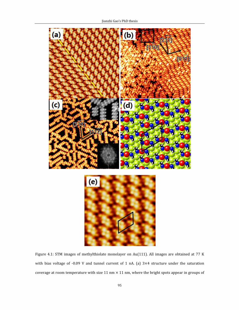
Jianzhi Gao’s PhD thesis
95
Figure 4.1: STM images of methylthiolate monolayer on Au(111). All images are obtained at 77 K
with bias voltage of -0.09 V and tunnel current of 1 nA. (a) 3 4 structure under the saturation
coverage at room temperature with size 11 nm 11 nm, where the bright spots appear in groups of
Jianzhi Gao’s PhD thesis
96
six. (b) STM image with size of 17 nm 17 nm. Thermal annealing the SAM at 330 K resulting in local
disorder of the monolayer and the appearance of the striped phase. (c) STM image with size of 20
nm 20 nm. Further annealing sample to 350 K, which causes complete disappearance of the 3 4
structure, where thiolate rows appear on the sample surface. The inset image at the upper right
corner shows detailed structure of the building block of the molecular rows. The lower right inset is a
Fourier transform of the STM image. (d) Structural model based on the Au-adatom-dithiolate scheme
proposed by Voznyy et al [111], where the red balls represent the Au adatoms, the blue balls
represent the S atoms and the black balls indicate the CH3 groups. The 3 4 unit cell is highlighted
and compared directly with the STM image in (e).
Figure 4.1 (b) shows a high-resolution STM image after the molecular monolayer
has been annealed at 330 K. According to this image, the right hand side retains the
3 4 structure, and the left part of the image appears as a disordered region. From
the upper left corner of the image, we can see clearly the newly formed striped
phase highlighted with a square box, where these striped rows are parallel to one of
the <11 > directions. Further annealing the sample at 350 K causes the
disappearance of the 3 4 structure and the formation of a new striped phase, which
is shown in figure 4.1 (c). The inset atomic resolution STM image at the upper right
corner shows the details of the stripe phases, and the lower right corner is a Fourier
transform of the STM image.
The striped phase in figure 4.1 (c) is very similar to that observed by Voznyy et al.
[111] According to their experiment, they deposited a small amount of DMDS
molecules on Au(111) at low temperature, then increased the substrate
temperature to 200 K to dissociate the molecules. They proposed the basic
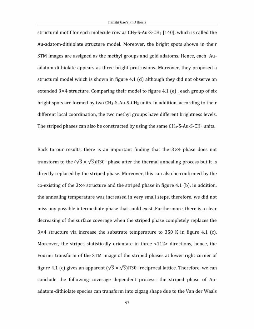
Jianzhi Gao’s PhD thesis
97
structural motif for each molecule row as CH3-S-Au-S-CH3 [140], which is called the
Au-adatom-dithiolate structure model. Moreover, the bright spots shown in their
STM images are assigned as the methyl groups and gold adatoms. Hence, each Au-
adatom-dithiolate appears as three bright protrusions. Moreover, they proposed a
structural model which is shown in figure 4.1 (d) although they did not observe an
extended 3 4 structure. Comparing their model to figure 4.1 (e) , each group of six
bright spots are formed by two CH3-S-Au-S-CH3 units. In addition, according to their
different local coordination, the two methyl groups have different brightness levels.
The striped phases can also be constructed by using the same CH3-S-Au-S-CH3 units.
Back to our results, there is an important finding that the 3 4 phase does not
transform to the R300 phase after the thermal annealing process but it is
directly replaced by the striped phase. Moreover, this can also be confirmed by the
co-existing of the 3 4 structure and the striped phase in figure 4.1 (b), in addition,
the annealing temperature was increased in very small steps, therefore, we did not
miss any possible intermediate phase that could exist. Furthermore, there is a clear
decreasing of the surface coverage when the striped phase completely replaces the
3 4 structure via increase the substrate temperature to 350 K in figure 4.1 (c).
Moreover, the stripes statistically orientate in three <112> directions, hence, the
Fourier transform of the STM image of the striped phases at lower right corner of
figure 4.1 (c) gives an apparent R300 reciprocal lattice. Therefore, we can
conclude the following coverage dependent process: the striped phase of Au-
adatom-dithiolate species can transform into zigzag shape due to the Van der Waals
Jianzhi Gao’s PhD thesis
98
interaction between the molecules and form 3 4 phase when its coverage reached
0.33 ML. For the lower coverage situation, the 3 4 phase changes into the striped
phase via an intermediate disordered phase. Hence, the transformation of the
different phases are totally controlled by the surface coverage of the Au-adatom-
dithiolate species. Moreover, the local bonding structure between the Au(111)
substrate and the Au-adatom-dithiolate is exactly the same for both striped phases
and the 3 4 phase. However, the lateral organization between adjacent dithiolate
species are different, in order to allow additional molecules packed into the 3 4
phase.
4.1.2 Absence of the 0 phase-ethylthiolate
monolayer.
To make a comparison to the methylthiolate monolayer, we also did the research
with the ethylthiolate monolayer on the Au(111) surface. The ethylthiolate
monolayer is formed by exposing Au(111) to 5 10-5 mbar of enthanethiol vapour at
room temperature for 2 hours. The STM image for the ethylthiolate monolayer is
shown in figure 4.2.
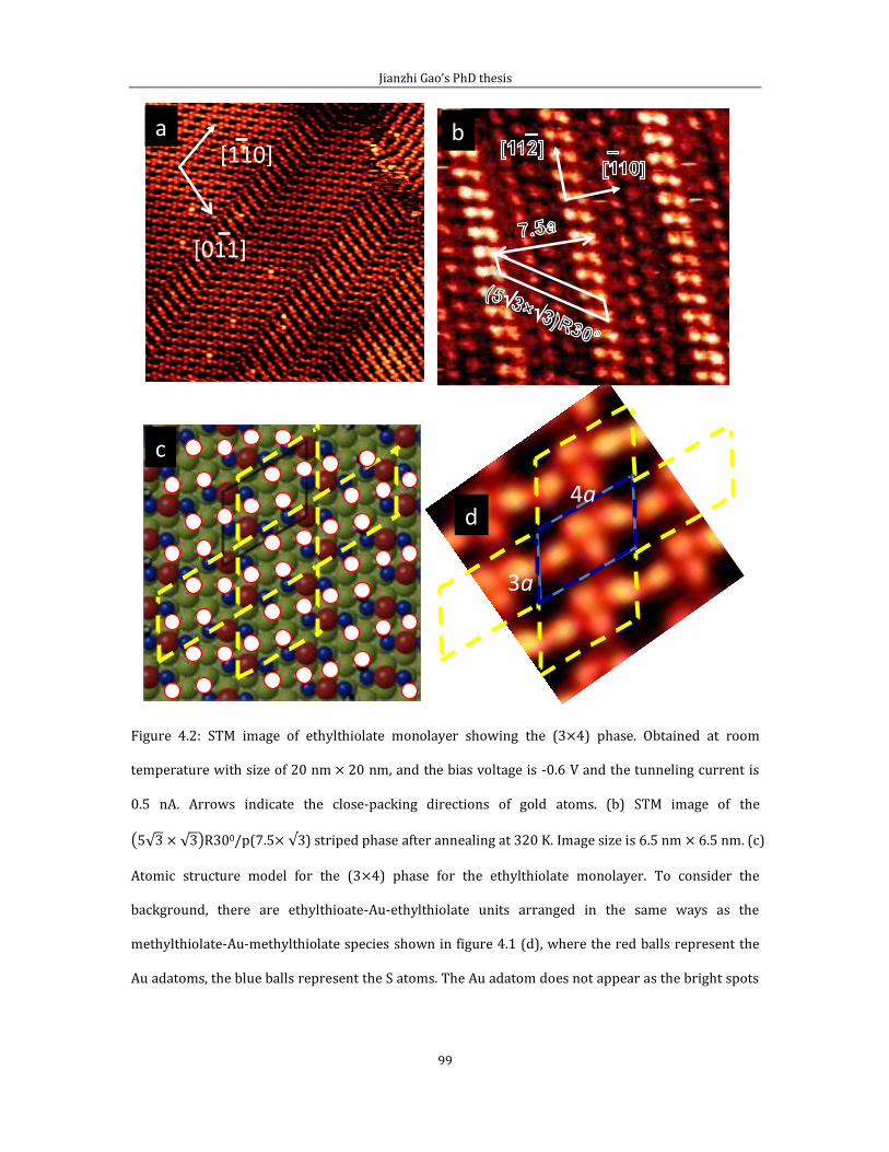
Jianzhi Gao’s PhD thesis
99
Figure 4.2: STM image of ethylthiolate monolayer showing the (3 4) phase. Obtained at room
temperature with size of 20 nm 20 nm, and the bias voltage is -0.6 V and the tunneling current is
0.5 nA. Arrows indicate the close-packing directions of gold atoms. (b) STM image of the
0/p(7.5 ) striped phase after annealing at 320 K. Image size is 6.5 nm 6.5 nm. (c)
Atomic structure model for the (3 4) phase for the ethylthiolate monolayer. To consider the
background, there are ethylthioate-Au-ethylthiolate units arranged in the same ways as the
methylthiolate-Au-methylthiolate species shown in figure 4.1 (d), where the red balls represent the
Au adatoms, the blue balls represent the S atoms. The Au adatom does not appear as the bright spots
a
d
b[110]
[011]
3a
4a
c
a b
d
Jianzhi Gao’s PhD thesis
100
and the bright white circles represent the methyl groups which is showing bright in the STM images.
(d) High resolution STM image, 2.4 nm 2.6 nm, consistent with the scheme depicted in (c).
The general atomic arrangement for the molecule monolayer in figure 4.2 (a) looks
very different when we compare it to that in figure 4.1 (a). However, the
ethylthiolate monolayer in figure 4.2 (a) has the same lattice structure as the
methylthiolate monolayer, both of them belong to the (3 4) phase and the domain
boundary structure in figure 4.2 (a) is also similar to the one shown in figure 4.1 (a).
The reason for the different appearance of the two molecular monolayers under the
STM images may attribute to the internal structure of the unit cell for both different
types of molecules. Ethylthiolate has a longer chain length than the methylthiolate.
Thus, the`CH3 group of the ethythiolate extends much more from the surface and
appears significantly taller than the gold adatom. Therefore, for ethylthiolate, the Au
adatom appears dark. In addition, there is some distortion for the STM image shown
in figure 4.2 (a), this is due to the drift of the VT-STM, which can stretch the
horizontal distance for the image at the room temperature. Moreover, we followed
the same experimental progress as the methylthiolate monolayer. We thermally
annealed the sample and we found the (3 4) structure is replaced by an ordered
striped phase, which is shown in figure 4.2 (b). Furthermore, we also observed the
co-existence of the striped phase with the (3 4) phase for the ethylthiolate
monolayer, and the R300 phase is still not found as the middle phase
during this phase transition. The striped phase shown in figure 4.2 (b) can be
obtained without the formation of the (3 4) structure if the gold sample is exposed
to ethanethiol at 320 K. According to the striped phase in figure 4.2 (b), the bright
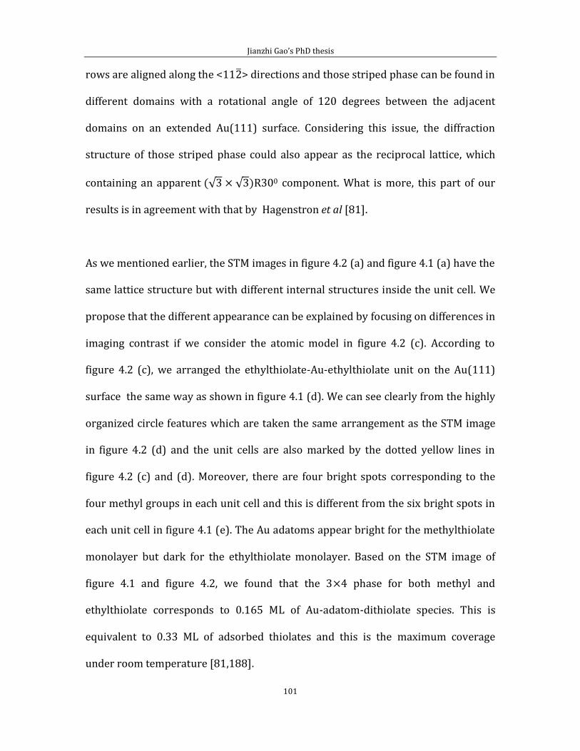
Jianzhi Gao’s PhD thesis
101
rows are aligned along the <11 > directions and those striped phase can be found in
different domains with a rotational angle of 120 degrees between the adjacent
domains on an extended Au(111) surface. Considering this issue, the diffraction
structure of those striped phase could also appear as the reciprocal lattice, which
containing an apparent R300 component. What is more, this part of our
results is in agreement with that by Hagenstron et al [81].
As we mentioned earlier, the STM images in figure 4.2 (a) and figure 4.1 (a) have the
same lattice structure but with different internal structures inside the unit cell. We
propose that the different appearance can be explained by focusing on differences in
imaging contrast if we consider the atomic model in figure 4.2 (c). According to
figure 4.2 (c), we arranged the ethylthiolate-Au-ethylthiolate unit on the Au(111)
surface the same way as shown in figure 4.1 (d). We can see clearly from the highly
organized circle features which are taken the same arrangement as the STM image
in figure 4.2 (d) and the unit cells are also marked by the dotted yellow lines in
figure 4.2 (c) and (d). Moreover, there are four bright spots corresponding to the
four methyl groups in each unit cell and this is different from the six bright spots in
each unit cell in figure 4.1 (e). The Au adatoms appear bright for the methylthiolate
monolayer but dark for the ethylthiolate monolayer. Based on the STM image of
figure 4.1 and figure 4.2, we found that the 3 4 phase for both methyl and
ethylthiolate corresponds to 0.165 ML of Au-adatom-dithiolate species. This is
equivalent to 0.33 ML of adsorbed thiolates and this is the maximum coverage
under room temperature [81,188].
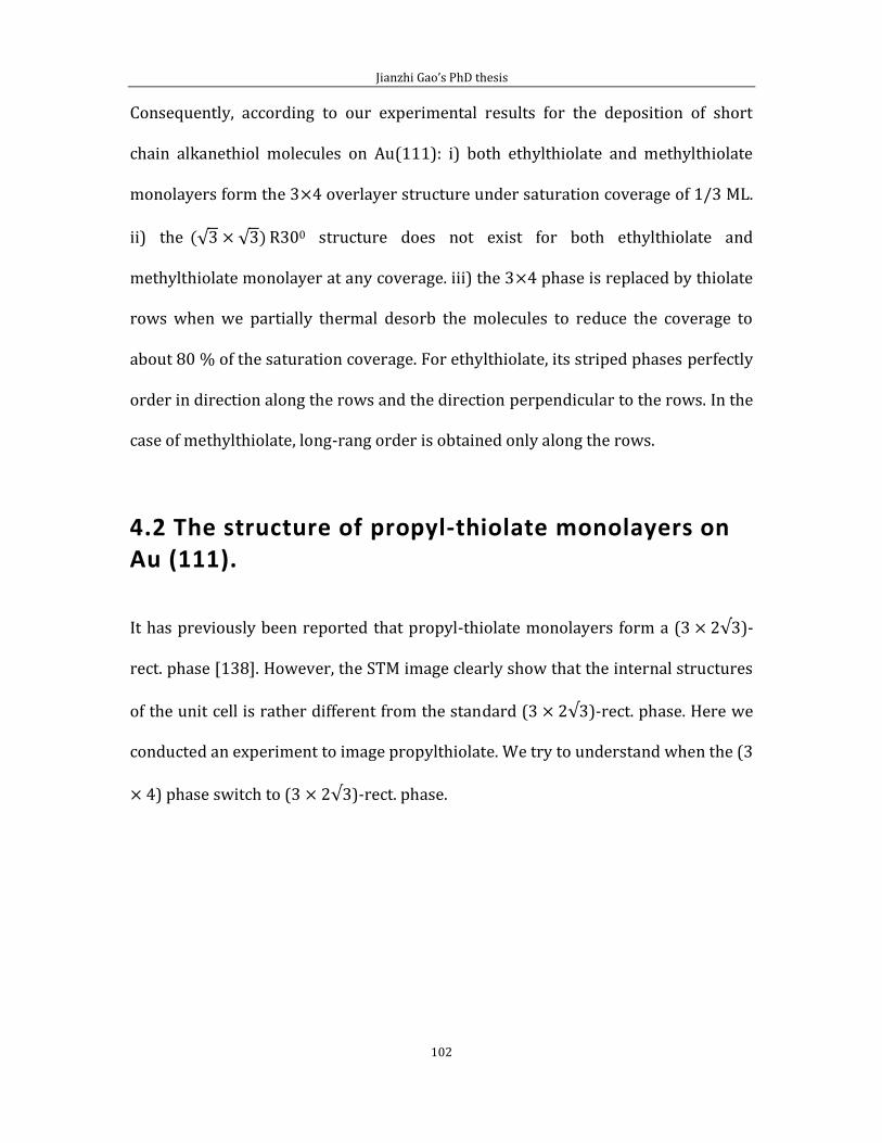
Jianzhi Gao’s PhD thesis
102
Consequently, according to our experimental results for the deposition of short
chain alkanethiol molecules on Au(111): i) both ethylthiolate and methylthiolate
monolayers form the 3 4 overlayer structure under saturation coverage of 1/3 ML.
ii) the R300 structure does not exist for both ethylthiolate and
methylthiolate monolayer at any coverage. iii) the 3 4 phase is replaced by thiolate
rows when we partially thermal desorb the molecules to reduce the coverage to
about 80 % of the saturation coverage. For ethylthiolate, its striped phases perfectly
order in direction along the rows and the direction perpendicular to the rows. In the
case of methylthiolate, long-rang order is obtained only along the rows.
4.2 The structure of propyl-thiolate monolayers on Au (111).
It has previously been reported that propyl-thiolate monolayers form a (3 2 )-
rect. phase [138]. However, the STM image clearly show that the internal structures
of the unit cell is rather different from the standard (3 2 )-rect. phase. Here we
conducted an experiment to image propylthiolate. We try to understand when the (3
4) phase switch to (3 2 )-rect. phase.
Jianzhi Gao’s PhD thesis
103
4.2.1 Short range ordered 3 4 phase-propylthiolate monolayer. A number of STM images, together with a structural model, are shown in figure 4.3.
Figure 4.3 (a) shows an STM image of a C3 monolayer in the 3 4 like phase. Unlike
C1 and C2 monolayers, the 3 4 phase of the C3 monolayer is broken into small
domains by defects. Therefore, this 3 4 like phase consists of a layer of densely
packed thiolate at a coverage slightly less than 1/3 ML. Figure 4.3 (b) is a higher
resolution STM image showing the 3 4 like phase and a 3 4 unit cell is illustrated.
STM images taken from the C3 monolayer with the VT-STM suffer from a noticeable
level of scanner drift causing distortion to the 3 4 lattice. The images shown here
have not been subject to any digital correction. The fundamental building block for
the 3 4 like phase is the AAD: CH3(CH2)2-S-Au-S-(CH2)2CH3. In figure 4.3 (c) short
bars are overlaid onto the image to highlight the AAD units. The blue bars represent
the AAD unit at the 3 4 region and the orange bars represent the AAD units in the
gaps. STM images show that every two AAD units appear to join to form a tetramer
in the 3 4 region [192]. Each tetramer shows two bright spots and two less bright
spots. These four spots are methyl groups at propyl tails, thus one of the methyl
groups is physically taller than the other. The sulfur atoms are invisible in the image
[189]. To compare with C2 monolayers, the same kind of AAD tetramer arrangement
exists, meanwhile, Au-adatom is not visible in the STM images under normal
imaging conditions for both C2 and C3 monolayers. This is probably because the
ethyl and propyl tails extend much more beyond the Au-adatom. Before analyzing
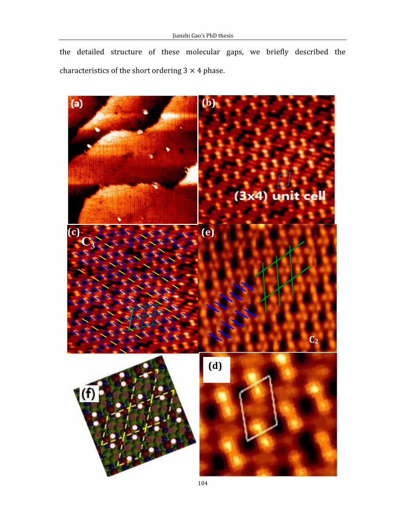
Jianzhi Gao’s PhD thesis
104
the detailed structure of these molecular gaps, we briefly described the
characteristics of the short ordering 3 4 phase.
(c) (e)
C2
(b) (a)
(d)
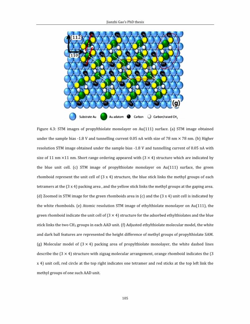
Jianzhi Gao’s PhD thesis
105
Figure 4.3: STM images of propylthiolate monolayer on Au(111) surface. (a) STM image obtained
under the sample bias -1.8 V and tunnelling current 0.05 nA with size of 78 nm 78 nm. (b) Higher
resolution STM image obtained under the sample bias -1.8 V and tunnelling current of 0.05 nA with
size of 11 nm 11 nm. Short range ordering appeared with (3 4) structure which are indicated by
the blue unit cell. (c) STM image of propylthiolate monolayer on Au(111) surface, the green
rhomboid represent the unit cell of (3 x 4) structure, the blue stick links the methyl groups of each
tetramers at the (3 x 4) packing area , and the yellow stick links the methyl groups at the gaping area.
(d) Zoomed in STM image for the green rhomboids area in (c) and the (3 x 4) unit cell is indicated by
the white rhomboids. (e) Atomic resolution STM image of ethylthiolate monolayer on Au(111), the
green rhomboid indicate the unit cell of (3 4) structure for the adsorbed ethylthiolates and the blue
stick links the two CH3 groups in each AAD unit. (f) Adjusted ethylthiolate molecular model, the white
and dark ball features are represented the height difference of methyl groups of propylthiolate SAM.
(g) Molecular model of (3 4) packing area of propylthiolate monolayer, the white dashed lines
describe the (3 4) structure with zigzag molecular arrangement, orange rhomboid indicates the (3
x 4) unit cell, red circle at the top right indicates one tetramer and red sticks at the top left link the
methyl groups of one such AAD unit.
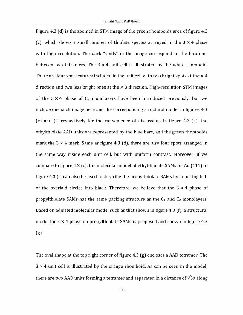
Jianzhi Gao’s PhD thesis
106
Figure 4.3 (d) is the zoomed in STM image of the green rhomboids area of figure 4.3
(c), which shows a small number of thiolate species arranged in the 3 4 phase
with high resolution. The dark “voids” in the image correspond to the locations
between two tetramers. The 3 4 unit cell is illustrated by the white rhomboid.
There are four spot features included in the unit cell with two bright spots at the 4
direction and two less bright ones at the 3 direction. High-resolution STM images
of the 3 4 phase of C2 monolayers have been introduced previously, but we
include one such image here and the corresponding structural model in figures 4.3
(e) and (f) respectively for the convenience of discussion. In figure 4.3 (e), the
ethylthiolate AAD units are represented by the blue bars, and the green rhomboids
mark the 3 4 mesh. Same as figure 4.3 (d), there are also four spots arranged in
the same way inside each unit cell, but with uniform contrast. Moreover, if we
compare to figure 4.2 (c), the molecular model of ethylthiolate SAMs on Au (111) in
figure 4.3 (f) can also be used to describe the propylthiolate SAMs by adjusting half
of the overlaid circles into black. Therefore, we believe that the 3 4 phase of
propylthiolate SAMs has the same packing structure as the C1 and C2 monolayers.
Based on adjusted molecular model such as that shown in figure 4.3 (f), a structural
model for 3 4 phase on propylthiolate SAMs is proposed and shown in figure 4.3
(g).
The oval shape at the top right corner of figure 4.3 (g) encloses a AAD tetramer. The
3 4 unit cell is illustrated by the orange rhomboid. As can be seen in the model,
there are two AAD units forming a tetramer and separated in a distance of a along
Jianzhi Gao’s PhD thesis
107
the [11 ] direcion, each tetramer is separated by 4a from its neighbor along the
[1 0] direction. The tetramers located at the up and down positions are shifted with
a 1a distance along the 3 direction, hence form the 3 4 structure consisting of
zig-zag rows of AAD units. The white dashed lines indicate the zig-zag molecular
rows in the model. Based on the model in figure 4.3 (g) for each AAD, the two propyl
chains are in different environment. The chain in grey colour is confined by S and
the Au adatom. So it cannot tilt too much towards the surface. The other chain, in
black colour, can extend more freely towards the surface. Hence the “grey” chain is
expected to be taller.
With the fundamental features of the 3 4 phase presented above, we now focus on
the structure of the gap area. Figure 4.4 (a) shows an STM image of a C3 monolayer
with narrow 3 4 domains. These narrow domains are separated by gaps. The gaps
are filled by AAD units as well. It can be seen in figure 4.4 (a), in some area, for every
two bright rows there is a gap. In other areas for every row of bright spots, there is a
gap. The above two arrangements give two ordered structures. We call them type 1
and type 2 respectively. The boundaries of type 1 structure are highlighted by green
lines and the boundaries of type 2 structure are highlighted by the white lines in
figure 4.4 (a). From the previous discussion in figure 4.3 (c), we realize from the
overlaid blue bars that the bright spots comes from the raised methyl groups.
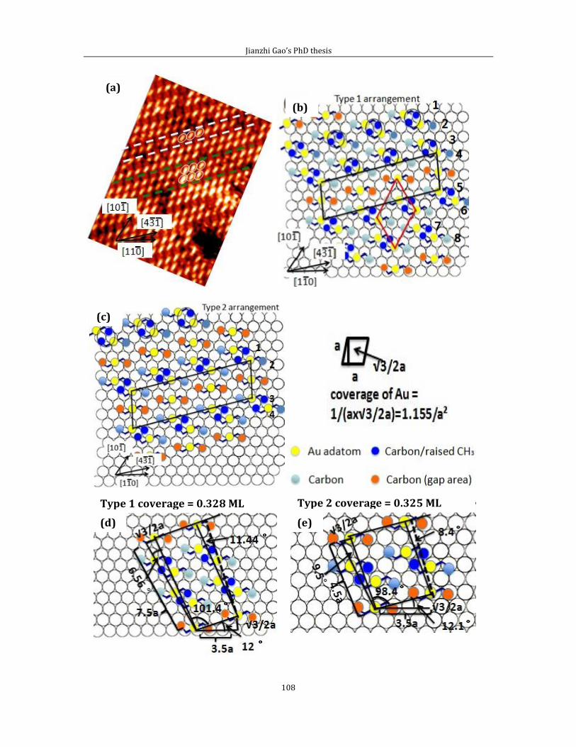
Jianzhi Gao’s PhD thesis
108
(a)
(b)
(c)
(d) (e)
Type 1 coverage = 0.328 ML Type 2 coverage = 0.325 ML
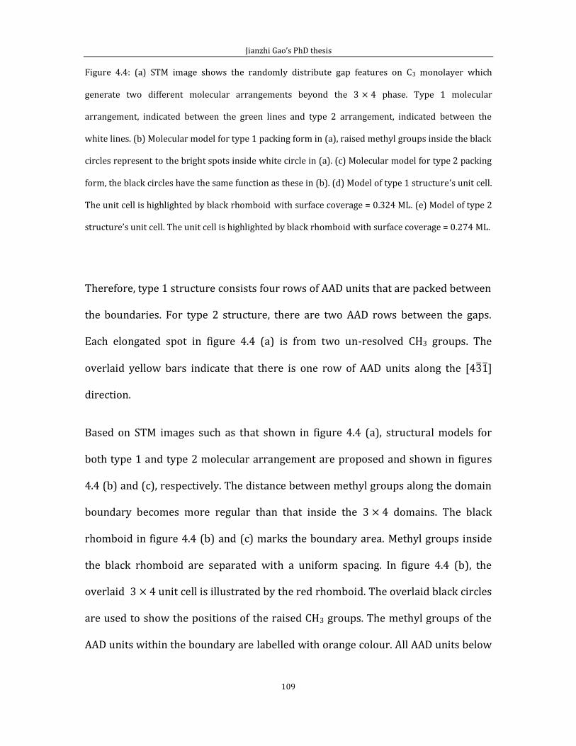
Jianzhi Gao’s PhD thesis
109
Figure 4.4: (a) STM image shows the randomly distribute gap features on C3 monolayer which
generate two different molecular arrangements beyond the 3 4 phase. Type 1 molecular
arrangement, indicated between the green lines and type 2 arrangement, indicated between the
white lines. (b) Molecular model for type 1 packing form in (a), raised methyl groups inside the black
circles represent to the bright spots inside white circle in (a). (c) Molecular model for type 2 packing
form, the black circles have the same function as these in (b). (d) Model of type 1 structure’s unit cell.
The unit cell is highlighted by black rhomboid with surface coverage = 0.324 ML. (e) Model of type 2
structure’s unit cell. The unit cell is highlighted by black rhomboid with surface coverage = 0.274 ML.
Therefore, type 1 structure consists four rows of AAD units that are packed between
the boundaries. For type 2 structure, there are two AAD rows between the gaps.
Each elongated spot in figure 4.4 (a) is from two un-resolved CH3 groups. The
overlaid yellow bars indicate that there is one row of AAD units along the [4 ]
direction.
Based on STM images such as that shown in figure 4.4 (a), structural models for
both type 1 and type 2 molecular arrangement are proposed and shown in figures
4.4 (b) and (c), respectively. The distance between methyl groups along the domain
boundary becomes more regular than that inside the 3 4 domains. The black
rhomboid in figure 4.4 (b) and (c) marks the boundary area. Methyl groups inside
the black rhomboid are separated with a uniform spacing. In figure 4.4 (b), the
overlaid 3 4 unit cell is illustrated by the red rhomboid. The overlaid black circles
are used to show the positions of the raised CH3 groups. The methyl groups of the
AAD units within the boundary are labelled with orange colour. All AAD units below
Jianzhi Gao’s PhD thesis
110
the boundary are shifted, relative to those above the boundary, by a distance “ a”
in the 4 direction, where “a” is the nearest neighbour distance of surface gold
atoms. Figure 4.4 (c) shows the same translational shift between the 3 4 domain
and the boundaries. To consider both models in figures 4.4 (b) and (c), the
connection area of both sides of the 3 4 domain has a rhomboid shape, which is
long in the [4 ] direction, but narrow in the [11 ] direction. The width, as seen in
both models, spans only two tetramer distances which formed a shortest periodic
striped phased for propylthiolates. For C3 monolayers with saturation coverage,
only the short range ordered 3 4 phases are observed in our experiment,
suggesting that the extended 3 4 phase is less stable. There could be several
reasons why an extended 3 4 domain is less stable for C3 monolayers. The most
probable one is stress relieve within the layer. It can be seen from figure 4.3 (g). the
distance between the propyl chains is not uniform, and repulsive interaction
between closely-spaced chains is possible. This repulsive interaction would scale
with the alkane chain length. Therefore, too much repulsion is involved in the 3 4
phase for C3. By forming structures of type 1 and 2, some stress is relieved.
In terms of thiolate coverage, the boundaries appeared in the models of type 1 and
type 2 structures, causes a decrease in coverage of the monolayer. The unit cell
structures of type 1 and 2 structures are indicated as black rhomboid in figures 4.4
(d) and (e) respectively, the additional figure at right side of (c) shows the
calculation of surface coverage of gold inside the unit area, which is 1.155/a2. To
Jianzhi Gao’s PhD thesis
111
calculate the surface coverage of both type of structures, we created the right
triangle structure on both the long and the narrow sides of the rhomboids, hence to
calculate the side distance and area of each unit cell, then count the number of
methyl groups inside the unit cell area. When we calculate the surface coverage by
comparing this with surface coverage of gold inside the unit area (1.155/a2). There
are 10 methyl groups inside the unit cell of type 1 structure and the unit cell area is
26.55 a2, which gives the number of CH3 per unit area 0.3766/a2. Therefore, the
surface coverage of type 1 structure is 0.328 ML. For type 2 structure, there are 6
methyl groups inside the 16 a2 unit cell. The surface coverage of type 2 structure is
thus 0.325 ML.
From the previous discussion in figure 4.3 (g), we are aware that the methyl groups
of each AAD unit have different heights. Half of the methyl groups of AAD units
appear higher. As a result, this kind of methyl groups are brighter in the STM images.
The rest of the methyl groups within the 3 4 domain, as well as those within the
boundaries appear less bright. However, these dark methyls could be imaged with
better contrast under the appropriate scanning condition. Figure 4.5 (a) shows an
STM image with topographical view of C3 monolayer under high and low bias
voltages. The upper 1/3 of the image was obtained with -1.5 V, the lower 2/3 of the
image was obtained with -0.15 V. Line AB is used to guide the eyes. Under -1.5 V, the
image has the same characteristics as that in figure 4.4 (a). With a lower voltage of -
0.15 V, the tip moves closer to the surface.
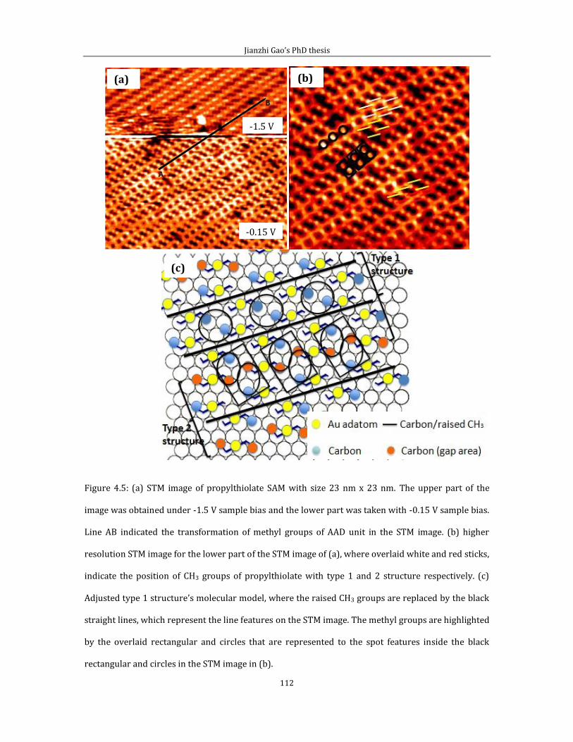
Jianzhi Gao’s PhD thesis
112
Figure 4.5: (a) STM image of propylthiolate SAM with size 23 nm x 23 nm. The upper part of the
image was obtained under -1.5 V sample bias and the lower part was taken with -0.15 V sample bias.
Line AB indicated the transformation of methyl groups of AAD unit in the STM image. (b) higher
resolution STM image for the lower part of the STM image of (a), where overlaid white and red sticks,
indicate the position of CH3 groups of propylthiolate with type 1 and 2 structure respectively. (c)
Adjusted type 1 structure’s molecular model, where the raised CH3 groups are replaced by the black
straight lines, which represent the line features on the STM image. The methyl groups are highlighted
by the overlaid rectangular and circles that are represented to the spot features inside the black
rectangular and circles in the STM image in (b).
-1.5 V
-0.15 V
(a) (b)
(c)
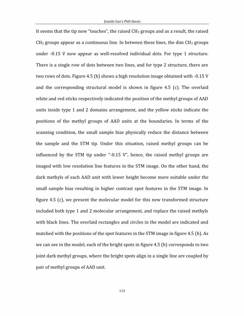
Jianzhi Gao’s PhD thesis
113
It seems that the tip now “touches”, the raised CH3 groups and as a result, the raised
CH3 groups appear as a continuous line. In between these lines, the dim CH3 groups
under -0.15 V now appear as well-resolved individual dots. For type 1 structure.
There is a single row of dots between two lines, and for type 2 structure, there are
two rows of dots. Figure 4.5 (b) shows a high resolution image obtained with -0.15 V
and the corresponding structural model is shown in figure 4.5 (c). The overlaid
white and red sticks respectively indicated the position of the methyl groups of AAD
units inside type 1 and 2 domains arrangement, and the yellow sticks indicate the
positions of the methyl groups of AAD units at the boundaries. In terms of the
scanning condition, the small sample bias physically reduce the distance between
the sample and the STM tip. Under this situation, raised methyl groups can be
influenced by the STM tip under “-0.15 V”, hence, the raised methyl groups are
imaged with low resolution line features in the STM image. On the other hand, the
dark methyls of each AAD unit with lower height become more suitable under the
small sample bias resulting in higher contrast spot features in the STM image. In
figure 4.5 (c), we present the molecular model for this new transformed structure
included both type 1 and 2 molecular arrangement, and replace the raised methyls
with black lines. The overlaid rectangles and circles in the model are indicated and
matched with the positions of the spot features in the STM image in figure 4.5 (b). As
we can see in the model, each of the bright spots in figure 4.5 (b) corresponds to two
joint dark methyl groups, where the bright spots align in a single line are coupled by
pair of methyl groups of AAD unit.
Jianzhi Gao’s PhD thesis
114
4.2.2 Adsorption of methyl-propyl disulfide on Au(111)
In this section, I will discuss experimental results obtained from a self-assembled
monolayer prepared by dosing Au(111) with methyl-propyl-disulfide (MPDS), CH3-
S-S-(CH2)2CH3. When a MPDS molecule lands on the surface, one of the following
processes would occur: 1) Direct combination of MPDS with a Au atom to form CH3-
S-Au-S-(CH2)2CH3 which will be referred to as C1S-Au-SC3. If this is the only process,
then the molecular layer would consist of only C1S-Au-SC3. 2) MPDS molecule
dissociates giving rise to: CH3S and CH3(CH2)2S. Further reaction to Au atoms forms
CH3S-Au and CH3(CH2)2S-Au. In this case, at any monoment, there are seven
different species on the surface: CH3S, CH3(CH2)2S, CH3S-Au, CH3(CH2)2S-Au, CH3-S-
CH3, CH3(CH2)2S-Au-S-CH3, and CH3(CH2)2-S-Au-S-(CH2)2CH3. We will refer the three
AAD as C1S-Au-SC3, C1S-Au-SC1, C3S-Au-SC3, respectively.
Up to now, there is no clear view as to which of the above two process occurs. Figure
4.6 (a) shows an STM image which gives the overall view of the molecular layer
formed after exposing the sample at room temperature to 10-5 mbar of MPDS
vapour for one hour. This image shows no long-range order. The sample was then
thermally annealed to 320 K for 30 minutes. After cooling down to RT, the sample
was imaged again.
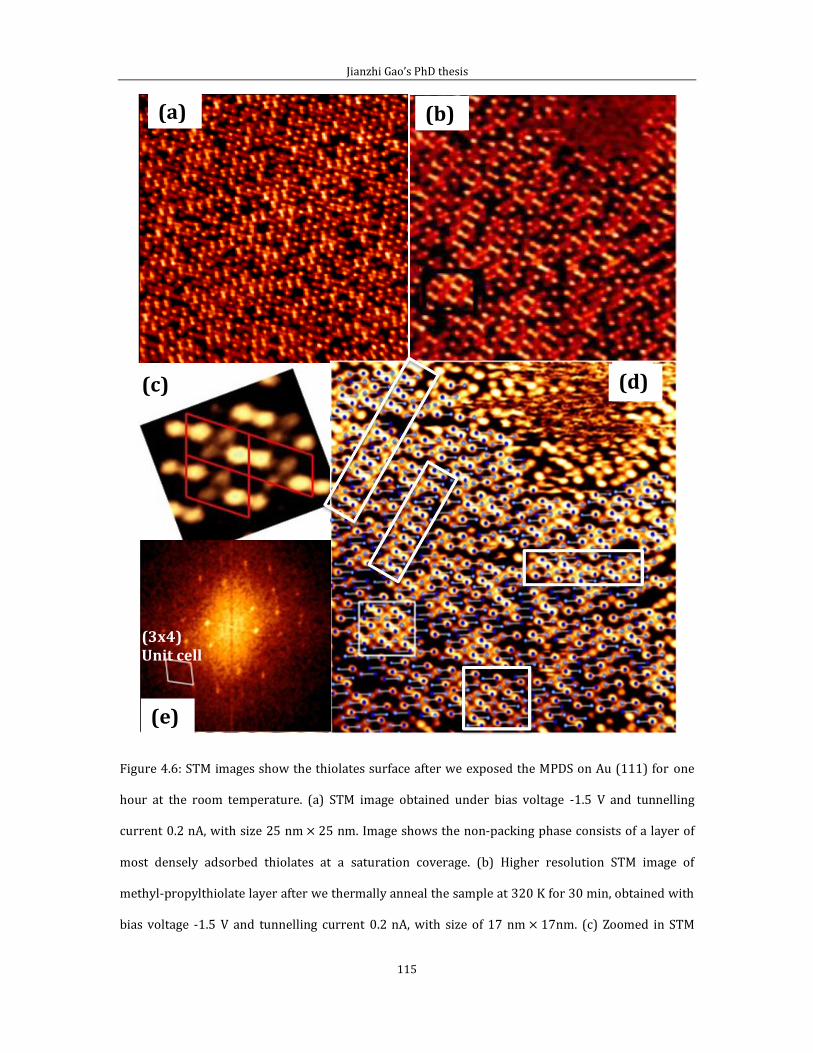
Jianzhi Gao’s PhD thesis
115
Figure 4.6: STM images show the thiolates surface after we exposed the MPDS on Au (111) for one
hour at the room temperature. (a) STM image obtained under bias voltage -1.5 V and tunnelling
current 0.2 nA, with size 25 nm 25 nm. Image shows the non-packing phase consists of a layer of
most densely adsorbed thiolates at a saturation coverage. (b) Higher resolution STM image of
methyl-propylthiolate layer after we thermally anneal the sample at 320 K for 30 min, obtained with
bias voltage -1.5 V and tunnelling current 0.2 nA, with size of 17 nm 17nm. (c) Zoomed in STM
(a)
(e)
(3x4) Unit cell
(c) (d)
(a) (b)
Jianzhi Gao’s PhD thesis
116
images of black rectangles in (b), unit cells with the (3 4) phase of propylthiolates are illustrated by
the red rhomboids. (d) STM image with overlaid square and rectangles which are indicated the
position of packed domain on the monolayer and each AAD units is represented by two different
colored balls linked by a stick. The dark color balls repersent the bright spots in the STM image and
the light colored balls repersent the less bright spots or some dark area in the STM image. (e) FFT of
(d). The white rhomboid indicated the (3 4) unit cell.
Figure 4.6 (b) shows the corresponding STM image. The packing order is still poor
in comparison with MT and ET monolayers. However, some degree of ordering has
appeared after annealing. Localised 3 4 domains are observed. The domains are
rather small in size. Figure 4.6 (c) shows the 3 4 structure inside the black
rectangle in (b). The image in figure 4.6 (c) is from an area where the 3 4 is
formed by C3S-Au-SC3. The bright and dim contrast has been explained in the
previous section. The structure of the unit cell is the same as that found for MT and
ET monolayers.
The existence of the 3 4 phase shows that we have AAD in the molecular layer. But
there can be up to three types of AAD according to process No.2 described above.
The consequence of AAD formation is that all the spots in the image are paired.
Using the localised 3 4 domains as guidance, we performed a pairing process for
the image shown in figure 4.6 (b). Figure 4.6 (d) shows the result of the pairing
operation. A direct result of the pairing is that the molecular layer is denser than it
appears. This is because there are “hidden” spots which are only found using the
pairing procedure. According to figure 4.6 (d), there are three levels of brightness
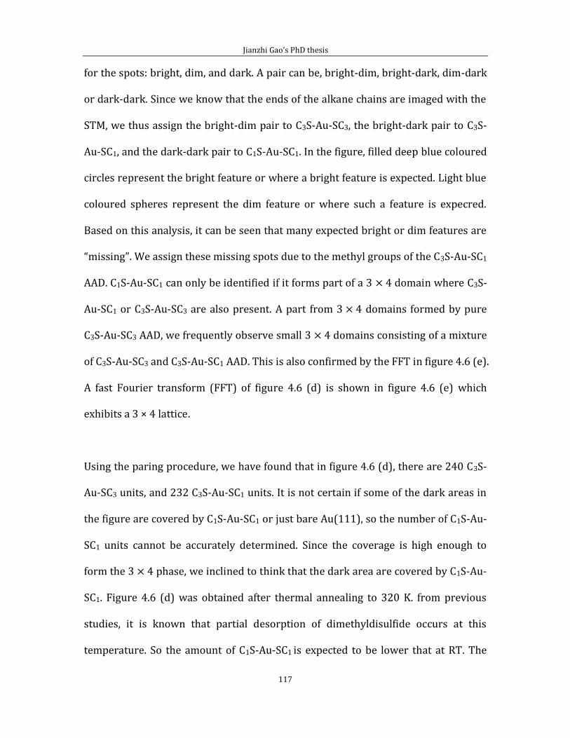
Jianzhi Gao’s PhD thesis
117
for the spots: bright, dim, and dark. A pair can be, bright-dim, bright-dark, dim-dark
or dark-dark. Since we know that the ends of the alkane chains are imaged with the
STM, we thus assign the bright-dim pair to C3S-Au-SC3, the bright-dark pair to C3S-
Au-SC1, and the dark-dark pair to C1S-Au-SC1. In the figure, filled deep blue coloured
circles represent the bright feature or where a bright feature is expected. Light blue
coloured spheres represent the dim feature or where such a feature is expecred.
Based on this analysis, it can be seen that many expected bright or dim features are
“missing”. We assign these missing spots due to the methyl groups of the C3S-Au-SC1
AAD. C1S-Au-SC1 can only be identified if it forms part of a 3 4 domain where C3S-
Au-SC1 or C3S-Au-SC3 are also present. A part from 3 4 domains formed by pure
C3S-Au-SC3 AAD, we frequently observe small 3 4 domains consisting of a mixture
of C3S-Au-SC3 and C3S-Au-SC1 AAD. This is also confirmed by the FFT in figure 4.6 (e).
A fast Fourier transform (FFT) of figure 4.6 (d) is shown in figure 4.6 (e) which
exhibits a 3 × 4 lattice.
Using the paring procedure, we have found that in figure 4.6 (d), there are 240 C3S-
Au-SC3 units, and 232 C3S-Au-SC1 units. It is not certain if some of the dark areas in
the figure are covered by C1S-Au-SC1 or just bare Au(111), so the number of C1S-Au-
SC1 units cannot be accurately determined. Since the coverage is high enough to
form the 3 4 phase, we inclined to think that the dark area are covered by C1S-Au-
SC1. Figure 4.6 (d) was obtained after thermal annealing to 320 K. from previous
studies, it is known that partial desorption of dimethyldisulfide occurs at this
temperature. So the amount of C1S-Au-SC1 is expected to be lower that at RT. The
Jianzhi Gao’s PhD thesis
118
significance of the result shown here is that dissociation of C1S-SC3 occurs followed
by the formation of C1S-Au- and C3S-Au-, and then the Au-adatom-dithiolate.
Statistically C1S-Au-SC1: C3S-Au-SC3: C3S-Au-SC1 should be 1:1:2.
We now discuss how the 3 4 phase is related to other phases reported. In figure
4.7, we have included STM images from MT, ET, PT and MPT (methyl-propylthiolate)
monolayers (a to d). They all have the same 3 4 structure. The overlaid sticks are
used to highlight the AAD units in each case. An important feature of the 3 4 phase
is that the alkane chains are not regularly spaced. The Van der Waals interaction
between the chains favours a more regular spacing. Therefore, the formation of the
3 4 phase involves some stress within the molecular layer. The formation of type
1 and 2 structures observed for PT monolayers is a result of stress relieve. The
stress prevents the formation of a long-range-ordered 3 4 phase for PT. The
molecular model for PT monolayers is illustrated in figure 4.7 (f).
For alkanethiols with even longer chains, the Van der Waals interaction scales with
the chain length, so there must be a point where stress is so high that the 3 4
phase becomes unstable. This happens for butylthiolate monolayers which does not
form the 3 4 phase. Instead, it forms the well known (3 2√3)-rect. phase.
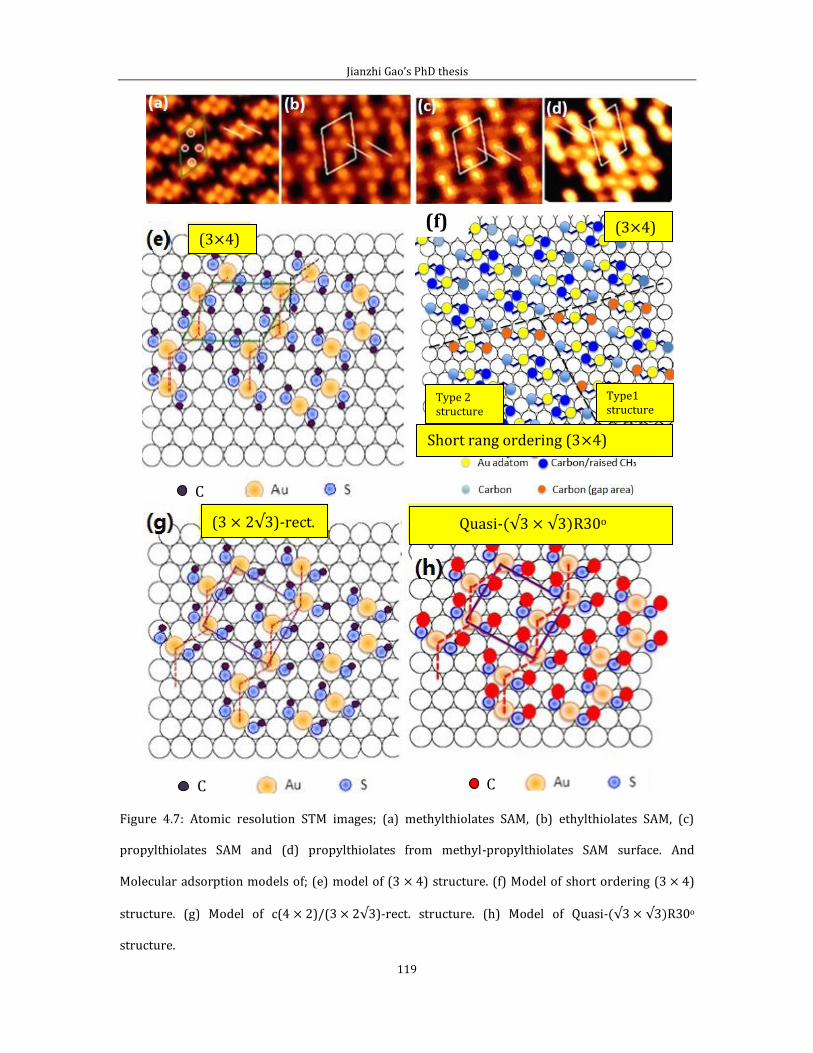
Jianzhi Gao’s PhD thesis
119
Figure 4.7: Atomic resolution STM images; (a) methylthiolates SAM, (b) ethylthiolates SAM, (c)
propylthiolates SAM and (d) propylthiolates from methyl-propylthiolates SAM surface. And
Molecular adsorption models of; (e) model of (3 4) structure. (f) Model of short ordering (3 4)
structure. (g) Model of c(4 2)/(3 )-rect. structure. (h) Model of Quasi- 3 R30o
structure.
C
C
C
(3 4) (3 4)
Type 2 structure
Type1 structure
Short rang ordering (3 4)
(3 )-rect. Quasi- 3 R30o
(f)
Jianzhi Gao’s PhD thesis
120
By comparing the ball model in figure 4.7 (e) for the 3 4 phase and that in figure
4.7 (g) for the (3 2√3)-rect. phase, it can be seen that these two phases are
related. They both are formed by zig-zag rows of AAD as indicate by the dashed lines.
The only difference is the relative position between two neighbouring zig-zag rows.
For the 3 4 phase, all rows follow the same zig-zag sequence. For the (3 2√3)-
rect. phase, one row is zig-zag, the next row is zag-zig.
The other difference is that AAD are all trans in 3 4 while this changes to all cis in
the (3 2√3)-rect. phase. There is no change in surface coverage. It can be seen
that by changing from the 3 4 to (3 2√3)-rect., the alkane chains become more
regularly spaced. For very long alkane chains, the spacing between alkane chains is
very uniform apart form the interfacial region. Thus, looking from above, the ends of
the alkane chains would appear to have a (√3 × √3)R30o structure as shown in figure
4.7 (h).
4.2.3 Propylthiolate striped phases
In the previous section, we have shown that after thermal annealing to 320 K, 3 4
domains consisting mixed C3S-Au-SC3 and C3S-Au-SC1 AAD are formed on the
surface. Thermal annealing has a rather complex effect on the monolayer.
Accompanied by partial desorption of C1S-SC1, there is also surface diffusion and
phase separation leading to many different structures on the surface. To make
things easier, we have raised the annealing temperature to 400 K. After annealing at
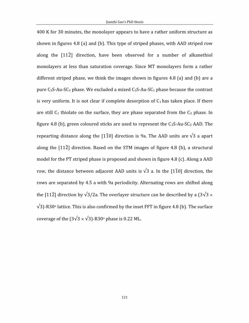
Jianzhi Gao’s PhD thesis
121
400 K for 30 minutes, the monolayer appears to have a rather uniform structure as
shown in figures 4.8 (a) and (b). This type of striped phases, with AAD striped row
along the [11 ] direction, have been observed for a number of alkanethiol
monolayers at less than saturation coverage. Since MT monolayers form a rather
different striped phase, we think the images shown in figures 4.8 (a) and (b) are a
pure C3S-Au-SC3 phase. We excluded a mixed C3S-Au-SC1 phase because the contrast
is very uniform. It is not clear if complete desorption of C1 has taken place. If there
are still C1 thiolate on the surface, they are phase separated from the C3 phase. In
figure 4.8 (b), green coloured sticks are used to represent the C3S-Au-SC3 AAD. The
repearting distance along the [1 0] direction is 9a. The AAD units are 3 a apart
along the [11 ] direction. Based on the STM images of figure 4.8 (b), a structural
model for the PT striped phase is proposed and shown in figure 4.8 (c). Along a AAD
row, the distance between adjacent AAD units is 3 a. In the [1 0] direction, the
rows are separated by 4.5 a with 9a periodicity. Alternating rows are shifted along
the [11 ] direction by 3/2a. The overlayer structure can be described by a (3 3
3)-R30o lattice. This is also confirmed by the inset FFT in figure 4.8 (b). The surface
coverage of the (3 3 3)-R30o phase is 0.22 ML.
Jianzhi Gao’s PhD thesis
122
Figure 4.8: STM images show the propylthiolate striped phases after the sample is annealed at 400 K
for 30 min. (a) STM images for the propylthiolate striped phase appear on different steps, obtained
with sample bias -2 V and tunnelling current 0.03 nA with size of 76 nm 76 nm. (b) Molecular
resoulution STM image of the propylthiolate striped phase after thermal annealing process which we
assign as ( )R300 with surface coverage of 0.22 ML. Obtained with sample bias -1 V and
tunnelling current 0.05 nA with size 6 nm 6 nm. Inset is an FFT of the image showing the high
quality of ordering and the (3√3 × √3)-R30o unit cell. (c) Molecular model of ( )R300 phase
base on the STM image in (b).
0.22 ML
(a) (b)
(c)
Jianzhi Gao’s PhD thesis
123
We started with a monolayer coverage of 1/3 ML, if all C1 thiols desorb and no
desorption of C3, then there would be 1/6 ML of C3 species left. Since the (3 3 3)-
R30o phase has a coverage much higher than 1/6 ML, there could be some residual
C1 left on the surface. Similar to ET monolayers, there are more than one type of
striped phases for the PT monolayer. When the surface coverage is changed, the
striped rows adjust their distance to cover as much the surface as possible. Fig. 4.9
(a) shows another example of the striped phase.
This type of striped phases, with AAD striped rows also along the [11 ] direction.
We think the images shown in figure 4.9 (a) is a pure lie-down C3S-Au-SC3 phase. In
figure 4.9 (a), the repearting distance of AAD units along the [1 0] direction is 11a.
The AAD units are 3 a apart along the [11 ] direction. Based on the STM images of
Fig. 4.9 (a), a structural model for this PT striped phase is proposed and shown in
Fig. 4.9 (b). Neighbouring stripes are separated by a distance with a period equal to
11a and the coverage equals to 0.18 ML. Alternating rows are shifted along the [11 ]
direction by 3a. All the striped phases have a common feature that they have rows
paralle to the [11 ] direction. The distance between neibouring rows are depends
on overall surface coverage.
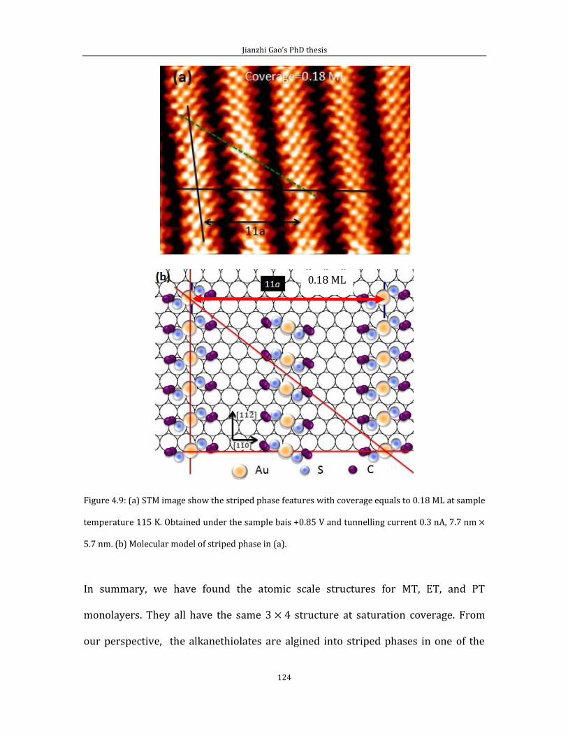
Jianzhi Gao’s PhD thesis
124
Figure 4.9: (a) STM image show the striped phase features with coverage equals to 0.18 ML at sample
temperature 115 K. Obtained under the sample bais +0.85 V and tunnelling current 0.3 nA, 7.7 nm
5.7 nm. (b) Molecular model of striped phase in (a).
In summary, we have found the atomic scale structures for MT, ET, and PT
monolayers. They all have the same 3 4 structure at saturation coverage. From
our perspective, the alkanethiolates are algined into striped phases in one of the
0.18 ML
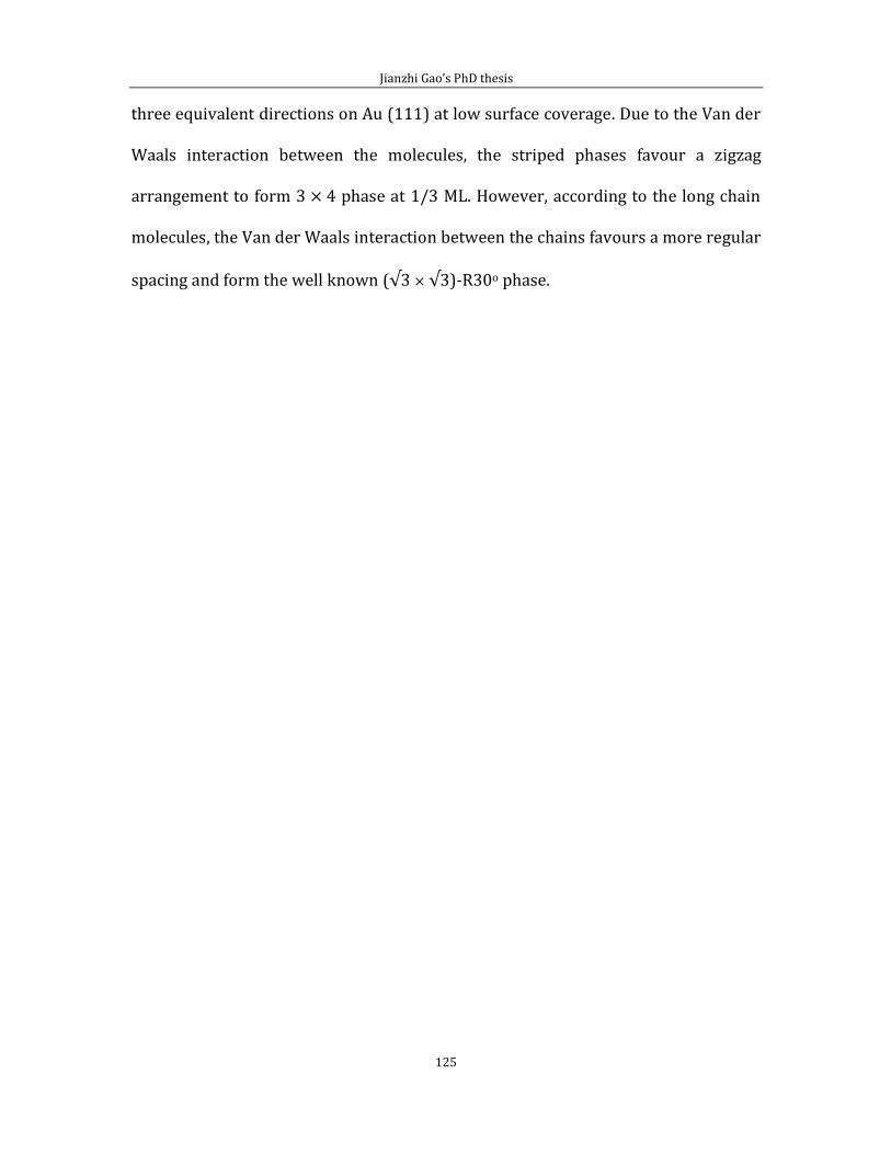
Jianzhi Gao’s PhD thesis
125
three equivalent directions on Au (111) at low surface coverage. Due to the Van der
Waals interaction between the molecules, the striped phases favour a zigzag
arrangement to form 3 4 phase at 1/3 ML. However, according to the long chain
molecules, the Van der Waals interaction between the chains favours a more regular
spacing and form the well known ( 3 3)-R30o phase.
Jianzhi Gao’s PhD thesis
126
Chapter 5 Low energy sputtering with argon and nitrogen on HOPG (0001)
In this chapter, I will present results for nitrogen deposition onto HOPG. We used a
standard cold cathode sputtering ion gun to generate charged nitrogen species. The
ions have kinetic energy of around 250 eV, which is sufficient to knock out carbon
atoms. I started the investigation using Ar+ ions. In the next section, I will show
results from Ar+ bombarded HOPG. The ion dose is controlled to near a minimum to
allow good quality STM images to be obtained.
5.1 Low energy Argon ion bombardment of HOPG (0001)
Argon implantation on the graphite surface has been done by many groups as
discussed in chapter 2. The purpose of this experiment is to make a reference for
nitrogen implantation.
Figure 5.1 (a) shows the morphology of the graphite surface after low energy Ar+ ion
bombardment. We can see some bright features which are point defects generated
during the argon ion bombardment process. There are at least two reasons why Ar+
bombardment produces these bright spots. One is point defect caused by removal of
a carbon atom from the top layer [174]. This gives rise to the creation of dangling
bonds around the vacancy.
Jianzhi Gao’s PhD thesis
127
Figure 5.1: HOPG (0001) surface after Ar ion bombardment with ion beam energy of 250 eV, current
density 3nA/c . (a) STM image, 150 nm 150 nm, obtained with bias voltage of +0.2 V and
tunnelling current of 0.6 nA. (b) STM image, 22 nm 22 nm, showing with bias voltage +0.2 V and
tunnelling current 0.6 nA.
Another is interstitial defects, which is caused by the argon ions or carbon atoms
trapped between two layers of carbon atoms [175], thus the physical height of the
surface of graphite will increase and cause the bright points in the STM images.
Because STM images are influenced by both the geometric and electronic structure,
it is never easy to make an accurate judgement of a particular feature based on the
appearance of the image. This is particularly true for isolated, non periodic features
such as those shown in figure 5.1. Amara et al [183] analysed the electronic
structure of several types of point defects on graphite and their connection with
STM images. The difference between vacancy defect and interstitial defect has been
addressed by Hahn and Kang [184]. They find that there is more than an order of
magnitude increase in the local density of states near the Fermi level around a
Jianzhi Gao’s PhD thesis
128
vacancy in comparison with perfect graphite surface. Increase in local density of
states also occurs at interstitial defects, but the change is much smaller. Base on this,
they suggested that the most bright features are due to vacancies. Figure 5.1 (b)
shows a magnified view of part of the image shown in figure 5.1 (a). Inside the
square, there are groups of bright spots separated by 0.5 nm. This kind of paired
defects are frequently observed. We can tentatively assign one of the bright spots as
a vacancy defect and rest as an interstitial defect. The interstitial defect can be
caused by either Ar or a displaced carbon atom.
The STM images in figure 5.1 are obtained using positive sample bias. When the bias
polarity is switched to negative, as observed an interesting phenomenon where
some bright spots changed into dark. Figure 5.2 (a) shows an STM image taken from
the same area as that of figure 5.1 (a), but with -0.2 V sample bias.
We can see clearly from figure 5.2 (a), at -0.2 V sample bias, two bright features in
the frame have turned to dark, the rest of the defects are not changed. Figure 5.2 (b)
is the atomic resolution STM image for the dark defect inside the square box in (a).
The scanning area is 7.39 nm 7.39 nm and the scanning condition is same as (a)
with -0.2 V for the bias and 0.6 nA for the tunnelling current. Interestingly, when we
zoom into the atomic vacancy defect, the centre of the dark area shows a bright spot
and there are also a few bright spots with less contrast to the upper right of the
centre spot, but those bright spots features did not appear in (a). This is because of
the higher resolution. HOPG (0001) will not smooth after the implantation of argon
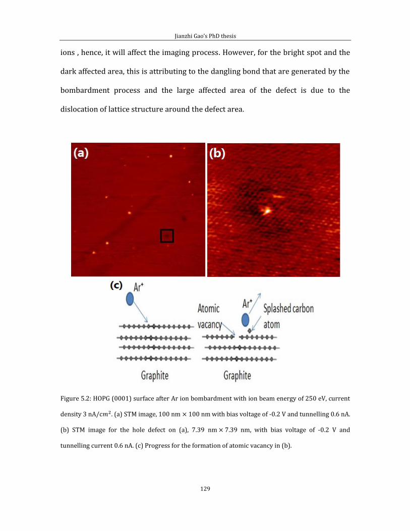
Jianzhi Gao’s PhD thesis
129
ions , hence, it will affect the imaging process. However, for the bright spot and the
dark affected area, this is attributing to the dangling bond that are generated by the
bombardment process and the large affected area of the defect is due to the
dislocation of lattice structure around the defect area.
Figure 5.2: HOPG (0001) surface after Ar ion bombardment with ion beam energy of 250 eV, current
density 3 nA/c . (a) STM image, 100 nm 100 nm with bias voltage of -0.2 V and tunnelling 0.6 nA.
(b) STM image for the hole defect on (a), 7.39 nm 7.39 nm, with bias voltage of -0.2 V and
tunnelling current 0.6 nA. (c) Progress for the formation of atomic vacancy in (b).
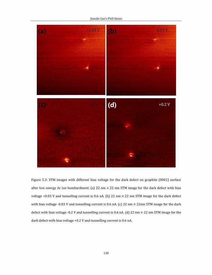
Jianzhi Gao’s PhD thesis
130
Figure 5.3: STM images with different bias voltage for the dark defect on graphite (0001) surface
after low energy Ar ion bombardment. (a) 22 nm 22 nm STM image for the dark defect with bias
voltage +0.03 V and tunnelling current is 0.6 nA. (b) 22 nm 22 nm STM image for the dark defect
with bias voltage -0.03 V and tunnelling current is 0.6 nA. (c) 22 nm 22nm STM image for the dark
defect with bias voltage -0.2 V and tunnelling current is 0.6 nA. (d) 22 nm 22 nm STM image for the
dark defect with bias voltage +0.2 V and tunnelling current is 0.6 nA.
+0.03 V -0.03 V
-0.2 V +0.2 V
Jianzhi Gao’s PhD thesis
131
Figure 5.2 (c) presents a schematic diagram showing the process of vacancy
formation. From figure 5.1 and 5.2, we know that vacancy defects show bias
dependent brightness, therefore, we did a series of experiment by imaging two
defects by changing the bias voltage in a systematic manner, which is shown in
figure 5.3.
Figure 5.3 shows the appearance of the two defects under different bias voltages.
For very low bias voltages, 0.03 V, the defects appear the same for both positive
and negative polarities. As the magnitude of the bias voltage is increased to 0.2 V, a
clear bright-dark contrast switch is observed. When the sample bias is positive,
atomic vacancy are bright as shown in figure 5.3 (d) (the upper defect in the STM
image). It becomes dark in the STM image when the sample bias is negative as
shown in figure 5.3 (c). This switching process can be observed with bias voltage
from 0.2 to 1.0 V, and it is not affected by the magnitude of the tunnel current. Choi
et al studied trapping of atoms during the low energy (10-600 eV) noble gas ion
bombardment on the graphite surface. (From figure 2.32 shown in chapter 2, Ion
beam with the high energy will destroy the surface structure of the graphite surface).
Argon atoms are released from the graphite surface when the sample is heated to
500 K to 600 K. Therefore, we have increased the substrate temperature to 1000 K
for 30 min. to drive out the trapped Ar.
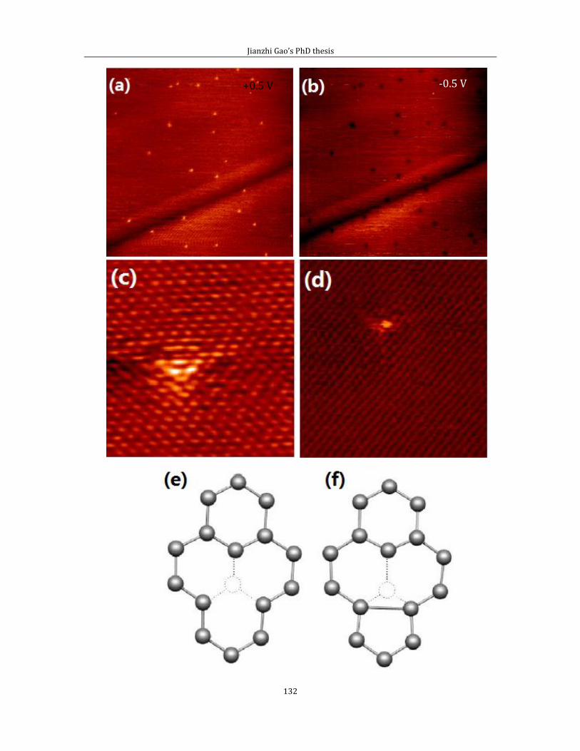
Jianzhi Gao’s PhD thesis
132
+0.5 V -0.5 V
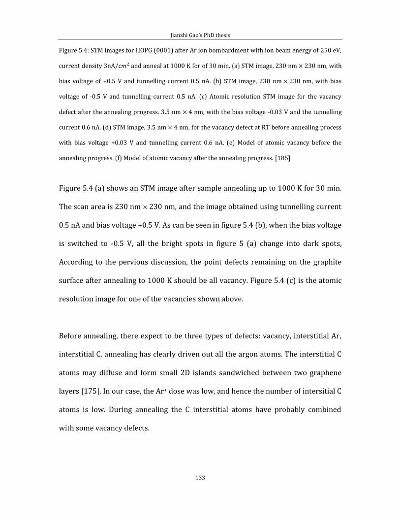
Jianzhi Gao’s PhD thesis
133
Figure 5.4: STM images for HOPG (0001) after Ar ion bombardment with ion beam energy of 250 eV,
current density 3nA/c and anneal at 1000 K for of 30 min. (a) STM image, 230 nm 230 nm, with
bias voltage of +0.5 V and tunnelling current 0.5 nA. (b) STM image, 230 nm 230 nm, with bias
voltage of -0.5 V and tunnelling current 0.5 nA. (c) Atomic resolution STM image for the vacancy
defect after the annealing progress. 3.5 nm 4 nm, with the bias voltage -0.03 V and the tunnelling
current 0.6 nA. (d) STM image, 3.5 nm 4 nm, for the vacancy defect at RT before annealing process
with bias voltage +0.03 V and tunnelling current 0.6 nA. (e) Model of atomic vacancy before the
annealing progress. (f) Model of atomic vacancy after the annealing progress. [185]
Figure 5.4 (a) shows an STM image after sample annealing up to 1000 K for 30 min.
The scan area is 230 nm 230 nm, and the image obtained using tunnelling current
0.5 nA and bias voltage +0.5 V. As can be seen in figure 5.4 (b), when the bias voltage
is switched to -0.5 V, all the bright spots in figure 5 (a) change into dark spots,
According to the pervious discussion, the point defects remaining on the graphite
surface after annealing to 1000 K should be all vacancy. Figure 5.4 (c) is the atomic
resolution image for one of the vacancies shown above.
Before annealing, there expect to be three types of defects: vacancy, interstitial Ar,
interstitial C. annealing has clearly driven out all the argon atoms. The interstitial C
atoms may diffuse and form small 2D islands sandwiched between two graphene
layers [175]. In our case, the Ar+ dose was low, and hence the number of intersitial C
atoms is low. During annealing the C interstitial atoms have probably combined
with some vacancy defects.
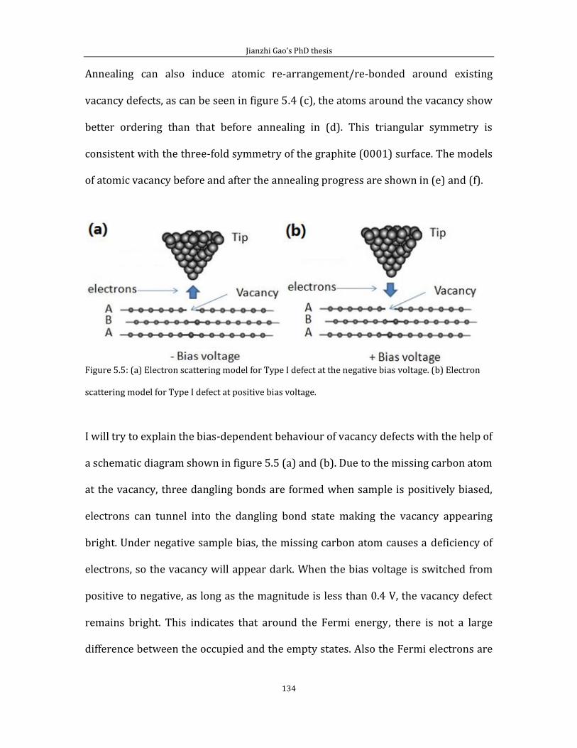
Jianzhi Gao’s PhD thesis
134
Annealing can also induce atomic re-arrangement/re-bonded around existing
vacancy defects, as can be seen in figure 5.4 (c), the atoms around the vacancy show
better ordering than that before annealing in (d). This triangular symmetry is
consistent with the three-fold symmetry of the graphite (0001) surface. The models
of atomic vacancy before and after the annealing progress are shown in (e) and (f).
Figure 5.5: (a) Electron scattering model for Type I defect at the negative bias voltage. (b) Electron
scattering model for Type I defect at positive bias voltage.
I will try to explain the bias-dependent behaviour of vacancy defects with the help of
a schematic diagram shown in figure 5.5 (a) and (b). Due to the missing carbon atom
at the vacancy, three dangling bonds are formed when sample is positively biased,
electrons can tunnel into the dangling bond state making the vacancy appearing
bright. Under negative sample bias, the missing carbon atom causes a deficiency of
electrons, so the vacancy will appear dark. When the bias voltage is switched from
positive to negative, as long as the magnitude is less than 0.4 V, the vacancy defect
remains bright. This indicates that around the Fermi energy, there is not a large
difference between the occupied and the empty states. Also the Fermi electrons are
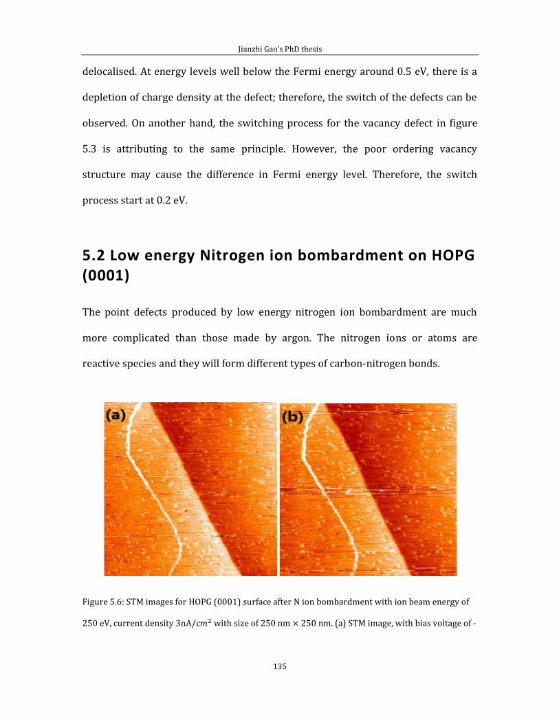
Jianzhi Gao’s PhD thesis
135
delocalised. At energy levels well below the Fermi energy around 0.5 eV, there is a
depletion of charge density at the defect; therefore, the switch of the defects can be
observed. On another hand, the switching process for the vacancy defect in figure
5.3 is attributing to the same principle. However, the poor ordering vacancy
structure may cause the difference in Fermi energy level. Therefore, the switch
process start at 0.2 eV.
5.2 Low energy Nitrogen ion bombardment on HOPG (0001)
The point defects produced by low energy nitrogen ion bombardment are much
more complicated than those made by argon. The nitrogen ions or atoms are
reactive species and they will form different types of carbon-nitrogen bonds.
Figure 5.6: STM images for HOPG (0001) surface after N ion bombardment with ion beam energy of
250 eV, current density 3nA/c with size of 250 nm 250 nm. (a) STM image, with bias voltage of -
Jianzhi Gao’s PhD thesis
136
0.5 V and tunnelling of 0.5 nA. (b) STM image, with bias voltage of +0.5 V and tunnelling of current
0.5 nA. (The dark dots are due to the poor resolution.)
Figure 5.6 shows STM images for the graphite (0001) surface after low energy
nitrogen ion bombardment. The ion flux is estimated to be 3 nA/c . The bright
spots randomly distributed in the images in figure 5.6 (a) and (b) are the point
defects produced by nitrogen implantation, and the white line in the image is a grain
boundary on HOPG (0001). There is also a step edge at the right side of the grain
boundary. The bright spots in the images can be due to the following: vacancy
defects as that created by Ar+ bombardment; interstitials of N or C; N atoms bonded
to C on the surface. High-resolution STM images for the point defects after the low
energy nitrogen ion bombardment are shown in figure 5.7. The defect shown in this
figure is chosen from those shown in figure 5.6.
All four images in figure 5.7 show the same defect imaged with different bias voltage.
We can see from these images that there is no damage to the top layer graphite
lattice. The defect is featured by a single atom showing the highest local charge
density of states in the black circle and showing the paralle atomic line structure ( In
(a)). Therefore, we assume this is an interstitoial N atom bridging the top two layers
of carbon. This N has penetrated the top layer of graphite as a charged N+, it is then
neutralised, and forms chemical bond with carbon atoms. This chemical bonding
modifies the local density of states. As noticed in figure 5.7, the group of bright
carbon atoms keeps on re-grouping during scanning. This is probably caused by the
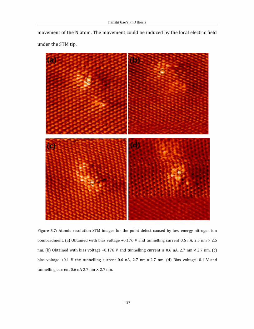
Jianzhi Gao’s PhD thesis
137
movement of the N atom. The movement could be induced by the local electric field
under the STM tip.
Figure 5.7: Atomic resolution STM images for the point defect caused by low energy nitrogen ion
bombardment. (a) Obtained with bias voltage +0.176 V and tunnelling current 0.6 nA, 2.5 nm 2.5
nm. (b) Obtained with bias voltage +0.176 V and tunnelling current is 0.6 nA, 2.7 nm 2.7 nm. (c)
bias voltage +0.1 V the tunnelling current 0.6 nA, 2.7 nm 2.7 nm. (d) Bias voltage -0.1 V and
tunnelling current 0.6 nA 2.7 nm 2.7 nm.
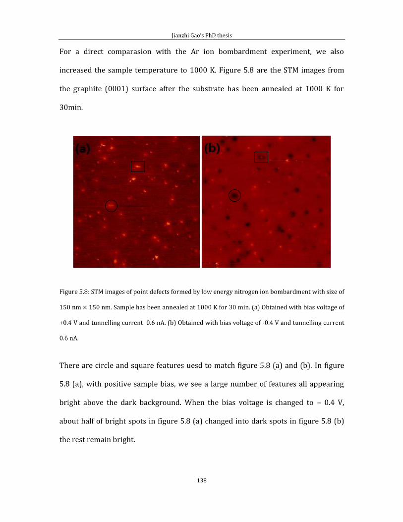
Jianzhi Gao’s PhD thesis
138
For a direct comparasion with the Ar ion bombardment experiment, we also
increased the sample temperature to 1000 K. Figure 5.8 are the STM images from
the graphite (0001) surface after the substrate has been annealed at 1000 K for
30min.
Figure 5.8: STM images of point defects formed by low energy nitrogen ion bombardment with size of
150 nm 150 nm. Sample has been annealed at 1000 K for 30 min. (a) Obtained with bias voltage of
+0.4 V and tunnelling current 0.6 nA. (b) Obtained with bias voltage of -0.4 V and tunnelling current
0.6 nA.
There are circle and square features uesd to match figure 5.8 (a) and (b). In figure
5.8 (a), with positive sample bias, we see a large number of features all appearing
bright above the dark background. When the bias voltage is changed to – 0.4 V,
about half of bright spots in figure 5.8 (a) changed into dark spots in figure 5.8 (b)
the rest remain bright.
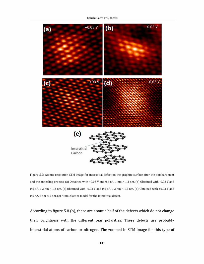
Jianzhi Gao’s PhD thesis
139
Figure 5.9: Atomic resolution STM image for interstitial defect on the graphite surface after the bombardment
and the annealing process. (a) Obtained with +0.03 V and 0.6 nA, 1 nm 1.2 nm. (b) Obtained with -0.03 V and
0.6 nA, 1.2 nm 1.2 nm. (c) Obtained with -0.03 V and 0.6 nA, 1.2 nm 1.5 nm. (d) Obtained with +0.03 V and
0.6 nA, 6 nm 5 nm. (e) Atomic lattice model for the interstitial defect.
According to figure 5.8 (b), there are about a half of the defects which do not change
their brightness with the different bias polarities. These defects are probably
interstitial atoms of carbon or nitrogen. The zoomed in STM image for this type of
+0.03 V -0.03 V
-0.03 V +0.03 V
Jianzhi Gao’s PhD thesis
140
defect is shown in figure 5.9. Figures 5.9 (a) to (d) are four differen interstitial
defects from figure 5.8 (b). We can see clearly from those images, this kind of defects
are linked to a small group of bright atoms without showing surface damage. Figure
5.9 (e) is the atomic lattice model for this type of defect. Based on appearance of the
STM images, it is not possible to separate carbon interstitials from nitrogen
interstitials. Apart from vacancy and interstitial defects there are other types of
defects casued by nitrogen. In the following, I will describe another two types of
defects.
Substitutional Doping of nitrogen Figure 5.10 shows a series of STM images from the same area, collected with
different bias voltages. The circles and squares are used to match the two different
defect features, where squares indicate the unchanged defects and circles indicate
the changing defects. In figure 5.10 (a), there is an interstitial defect observed at +
0.03 V sample boas. When the bias voltage is change to -0.03 V in figure 5.10 (b), the
image remains more or less the same with +0.03 V sample bias, figure 5.10 (c) a new
feature appears just above the interstitial defect indicated by a circle when we
compare to figure 5.10 (a) and (b). This new feature shows an interesting behaviour
as the bias voltage is changed to +0.1 V in figure 5.10 (d). In figure 5.10 (e), where
bias voltage is -0.2 V, this new feature looks quite bright. It turns deem when +0.2 V
is used in figure 5.10 (f). The same phenomena is observed at 0.5 V sample bias in
figure 5.10 (g) and (h). When the magnitude of the bias voltage is increased to 0.8 V,
we notice that the feature is bright at -0.8 V, but relatively deem at +0.8 V.
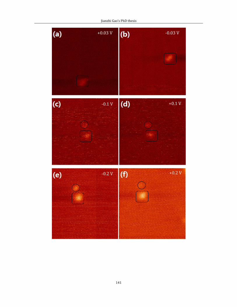
Jianzhi Gao’s PhD thesis
141
+0.03 V -0.03 V
-0.1 V +0.1 V
+0.2 V -0.2 V
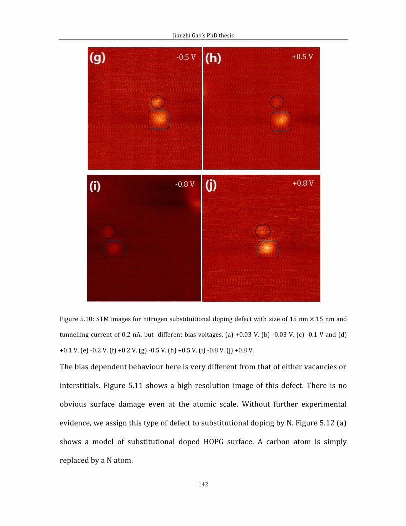
Jianzhi Gao’s PhD thesis
142
Figure 5.10: STM images for nitrogen substituitional doping defect with size of 15 nm 15 nm and
tunnelling current of 0.2 nA. but different bias voltages. (a) +0.03 V. (b) -0.03 V. (c) -0.1 V and (d)
+0.1 V. (e) -0.2 V. (f) +0.2 V. (g) -0.5 V. (h) +0.5 V. (i) -0.8 V. (j) +0.8 V.
The bias dependent behaviour here is very different from that of either vacancies or
interstitials. Figure 5.11 shows a high-resolution image of this defect. There is no
obvious surface damage even at the atomic scale. Without further experimental
evidence, we assign this type of defect to substitutional doping by N. Figure 5.12 (a)
shows a model of substitutional doped HOPG surface. A carbon atom is simply
replaced by a N atom.
-0.5 V +0.5 V
+0.8 V -0.8 V
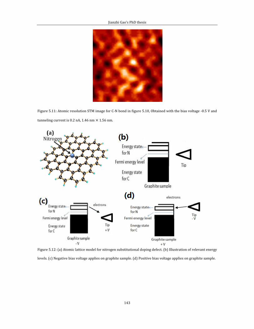
Jianzhi Gao’s PhD thesis
143
Figure 5.11: Atomic resolution STM image for C-N bond in figure 5.10, Obtained with the bias voltage -0.5 V and
tunneling current is 0.2 nA, 1.46 nm 1.56 nm.
Figure 5.12: (a) Atomic lattice model for nitrogen substitutional doping defect. (b) Illustration of relevant energy
levels. (c) Negative bias voltage applies on graphite sample. (d) Positive bias voltage applies on graphite sample.
Jianzhi Gao’s PhD thesis
144
Figure 5.12 (a) illustrate the nitrogen substitutional doping defect on HOPG (0001).
Using the schematic diagrams in figures 5.12 (b) to (d), we can explain the bias
dependent behaviour in a similar way as that used for doped semiconductors. The
substitutional of N provide an extra electron to the substrate. This electron occupies
the donor state which between the Fermi level and the conduction band. For
negative sample bias, electrons from the donor level can tunnel into the tip. If the
donor electron remains in the vicinity of the dopant then a small area around the N
dopant will appear bright. For positive sample bias, electrons from the tip must find
empty state in the sample for effective tunnelling around the N atom, the presence
of the donor electron makes the empty states partially filled.
Figure 5.13 shows the defect changing from atomic vacancy to nitrogen dome-like
structure, (a) and (b) show that the circled defects showing typical three-fold
symmetry and they turn into dark features when we apply the negative bias voltage.
Those defects were assigned to the atomic vacancies. However, after several rounds
of scanning and doing several times STS, those defects changed their feature. It
shows the circlar symmetry and decreases the affective area when we apply the
negative bias voltage in (b) and (c), which is completely different as the atomic
vacancy.
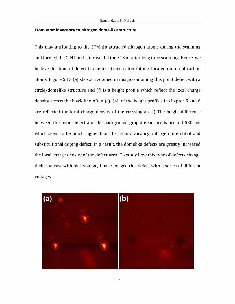
Jianzhi Gao’s PhD thesis
145
From atomic vacancy to nitrogen dome-like structure
This may attributing to the STM tip attracted nitrogen atoms during the scanning
and formed the C-N bond after we did the STS or after long time scanning. Hence, we
believe this kind of defect is due to nitrogen atom/atoms located on top of carbon
atoms. Figure 5.13 (e) shows a zoomed in image containing this point defect with a
circle/domelike structure and (f) is a height profile which reflect the local charge
density across the black line AB in (c). (All of the height profiles in chapter 5 and 6
are reflected the local charge density of the crossing area.) The height difference
between the point defect and the background graphite surface is around 530 pm
which seem to be much higher than the atomic vacancy, nitrogen interstitial and
substituitional doping defect. In a result, the domelike defects are greatly increased
the local charge density of the defect area. To study how this type of defects change
their contrast with bias voltage, I have imaged this defect with a series of different
voltages.
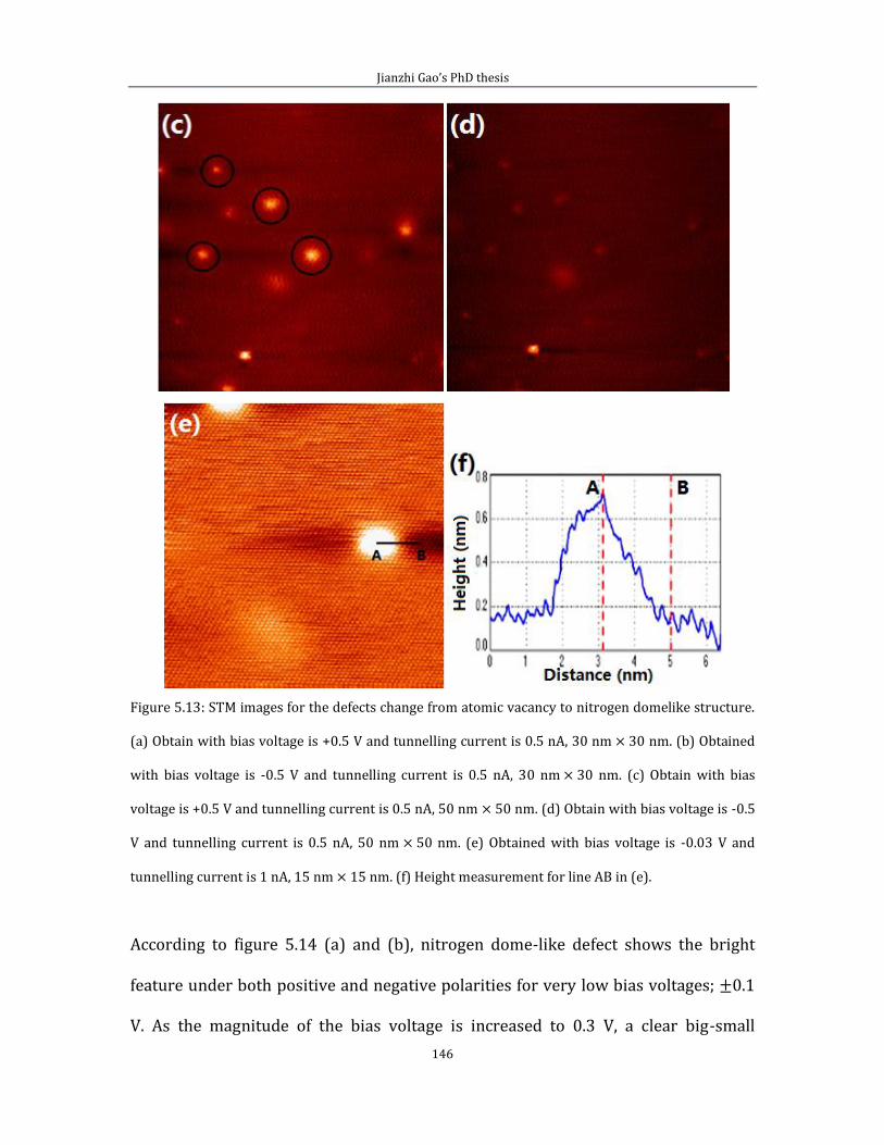
Jianzhi Gao’s PhD thesis
146
Figure 5.13: STM images for the defects change from atomic vacancy to nitrogen domelike structure.
(a) Obtain with bias voltage is +0.5 V and tunnelling current is 0.5 nA, 30 nm 30 nm. (b) Obtained
with bias voltage is -0.5 V and tunnelling current is 0.5 nA, 30 nm 30 nm. (c) Obtain with bias
voltage is +0.5 V and tunnelling current is 0.5 nA, 50 nm 50 nm. (d) Obtain with bias voltage is -0.5
V and tunnelling current is 0.5 nA, 50 nm 50 nm. (e) Obtained with bias voltage is -0.03 V and
tunnelling current is 1 nA, 15 nm 15 nm. (f) Height measurement for line AB in (e).
According to figure 5.14 (a) and (b), nitrogen dome-like defect shows the bright
feature under both positive and negative polarities for very low bias voltages; 0
V. As the magnitude of the bias voltage is increased to 0.3 V, a clear big-small
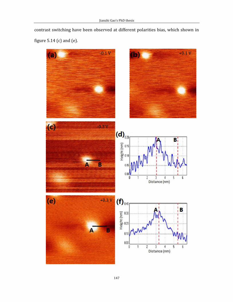
Jianzhi Gao’s PhD thesis
147
contrast switching have been observed at different polarities bias, which shown in
figure 5.14 (c) and (e).
+0.3 V
-0.3 V
-0.1 V +0.1 V
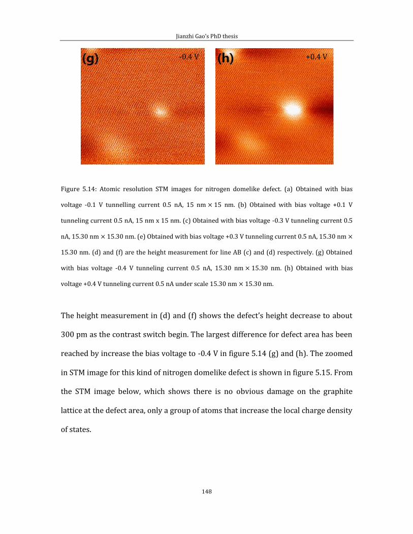
Jianzhi Gao’s PhD thesis
148
Figure 5.14: Atomic resolution STM images for nitrogen domelike defect. (a) Obtained with bias
voltage -0.1 V tunnelling current 0.5 nA, 15 nm 15 nm. (b) Obtained with bias voltage +0.1 V
tunneling current 0.5 nA, 15 nm x 15 nm. (c) Obtained with bias voltage -0.3 V tunneling current 0.5
nA, 15.30 nm 15.30 nm. (e) Obtained with bias voltage +0.3 V tunneling current 0.5 nA, 15.30 nm
15.30 nm. (d) and (f) are the height measurement for line AB (c) and (d) respectively. (g) Obtained
with bias voltage -0.4 V tunneling current 0.5 nA, 15.30 nm 15.30 nm. (h) Obtained with bias
voltage +0.4 V tunneling current 0.5 nA under scale 15.30 nm 15.30 nm.
The height measurement in (d) and (f) shows the defect’s height decrease to about
300 pm as the contrast switch begin. The largest difference for defect area has been
reached by increase the bias voltage to -0.4 V in figure 5.14 (g) and (h). The zoomed
in STM image for this kind of nitrogen domelike defect is shown in figure 5.15. From
the STM image below, which shows there is no obvious damage on the graphite
lattice at the defect area, only a group of atoms that increase the local charge density
of states.
-0.4 V +0.4 V
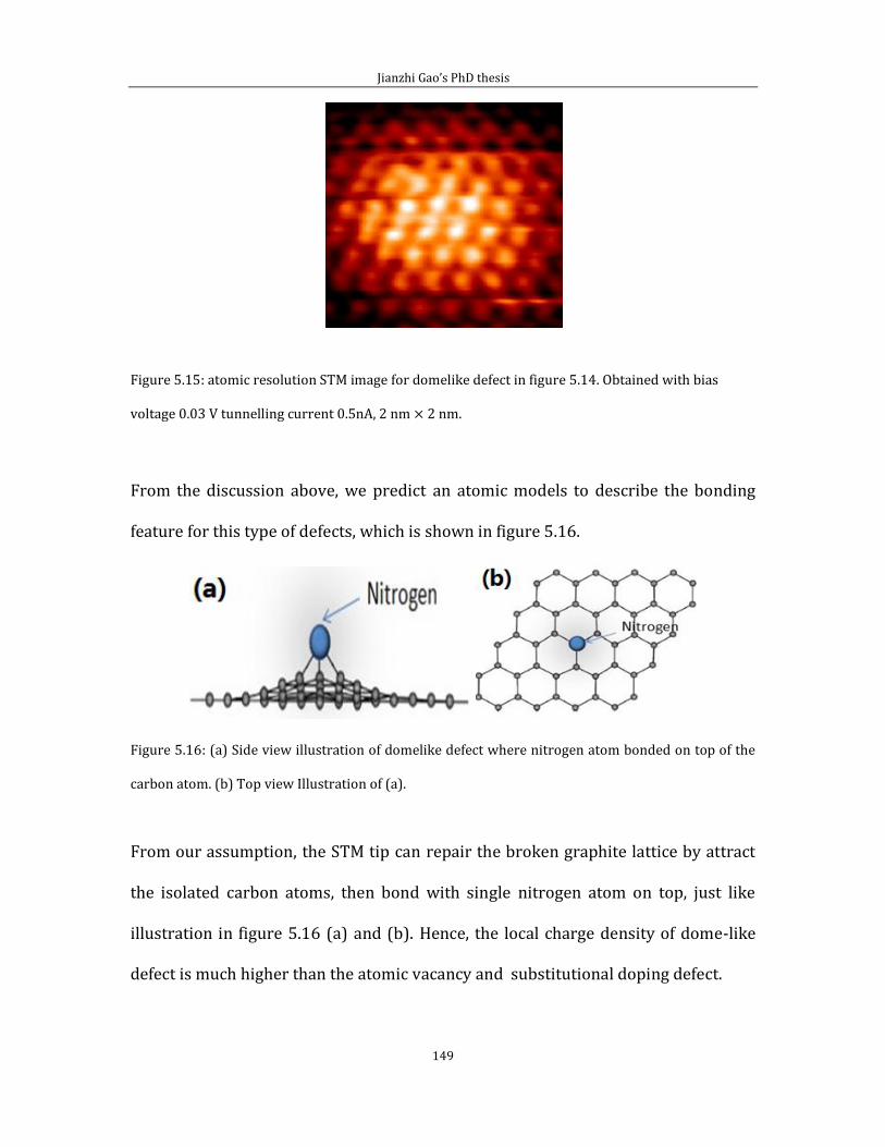
Jianzhi Gao’s PhD thesis
149
Figure 5.15: atomic resolution STM image for domelike defect in figure 5.14. Obtained with bias
voltage 0.03 V tunnelling current 0.5nA, 2 nm 2 nm.
From the discussion above, we predict an atomic models to describe the bonding
feature for this type of defects, which is shown in figure 5.16.
Figure 5.16: (a) Side view illustration of domelike defect where nitrogen atom bonded on top of the
carbon atom. (b) Top view Illustration of (a).
From our assumption, the STM tip can repair the broken graphite lattice by attract
the isolated carbon atoms, then bond with single nitrogen atom on top, just like
illustration in figure 5.16 (a) and (b). Hence, the local charge density of dome-like
defect is much higher than the atomic vacancy and substitutional doping defect.
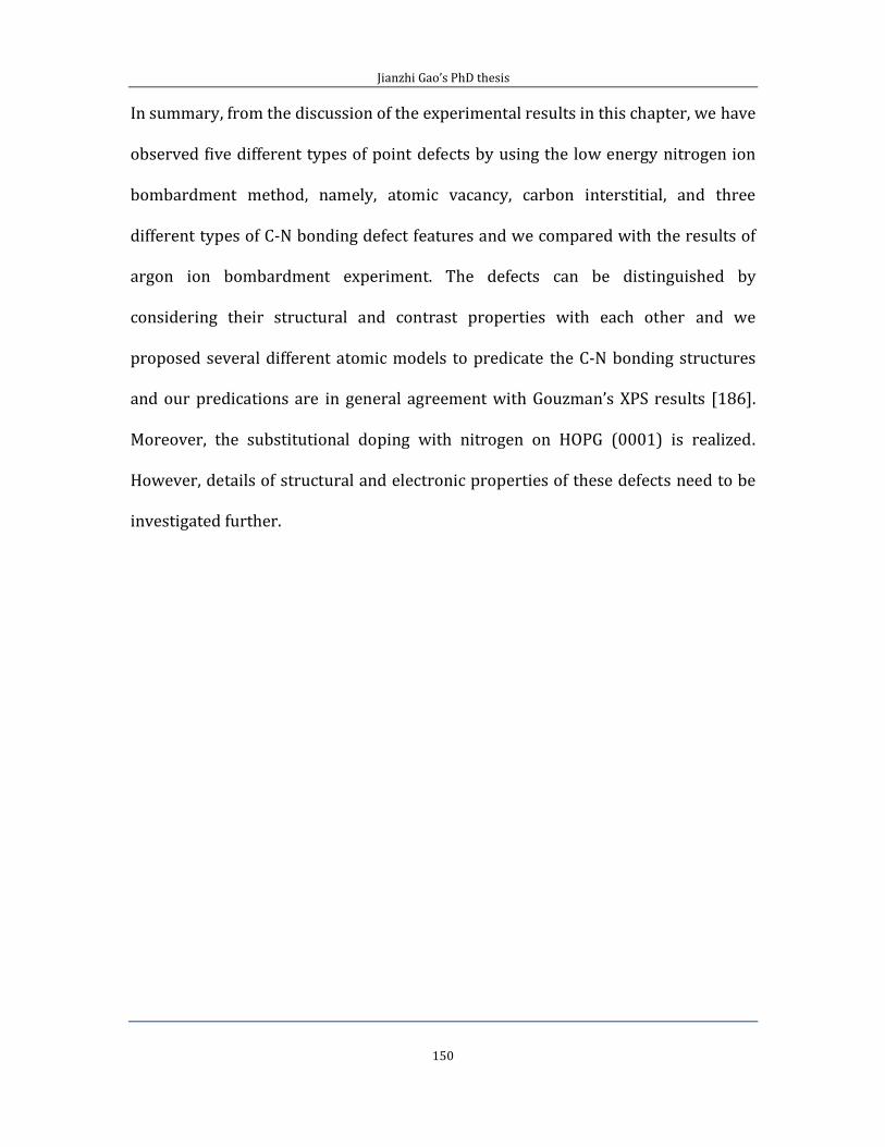
Jianzhi Gao’s PhD thesis
150
In summary, from the discussion of the experimental results in this chapter, we have
observed five different types of point defects by using the low energy nitrogen ion
bombardment method, namely, atomic vacancy, carbon interstitial, and three
different types of C-N bonding defect features and we compared with the results of
argon ion bombardment experiment. The defects can be distinguished by
considering their structural and contrast properties with each other and we
proposed several different atomic models to predicate the C-N bonding structures
and our predications are in general agreement with Gouzman’s XPS results [186].
Moreover, the substitutional doping with nitrogen on HOPG (0001) is realized.
However, details of structural and electronic properties of these defects need to be
investigated further.
Jianzhi Gao’s PhD thesis
151
Chapter 6 Thermally cracked atomic oxygen on HOPG (0001)
In the previous chapter, we discussed data from the experiment of low energy
Ar+/N+ bombardment of HOPG (0001). In this chapter, I will discuss, a related
process where atomic oxygen is added to HOPG.
6.1 Pinning platinum and Pt-oxide nanoparticles on graphite
Small metal clusters are widely used and take a significant position in the field of
heterogeneous catalysis [190,191]. Therefore, a large number of model systems are
used in order to study the fundamental mechanism of selectivity and reactivity of
supported metal catalysts. Among these, small metal particles on metal oxide
supports have been mostly studied and designed [192–196]. It was found in a very
early stage that the performance of the metal particles can be strongly influenced by
the metal-support interaction [197,198]. Moreover, the phenomenon of strong-
metal-support-interaction (SMSI) was extensively studied since it was discovered
[199–202]. To consider this situation, too strong an interaction from the metal oxide
support can cause the encapsulation of the metal, on the other hand, the weak
interaction would cause particles to sinter and hence the loss of the effective surface
area. Therefore, there is an optimizing solution of the metal support interaction that
are required to keep the metal particles catalytically active. Consequently, we come
up with a method to pin metal particles in our experimental study [203] to prevent
Jianzhi Gao’s PhD thesis
152
them from sintering.
We used the highly oriented pyrolitic graphite (HOPG) as the sample substrate. This
is because of its known inertness towards many metals. The interaction of metal
clusters/atoms with HOPG have been extensively studied in [204–216] especially
after the recent discovery of graphene [217–219].
Considering the unique physical properties of low diffusion barriers [204,205,207]
on HOPG, both individual atoms and clusters of metal are highly mobile on this
surface. Therefore, the deposited metal clusters or atoms tend to automatically
aggregate along the step edges of HOPG. Hence, prefabricated surface atomic defects
are required to fix metal clusters on HOPG. There are a number of experimental
methods to solve this problem, such as Ar+ ion sputtering on HOPG surface [212].
Also, there is an alternative method that impinge the metal clusters with high kinetic
energies onto the HOPG surface [209,214,215]. However, both of these methods can
cause physical damage to the graphite surface. To overcome this problem, we
developed a procedure in our experiment to fix Pt oxide particles without causing
extra physical damage to the HOPG substrate by using a heated Pt capillary tube.
The basic idea is to pass oxygen gas through the heated Pt capillary tube hence co-
deposit atomic oxygen and Pt oxide nanoparticles simultaneously. Moreover, the
defect features on the HOPG surface due to atomic oxygen are able to pin the Pt
metal oxide particles. Our experimental method for fixing Pt and PtO particles on
graphite to form graphite-supported Pt catalysts is a significant process for the fuel
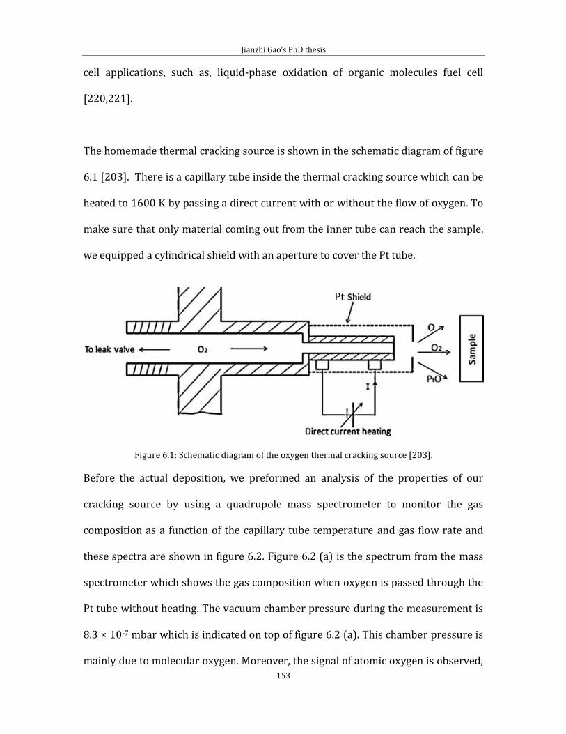
Jianzhi Gao’s PhD thesis
153
cell applications, such as, liquid-phase oxidation of organic molecules fuel cell
[220,221].
The homemade thermal cracking source is shown in the schematic diagram of figure
6.1 [203]. There is a capillary tube inside the thermal cracking source which can be
heated to 1600 K by passing a direct current with or without the flow of oxygen. To
make sure that only material coming out from the inner tube can reach the sample,
we equipped a cylindrical shield with an aperture to cover the Pt tube.
Figure 6.1: Schematic diagram of the oxygen thermal cracking source [203].
Before the actual deposition, we preformed an analysis of the properties of our
cracking source by using a quadrupole mass spectrometer to monitor the gas
composition as a function of the capillary tube temperature and gas flow rate and
these spectra are shown in figure 6.2. Figure 6.2 (a) is the spectrum from the mass
spectrometer which shows the gas composition when oxygen is passed through the
Pt tube without heating. The vacuum chamber pressure during the measurement is
8.3 × 10⁻⁷ mbar which is indicated on top of figure 6.2 (a). This chamber pressure is
mainly due to molecular oxygen. Moreover, the signal of atomic oxygen is observed,
Pt
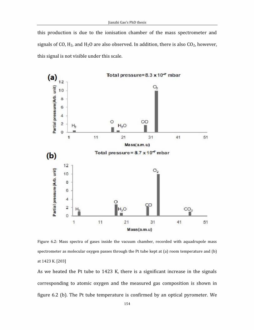
Jianzhi Gao’s PhD thesis
154
this production is due to the ionisation chamber of the mass spectrometer and
signals of CO, H2, and H2O are also observed. In addition, there is also CO2, however,
this signal is not visible under this scale.
Figure 6.2: Mass spectra of gases inside the vacuum chamber, recorded with aquadrupole mass
spectrometer as molecular oxygen passes through the Pt tube kept at (a) room temperature and (b)
at 1423 K. [203]
As we heated the Pt tube to 1423 K, there is a significant increase in the signals
corresponding to atomic oxygen and the measured gas composition is shown in
figure 6.2 (b). The Pt tube temperature is confirmed by an optical pyrometer. We
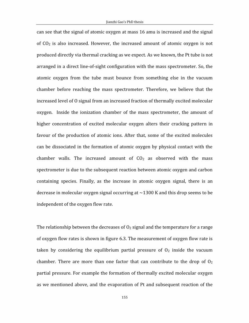
Jianzhi Gao’s PhD thesis
155
can see that the signal of atomic oxygen at mass 16 amu is increased and the signal
of CO2 is also increased. However, the increased amount of atomic oxygen is not
produced directly via thermal cracking as we expect. As we known, the Pt tube is not
arranged in a direct line-of-sight configuration with the mass spectrometer. So, the
atomic oxygen from the tube must bounce from something else in the vacuum
chamber before reaching the mass spectrometer. Therefore, we believe that the
increased level of O signal from an increased fraction of thermally excited molecular
oxygen. Inside the ionization chamber of the mass spectrometer, the amount of
higher concentration of excited molecular oxygen alters their cracking pattern in
favour of the production of atomic ions. After that, some of the excited molecules
can be dissociated in the formation of atomic oxygen by physical contact with the
chamber walls. The increased amount of CO2 as observed with the mass
spectrometer is due to the subsequent reaction between atomic oxygen and carbon
containing species. Finally, as the increase in atomic oxygen signal, there is an
decrease in molecular oxygen signal occurring at ∼1300 K and this drop seems to be
independent of the oxygen flow rate.
The relationship between the decreases of O2 signal and the temperature for a range
of oxygen flow rates is shown in figure 6.3. The measurement of oxygen flow rate is
taken by considering the equilibrium partial pressure of O2 inside the vacuum
chamber. There are more than one factor that can contribute to the drop of O2
partial pressure. For example the formation of thermally excited molecular oxygen
as we mentioned above, and the evaporation of Pt and subsequent reaction of the
Jianzhi Gao’s PhD thesis
156
molecular oxygen with evaporated Pt atoms. However, the consumption of O2 by
thermal cracking into atomic oxygen inside the Pt tube is the most obvious one.
What is more, it is not clear which of the three processes contributes most
consumption of molecular oxygen so far, but, Pt evaporation has indeed occurred as
shown by the STM measurement.
Figure 6.3: Partial pressure of O2 as a function of capillary tube temperature [203].
The following discussion is related to the STM work. The STM images of deposition
of Pt on the HOPG sample surface in the absence of oxygen are shown in figure 6.4.
For this part of the experiment, we heated the Pt tube to 1423 K and let its open end
facing the HOPG sample for a duration of 3 min inside UHV chamber. There is no
oxygen flowing through the Pt tube during the whole process and the STM images
were obtained after the HOPG sample cooling down to room temperature. The STM
image in figure 6.4 (a) shows the Pt particles have aggregated along the grain
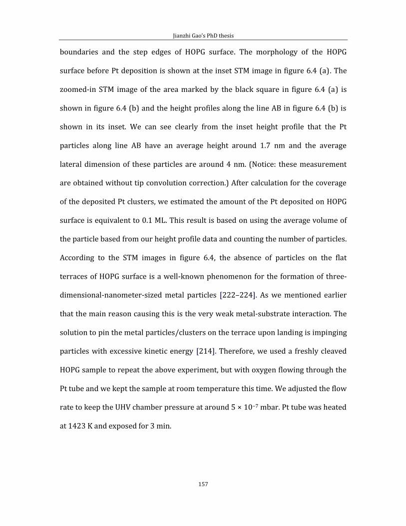
Jianzhi Gao’s PhD thesis
157
boundaries and the step edges of HOPG surface. The morphology of the HOPG
surface before Pt deposition is shown at the inset STM image in figure 6.4 (a). The
zoomed-in STM image of the area marked by the black square in figure 6.4 (a) is
shown in figure 6.4 (b) and the height profiles along the line AB in figure 6.4 (b) is
shown in its inset. We can see clearly from the inset height profile that the Pt
particles along line AB have an average height around 1.7 nm and the average
lateral dimension of these particles are around 4 nm. (Notice: these measurement
are obtained without tip convolution correction.) After calculation for the coverage
of the deposited Pt clusters, we estimated the amount of the Pt deposited on HOPG
surface is equivalent to 0.1 ML. This result is based on using the average volume of
the particle based from our height profile data and counting the number of particles.
According to the STM images in figure 6.4, the absence of particles on the flat
terraces of HOPG surface is a well-known phenomenon for the formation of three-
dimensional-nanometer-sized metal particles [222–224]. As we mentioned earlier
that the main reason causing this is the very weak metal-substrate interaction. The
solution to pin the metal particles/clusters on the terrace upon landing is impinging
particles with excessive kinetic energy [214]. Therefore, we used a freshly cleaved
HOPG sample to repeat the above experiment, but with oxygen flowing through the
Pt tube and we kept the sample at room temperature this time. We adjusted the flow
rate to keep the UHV chamber pressure at around 5 × 10⁻⁷ mbar. Pt tube was heated
at 1423 K and exposed for 3 min.
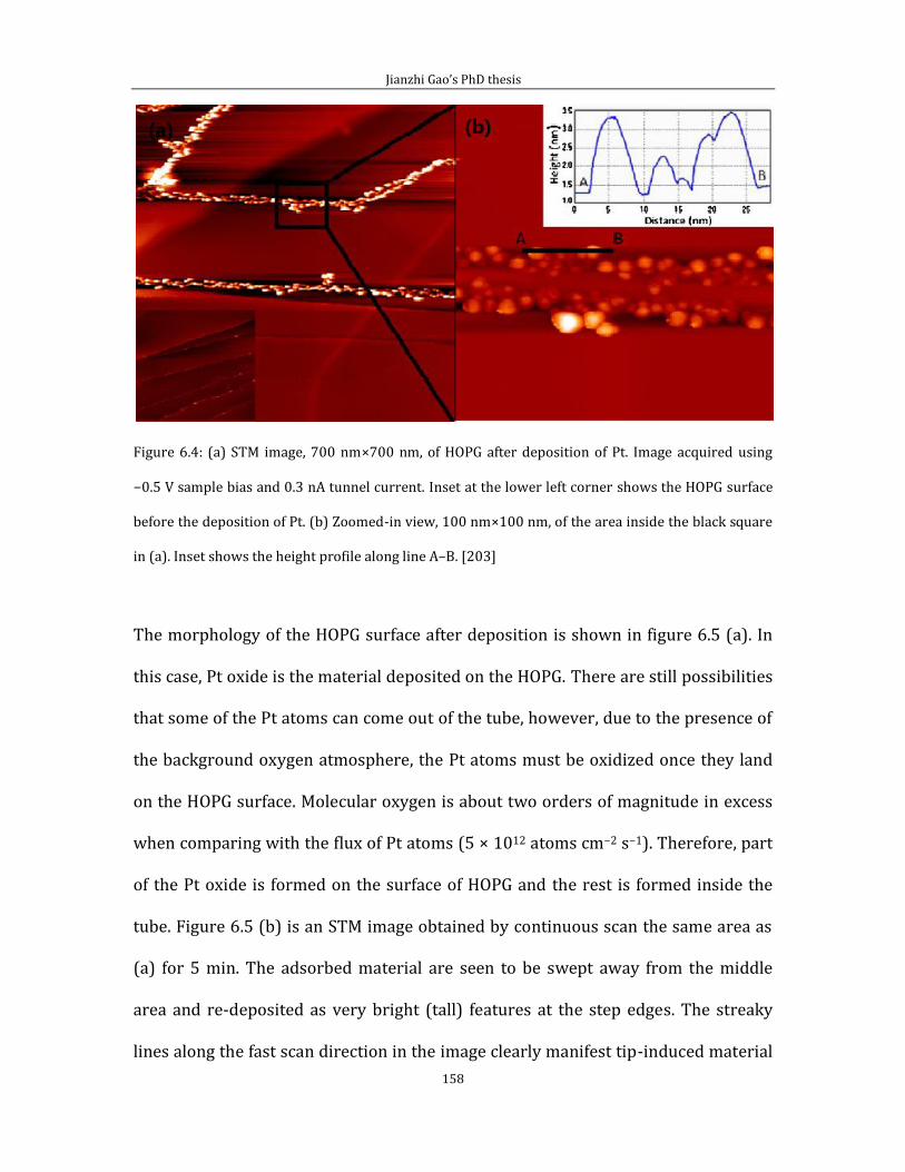
Jianzhi Gao’s PhD thesis
158
Figure 6.4: (a) STM image, 700 nm×700 nm, of HOPG after deposition of Pt. Image acquired using
−0.5 V sample bias and 0.3 nA tunnel current. Inset at the lower left corner shows the HOPG surface
before the deposition of Pt. (b) Zoomed-in view, 100 nm×100 nm, of the area inside the black square
in (a). Inset shows the height profile along line A–B. [203]
The morphology of the HOPG surface after deposition is shown in figure 6.5 (a). In
this case, Pt oxide is the material deposited on the HOPG. There are still possibilities
that some of the Pt atoms can come out of the tube, however, due to the presence of
the background oxygen atmosphere, the Pt atoms must be oxidized once they land
on the HOPG surface. Molecular oxygen is about two orders of magnitude in excess
when comparing with the flux of Pt atoms (5 × 10¹² atoms cm−2 s−1). Therefore, part
of the Pt oxide is formed on the surface of HOPG and the rest is formed inside the
tube. Figure 6.5 (b) is an STM image obtained by continuous scan the same area as
(a) for 5 min. The adsorbed material are seen to be swept away from the middle
area and re-deposited as very bright (tall) features at the step edges. The streaky
lines along the fast scan direction in the image clearly manifest tip-induced material
Jianzhi Gao’s PhD thesis
159
movement. An additional 5 min of scanning leads to the STM image shown in figure
6.5 (c). We can see that there is a increasing number of bright features along the
step edges. The zoomed-in STM image of the area inside the square box in (c) is
shown in figure 6.5 (d). The linear feature from top left to lower right is a mismatch
boundary between two grains of graphite. The small bright features are due to the
atomic oxygen attached to the carbon atoms on the top layer of HOPG and there may
some residual PtO. We annealed the sample at 473 K, 773 K and 973 K, 30 min at
each temperature in vacuum to evaluate the thermal stability of the oxide particles
and the obtained STM images are shown in figure 6.6.
Figure 6.6 (a) was obtained after annealing to 473 K. we can see that the small
particles have become stabilized. Figure 6.6 (b) was obtained after annealing to 773
K. We can see that there are a few relatively large fractal islands at the lower half of
the image in figure 6.6 (b) and the fractal islands consists of small particles. From a
recent study [224], nanoparticles of PtO supported on silica are stable up to 800 K.
Therefore, the fractal islands are still formed by the metal oxide particles. Pt metal
would form compact islands at this temperature [203]. However, the situation is
completely different after annealing the sample to 973 K as shown by the image in
figure 6.6 (c). According to figure 6.6 (c), only small bright spots and isolated
particles can be seen in the STM image.
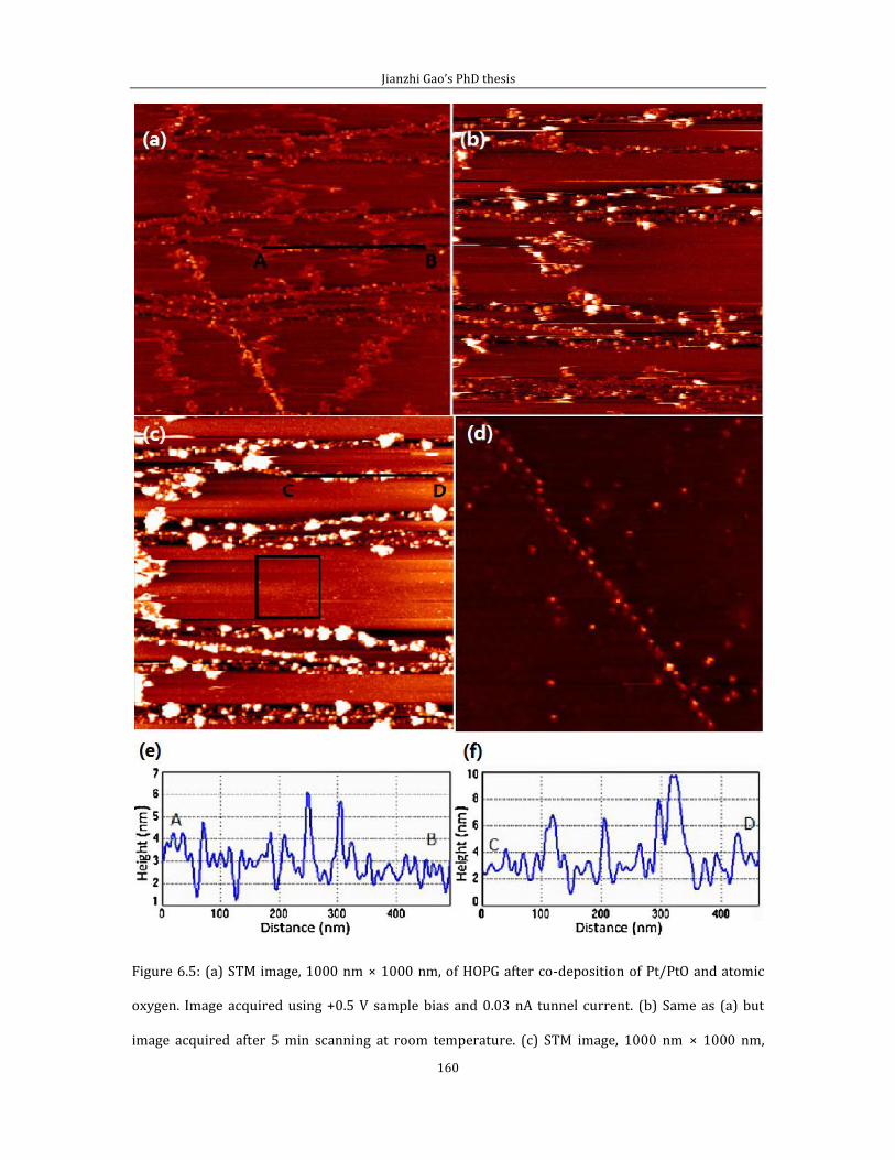
Jianzhi Gao’s PhD thesis
160
Figure 6.5: (a) STM image, 1000 nm × 1000 nm, of HOPG after co-deposition of Pt/PtO and atomic
oxygen. Image acquired using +0.5 V sample bias and 0.03 nA tunnel current. (b) Same as (a) but
image acquired after 5 min scanning at room temperature. (c) STM image, 1000 nm × 1000 nm,
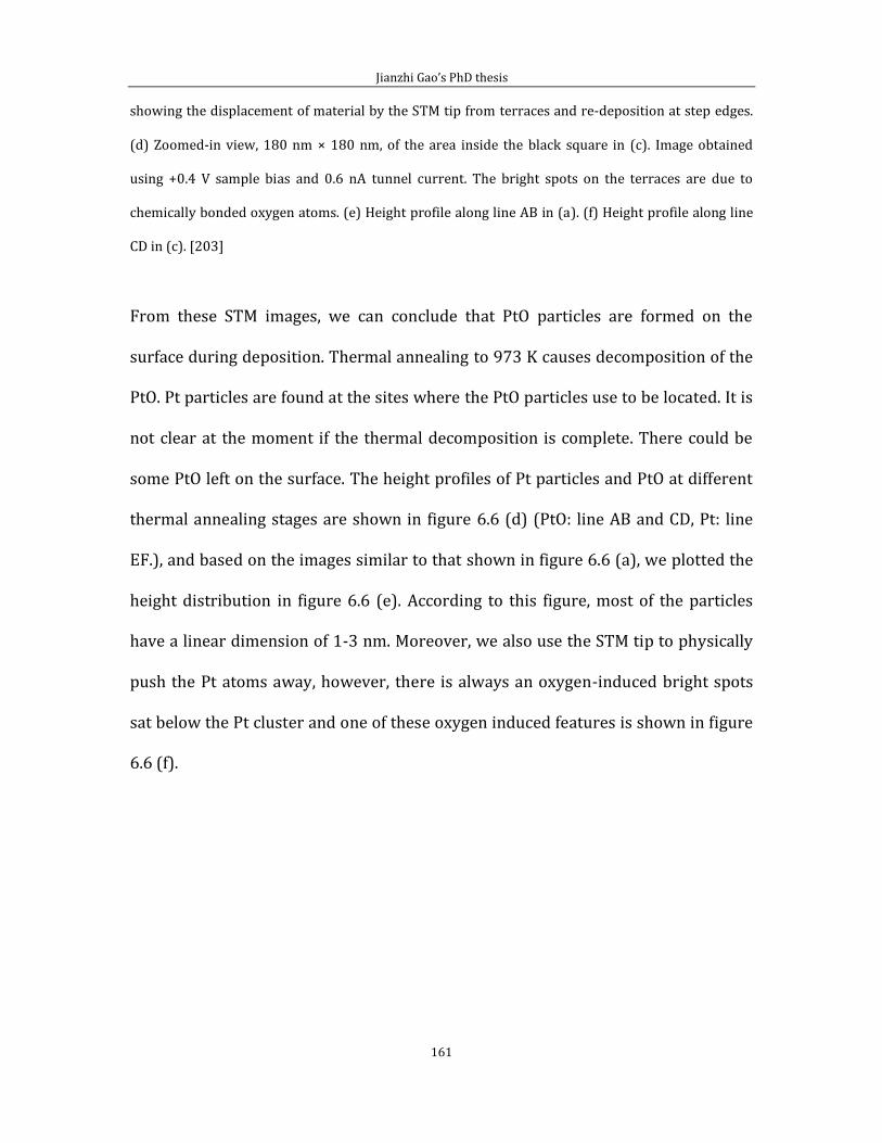
Jianzhi Gao’s PhD thesis
161
showing the displacement of material by the STM tip from terraces and re-deposition at step edges.
(d) Zoomed-in view, 180 nm × 180 nm, of the area inside the black square in (c). Image obtained
using +0.4 V sample bias and 0.6 nA tunnel current. The bright spots on the terraces are due to
chemically bonded oxygen atoms. (e) Height profile along line AB in (a). (f) Height profile along line
CD in (c). [203]
From these STM images, we can conclude that PtO particles are formed on the
surface during deposition. Thermal annealing to 973 K causes decomposition of the
PtO. Pt particles are found at the sites where the PtO particles use to be located. It is
not clear at the moment if the thermal decomposition is complete. There could be
some PtO left on the surface. The height profiles of Pt particles and PtO at different
thermal annealing stages are shown in figure 6.6 (d) (PtO: line AB and CD, Pt: line
EF.), and based on the images similar to that shown in figure 6.6 (a), we plotted the
height distribution in figure 6.6 (e). According to this figure, most of the particles
have a linear dimension of 1-3 nm. Moreover, we also use the STM tip to physically
push the Pt atoms away, however, there is always an oxygen-induced bright spots
sat below the Pt cluster and one of these oxygen induced features is shown in figure
6.6 (f).
Jianzhi Gao’s PhD thesis
162
Jianzhi Gao’s PhD thesis
163
Figure 6.6: (a) STM image, 1000 nm × 1000 nm, of HOPG with deposited PtO following thermal
annealing to 473 K in UHV. Image was obtained using −0.5 V sample bias and 0.03 nA tunnel current.
(b) The same sample after thermal annealing to 773 K. (c) The same sample after thermal annealing
to 973 K. (d) Height measurement across line AB, CD, and EF respectively. (e) Height distributing
statistics of (a). (f) Atomically resolved STM image obtained using −0.2 V sample bias and 0.8 nA
tunnel current, 3 nm × 3 nm, showing the detailed structure induced by the adsorption of atomic
oxygen. [203]
In summary, the binding of atomic oxygen to surface carbon atoms on HOPG creates
strong pinning sites where PtO particles are attached. Thermal annealing
experiments show that the PtO particles are stable up to 773 K. Higher temperature
causes thermal decomposition of the PtO, which leads to the formation of dispersed
metallic Pt particles at the initial pinning sites.
6.2 Binding of atomic oxygen to HOPG
In section 6.1, we have already mentioned the presence of atomic oxygen on HOPG.
In this section. I would like to describe finer details of oxygen induced structures on
HOPG.
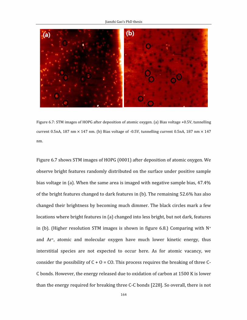
Jianzhi Gao’s PhD thesis
164
Figure 6.7: STM images of HOPG after deposition of atomic oxygen. (a) Bias voltage +0.5V, tunnelling
current 0.5nA, 187 nm 147 nm. (b) Bias voltage of -0.5V, tunnelling current 0.5nA, 187 nm 147
nm.
Figure 6.7 shows STM images of HOPG (0001) after deposition of atomic oxygen. We
observe bright features randomly distributed on the surface under positive sample
bias voltage in (a). When the same area is imaged with negative sample bias, 47.4%
of the bright features changed to dark features in (b). The remaining 52.6% has also
changed their brightness by becoming much dimmer. The black circles mark a few
locations where bright features in (a) changed into less bright, but not dark, features
in (b). (Higher resolution STM images is shown in figure 6.8.) Comparing with N+
and Ar+, atomic and molecular oxygen have much lower kinetic energy, thus
interstitial species are not expected to occur here. As for atomic vacancy, we
consider the possibility of C + O = CO. This process requires the breaking of three C-
C bonds. However, the energy released due to oxidation of carbon at 1500 K is lower
than the energy required for breaking three C-C bonds [228]. So overall, there is not
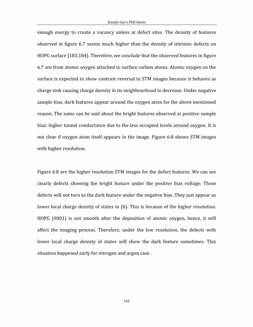
Jianzhi Gao’s PhD thesis
165
enough energy to create a vacancy unless at defect sites. The density of features
observed in figure 6.7 seems much higher than the density of intrinsic defects on
HOPG surface [183,184]. Therefore, we conclude that the observed features in figure
6.7 are from atomic oxygen attached to surface carbon atoms. Atomic oxygen on the
surface is expected to show contrast reversal in STM images because it behaves as
charge sink causing charge density in its neighbourhood to decrease. Under negative
sample bias, dark features appear around the oxygen atom for the above mentioned
reason. The same can be said about the bright features observed at positive sample
bias: higher tunnel conductance due to the less occupied levels around oxygen. It is
not clear if oxygen atom itself appears in the image. Figure 6.8 shows STM images
with higher resolution.
Figure 6.8 are the higher resolution STM images for the defect features. We can see
clearly defects showing the bright feature under the positive bias voltage. Those
defects will not turn to the dark feature under the negative bias. They just appear as
lower local charge density of states in (b). This is because of the higher resolution.
HOPG (0001) is not smooth after the deposition of atomic oxygen, hence, it will
affect the imaging process. Therefore, under the low resolution, the defects with
lower local charge density of states will show the dark feature sometimes. This
situation happened early for nitrogen and argon case .
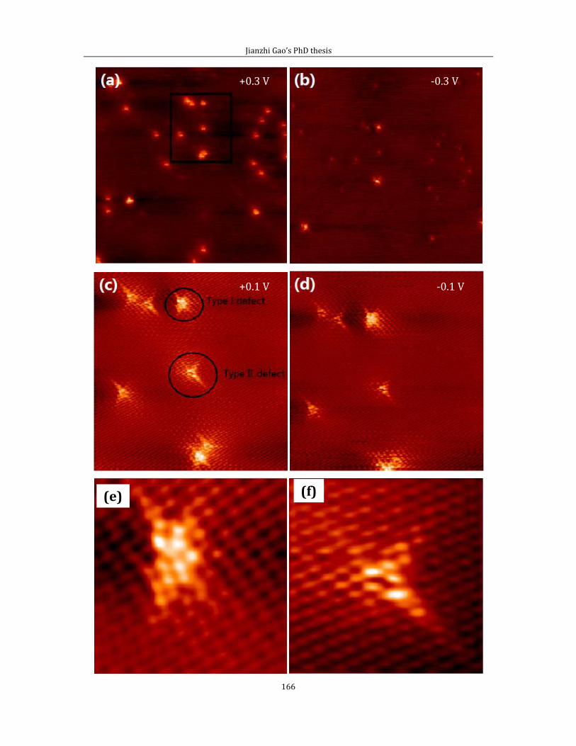
Jianzhi Gao’s PhD thesis
166
+0.3 V -0.3 V
+0.1 V -0.1 V
(f) (e)
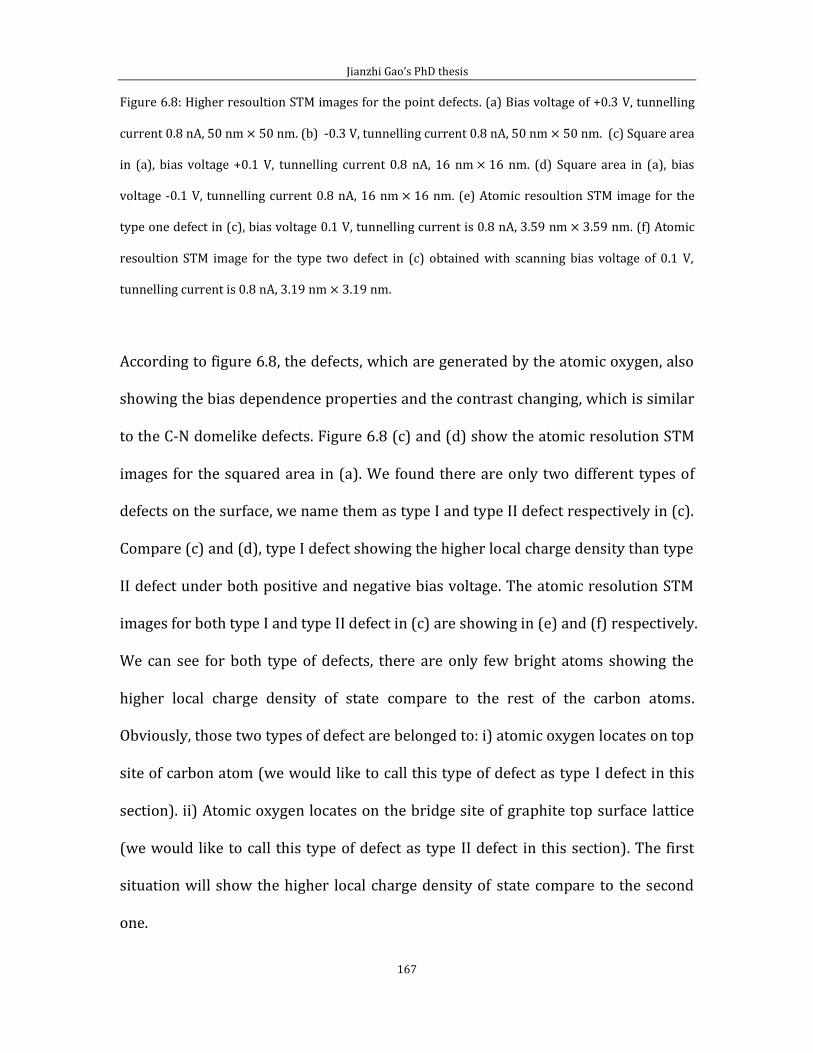
Jianzhi Gao’s PhD thesis
167
Figure 6.8: Higher resoultion STM images for the point defects. (a) Bias voltage of +0.3 V, tunnelling
current 0.8 nA, 50 nm 50 nm. (b) -0.3 V, tunnelling current 0.8 nA, 50 nm 50 nm. (c) Square area
in (a), bias voltage +0.1 V, tunnelling current 0.8 nA, 16 nm 16 nm. (d) Square area in (a), bias
voltage -0.1 V, tunnelling current 0.8 nA, 16 nm 16 nm. (e) Atomic resoultion STM image for the
type one defect in (c), bias voltage 0.1 V, tunnelling current is 0.8 nA, 3.59 nm 3.59 nm. (f) Atomic
resoultion STM image for the type two defect in (c) obtained with scanning bias voltage of 0.1 V,
tunnelling current is 0.8 nA, 3.19 nm 3.19 nm.
According to figure 6.8, the defects, which are generated by the atomic oxygen, also
showing the bias dependence properties and the contrast changing, which is similar
to the C-N domelike defects. Figure 6.8 (c) and (d) show the atomic resolution STM
images for the squared area in (a). We found there are only two different types of
defects on the surface, we name them as type I and type II defect respectively in (c).
Compare (c) and (d), type I defect showing the higher local charge density than type
II defect under both positive and negative bias voltage. The atomic resolution STM
images for both type I and type II defect in (c) are showing in (e) and (f) respectively.
We can see for both type of defects, there are only few bright atoms showing the
higher local charge density of state compare to the rest of the carbon atoms.
Obviously, those two types of defect are belonged to: i) atomic oxygen locates on top
site of carbon atom (we would like to call this type of defect as type I defect in this
section). ii) Atomic oxygen locates on the bridge site of graphite top surface lattice
(we would like to call this type of defect as type II defect in this section). The first
situation will show the higher local charge density of state compare to the second
one.
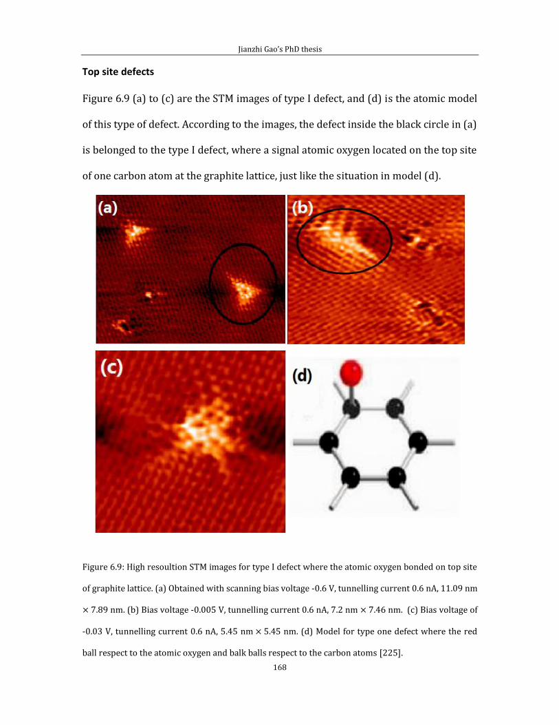
Jianzhi Gao’s PhD thesis
168
Top site defects
Figure 6.9 (a) to (c) are the STM images of type I defect, and (d) is the atomic model
of this type of defect. According to the images, the defect inside the black circle in (a)
is belonged to the type I defect, where a signal atomic oxygen located on the top site
of one carbon atom at the graphite lattice, just like the situation in model (d).
Figure 6.9: High resoultion STM images for type I defect where the atomic oxygen bonded on top site
of graphite lattice. (a) Obtained with scanning bias voltage -0.6 V, tunnelling current 0.6 nA, 11.09 nm
7.89 nm. (b) Bias voltage -0.005 V, tunnelling current 0.6 nA, 7.2 nm 7.46 nm. (c) Bias voltage of
-0.03 V, tunnelling current 0.6 nA, 5.45 nm 5.45 nm. (d) Model for type one defect where the red
ball respect to the atomic oxygen and balk balls respect to the carbon atoms [225].
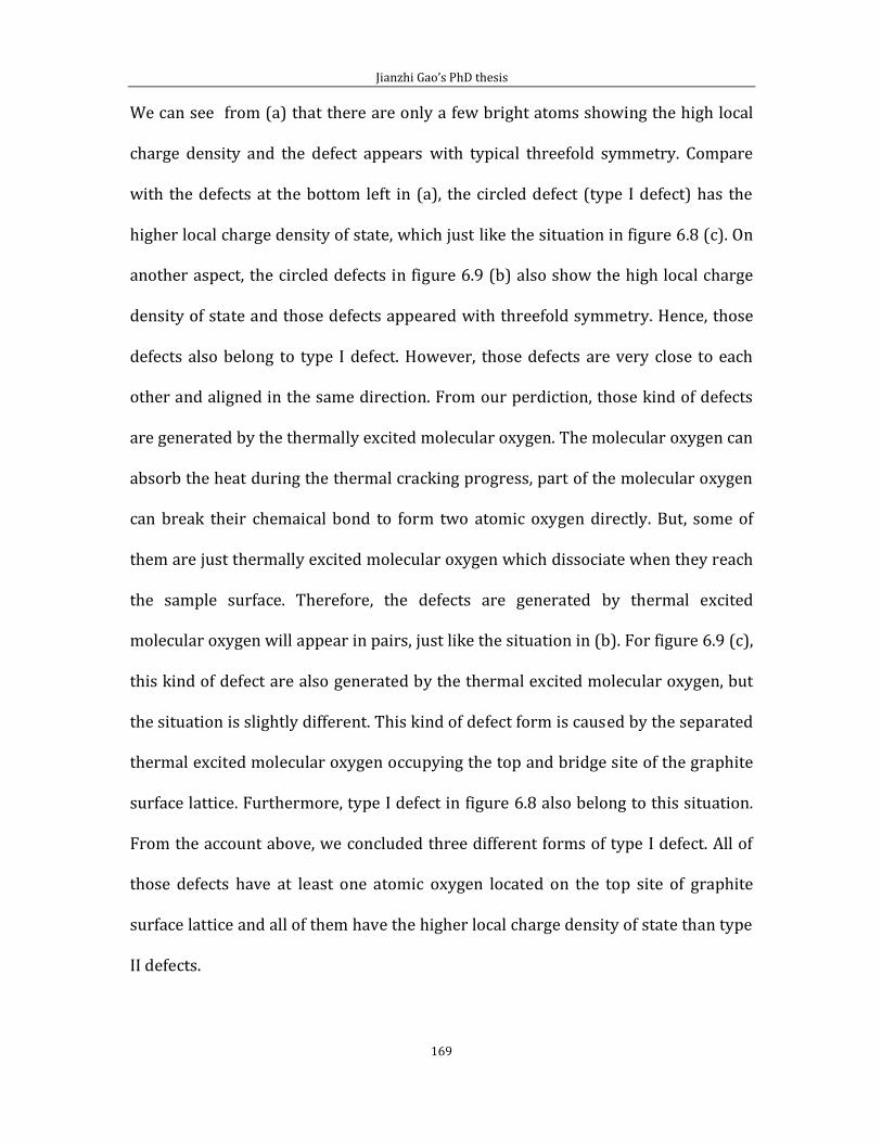
Jianzhi Gao’s PhD thesis
169
We can see from (a) that there are only a few bright atoms showing the high local
charge density and the defect appears with typical threefold symmetry. Compare
with the defects at the bottom left in (a), the circled defect (type I defect) has the
higher local charge density of state, which just like the situation in figure 6.8 (c). On
another aspect, the circled defects in figure 6.9 (b) also show the high local charge
density of state and those defects appeared with threefold symmetry. Hence, those
defects also belong to type I defect. However, those defects are very close to each
other and aligned in the same direction. From our perdiction, those kind of defects
are generated by the thermally excited molecular oxygen. The molecular oxygen can
absorb the heat during the thermal cracking progress, part of the molecular oxygen
can break their chemaical bond to form two atomic oxygen directly. But, some of
them are just thermally excited molecular oxygen which dissociate when they reach
the sample surface. Therefore, the defects are generated by thermal excited
molecular oxygen will appear in pairs, just like the situation in (b). For figure 6.9 (c),
this kind of defect are also generated by the thermal excited molecular oxygen, but
the situation is slightly different. This kind of defect form is caused by the separated
thermal excited molecular oxygen occupying the top and bridge site of the graphite
surface lattice. Furthermore, type I defect in figure 6.8 also belong to this situation.
From the account above, we concluded three different forms of type I defect. All of
those defects have at least one atomic oxygen located on the top site of graphite
surface lattice and all of them have the higher local charge density of state than type
II defects.
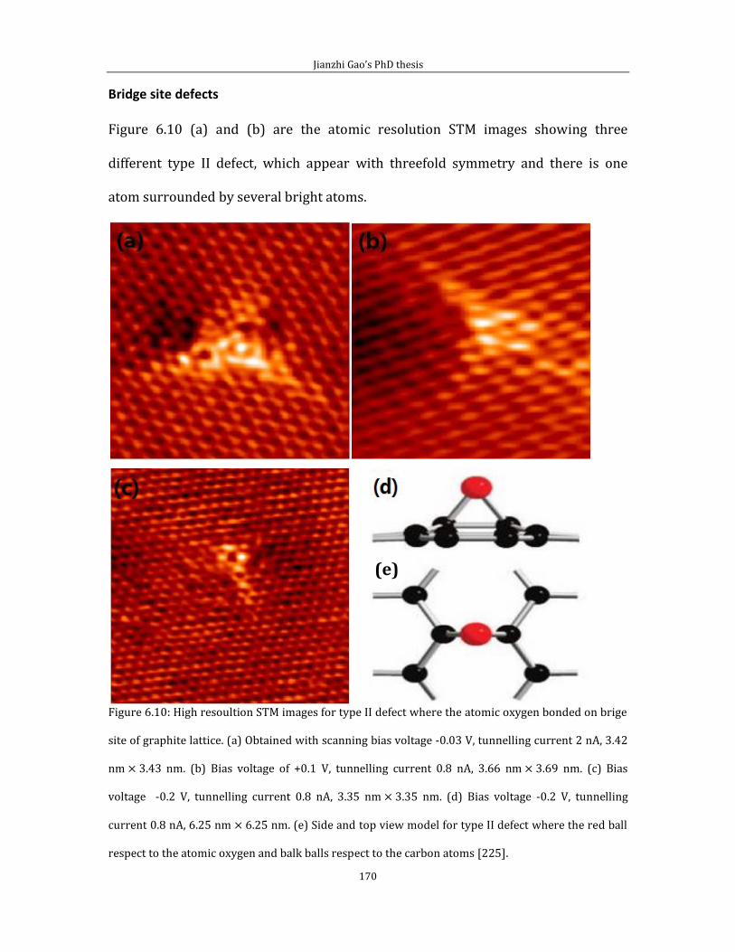
Jianzhi Gao’s PhD thesis
170
Bridge site defects
Figure 6.10 (a) and (b) are the atomic resolution STM images showing three
different type II defect, which appear with threefold symmetry and there is one
atom surrounded by several bright atoms.
Figure 6.10: High resoultion STM images for type II defect where the atomic oxygen bonded on brige
site of graphite lattice. (a) Obtained with scanning bias voltage -0.03 V, tunnelling current 2 nA, 3.42
nm 3.43 nm. (b) Bias voltage of +0.1 V, tunnelling current 0.8 nA, 3.66 nm 3.69 nm. (c) Bias
voltage -0.2 V, tunnelling current 0.8 nA, 3.35 nm 3.35 nm. (d) Bias voltage -0.2 V, tunnelling
current 0.8 nA, 6.25 nm 6.25 nm. (e) Side and top view model for type II defect where the red ball
respect to the atomic oxygen and balk balls respect to the carbon atoms [225].
(e)
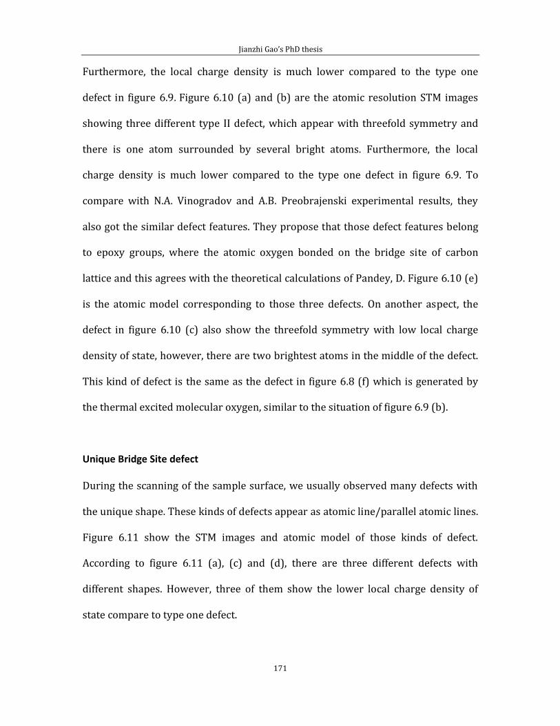
Jianzhi Gao’s PhD thesis
171
Furthermore, the local charge density is much lower compared to the type one
defect in figure 6.9. Figure 6.10 (a) and (b) are the atomic resolution STM images
showing three different type II defect, which appear with threefold symmetry and
there is one atom surrounded by several bright atoms. Furthermore, the local
charge density is much lower compared to the type one defect in figure 6.9. To
compare with N.A. Vinogradov and A.B. Preobrajenski experimental results, they
also got the similar defect features. They propose that those defect features belong
to epoxy groups, where the atomic oxygen bonded on the bridge site of carbon
lattice and this agrees with the theoretical calculations of Pandey, D. Figure 6.10 (e)
is the atomic model corresponding to those three defects. On another aspect, the
defect in figure 6.10 (c) also show the threefold symmetry with low local charge
density of state, however, there are two brightest atoms in the middle of the defect.
This kind of defect is the same as the defect in figure 6.8 (f) which is generated by
the thermal excited molecular oxygen, similar to the situation of figure 6.9 (b).
Unique Bridge Site defect
During the scanning of the sample surface, we usually observed many defects with
the unique shape. These kinds of defects appear as atomic line/parallel atomic lines.
Figure 6.11 show the STM images and atomic model of those kinds of defect.
According to figure 6.11 (a), (c) and (d), there are three different defects with
different shapes. However, three of them show the lower local charge density of
state compare to type one defect.
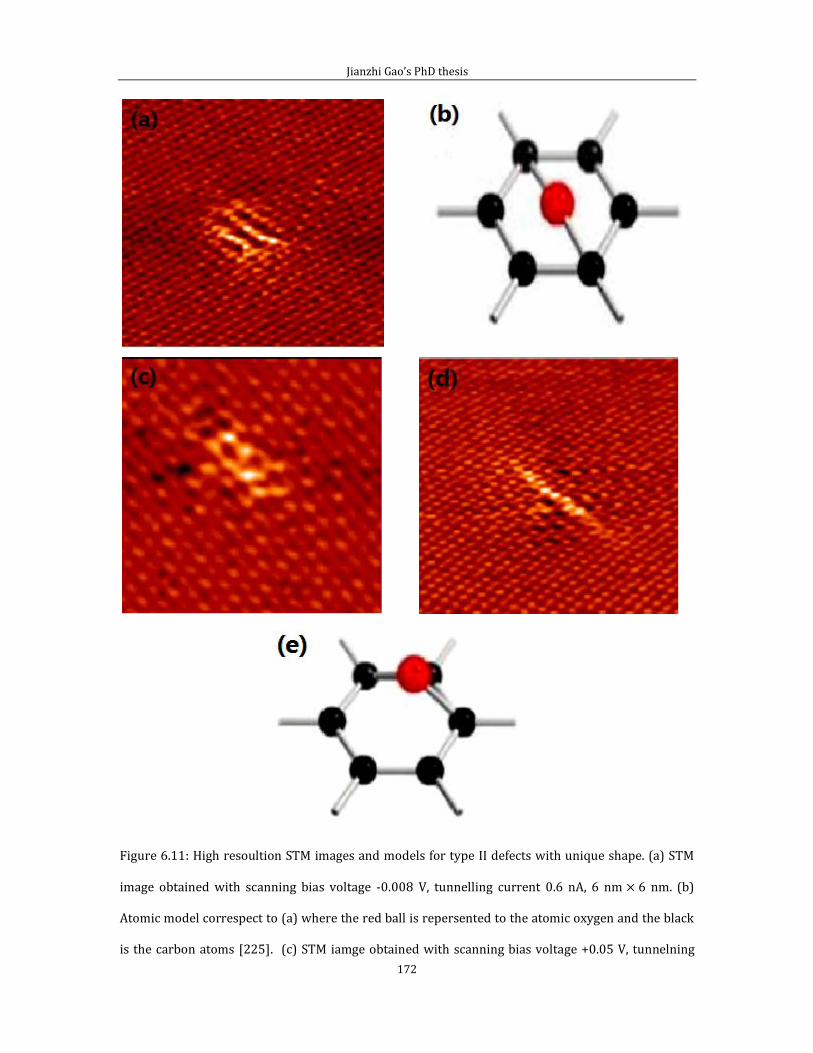
Jianzhi Gao’s PhD thesis
172
Figure 6.11: High resoultion STM images and models for type II defects with unique shape. (a) STM
image obtained with scanning bias voltage -0.008 V, tunnelling current 0.6 nA, 6 nm 6 nm. (b)
Atomic model correspect to (a) where the red ball is repersented to the atomic oxygen and the black
is the carbon atoms [225]. (c) STM iamge obtained with scanning bias voltage +0.05 V, tunnelning

Jianzhi Gao’s PhD thesis
173
current 0.3 nA, 3.22 nm 2.92 nm. (d) Bias voltage -0.008 V, tunnelning current 0.6 nA, 6 nm 6 nm.
(e) Model correspect to (c) and (d) the red ball respect to the atomic oxygen and balk balls respect to
the carbon atoms [225].
From the account above, this type of defect should belong to type II defect.
Therefore, those unique shape defects belong to the bridge situation. Figure 6.11 (b)
is the model for (a), where the red atomic oxygen sits in the middle of the carbon
ring and is bonded with two carbon atoms, hence form the three parallel atomic
lines. However, for the situation in (c) and (d), they are bonded in the same way but
with different site of carbon atoms. From our prediction, defect appeared in (c) and
(d) are bonded as the shown model in (e). Furthermore, this will cause two different
bonding forms. As we know, there are two different site of carbon atoms on the
graphite surface, namely, α and β site. However, the β site carbon atoms appear with
lower local charge density of state than the α site carbon atoms when they are under
scanning of STM. Therefore, when the atomic oxygen bonded with two α site carbon
atoms, they will form the atomic line shape and appear with high local charged
density of state. Compare with the β site carbon atoms at the neighbouring this
atomic line will become more obvious under the STM image and appear as a single
atomic line like (d). However, for another aspect, if the atomic oxygen boned with
two β site carbon atoms, it will form the atomic line shape but with the lower local
charge density of state than the previous one, and the neighbouring α sites carbon
atoms will appear with slightly lower local charge density of state. Hence, there will
be two parallel atomic lines appeared where one line is bright and another line is
less bright, just like the image in (c).
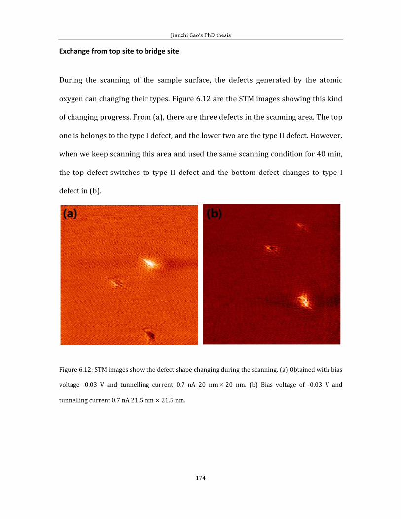
Jianzhi Gao’s PhD thesis
174
Exchange from top site to bridge site
During the scanning of the sample surface, the defects generated by the atomic
oxygen can changing their types. Figure 6.12 are the STM images showing this kind
of changing progress. From (a), there are three defects in the scanning area. The top
one is belongs to the type I defect, and the lower two are the type II defect. However,
when we keep scanning this area and used the same scanning condition for 40 min,
the top defect switches to type II defect and the bottom defect changes to type I
defect in (b).
Figure 6.12: STM images show the defect shape changing during the scanning. (a) Obtained with bias
voltage -0.03 V and tunnelling current 0.7 nA 20 nm 20 nm. (b) Bias voltage of -0.03 V and
tunnelling current 0.7 nA 21.5 nm 21.5 nm.
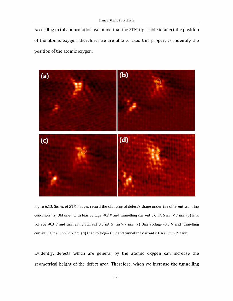
Jianzhi Gao’s PhD thesis
175
According to this information, we found that the STM tip is able to affect the position
of the atomic oxygen, therefore, we are able to used this properties indentify the
position of the atomic oxygen.
Figire 6.13: Series of STM images record the changing of defect’s shape under the different scanning
condition. (a) Obtained with bias voltage -0.3 V and tunnelling current 0.6 nA 5 nm 7 nm. (b) Bias
voltage -0.3 V and tunnelling current 0.8 nA 5 nm 7 nm. (c) Bias voltage -0.3 V and tunnelling
current 0.8 nA 5 nm 7 nm. (d) Bias voltage -0.3 V and tunnelling current 0.8 nA 5 nm 7 nm.
Evidently, defects which are general by the atomic oxygen can increase the
geometrical height of the defect area. Therefore, when we increase the tunnelling
Jianzhi Gao’s PhD thesis
176
current during scanning it can decrease the distance between the sample and the tip.
Finally, the STM tip will be close enough to influence the atomic oxygen. Moreover,
we are able to identify the position of the atomic oxygen by comparing the atomic
resolution STM images of defects before and after the a change in tunnelling current.
Figure 6.13 are the series of STM images recorded in this progress. From (a), we can
see that there is one defect with the shape of parallel atomic lines which shows the
high local charge density. The image is taken under the tunnelling current of 0.6 nA.
We increased the tunnelling current to 0.8 nA in (b). We can see clearly, the atom
inside the yellow circle start to move to the left side and the local charge density
decreases dramatically. But this atom moved back to its original position at (c) and
forms the original defect shape with the similar local charge density in (d). From
those phenomena, we can confirm that the atom seriously affect the local charge
density of state where inside the yellow circle is atomic oxygen.
Contrast properties
According to figure 6.7, we already know that defects generated by atomic oxygen
have bias dependent properties, the contrast of the defects will change with the
different polarity bias. This is in agreement with the nitrogen case. Figure 6.7 are the
STM images showing the contrast changing properties of defects. From (a), we can
see, there are many bright defect features in the scanning area. Where defects with
the higher local charge density of state are the type I defect and defect with the
lower local charge density of state is the type II defect.
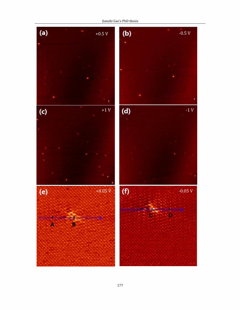
Jianzhi Gao’s PhD thesis
177
+0.5 V -0.5 V
+1 V -1 V
+0.05 V -0.05 V
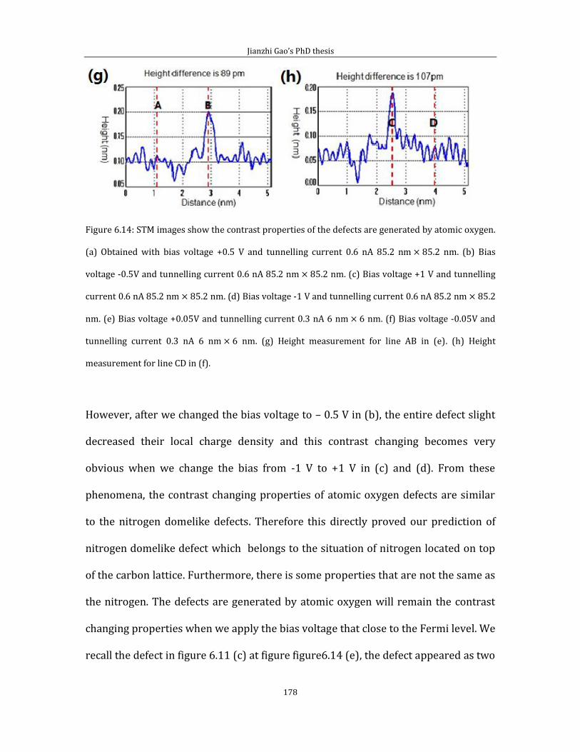
Jianzhi Gao’s PhD thesis
178
Figure 6.14: STM images show the contrast properties of the defects are generated by atomic oxygen.
(a) Obtained with bias voltage +0.5 V and tunnelling current 0.6 nA 85.2 nm 85.2 nm. (b) Bias
voltage -0.5V and tunnelling current 0.6 nA 85.2 nm 85.2 nm. (c) Bias voltage +1 V and tunnelling
current 0.6 nA 85.2 nm 85.2 nm. (d) Bias voltage -1 V and tunnelling current 0.6 nA 85.2 nm 85.2
nm. (e) Bias voltage +0.05V and tunnelling current 0.3 nA 6 nm 6 nm. (f) Bias voltage -0.05V and
tunnelling current 0.3 nA 6 nm 6 nm. (g) Height measurement for line AB in (e). (h) Height
measurement for line CD in (f).
However, after we changed the bias voltage to – 0.5 V in (b), the entire defect slight
decreased their local charge density and this contrast changing becomes very
obvious when we change the bias from -1 V to +1 V in (c) and (d). From these
phenomena, the contrast changing properties of atomic oxygen defects are similar
to the nitrogen domelike defects. Therefore this directly proved our prediction of
nitrogen domelike defect which belongs to the situation of nitrogen located on top
of the carbon lattice. Furthermore, there is some properties that are not the same as
the nitrogen. The defects are generated by atomic oxygen will remain the contrast
changing properties when we apply the bias voltage that close to the Fermi level. We
recall the defect in figure 6.11 (c) at figure figure6.14 (e), the defect appeared as two

Jianzhi Gao’s PhD thesis
179
bright atomic line structure under the scanning bias of +0.05 V. However when we
change to -0.05 V, there are several atoms become less bright in (f), hence we can
conform the oxygen defects will keep the contrast properties even the bias voltage is
close to the Fermi energy level and this did not happen in the nitrogen case.
However, according to the height measurement in (g) and (h), we found that under
the negative bias voltage, defect in (f) has the higher local charge density, and the
defect with the positive bias voltage has the lower charge density. This contrast
changing model is similar to the nitrogen substitutional doped on graphite surface.
We predicted, when the atomic oxygen chemical absorb on graphite surface, the
energy level of atomic oxygen are closed to the Fermi energy level, therefore, it has
enough electron to tunnelling out under the negative bias voltage and electrons
from the tip are hardly tunnel in to the oxygen energy level under the positive bias
voltage. However, the atomic oxygen can attract the electrons from the surround
carbon atoms and make their electron orbit empty as the atomic vacancy, hence the
contrast properties are similar to the nitrogen domelike defect under large bias
scanning.
In summary, from our experimental results, we have successfully fixed the Pt/PtO
clusters using surface defects created by atomic oxygen. Moreover, we identified
two different types of oxygen point defects based on their different local charge
density of states. On another hand, we are able to use the STM to find the positions
of the atomic oxygen, also proved the contrast properties of the oxygen point defect

Jianzhi Gao’s PhD thesis
180
are similar to the nitrogen domelike defects. Both type of defects are created by
external atom/atoms located on top of the HOPG (0001). But, the contrast
properties for the oxygen defects becomes different from the domelike defects when
tunneling occurs from electrons close to the Fermi energy level. Hence, defects
generated by argon, nitrogen and atomic oxygen have different properties, allowing
them to be separately identified. However, the electronic properties and the
structural information of different types of oxygen defect still require further
investigation.
Jianzhi Gao’s PhD thesis
181
Chapter 7 Conclusion
For alkanethiolate self-assembled monolayers on Au (111), we created four
different alkanethiolate self-assembled monolayers on Au (111) namely:
methylthiolate (MT), ethylthiolate (ET), propylthiolate (PT) and methyl-
propylthiolated (M-PT) monolayers. Our experimental data proved that (√3 × √3)-
R300 is absented for MT, ET and PT monolayers. The surface structure of these
consist of AAD units with the (3 × 4) lattice at a surface coverage 0.33 ML. The 3 4
phase of the C3 monolayer is broken into smaller domains by gaps, with saturation
coverage slightly less than 0.33 ML. By considering two different arrangements,
there are two ordered structures. Type 1 structure consists of four rows of AAD
units that are packed between the boundaries with surface coverage equal to 0.328
ML. For type 2 structure, there are two AAD rows between the gaps with surface
coverage 0.325 ML. The formation of the 3 4 phase involves some stress within
the molecular layer. The formation of type 1 and 2 structures observed for PT
monolayers is a result of stress relieve. The stress prevents the formation of a long-
range-ordered 3 4 phase for PT. For alkanethiols with even longer chains (C>3),
the Van der Waals interaction scales with the chain length, so there is a point where
stress is so high that the 3 4 phase transforms into the well known (3 2√3)-rect.
phase and the alkane chains become more regularly spaced. Furthermore, for very
long alkane chains, the spacing between alkane chains is very uniform apart from
the interfacial region and the ends of the alkane chains would appear to have a (√3 ×
√3)R30o structure when looking from above. In addition, there are two different PT
Jianzhi Gao’s PhD thesis
182
striped phases obtained after the thermal annealing process with low coverage; one
of them can be described by a (3 3 x 3)-R30o lattice with surface coverage equal
to 0.22 ML and another striped phase with neighbouring stripes separated by a 5.5 a
distance with a period equal to 11a and the coverage equals to 0.18 ML.
For research conducted on HOPG, the key findings are: 1) Shallow implantation of N
gives rise to several N-C bonded species including substitutional N, interstitial N and
N bonded to C on the top surface. 2) Deposition of atomic oxygen on HOPG leads to
the formation of mainly two types of bonding configurations. One is bridge-bonded
oxygen and the other is atop-bonded oxygen. 3) The chemisorbed atomic oxygen
serves as an anchoring point for PtO clusters. This is a useful way of fixing PtO
particles without damaging the HOPG lattice. Useful work in the future include local
spectroscopic analysis of N and O dopant (STS) and N deposition from an atomic
source.
References
Jianzhi Gao’s PhD thesis
183
[1] J. C. Love, L. A. Estroff, J. K. Kriebel, et al, Chem. Rev., 2005, 105, 1103.
[2] G. Zhi,P. H. Liang,Surface Science and Engineering,Shanghai, 2006.
[3] A. W. Adamson, A .P. Gast, Physical Chemistry of Surfaces, Wiley-Interscience, New York, 1997.
[4] K. S. Novoselov, A. K. Geim, Science, 2004, 306, 666.
[5] G. Ertl, Angewandte Chemie-International Edition, 2008, 47, 3524.
[6] G. Ertl, H. J. Freund, Physics Today, 1999, 52, 32.
[7] B. Franklin, Philos. Trans. R. Soc. London, 1774, 64, 445.
[8] A. Pockels, Nature ,1891, 43, 437.
[9] I. Langmuir, J. Am. Chem. Soc., 1917, 39, 1848.
[10] K. Blodgett, J. Am. Chem. Soc. 1935, 57, 1007.
[11] J. Y. Kim, K. Lee, N. E. Coates, et al, Science, 2007, 317, 222.
[12] C. Vericat, M. E. Vel, G. Benitez, et al, Chem. Soc. Rev., 2010, 39, 1805.
[13] X. Jiang, D. A. Bruzewicz, A. P. Wong, et al, Proc. Natl. Acad. Sci. U. S. A., 2005, 102, 975.
[14] S. Takeuchi, W. R. DiLuzio, D. B. Weibel, et al, Nano Lett., 2005, 5, 1819.
[15] P. L. Schilardi, P. Dip, P. C. Dos Santos Claro, et al, Chem.Eur. J., 2006, 12, 38.
[16] D. Burshtain and D. Mandler, Phys. Chem. Chem. Phys., 2006, 8, 158.
[17] U. Drechsler, B. Erdogan and V. M. Rotello, Chem.Eur. J., 2004, 10, 5570.
[18] M. C. Daniel and D. Astruc, Chem. Rev., 2004, 104, 293.
[19] M. Brust, M. Walker, D. Bethell, et al, J. Chem. Soc., Chem. Commun., 1994, 801.
[20] T. Shimizu, T. Teranishi, S. Hasegawa, et al, J. Phys. Chem. B, 2003, 107, 2719.
[21] R. Maboudian, W. R. Ashurst and C. Carraro, Sens. Actuators A, 2000, 82, 219.
[22] L. A. Bumm, J. J. Arnold, M. T. Cygan, et al, Science, 1996, 271, 1705.
[23] T. Sugawara and M. M. Matsushita, J. Mater. Chem., 2009, 19, 1738.
[24] A. L. Harris, L. Rothberg, L. H. Dubois, et al, Phys. Rev. Lett., 1990, 64, 2086.
[25] R. Heinz and J. P. Rabe, Langmuir, 1995, 11, 506.
[26] A. Nemetz, T. Fischer, A. Ulman, et al, J. Chem. Phys., 1993, 98, 5912.
[27] A. Dhirani, M. A. Hines, A. J. Fisher, et al, Langmuir, 1995, 11, 2609.
[28] P. Fenter, P. Eisenberger, J. Li, N. Camillone, et al, Langmuir, 1991, 7, 2013.
[29] G. D. Aloisi, M. Cavallini, M. Innocenti, et al, J. Phys. Chem. B, 1997, 101, 4774.
[30] M. Yu, S. M. Driver and D. P. Woodruff, Langmuir, 2005, 21, 7285.
[31] H. Rieley, G. K. Kendall, R. G. Jones, et al, Langmuir, 1999, 15, 8856.
[32] M. Fonticelli, O. Azzaroni, G. Benitez, et al, J. Phys. Chem. B, 2004, 108, 1898.
[33] D. Torres, P. Carro, R. C. Salvarezza, et al, Phys. Rev. Lett., 2006, 97, 226103.
[34] F. Schreiber, Prog.Surf. Sci., 2000, 65, 151.
[35] O. Azzaroni, M. E. Vela, M. Fonticelli, et al, J. Phys. Chem. B, 2003, 107, 13446.
[36] A. Imanishi, K. Isawa, F. Matsui, et al, Surf. Sci., 1998, 407, 282.
Jianzhi Gao’s PhD thesis
184
[37] H. Rieley, G. K. Kendall, A. Chan, et al, Surf. Sci., 1997, 392, 143.
[38] J. C. Love, D. B. Wolfe, R. Haasch, et al, J. Am. Chem. Soc., 2003, 125, 2597.
[39] A. Carvalho, M. Geissler, H. Schmid, et al, Langmuir, 2002, 18, 2406.
[40] H. Murayama, N. Ichikuni, Y. Negishi, et al, Chem. Phys. Lett., 2003, 376 ,26.
[41] C. Majumder, Langmuir, 2008, 24, 10838.
[42] J. A. Williams and C. B. Gorman, J. Phys. Chem. C, 2007, 111, 12804.
[43] G. Corthey, A. A. Rubert, G. A. Benitez, et al, J. Phys. Chem.C,2009, 113, 6735.
[44] J. Perdereau, J. P. Biberian, and G. E. Rhead, J. Phys. F: Metal Phys.,1974, 4, 798.
[45] M. A. van hove, R. J. Koestner, et al, Surf. Sci.,1981, 103, 189.
[46] H. Melle, and E. Menzel, Z. Naturforsh. Teil A ,1978, 33, 282.
[47] J. C. Heyraud, and J. J. Metois, Surf. Sci.,1980, 100, 519.
[48] Y. Tanishiro, H. Kanamori, K. Takayanagi, et al, Surf. Sci.,1981, 101, 395.
[49] U. Harten, A. M. Lahee, J. Peter Toennies, and Ch. Woll, Phys. Rev. Lett. 1985, 54, 2619.
[50] F. C. Frank, and J. H. van der Merwe, Proc. R. Soc.,1949,London 198, 205.
[51] Per Bak, Rep. Prog. Phys. 1982, 45, 58.
[52] M. El-Batanouny, S. Burdick, K. M. Martini, and P. Stancioff, Phys. Rev. Lett.,1987, 58, 2762.
[53] S. Narasimhan, and D. Vanderbilt, Phys. Rev. Lett., 1992,69, 1564.
[54] D. D. Chambliss, R. J. Wilson, and S. Chiang, J. Vac. Sci. Technol. B, 1991,9, 933. [55] D. D. Chambliss, R. J. Wilson, and S. Chiang, Phys. Rev. Lett.,1991, 66, 1721. [56] K. G. Huang, D. Gibbs, D. M. Zehner, A. R. Sandy, and S. G. J. Mochrie, Phys. Rev. Lett.,1990, 65, 3313. [57] Ch. Woll, S. Chiang, R. J. Wilson, and P. H. Lippel, Phys. Rev. B,1989, 39, 7988. [58] J. V. Barth, H. Brune, G. Ertl, and R. J. Behm, Phys. Rev. B,1990, 42, 9307.
[59] B. D. Gates, Q. Xu, M. Stewart, et al, Chem. Rev., 2005, 105, 1171.
[60] R. G. Nuzzo and D. L. Allara, J. Am. Chem. Soc., 1983, 105, 4481.
[61] D. L. Allara and R. G. Nuzzo, Langmuir, 1985, 1, 45.
[62] D. P. Woodruff , T. A. Delchar, Modern Techniques of Surface Science, Cambridge University Press, 2 edition, 1994.
[63] D. K Schwartz, Annu. Rev. Phys. Chem., 2001, 52, 107.
[64] H. Kondoh, H. Nozoye, J. Phys. Chem. B, 1999, 103, 2585.
[65] M. Ohara, Y. Kim, M. Kawai, Langmuir, 2005, 21, 4779.
[66] J. Ge Zhou, F. Hagelberg, Phys. Rev. Lett., 2006, 97, 045505.
[67] I. I. Rzeznicka, J. Lee, P. Maksymovych, et al, J. Phys. Chem. B, 2005, 109, 15992.
[68] P. Maksymovych, D. C. Sorescu, and J. T. Yates, J. Phys. Chem. B, 2006, 110, 21161.
[69] P. Maksymovych, D. C. Sorescu, K. D. Jordan, et al, Science, 2008, 322, 1664.
[70] H. Kondoh, C. Kondama, H. Sumida, et al, J. Chem. Phys., 1999, 111, 1175.
Jianzhi Gao’s PhD thesis
185
[71] G. E. Poirier, Langmuir, 1999,15, 1167.
[72] F. Schreiber, A. Eberhardt, T. Y. B. Leung, et al, Phys. Rev. B,1998,57, 12476.
[73] L. M. Rodriguez, J. E. Gayone, E. A. Sanchez, et al, J. Am. Chem. Soc., 2007, 129, 7807.
[74] X. Torrelles, E. Barrena, C. Munuera, et al, Langmuir, 2004, 20, 9396.
[75] Y. Yourdshahyan, A. Rappe, J. Chem. Phys. 2002, 117, 825.
[76] C. E. D. Chidsey, G. Y. Liu, P. Rowntree, et al, J. Chem. Phys., 1989, 91, 4421.
[77] L. Strong, G. M. Whitesides, Langmuir, 1988, 4, 546.
[78] C. E. D. Chidsey, D. N. Loiacono, Langmuir, 1990, 6, 682.
[79] A. I. Kitaigorodskii, Organic Chemistry Crystallography, Consultants Bureau, New York, 1961.
[80] R. G. Nuzzo, E. M. Korenic, L. H. Dubois, J. Chem. Phys., 1990, 93, 767.
[81] R. G. Nuzzo, L. H. Dubois, D. L. Allara, J. Am. Chem. Soc., 1990, 112, 558.
[82] E. Barrena, C. Ocal, M. Salmeron, J. Chem. Phys., 2001, 114, 4210.
[83] S. M. Mendoza, I. Arfaoui, S. Zanarini, et al, Langmuir, 2007, 23, 582.
[84] L. H. Dubois, B. R. Zegarski, R. J. Nuzzo, J. Chem. Phys.,1993, 98, 678.
[85] N. Camillone, C. E. D. Chidsey, G. Y. Liu, et al, J. Chem.Phys., 1991, 94, 8493.
[86] E. Delamarche, B. Michel, H. A. Biebuyck, et al, Adv. Mater. 1996, 8, 719.
[87] A. Riposan, G. Liu, J. Phys. Chem. B, 2006, 110, 23926.
[88] C. Schonenberger, J. Jorritsma, J. A. M. Sondaghuethorst, L.G. J. Fokkink , J. Phys. Chem. 1995, 99, 3259.
[89] M. Kawasaki, T. Sato, T. Tanaka, et al, Langmuir, 2000, 16, 1719.
[90] C. G. Zeng, B. Li, B.Wang, et al, J. Chem. Phys., 2002, 117, 851.
[91] B. Li, C. G. Zeng, Q. X. Li, et al, J. Phys. Chem. B, 2003, 107, 972.
[92] J. Noh, H. S.Kato, M. Kawai, et al, J. Phys. Chem. B, 2006, 110, 2793.
[93] E. Ito, K. Konno, J. Noh, et al, Appl.Surf. Sci. 2005, 244, 584.
[94] C. B. Gorman, Y. He, R. L. Carroll, Langmuir, 2001, 17, 5324.
[95] O. Azzaroni, M. E. Vela, H. Martin, et al, Langmuir, 2001, 17, 6647.
[96] E. J. Calvo, M. S. Rothacher, C. Bonazzola, et al, Langmuir, 2005, 21, 7907.
[97] P. Fenter, P. Eisenberger and K. S. Liang, Phys. Rev. Lett., 1993, 70, 2447.
[98] N. Camillone III, C. E. D. Chidsey, G. Y. Liu, et al, J. Chem. Phys., 1993, 98, 3503.
[99] E. Delamarche, B. Michel, H. Kang, et al, Langmuir, 1994, 10, 4103.
[100] N. Camillone, C.E.D. Chidsey, G.Y. Liu, et al, J. Chem. Phys., 1993, 98, 4234.
[101] P. Fenter, A. Eberhardt and P. Eisenberger, Science, 1994, 266, 1216.
[102] N. Nishida, M. Hara, H. Sasabe, et al J. Appl. Phys., 1996, 35, L799.
[103] A. Chaudhuri, T. J. Lerotholi, D. C. Jackson, et al, Phys. Rev. B, 2009, 79, 195439.
[104] A. Chaudhuri, T. J. Lerotholi, D. C. Jackson, et al, Phys. Rev. Lett., 2009, 102, 126101.
Jianzhi Gao’s PhD thesis
186
[105] F. Terán Arce, M. E. Vela, R. C. Salvarezza, et al, J. Chem. Phys., 1998, 109, 5703.
[106] J. Noh, H. S. Kato, M. Kawai, et al, J. Phys. Chem. B, 2002, 106, 13268.
[107] C. Vericat, G. Andreasen, M. E. Vela, et al, J. Chem. Phys., 2001, 115, 6672.
[108] F. Li, L. Tang, W. Zhou, et al, Phys. Chem. Chem. Phys., 2011, 13, 11958.
[109] M. Kind, C. Wöll, Prog. Surf. Sci., 2009, 84, 230.
[110] M. H. Dishner, J. C. Hemminger, and F. J. Feher, Langmuir, 1997, 13, 2318.
[111] O. Voznyy, J. J. Dubowski, J. T. Yates, et al, J. Am. Chem. Soc., 2009, 131, 12989.
[112] P. Mehring, A. Beimborn, and C. Westphal, Appl.Surf. Sci., 2010, 256, 7265.
[113] D. Cavanna, G. Bracco, V. De Renzi, et al, J. Phys. Condens. Matter, 2007, 19, 305019.
[ ] F. M. Danışman, L. Casalis, G. Bracco, et al, J. Phys. Chem. B, 2002, 106, 11771.
[115] G. Bracco, D. Cavanna, S. Thea, et al, Vacuum, 2008, 82, 1421.
[116] J. Zhang, Q. Chi, and J. Ulstrup,Langmuir, 2006, 22, 6203.
[117] A. Chaudhuri, D. C. Jackson, B. Detlefs, et al, Phys. Chem. Chem. Phys., 2010, 12, 3229.
[118] V. De Renzi, R. Di Felice, D. Marchetto, et al, J. Phys. Chem. B, 2004, 108, 16.
[119] R. Staub, M. Toerker, T. Fritz, et al, Langmuir 1998, 14, 6693.
[120] S. Li, L. Xu, L. Wan, et al, J. Phys. Chem. B, 2006, 110, 1794.
[121] H. Hagenstrom, M. A. Schneeweiss, D. M. Kolb, Langmuir, 1999, 15, 2435.
[122] M. Kawasaki, H. Nagayama, Chem. Lett. 2001, 30, 942.
[123] K. Kobayashi, H. Yamada, T. Horiuchi, et al, Jpn. J. Appl. Phys., 1998, 37(part 1), 6183.
[124] M. Sharma, M. Komiyama, J. R. Engstrom, Langmuir, 2008, 24, 9937.
[125] L. B. Picraux, C. D. Zangmeister, J. D. Batteas, Langmuir, 2006, 22, 174.
[126] N. Camillone, T. Y. B. Leung, P. Schwartz, et al, Langmuir, 1996, 12, 2737.
[127] J. Noh, M. Hara, Langmuir, 2001, 17, 7280.
[128] J. Noh, M. Hara, Langmuir, 2002, 18, 1953.
[129] W. P. Fitts, J. M. White, G. E. Poirier, Langmuir, 2002, 18, 1561.
[130] W. P. Fitts, J. M. White, G. E. Poirier Langmuir, 2002, 18, 2096.
[131] Y. Qian, G. Yang, J. Yu, et al, Langmuir, 2003, 19, 6056.
[132] N. Camillone, P. Eisenberger, T. Y. B. Leung, et al, J. Chem. Phys., 1994, 101, 11031.
[133] S. Li, L. Xu, L. Wan, et al, J. Phys. Chem. B, 2006, 110, 1794.
[134] Y. W. Yang, L. J. Fan, Langmuir, 2002, 18, 1157.
[135] P. Maksymovych,; D. C. Sorescu,; J. T. Yates, Jr., Phys. Rev. Lett., 2006, 97, 146103.
[136] P. Maksymovych, J. T. Yates, J. Am. Chem. Soc., 2008, 130, 7518.
[137] P. Maksymovych, Prog. Surf. Sci., 2010, 85, 206.
[138] D. P. Woodruff, Phys. Chem. Chem. Phys., 2008, 10, 7211.
Jianzhi Gao’s PhD thesis
187
[139] D. C. Jackson, A. Chaudhuri, T. J. Lerotholi, et al, Surf. Sci., 2009, 603, 807.
[140] M. Yu, N. Bovet, C. J. Satterley, et al, Phys. Rev. Lett., 2006, 97, 166102.
[141] A. Chaudhuri, D. C. Jackson, B. Detlefs, et al, Phys. Chem. Chem. Phys., 2010, 12, 3229.
[142] P. Maksymovych,; D. C. Sorescu,; J. T. Yates, Jr. Phys. Rev. Lett., 2006, 97, 146103.
[143] P. Maksymovych, J. T. Yates, J. Am. Chem. Soc. 2008, 130, 7518.
[144] F. Li, W. Zhou, Q. Guo, Phys. Rev. B, 2009, 79, 113412.
[145] F. Li, L. Tang, W. Zhou, et al, J. Am. Chem. Soc., 2010, 132(37), 13059. [146] K. S. Novoselov, A. K. Geim, Science,2004,306, supporting online material the rise of grapheme. [147] R. E. Peierls, Quelques proprieties typiques des corpses solides. Ann. I. H. Poincare,1935, 5, 177. [148] L. D. Landau,. Zur Theorie der phasenumwandlungen II. Phys.Z. Sowjetunion, 1937, 11, 26. [149] L. D. Landau, and E. M. Lifshitz, statistical Physics, Part I, Pergamon Press, Oxford, 1980. [150] N. D.Mermin, Phys. Rev.,1968,176, 250. [151] http://nanoprobes.aist-nt.com/apps/HOPG%20info.htm. [152] Richard Turton, Oxford, The physics of solids page 34 (Oxford University press). [153] http://www.optigraph.fta-berlin.de/basics.html. [154] Chemistry land intro, Hybridization in covalent bonds, <-CHM151 Progress Page, . [155] Cosmos magazine the coming age of diamond, C. Aaron, 2010. [156] D. Tomanek, S. G. Louie, Phys. Rev. B.,1987,35, 14. [157] J. Xhie, K. Sattler, Phys. Rev. B., 1993, 47, 23. [158] Chair Experimental Physics VI STM/AFM images University of Augsburg. [159]Nanotec Cervantes FullMode AFM, W. T. Pong and C. Durkan, J. Phys. D., 2005, 38, R329. [160] W. T. Pong and C. Durkan, J. Phys. D,2005, 38, R329. [161] H. Chang and A. J. Bard, Langmuir, 1991, 7, 1143. [162] J. R. Hahn and H. Kang, Phys. Rev. B., 1999, 60, 8. [163] J. Cervenka and C. F. J. Flipse, Phys. Rev. B., 2009, 79, 195429. [164] P. L. Giunta and S. P. Kelty, J. Chem. Phys., 2001, 114, 1807. [165] W. T. Pong, J. Bendall, and C. Durkan, Surf. Sci.,2007, 601, 498. [166] H .Lipson and A. R. Stokes, Proc. R. Soc. Lond. Ser., 1942, A 181,101. [167] J. C. Charlier, J. P. Michenaud and X. Gonze, Phys. Rev. B., 1992, 46, 4531. [168] S. R. Snyder, W. W. Gerberich, and H. S. White, Phys. Rev. B.,1993,47,16. [169] Z. Y. Rong and P. Kuiper, Phys. Rev. B., 1993, 48, 17427. [170] M. Kuwabara, D. R. Clarke and D. A. Smith, Appl. Phys. Lett., 1990, 56, 2396. [171] C. Y. Liu, H. Chang and A. J. Bard, Langmuir, 1991, 7, 1138. [172] I. Amidror, 1999 The Theory of the Moir e Phenomenon (Dordrecht: Kluwer) [173] J. Cervenka, C. F. J. Flipse, Journal of Physics: Conference Series, 2007, 61, 190.
Jianzhi Gao’s PhD thesis
188
[174] W. Choi, C. Kim and H. Kang, Surf. Sci., 1993, 281, 323. [175] B.An, S. Fukuyama, and K. Yokogawa, J. Appl. Phys.,2002, 92, 5. [176] Soton-type of crystalline defect. [177] M. I. Heggie et al. / Local density functional modelling of the Stone-Wales transformation in fullerenes. [178] Y. Niimi, H. Kambara, T. Matsui, D. Yoshioka, and H. Fukuyama, Phys. Rev. Lett., 2006, 97, 23640. [179] X. M. Ding, X. J. Yang, and X. Wang, Surface Physics and Surface Analysis., 2004, Fudan University Press, Shanghai, p1. [180] A. Damascelli, presentation, from internet. [181] G. Binnig, H. Rohrer, ch. Gerber and E. Weibel, Phys. Rev. Lett., 1982, 49, 57. [182] X. Zhang, A Variable Temperature Scanning Tunneling Microscopy Study Of Organizing C60 Molecules On Nanostructured Gold Surface. (PHD thesis), 2010, 135. [183] H. Amara, S. Latil, V. Meunier, Ph. Lambin, and J. C. Charlier Phys. Rev. B, 2007,76, 115423. [184] J. Hahn and H. Kang, Phys. Rev. B., 1999, 60, 6007. [185] A. A. El-Barbary, R. H. Telling, C. P. Ewels, M. I. Heggie, and P. R. Briddon, Phys. Rev. B.,2003, 68, 144107. [186] I. Gouzman, R. Brener, and A. Hoffman, J. Vac. Sci. Technol., 1999, 0734. [187] D. P. Woodruff, Appl. Surf. Sci., 2007, 254, 76.
[188] H. Gronbeck, H. Hakkinen, R. L. Whetten, J. Phys. Chem. C., 2008, 112, 15940.
[189] Y. Wang, Q. Chi, N. S. Hush, J. R. Reimers, J. D. Zhang, J. Ulstrup, J. Phys. Chem. C, 2011, 115, 10630.
[190] C. R. Henry, Surf. Sci. Rep., 1998, 31, 235. [191] J. Libuda, H. J. Freund, Surf. Sci. Rep., 2005, 57, 157.
[192] C. R. Henry, Prog. Surf. Sci., 2005, 80, 92.
[193] C. T. Campbell, Surf. Sci. Rep., 1997, 27, 1.
[194] M. A. Brown, Y. Fujimori, F. Ringleb, X. Shao, F. Stavale, N. Nilius, M. Freund, H. J. Sterrerand, J. Am. Chem. Soc., 2011, 133, 10668. [195] J. Taing, M.H. Chengand, J. C. Hemminger, ACS Nano, 2011, 5, 6325.
[196] L. K. Ono, B. Yuan, H. Heinrich, B. R. Cuenya, J. Phys. Chem. C., 2010, 114, 22119. [197] S. J. Tauster, S. C. Fung, R .L. Garten, J. Am. Chem. Soc., 1979, 100, 170. [198] S. J. Tauster, Acc. Chem. Res., 1987, 20, 389. [199] D. W. Goodman, Catal. Lett., 2005, 99, 1. [200] M. Bowker, P. Stone, P. Morrall, R. Smith, R. Bennett, N. Perkins, R. Kvon, C. Pang, E. Fourre, M. Hall, J. Catal., 2005, 234, 172. [201] D. R. Mullins, K. Z. Zhang, Surf. Sci., 2002, 513, 163. [202] Q. Guo, R.W. Joyner, Appl. Surf. Sci., 1999, 375, 144. [203] J. Gao, Q. Guo, Applied Surface Science, 2012, 258, 5412. [204] E. Ganz, K. Sattler, J. Clarke, Surf. Sci., 1989, 219, 33. [205] L. J. Lewis, P. Jensen, N. Comb, J. L. Barrat, Phys. Rev. B., 2000, 61, 16084.
Jianzhi Gao’s PhD thesis
189
[206] J. H. Ryu, H. Y. Kim, D. H. Kim, D. H. Seo, H. M. Lee, J. Phys. Chem. C., 2010, 114, 2022. [207] P. Jensen, X. Blasé, P. Ordejon, Surf. Sci., 2004, 564, 173. [208] Q. Guo, P. Fallon, J. Yin, R.E. Palmer, Adv. Mater., 2003, 15, 1084. [209] F. Yin, C. Xirouchaki, Q. Guo, R.E. Palmer, Adv. Mater., 2005, 17, 121. [210] L. Chen, A. Yelon, E. Sacher, J. Phys. Chem. C., 2011, 115, 7896. [211] K. Fauth, M. Hessler, D. Batchelor, G. Schultz, Surf. Sci., 2003, 529, 397. [212] D. Q. Yang, E. Sacher, Surf. Sci., 2002, 516, 43. [213] L. Bardotti, P. Jensen, A. Hoareau, M. Treilleux, B. Cabaud, Phys. Rev. Lett., 1995, 74, 4694. [214] S. J. Carroll, K. Seeger, R. E. Palmer, Appl. Phys. Lett., 1998, 72, 305. [215] S. Gibilisco, M. Di Vece, S. Palomba, G. Faraci, R. E. Palmer, J. Chem. Phys., 2006, 125, 084704. [216] H. H bvel, I. Barke, Prog. Surf. Sci., 2006, 81, 53. [217] S. Watcharinyanon, C. Virojanadara, L. I. Johansson, Surf. Sci., 2011, 605, 1918. [218] Z. H. Zhou, F. Gao, D. W. Goodman, Surf. Sci., 2010, 604, L31. [219] R. Zan, U. Bangert, Q. Ramasse, K. S. Novoselov, Small, 2011, 7, 2868. [220] A. Guerrero-Ruiz, P. Badenes, I. Rodriguez-Ramos, Appl. Catal., 1998, A 173, 313. [221] E. Antolini, J. Mater. Sci., 2003, 38, 2995. [222] Q. Ma, R. A. Rosenberg, Phys. Rev. B., 1999, 60, 2827. [223] S. W. Poon, J. S. Pan, E. S. Tok, Phys. Chem. Chem. Phys., 2006, 8, 3326. [224] L. K. Ono, J. R. Croy, H. Heinrich, B. R. Cuenya, J. Phys. Chem. C., 2011, 115, 16856. [225] K. Mkhoyan, W. Contryman, J. Silcox, A. Stewart, G. Eda, C. Mattevi, S. Miller, and M. Chhowalla, Nano Letter, 2009, 9, 3,1058. [226] C. Olsen, P. A. Rowntree, J. Chem. Phys., 1998, 108, 3750. [227] H. Clarke, J. Chem. Educ., 1977, 54, 230. [228] N. A. Vinogradov, K. Schulte, M. L. Ng, A. Mikkelsen, E. Lundgren, N. Martensson, and A. B. Preobrajenski, J. Phys. Chem. C., 2011, 115, 9568. [229] F. S. Li, L. Tang, J. Z. Gao, W. C. Zhou, and Q. Guo, Langmuir, 2012, 28, 11115.