stimulated raman spectroscopy of analytes evanescently ... · stimulated raman spectroscopy of...
TRANSCRIPT
Stimulated Raman spectroscopy of analytesevanescently probed by a silicon nitridephotonic integrated waveguideHAOLAN ZHAO,1,2 STÉPHANE CLEMMEN,1,2 ALI RAZA,1,2 AND ROEL BAETS1,2,*1Photonics Research Group, INTEC, Ghent University-IMEC, Technologiepark-Zwijnaarde 15, 9052 Ghent, Belgium2Center for Nano- and Biophotonics, Ghent University, Technologiepark-Zwijnaarde 15, 9052 Ghent, Belgium*Corresponding author: [email protected]
Received 18 January 2018; revised 16 February 2018; accepted 18 February 2018; posted 20 February 2018 (Doc. ID 319890);published 15 March 2018
We report, to the best of our knowledge, the first demonstra-tion of stimulated Raman spectroscopy enhanced by ananophotonic integrated circuit. The Raman response oflow-concentration dimethyl sulfoxide is evanescently probedvia centimeter-long wire waveguides. A signal enhancementof close to five orders of magnitude, as compared to the caseof on-chip spontaneous Raman scattering, is demonstrated.This significant enhancement factor allows for the use of con-tinuous-wave lasers with milliwatt-level power and uncooleddetectors and, therefore, sets the basis of future all-on-a-chip Raman spectrometers suitable for both gas and liquiddetection. © 2018 Optical Society of America
OCIS codes: (130.0130) Integrated optics; (290.5910) Scattering,
stimulated Raman; (130.6010) Sensors; (230.7370) Waveguides;
(300.6450) Spectroscopy, Raman.
https://doi.org/10.1364/OL.43.001403
Raman spectroscopy has found wide popularity in biomedical,physical, chemical, and environmental areas due to its capabil-ity of identifying molecular fingerprints [1–4]. However, theintrinsic weakness of the Raman scattering process typicallyrequires state-of-the-art high-power laser excitation anddeep-cooled charge-coupled device camera detection that hin-ders broader lower-cost applications of Raman spectroscopy.
Considerable efforts have been devoted to miniaturize Ramansystems with the aim of drastically reducing the cost and size,while enhancing the signal intensity [5]. Waveguide enhance-ment has been proposed and demonstrated as early as 1972[6]. By tightly confining both the excitation and the analytewithin an optical waveguide, the Raman signal is hugely en-hanced via increased interaction volume. Spontaneous Ramanspectroscopy in hollow core photonic crystal fibers (HCPCFs)has been demonstrated for sub-parts per million level gassensing [7,8]. However, watt-level pump power and liquid-nitrogen-cooled detectors are typically still needed in these dem-onstrations. In addition, the extension to liquid analytes is notstraightforward in the fiber platform [9,10].
Silicon nitride nanophotonics is now a very mature photonicplatform providing integrated lasers [11], spectrometers [12],and high-performance spectral functionalities such as filters[13], arrayed-waveguide gratings [14], and Bragg gratings[15]. As a CMOS-compatible technology, silicon nitride pho-tonic integrated circuits are promising for providing a fullyintegrated Raman sensor in a small footprint and at low cost.The silicon nitride platform not only enables Raman-on-a-chipintegration, but also is suitable for both liquid and gas sensingdue to its high refractive index. Spontaneous Raman scatteringwith evanescent excitations and collections has been demon-strated to detect the bulk liquid of isopropylalcohol [16],monolayers [17], and gas in parts per billion level, thanks toa hypersorbent polymer functionalized waveguide [18].Unfortunately, the waveguide enhancement remains too lowfor avoiding the use of deep-cooled detectors in this spontane-ous Raman scattering modality, which hurdles the demonstra-tion of a fully integrated Raman sensor.
Coherent Raman scattering (CRS) is another widely utilizedphenomenon that is capable of enhancing the Raman signal bymany orders of magnitude. CRS is typically implemented usingtwo lasers—a pump laser and a Stokes laser—the difference fre-quency of which excites molecular vibrations in a resonant way.Both of the CRS implementations, coherent anti-stokes Ramanscattering (CARS), and stimulated Raman scattering (SRS),have been extensively applied in vibrational imaging [1].CARS focuses on the detection of a newly generated light ata blue-shift frequency, while SRS focuses on the detection ofrelative intensity variations of the injected beams. AlthoughCARS has been demonstrated in liquid fill capillaries [19],SRS is preferable for waveguide Raman sensors due to its au-tomatic phase matching, unlike CARS which requires challeng-ing dispersion engineering to fulfill the phase-matchingcondition over a rather wide bandwidth. Besides, in the caseof SRS, unlike spontaneous Raman and CARS, the resultingphotocurrent signal scales with the amplitude of both the origi-nal Stokes field and the scattered field which, by itself, isan enhancement mechanism sometimes called self-heterodyneddetection [1]. Moreover, SRS is capable of reproducing the
Letter Vol. 43, No. 6 / 15 March 2018 / Optics Letters 1403
0146-9592/18/061403-04 Journal © 2018 Optical Society of America
spontaneous Raman spectra with linear dependence on concen-tration. Continuous-wave (CW) SRS has been demonstrated inliquid benzene in 1977 [20] and has recently applied forimaging [21]. The potential of waveguide-enhanced SRS hasalready been demonstrated in HCPCFs [22], where an SRSsignal has been observed from H2 and CO2 with a milliwattlevel of CW excitations. Compared to HCPCFs, althoughthe evanescent Raman detection with rib waveguides suffersfrom a reduced signal due to decreased modal overlap, it makesprobing of liquids dramatically easier, enables convenient inte-gration with microfluidics [23], and opens up new applicationsin probing thin films, or even monolayers. On-chip SRS hasthe potential for on-the-spot detection of 2D materials [24],organic materials [25], and bio-chemical interactions [17].
In this Letter, we report for the first time, to the best ofour knowledge, the use of a nanophotonic waveguide for SRSspectroscopy. As a proof-of-principle demonstration, theRaman response of dimethyl sulfoxide (DMSO) is recordedfrom 500 cm−1 to 900 cm−1 with high spectral resolution.Measurements are further performed on the C-S stretch ofDMSO at 670 cm−1 to investigate the performance of our setupin low concentration. The detection limit is 280 mM for DMSOwith a 600 ms time constant for the lock-in amplifier and anaverage power of 60 mW for both beams. With improvementsin light coupling and waveguide design, the sensitivity is ex-pected to be further improved by 3–4 orders of magnitudes.This Letter paves the way toward a low-cost point-of-careRaman sensor that is expected to find applications in drug pro-duction, health monitoring, and on-site environmental sensing.
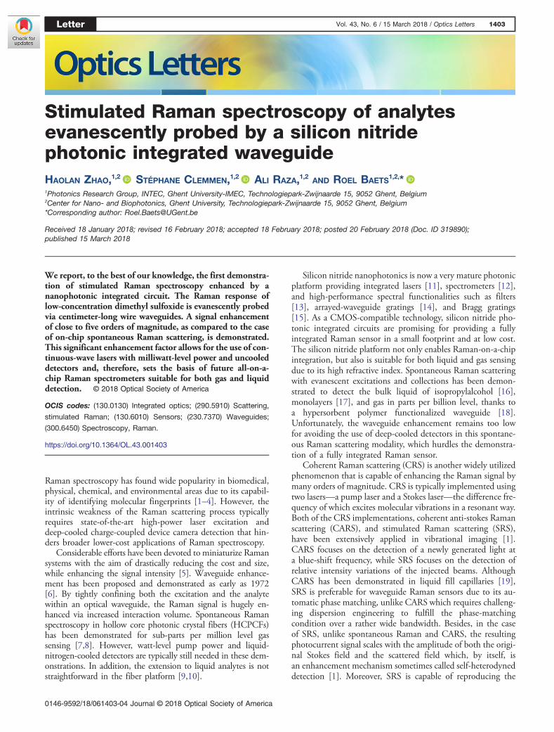
The Raman sensor is made of a nanophotonic waveguide,the geometry of which is chosen as a trade-off between thelow propagation loss and high overlap of the evanescent fieldwith the analyte. The silicon nitride waveguide core is depos-ited through plasma-enhanced chemical vapor deposition(PECVD) and later patterned via deep-UV lithography and re-active ion etching, as depicted in [16]. The 1 cm long wave-guide has a nominal cross section of w × h � 700 × 300 nm,and its width is tapered up to 3 μm at both ends for bettercoupling efficiency. The bottom optical cladding of the wave-guide is a 3.3 μm thick layer of silica, and the top cladding is theanalyte under investigation along the 8 mm sensing area, whilethe remaining 2 mm is cladded by a layer of 1 μm thick silica.A schematic plot of the structure is shown in Figs. 1(a) and1(b). The refractive index of the silicon nitride is 1.9, and
the mode overlap with the analyte varies as a function of therefractive index of the top cladding. Pure DMSO has a refrac-tive index of 1.48, resulting in 14% of the modal power propa-gating inside the analyte, and this power fraction drops to 9.6%for water. To reduce the impact of reflections at the facet of thewaveguide, as discussed later, we terminate the waveguides witha 15 deg angled facet by dicing and polishing of the whole chip.
In the SRS process, the signal appears as a small gain of in-tensity at the Stokes wavelength and is typically read out via thelock-in technique. In our demonstration, the pump is first am-plitude modulated at a certain reference frequency. The modu-lation is then transferred to the Stokes wave via the Ramaninteraction and picked up by a lock-in amplifier. By sweepingthe Stokes wavelength, we can obtain the Raman spectrum ofthe analyte. Figure 1(c) shows the setup of our SRS measure-ment. A laser diode (LD785-SEV300, Thorlabs) emitting at785 nm is used as the pump. It is modulated in intensity witha depth of 30% at 38 MHz through direct current modulation.A CW tunable Ti:sapphire laser (SOLSTIS, M2) is employedas the Stokes beam. Two objectives focus pump and Stokesbeams from opposite sides of the waveguide. Polarizer andhalf-wave plates are used to adjust the injected powers and en-sure that both beams excite the fundamental TE mode of thewaveguide. The transmissions of the beams are monitored foroptical alignment. The input power is 30 mW before the ob-jective for both beams, and the time constant of the lock-inamplifier is set to 100 ms, unless explicitly stated. A small part(4%) of the Stokes beam is tapped before Raman interactionand serves to partially cancel the large DC component in theRaman signal measured by a balanced detector (PDB450A-AC). The electrical signal from the photodiode is then ampli-fied by 104 through a built-in transimpedance amplifier.
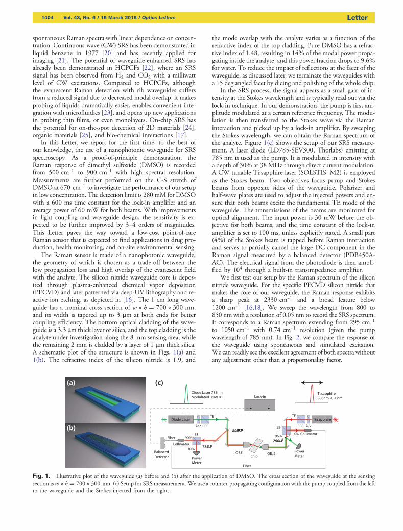
We first test our setup by the Raman spectrum of the siliconnitride waveguide. For the specific PECVD silicon nitride thatmakes the core of our waveguide, the Raman response exhibitsa sharp peak at 2330 cm−1 and a broad feature below1200 cm−1 [16,18]. We sweep the wavelength from 800 to850 nm with a resolution of 0.05 nm to record the SRS spectrum.It corresponds to a Raman spectrum extending from 295 cm−1
to 1050 cm−1 with 0.74 cm−1 resolution (given the pumpwavelength of 785 nm). In Fig. 2, we compare the response ofthe waveguide using spontaneous and stimulated excitation.We can readily see the excellent agreement of both spectra withoutany adjustment other than a proportionality factor.
Fig. 1. Illustrative plot of the waveguide (a) before and (b) after the application of DMSO. The cross section of the waveguide at the sensingsection is w × h � 700 × 300 nm. (c) Setup for SRSmeasurement. We use a counter-propagating configuration with the pump coupled from the leftto the waveguide and the Stokes injected from the right.
1404 Vol. 43, No. 6 / 15 March 2018 / Optics Letters Letter
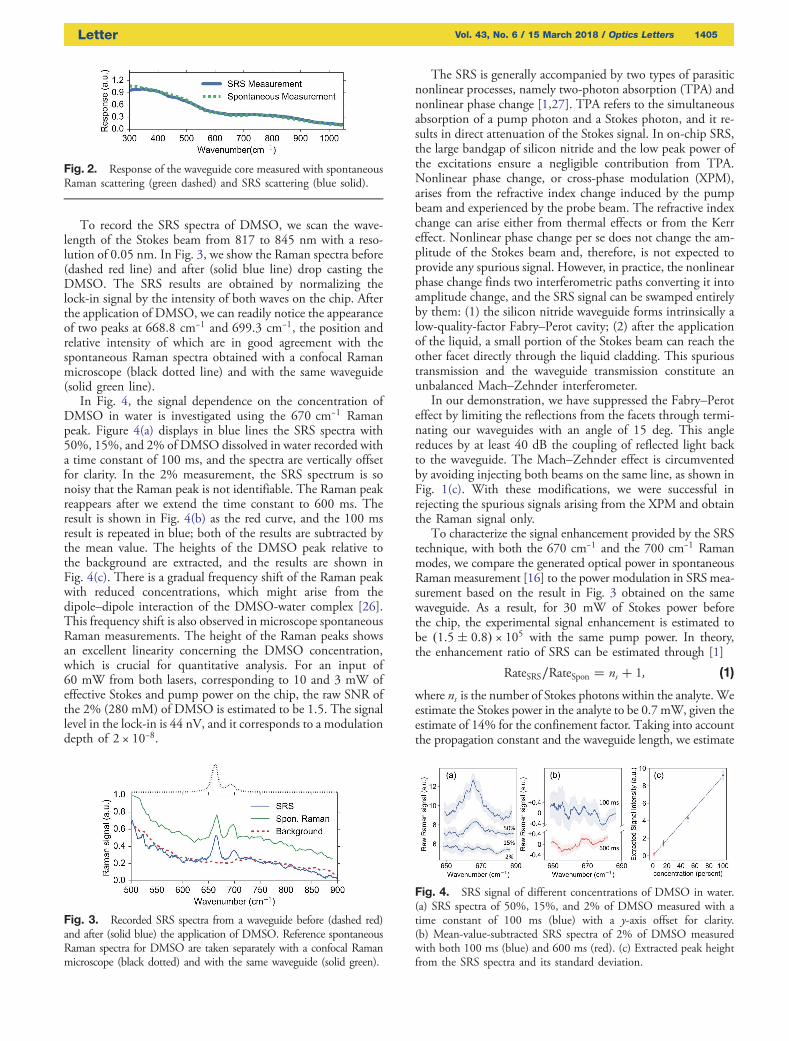
To record the SRS spectra of DMSO, we scan the wave-length of the Stokes beam from 817 to 845 nm with a reso-lution of 0.05 nm. In Fig. 3, we show the Raman spectra before(dashed red line) and after (solid blue line) drop casting theDMSO. The SRS results are obtained by normalizing thelock-in signal by the intensity of both waves on the chip. Afterthe application of DMSO, we can readily notice the appearanceof two peaks at 668.8 cm−1 and 699.3 cm−1, the position andrelative intensity of which are in good agreement with thespontaneous Raman spectra obtained with a confocal Ramanmicroscope (black dotted line) and with the same waveguide(solid green line).
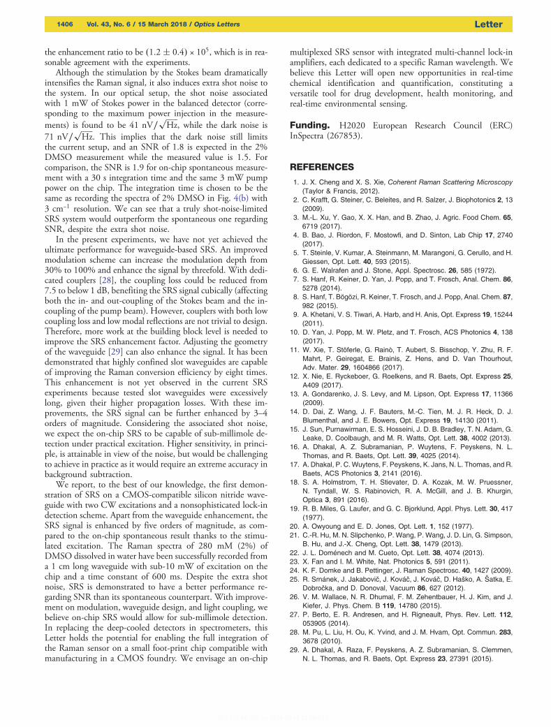
In Fig. 4, the signal dependence on the concentration ofDMSO in water is investigated using the 670 cm−1 Ramanpeak. Figure 4(a) displays in blue lines the SRS spectra with50%, 15%, and 2% of DMSO dissolved in water recorded witha time constant of 100 ms, and the spectra are vertically offsetfor clarity. In the 2% measurement, the SRS spectrum is sonoisy that the Raman peak is not identifiable. The Raman peakreappears after we extend the time constant to 600 ms. Theresult is shown in Fig. 4(b) as the red curve, and the 100 msresult is repeated in blue; both of the results are subtracted bythe mean value. The heights of the DMSO peak relative tothe background are extracted, and the results are shown inFig. 4(c). There is a gradual frequency shift of the Raman peakwith reduced concentrations, which might arise from thedipole–dipole interaction of the DMSO-water complex [26].This frequency shift is also observed in microscope spontaneousRaman measurements. The height of the Raman peaks showsan excellent linearity concerning the DMSO concentration,which is crucial for quantitative analysis. For an input of60 mW from both lasers, corresponding to 10 and 3 mW ofeffective Stokes and pump power on the chip, the raw SNR ofthe 2% (280 mM) of DMSO is estimated to be 1.5. The signallevel in the lock-in is 44 nV, and it corresponds to a modulationdepth of 2 × 10⁻⁸.
The SRS is generally accompanied by two types of parasiticnonlinear processes, namely two-photon absorption (TPA) andnonlinear phase change [1,27]. TPA refers to the simultaneousabsorption of a pump photon and a Stokes photon, and it re-sults in direct attenuation of the Stokes signal. In on-chip SRS,the large bandgap of silicon nitride and the low peak power ofthe excitations ensure a negligible contribution from TPA.Nonlinear phase change, or cross-phase modulation (XPM),arises from the refractive index change induced by the pumpbeam and experienced by the probe beam. The refractive indexchange can arise either from thermal effects or from the Kerreffect. Nonlinear phase change per se does not change the am-plitude of the Stokes beam and, therefore, is not expected toprovide any spurious signal. However, in practice, the nonlinearphase change finds two interferometric paths converting it intoamplitude change, and the SRS signal can be swamped entirelyby them: (1) the silicon nitride waveguide forms intrinsically alow-quality-factor Fabry–Perot cavity; (2) after the applicationof the liquid, a small portion of the Stokes beam can reach theother facet directly through the liquid cladding. This spurioustransmission and the waveguide transmission constitute anunbalanced Mach–Zehnder interferometer.
In our demonstration, we have suppressed the Fabry–Peroteffect by limiting the reflections from the facets through termi-nating our waveguides with an angle of 15 deg. This anglereduces by at least 40 dB the coupling of reflected light backto the waveguide. The Mach–Zehnder effect is circumventedby avoiding injecting both beams on the same line, as shown inFig. 1(c). With these modifications, we were successful inrejecting the spurious signals arising from the XPM and obtainthe Raman signal only.
To characterize the signal enhancement provided by the SRStechnique, with both the 670 cm−1 and the 700 cm−1 Ramanmodes, we compare the generated optical power in spontaneousRaman measurement [16] to the power modulation in SRSmea-surement based on the result in Fig. 3 obtained on the samewaveguide. As a result, for 30 mW of Stokes power beforethe chip, the experimental signal enhancement is estimated tobe �1.5� 0.8� × 105 with the same pump power. In theory,the enhancement ratio of SRS can be estimated through [1]
RateSRS∕RateSpon � ns � 1; (1)
where ns is the number of Stokes photons within the analyte. Weestimate the Stokes power in the analyte to be 0.7 mW, given theestimate of 14% for the confinement factor. Taking into accountthe propagation constant and the waveguide length, we estimate
Fig. 2. Response of the waveguide core measured with spontaneousRaman scattering (green dashed) and SRS scattering (blue solid).
Fig. 3. Recorded SRS spectra from a waveguide before (dashed red)and after (solid blue) the application of DMSO. Reference spontaneousRaman spectra for DMSO are taken separately with a confocal Ramanmicroscope (black dotted) and with the same waveguide (solid green).
Fig. 4. SRS signal of different concentrations of DMSO in water.(a) SRS spectra of 50%, 15%, and 2% of DMSO measured with atime constant of 100 ms (blue) with a y-axis offset for clarity.(b) Mean-value-subtracted SRS spectra of 2% of DMSO measuredwith both 100 ms (blue) and 600 ms (red). (c) Extracted peak heightfrom the SRS spectra and its standard deviation.
Letter Vol. 43, No. 6 / 15 March 2018 / Optics Letters 1405
the enhancement ratio to be �1.2� 0.4� × 105, which is in rea-sonable agreement with the experiments.
Although the stimulation by the Stokes beam dramaticallyintensifies the Raman signal, it also induces extra shot noise tothe system. In our optical setup, the shot noise associatedwith 1 mW of Stokes power in the balanced detector (corre-sponding to the maximum power injection in the measure-ments) is found to be 41 nV∕
ffiffiffiffiffiffi
Hzp
, while the dark noise is71 nV∕
ffiffiffiffiffiffi
Hzp
. This implies that the dark noise still limitsthe current setup, and an SNR of 1.8 is expected in the 2%DMSO measurement while the measured value is 1.5. Forcomparison, the SNR is 1.9 for on-chip spontaneous measure-ment with a 30 s integration time and the same 3 mW pumppower on the chip. The integration time is chosen to be thesame as recording the spectra of 2% DMSO in Fig. 4(b) with3 cm−1 resolution. We can see that a truly shot-noise-limitedSRS system would outperform the spontaneous one regardingSNR, despite the extra shot noise.
In the present experiments, we have not yet achieved theultimate performance for waveguide-based SRS. An improvedmodulation scheme can increase the modulation depth from30% to 100% and enhance the signal by threefold. With dedi-cated couplers [28], the coupling loss could be reduced from7.5 to below 1 dB, benefiting the SRS signal cubically (affectingboth the in- and out-coupling of the Stokes beam and the in-coupling of the pump beam). However, couplers with both lowcoupling loss and low modal reflections are not trivial to design.Therefore, more work at the building block level is needed toimprove the SRS enhancement factor. Adjusting the geometryof the waveguide [29] can also enhance the signal. It has beendemonstrated that highly confined slot waveguides are capableof improving the Raman conversion efficiency by eight times.This enhancement is not yet observed in the current SRSexperiments because tested slot waveguides were excessivelylong, given their higher propagation losses. With these im-provements, the SRS signal can be further enhanced by 3–4orders of magnitude. Considering the associated shot noise,we expect the on-chip SRS to be capable of sub-millimole de-tection under practical excitation. Higher sensitivity, in princi-ple, is attainable in view of the noise, but would be challengingto achieve in practice as it would require an extreme accuracy inbackground subtraction.
We report, to the best of our knowledge, the first demon-stration of SRS on a CMOS-compatible silicon nitride wave-guide with two CW excitations and a nonsophisticated lock-indetection scheme. Apart from the waveguide enhancement, theSRS signal is enhanced by five orders of magnitude, as com-pared to the on-chip spontaneous result thanks to the stimu-lated excitation. The Raman spectra of 280 mM (2%) ofDMSO dissolved in water have been successfully recorded froma 1 cm long waveguide with sub-10 mW of excitation on thechip and a time constant of 600 ms. Despite the extra shotnoise, SRS is demonstrated to have a better performance re-garding SNR than its spontaneous counterpart. With improve-ment on modulation, waveguide design, and light coupling, webelieve on-chip SRS would allow for sub-millimole detection.In replacing the deep-cooled detectors in spectrometers, thisLetter holds the potential for enabling the full integration ofthe Raman sensor on a small foot-print chip compatible withmanufacturing in a CMOS foundry. We envisage an on-chip
multiplexed SRS sensor with integrated multi-channel lock-inamplifiers, each dedicated to a specific Raman wavelength. Webelieve this Letter will open new opportunities in real-timechemical identification and quantification, constituting aversatile tool for drug development, health monitoring, andreal-time environmental sensing.
Funding. H2020 European Research Council (ERC)InSpectra (267853).
REFERENCES
1. J. X. Cheng and X. S. Xie, Coherent Raman Scattering Microscopy(Taylor & Francis, 2012).
2. C. Krafft, G. Steiner, C. Beleites, and R. Salzer, J. Biophotonics 2, 13(2009).
3. M.-L. Xu, Y. Gao, X. X. Han, and B. Zhao, J. Agric. Food Chem. 65,6719 (2017).
4. B. Bao, J. Riordon, F. Mostowfi, and D. Sinton, Lab Chip 17, 2740(2017).
5. T. Steinle, V. Kumar, A. Steinmann, M. Marangoni, G. Cerullo, and H.Giessen, Opt. Lett. 40, 593 (2015).
6. G. E. Walrafen and J. Stone, Appl. Spectrosc. 26, 585 (1972).7. S. Hanf, R. Keiner, D. Yan, J. Popp, and T. Frosch, Anal. Chem. 86,
5278 (2014).8. S. Hanf, T. Bögözi, R. Keiner, T. Frosch, and J. Popp, Anal. Chem. 87,
982 (2015).9. A. Khetani, V. S. Tiwari, A. Harb, and H. Anis, Opt. Express 19, 15244
(2011).10. D. Yan, J. Popp, M. W. Pletz, and T. Frosch, ACS Photonics 4, 138
(2017).11. W. Xie, T. Stöferle, G. Rainò, T. Aubert, S. Bisschop, Y. Zhu, R. F.
Mahrt, P. Geiregat, E. Brainis, Z. Hens, and D. Van Thourhout,Adv. Mater. 29, 1604866 (2017).
12. X. Nie, E. Ryckeboer, G. Roelkens, and R. Baets, Opt. Express 25,A409 (2017).
13. A. Gondarenko, J. S. Levy, and M. Lipson, Opt. Express 17, 11366(2009).
14. D. Dai, Z. Wang, J. F. Bauters, M.-C. Tien, M. J. R. Heck, D. J.Blumenthal, and J. E. Bowers, Opt. Express 19, 14130 (2011).
15. J. Sun, Purnawirman, E. S. Hosseini, J. D. B. Bradley, T. N. Adam, G.Leake, D. Coolbaugh, and M. R. Watts, Opt. Lett. 38, 4002 (2013).
16. A. Dhakal, A. Z. Subramanian, P. Wuytens, F. Peyskens, N. L.Thomas, and R. Baets, Opt. Lett. 39, 4025 (2014).
17. A. Dhakal, P. C. Wuytens, F. Peyskens, K. Jans, N. L. Thomas, and R.Baets, ACS Photonics 3, 2141 (2016).
18. S. A. Holmstrom, T. H. Stievater, D. A. Kozak, M. W. Pruessner,N. Tyndall, W. S. Rabinovich, R. A. McGill, and J. B. Khurgin,Optica 3, 891 (2016).
19. R. B. Miles, G. Laufer, and G. C. Bjorklund, Appl. Phys. Lett. 30, 417(1977).
20. A. Owyoung and E. D. Jones, Opt. Lett. 1, 152 (1977).21. C.-R. Hu, M. N. Slipchenko, P. Wang, P. Wang, J. D. Lin, G. Simpson,
B. Hu, and J.-X. Cheng, Opt. Lett. 38, 1479 (2013).22. J. L. Doménech and M. Cueto, Opt. Lett. 38, 4074 (2013).23. X. Fan and I. M. White, Nat. Photonics 5, 591 (2011).24. K. F. Domke and B. Pettinger, J. Raman Spectrosc. 40, 1427 (2009).25. R. Srnánek, J. Jakabovič, J. Kováč, J. Kováč, D. Haško, A. Šatka, E.
Dobročka, and D. Donoval, Vacuum 86, 627 (2012).26. V. M. Wallace, N. R. Dhumal, F. M. Zehentbauer, H. J. Kim, and J.
Kiefer, J. Phys. Chem. B 119, 14780 (2015).27. P. Berto, E. R. Andresen, and H. Rigneault, Phys. Rev. Lett. 112,
053905 (2014).28. M. Pu, L. Liu, H. Ou, K. Yvind, and J. M. Hvam, Opt. Commun. 283,
3678 (2010).29. A. Dhakal, A. Raza, F. Peyskens, A. Z. Subramanian, S. Clemmen,
N. L. Thomas, and R. Baets, Opt. Express 23, 27391 (2015).
1406 Vol. 43, No. 6 / 15 March 2018 / Optics Letters Letter