stealth dicing dfl - disco corporation · a new ‘‘kiru’’ technology, stealth dicing...
TRANSCRIPT

Laser Application
ABLATION PROCESS
STEALTH DICING
DFL
DFLDFL
DFLDAL
DFLDFL

Modified layer
Short pulse laser
Focusing lens
Workpiece
Application example
DISCO’s laser application lineup supports miniaturized next generation devices Providing the optimum ‘‘Kiru’’ technology for various materials “Kiru” means “Cutting” in Japanese.
• Little or no heat damage of the workpiece
• Non-contact processing with low impact and load
• Ideal for hard workpieces that are very diffi cult to process
• Able to process fi ne streets less than 10 µm in width (depends on workpiece conditions)
It is a processing method that irradiates a workpiece with a very strong laser for a short time to vaporize it.
What is ablation processing ?
Low-k grooving• Inhibits delamination (fi lm peeling)
SEM x200Feed speed: 600mm/s ϖ cut
SEM x2000
• Increases the number of die per wafer by street reduction• Improves feed speed (compared to blade dicing)
Laser full cut
[ Silicon wafer full cut ]
SEM x100
100 µm
SEM x400Feed speed: 500 mm/s 3pass Wafer thickness: 50 µm
• High quality cutting of DAF (Die Attach Film)
Si + DAF full cut
ABLATION PROCESS
Sapphire grooving• Realizes stable processing while restraining sapphire brightness deterioration• Improves CoO with a shape recognition function for broken wafers, and
with multiple-mounted wafer processing
x100Feed speed: 150 mm/s Wafer thickness: 90 µm
[ After breaking Top view image ]
100 µm100 µm
SEM x500Wafer thickness: 80 µm
SEM x750Wafer thickness: 30 µm DAF thickness: 10 µm
[ After breaking SEM image ]
Manual laser saw for 6-inch wafers
DAL7020For 6-inch wafersFor sapphire processing
DFL7020Fully automatic laser saw for 300 mm wafers
DFL7161Fully automatic laser saw for 300 mm wafers
DFL7160Two-head fully automatic laser sawfor 300 mm wafers
DFL7260

Modified layer
Silicon wafer
SEM x500Feed speed: 300 mm/s 1pass Wafer thickness: 100 µm
[ Cross-section photograph ]
GaAs
A new ‘‘Kiru’’ technology, Stealth DicingProviding high quality, high speed wafer processing of MEMS devices and thin wafers
Modified layer
Application example
MEMS[ MEMS die ] [ Edge enlargement ]
1000 µm 100 µm
Fully automatic laser saw for stealth dicing of 300 mm wafers
Fully automatic laser saw for stealth dicing of 200 mm wafers
Inline systemAn inline system can be configured to support the stable processing and handling of ultrathin wafers from wafer thinning to stealth dicing and frame mounting.
Short pulse laser
Focusing lens
• Able to control processing waste because it modifi es the internal part of the workpiece. This is suitable for workpieces that are vulnerable to contamination.
• It is a dry process that does not require cleaning, therefore it is suitable to processes (such as MEMS) that are vulnerable to loading.
• Greatly contributes to street reduction because the kerf width can be made extremely thin.
It is a dicing method that forms a modifi ed layer in the workpiece by focusing a laser inside the workpiece, and then separates the die using a tape expander
What is stealth dicing ?
The DFL7340 and DFL7360 laser saws incorporate
an SD engine, which has a modularized laser and
dedicated optical system. The SD engine has been
developed for DISCO by HAMAMATSU Photonics K.K..
Workpiece
Glass
SEM x50 700 µmt
LiTaO3
SEM x100 350 µmt
[ Cross-section photograph ] [ Cross-section photograph ]
STEALTH DICING
DFL7340 DFM2800DFL7360
DGP8761DFL7360
x100Wafer thickness: 100 µm
[ Cross-section photograph ] [ Top view photograph ]
Sapphire
SEM x200Wafer thickness: 90 µm
SEM x500Wafer thickness: 100 µm
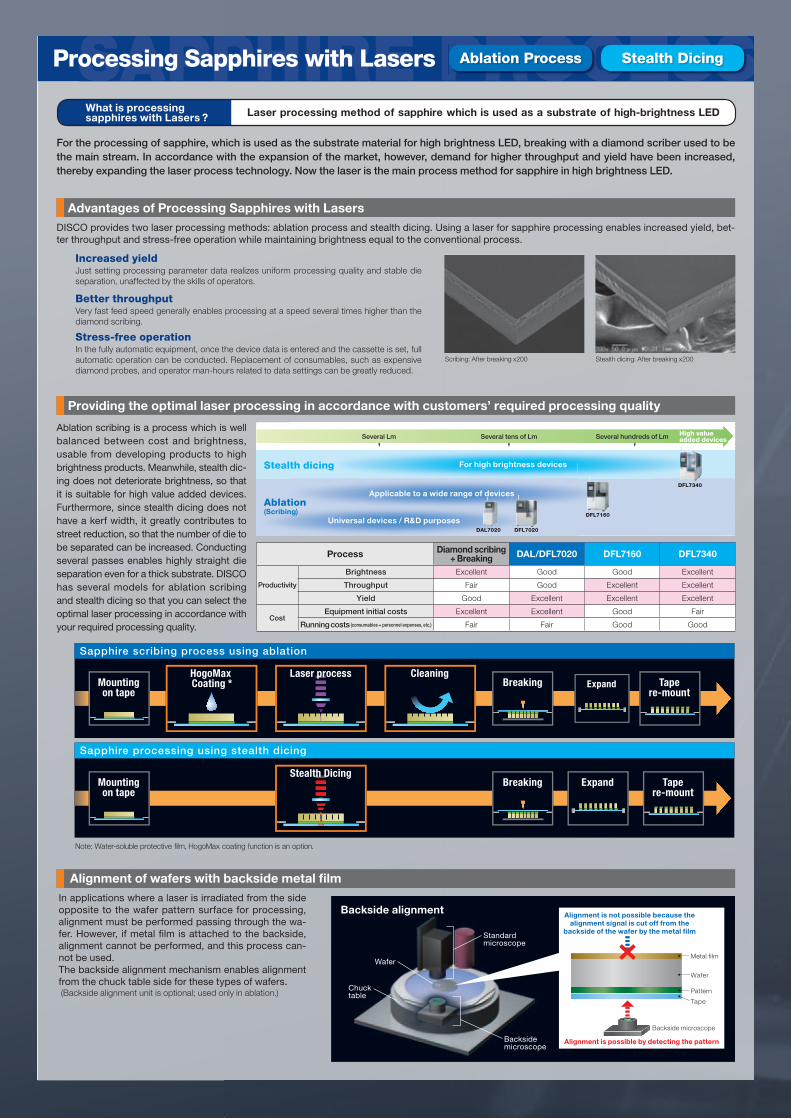
SAPPHIRE PROCESSLaser processing method of sapphire which is used as a substrate of high-brightness LED
Processing Sapphires with Lasers
What is processing sapphires with Lasers ?
Note: Water-soluble protective fi lm, HogoMax coating function is an option.
Alignment of wafers with backside metal fi lmIn applications where a laser is irradiated from the side opposite to the wafer pattern surface for processing, alignment must be performed passing through the wa-fer. However, if metal fi lm is attached to the backside, alignment cannot be performed, and this process can-not be used.The backside alignment mechanism enables alignment from the chuck table side for these types of wafers.(Backsidealignmentunitisoptional;usedonlyinablation.)
Standard microscope
Backside alignment
Wafer
Backside microscope
Backside microscope
Metal film
Alignment is possible by detecting the pattern
Wafer
Pattern
Tape
Chuck table
Alignment is not possible because the alignment signal is cut off from the
backside of the wafer by the metal film
Mounting on tape
Stealth Dicing Breaking Expand Tape re-mount
改質層
Sapphire scribing process using ablation
Sapphire processing using stealth dicing
Mountingon tape
HogoMax Coating *
CleaningBreaking Expand Tape
re-mount
Laser process
Mountingon tape
Breaking Expand Tapere-mount
Stealth Dicing
Advantages of Processing Sapphires with LasersDISCO provides two laser processing methods: ablation process and stealth dicing. Using a laser for sapphire processing enables increased yield, bet-ter throughput and stress-free operation while maintaining brightness equal to the conventional process.
Providing the optimal laser processing in accordance with customers’ required processing quality
Increased yield Just setting processing parameter data realizes uniform processing quality and stable die separation, unaffected by the skills of operators.
Better throughputVery fast feed speed generally enables processing at a speed several times higher than the diamond scribing.
Stress-free operationInthefullyautomaticequipment,oncethedevicedataisenteredandthecassetteisset,fullautomatic operation can be conducted. Replacement of consumables, such as expensive diamond probes, and operator man-hours related to data settings can be greatly reduced.
For the processing of sapphire, which is used as the substrate material for high brightness LED, breaking with a diamond scriber used to be the main stream. In accordance with the expansion of the market, however, demand for higher throughput and yield have been increased, thereby expanding the laser process technology. Now the laser is the main process method for sapphire in high brightness LED.
Scribing:Afterbreakingx200 Stealthdicing:Afterbreakingx200
SAPPHIRE PROCESSAblation ProcessSAPPHIRE PROCESSStealth Dicing
Process Diamond scribing + Breaking DAL/DFL7020 DFL7160 DFL7340
Productivity
Brightness Excellent Good Good Excellent
Throughput Fair Good Excellent Excellent
Yield Good Excellent Excellent Excellent
CostEquipment initial costs Excellent Excellent Good Fair
Running costs (consumables + personnel expenses, etc.) Fair Fair Good Good
Ablation scribing is a process which is well balanced between cost and brightness, usable from developing products to high brightness products. Meanwhile, stealth dic-ing does not deteriorate brightness, so that it is suitable for high value added devices. Furthermore, since stealth dicing does not have a kerf width, it greatly contributes to street reduction, so that the number of die to be separated can be increased. Conducting several passes enables highly straight die separation even for a thick substrate. DISCO has several models for ablation scribing and stealth dicing so that you can select the optimal laser processing in accordance with your required processing quality.
Stealth dicing
Ablation(Scribing)
For high brightness devices
Applicable to a wide range of devices
Universal devices / R&D purposes
High value added devicesSeveral hundreds of Lm
DFL7340
DFL7160
DFL7020DAL7020
Several tens of LmSeveral Lm

LASER FULL CUT
LASER GROOVING
Laser full cut
Laser grooving
Thin silicon wafer full cutThisprocessrealizeshighquality,high-speed full cutting with a laser of thin silicon wafers that are very diffi cut to process.
Laser full cut is effective for thin silicon, compound semiconduc-tors, wafers with backside metal film, high-brightness LED sub-strate, and metals (Cu, molybdenum), and normally cuts into the tape by irradiating a laser for one to several passes on the pat-terned surface. This method realizes high-speed and high-quality processing and great street reduction by focusing the laser beam to a spot less than 10 µm. This laser process also enables Si + DAF (die attach fi lm) full cut.
It is a method that completely cuts the workpiece only with a laser process.What is laser full cut ?
Aluminum nitrideSEMx100150mm/s1pass200µmt
Street Width
TEG
Work
Tape
Backsidemetal film
Laser
x100200mm/s1pass50µmt SEMx300140mm/s1pass100µmt SEMx750Waferthickness:30µmDAFthickness:10µm
Cu full cut x100
LASER FULL CUT
LASER GROOVING
Ablation Process
Ablation Process
Alumina ceramics SEMx100 635µmt
Compound device full cut When processing compound semiconductors, such as GaAs and SiC, high productivity could not be achieved since it was diffi cult to increase the feed speed in the existing blade dicing.Thenon-contactandlow-loadlaserprocess enables high-speed and high-quality processing.
[ GaAs ]
Si + DAF full cutUncut DAF (whiskers) tends to occur when dicingDAFwithablade. It ispossibletosignifi cantly reduce this with a laser cut.
[Cu]
Scribing on hard-to-cut materials + breaking
The materials below, which are diffi cult to cut with a blade, can now be made into die by laser scribing followed by breaking.
• Aluminum nitride used in heat sink materials• Gallium nitride used in laser diode materials• Alumina ceramics, SiC, etc.
It is a process method that forms a narrow groove in the cut street using a laser.
Low-k fi lm and metal layer groovingDelamination (fi lm peeling) can be a problem with blade dicing of wafers with low-k fi lm. Laser grooving, which has no mechanical load, can be used to realize high-quality processing with minimal delamination, thereby con-tributing to higher productivity. DISCO laser grooving is also used in applications where the metal layer (TEG, wiring, circuits, etc.) along the dicing street is removed.
What is laser grooving ?
Laser grooving is a process that is suitable for wafers with low-k fi lm (low dielectric constant). Low-k has been commonly used since the start of 90 nm manufacturing for the miniaturization of semiconductor devices. After forming a narrow groove with the laser in these dif-fi cult to cut materials, the die are separated using blade or laser dicing.
After completely removing a Low-k film and metal wiring on the street by laser grooving, a full cut is conductedinthedicingprocess.DISCOoffersvariousgrooving methods in accordance with the layout of Low-k fi lm and metal wiring as well as the street width.
Low-k grooving example
Street width Blade
Silicon
Metal wiringLaser
Low-k layers
Tape
Silicon
Tape
Full cut with blade or laserComplete removal of the low-k layers and metal on the street with laser
irradiation
Metal full cutThe laserenableshigh-qualityandhigh-speed full cut of metals, such as Cu and molybdenum, used in high-brightness LEDsubstrateandheatsink.Kerflosscanalso be reduced.
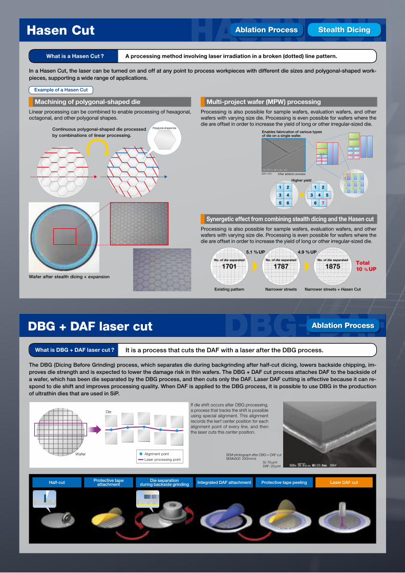
DBG+DAF
HASEN CUT
DBG + DAF laser cut
It is a process that cuts the DAF with a laser after the DBG process.
The DBG (Dicing Before Grinding) process, which separates die during backgrinding after half-cut dicing, lowers backside chipping, im-proves die strength and is expected to lower the damage risk in thin wafers. The DBG + DAF cut process attaches DAF to the backside of a wafer, which has been die separated by the DBG process, and then cuts only the DAF. Laser DAF cutting is effective because it can re-spond to die shift and improves processing quality. When DAF is applied to the DBG process, it is possible to use DBG in the production of ultrathin dies that are used in SiP.
What is DBG + DAF laser cut ?
If die shift occurs after DBG processing, a process that tracks the shift is possible using special alignment. This alignment records the kerf center position for each alignment point of every line, and then the laser cuts this center position.
Die
Wafer Alignment point
Laser processing pointSEM photograph after DBG + DAF cutSEMx500 200mm/s Si: 70 µmt DAF: 20 µmt
Half-cut Protective tape attachment
Die separation during backside grinding Integrated DAF attachment Protective tape peeling Laser DAF cut
Ablation Process
Hasen Cut
In a Hasen Cut, the laser can be turned on and off at any point to process workpieces with different die sizes and polygonal-shaped work-pieces, supporting a wide range of applications.
A processing method involving laser irradiation in a broken (dotted) line pattern.What is a Hasen Cut ?
Example of a Hasen Cut
Polygonal-shaped die
1 2
3 4
5 6
1
After ablation process
2
3 4 5
6 7
Higher yield
SEM ×200
Enables fabrication of various types of die on a single wafer.
Continuous polygonal-shaped die processed by combinations of linear processing.
Ablation Process Stealth Dicing
Machining of polygonal-shaped dieLinear processing can be combined to enable processing of hexagonal, octagonal, and other polygonal shapes.
Multi-project wafer (MPW) processingProcessing is also possible for sample wafers, evaluation wafers, and other wafers with varying size die. Processing is even possible for wafers where the die are offset in order to increase the yield of long or other irregular-sized die.
Synergetic effect from combining stealth dicing and the Hasen cut Processing is also possible for sample wafers, evaluation wafers, and other wafers with varying size die. Processing is even possible for wafers where the die are offset in order to increase the yield of long or other irregular-sized die.
Wafer after stealth dicing + expansion
No. of die separated
1701
5.1 % UP 4.9 % UP
Total10 % UP
No. of die separated
1787No. of die separated
Existing pattern Narrower streets Narrower streets + Hasen Cut
1875
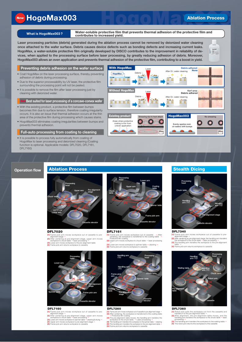
HogoMax003Water-soluble protective fi lm that prevents thermal adhesion of the protective fi lm and contributes to increased yield.
Preventing debris adhesion on the wafer surface•CoatHogoMaxonthelaserprocessingsurface,therebypreventing
adhesion of debris during processing.
•DuetothesuperiorprocessabilitybyUVlaser,theprotectivefilmsurrounding the processing point will not be peeled.
•Itispossibletoremovethefilmafterlaserprocessingjustbycleaning with deionized water.
Best suited for laser processing of a concave-convex wafer•Withtheexistingproduct,aprotectivefilmbetweenbumps
becomes thin due to surface tension, therefore coating irregularity occurs.Itisalsoanissuethatthermaladhesionoccursatthethinarea of the protective fi lm during processing which causes stains.
•HogoMax003eliminatescoatingirregularitiesbetweenbumpsandprevents thermal adhesion.
Full-auto processing from coating to cleaning•ItispossibletoprocessfullyautomaticallyfromcoatingofHogoMaxtolaserprocessinganddeionizedcleaning(Coatingfunctionisoptional.Applicablemodels:DFL7020,DFL7161,DFL7160)
What is HogoMax003 ?
Laser processing particles (debris) generated during the ablation process cannot be removed by deionized water cleaning once attached to the wafer surface. Debris causes device defects such as bonding defects and increasing current leaks. HogoMax, a water-soluble protective fi lm originally developed by DISCO contributes to the improvement in reliability of de-vices, when applied to the processing surface before laser processing, by greatly reducing adhesion of debris. Moreover, HogoMax003 allows an even application and prevents thermal adhesion of the protective fi lm, contributing to a boost in yield.
Best suited for laser processing of a concave-convex waferNew
Si Si Si
Debris
Laser
Laser
After D.I. water cleaning
After D.I. water cleaning
HogoMax
Si Si Si
Debris
Areas where protective coating is thin from uneven application
Evenly applies even on wafers with bumps
No smearingSmearing due to heat attach HogoMax003
With HogoMax
Without HogoMax
Existing product
Debris adhered:None
Kerf area:Debris adhered
HogoMax003Ablation Process
Operation fl ow
DFL7020[1] Frame pick arm moves workpiece out of cassette to pre-
alignment stage →[2] After centering at pre-alignment stage, upper arm moves
workpiece to chuck table → laser processing →[3] Lower arm moves workpiece to the pre-alignment table[4] Frame pick arm returns workpiece to cassette
ロアアーム
Chuck table
Pre-alignment stage
Cassette elevator
Upper arm
Processing head
Lower arm
[1][4]
[2]
[3]
DFL7160[1] Frame pick arm moves workpiece out of cassette to pre-
alignment stage →[2] After centering at pre-alignment stage, upper arm moves
workpiece to chuck table → laser processing →[3] Lower arm moves workpiece to spinner table → cleaning & drying →[4] Upper arm moves workpiece to pre-alignment stage →[5] Frame pick arm returns workpiece to cassette
Chuck table
Pre-alignment stage
Spinner table
Cassette elevator
Upper arm
Processing head
Lower arm
Frame pick arm
[1]
[4]
[2][3]
[5]
DFL7161[1] Frame pick arm moves workpiece out of cassette → After
centering, the workpiece is transferred to the coating table → Protective fi lm coating
[2] Upper arm moves workpiece to chuck table → laser processing →
[3] Lower arm moves workpiece to spinner table → cleaning →[4] Frame pick arm returns workpiece to cassette
Spinner table
Cassette elevator
Upper arm
Processing head Lower arm
Frame pick arm
[1]
[4]
[2]
[3]
Coating table
Chuck table
DFL7260[1] Frame pick arm moves workpiece out of cassette to pre-alignment stage →[2] After centering, the workpiece is transferred to the coating table → Protective fi lm coating
[3] The pre-alignment table moves, the handling arm transfers the workpiece to the chuck table. → Laser processing →
[4] The handling arm transfers the workpiece to the spinner table → cleaning[5] The handling arm transfers the workpiece to the pre-alignment table →[6] Frame pick arm returns workpiece to cassette
Cassette elevator
Frame pick arm
Coating table
Spinner table
Handling arm (T1)
Chuck table
Processing head
Pre-alignment stage
Handling arm (T2)
[1][2]
[3]
[4]
[5]
[6]
DFL7340[1] Frame pick arm moves workpiece out of cassette to pre-
alignment stage →[2] After centering at pre-alignment stage, the handling arm transfers
the workpiece to the chuck table → laser processing →[3] The handling arm transfers the workpiece to the pre-alignment
table →[4] Frame pick arm returns workpiece to cassette
Cassette elevator
Pre-alignment stage
Handling arm (T1) Handling
arm (T2)
Chuck table
Processing head
[1]
[2]
[3]
[4]
DFL7360[1] Robot pick pulls the workpiece out from the cassette and
transfers it to the pre-alignment table →[2] After alignment, the pre-alignment table moves, and the
handling arm transfers the workpiece to the chuck table → laser processing →
[3] The handling arm transfers the workpiece to the waiting table →[4] The robot pick returns the workpiece to the cassette
cassette
Robot pick
Pre-alignment table
Chuck table
Processing head
Handling arm (T1)
Handling arm (T2)
Waiting table
[1]
[2]
[3]
[4]
Ablation Process Stealth Dicing
HogoMax003New

13-11 Omori-Kita 2-chome, Ota-ku, Tokyo 143-8580, JapanPhone: 03-4590-1100 Fax: 03-4590-1075 • www.disco.co.jp
OL10.12.1395
Machine Models DFL7020 DAL7020 DFL7161ABLATION PROCESS ABLATION PROCESS ABLATION PROCESS
Max. Workpiece Size mm ø6" ø6" ø300X-axis(Chuck table)
Processing range mm 155 155 310Max. feed speed mm/s 300 300 1000
Y-axis(Chuck table)
Processing range mm 162 162 310Index step mm 0.0001 0.0001 0.0001Index positioning accuracy mm 0.003 or less/160 (Single error) 0.002 or less/5 0.003 or less/160 (Single error) 0.002 or less/5 0.003 or less/310 (Single error) 0.002 or less/5Scale resolution mm 0.0001 0.0001 0.0001
Z-axis Input range for lens height mm -1.000~5.000 -1.000~5.000 -2.000~5.000Moving resolution mm 0.00002 0.00002 0.00005Repeatability accuracy mm 0.002 0.002 0.002
θ-axis(Chuck table) Max. rotating angle deg
320(217.5º in the positive (+) direction and 102.5º in the
negative (-) direction from the initial position)
320(217.5º in the positive (+) direction and 102.5º in the
negative (-) direction from the initial position)
380(320º in the positive (+) direction and 60º in the
negative (-) direction from the initial position)
Laser Oscillator / Oscillator Model Semicondutor laser diode (LD) excitation Q-switch solid laser
Semicondutor laser diode (LD) excitation Q-switch solid laser
Semicondutor laser diode (LD) excitation Q-switch solid laser
Applicable Tape Frame 2-6-1 2-6-1 2-12
UtilitiesPower supply kW 200 ~ 240 V AC±10 %, 3-phase (for reference)For other than the above voltages, a transformer is necessary.
200 ~ 240 V AC±10 %, 3-phase (for reference)For other than the above voltages, a transformer is necessary.
200 ~ 230 V AC±10 %, 3-phaseFor other than the above voltages, a transformer is necessary.
Power consumption
When processing kW 1.2 (for reference) 1.2 (for reference) 1.2 (for reference)
During warm-up kW 1.1 (for reference) 1.1 (for reference) 1.1 (for reference)
Max. power kVA 2.0 2.0 10.4Air pressure Mpa 0.5~0.8 0.5~0.8 0.5~0.8Air max. consumption L/min(ANR) 210 210 300 (for reference)
Clean air pressure MPa - - 0.5~0.8Clean air max. consumption L/min(ANR) - - 100 (for reference)
Water pressure (Spinner) MPa - - 0.2~0.4Water max. flow rate (Spinner) L/min - - 3.0 (for reference)
Exhaust duct capacity m3/min 1.5 1.5 5.0Machine dimensions (W x D x H) mm 1,050×1,600×1,700 600×1,500×1,530 1,560×1,550×1,800 (for reference)
Machine weight kg Approx. 1,500 810 Approx. 2,000
Machine Models DFL7160 DFL7260 DFL7340 DFL7360ABLATION PROCESS ABLATION PROCESS STEALTH DICING STEALTH DICING
Max. Workpiece Size mm ø300 ø300 ø200 ø300X-axis(Chuck table)
Processing range mm 310 310 210 310Max. feed speed mm/s 600 1000 1000 1000
Y-axis(Chuck table)
Processing range mm 310 310 210 310Index step mm 0.0001 0.0001 0.0001 0.0001Index positioning accuracy mm 0.003 or less/310 (Single error) 0.002 or less/5 0.003 or less/310 (Single error) 0.002 or less/5 0.003 or less/310 (Single error) 0.002 or less/5 0.003 or less/310 (Single error) 0.002 or less/5Scale resolution mm 0.0001 0.00005 0.0001 0.00005
y-axis Processing range mm - 30 (-15~15) *1 -(Z2axis process point)
Index step mm - 0.0001 -Index positioning accuracy mm - 0.002 or less/30 -Scale resolution mm - 0.0002 -
Z-axis Input range for lens height mm -2.000~5.000 -2.000~5.000 -2.000~5.000 -2.000~5.000 (for reference)
Moving resolution mm 0.00005 0.00005 0.0001 0.0001 (for reference)
Repeatability accuracy mm 0.002 0.002 0.001 0.001 (for reference)
θ-axis(Chuck table) Max. rotating angle deg
380(320º in the positive (+) direction and 60º in the
negative (-) direction from the initial position)
380(245º in the positive (+) direction and 135º in the
negative (-) direction from the initial position)
380(320º in the positive (+) direction and 60º in the
negative (-) direction from the initial position)
380(245º in the positive (+) direction and 135º in the
negative (-) direction from the initial position)
Laser Oscillator / Oscillator Model Semicondutor laser diode (LD) excitation Q-switch solid laser
Semicondutor laser diode (LD) excitation Q-switch solid laser x 2 Semicondutor laser diode (LD)
excitation Q-switch solid laserSemicondutor laser diode (LD) excitation Q-switch solid laser
Applicable Tape Frame 2-12 2-12 2-8-1 Frames not supported
UtilitiesPower supply kW 200 ~ 240 V AC±10 %, 3-phaseFor other than the above voltages, a transformer is necessary.
200 ~ 220 V AC±10 %, 3-phaseFor other than the above voltages, a transformer is necessary.
200 ~ 220 V AC±10 %, 3-phaseFor other than the above voltages, a transformer is necessary.
200 ~ 230 V AC±10 %, 3-phaseFor other than the above voltages, a transformer is necessary.
Power consumption
When processing kW 1.2 (for reference) 5.7 (for reference) 1.2 (for reference) 3.5 (for reference)
During warm-up kW 1.1 (for reference) 4.5 (for reference) 1.1 (for reference) 3.4 (for reference)
Max. power kVA 6.9 23.9 6.93 12.0 (for reference)
Air pressure Mpa 0.5~0.8 0.5~0.8 0.5~0.8 0.5~0.8Air max. consumption L/min(ANR) 275.0 300.0 250 500.0 (for reference)
Clean air pressure MPa 0.5~0.8 0.5~0.8 0.5~0.8 0.5~0.8Clean air max. consumption L/min(ANR) 200 100 10 200 (for reference)
Water pressure (Spinner) MPa 0.2~0.4 0.2~0.4 -Water max. flow rate (Spinner) L/min 1.0 6.0 -Exhaust duct capacity m3/min 5.0 5.0 5.0 5.0Machine dimensions (W x D x H) mm 1,200×1,550×1,800 2,800×1,220×1,800 1,000×1,800×1,990 1,700×2,900×1,990
Machine weight kgApprox. 1,750 (without transformer for overseas use)
2,900 ( including UPS)Approx. 1,960 (without transformer for overseas use)
Approx. 2,600 (for reference)Approx. 1,870 (with transformer for overseas use) Approx. 2,040 (with transformer for overseas use)
For the DFL7260, DAL7020 or DFL7360, the chiller unit should be installed outside of the equipment.
Notes
•Thisproductusesinvisiblelight.Pleasehandlewithextremecare.•Avoideyeorskinexposuretodirectorscatteredlaserlight.•Donotplaceshinyobjectssuchasmetalsinthelaserpath.•ThesevenabovemodelscorrespondstoaClass4laserunderCDRHorIECstandards,howeveritmeetssafetystandardssothatitcanbeusedasaClass1laserproduct(CDRH:21CFR1040,PerformanceStandardsforLaserProductsSource,IECPubl.60825-1:SAfetyoflaserproductsPart1)•Beforeusingthemachine,thoroughlyreadthemanualandfollowtheinstructionssetforthinthemanual.•NeverattempttomodifyorrepairthemachineinamannernotapprovedbyDISCO.
Laser Safety
•Useclean,oil-freeairatadewpointof-15°Corless.(Usearesidualoil:0.1ppm.Filtrationrating:0.01µm/99.5%ormore).•Keeproomtemperaturefluctuationswithin±1°Cofthesetvalue.(Setvalueshouldbebetween20~25°C).•Themachinesshouldbeusedinanenvironment,freefromexternalvibration.Donotinstall
machine near a ventilation opening, heat generation equipment or oil mist generating parts.* The above specifications may change due to technical modifications. Please confirm when placing your order.* All the pressures are described using a gauge pressure.
Environmental conditions
7000Series Specifications
*1 The ±15 mm indicates the actual movable range, and is not based on Z1 processing point values.