sputtered pdo decorated tio sensing layer for a hydrogen...
TRANSCRIPT
Research ArticleSputtered PdO Decorated TiO2 SensingLayer for a Hydrogen Gas Sensor
Jeong Hoon Lee ,1 Seungmin Kwak,1,2 Jin-Hyung Lee,2 Inho Kim,3,4 Yong Kyoung Yoo,1
Tae Hoon Lee,1 Young-Seok Shim,5 Jinseok Kim ,2 and Kyu Hyoung Lee 6
1Department of Electrical Engineering, Kwangwoon University, Seoul 01897, Republic of Korea2Korea Institute of Science and Technology (KIST), Seoul 02792, Republic of Korea3R&D Center, Maccon IT Inc., Bucheon 14441, Republic of Korea4Department of Chemical Engineering, Ajou University, Suwon 16499, Republic of Korea5School of Electrical and Electronic Engineering, Nanyang Technological University, Singapore 6397986Department of Materials Science and Engineering, Yonsei University, Seoul 03722, Republic of Korea
Correspondence should be addressed to Kyu Hyoung Lee; [email protected]
Received 21 September 2017; Revised 26 January 2018; Accepted 18 February 2018; Published 10 April 2018
Academic Editor: Wentao Wang
Copyright © 2018 JeongHoon Lee et al.This is an open access article distributed under the Creative Commons Attribution License,which permits unrestricted use, distribution, and reproduction in any medium, provided the original work is properly cited.
We report a sputtered PdO decorated TiO2sensing layer by radiofrequency (RF) sputteringmethods and demonstrated gas sensing
performance for H2gas. We prepared sputtered anatase TiO
2sensing films with 200 nm thickness and deposited a Pd layer on top
of the TiO2films with a thickness ranging from 3 nm to 13 nm. Using an in situ TiO
2/Pd multilayer annealing process at 550∘C
for 1 hour, we observed that Pd turns into PdO by Auger electron spectroscopy (AES) depth profile and confirmed decoratedPdO on TiO
2sensing layer from scanning electron microscope (SEM) and atomic-force microscope (AFM). We also observed a
positive sensing signal for 3, 4.5, and 6.5 nm PdO decorated TiO2sensor while we observed negative output signal for a 13.5 nm
PdO decorated one. Using a microheater platform, we acquired fast response time as ∼11 sec and sensitivity as 6𝜇V/ppm for 3 nmPdO under 33mW power.
1. Introduction
Hydrogen gas (H2) is considered a promising future energy
source and has numerous applications in industry, such aschemical production, automobiles, and fuel cells. The use ofH2gas involves dangers associated with hydrogen storage
and operation because of the high risk of explosion at H2
concentrations greater than 4% (lower explosive limit (LEL))in air [1].However,H
2gas detection has been difficult without
specialized equipment because H2gas is odorless, tasteless,
and colorless. The general techniques of H2gas sensing,
such as gas chromatography and mass spectroscopy, haveseveral limitations such as slow response, large system size,low portability, and high cost.
To detect H2gas, the sensing system requires a small
size, rapid response, and high portability, sensitivity, andselectivity. Many attempts have been made to develop gas
sensor devices based on ceramic-based metal-oxide sensors,two-dimensional (2D) material-based sensors, mixed com-posite structures, structures decorated with second-phaseparticles, and metal-oxide–graphene based gas sensors [2].While the nano-material-based hydrogen gas sensor pos-sesses a great sensing performance, the metal-oxide sensorsare good candidates for commercializing sensors since itis compatible with the commercial CMOS (complementarymetal-oxide semiconductor) process. As such, one couldeasily realize small/portable sensors with signal processing.N-type semiconductors for metal-oxide gas sensors, such asSnO, ZnO, TiO
2, and WO
3, have been used under normal
atmospheric conditions and typical working temperatures inthe 200–400∘C range [3, 4]. There have been many reportsof sensitivity enhancement by modifying the design of noblemetals, such as platinum (Pt), gold (Au), palladium (Pd),and silver (Ag) [5, 6]. Favier et al. reported that the sensor
HindawiJournal of NanomaterialsVolume 2018, Article ID 8678519, 8 pageshttps://doi.org/10.1155/2018/8678519
2 Journal of Nanomaterials
response appears to involve the closing of nanoscopic gapscaused by the dilation of Pd grains undergoing hydrogenabsorption; therefore, Pd could be a favorable candidate forH2gas sensing [7]. Pdnanoparticles (5–20 nm)have also been
reported in the sensing layer of surface acoustic wave (SAW)devices for detecting H
2[8].
A change in themetal-oxide resistance results from a gainof surface electrons following the reaction of hydrogen withadsorbed oxygen. The TiO
2films have been investigated by
introducing different dopants such as Pt, carbon nanotubes(CNT), and Pd. It has been reported that the catalyst, suchas Pt and Pd, favorably absorbs H
2molecules and, in turn,
dissociates into hydrogen atoms that diffuse to the surface ofthe metal-oxide (spillover process).
To fabricate a sensing layer, a sol-gel Pt/TiO2film [9]
and Pd/TiO2by anodic oxidation Ti plate and sputtered
Pd [1] was fabricated. For Pd/TiO2: Al, titanium metal was
treatedwith an arc furnace and usedwith e-beamevaporationfor Schottky contacts [10]. A TiO
2thick film was placed in
a dip coating by a H2PtCl6solution for Pt/TiO
2[11]. An
electrodeposited PdNi–Si has been reported for Pd0.71
Ni0.29
[12]. A graphene/zinc oxide (ZnO) nanocomposite was alsoreported [13]. For nanotube fabrication, TiO
2-nanotubes are
generally fabricated by anodizing a titanium sheet [3, 14].More recently, a Pd-loaded SnO
2particle was synthesized
using a sol-gel SnO2and Pd impregnation technique [4].
The hydrogen sensor of the Pd-decorated tubular TiO2layer
was prepared by anodization with patterned electrodes onthe SiO
2/Si substrate [15]. SnO
2- and TiO
2-based gas sensors
are widely used due to its low cost, long-term stability, andhigh sensitivity to hydrogen gas. It has been reported that thechange in electric resistance of the gas sensing layer is causedfrom the surface reaction between the adsorbed oxygenspecies and target gas. Many fabrication processes have beenreported for H
2gas sensing; however, the deposition of the
sensing layer has been restricted to the wet process such assol-gel, electrodeposition, and electroplating, in which large-area uniformity and low power consumption are difficult toachieve.
In this study, in order to overcome the previous limi-tation, we fabricated the highly sensitive H
2sensors with
the physical vapor deposition process, which is compatiblewith the commercial CMOS process. Moreover, we reducedthe power consumption by forming the sensing materials onMEMS platform.
2. Materials and Methods
2.1. Sensing LayerDeposition. For the sensing layer, we loadedsamples into a high-vacuum sputtering chamber througha load-lock transfer system which allows deposition on aseries of thin films without venting the main chamber.Firstly, TiO
2layer was deposited on selected area in MEMS
platform by a magnetron reactive sputter at a constanttarget DC power of 500W until the thickness of TiO
2film
reached approximately 200 nm. Then, Pd thin film (0, 3, 4.5,6.5, and 13 nm) was deposited on TiO
2film. The process
pressure was approximately 6 × 10⁻³mTorr. After amultilayerdeposition, we annealed the TiO
2/Pd multilayered samples
in an atmospheric environment tube furnace at 550∘C for 1hour to crystalize the TiO
2films and change Pd film to PdO
NPs (nanoparticles). Finally, we acquired PdONPs decoratedTiO2sensing layer.
2.2. Sensing Layer Characterization. Themicroscopic imagesof the device and thin films were characterized by a fieldemission scanning electron microscope (FE-SEM; NovaSEM, FEI), atomic-force microscope (AFM; XE-100, ParkSystems), and X-ray diffraction (XRD; DMAX 2500, Rigaku).In order to measure the film thickness of PdO with severalnanometer thicknesses, we used the depth profile from theAuger electron spectroscopy (AES) of PdO deposited onto the TiO
2film. The depth profile from the AES of PdO
deposited with (a) 3, (b) 4.5, (c) 6.5, and (d) 13 nm on to theTiO2film thickness of the PdO film was converted from the
sputtering time usingAES’s sputtering rate of 3.3 nm/min.Wecalculated film thickness from the sputtering time when Pdchanged to Ti.
2.3. Hydrogen Sensing Performance on Microheater. To testhydrogen gas sensing performance, we prepared the MEMSgas sensor that formed on a SiN
𝑥membrane using a bulk
micromachining technique.The device consisted of a heatingelectrode (Pt, 200 nm), insulating layer, sensing electrode Pt(150 nm), and sensing layer of TiO
2(20 nm)/PdO (3–13 nm).
We designed a reaction chamber of gas sensing system witha volume of 8.4 liters and injected hydrogen gas with theprepared volume to meet the desired concentration using asample dilution of hydrogen gas in the reaction chamber.Thegas in the reaction chamber was circulated with an electricfan. We measured the heating profiles using an infraredcamera (MobIR�M8 IRThermographic Camera).
3. Results and Discussion
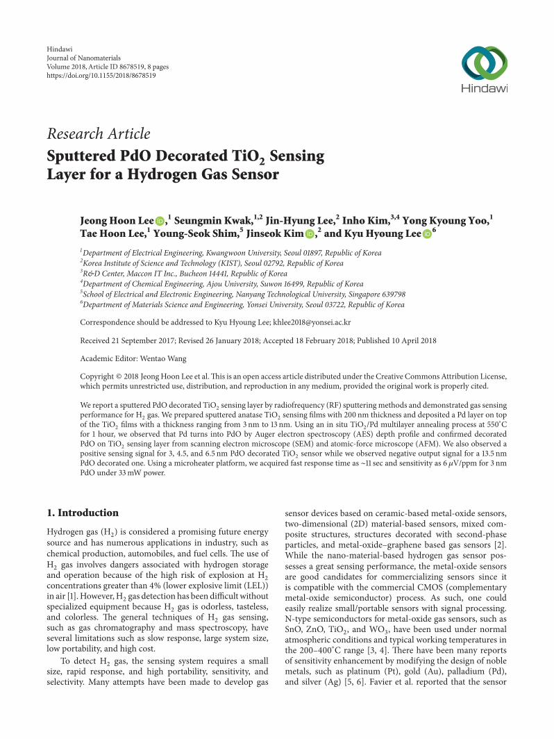
Figure 1 shows the XRD patterns of the (a) TiO2films and
(b) PdO NPs decorated TiO2film with four PdO different
thicknesses. In Figure 1(a), the XRD patterns exhibited strongdiffraction peaks at 25.4∘ and 48∘ which indicated the mainpeaks of the anatase (101).We calculated the average grain sizeof the TiO
2using XRD peak broadening based on the Scher-
rer formula [16]. The observed particle size of 200 nm thickTiO2thin film layer was a nanometer scale of approximately
4.8 nm. Figure 1(b) demonstrates the XRD patterns of thePdONPs decorated TiO
2film with different PdO thicknesses
ranging from 0 to 13 nm.We deposited in situ TiO2and Pd by
using magnetron reactive sputtering and annealed TiO2/Pd
multilayered samples in an atmospheric environment tubefurnace at 550∘C for 1 hour. After the annealing process,we confirmed the formation of PdO (index: red diamond inFigure 1(b)). When the thickness of PdO increased, the mainpeak of PdO 2𝜃 = 33.8∘ was also increased, which indicatedan improvement in the crystallization of the PdO thin films. Aclear detectable peak of the PdO phase can be observed in theXRD pattern, even at 3 nmPdO thickness. Lallo et al. claimedthat the Pd oxidation condition depends on the amountof deposited Pd. Thicker Pd deposits behaved similarly tobulk Pd samples, whereas the oxidation temperatures may be
Journal of Nanomaterials 3
10 20 30 40 50 60 70 80 90
(215
)(2
20)
Inte
nsity
(a. u
.)
(101
)
(103
) (200
)
(105
) (211
)
(204
)
(116
)(004
)(1
12)
TiO2 films
2�휃
(a)
10 20 30 40 50 60 70 80 90
Inte
nsity
(a.u
.)
(116
)(2
20)
(215
)
(211
)
(112
)(0
04)
(204
)
(103
)
(200
)
(105
)(101
)
(202
)(200
)(1
03)
(112
)
(110
)
(100
)
(101
)
P0-T 0 nm Pd
P3-T
P4.5-T
P6.5-T
P13-T
3 nm Pd
4.5 nm Pd
6.5 nm Pd
13 nm Pd
2�휃
: TiO2: Pdo
(b)
Figure 1: The XRD patterns of (a) TiO2films and (b) PdO NPs decorated TiO
2film with four PdO different thicknesses.
PdO 3 nm PdO 4.5 nm
PdO 6.5 nm PdO 13 nm
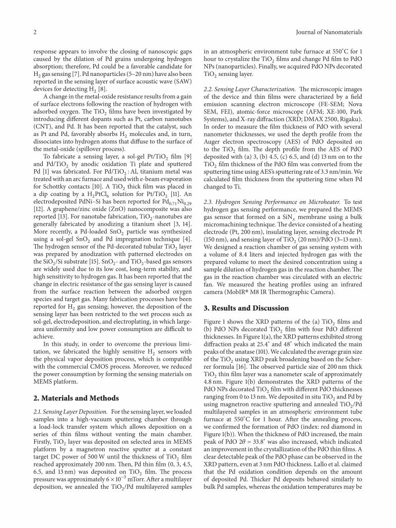
Figure 2: The SEM images of the PdO NPs decorated TiO2film
(PdO thickness: 3, 4.5, 6.5, and 13 nm).
reduced for thinner films [17].We confirmed that the Pd filmsafter annealing at 550∘C for 1 hour were completely oxidizedto PdO.
The SEM images of the PdO NPs decorated TiO2film
are shown in Figure 2. The film thickness was calculated as3.0, 4.5, 6.5, and 13 nm using a depth profile from the AES(see Figure 4). We clearly observed grain growth with anincrease in the PdO film thickness. It is generally acceptedthat the presence of PdO (or Pd) particles or films is essentialto achieve high sensitivity for H
2gas sensing. After a 3 nm
deposition, we observed clear PdO grain formation on theTiO2films, and the grain size increased with the PdO thick-
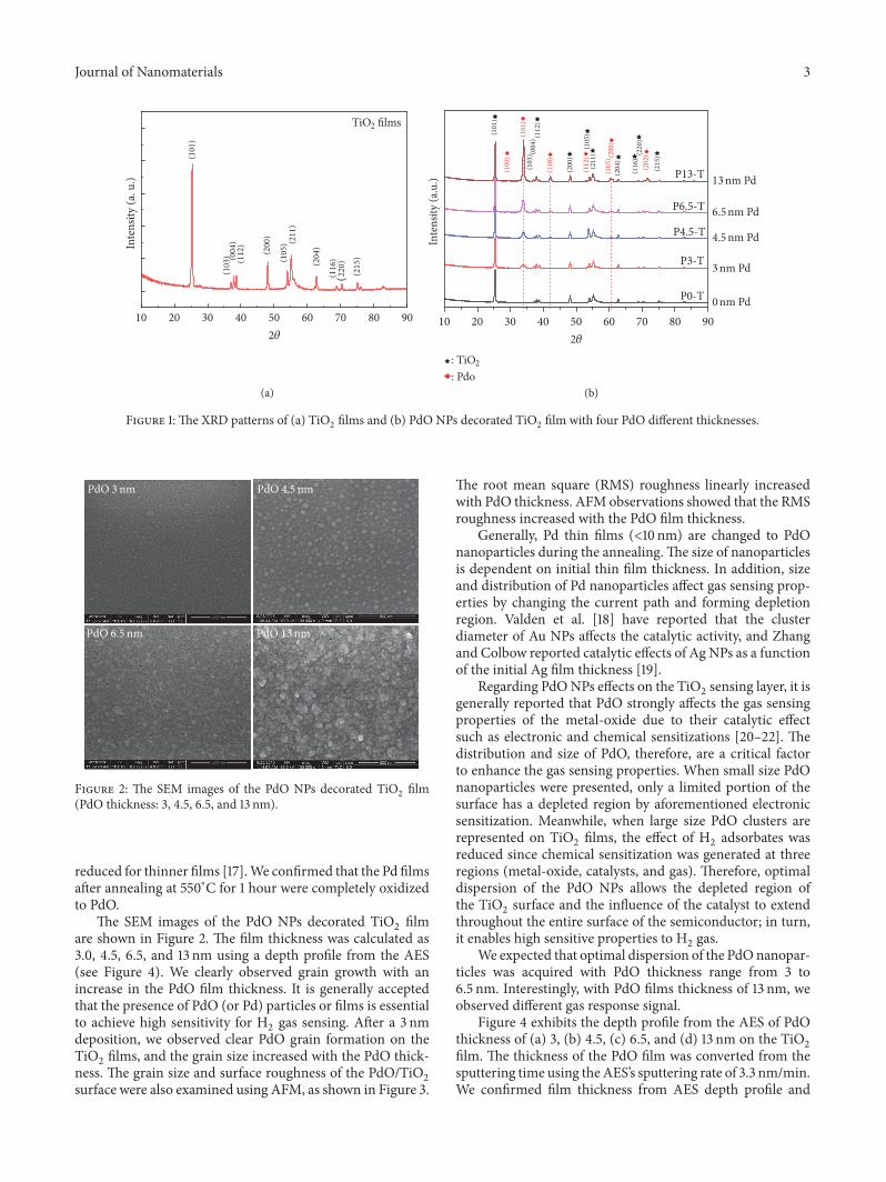
ness. The grain size and surface roughness of the PdO/TiO2
surface were also examined using AFM, as shown in Figure 3.
The root mean square (RMS) roughness linearly increasedwith PdO thickness. AFM observations showed that the RMSroughness increased with the PdO film thickness.
Generally, Pd thin films (<10 nm) are changed to PdOnanoparticles during the annealing.The size of nanoparticlesis dependent on initial thin film thickness. In addition, sizeand distribution of Pd nanoparticles affect gas sensing prop-erties by changing the current path and forming depletionregion. Valden et al. [18] have reported that the clusterdiameter of Au NPs affects the catalytic activity, and Zhangand Colbow reported catalytic effects of Ag NPs as a functionof the initial Ag film thickness [19].
Regarding PdONPs effects on the TiO2sensing layer, it is
generally reported that PdO strongly affects the gas sensingproperties of the metal-oxide due to their catalytic effectsuch as electronic and chemical sensitizations [20–22]. Thedistribution and size of PdO, therefore, are a critical factorto enhance the gas sensing properties. When small size PdOnanoparticles were presented, only a limited portion of thesurface has a depleted region by aforementioned electronicsensitization. Meanwhile, when large size PdO clusters arerepresented on TiO
2films, the effect of H
2adsorbates was
reduced since chemical sensitization was generated at threeregions (metal-oxide, catalysts, and gas). Therefore, optimaldispersion of the PdO NPs allows the depleted region ofthe TiO
2surface and the influence of the catalyst to extend
throughout the entire surface of the semiconductor; in turn,it enables high sensitive properties to H
2gas.
We expected that optimal dispersion of the PdOnanopar-ticles was acquired with PdO thickness range from 3 to6.5 nm. Interestingly, with PdO films thickness of 13 nm, weobserved different gas response signal.
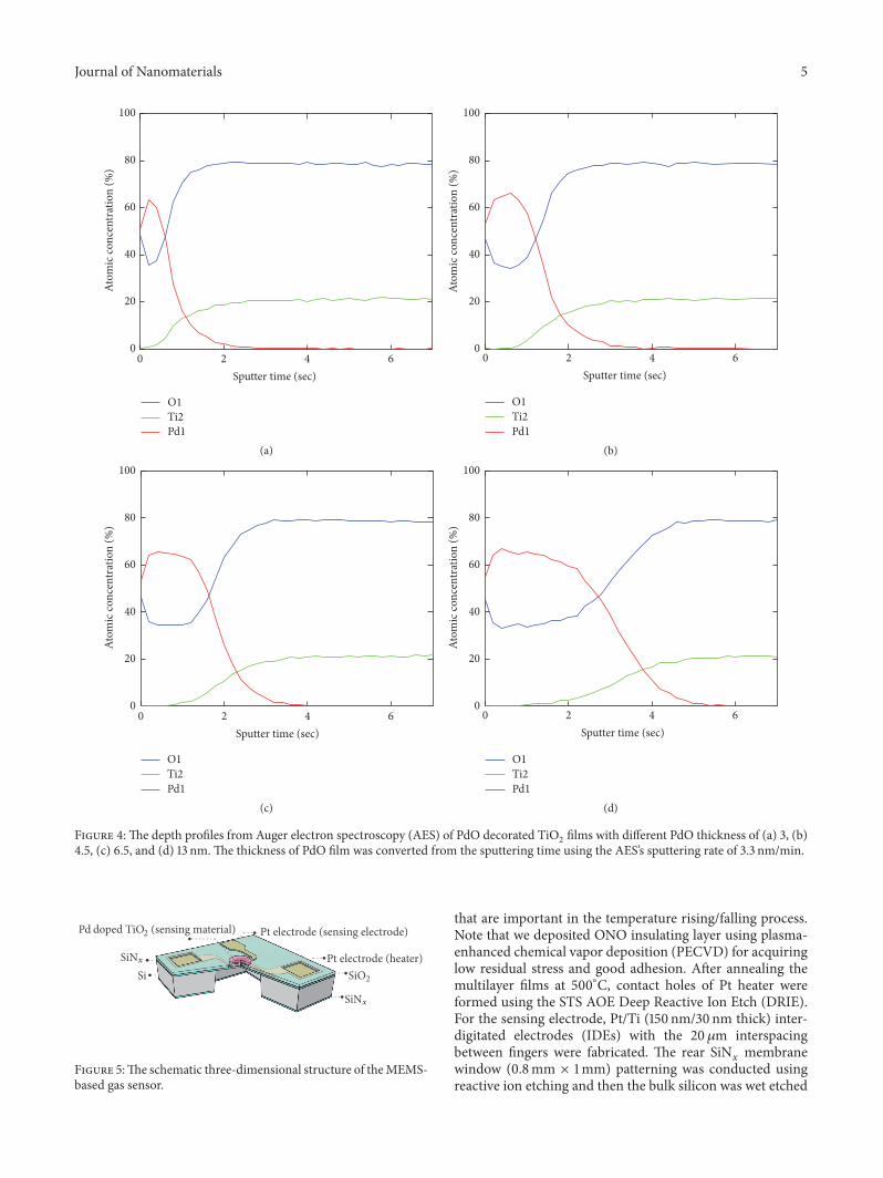
Figure 4 exhibits the depth profile from the AES of PdOthickness of (a) 3, (b) 4.5, (c) 6.5, and (d) 13 nm on the TiO
2
film. The thickness of the PdO film was converted from thesputtering time using theAES’s sputtering rate of 3.3 nm/min.We confirmed film thickness from AES depth profile and
4 Journal of Nanomaterials
0 3 6 9 12 15
2
4
6
8
Roug
hnes
s (nm
)
Thickness of deposited Pd thin film (nm)
PdO 3 nm PdO 4.5 nm
PdO 6.5 nm PdO 13 nm
Figure 3: The graph of RMS surface roughness along with different PdO thickness and AFM images of PdO NPs decorated TiO2film.
calculated the interface of PdO and TiO2which was 3, 4.5,
6.5, and 13 nm, respectively. After deposition of the Pd thinfilm, we annealed the Pd/TiO
2films at 550∘C for 1 hour in
an air atmosphere and acquired the PdONPs decorated TiO2
films.The schematic three-dimensional structure of the pro-
posed MEMS-based gas sensor is shown in Figure 5. Forfabricating MEMS-based gas sensor, using low pressurechemical vapor deposition process (LPCVD), we deposited
a SiN𝑥film (2 𝜇m thick) on a p-type Si (100) substrate.
Then we deposited 200 nm thick Pt film that was used formicroheater. Note that a 10 nm thick Ti film was used foradhesion layer to increase the adhesion properties betweenSiN𝑥and Pt. The Pt heater was patterned using standard
photolithography and then etched using reactive ion etcher(RIE). Here, we used an ONO insulating layer made of aSiO2(500 nm)/SiN
𝑥(250 nm)/SiO
2(250 nm) structure on Pt
heater to acquire thermal stability and mechanical stability
Journal of Nanomaterials 5
0 2 4 60
20
40
60
80
100At
omic
conc
entr
atio
n (%
)
Sputter time (sec)
O1Ti2Pd1
(a)
0 2 4 60
20
40
60
80
100
Atom
ic co
ncen
trat
ion
(%)
Sputter time (sec)
O1Ti2Pd1
(b)
0 2 4 60
20
40
60
80
100
Atom
ic co
ncen
trat
ion
(%)
Sputter time (sec)
O1Ti2Pd1
(c)
0 2 4 60
20
40
60
80
100At
omic
conc
entr
atio
n (%
)
Sputter time (sec)
O1Ti2Pd1
(d)
Figure 4: The depth profiles from Auger electron spectroscopy (AES) of PdO decorated TiO2films with different PdO thickness of (a) 3, (b)
4.5, (c) 6.5, and (d) 13 nm. The thickness of PdO film was converted from the sputtering time using the AES’s sputtering rate of 3.3 nm/min.
SiO2
SiNx
SiNx
SiPt electrode (heater)
Pd doped TiO2 (sensing material) Pt electrode (sensing electrode)
Figure 5:The schematic three-dimensional structure of theMEMS-based gas sensor.
that are important in the temperature rising/falling process.Note that we deposited ONO insulating layer using plasma-enhanced chemical vapor deposition (PECVD) for acquiringlow residual stress and good adhesion. After annealing themultilayer films at 500∘C, contact holes of Pt heater wereformed using the STS AOE Deep Reactive Ion Etch (DRIE).For the sensing electrode, Pt/Ti (150 nm/30 nm thick) inter-digitated electrodes (IDEs) with the 20 𝜇m interspacingbetween fingers were fabricated. The rear SiN
𝑥membrane
window (0.8mm × 1mm) patterning was conducted usingreactive ion etching and then the bulk silicon was wet etched
6 Journal of Nanomaterials
Time (sec)0 100 200 300 400 500 600 700 800 900 1000
dV o
ut (m
V)
1.0
1.5
2.0
2.5
3.0
3.5
4.0
4.5
5.0100 ppm 200 ppm 300 ppm
(a)
Time (sec)0 200 400 600 800
100 ppm 200 ppm 300 ppm
dV o
ut (m
V)
0
2
4
6
8
(b)
Time (sec)0 200 400 600 800 1000
100 ppm 200 ppm 300 ppm
dV o
ut (m
V)
0
2
4
6
8
(c)
0 100 200 300 400 500 600 700 800 900500
1000
1500
2000
dV o
ut (m
V)
Time (sec)
33 mWAirpurging400 ppm
(d)
Figure 6: The time sequential sensor signal output with heater power consumption. The H2gas concentration of 100, 200, and 400 ppm was
sequentially applied to the PdO decorated TiO2films with PdO thickness of (a) 3, (b) 4.5, (c) 6.5, and (d) 13 nm on the TiO
2film.
with a KOH silicon etchant. Finally, we cut the wafer intounit sensors (2.5mm× 2.5mm)with awafer sawingmachine.When we applied voltage across the Pt heaters on unitsensors, the temperature rapidly increased and then quicklydropped when the voltage was removed.
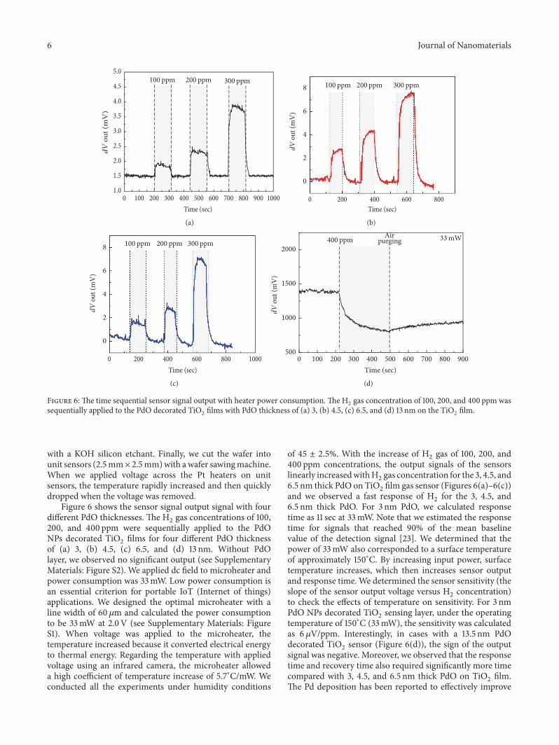
Figure 6 shows the sensor signal output signal with fourdifferent PdO thicknesses. The H
2gas concentrations of 100,
200, and 400 ppm were sequentially applied to the PdONPs decorated TiO
2films for four different PdO thickness
of (a) 3, (b) 4.5, (c) 6.5, and (d) 13 nm. Without PdOlayer, we observed no significant output (see SupplementaryMaterials: Figure S2). We applied dc field to microheater andpower consumption was 33mW. Low power consumption isan essential criterion for portable IoT (Internet of things)applications. We designed the optimal microheater with aline width of 60 𝜇m and calculated the power consumptionto be 33mW at 2.0V (see Supplementary Materials: FigureS1). When voltage was applied to the microheater, thetemperature increased because it converted electrical energyto thermal energy. Regarding the temperature with appliedvoltage using an infrared camera, the microheater alloweda high coefficient of temperature increase of 5.7∘C/mW. Weconducted all the experiments under humidity conditions
of 45 ± 2.5%. With the increase of H2gas of 100, 200, and
400 ppm concentrations, the output signals of the sensorslinearly increasedwithH
2gas concentration for the 3, 4.5, and
6.5 nm thick PdO on TiO2film gas sensor (Figures 6(a)–6(c))
and we observed a fast response of H2for the 3, 4.5, and
6.5 nm thick PdO. For 3 nm PdO, we calculated responsetime as 11 sec at 33mW. Note that we estimated the responsetime for signals that reached 90% of the mean baselinevalue of the detection signal [23]. We determined that thepower of 33mW also corresponded to a surface temperatureof approximately 150∘C. By increasing input power, surfacetemperature increases, which then increases sensor outputand response time. We determined the sensor sensitivity (theslope of the sensor output voltage versus H
2concentration)
to check the effects of temperature on sensitivity. For 3 nmPdO NPs decorated TiO
2sensing layer, under the operating
temperature of 150∘C (33mW), the sensitivity was calculatedas 6 𝜇V/ppm. Interestingly, in cases with a 13.5 nm PdOdecorated TiO
2sensor (Figure 6(d)), the sign of the output
signal was negative. Moreover, we observed that the responsetime and recovery time also required significantly more timecompared with 3, 4.5, and 6.5 nm thick PdO on TiO
2film.
The Pd deposition has been reported to effectively improve
Journal of Nanomaterials 7
the hydrogen sensing abilities of the sensor because of thecatalytic effect of Pd [24]. The catalyst, such as Pt and Pd,favorably absorbed the H
2molecules, which then dissociated
into H atoms that diffused to the surface of the metal-oxide(spillover process) [25]. For 13.5 nm thick Pd film, we expectthat they did not change to discontinuous NPs; in turn, theystill fully covered TiO
2film surface, leading to inactive TiO
2
surface toH2gas. In the case of the PdO layer with a thickness
of 13.5 nm, the sensing layer acts as a sensing layer, not acatalyst layer, so that the sensing signal appears to be oppositeto that of the PdO layer having a thickness of 3, 4.5, and6.5 nm.
The H2sensing mechanisms of Pd- (PdO-) based sensors
can be classified into two categories [26]. Firstly, in case ofpresenting of nanogap structure (discontinuous structure),when a Pd structure is exposed to H
2, a Pd/H solid solution is
formed at low H2concentrations. At high concentrations of
H2, there is a 3.5% volume expansion due to the numerous H
atoms incorporated into Pd. Since nanogaps in Pd structuresinterfere with electric current flow, volume expansion afterH2exposure allows the nanogaps to be closed, leading to
a substantial inflow of electrical current. As a result, theelectrical resistance (conduction) of H
2sensors abruptly
decreases (increases) when exposed to H2and recovers to the
initial base resistance (base conduction is zero) after removalof H2. Secondly, in contrast to presenting nanogap, H atoms
can be incorporated into the continuous Pd structures andact as electron scattering sources, so that electrical resistanceincreases. In this case, the electrical resistance increaseswith increase in H
2concentration, because the frequency of
electron-H scattering increases as the amount of H atoms inthe Pd structures increases.
4. Conclusion
To conclude, our findings provide a methodology for thedeposition of H
2sensing thin films of PdO NPs decorated
TiO2films using sputtering. Subsequent thin film charac-
terization using XRD, SEM, AFM, and AES depth profileswas used to observe the deposition parameters for PdONPs decorated TiO
2films. It was found that the sputtering
thickness of the catalytic PdO layer greatly influenced thesurfacemorphology, which resulted in gas sensing properties.We acquired the sensitivity as +6𝜇V/ppm for 3 nm PdOdecorated TiO
2sensor under 33mW power consumption
while the sign of the output signal was negative for 13.5 nmPdO decorated TiO
2sensor.
Conflicts of Interest
The authors declare that there are no conflicts of interestregarding the publication of this paper.
Authors’ Contributions
Jeong Hoon Lee and Seungmin Kwak have equally con-tributed to this paper.
Acknowledgments
This work was supported by a National Research Foundationof Korea grant funded by the Korean government (MEST;NRF-2015R1D1A1A01059806) and by a grant of the KoreaHealth Technology R&D Project through the Korea HealthIndustry Development Institute (KHIDI), funded by theMinistry of Health andWelfare, Republic of Korea (Grant no.HI16C0272). The work reported in this paper was conductedduring the sabbatical year of Kwangwoon University in 2015.
Supplementary Materials
Supplementary information for this article can be found inthe attached file. Figure S1: (a) IRmeasurement set-up and (b)measured temperature by IR camera as function of appliedvoltage. Figure S2: hydrogen gas detection without PdO layer.(Supplementary Materials)
References
[1] A. Mirzaei, S. G. Leonardi, and G. Neri, “Detection of haz-ardous volatile organic compounds (VOCs) by metal oxidenanostructures-based gas sensors: A review,” Ceramics Interna-tional, vol. 42, no. 14, pp. 15119–15141, 2016.
[2] Z. Dai, L. Xu, G. Duan et al., “Fast-response, sensitivitive andlow-powered chemosensors by fusing nanostructured porousthin film and IDEs-microheater chip,” Scientific Reports, vol. 3,article no. 1669, 2013.
[3] C. Rossi, E. Scheid, and D. Esteve, “Theoretical and experimen-tal study of silicon micromachined microheater with dielectricstacked membranes,” Sensors and Actuators A: Physical, vol. 63,no. 3, pp. 183–189, 1997.
[4] Y. Cui, “Nanowire nanosensors for highly sensitive and selectivedetection of biological and chemical species,” Science, vol. 293,no. 5533, pp. 1289–1292.
[5] A. Wisitsoraat, A. Tuantranont, E. Comini, G. Sberveglieri,and W. Wlodarski, “Characterization of n-type and p-typesemiconductor gas sensors based on NiOx doped TiO2 thinfilms,”Thin Solid Films, vol. 517, no. 8, pp. 2775–2780, 2009.
[6] H. Gu, Z. Wang, and Y. Hu, “Hydrogen gas sensors based onsemiconductor oxide nanostructures,” Sensors, vol. 12, no. 5, pp.5517–5550, 2012.
[7] F. Favier, E. C. Walter, M. P. Zach, T. Benter, and R. M.Penner, “Hydrogen sensors and switches from electrodepositedpalladium mesowire arrays,” Science, vol. 293, no. 5538, pp.2227–2231, 2001.
[8] D. Sil, J. Hines, U. Udeoyo, and E. Borguet, “PalladiumNanoparticle-Based Surface Acoustic Wave Hydrogen Sensor,”ACS AppliedMaterials & Interfaces, vol. 7, no. 10, pp. 5709–5714,2015.
[9] X. Bevenot, A. Trouillet, C. Veillas, H. Gagnaire, and M.Clement, “Hydrogen leak detection using an optical fibre sensorfor aerospace applications,” Sensors and Actuators B: Chemical,vol. 67, no. 1, pp. 57–67, 2000.
[10] C. Xiang, Z. She, Y. Zou et al., “A room-temperature hydrogensensor based on Pd nanoparticles doped TiO2 nanotubes,”Ceramics International, vol. 40, pp. 16343–16348, 2014.
[11] P. Bhattacharyya, P. K. Basu, B. Mondal, and H. Saha, “A lowpower MEMS gas sensor based on nanocrystalline ZnO thin
8 Journal of Nanomaterials
films for sensing methane,” Microelectronics Reliability, vol. 48,no. 11-12, pp. 1772–1779, 2008.
[12] P. Bhattacharyya, “Technological journey towards reliablemicroheater development for MEMS gas sensors: a review,”IEEE Transactions on Device and Materials Reliability, vol. 14,no. 2, pp. 589–599, 2014.
[13] J. H. Lee, K. S. Hwang, and T. S. Kim, “Microstress relax-ation effect of Pb(Zr0.52Ti0.48) O3 films with thicknesses formicro/nanopiezoelectric device,” Applied Physics Letters, vol.96, no. 9, Article ID 092904, 2010.
[14] P. C. H. Chan, G.-Z. Yan, L.-Y. Sheng et al., “An integrated gassensor technology using surfacemicro-machining,” Sensors andActuators B: Chemical, vol. 82, no. 2-3, article no. 4200, pp. 277–283, 2002.
[15] X. Chen, C. K. Y. Wong, C. A. Yuan, and G. Zhang, “Nanowire-based gas sensors,” Sensors and Actuators B: Chemical, vol. 177,pp. 178–195, 2013.
[16] L. C. Tien, H. T. Wang, B. S. Kang et al., “Room-temperaturehydrogen-selective sensing using single Pt-coated ZnOnanowires at microwatt power levels,” Electrochemical andSolid-State Letters, vol. 8, no. 9, pp. G230–G232, 2005.
[17] J. Lallo, S. A. Tenney, A. Kramer, P. Sutter, and M. Batzill,“Oxidation of palladium on Au(111) and ZnO(0001) supports,”The Journal of Chemical Physics, vol. 141, no. 15, Article ID154702, 2014.
[18] M. Valden, X. Lai, and D. W. Goodman, “Onset of catalyticactivity of gold clusters on titania with the appearance ofnonmetallic properties,” Science, vol. 281, no. 5383, pp. 1647–1650, 1998.
[19] J. Zhang and K. Colbow, “Surface silver clusters as oxidationcatalysts on semiconductor gas sensors,” Sensors and ActuatorsB: Chemical, vol. 40, no. 1, pp. 47–52, 1997.
[20] Y.-S. Shim, H. G. Moon, D. H. Kim et al., “Au-decorated WO3cross-linked nanodomes for ultrahigh sensitive and selectivesensing of NO2 and C2H5OH,” RSC Advances, vol. 3, no. 26,pp. 10452–10459, 2013.
[21] E. Comini, G. Faglia, G. Sberveglieri, Z. Pan, and Z. L. Wang,“Stable and highly sensitive gas sensors based on semiconduct-ing oxide nanobelts,” Applied Physics Letters, vol. 81, no. 10, pp.1869–1871, 2002.
[22] X. Liu, J. Zhang, T. Yang, X. Guo, S.Wu, and S.Wang, “Synthesisof Pt nanoparticles functionalizedWO3 nanorods and their gassensing properties,” Sensors and Actuators B: Chemical, vol. 156,no. 2, pp. 918–923, 2011.
[23] K. Kalantar-Zadeh, “Sensors: An introductory course,” Sensors:An Introductory Course, vol. 9781461450528, pp. 1–196, 2013.
[24] J. Moon, H.-P. Hedman, M. Kemell, A. Tuominen, and R.Punkkinen, “Hydrogen sensor of Pd-decorated tubular TiO
2
layer prepared by anodization with patterned electrodes onSiO2/Si substrate,” Sensors and Actuators B: Chemical, vol. 222,
Article ID 18909, pp. 190–197, 2016.[25] B. Liu, D. Cai, Y. Liu et al., “High-performance room-
temperature hydrogen sensors based on combined effects of Pddecoration and Schottky barriers,” Nanoscale, vol. 5, no. 6, pp.2505–2510, 2013.
[26] J. Lee, W. Shim, J.-S. Noh, and W. Lee, “Design rules fornanogap-based hydrogen gas sensors,” ChemPhysChem, vol. 13,no. 6, pp. 1395–1403, 2012.

CorrosionInternational Journal of
Hindawiwww.hindawi.com Volume 2018
Advances in
Materials Science and EngineeringHindawiwww.hindawi.com Volume 2018
Hindawiwww.hindawi.com Volume 2018
Journal of
Chemistry
Analytical ChemistryInternational Journal of
Hindawiwww.hindawi.com Volume 2018
Scienti�caHindawiwww.hindawi.com Volume 2018
Polymer ScienceInternational Journal of
Hindawiwww.hindawi.com Volume 2018
Hindawiwww.hindawi.com Volume 2018
Advances in Condensed Matter Physics
Hindawiwww.hindawi.com Volume 2018
International Journal of
BiomaterialsHindawiwww.hindawi.com
Journal ofEngineeringVolume 2018
Applied ChemistryJournal of
Hindawiwww.hindawi.com Volume 2018
NanotechnologyHindawiwww.hindawi.com Volume 2018
Journal of
Hindawiwww.hindawi.com Volume 2018
High Energy PhysicsAdvances in
Hindawi Publishing Corporation http://www.hindawi.com Volume 2013Hindawiwww.hindawi.com
The Scientific World Journal
Volume 2018
TribologyAdvances in
Hindawiwww.hindawi.com Volume 2018
Hindawiwww.hindawi.com Volume 2018
ChemistryAdvances in
Hindawiwww.hindawi.com Volume 2018
Advances inPhysical Chemistry
Hindawiwww.hindawi.com Volume 2018
BioMed Research InternationalMaterials
Journal of
Hindawiwww.hindawi.com Volume 2018
Na
nom
ate
ria
ls
Hindawiwww.hindawi.com Volume 2018
Journal ofNanomaterials
Submit your manuscripts atwww.hindawi.com