springer978-3-642-35792...editors: b. bhushan, h. fuchs, s. hosaka 2004 nanostructures theory and...
TRANSCRIPT

NANOSCIENCE AND TECHNOLOGY
Springer Berlin Heidelberg New York Hong Kong London Milan Paris Tokyo
Physics and Astronomy springeronline.com
ONLINE LIBRARY
NANOSCIENCE AND TECHNOLOGY
Series Editors: P. Avoris K. von Klitzing H. Sakaki R. Wiesendanger
The series NanoScience and Technology is focused on the fascinating nano-world, mesoscopic physics, analysis with atomic resolution, nano and quantum-effect devices, nanomechanics and atomic-scale processes. All the basic aspects and technology-oriented developments in this emerging discipline are covered by comprehensive and timely books. The series constitutes a survey of the relevant special topics, which are presented by leading experts in the field. These books will appeal to researchers, engineers, and advanced students.
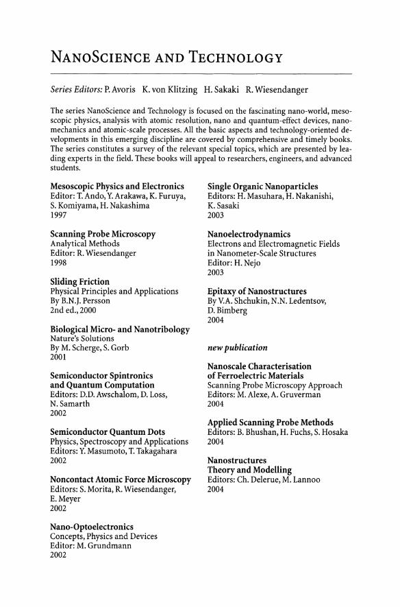
Mesoscopic Physics and Electronics Editor: T. Ando, Y. Arakawa, K. Furuya, S. Komiyama, H. Nakashima 1997
Scanning Probe Microscopy Analytical Methods Editor: R. Wiesendanger 1998
Sliding Friction Physical Principles and Applications By B.N.}. Persson 2nd ed., 2000
Biological Micro- and Nanotribology Nature's Solutions By M. Scherge, S. Gorb 2001
Semiconductor Spintronics and Quantum Computation Editors: D.D. Awschalom, D. Loss, N.Samarth 2002
Semiconductor Quantum Dots Physics, Spectroscopy and Applications Editors: Y. Masumoto, T. Takagahara 2002
Noncontact Atomic Force Microscopy Editors: S. Morita, R. Wiesendanger, E.Meyer 2002
Nano-Optoelectronics Concepts, Physics and Devices Editor: M. Grundmann 2002
Single Organic Nanopartides Editors: H. Masuhara, H. Nakanishi, K. Sasaki 2003
Nanoelectrodynamics Electrons and Electromagnetic Fields in Nanometer-Scale Structures Editor: H. Nejo 2003
Epitaxy of Nanostructures By v'A. Shchukin, N.N. Ledentsov, D.Bimberg 2004
new publication
Nanoscale Characterisation of Ferroelectric Materials Scanning Probe Microscopy Approach Editors: M. Alexe, A. Gruverman 2004
Applied Scanning Probe Methods Editors: B. Bhushan, H. Fuchs, S. Hosaka 2004
Nanostructures Theory and Modelling Editors: Ch. Delerue, M. Lannoo 2004
Bharat Bhushan Harald Fuchs Sumio Hosaka
Applied Scanning Probe Methods
With 338 Figures
Including 6 Color Figures
Springer
Professor Bharat Bhushan The Ohio State University, Department of Mechanical Engineering, 206 W. 18th Avenue, Columbus, Ohio 43210-1107 e-mail: [email protected]
Professor Dr. Harald Fuchs Universitat Miinster, Wilhelm-Klemm-Str. 10,48149 Miinster, Germany e-mail: [email protected]
Professor Dr. Sumio Hosaka Gunma University, Dept. Electronic Engineering, 1-5-1 Tenjin-cho, 376-8515 Kiryu-City e-mail: [email protected]
Series Editors: Professor Dr. Phaedon Avouris IBM Research Division, Nanometer Scale Science & Technology Thomas J. Watson Research Center, P.O. Box 218 Yorktown Heights, NY 10598, USA
Professor Dr., Dres. h. c. Klaus von Klitzing Max-Planck-Institut fiir Festkorperforschung, Heisenbergstrasse 1 70569 Stuttgart, Germany
Professor Hiroyuki Sakaki Universitiy of Tokyo, Institute of Industrial Science,4-6-1 Komaba, Meguro-ku Tokyo 153-8505, Japan
Professor Dr. Roland Wiesen danger Insitut fiir Angewandte Physik, Universitat Hamburg, Jungiusstrasse 1 20355 Hamburg, Germany
ISSN 1434-4904 ISBN 978-3-540-00527-8 Springer Verlag Berlin Heidelberg New York
Library of Congress Cataloging-in-Publication Data Applied scanning probe methods I Bharat Bhushan, Harald Fuchs, Sumio Hosaka [eds.l.
p. cm. - (Nanoscience and technology) Includes bibliographical references and index.
1. Materials-Microscopy. 2. Scanning probe microscopy. I. Bhushan, Bharat, 1949- II. Fuchs, H. (Harald) III. Hosaka, Sumio. IV. Series.
TA417.23.A6552003 620.1'1299-dc22
2003059049
This work is subject to copyright. All rights are reserved, whether the whole or part of the material is concerned, specifically the rights of translation, reprinting, reuse of illustrations, recitation, broadcasting, reproduction on microfilm or in any other way, and storage in data banks. Duplication of this publication or parts thereof is permitted only under the provisions of the German Copyright Law of September 9, 1965, in its current version, and permission for use must always be obtained from Springer-Verlag. Violations are liable for prosecution under the German Copyright Law.
Springer-Verlag is a part of Springer Science+Business Media springeronline.com
© Springer-Verlag Berlin Heidelberg 2004
The use of general descriptive names, registered names, trademarks, etc. in this publication does not imply, even in the absence of a specific statement, that such names are exempt from the relevant protective laws and regulations and therefore free for general use.
Product liability: The publishers cannot guarantee the accuracy of any information about dosage and application contained in this book. In every individual case the user must check such information by consulting the relevant literature.
Typesetting: Fotosatz-Service Kohler GmbH, Wiirzburg Coverdesign: design & production, Heidelberg
Printed on acid-free paper 2/3020xv - 5432 1 0
Preface
Since introduction ofthe Scanning Tunnelling Microscope (STM) by inventors G. Binnig and H. Rohrer in 1981 at the IBM Zurich Research Laboratory, Ruschlikon, Switzerland., many variations of tip probe based microscopies, referred to as Scanning Probe Microscopies (SPM) have been developed. Nanoscale Science and Technology are strongly driven by SPMs which allow investigation and manipulation of surfaces down to the atomic scale. While the pure imaging capabilities of SPM techniques dominated the application of these methods at their early development stages, the physics of probe-sample interactions and the quantitative analyses of elastic/plastic, tribological, electronic, magnetic, biological, and chemical surfaces have now become of increasing interest. With growing understanding of the underlying interaction mechanisms, SPMs have found applications in many fields outside basic research fields. In addition, a variety of derivatives of all these methods has been developed for special applications, some of them targeting far beyond microscopy.
For industrial applications, the large SPM-subfamily of Scanning Force Microscopy (SFM) exhibiting atomic resolution capability is of special interest. Originally denoted as Atomic Force Microscopy (AFM), the basic instrument was invented by G. Binnig, C. Quate and Ch. Gerber in 1986. The introduction of this technique was a direct consequence of the observation of sizable interaction forces between a near field probe and a sample surface which were already seen in earlier experiments done with Scanning Tunnelling Microscopy (STM). STM experiments performed, for example, on HOPG-graphite surfaces, indicated a strong influence of elastic surface properties on the measured surface corrugation which could not be traced back to electronic surface properties. Based on these types of results it appeared quite natural to introduce a method that is solely based on tipsample force interactions rather than transport phenomena such as electron tunnelling as used in the STM. The AFM was the first purely force sensitive microscope. Its applicability on electrically insulating surfaces opened a wide range of applications. In addition, this method can also be applied under various environmental conditions, such as vacuum, air and liquids. Thus, a wide variety of applications including industrial quality control and the investigation ofliving biological materials became feasible with high resolution, and without any conductive coatings. Since for many practical applications atomic resolution is not the ultimate and only goal, the family of commercial instruments which measure forces is more generally referred to as Scanning Force Microscopes (SFMs). While in the beginning of SFMs, high resolution measurement of surface topography was the major
VI Preface
application, it became clear very soon, that by applying more complex strategies, i.e. dynamic and lateral force techniques the quantitative measurement oflocal material properties also became possible. Beyond that, the local measurement of the distribution oflocally varying electrical surface potentials and magnetic stray fields became accessible - altogether properties of great practical interest. Therefore, is appears quite natural that SFM related techniques playa major role in industrial applications today including topographic and dynamical surface studies such as of semiconductors, polymers, paper, ceramics, magnetic and biological materials.
Commercial production of SPMs started with STM in 1988 and has grown to several hundred million dollars industry. The number of these instruments is equally divided among the U.S., Japan and Europe with the following industry, university and government laboratories split: 50150, 70/30, and 30/70, respectively.
This book selects some representative recent applications of SPM with a focus on practical applications. While not necessarily limited to SFM, the general applicability and variability of this method in industrial research and quality control led to a natural focus as reflected in the large number of chapters dealing with SFM related techniques. Selected articles on the application of near field optical and capacitance techniques for novel storage applications put a special focus on industrial R&D based on these techniques. The organization of the book is straightforward. The book is divided into three parts. Part I contains chapters dealing with the theoretical background of static and dynamic force microscopies including sensor technology and methods for tip characterization. Part II contains chapters on applications of scanning force microscopy such as micro- and nanotribology, polymer surfaces, stray field measurements and roughness investigations. The last Part III contains a selection of articles mainly written by industrial researchers. Examples for special application ofSFM such as atomic manipulation and surface modification are presented. Furthermore, novel concepts for high resolution optical storage techniques as well as for the production of single electron devices based on SFM are presented.
The purpose of this book is to give both, a systematic physical and technical background for the academic researcher on recent progress of applied scanning probe microscopy and an overview of the current state ofSPM applications for the industrial researcher and engineer. We hope that readers find this book stimulating and productive.
We would like to thank the authors for their excellent contributions in a timely manner. We would also like to thank Dr. Marion Hertel, Senior Editor Chemistry, and Mrs. Beate Siek of Springer-Verlag for their continued support and patience during the preparation of this book.
December 2002 Prof. Dr. Bharat Bhushan, USA Prof. Dr. Harald Fuchs, Germany Prof. Dr. Sumio Hosaka, Japan
Contents
Part I
1.1
1.2
1.3
1.4 1.4.1 1.4.2
1.5
1.6
1.7
2
2.1
2.2
2.3 2.3.1 2.3.2 2.3.3
2.4
Scanning Probe Microscopy
Dynamic Force Microscopy Andre Schirmeisen, Boris Anczykowski, Harald Fuchs
Introduction
Motivation: Measurement of a Single Atomic Bond
Harmonic Oscillator: A Model System for Dynamic AFM .
Dynamic AFM Operational Modes . . . . . Amplitude-modulationltapping-mode AFM Self-Excitation Modes
Q-Control ................. .
Dissipation Processes Measured with Dynamic AFM
Conclusion
References
Interfacial Force Microscopy: Selected Applications Jack E. Houston
Introduction
The IFM Sensor
Selected Applications Adhesion ...... Nanomechanical Properties Molecular-Level Friction Studies
Conclusions
References
1
3
3
3
9
12 13 22
26
31
36
37
41
41
42
46 46 52 60
70
71
VIII
3
3.1
3.2
3.3
3.4
3.5 3.5.1 3.5.2 3.5.3
3.6 3.6.1 3.6.2 3.6.3 3.6.4 3.6.5 3.6.6
3.7 3.7.1 3.7.2
3.8 3.8.1 3.8.2
4
4.1
4.2 4.2.1
4.3 4.3.1 4.3.2
4.4 4.4.1
Atomic Force Microscopy with Lateral Modulation Volker Scherer, Michael Reinstiidtler, Walter Arnold
Introduction
Lateral Forces
Contact Mechanics
Conventional Friction Force Microscopy
Lateral Modulation Below Resonance (Visco-)Elastic Properties by Lateral Modulation Friction Properties by Lateral Modulation . . . . Lateral Modulation by Piezoelectric Transducers
Resonance Techniques .......... . Free Resonances ............. . Contact Resonances (Visco-)Elastic Contact Contact Resonances Sliding Contact "Buckling" Resonances Self Excitation ...... . Imaging Torsional Vibration
Sonolubrication . . . . . . . Theory of Out-Of-Plane Sonolubrication . Theory ofIn-Plane Sonolubrication
Related Methods .... Surface Force Apparatus Quartz Crystal Balance
Appendix 1 Appendix 2 Appendix 3
References
Sensor Technology for Scanning Probe Microscopy Egbert Oesterschulze, Rainer Kassing
Introductory Remarks . . . . . . . . .
Material Aspect of Probe Fabrication Mechanical Properties of Cantilever Probes
Scanning Near-Field Optical Microscopy Principle of Near-Field Optics ...... . Probes for Scanning Near-Field Optical Microscopy (SNOM)
Probes for Ultrafast Scanning Probe Microscopy Improved Sampling Technique
References
Contents
75
75
76
78
79
82 83 84 85
88 88 91 96 98 98 99
101 103 104
106 106 107
108 109 110
114
117
117
118 119
127 127 128
136 137
139
Contents
5
5.1
5.2
5.3 5.3.1 5.3.2 5.3.3 5.3.4
5.4 5.4.1 5.4.2 5.4.3 5.4.4 5.4.5
Tip Characterization for Dimensional Nanometrology John S. Villarrubia
Introduction . . . .
Tip Characterization Overview
Measuring Tip Shape with a Known Tip Characterizer Dilation and Erosion ........ . Reconstructing the Tip ...... . Interpreting and Checking the Result . Summary of the Method ...... .
Measuring Tip Shape without a Known Characterizer Why Does it Work? . . . . Reconstructing the Tip .. Other Modes of Operation Summary of the Method Experimental Test of Blind Reconstruction
References
IX
147
147
148
151 151 152 154 155
155 156 157 164 165 165
168
Part II Characterization . . . . . . . . . . . . . . . . . . . . . . . . . . 169
6
6.1
6.2 6.2.1 6.2.2 6.2.3 6.2.4 6.2.5 6.2.6
6.3 6.3.1 6.3.2 6.3.3
6.4 6.4.1
6.5 6.5.1 6.5.2 6.5.3
6.6
Micro/Nanotribology Studies Using Scanning Probe Microscopy Bharat Bhushan
Introduction . .
Friction and Adhesion Atomic-Scale Friction Microscale Friction . . Directionality Effect on Microfriction Velocity Dependence on Microfriction Effect of Tip Radii and Humidity on Adhesion and Friction Scale Dependence on Friction ..... .
Scratching, Wear, and Local Deformation Microscale Scratching ......... . Microscale Wear ............ . In Situ Characterization of Local Deformation
Indentation ..... . Nanoscale Indentation
Boundary Lubrication Perfluoropolyether Lubricants Self-Assembled Monolayers . Lubricant Film Thickness Measurements
Conclusions
References
171
171
173 173 173 178 181 182 183
185 185 187 190
191 191
193 193 199
.200
.202
.203
x
7
7.1
Visualization of Polymer Structures with Atomic Force Microscopy Sergei Magonov
Introduction . .
Contents
.207
.207
7.2 Basic Aspects of AFM Imaging of Polymers . 212 7.2.l Instrumentation and Operational Modes . 212 7.2.2 Sample Preparation . . . . . . . . . . . . . . 215 7.2.3 Imaging in Tapping Mode ......... . 216 7.2.4 Studies at Elevated Temperatures and in Different Environments 221
7.3 Observations of Single Macromolecules and Their Self-Assemblies 222 7.3.l Chain Molecules on Substrates . . . . . . . . . 222 7.3.2 Self-Assembly ofIndividual Macromolecules . 226 7.3.3 Thermal Motion, Adhesion, and Manipulation . 229
7.4 Studies of Semicrystalline Polymers ..... . 232 7.4.l Single Crystals of Normal Alkanes and Polyethylene . 232 7.4.2 Morphology of Semi crystalline Polymers on Surfaces and in Bulk 235 7.4.3 Lamellar Structure of Melt-Crystallized Polymers . . . . .. . 238
7.5 7.5.l 7.5.2
7.6
8
8.l
8.2 8.2.1 8.2.2 8.2.3 8.2.4
8.3 8.3.1 8.3.2
8.4
8.4.1
8.4.2 8.4.3
Compositional Imaging of Heterogeneous Polymer Systems Morphology of Block Copolymers Studies of Polymer Blends
Future Outlook
References
Displacement and Strain Field Measurements from SPM Images Jiirgen Keller, Dietmar Vogel, Andreas Schubert, Bernd Michel
Introduction . . . . . . . . . . . . . . . . . . . . . .
Basics of Digital Image Correlation ........ . Cross-Correlation Algorithms on Gray Scale Images Subpixel Analysis for Enhanced Resolution Results of Digital Image Correlation . . . . . . . . . Accuracy ...................... .
Displacement and Strain Measurements on SFM images Digital Image Correlation under SPM Conditions . . . . Technical Requirements for the Application of the Correlation Technique ........................... .
Deformation Analysis on Thermally and Mechanically Loaded Objects under the SFM . . . . . . . . . . . . . . . . . . . . Reliability Aspects of Sensors and Micro Electro-Mechanical Systems (MEMS) . . . . . . . . . . . . . Thermally Loaded Gas Sensor under SFM Crack Detection and Evaluation by SFM .
· 241 · 241 .244
.249
· 250
· 253
· 253
.254 · 255 · 257 · 259 .260
.260
.260
.262
· 263
· 263 .264 .266
Contents
8.5
8.6
9
9.1
9.2 9.2.1 9.2.2 9.2.3 9.2.4 9.2.5 9.2.6 9.2.7 9.2.8
9.3 9.3.1 9.3.2 9.3.3
9.4 9.4.1 9.4.2 9.4.3
9.5
9.6 9.6.1
10
Determination of Kinematical Properties from SFM Images
Conclusion and Outlook
Abbreviations
References
AFM Characterization of Semiconductor Line Edge Roughness Ndubuisi G. Orji, Martha I. Sanchez, Jay Raja, Theodore V. Vorburger
Introduction . . . . . .
Procedures and Algorithms Observation 1 - A Recommendation Observation 2 Observation 3 Observation 4 Observation 5 Observation 6 - A Recommendation Observation 7 - A Recommendation Observation 8 . . . . . . . . . . . .
AFM Measurement Methods . . . . Atomic Force Characterization ofPattemed Lines AFM Characterization of Line Edge Roughness New Directions .
Analysis Methods . . . RMS Roughness Linewidth Uniformity Spatial Wavelength Determination
Comparison with SEM Measurements
Future Outlook .. Physical Standards
Abbreviations
References
Mechanical Properties of Self-Assembled Organic Monolayers: Experimental Techniques and Modeling Approaches Redhouane Henda
XI
.273
.274
.274
.275
.277
.277
.279
.279
.279
.280
.280
.280
. 281
.282
.282
.282
.282
.285
.290
. 291
.292
.293
.294
.296
.298
.298
.299
.299
.303
10.1 Introduction.... . 303 10.1.1 Self-Assembled Systems . 303 10.1.2 Origin ofStiction and Mechanical Properties in Small Dimensions 305 10.1.3 Goals and Motivation ........................ 307
XII
10.2 10.2.1 10.2.2 10.2.3 10.2.4
10.3 10.3.1 10.3.2 10.3.3 10.3.4 10.3.5
10.4
10.5
11
11.1
11.2
11.2.1 11.2.2 11.2.3 11.2.4 11.2.5 11.2.6 11.2.7 11.2.8
11.3
11.4
11.5 11.5.1 11.5.2 11.5.3
Contents
Experimental Techniques .307 Introduction . . . . . . . . .307 Atomic Force Microscopy .308 Interfacial Force Microscopy .309 Analysis of Load-Displacement Curves · 310
Molecular Modeling ....... · 311 Introduction . . . . . . . . . . . . · 311 Definition of an Alkanethiol SAM · 314 Energy Minimization · 316 Molecular Dynamics · 317 Monte Carlo Method · 317
Results .. · 318
Conclusions · 323
References ...................... 324
Micro-Nano Scale Thermal Imaging Using Scanning Probe Microscopy Li Shi, Arun Majumdar
Introduction . . . . . .
Micro-Nano Scale Temperature Mapping Using Probes with Built-in Thermal Sensors ...... . STM Probes with a Built-in Thermocouple .... . Wire Thermocouple AFM Probes ......... . Individually Made Thin-Film Thermocouple Probes . Thermocouple Probes Fabricated Using Nanolithography .. Thermally Designed Batch-Fabricated Thermocouple Probes AFM Probes with a Built-in Schottky Diode ..... AFM Probes with a Built-in Resistance Thermometer . Active Thermal Feedback AFM Probes ....... .
Mechanisms of Heat Transfer between a Thermal Probe and a Sample ........ .
Imaging of Thermal Properties ........ .
Other Scanning Thermal Microscopy Methods Scanning Tunneling Thermometry .... . Thermal Expansion Thermometry .... . Near-Field Scanning Optical Thermometry
References
.327
.327
· 328 · 328 .329 .332 · 335 · 336 .340 .340 .342
.342
.346
· 353 · 353 .354 · 357
· 361
Contents
12
12.1
12.2 12.2.1 12.2.2
12.3
12.4 12.4.1 12.4.2
12.5 12.5.1 12.5.2
12.6
12.7
The Science of Beauty on a Small Scale. Nanotechnologies Applied to Cosmetic Science Gustavo Luengo, Frederic Leroy .
Introduction to Cosmetic Science
The Cosmetic Substrate: Hair and Skin and Their Modification Hair .......................... . Skin .......................... .
The SPM as a New Tool. From the Microscopic World to the Cosmetic or Sensory Perception . . . .
Recent Uses of AFM on Cosmetic Substrates Morphological Studies .... . Tribo10gical Approaches ... .
Advanced Applications of AFM Dynamic Methods ...... . Forces at the Hair Surface
The Influence of Hair and Skincare Treatments
Conclusions
References
XIII
· 363
· 363
.364
.364
.367
.369
· 371 · 371 · 373
.377
.377
.379
· 382
.384
· 385
Part III Industrial Applications ...................... 387
13
13.1
13.2 13.2.1 13.2.2 13.2.3
13.3 13.3.1 13.3.2 13.3.3 13.3.4 13.3.5
13.4 13.4.1 13.4.2
13.5 13.5.1
SPM Manipulation and Modifications and Their Storage Applications Sumio Hosaka . . . . . . . . . . . . . . . . . . . . . . . . . . .
Atomic Manipulation and Surface Modification and their Storage Application . .
Nanometer-Sized Bit Formations . . . . . . . . Field Evaporation . . . . . . . . . . . . . . . . Nano-Indentation of Probe Tip into a Sample Surface Electron Induced Local Heating and Evanescent Light Heating
Various SPM Storages [31] STM-Based Storage AFM -Based Storage . MFM-Based Storage . SNOM-Based Storage Other SPM-Based Storages
High-Speed Readout [32] Noncontact Recording .. Contact Recording ....
Possibility ofSNOM-Based Storage [4] Expectable Readout Speed ... . . . .
. 389
.390
· 390 · 391 · 398 · 401
.408
.408
.409 · 410 .411 · 412
.413
.413 · 414
· 414 · 415
XIV
13.5.2 Rotation-Type SNOM Recording System 13.5.3 Future Issues .......... .
13.6 13.6.1 13.6.2 13.6.3
13.7
14
14.1
14.2
14.3
14.4
Possibility of AFM-Based Storage . . . . Expectable Readout Speed . . . . . . . . Prototyping of Rotation-Type AFM Recording System Summary ........ .
Perspective and Summary
References
Super Density Optical Data Storage by Near-Field Optics Jun Tominaga
Introduction .
The Principle of Super-RENS
The Characteristics of Super-RENS Disks Using Sb Layers
The Proposal of Light-Scattering-Mode Super-RENS ...
Contents
· 415 · 418
· 418 · 418 · 419 .427
.427
.428
.429
.429
.429
· 431
.434
14.5 The Characteristics of Light-Scattering-Mode Super-RENS Disks 434
14.6 Summary. . 437
15
15.1 15.1.1 15.1.2 15.1.3
15.2 15.2.1 15.2.2 15.2.3
15.3
15.4 15.4.1 15.4.2 15.4.3
References
Capacitance Storage Using a Ferroelectric Medium and a Scanning Capacitance Microscope (SCM) Ryoichi Yamamoto ......... .
Introduction . . . . . . . . . . . . . . "Near-Field" Data Storage Technology Scanning Capacitance Microscope Capacitance Storage .....
A Non-Contact-Mode SCM Capacitance Detection Method Spacing Control Method Using Differential Capacitance Non-Contact Mapping of Surface Topography
Data Storage Method Using the F/S Medium ..... .
Static Characteristics of the F/S Medium ........ . Materials and Ferroelectric Properties of the F/S Medium Shift ofC-V Characteristics Using Fixed Electrodes Non-Contact Demonstration ....... .
15.5 Dynamic Characteristics of the F/S Medium 15.5.1 Dynamic Recording Characteristics 15.5.2 Bit Shape Observation .......... .
.437
.439
.439
.439
.439
.441
.442
.442
.443
.443
.444
.445
.445
.447
.448
.449
.449 · 451
Contents
15.6 Numerical Simulation Studies ofF/S Medium 15.6.1 Calculation Method ............. . 15.6.2 Capacitance Modulation of the F/S Medium .
15.7 15.7.1 15.7.2
16
16.1
16.2
16.3
16.4
16.5
Summary and Possibilities of Capacitance Storage Summary ............... . Possibilities of the Capacitance Storage
References
Room-Temperature Single-Electron Devices formed by AFM Nano-Oxidation Process Kazuhiko Matsumoto
Introduction . . . . . . . . .
AFM Nano-Oxidation Process
Single-Electron Transistor
Single-Electron Memory
Summary
References
xv
· 451 .452 .454
· 455 .455 .456
.457
.459
.459
.459
· 461
.463
.467
.467
Subject Index ................................. 469
List of Contributors
Boris Anczykowski nanoAnalytics GmbH, Gievenbecker Weg 11, 48149 Miinster, Germany e-mail: [email protected]
Walter Arnold Fraunhofer Institute for Nondestructive Testing (IZFP), University, Building 37, 66123 Saarbruecken, Germany e-mail: [email protected]
Bharat Bhushan The Ohio State University, Department of Mechanical Engineering, 206 W 18th Avenue, Columbus, Ohio 43210-1107, USA e-mail: [email protected]
Harald Fuchs UniversWit Miinster, Wilhelm-Klemm-Str. 10,48149 Miinster, Germany e-mail: [email protected]
Redhouane Henda School of Engineering, Laurentian University, Ramsey Lake Road, Sudbury, Ontario P3E 2C6, Canada e-mail: [email protected]
Sumio Hosaka Gunma University, Graduate School of Engineering Dept. Nano Material Systems, 1-5-1 Tenjin-cho, 376-8515 Kiryu-City, Japan e-mail: [email protected]
Jack E. Houston Surface & Interface Science Dept.-1114, Sandia National Laboratories, PO Box 5800, Albuquerque, NM 87185-1415, USA e-mail: [email protected]
XVIII List of Contributors
Rainer Kassing Center for Interdisciplinary Nanostructure, Science and Technology, Institut fiir Technische Physik, Universitiit Kassel, Heinrich-Plett-Str. 40, 34132 Kassel, Gennany e-mail: [email protected]
Juergen Keller Fraunhofer Institute for Reliability and Microintegration (IZM), Dept. Mechanical Reliability and Micro Materials, Gustav-Meyer-Allee 25, 13355 Berlin, Germany e-mail: [email protected]
Egbert Oesterschulze Center for Interdisciplinary Nanostructure, Science and Technology, Institut flir Technische Physik, Universitiit Kassel, Heinrich-Plett-Str. 40, 34132 Kassel, Germany e-mail: [email protected]
Frederic Leroy Physics Department, r.;OREAL Recherche, 1, Avenue Eugene Schueller, 93601 Aulnay sous Bois, France e-mail: [email protected]
Gustavo Luengo Nano-physics Laboratory, r.;OREAL Recherche, 1, Avenue Eugene Schueller, 93601 Aulnay sous Bois, France e-mail: [email protected]
Sergei Magonov Digital InstrumentsNeeco Metrology Group, 112 Robin Hill Rd., Santa Barbara, CA 93117, USA e-mail: [email protected]
Arun Majumdar Department of Mechanical Engineering, University of California at Berkeley, Berkeley, CA 94720, USA e-mail: [email protected]
Kazuhiko Matsumoto Osaka University, Institute of Scientific & Industrial Research, 8-1, Mihogaoka, Ibaraki, Osaka, 567-0047, Japan e-mail: [email protected]
List of Contributors
Bernd Michel Fraunhofer Institute for Reliability and Microintegration (lZM), Dept. Mechanical Reliability and Micro Materials, Gustav-Meyer-Allee 25, 13355 Berlin, Germany e-mail: [email protected]
Ndubuisi G. Orji NIST, 100 Bureau Drive, Stop 8212, Gaithersburg, MD 20899-8212, USA e-mail: [email protected]
Jay Raja Dept. of Mechanical Engineering and Engineering Science, University of North Carolina Charlotte, Charlotte, NC 28223, USA e-mail: [email protected]
Michael Reinstiidtler Fraunhofer Insititute for Nondestructive Testing IZFP, University, Bldg. 37 66123 Saarbruecken, Germany e-mail: [email protected]
Martha /. Sanchez IBM Almaden Research Center, 650 Harry Rd. KI7-D 1, San Jose, CA 95120-6099, USA e-mail: [email protected]
Volker Scherer
XIX
Federal Mogul, Technology Rings and Liners, Biirgermeister-Schmidt Str. 17, 51399 Burscheid, Germany e-mail: [email protected]
Andre Schirmeisen University of Miinster, Wilhelm-Klemm-Str. 10,48149 Miinster, Germany e-mail: [email protected]
Andreas Schubert Fraunhofer Institute for Reliability and Microintegration (lZM), Dept. Mechanical Reliability and Micro Materials, Gustav-Meyer-Allee 25, 13355 Berlin, Germany e-mail: [email protected]
Li Shi Department of Mechanical Engineering, ETC 7.136, Mail Code C2200, University of Texas at Austin, Austin, TX 78712, USA e-mail: [email protected]
xx List of Contributors
Junji Tominaga Centre for Applied Near-Field Optics Research, National Institute of Advanced, Industrial Science and Technology, Tsukuba Central 4 site, 1-1-1 Higashi Tsukuba-shi, Ibaraki 305-8562, Japan e-mail: [email protected]
John Villarrubia Precision Engineering Division, National Inst. of Standards & Technology, 100 Bureau Dr. Stop 8212, Gaithersburg, MD 20899-8212, USA e-mail: [email protected]
Dietmar Vogel Fraunhofer Institute for Reliability and Microintegration (IZM), Dept. Mechanical Reliability and Micro Materials, Gustav-Meyer-Allee 25, 13355 Berlin, Germany e-mail: [email protected]
Theodore V. Vorburger NIST, 100 Bureau Drive, Stop 8212, Gaithersburg, MD 20899-8212, USA e-mail: [email protected]
Ryoichi Yamamoto Gunma Industrial Technology Center, 884-1, Kamesato-cho, Maebashi-City, Gunma, 379-2147, Japan e-mail: [email protected]