spin-dependent tunneling in diluted magnetic semiconductor trilayer structures
TRANSCRIPT
Spin-dependent tunneling in diluted magnetic semiconductortrilayer structures
P. Krstajić* and F. M. Peeters†
Departement Fysica, Universiteit Antwerpen, Groenenborgerlaan 171, B-2020 Antwerpen, Belgium�Received 3 June 2005; revised manuscript received 2 August 2005; published 30 September 2005�
Tunneling of holes through a trilayer structure made of two diluted magnetic semiconductors, �Ga,Mn�As,separated by a thin layer of nonmagnetic AlAs is investigated. The problem is treated within the 6�6Luttinger-Kohn model for valence bands with the split-off band included. The influence of the spin-orbitcoupling is pronounced as the spin-splitting �ex is comparable with the split-off �SO splitting. It is assumed thatdirect tunneling is the dominant mechanism due to the high quality of the tunnel junctions. Our theoreticalresults predict the correct order of magnitude for the tunneling magnetoresistance ratio, but various othereffects, such as scattering on impurities and defects, should be included in order to realize a quantitativeagreement with experiment.
DOI: 10.1103/PhysRevB.72.125350 PACS number�s�: 75.50.Pp, 73.40.Kp, 73.50.Jt
I. INTRODUCTION
There has been continuing interest in the spin-dependenttunneling in diluted magnetic semiconductors �DMS�, due toits possible application in devices such as sensitive readheads1 in data storage systems, spin transistors,2 magneticmemories,3 etc. Giant magnetoresistance �GMR� has beenrealized in a form of a spin valve and gained acceptance incommercial hard disks during the past 5–10 years. Due totechnological reasons, the materials used are �semi�metallicferromagnets and conductors. The modulation of theresistance during reading of a magnetic disk, i.e.,�R�H�−R�0�� /R�0�, in these types of heads is typically1
20%. A promising alternative is to use magnetic tunnelingjunction �MTJ� devices that consist, at their core, of two thinferromagnetic layers separated by a semiconductor, wheretunneling magnetoresistance can reach 40–50 %. With theadvent of DMS materials like �Ga,Mn�As, several groupshave achieved higher TMR, in trilayer structures made oftwo �Ga,Mn�As separated by AlAs �barrier� up to 290%�Ref. 4� and 75%.5,6 However, the low Curie temperature�below room temperature� of many III-V DMS still poses aserious obstacle to its wide commercial use. In this paper weconcentrate on the theoretical investigation of hole tunnelingthrough a �Ga,Mn�As/GaAs/AlAs/GaAs/ �Ga,Mn�Asstructure, where a thin layer of GaAs is used in experimentalsetups to avoid diffusion7 of Mn into AlAs, avoid unwantedstrain, and make interfaces smoother. On the other hand,tunneling processes and spin polarization have already beentreated8 in double barrier structures made of�Ga,Mn�As/GaAs within the single band model. However, amore detailed 6�6 Luttinger-Kohn9 Hamiltonian with theexchange included10–12 has been employed to estimate theo-retically the value of GMR in similar structures. A similartheoretical framework was already used previously to inves-tigate charge and spin distribution in �Ga,Mn�As/GaAsmultilayers.13 Furthermore, the success of k ·p theory to de-
termine resonant peaks14 and tunneling lifetimes in doublebarrier structures15 gives us confidence to apply it to ferro-magnetic DMS trilayers as well, as several authors have al-ready done in other structures.11,16
The paper is organized as follows. In Sec. II the 6�6Luttinger-Kohn �LK� model with p-d exchange is presented,with particular attention paid to its application to trilayerstructures. In Sec. III we give theoretical results for the tun-neling magnetoresistance, and discuss its agreement withavailable experimental data. In Sec. IV, results are comparedwith a single band model approximation, where band mixingis neglected. A summary of the results is given in Sec. V.
II. MODEL
The 6�6 Luttinger-Kohn model is an effective massmodel for holes, where only the basic idea of the cubic sym-metry of semiconductor crystal is utilized, while major �Lut-tinger� parameters are fitted according to empirical data.Holes in III-V semiconductors have angular momentum l=1, so that, in the absence of external fields, there are threedoubly degenerate bands: heavy hole �HH� band, light hole�LH� band, and split-off �SO� band. While in nonmagneticGaAs/AlAs heterostructures it is still possible to neglect theSO band ��F��SO� and use the 4�4 LK,17 the inclusion ofall three bands is necessary in DMS since the spin-splittingof holes is comparable with �SO. The Hamiltonian with ex-change reads
H = H6�6 + V�z�I6 + �exsx. �1�
The H6�6 is a 6�6 Luttinger-Kohn Hamiltonian,
PHYSICAL REVIEW B 72, 125350 �2005�
1098-0121/2005/72�12�/125350�6�/$23.00 ©2005 The American Physical Society125350-1
H6�6 =�P1 L M 0 iL/�2 − i�2M
L† P2 0 M − i�2Q i�3/2L
M† 0 P2 − L − i�3/2L − i�2Q
0 M† − L† P1 − i�2M† − iL†/�2
− iL†/�2 i�2Q i�3/2L i�2M P + �SO 0
+ i�2M† − i�3/2L† i�2Q iL�2 0 P − �SO
� , �2�
where the matrix elements of the Hamiltonian are given by
P =�2
2m0�1k2, Q =
�2
2m0�2�k2 − 2kz
2� , �3a�
P1 = P + Q P2 = P − Q , �3b�
L = − i�3�2
m0�3�kx − iky�kz, �3c�
M =�3�2
2m0��2�kx
2 − ky2� − 2i�3kxky� , �3d�
while �ex is the exchange splitting at k=0 between the twoheavy hole states, and sx is the operator of hole spins in the�j ,m basis. The quantization axis is commonly chosen to bealong the growth direction z. On the other hand, it is knownthat the easy magnetization of ferromagnetic layers of�Ga,Mn�As is in plane, when grown on GaAs substrate dueto the compressive strain. Note that the lattice constant of�Ga,Mn�As increases with Mn content. In the present modelthe p-d exchange between holes and d electrons on Mn, pa-rametrized by the � integral, is taken in the mean-field ap-proximation. The value of �ex can be estimated to bexS�T��N0, where S�T� is roughly given by the Brillouinfunction, and N0 is the number of cations per unit area. If themagnetization M of the sample is experimentally known,then a better estimate would be �ex=�M / �g�B�. The internalmagnetic field �Bint=�0M� is considered to have a negligibleeffect on the orbital motion of the holes �k are unchanged�,and also the ordinary Zeeman effect is omitted fromthe Hamiltonian. Here �i are the well-known Luttingerparameters fitted according to experimental data. Thebasis eigenfunctions �j ,m� �j=3/2� are orderedas �3/2 ,3 /2 , �3/2 ,1 /2 , �3/2 ,−1/2 , �3/2 ,−3/2 ,�1/2 ,1 /2 �1/2 ,−1/2� and represent the periodic part of theBloch functions at k=0�8�. In each nth layer the wave func-tion has the following form:
��r� = ei�kxx+kyy���z� , �4�
with
��z� = �i=1,nb
�An,i+ Vn,i
+ eikn,i+ z + An,i
− Vn,i− eikn,i
− z� . �5�
Here Vi represents the six-column eigenvectors18 of theHamiltonian at the same energy E, and parallel momentum
k and the wave vector kzi classifies the states of heavy andlight holes �nb is the number of bands�. The canonical wavevectors k = �kx ,ky� are conserved, so that mathematically theproblem is reduced to a one-dimensional problem. Theeigenvectors Vi should be normalized to unity to ensure thatthe coefficients ai
�L,R� are directly proportional to the prob-ability current density of the particular channels, i.e., totransmission �reflection� coefficients. If the Hamiltonian iswritten as
H = Hn�2�kz
2 + Hn�1�kz + Hn
�0�, �6�
the wave vectors kzi can be found from the augmented eigen-value problem
� 0 I
− �Hn�2��−1Hn� − �Hn
�2��−1Hn�1��k �
�Va = kzVa, �7�
where Va= �Vi ,kziVi�T and Hn�=Hn�0�−EnI. This leads to the
characteristic polynomial with 12 solutions, which corre-spond to waves traveling in both directions. This procedurehas the advantage that one obtains both wave vectors kzi andeigenvectors Vi at once. The coefficients An
+ correspond tothe eigenvalues traveling with positive group velocity, i.e.,jz 0 and Imkz�=0, or decaying in the positive directionImkz� 0. The number of positive modes should be half thetotal number of modes, since the relation
E�− k,↑� = E�+ k,↓� �8�
still holds even in the presence of a magnetic field and/orlocalized moments. This is a consequence of the time invari-ance of the Hamiltonian
��,H� = 0, ���r,t� = �†�r,− t� . �9�
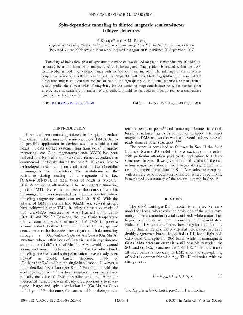
A typical trilayer structure�Ga,Mn�As/GaAs/AlAs/GaAs/ �Ga,Mn�As used in experi-ments is shown in Fig. 1. It consists of two �Ga,Mn�As lay-ers separated by a thin layer made of AlAs. Two additionallayers of GaAs are inserted to prevent diffusion of Mn intoAlAs. Since there are six channels possible for tunneling,i.e., mixing of different kinds of holes may happen depend-ing on the scattering potential �barrier�, the transmissions andreflection coefficients should be normalized to the groupvelocity17
P. KRSTAJIĆ AND F. M. PEETERS PHYSICAL REVIEW B 72, 125350 �2005�
125350-2
T�� = �AR�+
AL�+ �2vgr�
vgr�
. �10�
The quantities AR�+ and AL�
+ are amplitudes of the quantummechanical waves right and left of the structure, while � ,�denote various hole states. The conservation of the probabil-ity current leads to six relations among transmission and re-flection coefficients
��
�T�� + R��� = 1. �11�
Here the variable � assumes all six hole states �h1, h2, l1, l2,s1, and s2�. These relations are also useful to check the con-sistency of the numerical calculations. Formally present inEq. �11� split-off band states s1, s2 do not contribute to thecurrent since the band edge of the LH “upper subband” isstill higher than the SO down subband ��SO �ex�. Theyinfluence the current values, however, in an indirect waysince the imaginary parts of kso are small, and because the
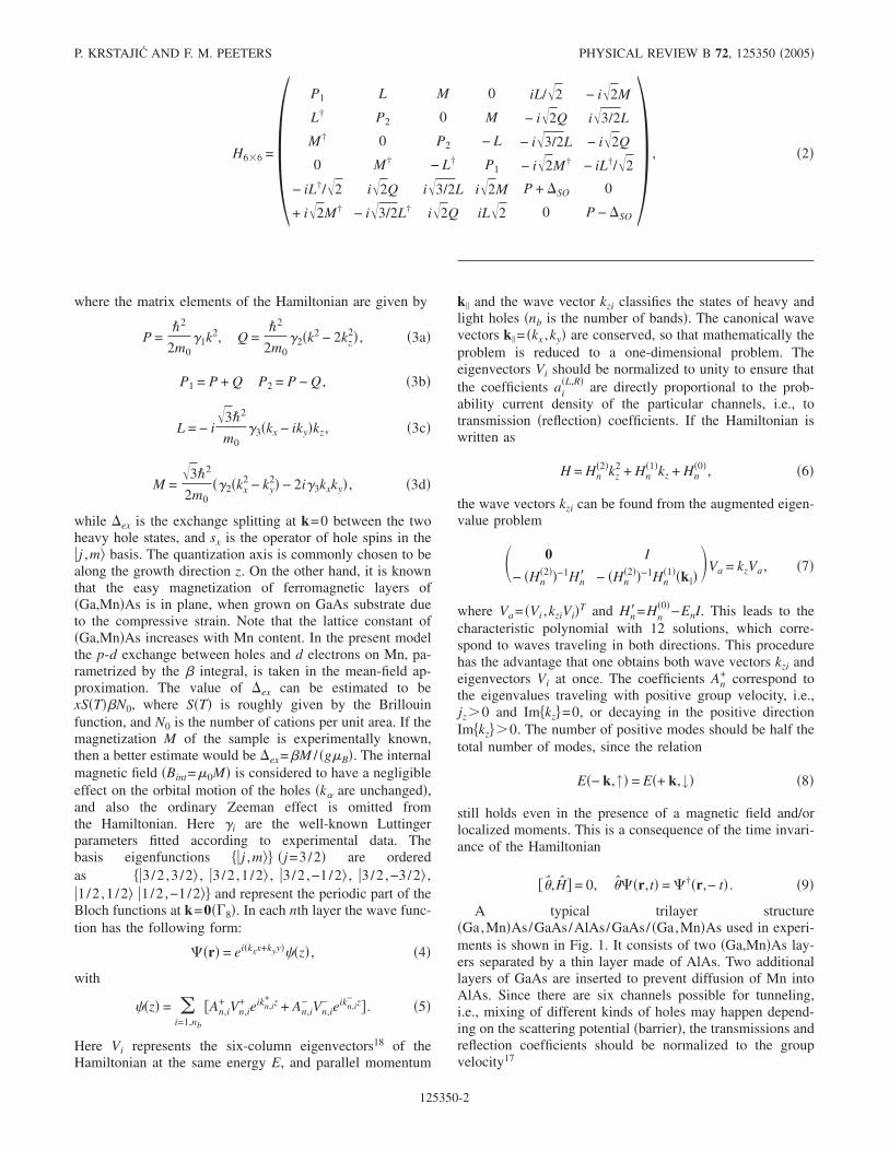
matrix component �2Q �that contains kz� mixes LH and SOholes. Thus, one should take into account more precisely thedispersion relation �hh,lh�k� obtained from H6�6 when �hh ap-proaches the SO band. A better insight into band alignmentof materials is given in Fig. 2, with GaAs spacers excluded.The scheme of dispersions E�kz� are given for kx=0, ky =0,for �Ga0.96 ,Mn0.04�As �first FM layer� and for pure AlAs and�Ga0.966 ,Mn0.034�As �second FM layer�. The valence band ofAlAs is shifted by 0.75 eV to the total barrier heightAlAs/GaAs and GaAs/ �Ga,Mn�As. The smaller splittingbetween the heavy holes as compared to the one of the lightholes is a result of spin-orbit interaction19,20 and the fact thatthe magnetization M is in plane.
III. RESULTS
The numerical method is based on the transfer matrixmethod for stratisfied media. The coefficients A on eitherside are connected by
�A+
0� = T�I�
r� , �12�
where the column I� contains 1 for the �th channel, the otherbeing zero, i.e., I�=�i�, while the r subcolumn contains re-
flection coefficients. The matrix M is composed of theboundary matching matrix Mi and the propagation matrix P,
T = MN−1�MN−1PNMN−1
−1 � ¯ �M1PM1−1�M0, �13�
whose explicit expressions can be found elsewhere.21 In thecase of a trilayer one has three layers GaAs/AlAs/GaAs,while two �thick� layers of �Ga,Mn�As act as the emitter andcollector leads. It is found22 that GaAs acts as a barrier to�Ga,Mn�As, whose height depends on the manganese con-tent. Its experimental value is in the range �88,146� meV forx�Mn� �1.2–2.5 % � according to Ref. 22 and consistent withRef. 7. Having found transmission coefficients T�� , � , �=1, . . . ,6 from Eq. �13�, the current density is given by
JC =e
8�3��
0
kt max
ktdkt�0
2�
d�����
T��� ,
in the limit of small Vbias��F. The tunneling current, Eq.�14�, is calculated for both alignment of the two �Ga,Mn�As,so that the tunneling magnetoresistance is found from
TMR =JCp − JCa
JCa, �14�
where JCp is the density of tunneling current when the twoFM films are parallel, while JCa denotes the current densitywhen the two are antiparallel. For our numerical calculationswe used the sample parameters of Ref. 5. These parametersare as follows: the width of two GaAs layers is D0=1 nm,the barrier thickness D of AlAs varied from1.2 nm to 2.2 nm, and the Mn molar contents of the twoDMS layers are 4.0% and 3.3%. The exchange energies cor-responding to these values are �ex
L =0.12 eV and �exR
=0.1 eV, respectively, assuming full alignment of manga-nese localized moments. The different manganese concentra-tion is made deliberately in order to build in the discrepancyin coercivity of the two DMS layers, i.e., to allow an easychange from parallel to antiparallel orientation. The appliedbias was eVbias=1 meV, much smaller than the Fermi level
FIG. 1. Schematic band diagram of a trilayer structure made oftwo DMS layers �Ga,Mn�As separated by an AlAs layer acting as abarrier. Two additional layers of GaAs are inserted in between inorder to prevent diffusion of Mn into the barrier.
FIG. 2. Scheme of band positions of the two �Ga,Mn�As layersand the barrier of AlAs. The band diagram of GaAs and split-offband of AlAs are not shown for clarity.
SPIN-DEPENDENT TUNNELING IN DILUTED… PHYSICAL REVIEW B 72, 125350 �2005�
125350-3
�F�80 meV. The barrier height Vb=0.75 eV and the mea-surement was performed at low temperature T=8 K, whichjustifies using Eq. �14�. The barrier height Vb2 between�Ga,Mn�As and GaAs is taken to be approximately 0.2 eV,since x�Mn� is higher than 3%. The Luttinger parameters are�1
�1�=6.85, �2�1�=2.1, �3
�1�=2.9 �GaAs�, and �1�2�=3.45, �2
�2�
=1.29, �3�2�=0.68 �AlAs�. In order to gain better insight in the
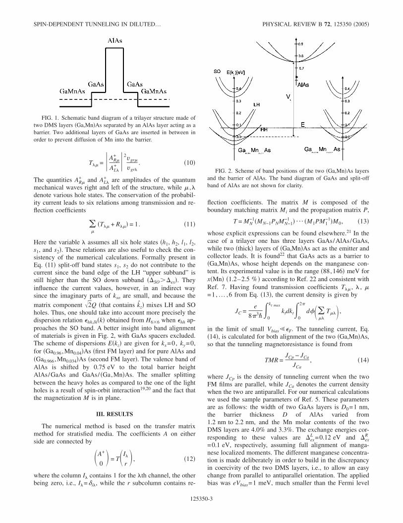
process of tunneling, we show the current density for thecase of parallel orientation of the two DMS layers �Fig. 3�and for antiparallel �Fig. 4� orientation. Out of the 36 pos-sible transmissions, only 12 are nonzero since the split-offband is below the Fermi energy, and within the barrier thereis no magnetic field. This means, for instance, that the trans-missions between HH1 and HH2, and between LH1 andLH2, are not possible because of the presence of zeros on thesmall off-diagonal in the matrix elements of Eq. �2�. How-ever, out of these 12 channels only about four to eight aresignificant depending on the alignment of the ferromagneticlayers. The current components, when the two FM are par-allel, are shown in Fig. 3. Only one component, light hole tolight hole, is significantly larger than the other as a result of
their lighter mass. They exhibit rapid decay with the barrierthickness. In the next figure, i.e., Fig. 4, we present the re-sults for the antiparallel case, where one can notice signifi-cantly smaller values for the tunnel currents. The closelyspaced curves, two by two, are a consequence of a differentMn content of the two FM layers, i.e., they have differentexchange splitting. Thus the transmission probabilities LH1into LH1 and LH2 into LH2 are not the same. On the otherhand, the different polarizations of heavy and light holes isbecause the HH eigenfunctions have a definite value of spin,
�3
2,3
2� =
1�2
�X + iY↑; �3
2,−
3
2� =
i�2
�X − iY↓ ,
�15�
while the LH eigenfunctions are composed of different spinsubspaces,
�3
2,1
2� =
i�6
��X + iY↓− 2�Z↑� , �16a�
�3
2,−
1
2� =
1�6
��X − iY↓ + 2�Z↓� . �16b�
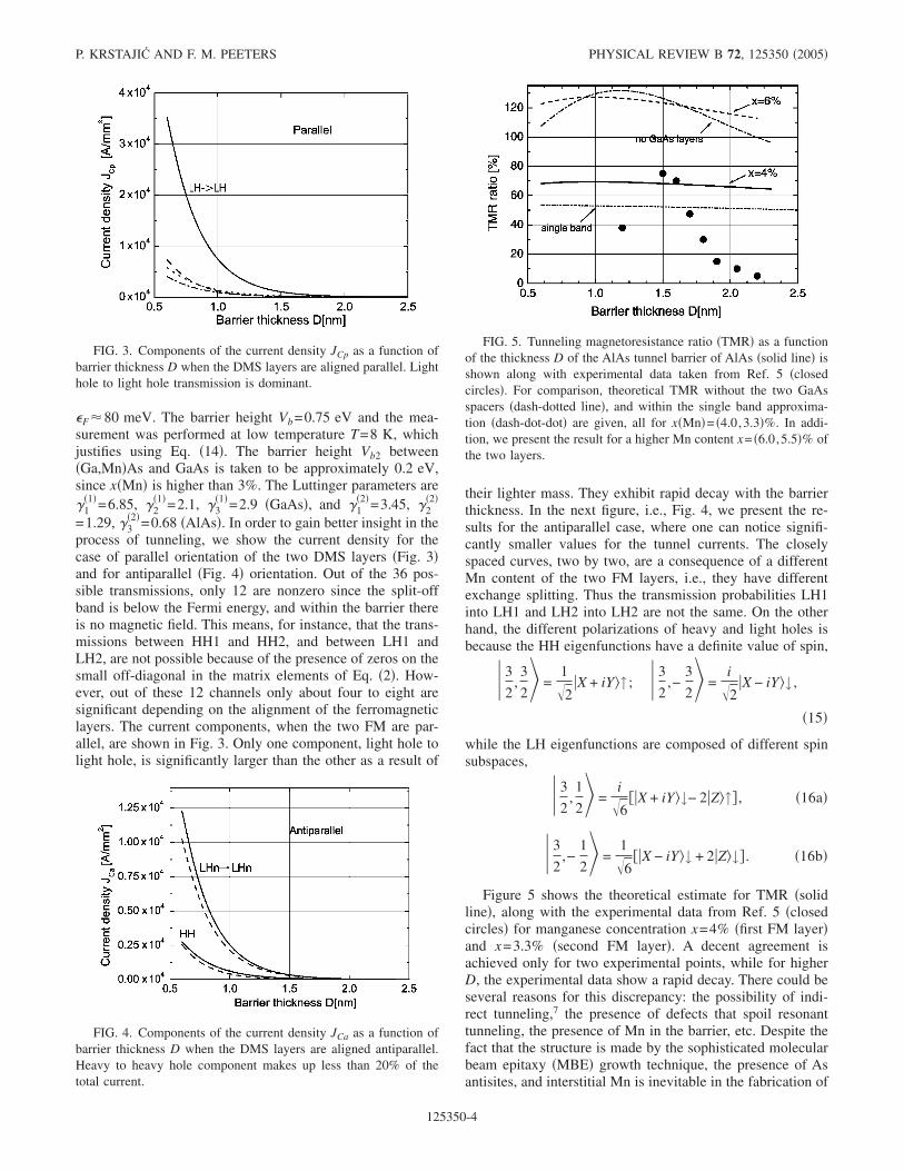
Figure 5 shows the theoretical estimate for TMR �solidline�, along with the experimental data from Ref. 5 �closedcircles� for manganese concentration x=4% �first FM layer�and x=3.3% �second FM layer�. A decent agreement isachieved only for two experimental points, while for higherD, the experimental data show a rapid decay. There could beseveral reasons for this discrepancy: the possibility of indi-rect tunneling,7 the presence of defects that spoil resonanttunneling, the presence of Mn in the barrier, etc. Despite thefact that the structure is made by the sophisticated molecularbeam epitaxy �MBE� growth technique, the presence of Asantisites, and interstitial Mn is inevitable in the fabrication of
FIG. 3. Components of the current density JCp as a function ofbarrier thickness D when the DMS layers are aligned parallel. Lighthole to light hole transmission is dominant.
FIG. 4. Components of the current density JCa as a function ofbarrier thickness D when the DMS layers are aligned antiparallel.Heavy to heavy hole component makes up less than 20% of thetotal current.
FIG. 5. Tunneling magnetoresistance ratio �TMR� as a functionof the thickness D of the AlAs tunnel barrier of AlAs �solid line� isshown along with experimental data taken from Ref. 5 �closedcircles�. For comparison, theoretical TMR without the two GaAsspacers �dash-dotted line�, and within the single band approxima-tion �dash-dot-dot� are given, all for x�Mn�= �4.0,3.3�%. In addi-tion, we present the result for a higher Mn content x= �6.0,5.5�% ofthe two layers.
P. KRSTAJIĆ AND F. M. PEETERS PHYSICAL REVIEW B 72, 125350 �2005�
125350-4
�Ga,Mn�As. Another reason is the presence of two GaAslayers on both sides, whose thickness is comparable with thewidth of the trilayer structure and is not changed in the ex-periment, while the barrier they impose is not so high. This isclearly shown on the same figure, where the dash-dotted linecorresponds to the TMR in the absence of the two GaAslayers. The slope of the curve is more pronounced than in theprevious case. On the other hand, the considered model doesnot have any fitting parameter, so that the semiquantitativeagreement is satisfactory. Clearly, in order to enhanceTMR, one should enlarge the spin-splitting of the holes in�Ga,Mn�As, e.g., by increasing the Mn content. Calculationsof TMR for x=6% �x=5.5% � are given in the same Fig. 5�dashed line�. The predicted value of the magnetoresistancefor this x�Mn� reaches 130%, a promising value, but it wasobtained under the assumption that there are no self-compensation effects, either for the hole density or the mag-netization of the layers.
IV. SINGLE BAND APPROXIMATION
In order to gain better insight into the tunneling processes,we depart from the 6�6 Luttinger-Kohn model and analyzethe problem within the single band approximation. Thisserves only as an illustration and to explain qualitatively theslow variation of the TMR ratio on the barrier thickness. Thewave function in the three regions, for an incoming spin-upstate is
�I�z � 0� = V↑eikz↑z + r↑↑V↑e
−ikz↑z + r↑↓V↓e−ikz↓z, �17a�
�II�0 � z � d� = A↑V↑eikz2↑z + B↑V↑e
−ikz2↑z + A↓V↓eikz2↑z
+ B↓V↓e−ikz2↓z, �17b�
�III�z � d� = t↑↑V↑eikz↑z + t↑↓V↓e
ikz↓z, �17c�
where
V↑ =1�2
�1
1�, V↓ =
1�2
� 1
− 1� . �18�
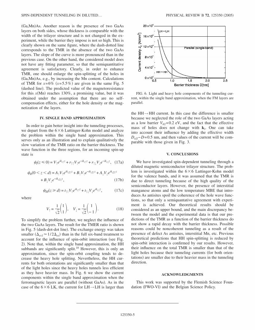
To simplify the problem further, we neglect the influence ofthe two GaAs layers. The result for the TMER ratio is shownin Fig. 5 �dash-dot-dot line�. The exchange energy was takensmaller ��ex1�1/2�ex� than in the full six-band treatment toaccount for the influence of spin-orbit interaction �see Fig.2�. Note that, within the single band approximation, the HHsubbands are significantly split.10 However, this is only anapproximation, since the spin-orbit coupling tends to de-crease the heavy hole splitting. Nevertheless, the HH cur-rents for both orientations are significantly smaller than thatof the light holes since the heavy holes tunnels less efficientas they have heavier mass. In Fig. 6 we show the currentcomponents within the single band approximation when theferromagnetic layers are parallel �without GaAs�. As in thecase of the 6�6 LK, the current for LH→LH is larger than
the HH→HH current. In this case the difference is smallerbecause we neglected the role of the two GaAs layers actingas a low barrier Vb2=0.2 eV, and the fact that the effectivemass of holes does not change with k . One can takeinto account their influence by adding the effective widthDef f −D=0.5 nm, and then values of the current will be com-parable with those given in Fig. 3.
V. CONCLUSIONS
We have investigated spin-dependent tunneling through adiluted magnetic semiconductor trilayer structure. The prob-lem is investigated within the 6�6 Luttinger-Kohn modelfor the valence bands, and it was assumed that the TMR isdue to direct tunneling because of the high quality of thesemiconductor layers. However, the presence of interstitialmanganese atoms and the low temperature MBE that intro-duces As antisites spoil the coherence of the hole wave func-tions, so that only a semiquantative agreement with experi-ment is achieved. Our theoretical results should beconsidered as an upper bound, and the main discrepancy be-tween the model and the experimental data is that our pre-dictions of the TMR as a function of the barrier thickness donot show a rapid decay with the barrier thickness. Possiblereasons could be noncoherent tunneling as a result of thepresence of defect As antisites, interstitial Mn, etc. Previoustheoretical predictions that HH spin-splitting is reduced byspin-orbit interaction is confirmed by our results. However,their influence on the total TMR is smaller than that of thelight holes because their tunneling currents �for both orien-tations� are smaller due to their heavier mass in the tunnelingdirection.
ACKNOWLEDGMENTS
This work was supported by the Flemish Science Foun-dation �FWO-Vl� and the Belgian Science Policy.
FIG. 6. Light and heavy hole components of the tunneling cur-rent, within the single band approximation, when the FM layers areparallel.
SPIN-DEPENDENT TUNNELING IN DILUTED… PHYSICAL REVIEW B 72, 125350 �2005�
125350-5
*Electronic address: [email protected]†Electronic address: [email protected] S. A. Wolf, D. D. Awschalom, R. A. Buhrman, J. M. Daughton,
S. von Molnar, M. L. Roukes, A. Y. Chtchelkanova, and D. M.Treger, Science 294, 1488 �2001�.
2 S. Datta and B. Das, Appl. Phys. Lett. 56, 665 �1990�.3 T. Dietl, Semicond. Sci. Technol. 17, 377 �2002�.4 D. Chiba, F. Matsukura, and H. Ohno, Physica E �Amsterdam�
21, 966 �2004�.5 M. Tanaka and Y. Higo, Phys. Rev. Lett. 87, 026602 �2001�.6 Y. Higo, H. Shimizu, and M. Tanaka, J. Appl. Phys. 89, 6745
�2001�.7 R. Mattana, M. Elsen, J.-M. George, H. Jaffrès, F. N. Van Dau, A.
Fert, M. F. Wyczisk, J. Olivier, P. Galtier, B. Lépine, A.Guivarc’h, and G. Jézéquel, Phys. Rev. B 71, 075206 �2005�.
8 S. S. Makler, M. A. Boselli, J. Weberszpil, X. F. Wanga, and I. C.da Cunha Lima, Physica B 320, 396 �2002�; S. S. Makler, M. A.Boselli, J. Weberszpil, X. F. Wanga, and I. C. da Cunha Lima,ibid. 354, 348 �2004�.
9 J. M. Luttinger and W. Kohn, Phys. Rev. 97, 869 �1955�.10 A. G. Petukhov, A. N. Chantis, and D. O. Demchenko, Phys. Rev.
Lett. 89, 107205 �2002�.11 A. G. Petukhov, D. O. Demchenko, and A. N. Chantis, Phys. Rev.
B 68, 125332 �2003�.12 T. Dietl, H. Ohno, and F. Matsukura, Phys. Rev. B 63, 195205
�2001�.13 S. C. P. Rodrigues, L. M. R. Scolfaro, J. R. Leite, I. C. da Cunha
Lima, G. M. Sipahi, and M. A. Boselli, Phys. Rev. B 70, 165308�2004�.
14 R. Wessel and M. Altarelli, Phys. Rev. B 39, 12802 �1989�.15 E. T. Yu, M. K. Jackson, and T. C. McGill, Appl. Phys. Lett. 55,
744 �1989�.16 N. Malkova and U. Ekenberg, Phys. Rev. B 66, 155324 �2002�.17 P. Krstajić and F. M. Peeters, Phys. Rev. B 71, 115321 �2005�.18 L. C. Andreani, A. Pasquarello, and F. Bassani, Phys. Rev. B 36,
5887 �1987�.19 T. Dietl, A. Haury, and Y. M. d’Aubigne, Phys. Rev. B 55, R3347
�1997�.20 T. Dietl, J. Phys.: Condens. Matter 16, S5471 �2004�.21 C. Y. Chao and S. L. Chuang, Phys. Rev. B 43, 7027 �1991�.22 Y. Ohno, I. Arata, F. Matsukura, and H. Ohno, Physica E
�Amsterdam� 13, 521 �2002�.
P. KRSTAJIĆ AND F. M. PEETERS PHYSICAL REVIEW B 72, 125350 �2005�
125350-6