spin-dependent delay time in electronic resonant tunneling at zero magnetic field
TRANSCRIPT
Spin-dependent delay time in electronic resonant tunneling at zeromagnetic field
O. Voskoboynikova,b,* , S.S. Liua, C.P. Leea
aNational Chiao Tung University, 1001 Ta Hsueh Road, Hsinchu 30010, Taiwan, ROCbKiev Taras Shevchenko University, 64 Volodymirska st., 252030 Kiev, Ukraine
Received 24 January 2000; accepted 21 May 2000 by S. Ushioda
Abstract
The dependence of the phase tunneling time on electronic spin polarization in symmetric and asymmetric double-barriersemiconductor heterostructures is studied theoretically. The effective one-band Hamiltonian approximation and spin-dependentboundary conditions are used for theoretical investigation of the electron spin influence on the delay time in tunnelingprocesses. It is shown that the spin–orbit splitting in the dispersion relation for the electrons can provide a dependence ofthe delay time on the electron spin polarization without additional magnetic field. This dependence can be controlled by anexternal electric field and can be very pronounced for realistic double-barrier semiconductor heterostructures.q 2000 ElsevierScience Ltd. All rights reserved.
Keywords:A. Quantum wells; A. Semiconductors; D. Spin–orbit effects; D. Tunneling
An understanding of the time aspects of tunnelingprocesses is of much significance [1–3]. Apart from atheoretical interest [1,3], this understanding is of importancebecause of increasing attention on miniaturizing tunnelsemiconductor devices [4]. Although in recent years thetunneling time of an electron through double-barrier reso-nant heterostructures (DBRH) has been studied extensively,the concept of the tunneling time is still not as clear as it isdesired [1]. In fact, tunneling time is a basic characteristicthat determines the dynamic range of tunneling devices.There are several quantities used in description of thetunneling process with the dimensions of time. These timecharacteristics have been introduced by different authors todescribe different aspects of electron dynamics [5–9].Additional complexity arises with some recent publicationsthat demonstrated position-dependent effective mass andparallel (to interfaces) motion dependence of the tunnelingprocess [10–16]. Since the miniature tunnel semiconductordevices typically have position-dependent effective electronmass, the parallel (in-plane) motion of the electron canprovide additional specific effects [15,16].
In this article we call attention to another consequence forthe tunneling time theory that originates from the electronparallel motion in DBRH. It is well known that there is aspin–orbit coupling between in-plane electron motion andthe electron spin polarization [17–20]. The coupling causesspin-splitting in the electronic energy band in asymmetricheterostructures or heterostructures with an external electricfield [21–24]. Recently, it has been found that this effect isalso strong in tunnel barrier structures and can lead to spin-dependent tunnel coefficients [25–27]. There are two contri-butions to the spin-splitting effect that can be distinguished,which play different roles: band-edge discontinuity at thestructure interfaces and additional electrostatic potential.The former brings about the spin-dependent boundaryconditions to the tunnel problem and the latter gives aspin-dependent term in the effective mass Hamiltonian[21–24]. Both of them form different tunneling resonanceconditions for different spin polarizations of tunneling elec-trons and lead to a spin-splitting of the resonance level in theasymmetric DBRH well [26,27]. The spin-split levels corre-spond to different electronic spin polarizations andobviously have different characteristic times of the electrontunnel process. We will show below that the spin–orbitcoupling can lead to significant differences in tunneling
Solid State Communications 115 (2000) 477–481
0038-1098/00/$ - see front matterq 2000 Elsevier Science Ltd. All rights reserved.PII: S0038-1098(00)00221-0
PERGAMONwww.elsevier.com/locate/ssc
* Corresponding author. Tel.:1886-3-571-2121; fax:1886-3-572-4361.
E-mail address:[email protected] (O. Voskoboynikov).
times for different electron spin polarizations at zeromagnetic field.
In this investigation we use the “stationary phaseapproach” to the tunneling time definition introduced byBohm [5]. It is a well-understood and widely used definitionthat actually deals with the phase delay time. The delay timecan be described as the energy derivative of the phaseQ ofthe structure transmission amplitude
t � "2Q
2Ez; �1�
where Ez denotes the longitudinal (corresponding to amotion along the perpendicular direction to the heterostruc-ture interface) component of the electron’s total energy.
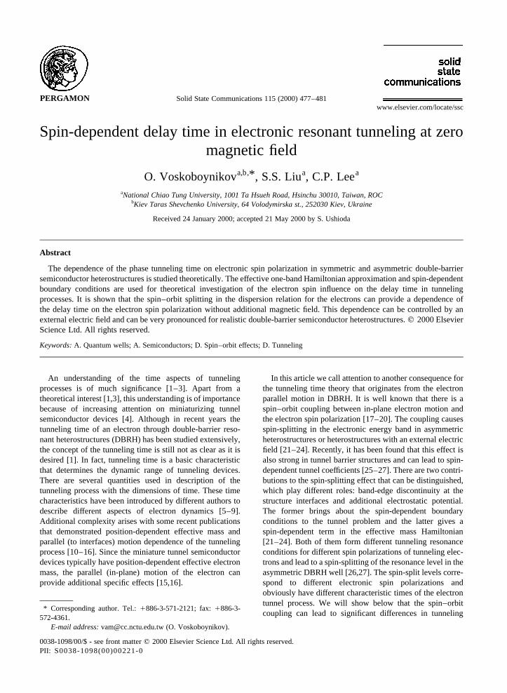
We describe here a DBRH with variations of the bandstructure parameters with an external electric field, as shownin Fig. 1. Layers of the structure are perpendicular to thez-axis, the in-plane electron’s wave vector isk (if k is putalong an arbitraryx direction, the spin polarization is setalong they-axis in the layer plane). In the structure wehave two sources for thek-vector dependence of the trans-mission coefficient: through position-dependent energyband parameters (as in Refs. [10–15]), and through thecoupling between in-plane electron motion and the elec-tron’s spin polarization produced by the external electricfield. The last one can lead to the spin polarization depen-dence in symmetric DBRH (sDBRH). The former leads tothe spin-dependent boundary conditions and manifests thespin-splitting effect when the DBRH is asymmetric(aDBRH), even without an additional electric field[23,26,27]. We use the effective quasi-one-dimensionalone-electronic-zone Hamiltonian [23] within the envelope
function approximation for the total wave function of theelectronFs (z, r ) and can present the function as
F js�z; r� � C js�z� exp�ik·r�;whereC js�z� satisfies thez-component of the Schro¨dingerequation in thejth region ands � ^1 refers to the spinpolarization. The mass and spin-dependent boundary condi-tions forC js�z� at an interface planez� zj betweenj andj 1 1 regions have been introduced in Ref. [23]
1mj�E�
ddz
ln�C js�z��� �
z�zj
21
mj11�E�ddz
ln�C j11s�z��� �
z�zj
� 2sk�b j11�E�2 bj�E��"2 ;
C js�zj�2 C j11s�zj� � 0;
�2�where
1m�E; z� �
P2
"2
�2
E 2 Ec�z�1 Eg�z�1 V�z�
11
E 2 Ec�z�1 Eg�z�1 D�z�1 V�z��
�3�
is position- and energy-dependent electronic effective massin nonparabolic approximation and
b�E; z� � P2
2
�1
E 2 Ec�z�1 Eg�z�1 V�z�
21
E 2 Ec�z�1 Eg�z�1 D�z�1 V�z��
�4�
is position- and energy-dependent electronic spin-couplingparameters. In Eqs. (2) and (3),E denotes the total electronenergy in the conduction band,V�z� � 2eFzis the externalelectric potential (F—the electric field,e—the electron’scharge). The matrix elementP is assumed to bez-indepen-dent [28];Ec�z�; Eg�z�; andD�z� stand correspondingly forz-dependencies of the conduction-band-edge, the main bandgap, and the spin–orbit splitting profiles.
The most attractive material system for the spin-splittingeffects in DBRH preferably should contain a component ofnarrow-band semiconductors [17,18,21]. It worth noticingthat the parabolic approximation in the electron motiondescription can lead to incorrect results for this case[22,25]. Therefore, in our calculations we use valuesbelow the nonparabolic approximation (2) for the electronicdispersion relations in all materials of the structures.
To obtain the structure tunneling transmission amplitude,we use the transfer matrix method [29] with the boundaryconditions above Eq. (2) as was described in Ref. [26]. Thepotential profile in the DBRH consists of five regions and thetotal transfer matrix, which matches regions 5 and 1, can bewritten as
Ms �4j�1 M j
s �5�
O. Voskoboynikov et al. / Solid State Communications 115 (2000) 477–481478
Fig. 1. Variation of the semiconductor-band parameters in DBRHwith external electric field.

In Eq. (4)M js is the transfer matrix that matches regionsj
and j 1 1: The structure transmission amplitude is equal to�Ms11�21 and we can finally write
ts�Ez; k� � 2"2 arg�Ms11�
2Ez; �6�
which is the equation we use to calculate the spin-dependentdelay time of the double-barrier structures.
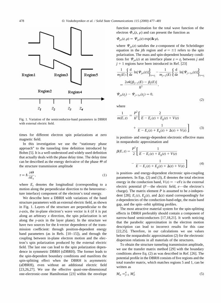
The delay time is a function of the two variablesEz andk.The function normally demonstrates a sharp peak for onedefined polarization of the electron spin [8]. Consequently,
in the Ez–k plane we have two overlapping peaks for twopolarizations [26,27]. From the point of view of possibleapplications, it is interesting to clarify a difference betweenthe tunneling times for electrons with identical energy andwave vectors and different spin polarizations. Because thepeaks have very sharp dependencies in theEz–k plane[8,26,27], to get a quantitative filling about possibledifference of the delay time for electrons with differentspin polarizations, it is useful to calculate and present alogarithmic ratio of the times with spin-up�t"� andspin-down�t#� polarization
T�Ez; k� � log10t"t#
�7�
First, we consider an sDBRH composed of two identicalInAs–GaAs–InAs barriers (parameters of materials arefrom Refs. [28,30]). The thickness of the GaAs barriers ischosen asz2 2 z1 � z5 2 z4 � 30 �A; and InAs well width isz2 2 z3 � 60 �A: For this structure, the spin-splitting effect inthe tunneling processes comes only when we apply theexternal electric field. The three-dimensional plot ofT�Ez; k� in Fig. 2(a) presents two sharp peaks, one positiveand one negative (corresponding to the spin-split resonancelevels [26,27]), where the tunneling delay time is stronglydependent on the spin polarization. The difference increaseswith increase of thek vector and the external electric fieldmagnitude. This is demonstrated in Fig. 2(b). Curvesa–c inFig. 2(b) correspond to different values of the external elec-tric field, whenk � 4 × 106 cm21
: Absolute values of thetime for the described sDBRH lie between 10212 and10215 s. It should be noticed that the ratio between thedelay times can gain a few orders in magnitude.
The delay time (near resonance energy in theEz–k plane)presents the halfwidth of the resonance peak for the tunnel-ing probabilityGs < 2"=ts�Es
z �k��; Esz �k� is the resonance
peak position inEz–kplane [8]. Our results show that condi-tions of the electrons “trapped” in resonant two-dimensionalstates inside the well can depend strongly on the electronspin polarization. The decay time of the states (or the timespent by an electron in the well) becomes also different forthe electrons with different spin polarizations. We cancontrol the difference by the external electric field. Thesefacts could be a base for experimental investigations andpractical applications of the effect.
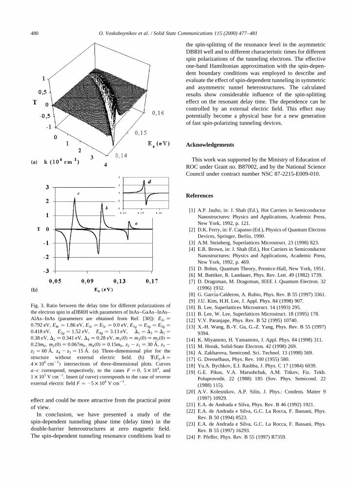
In Fig. 3(a), we have shown results of theT�Ez; k� calcu-lation for an aDBRH with electronic-band parameters ofInAs–GaAs–InAs–AlAs–InAs [30]. The thicknesses ofGaAs and AlAs barriers are 35 and 15 A˚ , respectively,and InAs well width is 60 A˚ . For this structure we have abig polarization effect even without any external electricfield. The effect is originated from the built-in asymmetryof the structure [22,23]. Additional external electric fieldcan increase, suppress, and even reverse the effect asshown in Fig. 3(b). Curved in the insert to Fig. 3(b) demon-strates the last situation. We can conclude that involving theaDBRH extends the range of opportunities to control the
O. Voskoboynikov et al. / Solid State Communications 115 (2000) 477–481 479
Fig. 2. Ratio between the delay time for different polarization of theelectron spin in sDBRH with parameters of InAs–GaAs–InAs–GaAs–InAs (parameters are obtained from Ref. [30]):E2c � E4c �0:792 eV; E3c � E5c � 0:0 eV; E1g � E3g � E5g � 0:418 eV;E2g � E4g � 1:52 eV; D1 � D3 � D5 � 0:38 eV; D2 � D4 �0:341 eV; m1�0� � m3�0� � m5�0� � 0:023m0; m2�0� � m4�0� �0:067m0 (m0—the free electron’s mass),z2 2 z1 � z5 2 z4 �30 �A; z3 2 z2 � 60 �A: (a) T plot in Ez–k plane for external electricfield F � 5 × 10⁴ V cm21; (b) T�Ez; k � 4 × 106 cm21� inter-sections of the three-dimensional plots. Curvesa–c correspond,respectively, to the casesF � 2 × 10⁴
; 5 × 10⁴, and 1× 10⁵ V cm21.
effect and could be more attractive from the practical pointof view.
In conclusion, we have presented a study of thespin-dependent tunneling phase time (delay time) in thedouble-barrier heterostructures at zero magnetic field.The spin-dependent tunneling resonance conditions lead to
the spin-splitting of the resonance level in the asymmetricDBRH well and to different characteristic times for differentspin polarizations of the tunneling electrons. The effectiveone-band Hamiltonian approximation with the spin-depen-dent boundary conditions was employed to describe andevaluate the effect of spin-dependent tunneling in symmetricand asymmetric tunnel heterostructures. The calculatedresults show considerable influence of the spin-splittingeffect on the resonant delay time. The dependence can becontrolled by an external electric field. This effect maypotentially become a physical base for a new generationof fast spin-polarizing tunneling devices.
Acknowledgements
This work was supported by the Ministry of Education ofROC under Grant no. B87002, and by the National ScienceCouncil under contract number NSC 87-2215-E009-010.
References
[1] A.P. Jauho, in: J. Shah (Ed.), Hot Carriers in SemiconductorNanostructures: Physics and Applications, Academic Press,New York, 1992, p. 121.
[2] D.K. Ferry, in: F. Capasso (Ed.), Physics of Quantum ElectronDevices, Springer, Berlin, 1990.
[3] A.M. Steinberg, Superlattices Microstruct. 23 (1998) 823.[4] E.R. Brown, in: J. Shah (Ed.), Hot Carriers in Semiconductor
Nanostructures: Physics and Applications, Academic Press,New York, 1992, p. 469.
[5] D. Bohm, Quantum Theory, Prentice-Hall, New York, 1951.[6] M. Buttiker, R. Landauer, Phys. Rev. Lett. 49 (1982) 1739.[7] D. Dragoman, M. Dragoman, IEEE J. Quantum Electron. 32
(1996) 1932.[8] G. Garcia-Calderon, A. Rubio, Phys. Rev. B 55 (1997) 3361.[9] J.U. Kim, H.H. Lee, J. Appl. Phys. 84 (1998) 907.
[10] B. Lee, Superlattices Microstruct. 14 (1993) 295.[11] B. Lee, W. Lee, Superlattices Microstruct. 18 (1995) 178.[12] V.V. Paranjape, Phys. Rev. B 52 (1995) 10740.[13] X.-H. Wang, B.-Y. Gu, G.-Z. Yang, Phys. Rev. B 55 (1997)
9394.[14] K. Miyamoto, H. Yamamoto, J. Appl. Phys. 84 (1998) 311.[15] M. Horak, Solid-State Electron. 42 (1998) 269.[16] A. Zakharova, Semicond. Sci. Technol. 13 (1998) 569.[17] G. Dresselhaus, Phys. Rev. 100 (1955) 580.[18] Yu.A. Bychkov, E.I. Rashba, J. Phys. C 17 (1984) 6039.[19] G.E. Pikus, V.A. Marushchak, A.M. Titkov, Fiz. Tekh.
Poluprovodn. 22 (1988) 185 (Sov. Phys. Semicond. 22(1988) 115).
[20] A.V. Kolesnikov, A.P. Silin, J. Phys.: Condens. Matter 9(1997) 10929.
[21] E.A. de Andrada e Silva, Phys. Rev. B 46 (1992) 1921.[22] E.A. de Andrada e Silva, G.C. La Rocca, F. Bassani, Phys.
Rev. B 50 (1994) 8523.[23] E.A. de Andrada e Silva, G.C. La Rocca, F. Bassani, Phys.
Rev. B 55 (1997) 16293.[24] P. Pfeffer, Phys. Rev. B 55 (1997) R7359.
O. Voskoboynikov et al. / Solid State Communications 115 (2000) 477–481480
Fig. 3. Ratio between the delay time for different polarizations ofthe electron spin in aDBRH with parameters of InAs–GaAs–InAs–AlAs–InAs (parameters are obtained from Ref. [30]):E2c �0:792 eV; E4c � 1:86 eV; E3c � E5c � 0:0 eV; E1g � E3g � E5g �0:418 eV; E2g � 1:52 eV; E4g � 3:13 eV; D1 � D3 � D5 �0:38 eV; D2 � 0:341 eV; D4 � 0:28 eV; m1�0� � m3�0� � m5�0� �0:23m0; m2�0� � 0:067m0; m4�0� � 0:15m0; z2 2 z1 � 30 �A; z3 2
z2 � 60 �A; z4 2 z3 � 15 �A: (a) Three-dimensional plot for thestructure without external electric field. (b)T�Ez; k �4 × 106 cm21� intersections of three-dimensional plots. Curvesa–c correspond, respectively, to the casesF � 0; 5 × 10⁴, and1 × 105 V cm21. Insert (d curve) corresponds to the case of reverseexternal electric fieldF � 25 × 104 V cm21
:

[25] A. Voskoboynikov, S.S. Liu, C.P. Lee, Phys. Rev. B 58 (1998)15397.
[26] A. Voskoboynikov, S.S. Liu, C.P. Lee, Phys. Rev. B 59 (1999)12514.
[27] E.A. de Andrada e Silva, G.C. La Rocca, Phys. Rev. B 59(1999) R15583.
[28] G. Bastard, Wave Mechanics Applied to SemiconductorHeterostructures, Les Edition de Physique, Les Ulis, 1990.
[29] E.O. Kane, Tunneling Phenomenon in Solids, Plenum Press,New York, 1969.
[30] S.G. Shen, X.Q. Fan, J. Phys.: Condens Matter 9 (1997) 3151.
O. Voskoboynikov et al. / Solid State Communications 115 (2000) 477–481 481