spectral assignments in the infrared absorption region...
TRANSCRIPT

This journal is© the Owner Societies 2016 Phys. Chem. Chem. Phys., 2016, 18, 6239--6246 | 6239
Cite this:Phys.Chem.Chem.Phys.,
2016, 18, 6239
Spectral assignments in the infrared absorptionregion and anomalous thermal hysteresis in theinterband electronic transition of vanadiumdioxide films
Peng Zhang,a Mengjiao Li,a Qinglin Deng,a Jinzhong Zhang,a Jiada Wu,b
Zhigao Hu*a and Junhao Chua
The metal–insulator transition (MIT) is of key importance for understanding the fundamental electronic
interaction that determines the physical properties of vanadium dioxide (VO2) film. Here, the spectral
slopes of transmittance and reflectance in the infrared absorption region (about 0.62–1.63 eV) and the
interband electronic transitions for VO2 films with thicknesses of 27, 40 and 63 nm have been investigated.
The potential applications of the spectral slopes were presented in detail. It is found that the variation
of resistivity and transmittance increases with the spectral slopes of transmittance and reflectance. It is
surprising that the resistivity of the VO2 film with a thickness of 27 nm is larger than that of the VO2 film
with a thickness of 40 nm in the metal state. In addition, an anomalous counterclockwise thermal hysteresis
with higher energy from the interband electronic transition was also found during the MIT process for the
thinnest film. It is believed that this remarkable phenomenon could be related to the correlation effects in
the rutile phase, which could lead to the splitting of the a1g band into Hubbard bands. The lower Hubbard
band would result in an electronic transition blue-shift with the empty esg band, which can explain the origin
of the counterclockwise thermal hysteresis and the abnormal resistivity in the metal state.
1 Introduction
Vanadium dioxide (VO2) is a paradigmatic example of a prototypecorrelated electron system that is vital for both fundamentalphysics and applications. It is generally known that the VO2 showsan unusual first-order metal–insulator transition (MIT) aroundroom temperature with a variation in electrical conductivity ofseveral orders of magnitude.1,2 Furthermore, a change of latticestructure from a high temperature, rutile (P42/mn) to a lowtemperature, monoclinic (P21/c) has been observed during theMIT process.3,4 Several models have been proposed to accountfor the origin of the MIT process. The mechanism of the MIT canbe electronically (Mott transition), structurally (Peierls transition)or collaboratively (Mott–Peierls transition) driven, and is usuallyassociated with the electronic ordering phenomenon.5–7 Becauseof the complicated relationship between the electron–latticecoupling and the electron–electron interactions, the origin of
and the fundamental mechanism driving the transition are stillcontroversial.
Due to its prominent optical and electrical properties, VO2 is apromising candidate for a variety of applications, such as in sensordevices, modulators, and optical and electrical switching.8–10,12
The MIT properties could be manipulated using not onlytemperature, but also electric fields, strain, doping and pressureetc.13–16 In the past several decades, the impact of the abovefactors on the internal mechanism of MIT has been studiedwidely. A lot of interesting and new phenomena were foundthrough various kinds of measurement techniques. However, theeffect of the thickness on the energy transition was often ignoredand scarcely investigated. It is well known that the dynamics ofthe electronic correlations may substantially differ from theconventional physics when the film thickness is relatively thin.The interband transitions can be affected by altering the filmthickness, which has important implications in a correlatedsystem with Coulomb repulsion between electrons and orbitaloverlaps. Therefore, it is necessary to provide additional insightinto the underlying mechanism of the energy transition for thecases of films with different thicknesses.
In this study, the VO2 films with different thicknesses wereprepared using pulsed laser deposition (PLD). The spectral slopesof transmittance and reflectance in the infrared absorption region
a Key Laboratory of Polar Materials and Devices, Ministry of Education,
Department of Electronic Engineering, East China Normal University,
Shanghai 200241, China. E-mail: [email protected]; Fax: +86-21-54345119;
Tel: +86-21-54345150b Department of Optical Science and Engineering, Fudan University,
Shanghai 200433, China
Received 2nd December 2015,Accepted 28th January 2016
DOI: 10.1039/c5cp07416a
www.rsc.org/pccp
PCCP
PAPER
Publ
ishe
d on
28
Janu
ary
2016
. Dow
nloa
ded
by E
ast C
hina
Nor
mal
Uni
vers
ity o
n 22
/02/
2016
02:
31:3
0.
View Article OnlineView Journal | View Issue

6240 | Phys. Chem. Chem. Phys., 2016, 18, 6239--6246 This journal is© the Owner Societies 2016
were elucidated in detail. It is found that the resistivity in themetal state does not decrease with the film thickness, whichcan be ascribed to the variation of the carrier concentration. Inaddition, an anomalous counterclockwise thermal hysteresisbehavior in a higher energy transition was found for thethinnest VO2 film. It is believed that the remarkable phenomenoncould be related to the correlation effects in the rutile phase, whichis the origin of the abnormal resistivity and counterclockwisethermal hysteresis behavior.
2 Experimental details2.1 Fabrication, microstructure, optical and electricalcharacterization of VO2 films
The films were synthesized using a pulsed laser deposition (PLD)technique and the systematic study of the growth conditions canbe found elsewhere.17 Atomic force microscopy (AFM: DigitalInstruments Icon, Bruker) was used to characterize the surfacemorphology of the VO2 films. To evaluate the thickness andobserve the surface microstructure of the VO2 films, scanningelectron microscopy (SEM: Philips XL30FEG) was performed.X-ray diffraction (XRD) with Cu Ka radiation (l = 0.1542 nm) wasused to characterize the crystal structure of the films. To analyzethe electrical properties, the resistance as a function of thetemperature with different thicknesses was measured using aTHMSE 600 heating/cooling stage (Linkam Scientific Instruments)in a temperature range from 273 to 373 K. In order to determine thecomponents and valence states, X-ray photoelectron spectroscopy(XPS, AXIS UltraDLD, Japan) with Al Ka radiation (hn = 1486.6 eV)was carried out at room temperature under vacuum. Thetemperature-dependent transmittance spectra and near-normal inci-dent (about 81) reflectance spectra were recorded using a doublebeam ultraviolet-infrared spectrophotometer (PerkinElmer Lambda950) at a photon energy from 0.46 to 6.52 eV (190–2650 nm).
3 Results and discussion3.1 Microstructure analysis
Atomic force microscopy (AFM) images of the films are shownin Fig. 1(a)–(c). It can be seen that the VO2 films include manyindividual grains and the size of the nanoparticles increaseswith the film thickness. Fig. 1(d)–(f) show the high resolutionscanning electron microscopy (SEM) pictures of the VO2 films,which reveal that the samples consist of homogeneous andcontinuous nanoparticles. It can be found that the size of thegrains also increases gradually with the film thickness, which isconsistent with the AFM results. From the cross section shapesin Fig. 1(g)–(i), the film thickness is about 27, 40 and 63 nm.Fig. 2(a) shows the XRD diffraction patterns in a regular y–2yscanning mode for the VO2 films with different thicknesses.The peaks located at 2y = 27.921 correspond to the (011) planefor the VO2 films. It is found that the position of the (011) peakis nearly the same for each film thickness, which demonstratesthat the strain is almost relaxed between the interface of thefilm and substrate. This can also be reflected by the TMIT
extracted from the differential hysteresis loops of the resistivityand transmittance. The full width at half maximum of the (011)peaks decreases with the film thickness, which illustrates thatthe crystal quality can be improved with the film thickness.
3.2 Electrical transport
The resistivity change during a heating–cooling cycle across thetransition regime is shown in Fig. 2(b). The inset presents thedifferential curves of the resistivity hysteresis loops. In order toanalyze and compare the transport behavior of the VO2 films,the parameters of the electrical properties have been extractedfrom the related differential curves fitted using a Gaussianfunction, wherein Tc represents the phase transition tempera-ture. The discrepancy of the Tc between the heating and coolingprocess was defined as DTc. The phase transition magnitudeand the resistivity at the metal state was denoted as DA and Rr,respectively. The parameters are presented in Table 1. It can beseen that the variation of the resistivity for the VO2 films withthicknesses of 27, 40 and 63 nm is 133, 175 and 875, whichincreases with the film thickness. It is worth noting that the
Fig. 1 (a–c) AFM images of the VO2 films with thicknesses of 27, 40 and63 nm. (d–f) The high resolution SEM pictures of the VO2 films withdifferent thicknesses. (g–i) The cross section shapes of the films.
Fig. 2 (a) The y–2y scan XRD curves for thickness dependent VO2 films.(b) The resistivity as a function of temperature for the VO2 films withdifferent thicknesses. The inset shows differential curves of the resistivity.
Paper PCCP
Publ
ishe
d on
28
Janu
ary
2016
. Dow
nloa
ded
by E
ast C
hina
Nor
mal
Uni
vers
ity o
n 22
/02/
2016
02:
31:3
0.
View Article Online

This journal is© the Owner Societies 2016 Phys. Chem. Chem. Phys., 2016, 18, 6239--6246 | 6241
resistivity drop for the VO2 films with thicknesses of 27 and40 nm is more than a magnitude of 102 and about 103 for thethickest film. The results are in good agreement with other reportsfor VO2 films with different thicknesses.13,18,19 Generally, theresistivity decreases in the metal state with the film thickness.However, it is surprising that the resistivity in the metal state seemsto disobey this rule for the VO2 films with the thicknesses of 27 and40 nm. It is believed that the cracked or twinned structure can leadto the higher resistivity and the phase transition magnitude of theresistivity and transmittance can be reduced.20,21 Nevertheless, thephase transition magnitude of the resistivity and transmittanceincreases with the film thickness, which indicates that the effectof the crack or the twinned structure can be ignored in thepresent work. It is generally agreed upon that the degree of themetallization is closely related to the carrier concentration. Thus,the abnormal resistivity in the metal state can be accounted forby a large change in carrier density.
3.3 XPS survey spectra
In order to analyze the components and valence states, X-rayphotoelectron spectroscopy (XPS) was carried out at roomtemperature under vacuum. The chemical element of C1s witha binding energy of 285 eV was used to calibrate the spectra.The overall core level XPS survey spectrum of the VO2 film witha thickness of 40 nm is shown in Fig. 3(a). The V 2p and O 1sspectra of the films with different thicknesses are presented inFig. 3(b)–(g). The Lorentzian–Gaussian sum function was usedfor dividing the V 2p and O 1s peaks, and can be used toevaluate the chemical state and stoichiometry of the film.22,23
From the V 2p2/3 peaks, it can be found that there are two peakslocated at about 515.5 and 516.9 eV, which can be assigned tothe oxidation states of V4+ and V5+, respectively.10,11,25,26 Theobservation of V5+ peaks is not surprising as the XPS is a surfacecharacterization technique. In addition, the variation of theannealing conditions also affects the formation of the valencestates and the VO2 film surface is prone to oxidation after beingexposed to the atmosphere. The main peak located at about530 eV can be assigned to O 1s and the additional componentswith O 1s, located at about 531.5 eV, can be assigned to the C–Oand CQO bonds, which may come from the surface adsorptionoxygen or the sample preparation process.22 To estimate theconcentrations of atoms and the stoichiometry in a homogeneoussystem, the following general relation was used:24
NV4þ ¼ AV4þFV5þ
AV4þFV5þ þ AV5þFV4þ: (1)
NV5þ ¼ AV5þFV4þ
AV4þFV5þ þ AV5þFV4þ: (2)
RO=V ¼AO1sFO1s
AV2p3=2FV2p3=2
: (3)
Where A is the peak intensity of the atom, and F is thesensitivity factor. N and R are the atomic concentration andthe V : O ratio. Note that the FV4+ and FV5+ have been taken as thesame (F = 1). FV2p3/2
and FO1s is 1.3 and 0.66, respectively.Through the calculation using the equations, the stoichiometryis VO1.965, VO1.943 and VO1.955 for the VO2 films with thicknessesof 27, 40 and 63 nm, respectively. The V4+ and V5+ valences wereevaluated and found to have fraction percentages of 61.8% and38.2%, 63% and 37%, 60.3% and 39.7%, respectively. It is foundthat the stoichiometry and the percentages of V4+ and V5+ agreewith each other for the three films, which indicates that thecompositional homogeneity is almost the same.
3.4 Optical properties and electronic structures
3.4.1 NIR-UV transmittance spectra. Fig. 4(a)–(c) show thetemperature-dependent transmittance changes of the VO2 filmswith different thicknesses. The variation of the transmittance(DTr) at selected incident photon energies (hn = 0.468 eV,l = 2650 nm) during the heating process is 0.32, 0.44 and0.54. The variation of the transmittance increases gradually withthe film thickness, which is in good agreement with the resistivityvariation in Fig. 2(b). In order to visualize the transmittancechange, the hysteresis loops of transmittance at a wavelength of2650 nm are shown in Fig. 4(e). The differential curves of thetransmittance hysteresis loops are shown in Fig. 4(h), from whichthe TMIT is about 338 K, 339 K and 341 K and the full width at half
Table 1 The parameters of the electrical and optical properties extractedfrom the related differential curves fitted using a Gaussian function
Samp. (nm) Tc (K) F (K) DTc (K) DA DTr Rr RTr
27 343.4 5.08 21.1 133 0.32 0.0187 0.4940 343.4 4.46 17.3 175 0.44 0.0892 0.3663 345.2 3.94 11.4 875 0.54 0.0026 0.18
Fig. 3 (a) Overall core level XPS spectrum for the VO2 film with a thicknessof 40 nm. (b–g) XPS spectra of V 2p lines and O 1s lines with the Lorentzian–Gaussian dividing peak analysis for the VO2 films with thicknesses of 27, 40and 63 nm.
PCCP Paper
Publ
ishe
d on
28
Janu
ary
2016
. Dow
nloa
ded
by E
ast C
hina
Nor
mal
Uni
vers
ity o
n 22
/02/
2016
02:
31:3
0.
View Article Online

6242 | Phys. Chem. Chem. Phys., 2016, 18, 6239--6246 This journal is© the Owner Societies 2016
maximum decreases with the film thickness. It should be notedthat the transmittance in the metal state (RTr) is 0.49, 0.36 and0.18 for the VO2 films with thicknesses of 27, 40 and 63 nm,which indicates that the degree of metallization increases withthe film thickness. However, it was found that the degree ofmetallization reflected by the transmittance at the metal state isnot consistent with that for the electrical behavior. For comparingthe variation trend of the resistivity and transmittance at the metalstate, the relevant parameters are listed in Table 1.
3.4.2 NIR-UV reflectance spectra and spectral slope at infraredabsorption region. The room temperature transmittances shown inFig. 4(d) are collected together to compare the slopes of the spectra.The transmittance spectra were divided into three ranges, theultraviolet-visible (190–760 nm, 6.52–1.63 eV) region (defined by I),the near-infrared absorption (760–2000 nm, 1.63–0.62 eV) region(defined by II) and the infrared (2000–2650 nm, 0.62–0.46 eV) region(defined by III). It can be seen that the main difference in thespectra in Section III is the variation of the transmittance. Theshape and variation trends of the spectra have little discrepancy.In Section 1, the change of the transmittance is inconspicuous.In Section II, the divergence of the transmittance and variationtrends of the spectra is obvious, especially the conditions for the
thickest VO2 film (63 nm). It can be found that the slope of thespectra in Section II increases with the film thickness. Thetransmittance spectra in region II are equivalent to a straightline. The fitting results are shown in Fig. 4(g). The slope of thespectra is 0.0122, 0.0180 and 0.0257 for the VO2 films withthicknesses of 27, 40 and 63 nm, respectively. Based on theXRD data, transport behavior and the transmittance hysteresisloops, it can be concluded that the spectral slopes in the near-infrared absorption region have positive correlations with thephase transition magnitude of the resistivity and transmittancefor the VO2 films with different thicknesses. In addition, a similarphenomenon can also be observed using the room temperaturereflectance for the three films, which is shown in Fig. 4(f).Furthermore, from the transmittance done by Li et al.,27 thespectral slope also has a positive correlation with the variationof the transmittance for the films with different thicknesses.
Fig. 4(i) presents the relationship between the spectral slopeand DA and DTr. It can be found that DA and DTr increase withthe slope, which indicates that the spectral slope has a positivecorrelation with the variation of the transmittance and resistivityfor the VO2 films with different thicknesses. Therefore, it can beconcluded that the variation trend of the electrical and optical
Fig. 4 (a–c) The transmittance spectra for the VO2 films with different thicknesses. (d) The room temperature transmittance for the films with differentthicknesses. (e) and (h) show the hysteresis loops for the temperature dependence of transmittance at a wavelength of 2650 nm and the differentialcurves, respectively. (f) The reflectance spectra for the VO2 films with different thicknesses. (g) The fitting curves of the transmittance in the infraredregion. (i) The relationship between the spectral slope and the variation of transmittance and resistivity.
Paper PCCP
Publ
ishe
d on
28
Janu
ary
2016
. Dow
nloa
ded
by E
ast C
hina
Nor
mal
Uni
vers
ity o
n 22
/02/
2016
02:
31:3
0.
View Article Online

This journal is© the Owner Societies 2016 Phys. Chem. Chem. Phys., 2016, 18, 6239--6246 | 6243
properties can be judged conveniently from the spectral slope.It is well known that the band gap of VO2 films is about 0.6 eVand the transition energy from the lower V 3d filled a1g bandto the empty epg band belongs to the energy range of about0.62–1.82 eV in the insulator state.28–31 In the metal state, thea1g band overlaps the epg and the band gap is reduced to zero.That is to say, the variation of the electronic structure is mainlyreflected by the change in the two bands. It is worth noting thatthe energy range of region II is 1.63–0.62 eV, which is largerthan the band gap while belonging to the energy range of thetransition between the two bands. Therefore, the degree of thephase transition can be reflected using the divergence ofthe transmittance in region II in the insulator state.
3.4.3 Theoretical calculation of the transmittance. It wasfound that the degree of metallization reflected by the electricalbehavior in the metal state is not consistent with that of thetransmittance. In order to investigate the abnormal phenomenon,the transmittance was fitted to obtain the energy transition, AD andBD, which is closely related to the carrier concentration. The Drude–Lorentz (DL) oscillator dispersion relation is used to simulate thetransmittance spectra, as the following
eðEÞ ¼ e1 �AD
E2 þ iEBDþX3k¼1
Ak
Ek2 � E2 � iEBk
: (4)
where eN is the high-frequency dielectric constant. Ak, Ek, Bk
and E is the amplitude, center energy, broadening of the jthoscillator and the incident photon energy, respectively. Theparameter AD is the square of the plasma frequency and BD isthe electron collision or damping frequency. The fitting para-meters are listed in Table 2.
It was mentioned above that the parameter AD is the squareof the plasma frequency, which is closely related to the carrierconcentration n (AD = ne2/e0eNm*). Where the e0 is the permittivityof free space, m* is the conductivity effective mass. It can be takenthat the AD is proportional to the carrier concentration on thecondition of unity electron average effective mass.31–33 It is worthnoting that the BD is nearly the same for the three VO2 films,which indicates that the carrier mobility (m = e/2pm*cBD) is almostidentical in the metal state. The value of AD is 7.18, 6.87 and 7.85and BD is 0.10, 0.12 and 0.13 for the three films, respectively.
Based on the values of AD and BD, it can be concluded that theoverall variation of the carrier concentration increases with thefilm thickness. However, the value of AD for the 27 nm film islarger than that of the 40 nm film, which indicates that thecarrier concentration for the 27 nm film is larger than that ofthe 40 nm film. Therefore, the abnormal resistivity in the metalstate can be ascribed to the variation of the carrier concen-tration. This also demonstrates that the internal mechanismreflected by the electrical and optical results in the metal stateis consistent.
3.4.4 The dielectric function and comparison of the neff. Inorder to increase the reliability and make a contrast, we probedthe phenomenon through the neff. The f-sum rule and spectralweight was used to calculate the parameter neff, the equationcan be written as the following:31,34
neff ocð Þ ¼2m0V
pe2
ðoc
0
srðoÞdo: (5)
Wherein sr = e0oei and the equation can be defined in thefollowing form:
neff ocð Þ ¼2e0m0oV
pe2
ðoc
0
eiðoÞdo: (6)
Where, sr and ei is the real part of the optical conductivity andthe imaginary part of the dielectric constant as a function ofphoton energy �ho, respectively. The imaginary part of thedielectric constant is shown in Fig. 5. It is believed that 95%of the spectral weight can be recovered using 4 eV, whichindicates that the f-sum rule is still not fully satisfied at suchhigh energies.34 That is to say, the f-sum rule is appropriate forthe range with lower energies. It is interesting to find that thedielectric function is sequential between the energy range of(0.47–2.37 eV) while it is chaotic beyond 2.37 eV. The energyrange of 0.47–2.37 eV is within the transition energy of the filledlower a1g band to the empty epg band or the empty upper a1g
band during the MIT process. We believe that the regular result isnot a coincidence and rather a manifestation of the overlapping ofthe a1g band with the epg band. A similar phenomenon can also beobserved from the spectral slope at the near-infrared absorptionregion. If the neff increases with the film thickness, the dielectricfunction will be presented at a regularity in a certain energy range.
Table 2 Parameters of the Drude–Lorentz (DL) model for the VO2 films extracted from the best fitting transmittance spectra at several temperatures.The 90% confidence limits are given in parentheses
Samp.27 nm 40 nm 63 nm
T (K) 298 363 298 363 298 363
A1 1.54 (0.01) 5.82 (0.22) 1.37 (0.01) 4.96 (0.15) 1.26 (0.03) 6.22 (0.12)B1 (eV) 1.55 (0.02) 0.93 (0.01) 1.30 (0.01) 0.90 (0.01) 0.972 (0.02) 0.91 (0.01)E1 (eV) 1.23 (0.01) 0.67 (0.02) 1.25 (0.01) 0.65 (0.01) 1.22 (0.01) 0.67 (0.01)A2 3.32 (0.01) 2.57 (0.04) 2.97 (0.05) 2.38 (0.06) 5.28 (0.04) 3.36 (0.06)B2 (eV) 2.17 (0.02) 1.81 (0.06) 1.91 (0.04) 1.52 (0.04) 2.09 (0.02) 1.39 (0.03)E2 (eV) 3.61 (0.01) 3.34 (0.01) 3.37 (0.01) 3.14 (0.01) 3.14 (0.01) 2.90 (0.01)A3 2.38 (0.041) 2.61 (0.13) 1.42 (0.04) 1.42 (0.02) 2.33 (0.06) 1.68 (0.03)B3 (eV) 1.74 (0.07) 3.35 (0.27) 4.82 (0.50) 4.43 (0.37) 4.82 (0.38) 3.93 (0.30)E3 (eV) 6.06 (0.02) 6.41 (0.13) 6.33 (0.12) 5.74 (0.07) 6.45 (0.13) 5.30 (0.05)AD — 7.18 (0.19) — 6.87 (0.05) — 7.85 (0.41)BD (eV) — 0.10 (0.02) — 0.12 (0.01) — 0.13 (0.03)
PCCP Paper
Publ
ishe
d on
28
Janu
ary
2016
. Dow
nloa
ded
by E
ast C
hina
Nor
mal
Uni
vers
ity o
n 22
/02/
2016
02:
31:3
0.
View Article Online
6244 | Phys. Chem. Chem. Phys., 2016, 18, 6239--6246 This journal is© the Owner Societies 2016
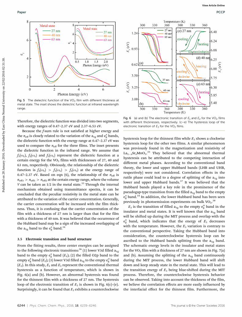
Therefore, the dielectric function was divided into two segments,with energy ranges of 0.47–2.37 eV and 2.37–6.53 eV.
Because the f-sum rule is not satisfied at higher energy andthe neff is closely related to the variation of the a1g and epg bands,the dielectric function with the energy range at 0.47–2.37 eV wasused to compare the neff for the three films. The inset presentsthe dielectric function in the infrared range. We assume thatf1(oc), f2(oc) and f3(oc) represent the dielectric function at acertain energy for the VO2 films with thicknesses of 27, 40 and63 nm, respectively. Obviously, the relationship of the dielectricfunction is f3(oc) 4 f1(oc) 4 f2(oc) at the energy range of0.47–2.37 eV. Based on eqn (6), the relationship of the neff isneff3 4 neff1 4 neff2 at the certain energy range, where the volumeV can be taken as 1/2 in the metal state.33 Through the internalmechanism obtained using transmittance spectra, it can beconcluded that the peculiar resistivity in the metal state can beattributed to the variation of the carrier concentration. Generally,the carrier concentration will be increased with the film thick-ness. Thus, it is confusing that the carrier concentration of thefilm with a thickness of 27 nm is larger than that for the filmwith a thickness of 40 nm. It was believed that the occurrence ofthe Hubbard band may be a sign of the increased overlapping ofthe a1g band to the epg band.34
3.5 Electronic transition and band structure
From the fitting results, three center energies can be assignedto the following electronic transitions:36 (1) lower V3d filled a1g
band to the empty epg band (E1); (2) the filled O2p band to theempty epg band (E2); (3) lower V3d filled a1g to the empty esg band(E3). In this study, E1 and E2 represent the conventional thermalhysteresis as a function of temperature, which is shown inFig. 6(a) and (b). However, an abnormal hysteresis was foundfor the thinnest film with a thickness of 27 nm. The hysteresisloop of the electronic transition of E3 is shown in Fig. 6(c)–(e).Surprisingly, it can be found that E3 exhibits a counterclockwise
hysteresis loop for the thinnest film while E3 shows a clockwisehysteresis loop for the other two films. A similar phenomenonwas previously found in the magnetization and resistivity ofLa1�xSrxMnO3.35 They believed that the abnormal thermalhysteresis can be attributed to the competing interaction ofdifferent metal phases. According to the conventional bandtheory, the lower and upper Hubbard bands (LHB and UHB,respectively) were not considered. Correlation effects in therutile phase could lead to a degree of splitting of the a1g intolower and upper Hubbard bands.37 It was believed that theHubbard bands played a key role in the prominence of thepseudogap-type transition from the filled a1g band to the emptyepg band.34 In addition, the lower Hubbard band has been seenpreviously in photoemission experiments on bulk VO2.38
E3 is the transition of filled a1g to the empty esg band in theinsulator and metal states. It is well known that the a1g bandwill be shifted up during the MIT process and overlap with theepg band, which indicates that the energy of E3 decreaseswith the temperature. However, the E3 variation is contrary tothe conventional perspective. Taking the Hubbard band intoconsideration, the counterclockwise hysteresis loop can beascribed to the Hubbard bands splitting from the a1g band.The schematic energy levels in the insulator and metal statesfor the VO2 film with a thickness of 27 nm are shown in Fig. 7(a)and (b). Assuming the splitting of the a1g band continuouslyduring the MIT process, the lower Hubbard band will shiftdown and keep steady state in the metal state. This will lead tothe transition energy of E3 being blue-shifted during the MITprocess. Therefore, the counterclockwise hysteresis behaviorcan be observed. Taking into account the thickness of the film,we believe the correlation effects are more easily influenced bythe interfacial effect for the thinnest film. Furthermore, the
Fig. 5 The dielectric function of the VO2 film with different thickness atmetal state. The inset shows the dielectric function at infrared wavelengthrange.
Fig. 6 (a) and (b) The electronic transition of E1 and E2 for the VO2 filmswith different thicknesses, respectively. (c–e) The hysteresis loop of theelectronic transition of E3 for the VO2 films.
Paper PCCP
Publ
ishe
d on
28
Janu
ary
2016
. Dow
nloa
ded
by E
ast C
hina
Nor
mal
Uni
vers
ity o
n 22
/02/
2016
02:
31:3
0.
View Article Online

This journal is© the Owner Societies 2016 Phys. Chem. Chem. Phys., 2016, 18, 6239--6246 | 6245
occurrence of the Hubbard bands may symbolize the increasedoverlapping of the a1g band to the epg band, which may be theorigin of the abnormal resistivity at the metal state. Therefore,the counterclockwise hysteresis loop of E3 can be observed forthe VO2 film with a thickness of 27 nm.
4 Conclusions
In summary, it was found that the spectral slopes in the near-infrared absorption region have a positive correlation with thephase transition magnitudes of the resistivity and transmittancefor VO2 films with different thicknesses. This finding is ofbenefit for discerning and forecasting the optical and electricalproperties of films from the macroscopic level. In addition,abnormal resistivity in the metal state was observed. The para-meters of the Drude model and the f-sum rule were applied toaccount for the phenomenon, which can be attributed to thevariation of the carrier concentration. Remarkably, the E3 energyexhibits a counterclockwise hysteresis loop with temperature forthe VO2 film with a thickness of 27 nm, which can be ascribed tothe occurrence of the Hubbard bands. It is believed that thelower Hubbard band may lead to the transition of E3 being blueshifted and symbolize the increased overlapping of the a1g bandwith the epg band.
Acknowledgements
This work was financially supported by the Major StateBasic Research Development Program of China (Grant No.2013CB922300 and 2011CB922200), the Natural Science Foun-dation of China (Grant No. 11374097, 61376129 and 61504156),the Projects of Science and Technology Commission of ShanghaiMunicipality (Grant No. 15JC1401600, 14XD1401500, 13JC1402100,and 13JC1404200), and the Program for Professor of SpecialAppointment (Eastern Scholar) at Shanghai Institutions of HigherLearning.
References
1 F. J. Morin, Phys. Rev. Lett., 1959, 3, 34–36.2 P. Baum, D. S. Yang and A. H. Zewail, Science, 2007, 318,
788–792.3 C. Kubler, H. Ehrke, R. Huber, R. Lopez, A. Halabica, R. F.
Haglund and A. Leitenstorfer, Phys. Rev. Lett., 2007, 99, 116401.4 D. Wegkamp, M. Herzog, L. Xian, M. Gatti, P. Cudazzo, C. L.
McGahan, R. E. Marvel, R. F. Haglund Jr, A. Rubio, M. Wolfand J. Sthler, Phys. Rev. Lett., 2014, 113, 216401.
5 R. M. Wentzcovitch, W. W. Schulz and P. B. Allen, Phys. Rev.Lett., 1994, 72, 3389.
6 T. M. Rice, H. Launojs and J. P. Pouget, Phys. Rev. Lett., 1994,73, 3042.
7 M. M. Qazilbash, M. Brehm, B. G. Chae, P. C. Ho, G. O. Andreev,B. J. Kim, S. J. Yun, A. V. Balatsky, M. B. Maple, F. Keilmann,H. T. Kim and D. N. Basov, Science, 2007, 318, 1750–1753.
8 L. Pellegrino, N. Manca, T. Kanki, H. Tanaka, M. Biasotti,E. Bellingeri, A. S. Siri and D. Marre, Adv. Mater., 2012, 24,2929–2934.
9 N. Shukla, A. V. Thathachary, A. Agrawal, H. Paik, A. Aziz,D. G. Schlom, S. K. Gupta, R. E. Herbert and S. Datta, Nat.Commun., 2015, 6, 7812.
10 Y. Zhou, J. Park, J. Shi, M. Chhowalla, H. Park, D. A. Weitzand S. Ramanathan, Nano Lett., 2015, 15, 1627–1634.
11 S. Chen, J. J. Liu, L. H. Wang, H. J. Luo and Y. F. Gao, J. Phys.Chem. C, 2014, 118, 18938–18944.
12 A. Tselev, J. D. Budai, E. Strelcov, J. Z. Tischler, A. Kolmakovand S. V. Kalinin, Nano Lett., 2011, 11, 3065–3073.
13 B. A. Nagaphani, X. G. Alexander, D. Marc, C. Matteo, G. Li,H. R. Alexander, K. Roopali, O. Hendrik, A. J. Catherine,A. Elke, P. R. Kevin, A. U. Hermann, G. S. Mahesh andS. P. P. Stuart, Nat. Phys., 2013, 9, 661–666.
14 T. X. Nan, M. Liu, W. Ren, Z. G. Ye and N. X. Sun, Sci. Rep.,2012, 4, 5931.
15 C. Marini, E. Arcangeletti, D. D. Castro, L. Baldassare,A. Perucchi, S. Lupi, L. Malavasi, L. Boeri, E. Pomjakushina,K. Conder and P. Postorino, Phys. Rev. B: Condens. Matter Mater.Phys., 2008, 77, 235111.
16 L. G. Bai, Q. Li, S. A. Corr, Y. Meng, C. Y. Park, S. V. Sinogeikin,C. Ko, J. Q. Wu and G. Y. Shen, Phys. Rev. B: Condens. MatterMater. Phys., 2015, 91, 104110.
17 P. Zhang, K. Jiang, Q. L. Deng, Q. H You, J. Z. Zhang,J. D. Wu, Z. G. Hu and J. H. Chu, J. Mater. Chem. C, 2015,3, 5033–5040.
18 D. Brassard, S. Fourmaux, M. J. Jacques, J. C. Kieffer andM. A. El Khakani, Appl. Phys. Lett., 2005, 87, 051910.
19 R. Molaei, R. Bayati, F. Wu and J. Narayan, J. Appl. Phys.,2014, 115, 164311.
20 K. Nagashima, T. Yanagida, H. Tanaka and T. Kawai, Phys.Rev. B: Condens. Matter Mater. Phys., 2006, 74, 172106.
21 X. Li, A. Gloter, H. Gu, X. Cao, P. Jin and C. Colliex, ActaMater., 2013, 61, 6443–6452.
22 S. Rathi, I. Lee, J. H. Park, B. J. Kim, H. T. Kim and G. H. Kim,ACS Appl. Mater. Interfaces, 2014, 6, 19718–19725.
23 Z. Yang and S. Ramanathan, Appl. Phys. Lett., 2011, 98, 192113.
Fig. 7 (a) and (b) Schematic energy levels in the insulator and metal statesfor the VO2 film with a thickness of 27 nm, respectively.
PCCP Paper
Publ
ishe
d on
28
Janu
ary
2016
. Dow
nloa
ded
by E
ast C
hina
Nor
mal
Uni
vers
ity o
n 22
/02/
2016
02:
31:3
0.
View Article Online

6246 | Phys. Chem. Chem. Phys., 2016, 18, 6239--6246 This journal is© the Owner Societies 2016
24 Q. W. Shi, W. X. Huang, Y. X. Zhang, J. Z. Yan, Y. B. Zhang,M. Mao, Y. Zhang and M. J. Tu, ACS Appl. Mater. Interfaces,2011, 3, 3523–3527.
25 N. F. Quackenbush, J. W. Tashman, J. A. Mundy, S. Sallis,H. Paik, R. Misra, J. A. Moyer, J. H. Guo, D. A. Fischer,J. C. Woicik, D. A. Muller, D. G. Schlom and L. F. J. Piper,Nano Lett., 2013, 13, 4857–4861.
26 C. H. Chen and Z. Y. Fan, Appl. Phys. Lett., 2009, 95, 262106.27 M. Li, X. Wu, L. Li, Y. X. Wang, D. B. Li, J. Pan, S. J. Li,
L. T. Sun and G. H. Li, J. Mater. Chem. A, 2014, 2, 4520–4523.28 W. T. Liu, J. Cao, W. Fan, Z. Hao, M. C. Martin, Y. R. Shen,
J. Wu and F. Wang, Nano Lett., 2011, 11, 466–470.29 W. W. Li, Q. Yu, J. R. Liang, K. Jiang, Z. G. Hu, J. Liu,
H. D. Chen and J. H. Chu, Appl. Phys. Lett., 2011, 99, 241903.30 A. Gavinit and C. C. Y. Kwan, Phys. Rev. B: Solid State, 1972,
5, 3138.31 H. W. Verleur, A. S. Barker and C. N. Berglund, Phys. Rev.,
1968, 172, 788–798.
32 K. Okazaki, H. Wadati, A. Fujimori, M. Onoda, Y. Muraokaand Z. Hiroi, Phys. Rev. B: Condens. Matter Mater. Phys.,2004, 69, 165104.
33 D. B. Mcwhan, M. Marezio, J. P. Remeika and P. D. Dernier,Phys. Rev. B: Solid State, 1974, 10, 490.
34 T. J. Huffman, P. Xu, A. J. Hollingshad, M. M. Qazilbash,L. Wang, R. A. Lukaszew, S. Kittiwatanakul, J. Lu and S. A.Wolf, Phys. Rev. B: Condens. Matter Mater. Phys., 2015, 91, 205140.
35 J. Dho, W. S. Kim and N. H. Hur, Phys. Rev. Lett., 2001,87, 187201.
36 W. W. Li, J. J. Zhu, X. F. Xu, K. Jiang, Z. G. Hu, M. Zhu andJ. H. Chu, J. Appl. Phys., 2011, 110, 013504.
37 S. Biermann, A. Georges, A. Lichtenstein and T. Giamarchi,Phys. Rev. Lett., 2001, 87, 276405.
38 T. C. Koethe, Z. Hu, M. W. Haverkort, C. S. Langeheine,F. Venturini, N. B. Brookes, O. Tjernberg, W. Reichelt,H. H. Hsieh, H. J. Lin, C. T. Chen and L. H. Tjeng, Phys.Rev. Lett., 2006, 97, 116402.
Paper PCCP
Publ
ishe
d on
28
Janu
ary
2016
. Dow
nloa
ded
by E
ast C
hina
Nor
mal
Uni
vers
ity o
n 22
/02/
2016
02:
31:3
0.
View Article Online