solid baffle and background update zhiwen zhao uva 2013/05/23
TRANSCRIPT

SoLID Baffle and Background Update
Zhiwen ZhaoUVa
2013/05/23

PVDIS challenge
• High luminosity (1.27e39/cm2/s for 50uA on 40cm LD2 target) causes high rate and high energy dose on detectors
• Baffle shields low energy EM photons directly from target while low energy electrons are bent away by field
• Most interesting physics at high Q2 and high x needs DIS electrons with highest energy which bend least and fly like photons, so comprise is needed
• Positive pions contribute in background at trigger level and are better to be suppressed

3
Design Condition• SoLID latest CLEOv8 field map• 30 sectors with each sector covering 12 deg• each plate is 9cm thick lead• Z (40, 68, 96, 124, 152, 180) cm • no overlap with current setup
• Rin (4.00, 12.86, 23.61, 34.36, 45.10, 55.85)cm• Rout (39.60, 59.94, 80.28, 100.63, 120.97, 141.31)cm• Optimized for polar angle 21-36 deg acceptance of
full 40cm long target with center at 10cm, except the first baffle inner radius needs to be at 4cm instead of 2cm to avoid more EM background

4
Current Baffle(Smaller Z baffle cut inner)
• Continue with Seamus’s approach, but take all design conditions into account– refer to
• https://hallaweb.jlab.org/wiki/index.php/Baffle_Design• https://hallaweb.jlab.org/wiki/index.php/Solid_design_FOM

General acceptancenegative neutral positive
30%20%
5%
20%
eDIS acceptance
40%
50%

Apv Error• 50uA 85% polarized 11GeV beam on 40cm
LD2 for 120 days• Trigger at 2GeV
BaBar field and baffle, from proposal CLEO field and baffle, from proposal

7
Trigger effectApvErr trigger
(GeV)0.17,0.24,0.36,0.38,0.42,0.39,0.48,0.44,0.56,0.51,0.66,0.64,0.75,0.70,0.67 0.00.20,0.26,0.36,0.40,0.42,0.40,0.48,0.44,0.56,0.51,0.66,0.64,0.75,0.70,0.67 1.50.27,0.31,0.37,0.62,0.45,0.51,0.48,0.51,0.56,0.54,0.66,0.65,0.75,0.70,0.67 2.00.38,0.37,0.39,0.96,0.42,0.74,0.48,0.65,0.56,0.65,0.66,0.75,0.75,0.74,0.67 2.30.53,0.43,0.43,1.46,0.44,1.03,0.48,0.86,0.56,0.80,0.66,0.89,0.75,0.83,0.69 2.52.13,0.84,0.63,0.00,0.56,9.22,0.56,2.83,0.60,2.14,0.68,1.97,0.75,1.40,0.81 3.0
trigger 2.0 trigger 2.3
ApvErr at large Q2 and large x starts to increase if trigger > 2GeV

Trigger effect ApvErr trigger (GeV)0.28,0.32,0.38,0.63,0.42,0.52,0.49,0.52,0.57,0.55,0.67,0.66,0.75,0.72,0.68 p<2.0, r(110cm – 270cm)
1.90,0.58,0.44,0.72,0.43,0.53,0.49,0.52,0.57,0.55,0.67,0.66,0.75,0.72,0.68 p<3.0, r(110cm – 140cm) p<2.5 ,r(140cm – 170cm)p<2.0, r (170cm – 270cm)
0.52,0.42,0.41,0.72,0.43,0.53,0.49,0.52,0.57,0.55,0.67,0.66,0.75,0.72,0.68 p<2.5, r(110cm – 170cm) p<2.0, r(170cm – 270cm)
p<2.0, r(110cm – 270cm) p<2.5, r(110cm – 170cm) p<2.0, r(170cm – 270cm)
This could an option for trigger

Background, baffle effect
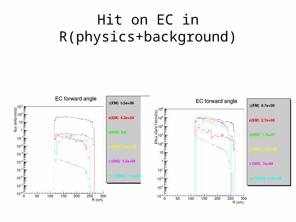
Hit on EC in R(physics+background)

Hit on EC in Phi(physics+background)

GEM geometry

13
PVDIS GEMid Z
(cm)
PVDIS target center PVDIS target full
R range(cm)
Area(m2)
R range(cm)
Area(m2)
1 157.5 56-107 2.6116 48-122 3.9521
2 185.5 67-128 3.7369 59-143 5.3307
3 306 113-215 10.5105 105-230 13.1554
4 315 117-222 11.1824 109-237 13.9135
total 28.0414 36.3517
• CLEO coil center at 0.• PVDIS 40cm long target with center at 10cm• PVDIS angle 21-36 degree• Considering the CLEO baffle, plane 1 and 2 are directly behind baffle and only
need partial coverage (70-80%?), plane 3 and 4 are between Cherenkov and EC and need full coverage
• To cover full target, GEM needs to increase by 30%

14
SIDIS/JPsi GEM
id Z(cm)
SIDIS target center SIDIS target full JPsi target center
R range(cm)
Area(m2)
R range(cm)
Area(m2)
R rangeneeded
(cm)
Area needed
(m2)
Area addition
to “SIDIS target
center”(m2)
Area addition
to “SIDIS target full”
(m2)
1 -175 46-78 1.2466 41-87 1.8498 36-67 1.0031 0.2576 0.1210
2 -150 26-91 2.3892 23-98 2.8510 21-80 1.8720 0.0738 0.0276
3 -119 30-103 3.0502 27-112 3.7118 25-97 2.7595 0.0864 0.0327
4 -68 37-126 4.5575 34-135 5.3624 32-123 4.4312 0.1084 0.0415
5 5 46-95 2.1705 44-100 2.5334 42-90 1.9905 0.1106 0.0540
6 92 58-118 3.3175 55-123 3.8026 55-115 3.2044 0.1065 0.0000
total 16.7315 20.1110 15.2607 0.7433(4.5%)
0.2768(1.4%)
• CLEO coil center at 0.• Plane (1,2,3,4) cover large angle and plane (2,3,4,5,6) cover forward angle• SIDIS 40cm long target with center at -350cm, SIDIS angle 7.5-14.85-24 degree• JPsi 15cm long target with center at -300cm tentatively, JPsi angle 8- 16.28-28 degree• Jpsi coverage is only optimized by target center as it’s length is smaller• GEM size determined by “Jpsi target center” inner and “SIDIS target full” outer• PVDIS has more than enough GEM for SIDIS/JPsi to cover full target

backup

16
Design Detail• Common
– use SoLID CLEOv8 field map– 30 sectors with each sector covering 12 deg– Still each plate is 9cm thick of lead– SCALE MIN=1.4, MAX=1.4, LASTBAF=0. in makebaf5.C
• Larger Z baffle only– Z (40, 70, 100, 130, 160, 190) cm
• overlap with Cherenkov and leaves no room for GEM
– Rin (3.90, 15.30, 26.60, 37.90, 49.20, 61.01)cm– Rout (41.31, 62.32, 83.32, 104.33, 125.34, 142.00)cm
• Not optimized for polar angle 21-36 deg acceptance of full 40cm long target with center at 10cm
• Smaller Z baffle only– Z (40, 68, 96, 124, 152, 180) cm
• no overlap with current setup
– Rin (2.11, 12.86, 23.61, 34.36, 45.10, 55.85)cm– Rout (39.60, 59.94, 80.28, 100.63, 120.97, 141.31)cm
• Optimized for polar angle 21-36 deg acceptance of full 40cm long target with center at 10cm

17
Design approachfrom larger Z baffle to smaller Z baffle
• Continue with Seamus’s approach– In simulation, throw negative particles from target position with field, record tracks at different
position– Then do linear fitting to figure out what kind of blocking should be at the assumed baffle plates
position.– Output the opening (not block)– refer to
• https://hallaweb.jlab.org/wiki/index.php/Baffle_Design• https://hallaweb.jlab.org/wiki/index.php/Solid_design_FOM
• Fix a bug of detector plane position in the input file• Change Z, Rin, Rout to the desired values

eDIS rate