solar-led streetlight controller with 25 w led lamp … · solar-led streetlight controller with 25...
TRANSCRIPT

September 2010 Doc ID 15473 Rev 2 1/38
AN2946Application note
Solar-LED streetlight controller with 25 W LED lamp driverand 85 W battery charger based on the STM32F101Rx
IntroductionThe solar-LED streetlight controller described in this application note is designed to achieve an 85 W solar energy battery charger and a 25 W LED lamp driver. During the daytime the controller preserves the electricity energy gathered by the solar module (PV module), then stores it in the battery. In the evening the controller uses the battery energy to power the LED streetlight. When the battery runs out of power after several rainy days, the controller enables the external offline power supply (not included in this system) instead of the battery to power the LED streetlight until the system battery is fully charged again.
Due to the clean nature of solar energy, and the highly efficient energy conversion of the PV module and very long operating life of the LED lamp, the solar-LED streetlight controller, compared to conventional streetlights, can save electricity remarkably, thus abating greenhouse gas (e.g. CO2) emission.
This application note is based on the solution of solar-LED streetlight controller architecture, including a battery charger and LED lamp driver. The description of the architecture involves hardware and firmware design with design parameter settings. The solar-LED streetlight controller demonstration board is shown in Figure 1.
Figure 1. Solar-LED streetlight controller demonstration board
www.st.com

Contents AN2946
2/38 Doc ID 15473 Rev 2
Contents
1 Safety instructions . . . . . . . . . . . . . . . . . . . . . . . . . . . . . . . . . . . . . . . . . . 5
1.1 Intended use . . . . . . . . . . . . . . . . . . . . . . . . . . . . . . . . . . . . . . . . . . . . . . . 5
1.2 Installation . . . . . . . . . . . . . . . . . . . . . . . . . . . . . . . . . . . . . . . . . . . . . . . . . 5
1.3 Electrical connection . . . . . . . . . . . . . . . . . . . . . . . . . . . . . . . . . . . . . . . . . 5
1.4 Board operation . . . . . . . . . . . . . . . . . . . . . . . . . . . . . . . . . . . . . . . . . . . . . 5
2 General description . . . . . . . . . . . . . . . . . . . . . . . . . . . . . . . . . . . . . . . . . . 6
2.1 Controller features . . . . . . . . . . . . . . . . . . . . . . . . . . . . . . . . . . . . . . . . . . . 6
2.2 Solar-LED streetlight system architecture . . . . . . . . . . . . . . . . . . . . . . . . . 6
2.3 Scope of the solar-LED streetlight controller . . . . . . . . . . . . . . . . . . . . . . . 7
2.4 Main functions of the controller . . . . . . . . . . . . . . . . . . . . . . . . . . . . . . . . . 8
2.4.1 Battery charging management . . . . . . . . . . . . . . . . . . . . . . . . . . . . . . . . . 8
2.4.2 LED lamp driving management . . . . . . . . . . . . . . . . . . . . . . . . . . . . . . . . 9
2.4.3 System monitoring circuit . . . . . . . . . . . . . . . . . . . . . . . . . . . . . . . . . . . . . 9
3 Hardware design . . . . . . . . . . . . . . . . . . . . . . . . . . . . . . . . . . . . . . . . . . . 10
3.1 Circuit description . . . . . . . . . . . . . . . . . . . . . . . . . . . . . . . . . . . . . . . . . . . 10
3.1.1 Power supply circuit . . . . . . . . . . . . . . . . . . . . . . . . . . . . . . . . . . . . . . . . 10
3.1.2 Electricity power collection . . . . . . . . . . . . . . . . . . . . . . . . . . . . . . . . . . . 11
3.1.3 LED lamp driving circuit . . . . . . . . . . . . . . . . . . . . . . . . . . . . . . . . . . . . . 13
3.1.4 Analog signal acquisition circuit . . . . . . . . . . . . . . . . . . . . . . . . . . . . . . . 14
3.2 Test results . . . . . . . . . . . . . . . . . . . . . . . . . . . . . . . . . . . . . . . . . . . . . . . . 15
3.2.1 Battery charger . . . . . . . . . . . . . . . . . . . . . . . . . . . . . . . . . . . . . . . . . . . 15
3.2.2 LED driver . . . . . . . . . . . . . . . . . . . . . . . . . . . . . . . . . . . . . . . . . . . . . . . 19
4 Firmware design . . . . . . . . . . . . . . . . . . . . . . . . . . . . . . . . . . . . . . . . . . . 21
4.1 Main loop . . . . . . . . . . . . . . . . . . . . . . . . . . . . . . . . . . . . . . . . . . . . . . . . . 22
4.2 Battery charging management . . . . . . . . . . . . . . . . . . . . . . . . . . . . . . . . . 23
4.2.1 MPPT principle . . . . . . . . . . . . . . . . . . . . . . . . . . . . . . . . . . . . . . . . . . . 23
4.2.2 Battery charging management . . . . . . . . . . . . . . . . . . . . . . . . . . . . . . . . 25
4.3 LED lamp driving management . . . . . . . . . . . . . . . . . . . . . . . . . . . . . . . . 26
4.4 System monitoring management . . . . . . . . . . . . . . . . . . . . . . . . . . . . . . . 27

AN2946 Contents
Doc ID 15473 Rev 2 3/38
5 Overview of demonstration board . . . . . . . . . . . . . . . . . . . . . . . . . . . . . 30
5.1 Application schematic . . . . . . . . . . . . . . . . . . . . . . . . . . . . . . . . . . . . . . . . 30
5.2 Application board . . . . . . . . . . . . . . . . . . . . . . . . . . . . . . . . . . . . . . . . . . . 31
5.3 Bill of material . . . . . . . . . . . . . . . . . . . . . . . . . . . . . . . . . . . . . . . . . . . . . . 32
6 References . . . . . . . . . . . . . . . . . . . . . . . . . . . . . . . . . . . . . . . . . . . . . . . . 36
7 Revision history . . . . . . . . . . . . . . . . . . . . . . . . . . . . . . . . . . . . . . . . . . . 37

List of figures AN2946
4/38 Doc ID 15473 Rev 2
List of figures
Figure 1. Solar-LED streetlight controller demonstration board . . . . . . . . . . . . . . . . . . . . . . . . . . . . . . 1Figure 2. Solar-LED streetlight system . . . . . . . . . . . . . . . . . . . . . . . . . . . . . . . . . . . . . . . . . . . . . . . . 6Figure 3. System block diagram . . . . . . . . . . . . . . . . . . . . . . . . . . . . . . . . . . . . . . . . . . . . . . . . . . . . . 7Figure 4. Battery charging pattern . . . . . . . . . . . . . . . . . . . . . . . . . . . . . . . . . . . . . . . . . . . . . . . . . . . . 8Figure 5. LED lamp driving scheme. . . . . . . . . . . . . . . . . . . . . . . . . . . . . . . . . . . . . . . . . . . . . . . . . . . 9Figure 6. 12 V power supply circuit . . . . . . . . . . . . . . . . . . . . . . . . . . . . . . . . . . . . . . . . . . . . . . . . . . 10Figure 7. 3.3 V power supply circuit . . . . . . . . . . . . . . . . . . . . . . . . . . . . . . . . . . . . . . . . . . . . . . . . . . 10Figure 8. Noise filtering circuit for VDD and VDDA . . . . . . . . . . . . . . . . . . . . . . . . . . . . . . . . . . . . . . 11Figure 9. Solar module control circuit . . . . . . . . . . . . . . . . . . . . . . . . . . . . . . . . . . . . . . . . . . . . . . . . 11Figure 10. Hardware OVP circuit for battery overcharging protection . . . . . . . . . . . . . . . . . . . . . . . . . 12Figure 11. Battery charger circuit . . . . . . . . . . . . . . . . . . . . . . . . . . . . . . . . . . . . . . . . . . . . . . . . . . . . . 12Figure 12. LED lamp driver circuit . . . . . . . . . . . . . . . . . . . . . . . . . . . . . . . . . . . . . . . . . . . . . . . . . . . . 14Figure 13. Temperature sensing circuits . . . . . . . . . . . . . . . . . . . . . . . . . . . . . . . . . . . . . . . . . . . . . . . 15Figure 14. Voltage and current detection circuit . . . . . . . . . . . . . . . . . . . . . . . . . . . . . . . . . . . . . . . . . 15Figure 15. Charging current versus solar module output voltage . . . . . . . . . . . . . . . . . . . . . . . . . . . . 16Figure 16. MPPT test diagram . . . . . . . . . . . . . . . . . . . . . . . . . . . . . . . . . . . . . . . . . . . . . . . . . . . . . . . 16Figure 17. V-I curve and PSC . . . . . . . . . . . . . . . . . . . . . . . . . . . . . . . . . . . . . . . . . . . . . . . . . . . . . . . 17Figure 18. Battery voltage versus charging current . . . . . . . . . . . . . . . . . . . . . . . . . . . . . . . . . . . . . . . 18Figure 19. Charger input current (Isc) . . . . . . . . . . . . . . . . . . . . . . . . . . . . . . . . . . . . . . . . . . . . . . . . . 19Figure 20. Charger output current (Iba) . . . . . . . . . . . . . . . . . . . . . . . . . . . . . . . . . . . . . . . . . . . . . . . . 19Figure 21. Vds on Q2, current on L2, and Vak on D4 . . . . . . . . . . . . . . . . . . . . . . . . . . . . . . . . . . . . . 19Figure 22. LED lamp current, efficiency vs. battery voltage. . . . . . . . . . . . . . . . . . . . . . . . . . . . . . . . . 19Figure 23. LED current, efficiency vs. LED voltage . . . . . . . . . . . . . . . . . . . . . . . . . . . . . . . . . . . . . . . 20Figure 24. Driver input current . . . . . . . . . . . . . . . . . . . . . . . . . . . . . . . . . . . . . . . . . . . . . . . . . . . . . . . 20Figure 25. Driver output current . . . . . . . . . . . . . . . . . . . . . . . . . . . . . . . . . . . . . . . . . . . . . . . . . . . . . . 20Figure 26. Vgs, Ids, and Vds on Q4. . . . . . . . . . . . . . . . . . . . . . . . . . . . . . . . . . . . . . . . . . . . . . . . . . . 20Figure 27. Main loop flowchart . . . . . . . . . . . . . . . . . . . . . . . . . . . . . . . . . . . . . . . . . . . . . . . . . . . . . . . 22Figure 28. 80 W solar module I-V and P-V curve . . . . . . . . . . . . . . . . . . . . . . . . . . . . . . . . . . . . . . . . 23Figure 29. P and O method . . . . . . . . . . . . . . . . . . . . . . . . . . . . . . . . . . . . . . . . . . . . . . . . . . . . . . . . . 23Figure 30. P and O tracing route . . . . . . . . . . . . . . . . . . . . . . . . . . . . . . . . . . . . . . . . . . . . . . . . . . . . . 24Figure 31. Three-stage charging routine . . . . . . . . . . . . . . . . . . . . . . . . . . . . . . . . . . . . . . . . . . . . . . . 25Figure 32. MPPT flowchart . . . . . . . . . . . . . . . . . . . . . . . . . . . . . . . . . . . . . . . . . . . . . . . . . . . . . . . . . 25Figure 33. Ambient light sensing flowchart (day and night judgment) . . . . . . . . . . . . . . . . . . . . . . . . . 26Figure 34. LED light-off routine . . . . . . . . . . . . . . . . . . . . . . . . . . . . . . . . . . . . . . . . . . . . . . . . . . . . . . 26Figure 35. LED light-on routine . . . . . . . . . . . . . . . . . . . . . . . . . . . . . . . . . . . . . . . . . . . . . . . . . . . . . . 27Figure 36. System monitoring flowchart. . . . . . . . . . . . . . . . . . . . . . . . . . . . . . . . . . . . . . . . . . . . . . . . 27Figure 37. LED_fault IRQ flowchart . . . . . . . . . . . . . . . . . . . . . . . . . . . . . . . . . . . . . . . . . . . . . . . . . . . 28Figure 38. System self-recovery flowchart . . . . . . . . . . . . . . . . . . . . . . . . . . . . . . . . . . . . . . . . . . . . . . 28Figure 39. Anti-backflow for battery charging flowchart . . . . . . . . . . . . . . . . . . . . . . . . . . . . . . . . . . . . 29Figure 40. Schematic . . . . . . . . . . . . . . . . . . . . . . . . . . . . . . . . . . . . . . . . . . . . . . . . . . . . . . . . . . . . . . 30Figure 41. Top view of demonstration board . . . . . . . . . . . . . . . . . . . . . . . . . . . . . . . . . . . . . . . . . . . . 31Figure 42. Bottom view of demonstration board . . . . . . . . . . . . . . . . . . . . . . . . . . . . . . . . . . . . . . . . . 31

AN2946 Safety instructions
Doc ID 15473 Rev 2 5/38
1 Safety instructions
Warning: The demonstration board must be used in a suitable laboratory by qualified personnel only who are familiar with the installation, use, and maintenance of electrical systems.
1.1 Intended useThe demonstration board is a component designed for demonstration purposes only, and shall be used neither for domestic installation nor for industrial installation. The technical data as well as the information concerning the power supply and operating conditions shall be taken from the documentation included with the demonstration board and strictly observed.
1.2 InstallationThe installation of the demonstration board shall be taken from the present document and strictly observed. The components must be protected against excessive strain. In particular, no components are to be bent, or isolating distances altered during the transportation, handling or usage. The demonstration board contains electrostatically-sensitive components that are prone to damage through improper use. Electrical components must not be mechanically damaged or destroyed (to avoid potential risks and health injury).
1.3 Electrical connectionApplicable national accident prevention rules must be followed when working on the mains power supply. The electrical installation shall be completed in accordance with the appropriate requirements (e.g. cross-sectional areas of conductors, soldering, and PE connections).
1.4 Board operationA system architecture which supplies power to the demonstration board shall be equipped with additional control and protective devices in accordance with the applicable safety requirements (e.g. compliance with technical equipment and accident prevention rules).

General description AN2946
6/38 Doc ID 15473 Rev 2
2 General description
2.1 Controller features● MPPT maximizes solar module efficacy
● Automatic day and night detection
● Automatic mains switch enable function when battery low
● Constant current control for LED lamp
● Battery charge control
● Optional LED lighting mode
● LED indicators for system status monitoring and debugging status
● Full protection function for OVP, UVP, OCP, and OTP.
2.2 Solar-LED streetlight system architectureThe solar-LED streetlight controller not only controls solar energy storage to the battery, but it also manages the power consumption to the LED streetlight. The system architecture of the solar-LED streetlight system is illustrated in Figure 2.
Figure 2. Solar-LED streetlight system
AN2946 General description
Doc ID 15473 Rev 2 7/38
1. The sunlight delivers rays of photons (solar energy) which hit the solar panel (Photovoltaic or PV module). The photons (energy) are absorbed by the PV and electrons are released.
2. The electrons flow along the metal contact of the PV and form electricity.
3. Energy is stored in the battery during daytime and consumed at night.
4. The LED lamp (LED streetlight) is driven to operate by the LED lamp driver. This controller monitors the system and manages the light-on and light-off in day and night time.
5. When the battery goes low, the controller sends an enable signal to the 'Mains switch' which enables the AC offline power supply.
6. The AC offline power supply (not included in this application note) works as a backup source to power the LED streetlight.
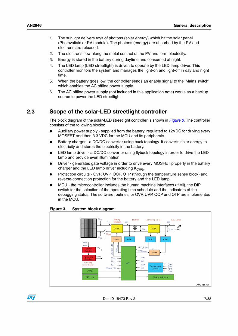
2.3 Scope of the solar-LED streetlight controllerThe block diagram of the solar-LED streetlight controller is shown in Figure 3. The controller consists of the following blocks:
● Auxiliary power supply - supplied from the battery, regulated to 12VDC for driving every MOSFET and then 3.3 VDC for the MCU and its peripherals.
● Battery charger - a DC/DC converter using buck topology. It converts solar energy to electricity and stores the electricity in the battery.
● LED lamp driver - a DC/DC converter using flyback topology in order to drive the LED lamp and provide even illumination.
● Driver - generates gate voltage in order to drive every MOSFET properly in the battery charger and the LED lamp driver including KCHG.
● Protection circuits - OVP, UVP, OCP, OTP (through the temperature sense block) and reverse-connection protection for the battery and the LED lamp.
● MCU - the microcontroller includes the human machine interfaces (HMI), the DIP switch for the selection of the operating time schedule and the indicators of the debugging status. The software routines for OVP, UVP, OCP and OTP are implemented in the MCU.
Figure 3. System block diagram

General description AN2946
8/38 Doc ID 15473 Rev 2
The MCU implements the sophisticated peripherals as listed in Table 1.
2.4 Main functions of the controller
2.4.1 Battery charging management
During the daytime, the battery is charged by PV electricity according to the typical pattern. An MPPT (maximum power point tracing) algorithm is applied to enable the PV module to output as much electricity power as it can. Refer to Section 4.2 for more information concerning MPPT. The pattern for the 12 V battery system is shown in Figure 4. The pattern differentiates the entire charging process into 3 stages. During stage 1 and stage 2, the battery is charged with the solar module maximum power. In stage 3, the battery is charged in constant voltage algorithm.
Figure 4. Battery charging pattern
● Stage 1 (trickle charging): UBAT < 11 V. The battery is charged with the maximum power of the PV module. This stage is designed for a battery which is deeply
Table 1. MCU peripheral allocation
Peripheral Number Description
ADC 11 USC+, USC-, UBAT, ULED, ISC, IBAT, ILED, TCHG, TBAT, TDRV, TLED
GPIO 12 Inputs DIP1~4 (up to 16 modes) JTAG
Status indication
Charger_EN for anti-backflow chargeMains_EN for switching to mains supply
Battery LED1-2 for indicating battery status
Debug LED1-4 for diagnosis (up to 16 messages)
PWM 2 PWMCHG, PWMDRV (100 kHz)
EXT1 1 LED fault
AN2946 General description
Doc ID 15473 Rev 2 9/38
discharged. In order to prolong battery operating life, the charging current is constrained at Imax = 0.5 A.
● Stage 2 (high-current bulk charging): 11 V ≤ UBAT < 14.3 V. In this stage, the battery is charged with the maximum power of the PV module. The charging current (Imp) may not be constant.
● Stage 3 (floating charging): UBAT ≥ 14.3 V. In this stage, battery is charged at constant voltage (14.3 V).
The voltage values 11 V and 14.3 V define the boundaries of the stages that are based on the characteristics of a typical 12 V lead acid battery. The voltage needed depends on the type of battery.
2.4.2 LED lamp driving management
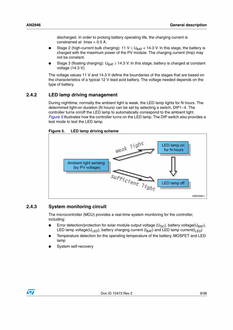
During nighttime, normally the ambient light is weak, the LED lamp lights for N hours. The determined light-on duration (N hours) can be set by selecting a switch, DIP1~4. The controller turns on/off the LED lamp to automatically correspond to the ambient light. Figure 5 illustrates how the controller turns on the LED lamp. The DIP switch also provides a test mode to test the LED lamp.
Figure 5. LED lamp driving scheme
2.4.3 System monitoring circuit
The microcontroller (MCU) provides a real-time system monitoring for the controller, including:
● Error detection/protection for solar module output voltage (USC), battery voltage(UBAT), LED lamp voltage(ULED), battery charging current (IBAT) and LED lamp current(ILED)
● Temperature detection for the operating temperature of the battery, MOSFET and LED lamp
● System self-recovery

Hardware design AN2946
10/38 Doc ID 15473 Rev 2
3 Hardware design
3.1 Circuit description
3.1.1 Power supply circuit
The system auxiliary power supply can be built with a 12 V battery. In order to drive the power MOSFET and some analog ICs perfectly, a regulated 12 V is required. The 12 V power supply schematic is shown in Figure 6.
Figure 6. 12 V power supply circuit
The MCU requires a 3.3 V source which is obtained from the output of the linear regulator (U11), see Figure 7 .
Figure 7. 3.3 V power supply circuit
Since the 3.3 V supply is mainly for the MCU, a proper filter, which avoids high-frequency switching noise interference between the digital power supply (VDD) and analog power supply (VDDA), is strongly recommended. The filter circuit is shown in Figure 8.
AN2946 Hardware design
Doc ID 15473 Rev 2 11/38
Figure 8. Noise filtering circuit for VDD and VDDA
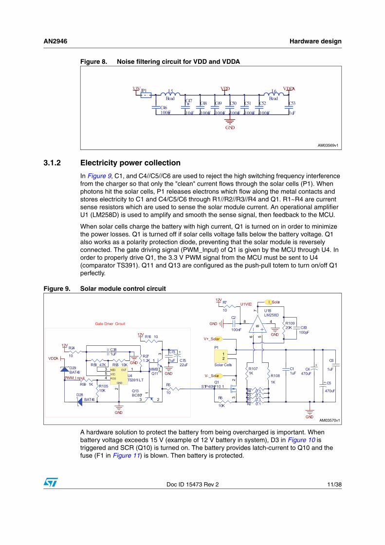
3.1.2 Electricity power collection
In Figure 9, C1, and C4//C5//C6 are used to reject the high switching frequency interference from the charger so that only the "clean" current flows through the solar cells (P1). When photons hit the solar cells, P1 releases electrons which flow along the metal contacts and stores electricity to C1 and C4/C5/C6 through R1//R2//R3//R4 and Q1. R1~R4 are current sense resistors which are used to sense the solar module current. An operational amplifier U1 (LM258D) is used to amplify and smooth the sense signal, then feedback to the MCU.
When solar cells charge the battery with high current, Q1 is turned on in order to minimize the power losses. Q1 is turned off if solar cells voltage falls below the battery voltage. Q1 also works as a polarity protection diode, preventing that the solar module is reversely connected. The gate driving signal (PWM_Input) of Q1 is given by the MCU through U4. In order to properly drive Q1, the 3.3 V PWM signal from the MCU must be sent to U4 (comparator TS391). Q11 and Q13 are configured as the push-pull totem to turn on/off Q1 perfectly.
Figure 9. Solar module control circuit
A hardware solution to protect the battery from being overcharged is important. When battery voltage exceeds 15 V (example of 12 V battery in system), D3 in Figure 10 is triggered and SCR (Q10) is turned on. The battery provides latch-current to Q10 and the fuse (F1 in Figure 11) is blown. Then battery is protected.

Hardware design AN2946
12/38 Doc ID 15473 Rev 2
Figure 10. Hardware OVP circuit for battery overcharging protection
The schematic of the battery charger is shown in Figure 11 which is based on buck topology. Q2, D4 are the buck MOSFET and diode, respectively. L2 is the inductor and C13 is the output capacitor. The charger operates in a continuous current mode so that small output current ripple is achieved and a small output capacitor can be used. C10 and C11 are used as a snubber to suppress high voltage spikes.
Since Q2 is floating and high-side transformer T2 is used to drive the MOSFET, the gate driving circuit is similar to the one shown in Figure 9.
Resistors R9, R17 ~ R20 and R55 are used to sense the charge current to the battery. U3 (TSC101) is the high-side current sensor which amplifies the signal and gives feedback to the MCU.
P2 is the connector to the battery. One fuse (F1) is in series with the battery to prevent catastrophic failure. To prevent reverse connection of the battery, one Schottky diode D14 is added. F1 blows out with D14 if the battery is reversely connected. This helps to protect the rest of the circuits.
Figure 11. Battery charger circuit

AN2946 Hardware design
Doc ID 15473 Rev 2 13/38
3.1.3 LED lamp driving circuit
The LED lamp driver is designed with flyback topology. No isolation is required in this application. Flyback is suitable for a wide ratio range of output voltage to input voltage. The battery voltage is 11 V ~ 14.3 V while for the LED lamp, which is connected in a 3*7 matrix (3 LED lamps in series and 7 strings in parallel), the maximum LED voltage is defined as 12 V. The flyback converter keeps the LED current constant in the above-mentioned battery voltage range. In Figure 12, T1 is the flyback transformer and Q4 is the power MOSFET. D5 and D9 clamp the maximum voltage across Q4 in the off-state. D10 acts as the output rectifier and C30 and C33 are the output capacitors. R46, R47 and U9 are used to sense the LED lamp current and feedback to the MCU for constant current regulation. The PWM signal from the MCU is converted from TTL level to CMOS level via U2 and amplified by Q7 and Q8 to drive Q4. When OCP and/or OVP activate, Q3 and Q9 are used to guarantee a single turn-on within each switching cycle. The MOSFET current is sensed by resistors R30, R33 and R54 and amplified by U5B. The output of U5B is used to achieve OCP. There are two levels of OCP implemented in the LED lamp driver. The MOSFET current is sensed and transferred to comparators U7A and U7B. U7B sets the first current limit which is activated cycle by cycle. R37 and R36 form a voltage divider and set the threshold at the negative input of U7B. Overcurrent in the primary circuit of T1 results in high logic output of U7B, thus pulling down the voltage of the 'LED_Protection' node at the Q5 collector. Consequently, comparator U2 outputs low voltage and forces Q4 to shut down. In case a heavy overload or short-circuit occurs, such as a physical short-circuit of T1 or D10 which might exist for some time, a second level OCP is needed to protect the driver. R41 and R43 form another voltage divider and set a higher threshold. A high current spike from Q4 triggers the threshold and U7A generates 'LED_Fault' interrupt to the MCU. After receiving continuous interrupts, the MCU stops outputting the 'PWM_Driver' signal and waits for a certain time for the next try (refer to Section 4.4). Such burst mode operation definitely lowers the voltage stress and current stress on power components. The OVP of the LED lamp is achieved by D12. The principal is similar to that of the first level of OCP.

Hardware design AN2946
14/38 Doc ID 15473 Rev 2
Figure 12. LED lamp driver circuit
3.1.4 Analog signal acquisition circuit
The operating voltage, current and temperature of the battery and LED lamp are monitored by the MCU. The temperature sensing circuits are illustrated in Figure 13. The voltage and current sensing circuits are shown in Figure 14. For the battery charger and LED lamp driver, NTC(s) is soldered on the heat sink of MOSFET (or rectifier). The operating temperature of the MOSFET (or rectifier) is sensed via NTC(s) and sent to the MCU. These key power components are protected against overtemperature. For the battery and LED lamp, the sensing NTC(s) is applied on the battery case and the heat sink of the LED lamp with wires connected to P4 and P5. For each temperature sensing circuit, a simple RC filter is added before the signal feeds to the MCU. The temperature sensing is not only for protection but also applicable for charge pattern optimization online. The battery life is prolonged.

AN2946 Hardware design
Doc ID 15473 Rev 2 15/38
Figure 13. Temperature sensing circuits
For the LED lamp, if the sensed temperature rises to a certain level, the LED lamp current is reduced to correspond to entering LP (low power) mode. The LED lamp is dimmed then without further increasing temperature, the LED lamp is shut down only when the sensed temperature rises to an even higher level. For all the voltage and current sensing, an RC filter and clamp circuit are added before the signal feeds to the MCU. Track routing of these sensing circuits should be done very carefully to avoid picking up noise, otherwise the noise influences the MCU and results in an unpredictable result.
Figure 14. Voltage and current detection circuit
3.2 Test results
3.2.1 Battery charger
As discussed in Section 2.4.1, the battery charger operation is divided into 3 stages. This section shows us the test results for each stage.
● Stage 1:
In this stage, when VBATTERY < 11 V, the controller executes the MPPT algorithm with current constraint IBATTERY < 0.5 A. The charging current is shown in Figure 15.

Hardware design AN2946
16/38 Doc ID 15473 Rev 2
Figure 15. Charging current versus solar module output voltage
The charging current is measured against different output voltages of the solar module. A DC source is used to simulate the solar module output and when its voltage changes from 13.1 V to 19.1 V, the charging current is limited to around 0.5 A. This demonstrates the proper operation of the first stage.
● Stage 2:
In stage 2, when 11 V < VBATTERY < 14.3 V, MPPT is implemented. To simulate the V-I curve of the solar module, the test method is proposed as shown in Figure 16 with two important equations below.
Equation 1
Equation 2
Figure 16. MPPT test diagram
The V-I curves of this test system and charger power are shown in Figure 17.
Usc Udc R Isc⋅–=
Psc Usc Isc Udc R Isc⋅–( ) Isc⋅=⋅=

AN2946 Hardware design
Doc ID 15473 Rev 2 17/38
Figure 17. V-I curve and PSC
According to Equation 1 and Equation 2, the maximum power point (MPP) occurs at Usc = 0.5 × Udc. A different R value results in different output power at the MPP delivered to the charger. From Table 2 as long as Udc is 36 V, Usc is kept at18 V no matter what the R value is. Table 3 shows the result with fixed R and variable Udc. Usc is always half of Udc during steady state. Thus the test diagram shows the way to find the MPP during the test.
Table 2. Test results for different values of R (Vdc = 36 V)
R[Ω] Usc [V] Isc [A] Uba [V] Iba [A]Charger
efficiency [%]
4.6 18.0 3.90 13.08 5.03 93.7
5.2 18.0 3.45 13.08 4.41 94.0
6.0 18.0 3.00 13.03 3.88 93.6
7.1 18.0 2.53 12.81 3.31 93.1
8.8 18.0 2.05 12.54 2.76 93.8
11.6 18.0 1.55 12.34 2.10 92.9
17.3 18.0 1.04 12.07 1.43 92.2
34.0 18.0 0.53 11.96 0.69 86.5

Hardware design AN2946
18/38 Doc ID 15473 Rev 2
● Stage 3:
In stage 3 when VBATTERY ≥ 14.3 V, the controller enters into floating charging, and Uba is limited to 14.3 V. Figure 18 shows the battery voltage (Uba) and charging current (Iba) in this stage.
Figure 18. Battery voltage versus charging current
The result shows that with different charging currents, the battery voltage is kept at around 13.8 V and remains constant. Figure 19 and 20 show the typical current output from the solar module and the current charged to the battery. Both currents are smooth and no large current ripple is observed. In Figure 21 the inductor current waveform shows that the buck converter works at continuous current mode. Peak-to-peak current (IL) ripple is around 0.7 A. Such a small current ripple requires a small output capacitor. The turn-off switching voltage spike of the MOSFET (Vds) and diode (Vak) are very small in actuality.
Table 3. Test results for different values of Vdc (R = 4.6 Ω)
Udc [V] Usc [V] Isc [A] Uba [V] Iba [A]Charger
efficiency [%]
36 18.0 3.90 13.08 5.03 93.7
35 17.5 3.80 12.99 4.79 93.6
34 17.0 3.65 12.90 4.57 95.0
33 16.5 3.50 12.82 4.33 96.1
32 16.0 3.48 12.73 4.12 94.2
31 15.5 3.38 12.65 3.90 94.2
30 15.0 3.30 12.57 3.69 93.7
29 14.6 3.17 12.47 3.48 93.8
28 14.4 2.97 12.39 3.26 94.4

AN2946 Hardware design
Doc ID 15473 Rev 2 19/38
Figure 21. Vds on Q2, current on L2, and Vak on D4
3.2.2 LED driver
The LED driver provides the LED lamp with constant current for different battery and lamp voltages. The LED currents are shown in Figure 22 and 23.
Figure 22. LED lamp current, efficiency vs. battery voltage
Figure 19. Charger input current (Isc) Figure 20. Charger output current (Iba)

Hardware design AN2946
20/38 Doc ID 15473 Rev 2
Figure 23. LED current, efficiency vs. LED voltage
LED current is constantly regulated with different lamp and battery voltages. The measured efficiency is around 82%. The efficiency is not high when compared to a buck converter, but it can keep LED current constant for a large input voltage range. Figure 24 and 25 show some typical waveforms for LED drivers.
Figure 26. Vgs, Ids, and Vds on Q4
Figure 24. Driver input current Figure 25. Driver output current

AN2946 Firmware design
Doc ID 15473 Rev 2 21/38
4 Firmware design
In accordance with the main functions of the controller described in Section 2.4, solar-LED lamp controller firmware also consists of the following 3 main modules:
● Battery charging management
● LED lamp driving management
● System monitoring circuit
The main loop in Section 4.1 coordinates the above 3 function modules. All the reference parameters are listed in Table 4.
Table 4. Firmware reference parameters
Parameter Value Description
USC-th1 7.0 V Lower threshold of solar cell cathode voltage
USC-th2 15.0 V Upper threshold of solar cell cathode voltage
USCth 5.0 V Solar cell voltage threshold for detecting day and night
UBATth1 10.0 V Lower limit voltage for battery
UBATth2 11.0 V Empty charge voltage for battery
UBATth3 13.8 V Full charge voltage for battery
UBATth4 14.5 V Upper limit voltage for battery
ULEDth 13.0 V Upper limit voltage for LED
ISCth 0.5 A Current threshold for switching on/off KCHG
IBATth1 0.5 A Charging current for battery (deep discharge)
IBATth2 8.0 A Upper limit of charging current for battery
ILEDth1 2.0 A Current for LED (LP mode)
ILEDth2 2.45 A Nominal current for LED
ILEDth3 2.8 A Upper limit current for LED
TCHGth1 60 ºC Recovery temperature for battery charger
TCHGth2 90 ºC Upper limit temperature for battery charger
TBATth1 30 ºC Recovery temperature for battery
TBATth2 45 ºC Upper limit temperature for battery
TDRVth1 60 ºC Recovery temperature for LED driver
TDRVth2 90 ºC Upper limit temperature for LED driver
TLEDth1 80 ºC Threshold temperature to enter LP mode for LED
TLEDth2 100 ºC Upper limit temperature for LED
Timth1 1 sec Cool down period for recovery
Timth2 1 min Continuous sensing time for day & night judgment
Timth3 1 ms Response time of PWM output
Timth4 10 min MPPT self-calibration time interval

Firmware design AN2946
22/38 Doc ID 15473 Rev 2
4.1 Main loopIn the main loop in Figure 27, the parameter 'Timth3' restricts the execution time of every loop within around 1 ms to make sure system is in steady state after changing the duty cycle of the battery charger or LED lamp driving. A loop speed that is too fast might cause an inaccurate value to be processed by the ADC.
Figure 27. Main loop flowchart
EXTIth 3 Number of times that LED_Fault EXTI has been triggered
Δ 1 system clock cycle (~28 ns)
Step of duty cycle adjustment (may not be constant)
Table 4. Firmware reference parameters (continued)
Parameter Value Description

AN2946 Firmware design
Doc ID 15473 Rev 2 23/38
Once the battery is deeply discharged, and the voltage falls below 'UBATth2', the MCU stops driving the LED lamp immediately. For battery life cycle considerations, the battery cannot be discharged until it is fully charged. DD_Flag is set when UBAT < UBATth2 and is reset when UBAT ≥ UBATth3.
4.2 Battery charging management
4.2.1 MPPT principle
The objective of the MPPT algorithm is to get the maximum battery charging power. Taking into account the charger efficiency, this is the most efficient way to utilize solar energy. In Figure 28 there exists a maximum power point for each curve.
Figure 28. 80 W solar module I-V and P-V curve
In actual conditions, the I-V curve and P-V curve of the solar module change with different irradiance and temperature which means the charging current cannot remain constant even when the charging voltage is fixed. This kind of state causes the MPPT algorithm to be adaptive and dynamic. The solar-LED streetlight controller adopts one of the MPPTs, i.e. P&O (perturbation and observation) method.
Figure 29. P and O method
1. Step 1: Suppose the charger is working at point A, the duty cycle is DC(A). At the next step, the MCU increases the duty cycle to DC(B). The charger then moves to point B at
Firmware design AN2946
24/38 Doc ID 15473 Rev 2
steady state. Since the resulted power at point B is higher than the power at point A, the MCU continues to increase the duty cycle.
2. Step 2: The MCU increases the duty cycle from DC(B) to DC(C). During steady state the charger operates at point C. Because the power at point C is still higher than the power at point B, the MCU keeps the same trend and increases the duty cycle.
3. Step 3: The charger now moves to point D after the MCU increases the duty cycle from DC(C) to DC(D). Since the power at point D is lower than the power at point C, the MCU reverses the direction. At the next step, it decreases the duty cycle and moves to C.
4. Step 4: The MCU keeps decreasing duty cycle from DC(C) to DC(B). After detecting that the power at B point is lower than that at C point, MCU reverses direction again. Then system comes back to step 2.
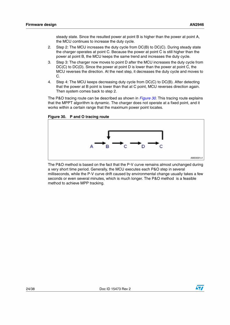
The P&O tracing route can be described as shown in Figure 30. This tracing route explains that the MPPT algorithm is dynamic. The charger does not operate at a fixed point, and it works within a certain range that the maximum power point locates.
Figure 30. P and O tracing route
The P&O method is based on the fact that the P-V curve remains almost unchanged during a very short time period. Generally, the MCU executes each P&O step in several milliseconds, while the P-V curve drift caused by environmental change usually takes a few seconds or even several minutes, which is much longer. The P&O method is a feasible method to achieve MPP tracking.

AN2946 Firmware design
Doc ID 15473 Rev 2 25/38
4.2.2 Battery charging management
Figure 31. Three-stage charging routine
The battery charging flowchart is illustrated in Figure 31. The MPPT algorithm is involved in stage 1 and stage 2 charging. The stage 1 is a current constraint. In stage 3, the charger keeps changing the charging current to maintain a constant charging voltage.
The MPPT algorithm illustrated in Figure 32, simplifies the conventional P&O method. Since battery voltage cannot drastically change in a short period, the maximum power point must lie on the maximum current point. This allows the MCU to compare current instead of a power comparison which is more complex for an embedded system.
Figure 32. MPPT flowchart
Firmware design AN2946
26/38 Doc ID 15473 Rev 2
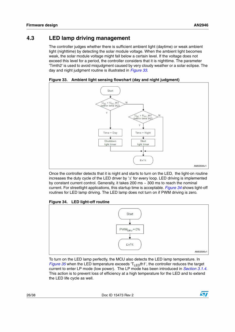
4.3 LED lamp driving managementThe controller judges whether there is sufficient ambient light (daytime) or weak ambient light (nighttime) by detecting the solar module voltage. When the ambient light becomes weak, the solar module voltage might fall below a certain level. If the voltage does not exceed this level for a period, the controller considers that it is nighttime. The parameter 'Timth2' is used to avoid misjudgment caused by very cloudy weather or a solar eclipse. The day and night judgment routine is illustrated in Figure 33.
Figure 33. Ambient light sensing flowchart (day and night judgment)
Once the controller detects that it is night and starts to turn on the LED, the light-on routine increases the duty cycle of the LED driver by 'Δ' for every loop. LED driving is implemented by constant current control. Generally, it takes 200 ms ~ 300 ms to reach the nominal current. For streetlight applications, this startup time is acceptable. Figure 34 shows light-off routines for LED lamp driving. The LED lamp does not turn on if PWM driving is zero.
Figure 34. LED light-off routine
To turn on the LED lamp perfectly, the MCU also detects the LED lamp temperature. In Figure 35 when the LED temperature exceeds 'TLEDth1', the controller reduces the target current to enter LP mode (low power). The LP mode has been introduced in Section 3.1.4. This action is to prevent loss of efficiency at a high temperature for the LED and to extend the LED life cycle as well.

AN2946 Firmware design
Doc ID 15473 Rev 2 27/38
Figure 35. LED light-on routine
4.4 System monitoring managementThe system monitoring routine is executed at the beginning of every loop. It checks if voltage, current or temperature is abnormal or not. A corresponding protective action is implemented and 'ErrorFlag' is set if any error occurs. The controller maintains the protective action until 'ErrorFlag' is cleared by the system recovery routine. The flowchart is shown in Figure 36.
Figure 36. System monitoring flowchart

Firmware design AN2946
28/38 Doc ID 15473 Rev 2
In system monitoring management, LED_Fault IRQ is the only interrupt to trigger the MCU EXTI peripheral which is implemented by the hardware and firmware. In some abnormal situations, the primary current of LED driving might rise radically, and then the pulse-shaped LED_Fault signal is generated by a comparator. Several rising edges of this interrupt in EXTI tell the controller to stop driving the LED and wait for system recovery. The flowchart is shown in Figure 37.
Figure 37. LED_fault IRQ flowchart
A complete monitoring system should include a self-recovery function. Every second, which is defined by 'Timth1', the controller tries to recover system errors by clearing 'ErrorFlag'. This enables all the error functions paused at the last system monitoring routine to run again. The system self-recovery flowchart is shown in Figure 38.
Figure 38. System self-recovery flowchart
To prevent battery power backflow through the charger, KCHG should be turned off when charging current is very low. In normal conditions, KCHG is turned on to reduce power loss in its body diode. The flowchart of anti-backflow for the battery charger is shown in Figure 39.

AN2946 Firmware design
Doc ID 15473 Rev 2 29/38
Figure 39. Anti-backflow for battery charging flowchart

Overview of demonstration board AN2946
30/38 Doc ID 15473 Rev 2
5 Overview of demonstration board
5.1 Application schematic
Figure 40. Schematic

AN2946 Overview of demonstration board
Doc ID 15473 Rev 2 31/38
5.2 Application board
Figure 41. Top view of demonstration board
Figure 42. Bottom view of demonstration board

Overview of demonstration board AN2946
32/38 Doc ID 15473 Rev 2
5.3 Bill of material
Table 5. BOM
Name Value Rated Type
B1 One way 6x6 mm (SMD), 4.3 mm(H), tactile switch OMRON
C1, C6 1 µF (1210), 100 V, ceramic capacitor
C2, C3, C12, C14, C24, C36, C39, C41, C42, C43, C46, C48, C49, C50, C51, C52, C56, C57, C58, C60,
C62, C65, C66, C67, C68, C77, C79
100 nF (0603), 50 V, ceramic capacitor
C4, C5, C13 470 µF 63 V, Al-cap electrolytic capacitor Rubycon
C7, C8, C35, C38, C45, C53, C73, C74
1 µF (0805), 25 V, ceramic capacitor
C9, C22, C34, C44, C75, C76, C80
22 µF 50 V, Al-cap electrolytic capacitor Rubycon
C10, C11, C25, C26 220 pF (0805), 50 V, ceramic capacitor
C15, C20 1 µF (1206), 50 V, ceramic capacitor
C17 560 pF (0603), 50 V, ceramic capacitor
C18, C19, C30, C33 220 µF 50 V, Al-cap electrolytic capacitor Rubycon
C23, C59, C61, C63, C69, C70, C71, C72,
330 nF (0805), 50 V, ceramic capacitor
C27, C29, C32, C64, C83 100 pF (0603), 50 V, ceramic capacitor
C28 220 pF (0603), 250 V, ceramic capacitor
C47 10 µF (3528-21), 16 V, tantalum VISHAY
C54, C55 20 pF (0603), 50 V, ceramic capacitor
CN1 20-way box header (Right angle mounting), JTAG connector Tyco electronics
D1, D11, D13, D17, D18, D19, D20, D21, D22, D23, D24, D25, D26, D27, D28, D29, D30, D31, D32, D33,
D34, D35, D36, D37
BAT46JFILM (SOD323), small signal Schottky diode STMicroelectronics
D2, D3, D12 15 V (SOD 80C), Zener diode
D4, D10 STPS20H100CFP (TO-220FPAB), power Schottky rectifier STMicroelectronics
D5, D9 SMAJ24A-TR(SMA or DO-214AC), 24V 400W
TransilTM (TVS)STMicroelectronics
D7 3.9 V (SOD 80C), Zener diode
D8 STPS1H100A(SMA or DO-214AC), power Schottky
rectifierSTMicroelectronics
D14 STPS2045CFP (TO-220FPAB), power Schottky rectifier STMicroelectronics

AN2946 Overview of demonstration board
Doc ID 15473 Rev 2 33/38
D16 STPS1L60A(SMA or DO-214AC), power Schottky
rectifierSTMicroelectronics
F1 10 A(2.54 x 7.2 mm, axial lead), 251 series
fuseLittelfuse®
JP1 (see Table 6) 0.64x0.64 mm, 2 way 2.54 mm pitch, Pin strip header 3M
L2 (see Table 6) 39 µH Inductor BOBITRANS
L5, L6 600 Ω @ 100 MHz(0603), Chip ferrite bead, 25%, 200mA
max.MuRata
LD1, LD2, LD3, LD4 80 mcd, yellow (0603), LED VISHAY
LD5 45 mcd, red (3.0, diffused, radio lead), LED VISHAY
LD6 10 mcd, green (3.0, undiffused, radio lead), LED VISHAY
P1, P2, P3 Terminal block 2 Terminal, pitch 7.5 mm DEGSON®
P4, P5, P6 Header, 2 pin HDR1x2, pitch 2.54 mm
Q1 STP40NF10 (TO-220), N-channel MOSFET STMicroelectronics
Q2, Q4 STP75NF75FP (TO-220FP), N-channel MOSFET STMicroelectronics
Q3, Q5, Q6, Q7, Q11, Q12
MMBTA42 (SOT-23), NPN bipolar transistor STMicroelectronics
Q8, Q9, Q13, Q14 BC807 (SOT-23), PNP bipolar transistor
Q10 TYN616RG (TO-220AB), Triac STMicroelectronics
R1, R2, R3, R4, R9, R17, R18, R19, R20, R46, R47,
R550.1 Ω (1206), 1%, resistor
R5, R7, R10, R12, R15, R16, R22, R23, R24, R26,
R28, R31, R40, R53, R101
10 Ω (0805), 1%, resistor
R6, R13, R29 10 kΩ (0805), 5%, resistor
R8 0.2 Ω (Axial lead), cement, 2 W, resistor TOKEN®
R11, R45, R48, R49, R59, R60, R61, R62, R63, R64,
R65, R67, R69, R95, R97, R104, R105, R110, R111, R112, R113, R114, R117, R118, R119, R120, R121, R122, R123, R124,
R125
10 kΩ (0603), 5%, resistor
R14, R27, R50 1.2 kΩ (0805), 5%, resistor
R21, R70, R71, R72, R73, R74, R106
330 Ω (0603), 5%, resistor
R25 1.8 kΩ (0603), 5%, resistor
R30, R33, R54 33 mΩ (1210), 1%, resistor
Table 5. BOM (continued)
Name Value Rated Type

Overview of demonstration board AN2946
34/38 Doc ID 15473 Rev 2
R32, R88 NTC, 10 kΩ (0805), NTC resistor
R34, R107, R108, R116 1 kΩ (0603), 1%, resistor
R35 24 Ω (1206), 5%, resistor
R36, R41 10 kΩ (0603), 1%, resistor
R37 12 kΩ (0603), 1%, resistor
R38, R39 4.7 kΩ (0603), 5%, resistor
R102 560 Ω (1206), 5%, resistor
R43 9.1 kΩ (0603), 1%, resistor
R44, R89, R91, R93 3.3 kΩ (0603), 1%, resistor
R51 330 kΩ (0603), 5%, resistor
R52 120 Ω (0603), 5%, resistor
R56, R58, R96 47 kΩ (0603), 5%, resistor
R57 3.3 kΩ (0603), 5%, resistor
R66 1 MΩ (0603), 1%, resistor
R68 1.8 kΩ (0603), 1%, resistor
R75 150 kΩ (0805), 1%, resistor
R76, R78, R81, R84 10 kΩ (0805), 1%, resistor
R77, R80 82 kΩ (0805), 1%, resistor
R79, R82, R85, R86, R87, R90, R92, R94
10 Ω (0603), 5%, resistor
R83 39 kΩ (0805), 1%, resistor
R98, R99, R100, R103 1 kΩ (0603), 5%, resistor
R109, R115 20 kΩ (0603), 1%, resistor
S1 DIP Switch 4 Position DIP Switch
T1 (see Table 6) 33 µH EER25.5, transformer BOBITRANS
T2 (see Table 6) 1 mH Driver transformer BOBITRANS
U1, U5 LM258D (SO8 narrow), dual operational amplifiers STMicroelectronics
U2, U4, U8 TS391ILT (SO), single voltage comparator STMicroelectronics
U3, U9 TSC101AILT (SO), current sense IC STMicroelectronics
U6 L78L12ABD-TR (SO8 narrow), positive voltage regulator STMicroelectronics
U7 LM193D (SO8), dual voltage comparator STMicroelectronics
U10 STM32F101RXT6 (LQFP64), 32-bit microprocessor STMicroelectronics
U11 L4931ABD33-TR (SO8 narrow), linear regulator STMicroelectronics
X1 8 MHz (φ3x8) crystal oscillatorYuechung
International Corp.
Table 5. BOM (continued)
Name Value Rated Type
AN2946 Overview of demonstration board
Doc ID 15473 Rev 2 35/38
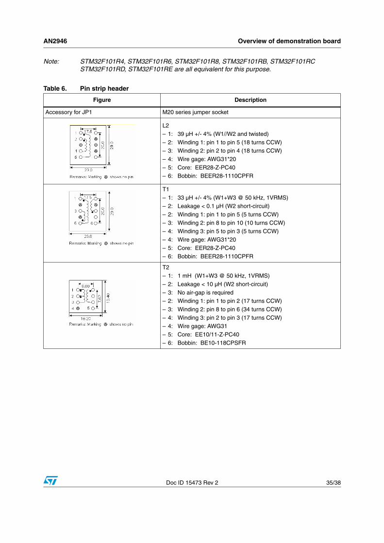
Note: STM32F101R4, STM32F101R6, STM32F101R8, STM32F101RB, STM32F101RC STM32F101RD, STM32F101RE are all equivalent for this purpose.
Table 6. Pin strip header
Figure Description
Accessory for JP1 M20 series jumper socket
L2
– 1: 39 µH +/- 4% (W1//W2 and twisted)
– 2: Winding 1: pin 1 to pin 5 (18 turns CCW)– 3: Winding 2: pin 2 to pin 4 (18 turns CCW)
– 4: Wire gage: AWG31*20
– 5: Core: EER28-Z-PC40– 6: Bobbin: BEER28-1110CPFR
T1
– 1: 33 µH +/- 4% (W1+W3 @ 50 kHz, 1VRMS)– 2: Leakage < 0.1 µH (W2 short-circuit)
– 2: Winding 1: pin 1 to pin 5 (5 turns CCW)
– 3: Winding 2: pin 8 to pin 10 (10 turns CCW)– 4: Winding 3: pin 5 to pin 3 (5 turns CCW)
– 4: Wire gage: AWG31*20
– 5: Core: EER28-Z-PC40– 6: Bobbin: BEER28-1110CPFR
T2– 1: 1 mH (W1+W3 @ 50 kHz, 1VRMS)
– 2: Leakage < 10 µH (W2 short-circuit)
– 3: No air-gap is required– 2: Winding 1: pin 1 to pin 2 (17 turns CCW)
– 3: Winding 2: pin 8 to pin 6 (34 turns CCW)
– 4: Winding 3: pin 2 to pin 3 (17 turns CCW)
– 4: Wire gage: AWG31– 5: Core: EE10/11-Z-PC40
– 6: Bobbin: BE10-118CPSFR

References AN2946
36/38 Doc ID 15473 Rev 2
6 References
1. "BAT46JFILM, Small signal Schottky diode" (datasheet)
2. "STPS20H100CFP, Power Schottky rectifier" (datasheet)
3. "STPS1L60A, power Schottky rectifier" (datasheet)
4. "STPS2045CFP, power Schottky rectifier" (datasheet)
5. "SMAJ24A-TR, 24 V 400 W TransilTM" (datasheet)
6. "STPS1H100A, power Schottky rectifier" (datasheet)
7. "MMBTA42, NPN bipolar transistor" (datasheet)
8. "STP40NF10, N-channel power MOSFET" (datasheet)
9. "STP60NF06FP, N-channel power MOSFET" (datasheet)
10. "STP75NF75FP, N-channel power MOSFET" (datasheet)
11. "TYN616RG, Triac" (datasheet)
12. "LM258D, Low power dual operational amplifiers" (datasheet)
13. "TS391ILT, Single voltage comparator" (datasheet)
14. "TSC101AILT, current sense IC" (datasheet)
15. "L78L12ABD, positive voltage regulator" (datasheet)
16. "STM32F101RXT6, 32-bit microcontroller" (datasheet)

AN2946 Revision history
Doc ID 15473 Rev 2 37/38
7 Revision history
Table 7. Document revision history
Date Revision Changes
16-Oct-2009 1 Initial release.
28-Sep-2010 2
– For easy mount and better operating life of demo-board, below type of connectors are changed.
1: P1: Solar panel connector2: P2: Battery connector
3: P3: LED lamp connector
– MCU reset switch is renamed as B1. – Battery use only 12VDC. Below figures are renew according to the
modification. – Figure 1, 6, 7, 9, 10, 11, 12, 13, 14, 18, 40, 41, 42 changed
– Table 5 updated

AN2946
38/38 Doc ID 15473 Rev 2
Please Read Carefully:
Information in this document is provided solely in connection with ST products. STMicroelectronics NV and its subsidiaries (“ST”) reserve theright to make changes, corrections, modifications or improvements, to this document, and the products and services described herein at anytime, without notice.
All ST products are sold pursuant to ST’s terms and conditions of sale.
Purchasers are solely responsible for the choice, selection and use of the ST products and services described herein, and ST assumes noliability whatsoever relating to the choice, selection or use of the ST products and services described herein.
No license, express or implied, by estoppel or otherwise, to any intellectual property rights is granted under this document. If any part of thisdocument refers to any third party products or services it shall not be deemed a license grant by ST for the use of such third party productsor services, or any intellectual property contained therein or considered as a warranty covering the use in any manner whatsoever of suchthird party products or services or any intellectual property contained therein.
UNLESS OTHERWISE SET FORTH IN ST’S TERMS AND CONDITIONS OF SALE ST DISCLAIMS ANY EXPRESS OR IMPLIEDWARRANTY WITH RESPECT TO THE USE AND/OR SALE OF ST PRODUCTS INCLUDING WITHOUT LIMITATION IMPLIEDWARRANTIES OF MERCHANTABILITY, FITNESS FOR A PARTICULAR PURPOSE (AND THEIR EQUIVALENTS UNDER THE LAWSOF ANY JURISDICTION), OR INFRINGEMENT OF ANY PATENT, COPYRIGHT OR OTHER INTELLECTUAL PROPERTY RIGHT.
UNLESS EXPRESSLY APPROVED IN WRITING BY AN AUTHORIZED ST REPRESENTATIVE, ST PRODUCTS ARE NOTRECOMMENDED, AUTHORIZED OR WARRANTED FOR USE IN MILITARY, AIR CRAFT, SPACE, LIFE SAVING, OR LIFE SUSTAININGAPPLICATIONS, NOR IN PRODUCTS OR SYSTEMS WHERE FAILURE OR MALFUNCTION MAY RESULT IN PERSONAL INJURY,DEATH, OR SEVERE PROPERTY OR ENVIRONMENTAL DAMAGE. ST PRODUCTS WHICH ARE NOT SPECIFIED AS "AUTOMOTIVEGRADE" MAY ONLY BE USED IN AUTOMOTIVE APPLICATIONS AT USER’S OWN RISK.
Resale of ST products with provisions different from the statements and/or technical features set forth in this document shall immediately voidany warranty granted by ST for the ST product or service described herein and shall not create or extend in any manner whatsoever, anyliability of ST.
ST and the ST logo are trademarks or registered trademarks of ST in various countries.
Information in this document supersedes and replaces all information previously supplied.
The ST logo is a registered trademark of STMicroelectronics. All other names are the property of their respective owners.
© 2010 STMicroelectronics - All rights reserved
STMicroelectronics group of companies
Australia - Belgium - Brazil - Canada - China - Czech Republic - Finland - France - Germany - Hong Kong - India - Israel - Italy - Japan - Malaysia - Malta - Morocco - Philippines - Singapore - Spain - Sweden - Switzerland - United Kingdom - United States of America
www.st.com