snis125d – march 2004– revised … lm71-q1 snis125d – march 2004– revised march 2013...
TRANSCRIPT
Temperature
Sensor
Circuitry
Control
Logic
Temperature
Register
Manufacturer's
ID Register
Three-Wire
Serial Interface
14-Bit
Delta-Sigma
A/D Converter
SI/O
SC
2.65V to 5.5V
LM71
CS
An IMPORTANT NOTICE at the end of this data sheet addresses availability, warranty, changes, use in safety-critical applications,intellectual property matters and other important disclaimers. PRODUCTION DATA.
LM71, LM71-Q1SNIS125E –MARCH 2004–REVISED AUGUST 2018
LM71/LM71-Q1 SPI/MICROWIRE 13-Bit Plus Sign Temperature Sensor
1
1 Features1• LM71Q is AEC-Q100 Grade 0 Qualified and is
Manufactured on an Automotive Grade Flow• 5-Pin SOT-23 Package or 6-Pin No-Pull-Back
WSON Package• Operates Over a Full −40°C to +150°C Range• SPI and MICROWIRE Bus Interface• Key Specifications:
– Supply Voltage: 2.65V to 5.5V– Supply Current
– Operating: 300 µA (typ)– 550 µA (max)
– Temperature Accuracy– −10°C to +65°C: ±1.5°C (max)– −40°C to 150°C: +3/− 2°C (max)
– Temperature Resolution: 31.25 m°C
2 Applications• System Thermal Management• Personal Computers• Portable Electronic Devices• Disk Drives• Office Electronics• Electronic Test Equipment• Vending Machines• Automotive
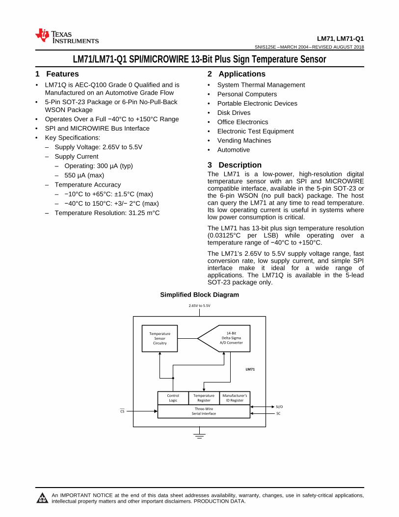
3 DescriptionThe LM71 is a low-power, high-resolution digitaltemperature sensor with an SPI and MICROWIREcompatible interface, available in the 5-pin SOT-23 orthe 6-pin WSON (no pull back) package. The hostcan query the LM71 at any time to read temperature.Its low operating current is useful in systems wherelow power consumption is critical.
The LM71 has 13-bit plus sign temperature resolution(0.03125°C per LSB) while operating over atemperature range of −40°C to +150°C.
The LM71’s 2.65V to 5.5V supply voltage range, fastconversion rate, low supply current, and simple SPIinterface make it ideal for a wide range ofapplications. The LM71Q is available in the 5-leadSOT-23 package only.
Simplified Block Diagram
LM71
1
2
3 4
5CS
GND
SI/O SC
V+
LM71
1
2
3 4
6
CS
GND
SI/O
SC V+
5 GND
2
LM71, LM71-Q1SNIS125E –MARCH 2004–REVISED AUGUST 2018 www.ti.com
Product Folder Links: LM71 LM71-Q1
Submit Documentation Feedback Copyright © 2004–2018, Texas Instruments Incorporated
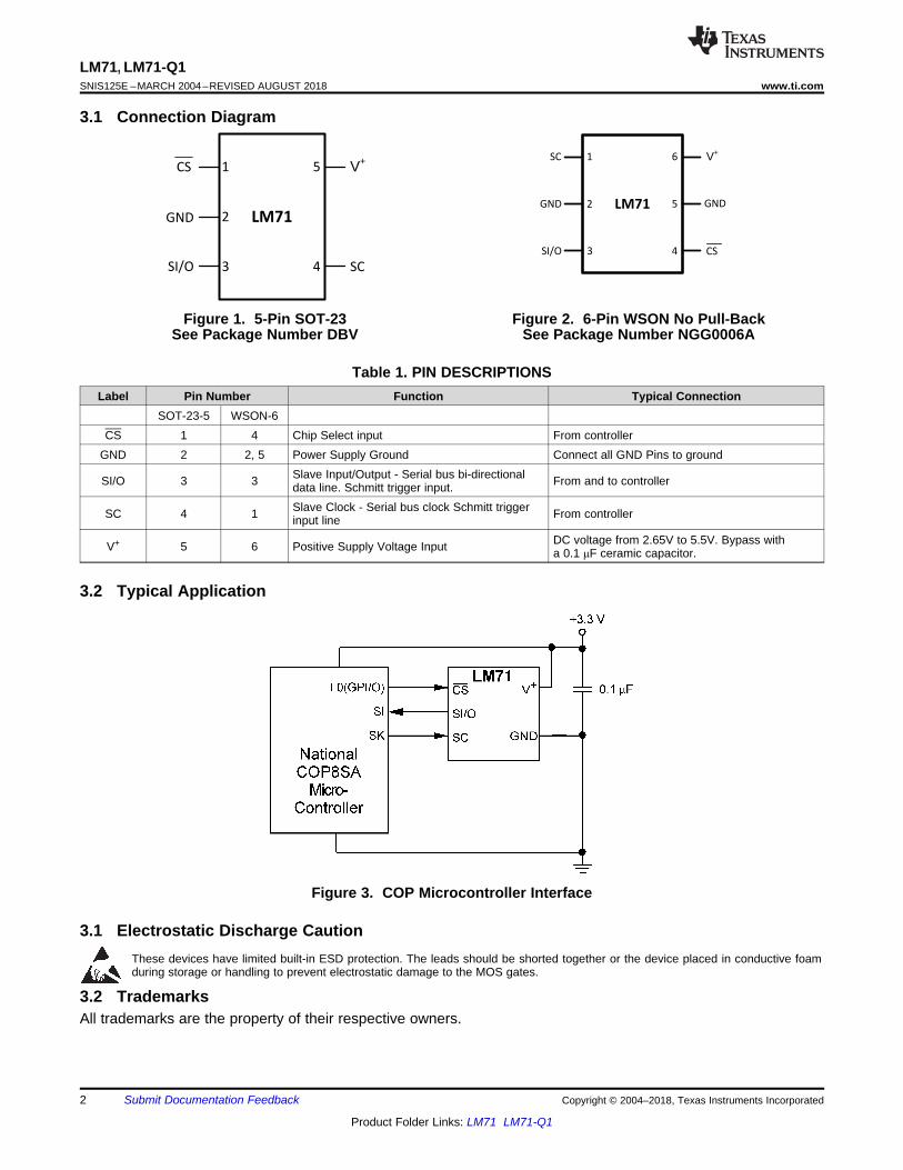
3.1 Connection Diagram
Figure 1. 5-Pin SOT-23See Package Number DBV
Figure 2. 6-Pin WSON No Pull-BackSee Package Number NGG0006A
Table 1. PIN DESCRIPTIONSLabel Pin Number Function Typical Connection
SOT-23-5 WSON-6CS 1 4 Chip Select input From controller
GND 2 2, 5 Power Supply Ground Connect all GND Pins to ground
SI/O 3 3 Slave Input/Output - Serial bus bi-directionaldata line. Schmitt trigger input. From and to controller
SC 4 1 Slave Clock - Serial bus clock Schmitt triggerinput line From controller
V+ 5 6 Positive Supply Voltage Input DC voltage from 2.65V to 5.5V. Bypass witha 0.1 μF ceramic capacitor.
3.2 Typical Application
Figure 3. COP Microcontroller Interface
3.1 Electrostatic Discharge CautionThese devices have limited built-in ESD protection. The leads should be shorted together or the device placed in conductive foamduring storage or handling to prevent electrostatic damage to the MOS gates.
3.2 TrademarksAll trademarks are the property of their respective owners.
3
LM71, LM71-Q1www.ti.com SNIS125E –MARCH 2004–REVISED AUGUST 2018
Product Folder Links: LM71 LM71-Q1
Submit Documentation FeedbackCopyright © 2004–2018, Texas Instruments Incorporated
(1) Absolute Maximum Ratings indicate limits beyond which damage to the device may occur. DC and AC electrical specifications do notapply when operating the device beyond its rated operating conditions.
(2) When the input voltage (VI) at any pin exceeds the power supplies (VI < GND or VI > +VS) the current at that pin should be limited to 5mA.
(3) Human body model, 100 pF discharged through a 1.5 kΩ resistor. Machine model, 200 pF discharged directly into each pin.
4 Absolute Maximum Ratings (1)
Supply Voltage −0.3V to 6.0VVoltage at any Pin −0.3V to V+ + 0.3VInput Current at any Pin (2) 5 mAStorage Temperature −65°C to +150°C
Soldering Information, Lead TemperatureSOT-23-5 Package
Vapor Phase (60 seconds) 215°CInfrared (15 seconds) 220°C
WSON-6 Package Infrared (5 seconds) 215°C
ESD Susceptibility (3) Human Body Model 2000VMachine Model 200V
(1) The life expectancy of the LM71 will be reduced when operating at elevated temperatures. LM71 θJA (thermal resistance, junction-to-ambient) when attached to a printed circuit board with 2 oz. foil is summarized in the table below:
5 Operating RatingsSpecified Temperature Range (1) (TMIN to TMAX) LM71CIMF, LM71CISD, LM71QCIMF −40°C to +150°CSupply Voltage Range (+VS) LM71CIMF, LM71CISD, LM71QCIMF +2.65V to +5.5V
4
LM71, LM71-Q1SNIS125E –MARCH 2004–REVISED AUGUST 2018 www.ti.com
Product Folder Links: LM71 LM71-Q1
Submit Documentation Feedback Copyright © 2004–2018, Texas Instruments Incorporated
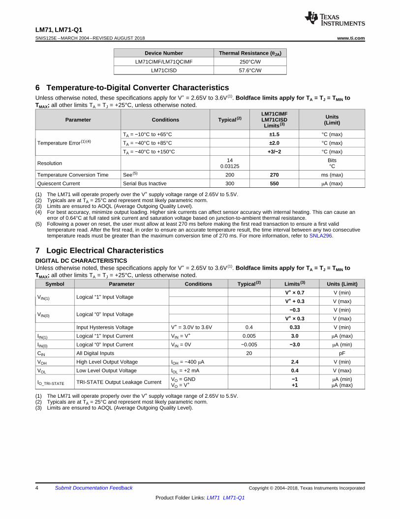
Device Number Thermal Resistance (θJA)LM71CIMF/LM71QCIMF 250°C/W
LM71CISD 57.6°C/W
(1) The LM71 will operate properly over the V+ supply voltage range of 2.65V to 5.5V.(2) Typicals are at TA = 25°C and represent most likely parametric norm.(3) Limits are ensured to AOQL (Average Outgoing Quality Level).(4) For best accuracy, minimize output loading. Higher sink currents can affect sensor accuracy with internal heating. This can cause an
error of 0.64°C at full rated sink current and saturation voltage based on junction-to-ambient thermal resistance.(5) Following a power on reset, the user must allow at least 270 ms before making the first read transaction to ensure a first valid
temperature read. After the first read, in order to ensure an accurate temperature result, the time interval between any two consecutivetemperature reads must be greater than the maximum conversion time of 270 ms. For more information, refer to SNLA296.
6 Temperature-to-Digital Converter CharacteristicsUnless otherwise noted, these specifications apply for V+ = 2.65V to 3.6V (1). Boldface limits apply for TA = TJ = TMIN toTMAX; all other limits TA = TJ = +25°C, unless otherwise noted.
Parameter Conditions Typical (2)LM71CIMFLM71CISDLimits (3)
Units(Limit)
Temperature Error (1) (4)
TA = −10°C to +65°C ±1.5 °C (max)TA = −40°C to +85°C ±2.0 °C (max)TA = −40°C to +150°C +3/−2 °C (max)
Resolution 140.03125
Bits°C
Temperature Conversion Time See (5) 200 270 ms (max)Quiescent Current Serial Bus Inactive 300 550 μA (max)
(1) The LM71 will operate properly over the V+ supply voltage range of 2.65V to 5.5V.(2) Typicals are at TA = 25°C and represent most likely parametric norm.(3) Limits are ensured to AOQL (Average Outgoing Quality Level).
7 Logic Electrical CharacteristicsDIGITAL DC CHARACTERISTICSUnless otherwise noted, these specifications apply for V+ = 2.65V to 3.6V (1). Boldface limits apply for TA = TJ = TMIN toTMAX; all other limits TA = TJ = +25°C, unless otherwise noted.
Symbol Parameter Conditions Typical (2) Limits (3) Units (Limit)
VIN(1) Logical “1” Input VoltageV+ × 0.7 V (min)V+ + 0.3 V (max)
VIN(0) Logical “0” Input Voltage−0.3 V (min)
V+ × 0.3 V (max)Input Hysteresis Voltage V+ = 3.0V to 3.6V 0.4 0.33 V (min)
IIN(1) Logical “1” Input Current VIN = V+ 0.005 3.0 μA (max)IIN(0) Logical “0” Input Current VIN = 0V −0.005 −3.0 μA (min)CIN All Digital Inputs 20 pFVOH High Level Output Voltage IOH = −400 μA 2.4 V (min)VOL Low Level Output Voltage IOL = +2 mA 0.4 V (max)
IO_TRI-STATE TRI-STATE Output Leakage Current VO = GNDVO = V+
−1+1
μA (min)μA (max)

SC
SO
CS
t5
30%
70%
70%
SC70%
30%
70%
30%
70%
30%
SO
CS
t3
t2t4 t4
70%
30%
tf tr
30%
70%
5
LM71, LM71-Q1www.ti.com SNIS125E –MARCH 2004–REVISED AUGUST 2018
Product Folder Links: LM71 LM71-Q1
Submit Documentation FeedbackCopyright © 2004–2018, Texas Instruments Incorporated
(1) The LM71 will operate properly over the V+ supply voltage range of 2.65V to 5.5V.(2) Typicals are at TA = 25°C and represent most likely parametric norm.(3) Limits are ensured to AOQL (Average Outgoing Quality Level).
SERIAL BUS DIGITAL SWITCHING CHARACTERISTICSUnless otherwise noted, these specifications apply for V+ = 2.65V to 3.6V (1); CL (load capacitance) on output lines = 100 pFunless otherwise specified. Boldface limits apply for TA = TJ = TMIN to TMAX; all other limits TA = TJ = +25°C, unlessotherwise noted.
Symbol Parameter Conditions Typical (2) Limits (3) Units(Limit)
t1 SC (Clock) Period 0.16DC
μs (min)(max)
t2 CS Low to SC (Clock) High Set-Up Time 100 ns (min)t3 CS Low to Data Out (SO) Delay 70 ns (max)t4 SC (Clock) Low to Data Out (SO) Delay 70 ns (max)t5 CS High to Data Out (SO) TRI-STATE 200 ns (max)t6 SC (Clock) High to Data In (SI) Hold Time 50 ns (min)t7 Data In (SI) Set-Up Time to SC (Clock) High 30 ns (min)tr SC (Clock) Rise Time 100 ns (max)tf SC (Clock) Fall Time 100 ns (max)
Figure 4. Data Output Timing Diagram
Figure 5. TRI-STATE Data Output Timing Diagram
SC
SI
CS
t6
30%
70%
70%
30%
t7
6
LM71, LM71-Q1SNIS125E –MARCH 2004–REVISED AUGUST 2018 www.ti.com
Product Folder Links: LM71 LM71-Q1
Submit Documentation Feedback Copyright © 2004–2018, Texas Instruments Incorporated
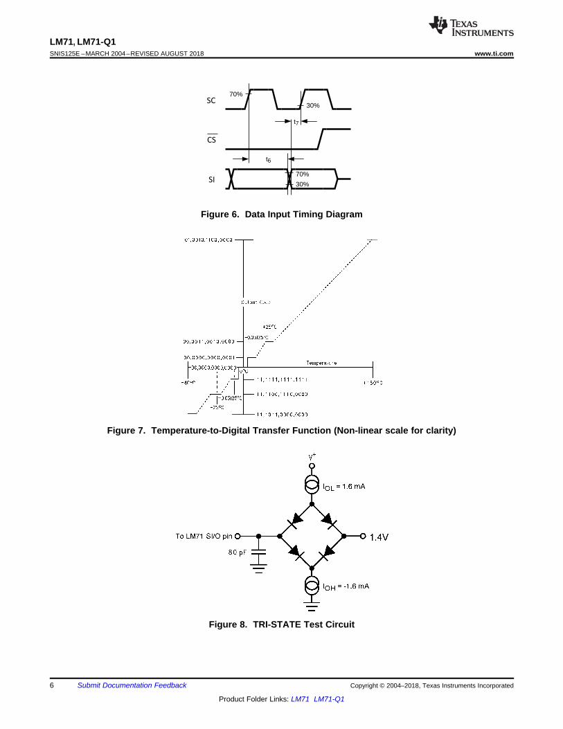
Figure 6. Data Input Timing Diagram
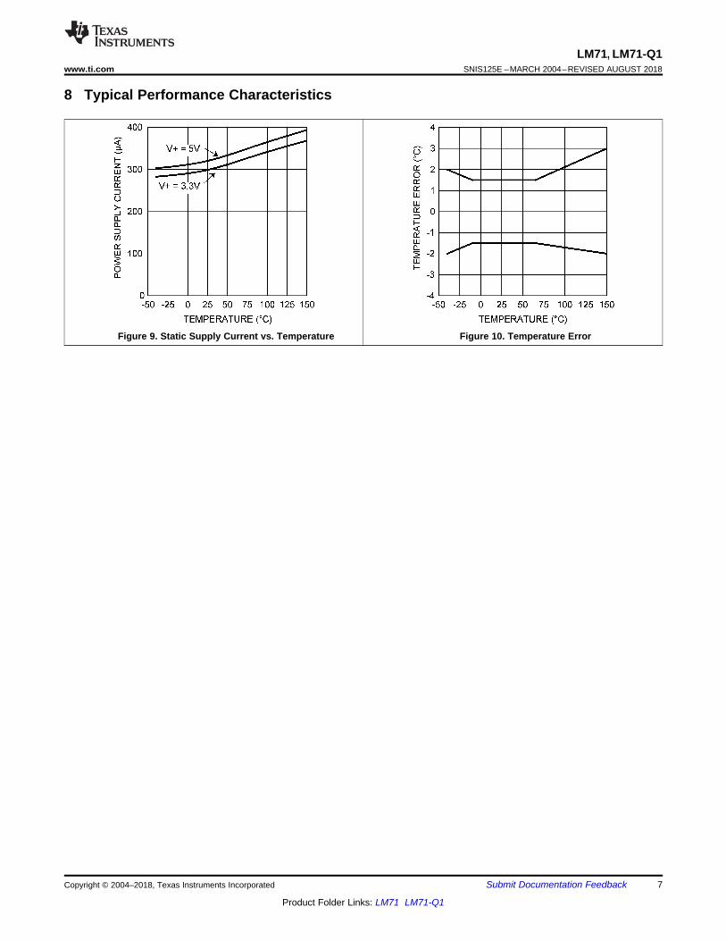
Figure 7. Temperature-to-Digital Transfer Function (Non-linear scale for clarity)
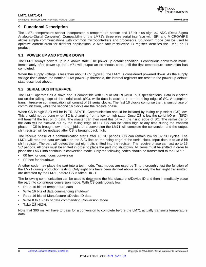
Figure 8. TRI-STATE Test Circuit
7
LM71, LM71-Q1www.ti.com SNIS125E –MARCH 2004–REVISED AUGUST 2018
Product Folder Links: LM71 LM71-Q1
Submit Documentation FeedbackCopyright © 2004–2018, Texas Instruments Incorporated
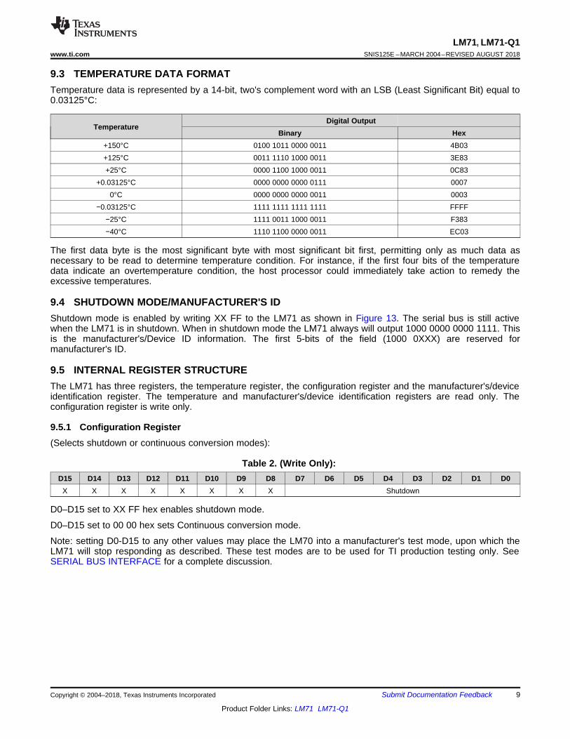
8 Typical Performance Characteristics
Figure 9. Static Supply Current vs. Temperature Figure 10. Temperature Error
8
LM71, LM71-Q1SNIS125E –MARCH 2004–REVISED AUGUST 2018 www.ti.com
Product Folder Links: LM71 LM71-Q1
Submit Documentation Feedback Copyright © 2004–2018, Texas Instruments Incorporated
9 Functional DescriptionThe LM71 temperature sensor incorporates a temperature sensor and 13-bit plus sign ΔΣ ADC (Delta-SigmaAnalog-to-Digital Converter). Compatibility of the LM71's three wire serial interface with SPI and MICROWIREallows simple communications with common microcontrollers and processors. Shutdown mode can be used tooptimize current drain for different applications. A Manufacture's/Device ID register identifies the LM71 as TIproduct.
9.1 POWER UP AND POWER DOWNThe LM71 always powers up in a known state. The power up default condition is continuous conversion mode.Immediately after power up the LM71 will output an erroneous code until the first temperature conversion hascompleted.
When the supply voltage is less than about 1.6V (typical), the LM71 is considered powered down. As the supplyvoltage rises above the nominal 1.6V power up threshold, the internal registers are reset to the power up defaultstate described above.
9.2 SERIAL BUS INTERFACEThe LM71 operates as a slave and is compatible with SPI or MICROWIRE bus specifications. Data is clockedout on the falling edge of the serial clock (SC), while data is clocked in on the rising edge of SC. A completetransmit/receive communication will consist of 32 serial clocks. The first 16 clocks comprise the transmit phase ofcommunication, while the second 16 clocks are the receive phase.
When CS is high SI/O will be in TRI-STATE. Communication should be initiated by taking chip select (CS) low.This should not be done when SC is changing from a low to high state. Once CS is low the serial I/O pin (SI/O)will transmit the first bit of data. The master can then read this bit with the rising edge of SC. The remainder ofthe data will be clocked out by the falling edge of SC. CS can be taken high at any time during the transmitphase. If CS is brought low in the middle of a conversion the LM71 will complete the conversion and the outputshift register will be updated after CS is brought back high.
The receive phase of a communication starts after 16 SC periods. CS can remain low for 32 SC cycles. TheLM71 will read the data available on the SI/O line on the rising edge of the serial clock. Input data is to an 8-bitshift register. The part will detect the last eight bits shifted into the register. The receive phase can last up to 16SC periods. All ones must be shifted in order to place the part into shutdown. All zeros must be shifted in order toplace the LM71 into continuous conversion mode. Only the following codes should be transmitted to the LM71:• 00 hex for continuous conversion• FF hex for shutdown
Another code may place the part into a test mode. Test modes are used by TI to thoroughly test the function ofthe LM71 during production testing. Only eight bits have been defined above since only the last eight transmittedare detected by the LM71, before CS is taken HIGH.
The following communication can be used to determine the Manufacturer's/Device ID and then immediately placethe part into continuous conversion mode. With CS continuously low:• Read 16 bits of temperature data• Write 16 bits of data commanding shutdown• Read 16 bits of Manufacture's/Device ID data• Write 8 to 16 bits of data commanding Conversion Mode• Take CS HIGH.
Note that 300 ms will have to pass for a conversion to complete before the LM71 actually transmits temperaturedata.
9
LM71, LM71-Q1www.ti.com SNIS125E –MARCH 2004–REVISED AUGUST 2018
Product Folder Links: LM71 LM71-Q1
Submit Documentation FeedbackCopyright © 2004–2018, Texas Instruments Incorporated
9.3 TEMPERATURE DATA FORMATTemperature data is represented by a 14-bit, two's complement word with an LSB (Least Significant Bit) equal to0.03125°C:
TemperatureDigital Output
Binary Hex+150°C 0100 1011 0000 0011 4B03+125°C 0011 1110 1000 0011 3E83+25°C 0000 1100 1000 0011 0C83
+0.03125°C 0000 0000 0000 0111 00070°C 0000 0000 0000 0011 0003
−0.03125°C 1111 1111 1111 1111 FFFF−25°C 1111 0011 1000 0011 F383−40°C 1110 1100 0000 0011 EC03
The first data byte is the most significant byte with most significant bit first, permitting only as much data asnecessary to be read to determine temperature condition. For instance, if the first four bits of the temperaturedata indicate an overtemperature condition, the host processor could immediately take action to remedy theexcessive temperatures.
9.4 SHUTDOWN MODE/MANUFACTURER'S IDShutdown mode is enabled by writing XX FF to the LM71 as shown in Figure 13. The serial bus is still activewhen the LM71 is in shutdown. When in shutdown mode the LM71 always will output 1000 0000 0000 1111. Thisis the manufacturer's/Device ID information. The first 5-bits of the field (1000 0XXX) are reserved formanufacturer's ID.
9.5 INTERNAL REGISTER STRUCTUREThe LM71 has three registers, the temperature register, the configuration register and the manufacturer's/deviceidentification register. The temperature and manufacturer's/device identification registers are read only. Theconfiguration register is write only.
9.5.1 Configuration Register(Selects shutdown or continuous conversion modes):
Table 2. (Write Only):D15 D14 D13 D12 D11 D10 D9 D8 D7 D6 D5 D4 D3 D2 D1 D0
X X X X X X X X Shutdown
D0–D15 set to XX FF hex enables shutdown mode.
D0–D15 set to 00 00 hex sets Continuous conversion mode.
Note: setting D0-D15 to any other values may place the LM70 into a manufacturer's test mode, upon which theLM71 will stop responding as described. These test modes are to be used for TI production testing only. SeeSERIAL BUS INTERFACE for a complete discussion.
10
LM71, LM71-Q1SNIS125E –MARCH 2004–REVISED AUGUST 2018 www.ti.com
Product Folder Links: LM71 LM71-Q1
Submit Documentation Feedback Copyright © 2004–2018, Texas Instruments Incorporated
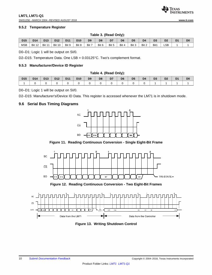
9.5.2 Temperature Register
Table 3. (Read Only):D15 D14 D13 D12 D11 D10 D9 D8 D7 D6 D5 D4 D3 D2 D1 D0MSB Bit 12 Bit 11 Bit 10 Bit 9 Bit 8 Bit 7 Bit 6 Bit 5 Bit 4 Bit 3 Bit 2 Bit1 LSB 1 1
D0–D1: Logic 1 will be output on SI/0.
D2–D15: Temperature Data. One LSB = 0.03125°C. Two's complement format.
9.5.3 Manufacturer/Device ID Register
Table 4. (Read Only):D15 D14 D13 D12 D11 D10 D9 D8 D7 D6 D5 D4 D3 D2 D1 D0
1 0 0 0 0 0 0 0 0 0 0 0 1 1 1 1
D0–D1: Logic 1 will be output on SI/0.
D2–D15: Manufacturer's/Device ID Data. This register is accessed whenever the LM71 is in shutdown mode.
9.6 Serial Bus Timing Diagrams
Figure 11. Reading Continuous Conversion - Single Eight-Bit Frame
Figure 12. Reading Continuous Conversion - Two Eight-Bit Frames
Figure 13. Writing Shutdown Control
11
LM71, LM71-Q1www.ti.com SNIS125E –MARCH 2004–REVISED AUGUST 2018
Product Folder Links: LM71 LM71-Q1
Submit Documentation FeedbackCopyright © 2004–2018, Texas Instruments Incorporated
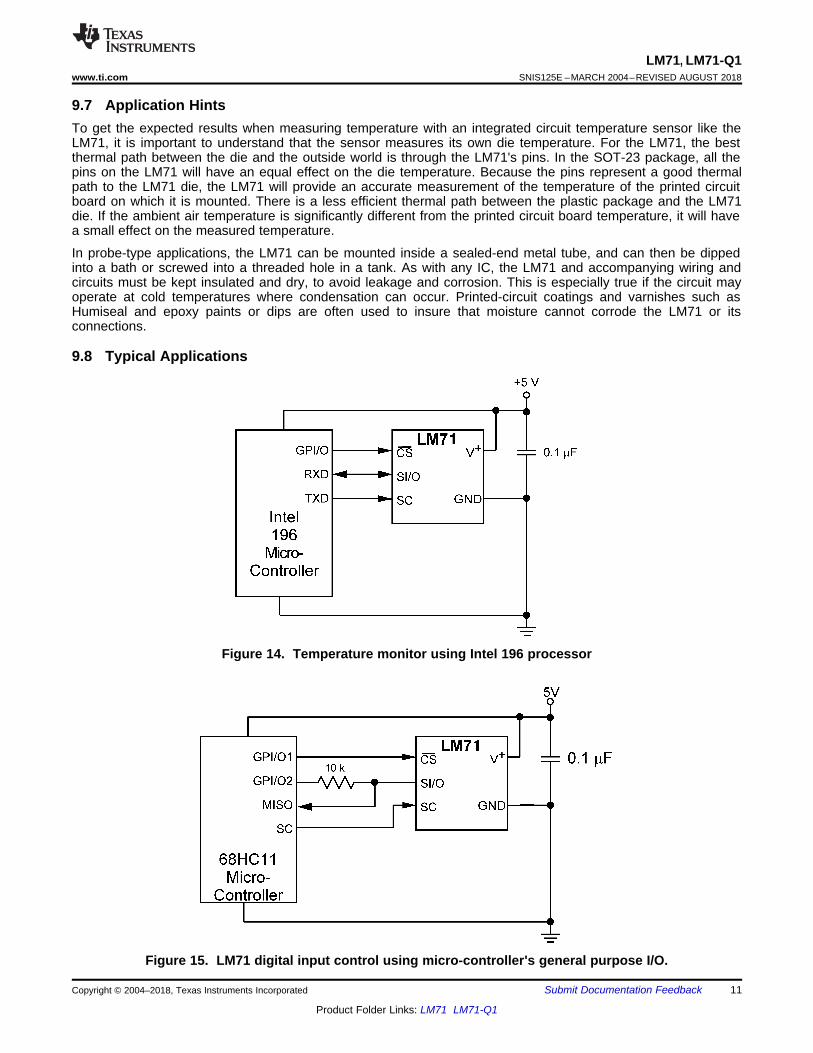
9.7 Application HintsTo get the expected results when measuring temperature with an integrated circuit temperature sensor like theLM71, it is important to understand that the sensor measures its own die temperature. For the LM71, the bestthermal path between the die and the outside world is through the LM71's pins. In the SOT-23 package, all thepins on the LM71 will have an equal effect on the die temperature. Because the pins represent a good thermalpath to the LM71 die, the LM71 will provide an accurate measurement of the temperature of the printed circuitboard on which it is mounted. There is a less efficient thermal path between the plastic package and the LM71die. If the ambient air temperature is significantly different from the printed circuit board temperature, it will havea small effect on the measured temperature.
In probe-type applications, the LM71 can be mounted inside a sealed-end metal tube, and can then be dippedinto a bath or screwed into a threaded hole in a tank. As with any IC, the LM71 and accompanying wiring andcircuits must be kept insulated and dry, to avoid leakage and corrosion. This is especially true if the circuit mayoperate at cold temperatures where condensation can occur. Printed-circuit coatings and varnishes such asHumiseal and epoxy paints or dips are often used to insure that moisture cannot corrode the LM71 or itsconnections.
9.8 Typical Applications
Figure 14. Temperature monitor using Intel 196 processor
Figure 15. LM71 digital input control using micro-controller's general purpose I/O.
12
LM71, LM71-Q1SNIS125E –MARCH 2004–REVISED AUGUST 2018 www.ti.com
Product Folder Links: LM71 LM71-Q1
Submit Documentation Feedback Copyright © 2004–2018, Texas Instruments Incorporated
10 Revision HistoryNOTE: Page numbers for previous revisions may differ from page numbers in the current version.
Changes from Revision D (March 2013) to Revision E Page
• Added SNLA296 ulink to the temperature conversion time tablenote.................................................................................... 4
Changes from Revision C (March 2013) to Revision D Page
• Changed layout of National Semiconductor Data Sheet to TI format .................................................................................. 11
PACKAGE OPTION ADDENDUM
www.ti.com 18-Jul-2018
Addendum-Page 1
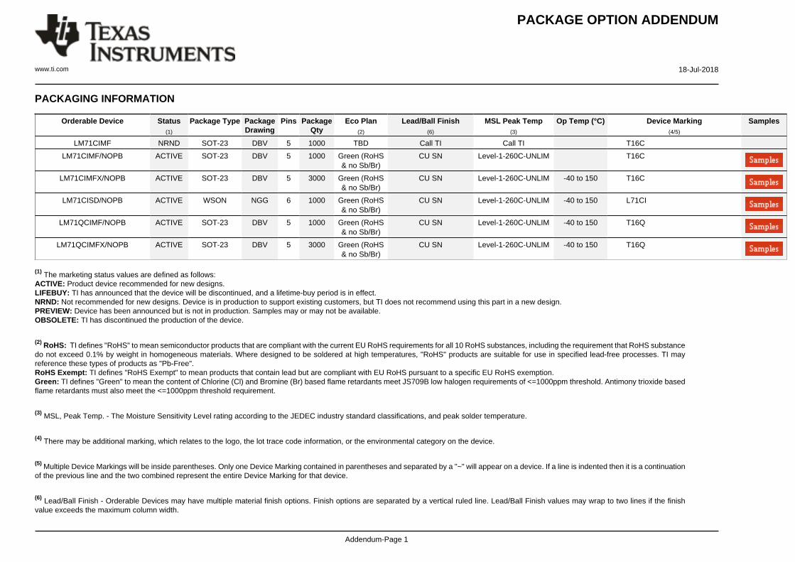
PACKAGING INFORMATION
Orderable Device Status(1)
Package Type PackageDrawing
Pins PackageQty
Eco Plan(2)
Lead/Ball Finish(6)
MSL Peak Temp(3)
Op Temp (°C) Device Marking(4/5)
Samples
LM71CIMF NRND SOT-23 DBV 5 1000 TBD Call TI Call TI T16C
LM71CIMF/NOPB ACTIVE SOT-23 DBV 5 1000 Green (RoHS& no Sb/Br)
CU SN Level-1-260C-UNLIM T16C
LM71CIMFX/NOPB ACTIVE SOT-23 DBV 5 3000 Green (RoHS& no Sb/Br)
CU SN Level-1-260C-UNLIM -40 to 150 T16C
LM71CISD/NOPB ACTIVE WSON NGG 6 1000 Green (RoHS& no Sb/Br)
CU SN Level-1-260C-UNLIM -40 to 150 L71CI
LM71QCIMF/NOPB ACTIVE SOT-23 DBV 5 1000 Green (RoHS& no Sb/Br)
CU SN Level-1-260C-UNLIM -40 to 150 T16Q
LM71QCIMFX/NOPB ACTIVE SOT-23 DBV 5 3000 Green (RoHS& no Sb/Br)
CU SN Level-1-260C-UNLIM -40 to 150 T16Q
(1) The marketing status values are defined as follows:ACTIVE: Product device recommended for new designs.LIFEBUY: TI has announced that the device will be discontinued, and a lifetime-buy period is in effect.NRND: Not recommended for new designs. Device is in production to support existing customers, but TI does not recommend using this part in a new design.PREVIEW: Device has been announced but is not in production. Samples may or may not be available.OBSOLETE: TI has discontinued the production of the device.
(2) RoHS: TI defines "RoHS" to mean semiconductor products that are compliant with the current EU RoHS requirements for all 10 RoHS substances, including the requirement that RoHS substancedo not exceed 0.1% by weight in homogeneous materials. Where designed to be soldered at high temperatures, "RoHS" products are suitable for use in specified lead-free processes. TI mayreference these types of products as "Pb-Free".RoHS Exempt: TI defines "RoHS Exempt" to mean products that contain lead but are compliant with EU RoHS pursuant to a specific EU RoHS exemption.Green: TI defines "Green" to mean the content of Chlorine (Cl) and Bromine (Br) based flame retardants meet JS709B low halogen requirements of <=1000ppm threshold. Antimony trioxide basedflame retardants must also meet the <=1000ppm threshold requirement.
(3) MSL, Peak Temp. - The Moisture Sensitivity Level rating according to the JEDEC industry standard classifications, and peak solder temperature.
(4) There may be additional marking, which relates to the logo, the lot trace code information, or the environmental category on the device.
(5) Multiple Device Markings will be inside parentheses. Only one Device Marking contained in parentheses and separated by a "~" will appear on a device. If a line is indented then it is a continuationof the previous line and the two combined represent the entire Device Marking for that device.
(6) Lead/Ball Finish - Orderable Devices may have multiple material finish options. Finish options are separated by a vertical ruled line. Lead/Ball Finish values may wrap to two lines if the finishvalue exceeds the maximum column width.
PACKAGE OPTION ADDENDUM
www.ti.com 18-Jul-2018
Addendum-Page 2
Important Information and Disclaimer:The information provided on this page represents TI's knowledge and belief as of the date that it is provided. TI bases its knowledge and belief on informationprovided by third parties, and makes no representation or warranty as to the accuracy of such information. Efforts are underway to better integrate information from third parties. TI has taken andcontinues to take reasonable steps to provide representative and accurate information but may not have conducted destructive testing or chemical analysis on incoming materials and chemicals.TI and TI suppliers consider certain information to be proprietary, and thus CAS numbers and other limited information may not be available for release.
In no event shall TI's liability arising out of such information exceed the total purchase price of the TI part(s) at issue in this document sold by TI to Customer on an annual basis.
OTHER QUALIFIED VERSIONS OF LM71, LM71-Q1 :
• Catalog: LM71
• Automotive: LM71-Q1
NOTE: Qualified Version Definitions:
• Catalog - TI's standard catalog product
• Automotive - Q100 devices qualified for high-reliability automotive applications targeting zero defects
TAPE AND REEL INFORMATION
*All dimensions are nominal
Device PackageType
PackageDrawing
Pins SPQ ReelDiameter
(mm)
ReelWidth
W1 (mm)
A0(mm)
B0(mm)
K0(mm)
P1(mm)
W(mm)
Pin1Quadrant
LM71CIMF SOT-23 DBV 5 1000 178.0 8.4 3.2 3.2 1.4 4.0 8.0 Q3
LM71CIMF/NOPB SOT-23 DBV 5 1000 178.0 8.4 3.2 3.2 1.4 4.0 8.0 Q3
LM71CIMFX/NOPB SOT-23 DBV 5 3000 178.0 8.4 3.2 3.2 1.4 4.0 8.0 Q3
LM71CISD/NOPB WSON NGG 6 1000 178.0 12.4 3.3 3.3 1.0 8.0 12.0 Q1
LM71QCIMF/NOPB SOT-23 DBV 5 1000 178.0 8.4 3.2 3.2 1.4 4.0 8.0 Q3
LM71QCIMFX/NOPB SOT-23 DBV 5 3000 178.0 8.4 3.2 3.2 1.4 4.0 8.0 Q3
PACKAGE MATERIALS INFORMATION
www.ti.com 19-Jul-2018
Pack Materials-Page 1

*All dimensions are nominal
Device Package Type Package Drawing Pins SPQ Length (mm) Width (mm) Height (mm)
LM71CIMF SOT-23 DBV 5 1000 210.0 185.0 35.0
LM71CIMF/NOPB SOT-23 DBV 5 1000 210.0 185.0 35.0
LM71CIMFX/NOPB SOT-23 DBV 5 3000 210.0 185.0 35.0
LM71CISD/NOPB WSON NGG 6 1000 210.0 185.0 35.0
LM71QCIMF/NOPB SOT-23 DBV 5 1000 210.0 185.0 35.0
LM71QCIMFX/NOPB SOT-23 DBV 5 3000 210.0 185.0 35.0
PACKAGE MATERIALS INFORMATION
www.ti.com 19-Jul-2018
Pack Materials-Page 2

www.ti.com
PACKAGE OUTLINE
C
TYP0.220.08
0.25
3.02.6
2X 0.95
1.9
1.45 MAX
TYP0.150.00
5X 0.50.3
TYP0.60.3
TYP80
1.9
A
3.052.75
B1.751.45
(1.1)
SOT-23 - 1.45 mm max heightDBV0005ASMALL OUTLINE TRANSISTOR
4214839/C 04/2017
NOTES: 1. All linear dimensions are in millimeters. Any dimensions in parenthesis are for reference only. Dimensioning and tolerancing per ASME Y14.5M.2. This drawing is subject to change without notice.3. Refernce JEDEC MO-178.
0.2 C A B
1
34
5
2
INDEX AREAPIN 1
GAGE PLANE
SEATING PLANE
0.1 C
SCALE 4.000
www.ti.com
EXAMPLE BOARD LAYOUT
0.07 MAXARROUND
0.07 MINARROUND
5X (1.1)
5X (0.6)
(2.6)
(1.9)
2X (0.95)
(R0.05) TYP
4214839/C 04/2017
SOT-23 - 1.45 mm max heightDBV0005ASMALL OUTLINE TRANSISTOR
NOTES: (continued) 4. Publication IPC-7351 may have alternate designs. 5. Solder mask tolerances between and around signal pads can vary based on board fabrication site.
SYMM
LAND PATTERN EXAMPLEEXPOSED METAL SHOWN
SCALE:15X
PKG
1
3 4
5
2
SOLDER MASKOPENINGMETAL UNDER
SOLDER MASK
SOLDER MASKDEFINED
EXPOSED METAL
METALSOLDER MASKOPENING
NON SOLDER MASKDEFINED
(PREFERRED)
SOLDER MASK DETAILS
EXPOSED METAL
www.ti.com
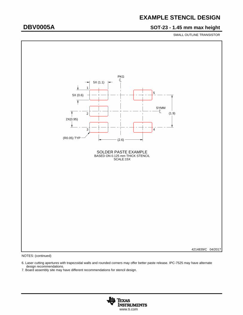
EXAMPLE STENCIL DESIGN
(2.6)
(1.9)
2X(0.95)
5X (1.1)
5X (0.6)
(R0.05) TYP
SOT-23 - 1.45 mm max heightDBV0005ASMALL OUTLINE TRANSISTOR
4214839/C 04/2017
NOTES: (continued) 6. Laser cutting apertures with trapezoidal walls and rounded corners may offer better paste release. IPC-7525 may have alternate design recommendations. 7. Board assembly site may have different recommendations for stencil design.
SOLDER PASTE EXAMPLEBASED ON 0.125 mm THICK STENCIL
SCALE:15X
SYMM
PKG
1
3 4
5
2
www.ti.com
PACKAGE OUTLINE
C
TYP0.220.08
0.25
3.02.6
2X 0.95
1.9
1.45 MAX
TYP0.150.00
5X 0.50.3
TYP0.60.3
TYP80
1.9
A
3.052.75
B1.751.45
(1.1)
SOT-23 - 1.45 mm max heightDBV0005ASMALL OUTLINE TRANSISTOR
4214839/C 04/2017
NOTES: 1. All linear dimensions are in millimeters. Any dimensions in parenthesis are for reference only. Dimensioning and tolerancing per ASME Y14.5M.2. This drawing is subject to change without notice.3. Refernce JEDEC MO-178.
0.2 C A B
1
34
5
2
INDEX AREAPIN 1
GAGE PLANE
SEATING PLANE
0.1 C
SCALE 4.000

www.ti.com
EXAMPLE BOARD LAYOUT
0.07 MAXARROUND
0.07 MINARROUND
5X (1.1)
5X (0.6)
(2.6)
(1.9)
2X (0.95)
(R0.05) TYP
4214839/C 04/2017
SOT-23 - 1.45 mm max heightDBV0005ASMALL OUTLINE TRANSISTOR
NOTES: (continued) 4. Publication IPC-7351 may have alternate designs. 5. Solder mask tolerances between and around signal pads can vary based on board fabrication site.
SYMM
LAND PATTERN EXAMPLEEXPOSED METAL SHOWN
SCALE:15X
PKG
1
3 4
5
2
SOLDER MASKOPENINGMETAL UNDER
SOLDER MASK
SOLDER MASKDEFINED
EXPOSED METAL
METALSOLDER MASKOPENING
NON SOLDER MASKDEFINED
(PREFERRED)
SOLDER MASK DETAILS
EXPOSED METAL

www.ti.com
EXAMPLE STENCIL DESIGN
(2.6)
(1.9)
2X(0.95)
5X (1.1)
5X (0.6)
(R0.05) TYP
SOT-23 - 1.45 mm max heightDBV0005ASMALL OUTLINE TRANSISTOR
4214839/C 04/2017
NOTES: (continued) 6. Laser cutting apertures with trapezoidal walls and rounded corners may offer better paste release. IPC-7525 may have alternate design recommendations. 7. Board assembly site may have different recommendations for stencil design.
SOLDER PASTE EXAMPLEBASED ON 0.125 mm THICK STENCIL
SCALE:15X
SYMM
PKG
1
3 4
5
2
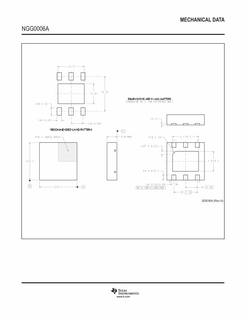
MECHANICAL DATA
NGG0006A
www.ti.com
SDE06A (Rev A)
IMPORTANT NOTICE
Texas Instruments Incorporated (TI) reserves the right to make corrections, enhancements, improvements and other changes to itssemiconductor products and services per JESD46, latest issue, and to discontinue any product or service per JESD48, latest issue. Buyersshould obtain the latest relevant information before placing orders and should verify that such information is current and complete.TI’s published terms of sale for semiconductor products (http://www.ti.com/sc/docs/stdterms.htm) apply to the sale of packaged integratedcircuit products that TI has qualified and released to market. Additional terms may apply to the use or sale of other types of TI products andservices.Reproduction of significant portions of TI information in TI data sheets is permissible only if reproduction is without alteration and isaccompanied by all associated warranties, conditions, limitations, and notices. TI is not responsible or liable for such reproduceddocumentation. Information of third parties may be subject to additional restrictions. Resale of TI products or services with statementsdifferent from or beyond the parameters stated by TI for that product or service voids all express and any implied warranties for theassociated TI product or service and is an unfair and deceptive business practice. TI is not responsible or liable for any such statements.Buyers and others who are developing systems that incorporate TI products (collectively, “Designers”) understand and agree that Designersremain responsible for using their independent analysis, evaluation and judgment in designing their applications and that Designers havefull and exclusive responsibility to assure the safety of Designers' applications and compliance of their applications (and of all TI productsused in or for Designers’ applications) with all applicable regulations, laws and other applicable requirements. Designer represents that, withrespect to their applications, Designer has all the necessary expertise to create and implement safeguards that (1) anticipate dangerousconsequences of failures, (2) monitor failures and their consequences, and (3) lessen the likelihood of failures that might cause harm andtake appropriate actions. Designer agrees that prior to using or distributing any applications that include TI products, Designer willthoroughly test such applications and the functionality of such TI products as used in such applications.TI’s provision of technical, application or other design advice, quality characterization, reliability data or other services or information,including, but not limited to, reference designs and materials relating to evaluation modules, (collectively, “TI Resources”) are intended toassist designers who are developing applications that incorporate TI products; by downloading, accessing or using TI Resources in anyway, Designer (individually or, if Designer is acting on behalf of a company, Designer’s company) agrees to use any particular TI Resourcesolely for this purpose and subject to the terms of this Notice.TI’s provision of TI Resources does not expand or otherwise alter TI’s applicable published warranties or warranty disclaimers for TIproducts, and no additional obligations or liabilities arise from TI providing such TI Resources. TI reserves the right to make corrections,enhancements, improvements and other changes to its TI Resources. TI has not conducted any testing other than that specificallydescribed in the published documentation for a particular TI Resource.Designer is authorized to use, copy and modify any individual TI Resource only in connection with the development of applications thatinclude the TI product(s) identified in such TI Resource. NO OTHER LICENSE, EXPRESS OR IMPLIED, BY ESTOPPEL OR OTHERWISETO ANY OTHER TI INTELLECTUAL PROPERTY RIGHT, AND NO LICENSE TO ANY TECHNOLOGY OR INTELLECTUAL PROPERTYRIGHT OF TI OR ANY THIRD PARTY IS GRANTED HEREIN, including but not limited to any patent right, copyright, mask work right, orother intellectual property right relating to any combination, machine, or process in which TI products or services are used. Informationregarding or referencing third-party products or services does not constitute a license to use such products or services, or a warranty orendorsement thereof. Use of TI Resources may require a license from a third party under the patents or other intellectual property of thethird party, or a license from TI under the patents or other intellectual property of TI.TI RESOURCES ARE PROVIDED “AS IS” AND WITH ALL FAULTS. TI DISCLAIMS ALL OTHER WARRANTIES ORREPRESENTATIONS, EXPRESS OR IMPLIED, REGARDING RESOURCES OR USE THEREOF, INCLUDING BUT NOT LIMITED TOACCURACY OR COMPLETENESS, TITLE, ANY EPIDEMIC FAILURE WARRANTY AND ANY IMPLIED WARRANTIES OFMERCHANTABILITY, FITNESS FOR A PARTICULAR PURPOSE, AND NON-INFRINGEMENT OF ANY THIRD PARTY INTELLECTUALPROPERTY RIGHTS. TI SHALL NOT BE LIABLE FOR AND SHALL NOT DEFEND OR INDEMNIFY DESIGNER AGAINST ANY CLAIM,INCLUDING BUT NOT LIMITED TO ANY INFRINGEMENT CLAIM THAT RELATES TO OR IS BASED ON ANY COMBINATION OFPRODUCTS EVEN IF DESCRIBED IN TI RESOURCES OR OTHERWISE. IN NO EVENT SHALL TI BE LIABLE FOR ANY ACTUAL,DIRECT, SPECIAL, COLLATERAL, INDIRECT, PUNITIVE, INCIDENTAL, CONSEQUENTIAL OR EXEMPLARY DAMAGES INCONNECTION WITH OR ARISING OUT OF TI RESOURCES OR USE THEREOF, AND REGARDLESS OF WHETHER TI HAS BEENADVISED OF THE POSSIBILITY OF SUCH DAMAGES.Unless TI has explicitly designated an individual product as meeting the requirements of a particular industry standard (e.g., ISO/TS 16949and ISO 26262), TI is not responsible for any failure to meet such industry standard requirements.Where TI specifically promotes products as facilitating functional safety or as compliant with industry functional safety standards, suchproducts are intended to help enable customers to design and create their own applications that meet applicable functional safety standardsand requirements. Using products in an application does not by itself establish any safety features in the application. Designers mustensure compliance with safety-related requirements and standards applicable to their applications. Designer may not use any TI products inlife-critical medical equipment unless authorized officers of the parties have executed a special contract specifically governing such use.Life-critical medical equipment is medical equipment where failure of such equipment would cause serious bodily injury or death (e.g., lifesupport, pacemakers, defibrillators, heart pumps, neurostimulators, and implantables). Such equipment includes, without limitation, allmedical devices identified by the U.S. Food and Drug Administration as Class III devices and equivalent classifications outside the U.S.TI may expressly designate certain products as completing a particular qualification (e.g., Q100, Military Grade, or Enhanced Product).Designers agree that it has the necessary expertise to select the product with the appropriate qualification designation for their applicationsand that proper product selection is at Designers’ own risk. Designers are solely responsible for compliance with all legal and regulatoryrequirements in connection with such selection.Designer will fully indemnify TI and its representatives against any damages, costs, losses, and/or liabilities arising out of Designer’s non-compliance with the terms and provisions of this Notice.
Mailing Address: Texas Instruments, Post Office Box 655303, Dallas, Texas 75265Copyright © 2018, Texas Instruments Incorporated