single channel smart load switchsingle channel smart load switch description and applications the...
TRANSCRIPT
DML1009LDS Document number: DS39081 Rev. 2 - 2
1 of 12 www.diodes.com
January 2017 © Diodes Incorporated
DML1009LDS
NE
W P
RO
DU
CT
AD
VA
NC
E IN
FO
RM
AT
IO
N
AD
VA
NC
ED
IN
FO
RM
AT
IO
N
SINGLE CHANNEL SMART LOAD SWITCH
Description and Applications
The DML1009LDS is a single channel load switch with very low on-
resistance in a small package. It contains an N-Channel MOSFET for
up to VBIAS-1.5V input voltage operation and 6A current channel with
3.2V to 5.5V bias supply. The load switch is controlled by a low
voltage control signal through the ON Pin.
Portable Computers
Ultrabooks
Tablet PCs
Set Top Boxes
LCD TVs
Telecom/Networking/Datacom Equipment
SSDs
Consumer Electronics
Features and Benefits
Low RDS(ON) – Ensures On-State Losses are Minimized
0.8V to VBIAS-1.5V Input Voltage Range
10A Continuous Current
Low RDS(ON) Internal NFETs
5mΩ at VBIAS = 5V, VIN = 1.05V
35µA Low Quiescent Current
10µs Turn On Rise Time
3.2V to 5.5V Bias Voltage
Integrated Quick Output Discharge Resistor
Moisture Sensitivity: Level 1 per J-STD-020
Totally Lead-Free & Fully RoHS Compliant (Notes 1 & 2)
Halogen and Antimony Free. “Green” Device (Note 3)
Ordering Information (Note 4)
Part Number Case Packaging
DML1009LDS-7 V-DFN3030-8 (Type R) 3,000/Tape & Reel
DML1009LDS-13 V-DFN3030-8 (Type R) 3,000/Tape & Reel
Notes: 1. No purposely added lead. Fully EU Directive 2002/95/EC (RoHS) & 2011/65/EU (RoHS 2) compliant. 2. See http://www.diodes.com/quality/lead_free.html for more information about Diodes Incorporated’s definitions of Halogen- and Antimony-free, "Green" and Lead-free. 3. Halogen- and Antimony-free "Green” products are defined as those which contain <900ppm bromine, <900ppm chlorine (<1500ppm total Br + Cl) and <1000ppm antimony compounds. 4. For packaging details, go to our website at http://www.diodes.com/products/packages.html.
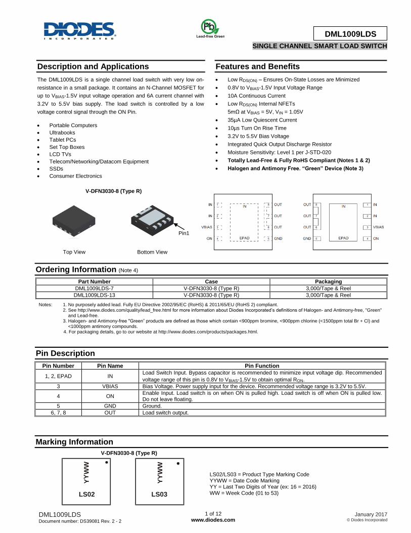
Pin Description
Pin Number Pin Name Pin Function
1, 2, EPAD IN Load Switch Input. Bypass capacitor is recommended to minimize input voltage dip. Recommended
voltage range of this pin is 0.8V to VBIAS-1.5V to obtain optimal RON.
3 VBIAS Bias Voltage. Power supply input for the device. Recommended voltage range is 3.2V to 5.5V.
4 ON Enable Input. Load switch is on when ON is pulled high. Load switch is off when ON is pulled low. Do not leave floating.
5 GND Ground.
6, 7, 8 OUT Load switch output.
Marking Information
Bottom View Top View
V-DFN3030-8 (Type R)
Pin1
LS02/LS03 = Product Type Marking Code YYWW = Date Code Marking YY = Last Two Digits of Year (ex: 16 = 2016) WW = Week Code (01 to 53)
Y
LS02
Y
WW
V-DFN3030-8 (Type R)
YY
WW
LS03
DML1009LDS Document number: DS39081 Rev. 2 - 2
2 of 12 www.diodes.com
January 2017 © Diodes Incorporated
DML1009LDS
NE
W P
RO
DU
CT
AD
VA
NC
E IN
FO
RM
AT
IO
N
AD
VA
NC
ED
IN
FO
RM
AT
IO
N
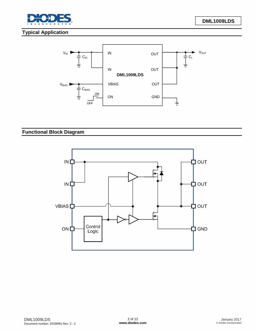
Typical Application
IN
IN
VBIAS
ON
OUT
GND
OUT
OUTVBIAS
VINVOUT
CLCIN
CBIAS
OFF
ON
Functional Block Diagram
DML1009LDS
DML1009LDS Document number: DS39081 Rev. 2 - 2
3 of 12 www.diodes.com
January 2017 © Diodes Incorporated
DML1009LDS
NE
W P
RO
DU
CT
AD
VA
NC
E IN
FO
RM
AT
IO
N
AD
VA
NC
ED
IN
FO
RM
AT
IO
N
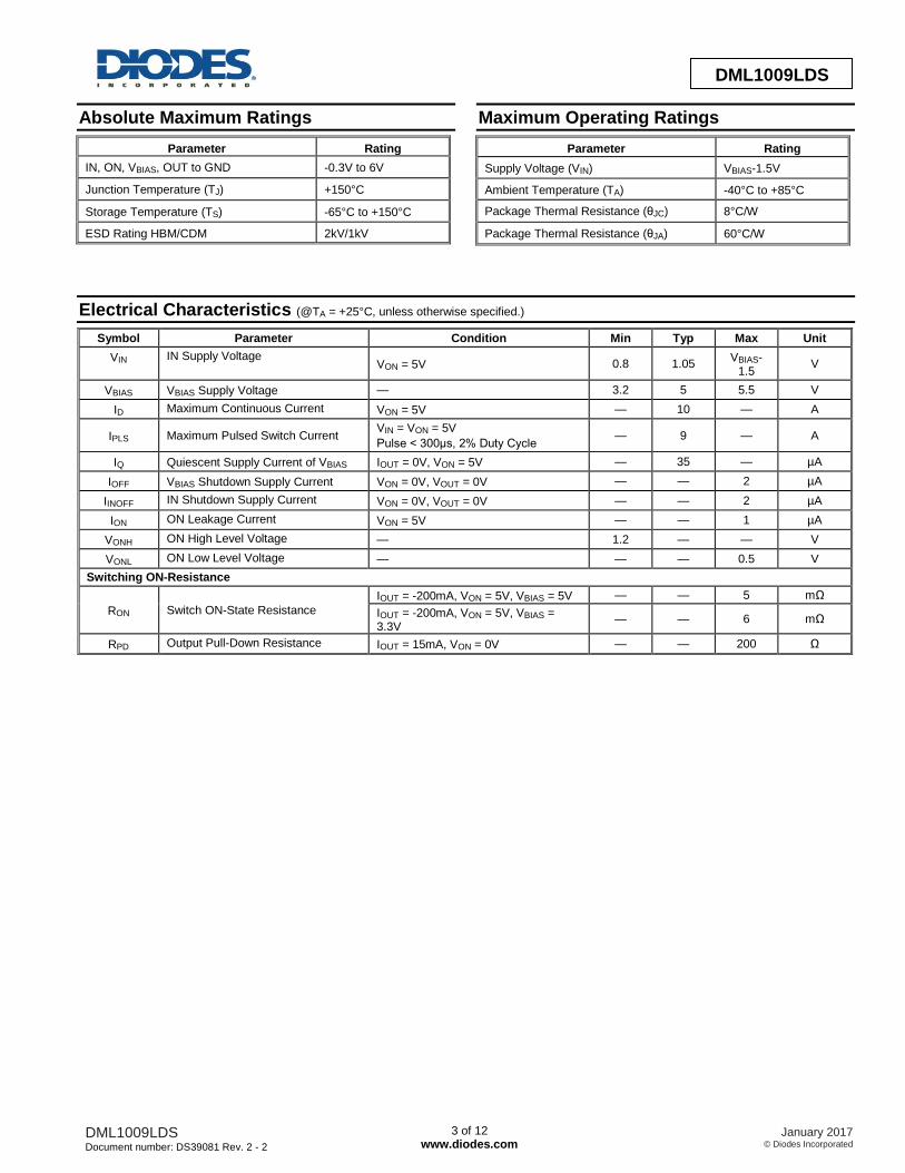
Absolute Maximum Ratings
Parameter Rating
IN, ON, VBIAS, OUT to GND -0.3V to 6V
Junction Temperature (TJ) +150°C
Storage Temperature (TS) -65°C to +150°C
ESD Rating HBM/CDM 2kV/1kV
Maximum Operating Ratings
Parameter Rating
Supply Voltage (VIN) VBIAS-1.5V
Ambient Temperature (TA) -40°C to +85°C
Package Thermal Resistance (θJC) 8°C/W
Package Thermal Resistance (θJA) 60°C/W
Electrical Characteristics (@TA = +25°C, unless otherwise specified.)
Symbol Parameter Condition Min Typ Max Unit
VIN IN Supply Voltage VON = 5V 0.8 1.05
VBIAS-1.5
V
VBIAS VBIAS Supply Voltage — 3.2 5 5.5 V
ID Maximum Continuous Current VON = 5V — 10 — A
IPLS Maximum Pulsed Switch Current VIN = VON = 5V
Pulse < 300μs, 2% Duty Cycle — 9 — A
IQ Quiescent Supply Current of VBIAS IOUT = 0V, VON = 5V — 35 — µA
IOFF VBIAS Shutdown Supply Current VON = 0V, VOUT = 0V — — 2 µA
IINOFF IN Shutdown Supply Current VON = 0V, VOUT = 0V — — 2 µA
ION ON Leakage Current VON = 5V — — 1 µA
VONH ON High Level Voltage — 1.2 — — V
VONL ON Low Level Voltage — — — 0.5 V
Switching ON-Resistance
RON Switch ON-State Resistance
IOUT = -200mA, VON = 5V, VBIAS = 5V — — 5 mΩ
IOUT = -200mA, VON = 5V, VBIAS = 3.3V
— — 6 mΩ
RPD Output Pull-Down Resistance IOUT = 15mA, VON = 0V — — 200 Ω
DML1009LDS Document number: DS39081 Rev. 2 - 2
4 of 12 www.diodes.com
January 2017 © Diodes Incorporated
DML1009LDS
NE
W P
RO
DU
CT
AD
VA
NC
E IN
FO
RM
AT
IO
N
AD
VA
NC
ED
IN
FO
RM
AT
IO
N
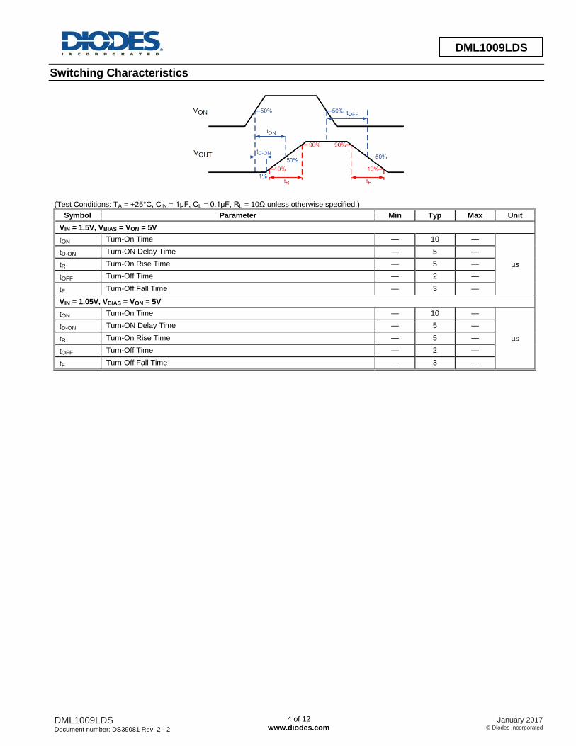
Switching Characteristics
(Test Conditions: TA = +25°C, CIN = 1μF, CL = 0.1μF, RL = 10Ω unless otherwise specified.)
Symbol Parameter Min Typ Max Unit
VIN = 1.5V, VBIAS = VON = 5V
tON Turn-On Time — 10 —
µs
tD-ON Turn-ON Delay Time — 5 —
tR Turn-On Rise Time — 5 —
tOFF Turn-Off Time — 2 —
tF Turn-Off Fall Time — 3 —
VIN = 1.05V, VBIAS = VON = 5V
tON Turn-On Time — 10 —
µs
tD-ON Turn-ON Delay Time — 5 —
tR Turn-On Rise Time — 5 —
tOFF Turn-Off Time — 2 —
tF Turn-Off Fall Time — 3 —
DML1009LDS Document number: DS39081 Rev. 2 - 2
5 of 12 www.diodes.com
January 2017 © Diodes Incorporated
DML1009LDS
NE
W P
RO
DU
CT
AD
VA
NC
E IN
FO
RM
AT
IO
N
AD
VA
NC
ED
IN
FO
RM
AT
IO
N
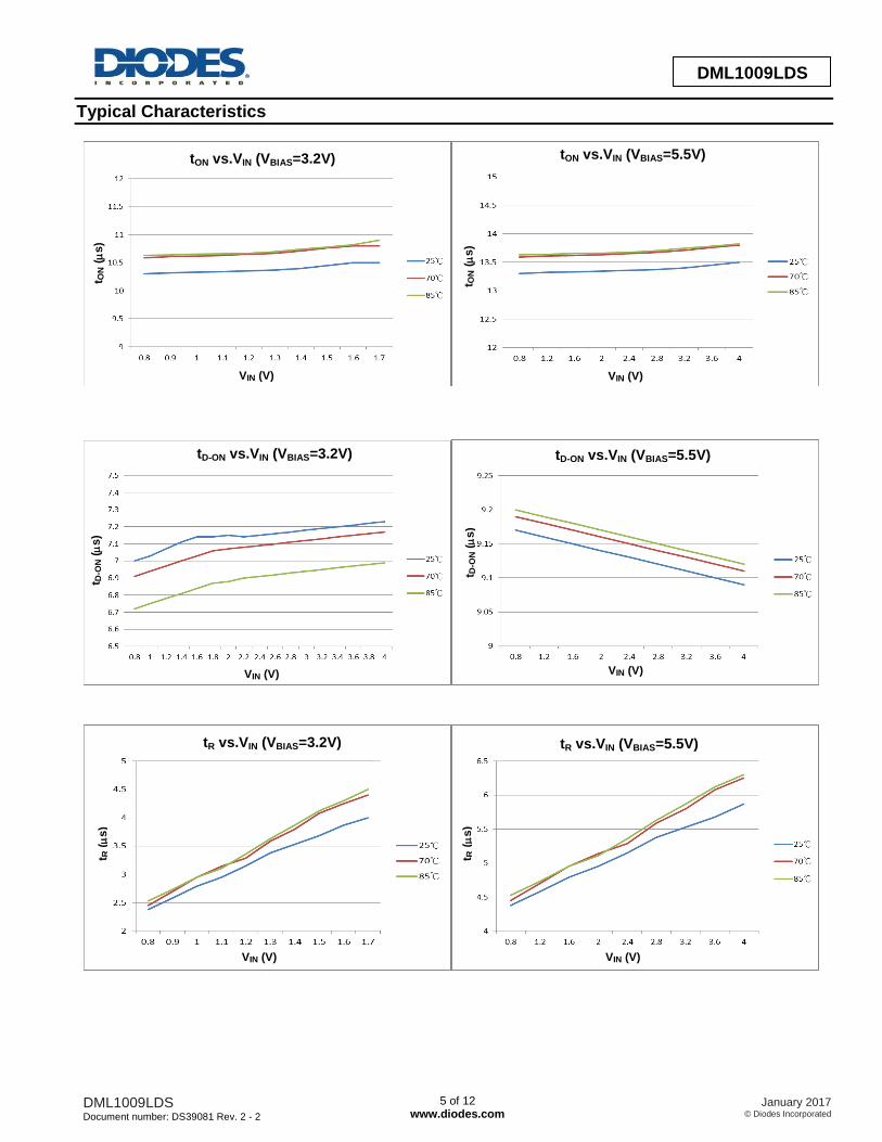
Typical Characteristics
tON vs.VIN (VBIAS=3.2V)
tD-ON vs.VIN (VBIAS=3.2V) tD-ON vs.VIN (VBIAS=5.5V)
tR vs.VIN (VBIAS=3.2V) tR vs.VIN (VBIAS=5.5V)
VIN (V)
VIN (V)
VIN (V)
VIN (V)
tON vs.VIN (VBIAS=5.5V)
VIN (V)
t ON (
s)
t D-O
N (
s)
t D-O
N (
s)
t R (
s)
t R (
s)
t ON (
s)
VIN (V)
DML1009LDS Document number: DS39081 Rev. 2 - 2
6 of 12 www.diodes.com
January 2017 © Diodes Incorporated
DML1009LDS
NE
W P
RO
DU
CT
AD
VA
NC
E IN
FO
RM
AT
IO
N
AD
VA
NC
ED
IN
FO
RM
AT
IO
N
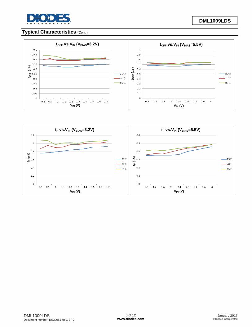
Typical Characteristics (Cont.)
tF vs.VIN (VBIAS=3.2V) tF vs.VIN (VBIAS=5.5V)
tOFF vs.VIN (VBIAS=3.2V) tOFF vs.VIN (VBIAS=5.5V)
t OF
F (
s)
t OF
F (
s)
VIN (V)
VIN (V)
t F (
s)
t F (
s)
VIN (V) VIN (V)
DML1009LDS Document number: DS39081 Rev. 2 - 2
7 of 12 www.diodes.com
January 2017 © Diodes Incorporated
DML1009LDS
NE
W P
RO
DU
CT
AD
VA
NC
E IN
FO
RM
AT
IO
N
AD
VA
NC
ED
IN
FO
RM
AT
IO
N
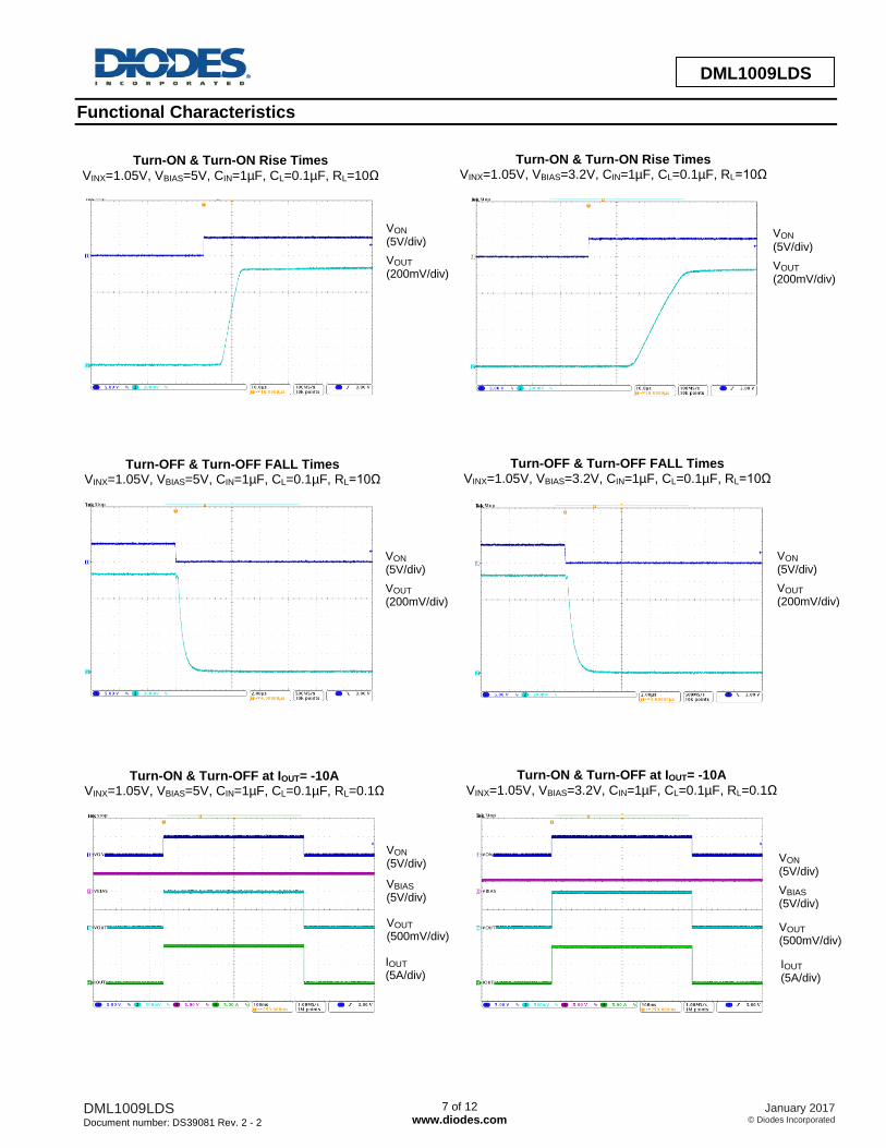
Functional Characteristics
Turn-ON & Turn-ON Rise Times
VINX=1.05V, VBIAS=5V, CIN=1µF, CL=0.1µF, RL=10Ω
Turn-ON & Turn-ON Rise Times VINX=1.05V, VBIAS=3.2V, CIN=1µF, CL=0.1µF, RL=10Ω
VOUT
(200mV/div)
VON
(5V/div)
VOUT
(200mV/div)
VON
(5V/div)
Turn-OFF & Turn-OFF FALL Times VINX=1.05V, VBIAS=5V, CIN=1µF, CL=0.1µF, RL=10Ω
Turn-OFF & Turn-OFF FALL Times VINX=1.05V, VBIAS=3.2V, CIN=1µF, CL=0.1µF, RL=10Ω
VOUT
(200mV/div)
VON
(5V/div)
VOUT
(200mV/div)
VON
(5V/div)
Turn-ON & Turn-OFF at IOUT= -10A VINX=1.05V, VBIAS=5V, CIN=1µF, CL=0.1µF, RL=0.1Ω
Turn-ON & Turn-OFF at IOUT= -10A
VINX=1.05V, VBIAS=3.2V, CIN=1µF, CL=0.1µF, RL=0.1Ω
VBIAS
(5V/div)
VON
(5V/div)
IOUT
(5A/div)
VOUT
(500mV/div)
VBIAS
(5V/div)
VON
(5V/div)
IOUT
(5A/div)
VOUT
(500mV/div)
DML1009LDS Document number: DS39081 Rev. 2 - 2
8 of 12 www.diodes.com
January 2017 © Diodes Incorporated
DML1009LDS
NE
W P
RO
DU
CT
AD
VA
NC
E IN
FO
RM
AT
IO
N
AD
VA
NC
ED
IN
FO
RM
AT
IO
N
Detailed Description
ON/OFF Control
The DML1009LDS is enabled when the ON Pin is on active high with voltage of 1.2V or above. The device is disabled when the ON Pin voltage is
0.5V or lower. The EN input is compatible with both TTL and CMOS logic.
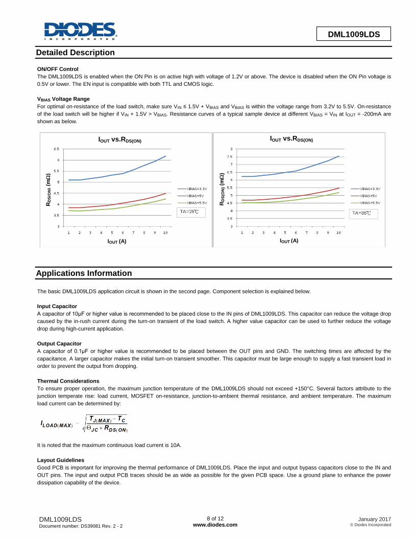
VBIAS Voltage Range
For optimal on-resistance of the load switch, make sure VIN ≤ 1.5V + VBIAS and VBIAS is within the voltage range from 3.2V to 5.5V. On-resistance
of the load switch will be higher if VIN + 1.5V > VBIAS. Resistance curves of a typical sample device at different VBIAS = VIN at IOUT = -200mA are
shown as below.
Applications Information
The basic DML1009LDS application circuit is shown in the second page. Component selection is explained below.
Input Capacitor
A capacitor of 10μF or higher value is recommended to be placed close to the IN pins of DML1009LDS. This capacitor can reduce the voltage drop
caused by the in-rush current during the turn-on transient of the load switch. A higher value capacitor can be used to further reduce the voltage
drop during high-current application.
Output Capacitor
A capacitor of 0.1μF or higher value is recommended to be placed between the OUT pins and GND. The switching times are affected by the
capacitance. A larger capacitor makes the initial turn-on transient smoother. This capacitor must be large enough to supply a fast transient load in
order to prevent the output from dropping.
Thermal Considerations
To ensure proper operation, the maximum junction temperature of the DML1009LDS should not exceed +150°C. Several factors attribute to the
junction temperate rise: load current, MOSFET on-resistance, junction-to-ambient thermal resistance, and ambient temperature. The maximum
load current can be determined by:
It is noted that the maximum continuous load current is 10A.
Layout Guidelines
Good PCB is important for improving the thermal performance of DML1009LDS. Place the input and output bypass capacitors close to the IN and
OUT pins. The input and output PCB traces should be as wide as possible for the given PCB space. Use a ground plane to enhance the power
dissipation capability of the device.
IOUT vs.RDS(ON) IOUT vs.RDS(ON)
RD
S(O
N)
(m
)
RD
S(O
N) (m
)
IOUT (A) IOUT (A)
DML1009LDS Document number: DS39081 Rev. 2 - 2
9 of 12 www.diodes.com
January 2017 © Diodes Incorporated
DML1009LDS
NE
W P
RO
DU
CT
AD
VA
NC
E IN
FO
RM
AT
IO
N
AD
VA
NC
ED
IN
FO
RM
AT
IO
N
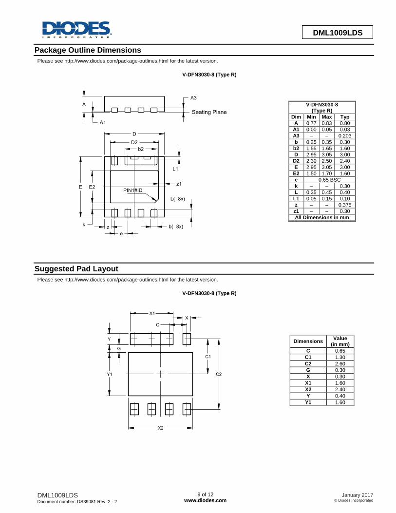
Package Outline Dimensions
Please see http://www.diodes.com/package-outlines.html for the latest version.
V-DFN3030-8 (Type R)
Seating Plane
D
D2
E E2
b(8x)
L(8x)
e
b2
L1
A
A1
A3
zk
z1
PIN1#ID
V-DFN3030-8 (Type R)
Dim Min Max Typ
A 0.77 0.83 0.80
A1 0.00 0.05 0.03
A3 – – 0.203
b 0.25 0.35 0.30
b2 1.55 1.65 1.60
D 2.95 3.05 3.00
D2 2.30 2.50 2.40
E 2.95 3.05 3.00
E2 1.50 1.70 1.60
e 0.65 BSC
k – – 0.30
L 0.35 0.45 0.40
L1 0.05 0.15 0.10
z – – 0.375
z1 – – 0.30
All Dimensions in mm
Suggested Pad Layout
Please see http://www.diodes.com/package-outlines.html for the latest version.
V-DFN3030-8 (Type R)
Y1
X2
C2
C1
X
C
X1
Y
G
Dimensions Value
(in mm)
C 0.65
C1 1.30
C2 2.60
G 0.30
X 0.30
X1 1.60
X2 2.40
Y 0.40
Y1 1.60
DML1009LDS Document number: DS39081 Rev. 2 - 2
10 of 12 www.diodes.com
January 2017 © Diodes Incorporated
DML1009LDS
NE
W P
RO
DU
CT
AD
VA
NC
E IN
FO
RM
AT
IO
N
AD
VA
NC
ED
IN
FO
RM
AT
IO
N
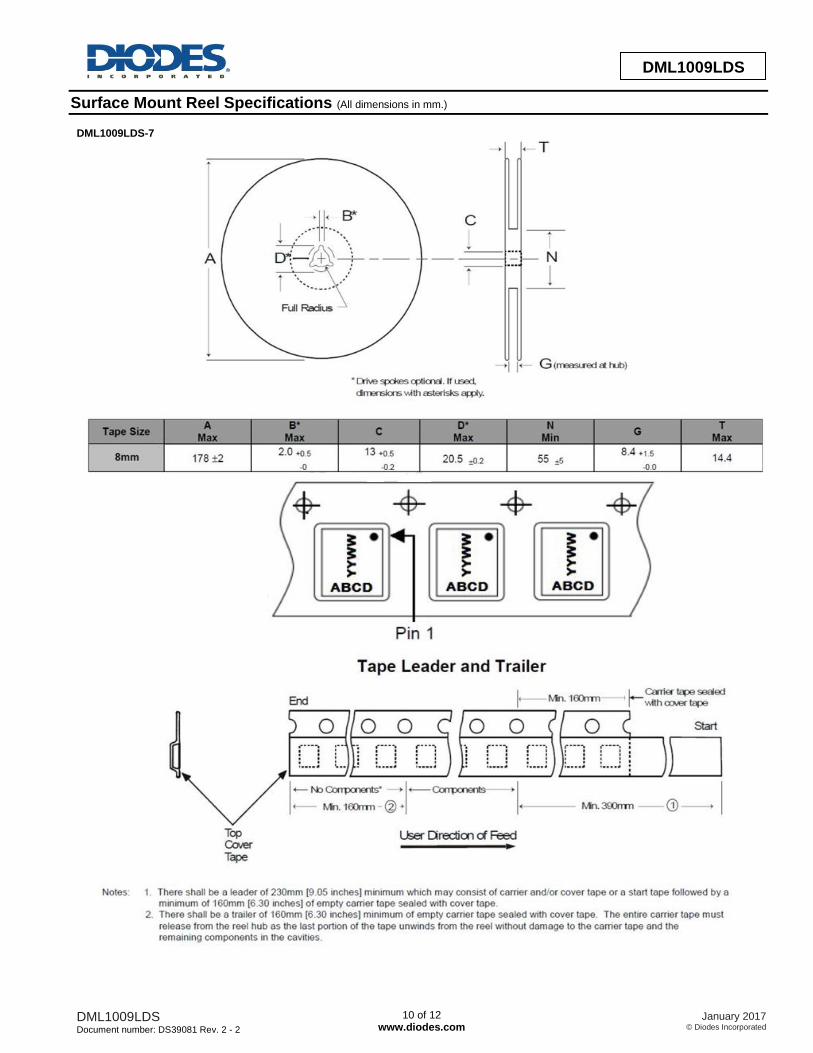
Surface Mount Reel Specifications (All dimensions in mm.) DML1009LDS-7
DML1009LDS Document number: DS39081 Rev. 2 - 2
11 of 12 www.diodes.com
January 2017 © Diodes Incorporated
DML1009LDS
NE
W P
RO
DU
CT
AD
VA
NC
E IN
FO
RM
AT
IO
N
AD
VA
NC
ED
IN
FO
RM
AT
IO
N
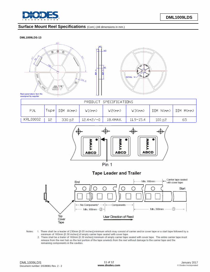
Surface Mount Reel Specifications (Cont.) (All dimensions in mm.) DML1009LDS-13
DML1009LDS Document number: DS39081 Rev. 2 - 2
12 of 12 www.diodes.com
January 2017 © Diodes Incorporated
DML1009LDS
NE
W P
RO
DU
CT
AD
VA
NC
E IN
FO
RM
AT
IO
N
AD
VA
NC
ED
IN
FO
RM
AT
IO
N
IMPORTANT NOTICE DIODES INCORPORATED MAKES NO WARRANTY OF ANY KIND, EXPRESS OR IMPLIED, WITH REGARDS TO THIS DOCUMENT, INCLUDING, BUT NOT LIMITED TO, THE IMPLIED WARRANTIES OF MERCHANTABILITY AND FITNESS FOR A PARTICULAR PURPOSE (AND THEIR EQUIVALENTS UNDER THE LAWS OF ANY JURISDICTION). Diodes Incorporated and its subsidiaries reserve the right to make modifications, enhancements, improvements, corrections or other changes without further notice to this document and any product described herein. Diodes Incorporated does not assume any liability arising out of the application or use of this document or any product described herein; neither does Diodes Incorporated convey any license under its patent or trademark rights, nor the rights of others. Any Customer or user of this document or products described herein in such applications shall assume all risks of such use and will agree to hold Diodes Incorporated and all the companies whose products are represented on Diodes Incorporated website, harmless against all damages. Diodes Incorporated does not warrant or accept any liability whatsoever in respect of any products purchased through unauthorized sales channel. Should Customers purchase or use Diodes Incorporated products for any unintended or unauthorized application, Customers shall indemnify and hold Diodes Incorporated and its representatives harmless against all claims, damages, expenses, and attorney fees arising out of, directly or indirectly, any claim of personal injury or death associated with such unintended or unauthorized application. Products described herein may be covered by one or more United States, international or foreign patents pending. Product names and markings noted herein may also be covered by one or more United States, international or foreign trademarks. This document is written in English but may be translated into multiple languages for reference. Only the English version of this document is the final and determinative format released by Diodes Incorporated.
LIFE SUPPORT Diodes Incorporated products are specifically not authorized for use as critical components in life support devices or systems without the express written approval of the Chief Executive Officer of Diodes Incorporated. As used herein: A. Life support devices or systems are devices or systems which: 1. are intended to implant into the body, or
2. support or sustain life and whose failure to perform when properly used in accordance with instructions for use provided in the labeling can be reasonably expected to result in significant injury to the user.
B. A critical component is any component in a life support device or system whose failure to perform can be reasonably expected to cause the failure of the life support device or to affect its safety or effectiveness. Customers represent that they have all necessary expertise in the safety and regulatory ramifications of their life support devices or systems, and acknowledge and agree that they are solely responsible for all legal, regulatory and safety-related requirements concerning their products and any use of Diodes Incorporated products in such safety-critical, life support devices or systems, notwithstanding any devices- or systems-related information or support that may be provided by Diodes Incorporated. Further, Customers must fully indemnify Diodes Incorporated and its representatives against any damages arising out of the use of Diodes Incorporated products in such safety-critical, life support devices or systems. Copyright © 2017, Diodes Incorporated www.diodes.com