simple ssb transceiver - island labssimple ssb transceiver sl600 version this transceiver, shown in...
TRANSCRIPT
58
Simple SSB transceiver SL600 VERSION
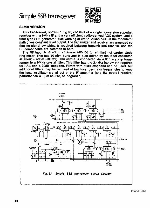
This transceiver, shown in Fig.63, consists of a single conversion superhet receiver with a 9MHz IF and a very efficient audio-derived AGC system, and a filter type SSB generator, also working at 9MHz. Audio AGC in the modulator path gives constant level output. The transmitter and receiver are arranged so that no signal switching is required between transmit and receive, and the RF components are common to both.
The RF input is direct to an Anzac MO-108 (or similar) hot carrier diode ring mixer. This has 50 ohm ports and is also driven by the local oscillator, at about T 7dBm (500mV). The output is connected via a 3: 1 step-up transformer to a 9MHz crystal filter. This filter has the 2.4kHz bandwidth required for SSB and a 90dB stopband. Filters with 60dB stopband can be used, but additional filters may be required at low local oscillator frequencies to keep the local oscillator signal out of the IF amplifier (and the overall receiver performance will, of course, be degraded).
C31.~f-+-1
TRANSMIT OAIN
CONTROL
1'-----,...-----< ~~ ~-+------< INPUT
~=+--,,""""----+----+----;-~'s' METER
VOLUME CONTI!OL
Flg.63 Simple SSB transceiver circuit diagram
Island Labs
The filter used, an SEI QC1246AX or a KVG XF9-B, has a terminating impedance of 500 ohms, but only within the passband of the filter. At frequencies outside the passband it may be very different, which means that the impedance that the filter presents to the diode ring mixer via the transformer will vary from 50 ohms. Such a mismatch will degrade the cross-modulation and carrier leak performance of the diode ring. However, it was decided on balance, that it was better to tolerate such degradation - which is not excessive -than to complicate the design by incorporating a broadband impedance match (which would probably not be bidirectional and hence would have to be switched between transmit and receive).
The present design allows the same arrangement to operate in opposite directions during receive and transmit without any switching. On the other side of the crystal filter the transmit and receive signal paths diverge but are sti II not switched.
The Receiver The incoming RF signal is mixed with the local oscillator in the mixer
described above and then passes through an SSB bandwidth 9MHz crystal filter. It is then amplified by three cascaded SL612C IF amplifiers, IC2, 3 and 4. These amplifiers are untuned and since the strip has a maximum gain of 102dB careful attention must be paid both to noise and to stability. The SL612C has a 3dB noise figure which means that the broadband noise at the output of the three-stage strip is about 10mV RMS. This is not sufficient to affect a product detector, which is only concerned with the component within a few kHz of the BFO frequency, but would cause trouble if a diode detector were to be used.
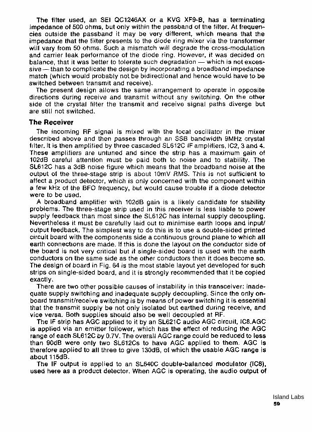
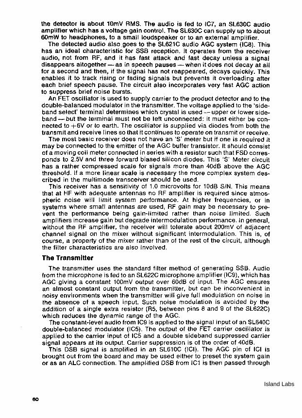
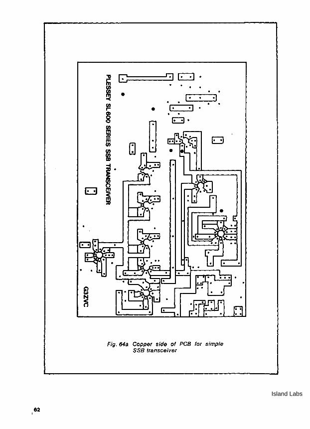
A broadband amplifier with 102dB gain is a likely candidate for stability problems. The three-stage strip used in this receiver is less liable to power supply feedback than most since the SL612C has internal supply decoupling. Nevertheless it must be carefully laid out to minimise earth loops and inputl output feedback. The simplest way to do this is to use a double-sided printed circuit board with the components side a continuous ground plane to which all earth connections are made. If this is done the layout on the conductor side of the board is not very critical but if single-sided board is used with the earth conductors on the same side as the other conductors then it does become so. The design of board in Fig. 64 is the most stable layout yet developed for such strips on single-sided board, and it is strongly recommended that it be copied exactly.
There are two other possible causes of instability in this transceiver: inadequate supply switching and inadequate supply decoupling. Since the only onboard transmit/receive switching is by means of power switching it is essential that the transmit supply be not only isolated but earthed during receive, and vice versa. Both supplies should also be well decoupled at RF.
The IF strip has AGC applied to it by an SL621C audio AGC circuit, ICB.AGC is applied via an emitter follower, which has the effect of reducing the AGC range of each SL612C by 0.7V. The overall AGC range could be reduced to less than 90dB were only two SL612Cs to have AGC applied to them. AGC is therefore applied to al\ three to give 130dB, of which the usable AGC range is about 115dB.
The IF output is applied to an SL640C double-balanced modulator (IC6), used here as a product detector. When AGC is operating, the audio output of
59 Island Labs
60
the detector is about 10mV RMS. The audio is fed to IC7, an SL630C audio amplifier which has a voltage gain control. The SL630C can supply up to about 60mW to headphones, to a small loudspeaker or to an external amplifier.
The detected audio also goes to the SL621C audio AGC system (IC8). This has an ideal characteristic for SSB reception. It operates from the receiver audio, not from RF, and it has fast attack and fast decay unless a Signal disappears altogether - as in speech pauses - when it does not decay at all for a second and then, if the signal has not reappeared, decays quickly. This enables it to track rising or fading signals but prevents it overloading after each brief speech pause. The circuit also incorporates very fast AGC action to suppress brief noise bursts.
An FET oscillator is used to supply carrier to the product detector and to the double-balanced modulator in the transmitter. The voltage applied to the 'sideband select' terminal determines which crystal is used - upper or lower sideband - but the terminal must not be left unconnected: it must either be connected to +6V or to earth. The oscillator is supplied via diodes from both the transmit and receive lines so that it continues to operate on transmit or receive.
The most basic receiver does not have an'S' meter but if one is required it may be connected to the emitter of the AGC buffer transistor. It should consist of a moving coil meter connected in series with a resistor such that FSD corresponds to 2.5Vand three forward biased silicon diodes. This 'S' Meter circuit has a rather compressed scale for signals more than 40dB above the AGC threshold. If a more linear scale is necessary the more complex system described in the multi mode transceiver should be used.
This receiver has a sensitivity of 1.0 microvolts for 10dB SIN. This means that at HF with adequate antennas no RF amplifier is required since atmospheric noise will limit system performance. At higher frequencies, or in systems where small antennas are used, RF gain may be necessary to prevent the performance being gain-limited rather than noise limited. Such amplifiers increase gain but degrade intermodulation performance. In general, without the RF amplifier, the receiver will tolerate about 200mV of adjacent channel signal on the mixer without significant intermodulation. This is, of course, a property of the mixer rather than of the rest of the circuit, although the filter characteristics are also involved.
The Transmitter
The transmitter uses the standard filter method of generating SSB. Audio from the microphone is fed to an SL622C microphone amplifier (IC9), which has AGC giving a constant 100mV output over 60dB of input. The AGC ensures an almost constant output from the transmitter, but can be inconvenient in noisy environments when the transmitter will give full modulation on noise in the absence of a speech input. Such noise modulation is avoided by the addition of a single extra resistor (R5, between pins 8 and 9 of the SL622C) which reduces the dynamic range of the AGC.
The constant-level audio from IC9 is applied to the signal input of an SL640C double-balanced modulator (IC5). The output of the FET carrier oscillator is applied to the carrier input of IC5 and a double sideband suppressed carrier signal appears at its output. Carrier suppression is of the order of 40dB.
This DSB signal is amplified in an SL610C (ICI). The AGC pin of ICI is brought out from the board and may be used either to preset the system gain or as an ALC connection. The amplified DSB from IC1 is then passed through
Island Labs
the crystal filter, which removes one sideband, leaving SSB. The SSB is mixed to the final transmitter frequency in the diode ring mixer and then goes to a linear amplifier which raises it to the transmitter output level. The output from the diode ring is, of course. lower than the input to the filter and is about 100mV or less into 50 ohms.
The output of IC5 and the input of the first SL612C (lC2) are connected to the same point on the filter via resistors. R6 is merely a buffer resistor but R2 and R1 set the impedance which the filter sees in operation. This varies from 480 ohms on transmit to about 530 ohms on receive, but this small variation does not affect filter performance. The loading effects of a turned-off SL612C during transmission and a turned-off SL610C during reception are similarly insignificant.
The transmitter output (atthe diode ring) consists of an SSB signal with carrier below - 55dB and opposite sideband below - 60dB, provided that the carrier oscillator is at the correct frequency. The degree of off-channel spurious signals depends on the crystal filter used: 90dB stopband type gives excellent performance but a cheaper one can sometimes cause trouble.
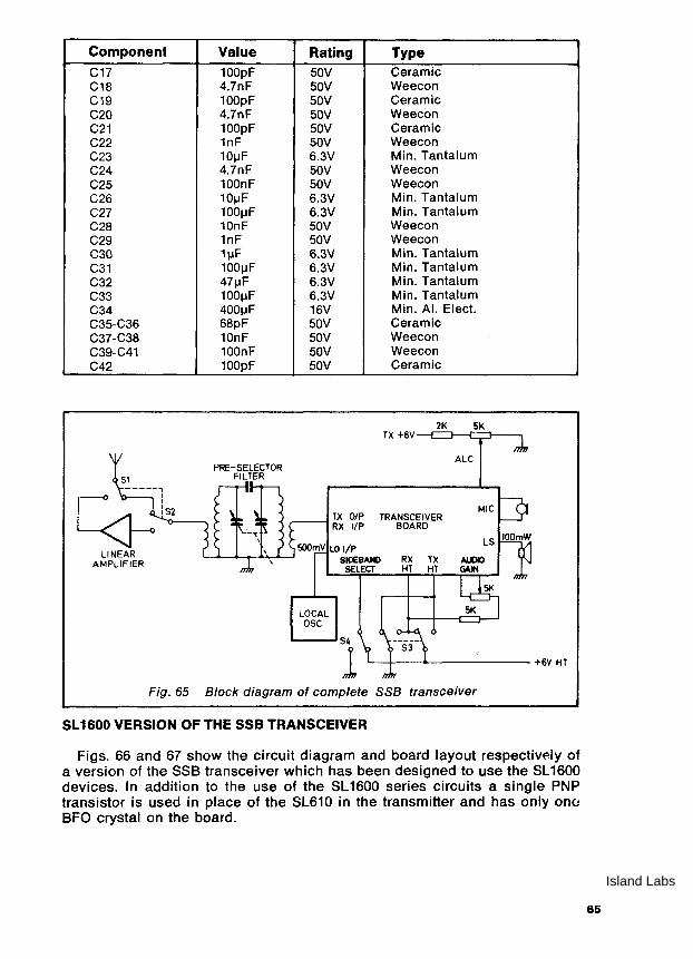
The Transceiver
The transceiver board needs few extra sub-systems to make a complete transceiver. They are: a power supply, microphone, volume control and loudspeaker and also a filter, local oscillator and linear amplifier. These are connected as shown in Fig. 65.
Much of the performance of the final system will depend upon the standard of design of the local oscillator, pre-selector, RF amplifier (if used) and linear amplifier, but the performance of the transceiver board itself is excellent. The Anzac MO-108 mixer used is capable of the required performance between 10kHz and 500MHz. If other diode rings were used the transceiver might be used over an even wider range. Its power consumption is about 400mW on either transmit or receive.
The most attractive feature of this transceiver, despite its high performance, is its simplicity. It uses only 80 components and contains no tuned circuits or other components requiring adjustment. It was designed for two purposes: (a) to demonstrate the usefulness and versatility of the SL600 Series in SSB applications and (b) as a ready-engineered SSB transceiver suitable for those inexperienced in SSB design. It is capable of giving good performance but can be constructed and commissioned by relatively inexperienced personnel.
Physical Construction
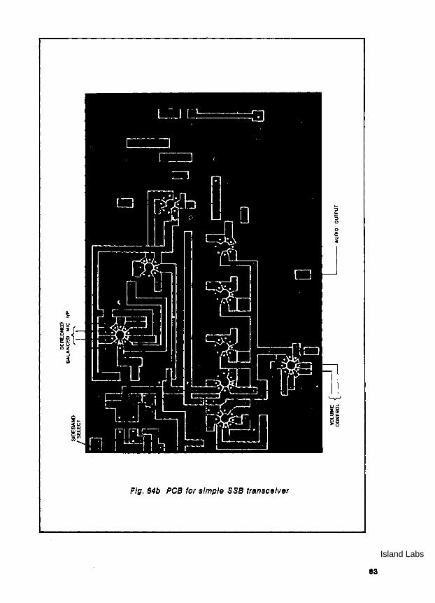
The board and component layouts are shown in Fig. 64. The board is singlesided and there are two jumper links on it carrying power supplies. As mentioned above the layout on a single-sided board carrying such a high gain broadband IF strip is critical and it should not be changed. All passive component leads should be as short as possible and integrated circuits should not be mounted more than 6mm above the board.
The two transformers T1 and T2 are both wound on small toroids of high frequency ferrite. The exact size and material are not important but the material must be low loss up to at least 45MHz and it is essential that it has a linear B/H characteristic, otherwise it will cause intermodulation at the receiver
61
Island Labs
E3
~ G: ....,~ . m • I · ·1 fa • I· ·1 8
[J ~ E3 ·
U)
!D m E3
I )13 I
..... . . m
~ :xl
Fig.64a Copper side of PCB for simple S SB transceiver
Island Labs
ffi~{ zS w ~ffi uu IIIZ
c(
~
Fig. 64b PCB for simple SSB transceiver
83
Island Labs
84
input. T2 is a simple transformer with a six-turn primary and a single turn secondary but T1 is more complex. T1 is made from four 5cm lengths of 26 SWG (0.46mm dia.) enamelled copper wire twisted together. The length of twist is used to wind two turns on the toroid and the ends are separated. Three lengths are then connected in series in the same sense to form the filter winding and the last length is used as the diode ring winding.
There are few other constructional details that need mentioning, but if a receiver without a transmitter is required one may be built by omitting the three transmitting integrated circuits (SL610C, SL622C and the SL640C) between them), R1 to R5 inclusive and C1 to C13 and C40. To preserve the filter impedance match a 500 ohm resistor should be connected from the filter side of R6 to earth.
Component Value Rating Type
R1 100 1/8 W Hi-Stab. R2 430 1/8 W Hi-Stab. R3 100 118 W Hi-Stab. R4 680K 1/8 W Hi-Stab. R5 1K 1/8 W Hi-Stab. R6 50 1/8 W Hi-Stab. R7-R9 100 1/8 W Hi-Stab. R10 330 1/8 W Hi-Stab. R11 10 1/8 W Hi-Stab. R12 100K 118 W Hi-Stab. R13 330 1/8 W Hi-Stab. 01-06 lN4148 } Or similar TR1 2N3819 devices TR2 2N706 T1, T2 See text. Mixer Anzac
MO-108 Crystals 9.0015 MHz & Parallel (30p) resonant
8.9985 MHz IC1 SL610C IC2-IC4 SL612C IC5-IC6 SL640C IC7 SL630C IC8 SL621C IC9 SL622C C1-C4 1nF 50V Weecon (Min Ceramic) C5 10J,lF 6.3V Min. Tantalum C6 100pF 50 Ceramic C7 47J,1F 6.3V Min. Tantalum C8 10J,lF 6.3V Min. Tantalum C9 4.7nF 50V Weecon C10 2J,1F n.3V Min. Tantalum C11-C12 1nF 50V Weecon C13 100nF 50V Weecon C14-C15 100pF 50V Ceramic C16 4.7nF 50V Weecon
Table 4 Components list for the Simple SSB Transceiver (Fig. 63)
Island Labs
Component
C17 C18 C19 C20 C21 C22 C23 C24 C25 C26 C27 C28 C29 C30 C31 C32 C33 C34 C35-C36 C37-C38 C39-C41 C42
~'_iS2. LINEAR
AMPLIFIER
Value 100pF 4.7nF 100pF 4.7nF 100pF 1nF 10IJF 4.7nF 100nF 10IJF 100IJF 10nF 1nF 1IJF 100IJF 47IJF 100IJF 400IJF 68pF 10nF 100nF 100pF
PRE-SELECTOR FILTER
Rating Type 50V Ceramic 50V Weecon 50V Ceramic 50V Weecon 50V Ceramic 50V Weecon 6.3V Min. Tantalum 50V Weecon 50V Weecon 6.3V Min. Tantalum 6.3V Min. Tantalum 50V Weecon 50V Weecon 6.3V Min. Tantalum 6.3V Min. Tantalum 6.3V Min. Tantalum 6.3V Min. Tantalum 16V Min. AI. Elect. 50V Ceramic 50V Weecon 50V Weecon 50V Ceramic
2K SK TX +6V --{-}--r-"'1----.
ALC
MIC TX OIP TRANSCEIVER
LOCAL OSC
RX liP BOARD
l....--4----4-.------ +6V HT
Fig.65 Block diagram of complete SSB transceiver
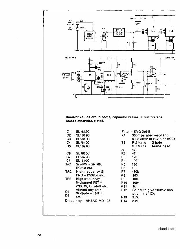
SL 1600 VERSION OF THE SSB TRANSCEIVER
Figs. 66 and 67 show the circuit diagram and board layout respectively of a version of the SSB transceiver which has been designed to use the SL 1600 devices. In addition to the use of the SL 1600 series circuits a single PNP transistor is used in place of the SL610 in the transmitter and has only on<: BFO crystal on the board.
65
Island Labs
66
RF _ SKT 1 INPUT I OUTPUT
LO INPUT
+6V TX P7 o--------.---~-..._ ___ --t_______, -0 Pll +6V SL
BALANCED{P8 ""e INPUT
1110 ... , P9~6T~_~
07
R12
Resistor values are In ohms, capacitor values In microfarads unle.s otherwise stated.
IC1 SL 1612C Filter - KVG Xf9-B IC2 SL 1612C X1 30pF parallel resonant IC3 SL 1612C 8998 5kHz in HC18 or HC25 IC4 SL 1640C T1 P 2 turns 2 hole IC5 SL 1621C S 5 turns ferrite bead
R1 470 IC6 SL1630C R2 47 IC7 SL 1622C R3 120 IC8 SL 1640C R4 120 TR1 Si NPN - 2N706, R5 120
BC108 etc. R6 10 TR2 High frequency Si R7 470k
PND - 2N3906 etc. R8 100 TR3 High frequency R9 100
N-channel FET - R10 100k 2N3819, BF244B etc. R11 1k
01 Almost any small R12 Select to give 200mV rms
02 Si diode - 1N914 at pin 4 of IC4 etc. R13 2.7k
Diode ring - ANZAC MD-108 R14 8.2k
Island Labs
------~---____1r__---_._--___._--_--~ PI HV RX
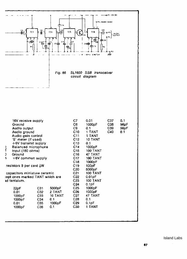
Fig.66 SL1600 SSB transceiver circuit diagram
16V receive supply C7 0.01 C37 Ground C8 1000pF C38 Audio output C9 0.1 C39 Audio ground C10 1 TANT C40 Audio gain control C11 1 TANT 'S' meter (if used) C12 10 TANT +6V transmit supply C13 0.1
} Balanced microphone C14 1000pF input (180 ohms) C15 100 TANT
0 Ground C16 47 TANT 1 +6V common supply C17 100 TANT
C18 1000pF resistors 5 per cent iW C19 100pF
C20 5000pF capacitors miniature ceramic C21 100 TANT
:ept ones marked TANT which are C22 0.01pF id tantalum. C23 100 TANT
C24 0.1pF 22pF C31 5000pF C25 1000pF 0.01 C32 2 TANT C26 1000pF 1000pF C33 10 TANT C27 47 TANT 1000pF C34 0.1 C28 0.1 0.01 C35 1000pF C29 0.1pF 1000pF C36 0.1 C30 1 TANT
0.1 56pF 56pF 0.1
67
Island Labs
68
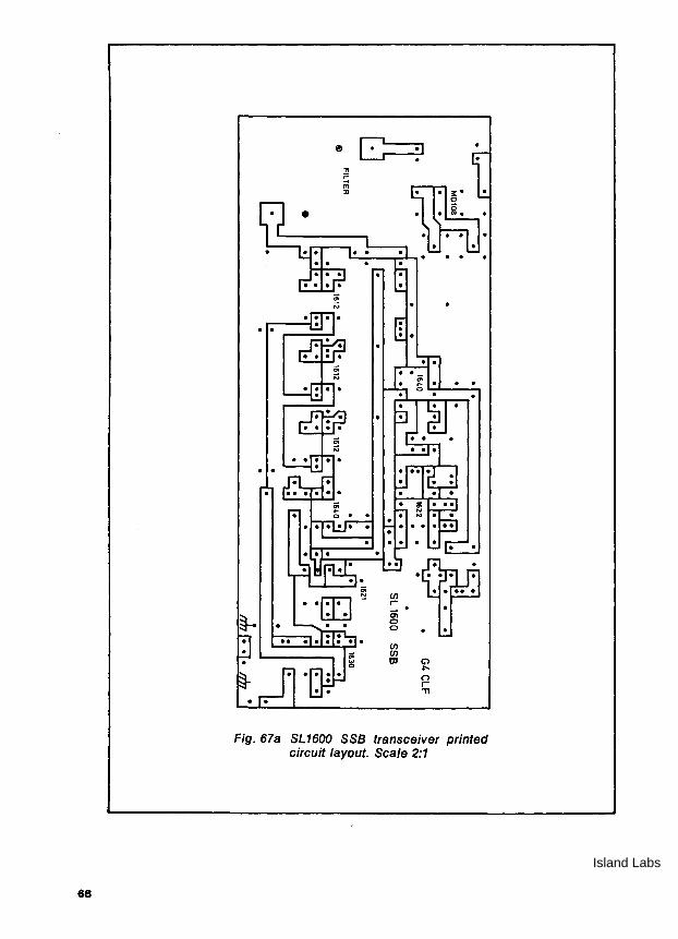
Fig.67a SL1600 SSB transceiver printed circuit layout. Scale 2:1
Island Labs
Cl ~ U
j Q..
I-Z W Z 0 Q.. ::::E 0 U
ZQ.. Q..Z
N ZQ.. ~ .... <0 I- 00
- ~~ ~ ~~
u[D (I) •
W •
g =>u. 0-I ooW
Z 0<t Z-, <tQ..
000 ZZW =>=>00 OO=> ~~
ClCl~
~UJO <t;:~ XOO
0-(1)
000 UJ WW ::<:0-0 ~u-<tUJOO ::::Ez
ZUJ 000-' UJU(l) -' => OWO IIDO
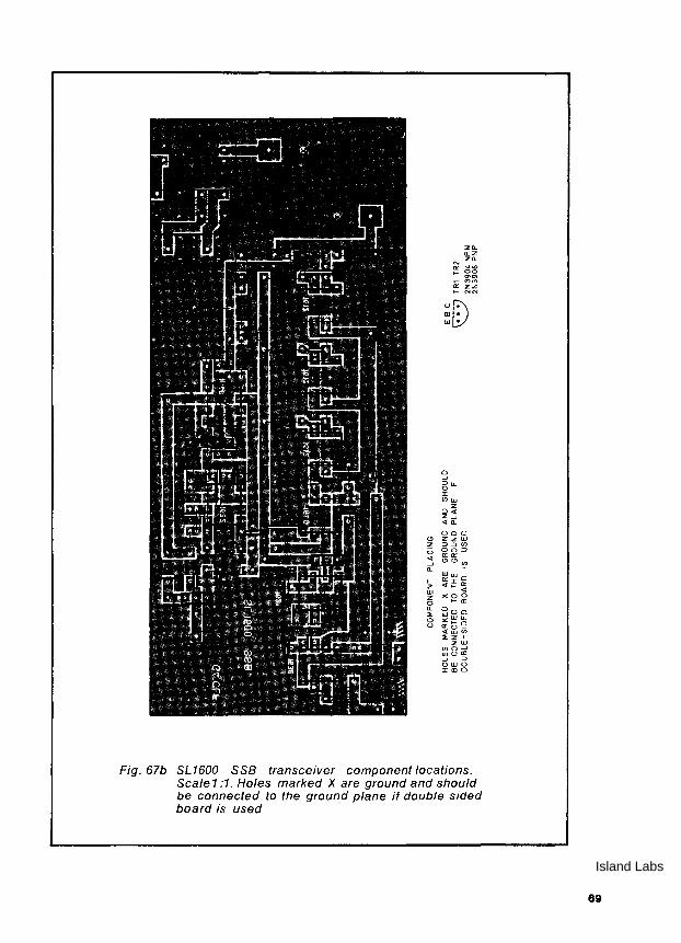
Fig. 67b SL1600 SSB transceiver component locations. Scale 1 :1. Holes marked X are ground and should be connected to the ground plane if double sided board is used
89
Island Labs
70
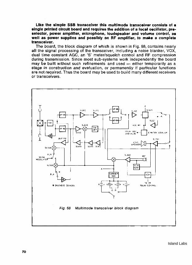
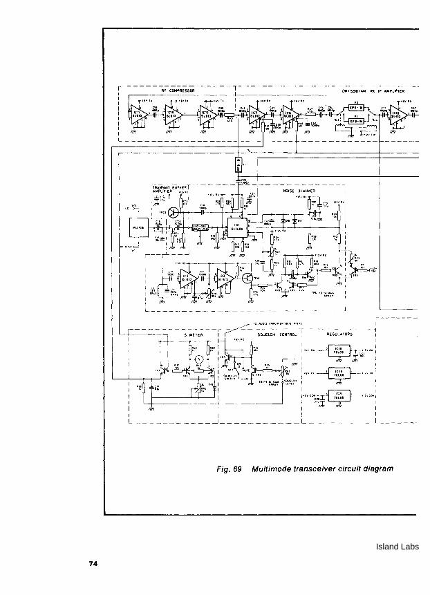
Like the simple SSB transceiver this multi mode transceiver consists of a single printed circuit board and requires the addition of a local oscillator, preselector, power amplifier, microphone, loudspeaker and volume control, a. well as power supplies and possibly an RF amplifier, to make a complete transceiver.
The board, the block diagram of which is shown in Fig. 68, contains nearly all the Signal processing of the transceiver, including a noise blanker, VOX, dual time constant AGe, an'S' meter/squelch control and RF compression during transmission. Since most sub-systems work independently the board may be built without such refinements and used - either temporarily as a stage in construction and evaluation, or permanently if particular functions are not required. Thus the board may be used to build many different receivers or transceivers.
* DISCRETE DEVICES
SL622
LOUD SPEAKER
'------tVOx
TO TR RELAY CONTROL
Fig. 68 Multimode transceiver block diagram
Island Labs
RECEIVER DESIGN CONSIDERATIONS
The major problem of receiver design is that of strong signal handling during weak signal reception. There is no si ngle cure for it but designs of high performance receivers usually have as little RF gain as possible, followed by a mixer with good strong signal performance followed at once by a crystal filter. The crystal filter removes the majority of unwanted signals and the rest of the receiver is unlikely to be troubled by them.
The crystal filters do not follow the mixer directly in this receiver, for two reasons: first, to improve the impedance match between the mixer and the filter, and secondly to permit the use of a noise blanker to suppress impulse interference.
A suitable mixer for high performance receivers must have low noise, as little conversion loss as possible, and be able to handle strong unwanted signals without intermodulation.ln this transceiver (as a reasonable compromise between cost and performance) a hot carrier diode ring mixer, the MO-108 has again been chosen. Such ring mixers perform best when they are terminated in 50 ohm resistive loads at all ports, but the input impedance of crystal filters, besides being generally higher than 50 ohms, is reactive at frequencies away from the filter passband.
In the Simple SSB Transceiver a transformer matching system was used between the mixer and the filter and the reactive mismatch was ignored. In this system a buffer amplifier, which is in fact also part of the noise blanker, is used to terminate both the mixer and the filter correctly.
A major reason for the failure of receivers to produce weak AM and SSB signals is man-made noise, typically ignition interference, at the antenna. This noise is frequently in the form of very narrow pulses of very high amplitude which can cause the crystal filter to ring at its resonant frequency. Once the filter has been thus stimulated it will stretch the pulse so that it cannot be distinguished from the wanted signal, which it swamps. Only by stopping the ignition pulse before it reaches the filter can this interference be suppressed. The noise blanker must therefore be somewhere in the receiver before the crystal filter and the best place is between the mixer and the filter.
After the crystal filters the receiver design is quite conventional. There are two filters, each feeding its own IF strip. One has a 12kHz passband and feeds the FM IF system, which is a double conversion system with a 455kHz second IF and a quadrature detector. This receiver was designed before the introduction of the SL665, which would allow the use of a single 9MHz IF.
The other fmer has a 2.4kHz passband and its output goes to the CW/SBBI AM IF strip. This strip has a broadband gain of about 70dB followed by another crystal filter, which is of 2.4kHz bandwidth for AM and SSB and 500Hz for CWo There is then another IF amplifier stage followed by two detectors. For SSB and CW there is a product detector and for AM there is an envelope detector.
On AM the envelope detector provides carrier AGC to the system but on CW and SSB an audio derived AGC system is used. Squelch and'S' meter signals are derived from the AGC line.
The decision to use a 2.4kHz filter for AM, removing one sideband, was taken on cost grounds, as was the decision to use only one 500Hz CW filter halfway down the IF strip, whereas two such filters, one at the input to the strip, would certainly improve strong Signal rejection in the CW mode. Ideally
71
Island Labs
72
there should be four filters at the input (with bandwidths of 12, 6, 2.4 and O.5kHz respectively for NBFM, AM SSB and CW) and a further three filters halfway down the AM/SBB/CW IF strip to reduce IF noise to a minimum. This would entail an extra three expensive crystal filters compared with the present system - for only a marginal increase in system performance.
The use of two filters halfway down the IF strip is well justified, however. The CW filter in this position removes both unwanted CW signals in the 2.4 kHz passband and also much of the broadband noise which can cause difficulty in copying very weak signals. The 2.4kHz filter is essential to remove the broadband noise between 100kHz and 30MHz generated by the first two IF stages which, if allowed into the AM diode detector, would greatly degrade its performance.
The improvement due to this filter on the SSB product detector is much less, since product detectors produce supersonic outputs from broadband noise and these can be filtered without loss of wanted signal. There is nevertheless a 3dB improvement in SIN ratio in systems where IF noise is the limiting factor on system performance.
TRANSMITTER DESIGN CQt.!SIDERATIONS The transmitter has to generate all the modes that the receiver has to
receive. This is not particularly difficult, but several complexities have been introduced to minimise spurious outputs and broadband noise while making the transmitter as effective as possible.
The modulation envelope of SSB does not resemble the audio producing it and normal audio speech processing techniques do not greatly improve the SIN ratio at the receiver. RF clipping, however, reduces the peak/mean power ratio of the signal and hence improves its mean power and readability.
It is also convenient to use the RF clipper for NBFM and AM, these signals being demodulated from clipped SSB back to audio and the audio signal applied to the NBFM or AM modulators. This technique gives up to 12dB apparent signal to noise ratio improvement and the resulting received audio, while obviously 'processed', is not unpleasant.
The audio input to the transmitter passes through an audio preamplifier with AGe to ensure a roughly constant modulation signal regardless of microphone or audio level. It is converted to DSB in a double-balanced modulator and filtered to SSB which is then applied to a limiting amplifier which removes all amplitude variations. This clipped signal is, of course, rich in both harmonics and intermodulation products and must be filtered in a 2.4kHz bandwidth filter to remove them. The quality of this filter determines the spectral purity of the resulting clipped SSB and is more important than the first filter producing the sideband.
The 2.4kHz bandwidth filter reintroduces amplitude variations into the Signal which must be amplified by a linear amplifier. The signal is then either further amplified and mixed to the final transmitter frequency or demodulated to yield processed audio which can be applied to the AM or FM modulators.
The FM system uses this audio to modulate the external VFO while the transceiver board supplies a steady 9MHz output to the transmitter mixer. The AM modulator - which also supplies this unmodulated carrier during FM transmission - consists of a double-balanced modulator with deliberate carrier leak. All trans'mitted signals pass through a 12kHz filter as they leave the board - this costs nothing since the filter is already present in the FM receiver,
Island Labs
and removes any broadband noise which the buffer amplifiers may have introduced.
The CW transmitter uses the complete SSB system except that a keyed tone is used as the audio input and the 500Hz filter is used instead of the 2.4kHz filter in the SSB generator. This allows only a single frequency to go to the RF clipper, rather than the several frequencies caused by harmonics from the tone generator, which would result from the use of the 2.4kHz filter.
Like the simple SSB transceiver the majority of the transmit/receive switching is performed by switching power supplies and not signal lines. The power switching itself, however, is performed by a relay which can be driven either from a transmit/receive switch or by the VOx. system. Mode switching, however, is performed by relays, so that when the transmitter and receiver are in different modes some relays change state between transmission and reception.
TRANSCEIVER SYSTEMS
To use the transceiver board it is built into a system very similar to that used for the Simple SSB Transceiver illustrated in Fig. 65. A small difference is that if FM transmission is required provision must be made for the processed audio from the board to modulate the VFO. Otherwise the two systems are identicalexcept that rather more power supplies and function switching are required with the multi mode transceiver.
Sub-systems may be omitted if a simple transceiver, or just a receiver, is required. Similarly, the board may be built and operated as an SSB receiver, then expanded to an SSB transceiver without RF clipping, then RF clipping added, etc., as required.
CIRCUIT DETAILS
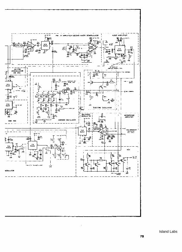
The circuit diagram of the complete transceiver board is shown in Fig. 69. The whole circuit will be described but where sub-systems are built entirely of SL600 devices conventionalty used no explanation of circuit configuration will be given. If this is required the reader is referred to Section 1.
The sub-systems into which the board has been divided are described below.
The Mixer
The Anzac MD-10B mixer was chosen for its performance coupled with its low price, but any hot carrier diode ring modulator with 50 ohm ports and adequate strong signal performance (the MD-108 will handle over 200mV RMS adjacent channel Signal) combined with low noise and under 7dB conversion loss could be used euqally well. The MD-108 has two ports with 5-500MHz bandwidth and one with DC to 500MHz bandwidth. If the transceiver is used with signals or VFO of under 5MHz it is important to ensure that this signal is appl ied to the correct port.
It might be thought that the receiver performance on strong signals would be improved by using a better diode ring, able to handle larger signals. This is not in fact so: if the mixer is imp.roved the noise blanker and filter become the limiting factors in the strong signal performance. A mixer with better high or low frequency performance may, however, be substituted if required.
73
Island Labs
74
I ~~~= I I L ___________________________ _
.,Zv F.
10A.UDIOAWtl'I(RIICI!!IPIN1i I
- - - -- -- - - - -S~~~E; - -:- - - - ~a~E~ ~;T~L-I - - - R-;G~;;O~ --- -- 1
UVA:x I ----- I
Fig. 69 Multimode transceiver circuit diagram
Island Labs
I L _____________ _
--AM/Sss- l OEMODULA TOR I
AM AGC I I
I I I I
'~+-"""""''-4+';;; I I I
-----{ I I I I I I
SSB AGe I _______ ..J
IoIOOULATOR
I---------------~
I I I I I I I \
I I I I I I I I I
: F+~'l:'y. "L'~: J; ~~., I +12'." CARRIER OSCILLATOR LU~ __ ..'.: ___________ r-J
i
unl·n SLJOIC
.. ""loY
lO:.~~'::~~NCE I Nle IN~U' I
I I I
I ____ -.J
VOX I I I
TOlf" I "ElA'1
75
Island Labs
76
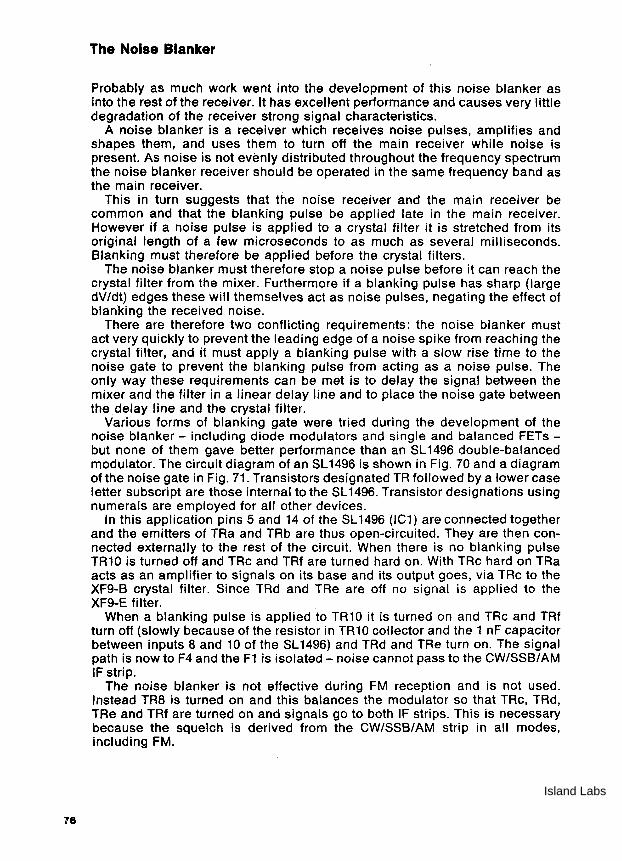
The Noise Blanker
Probably as much work went into the development of this noise blanker as into the rest of the receiver. It has excellent performance and causes very little degradation of the receiver strong signal characteristics.
A noise blanker is a receiver which receives noise pulses, amplifies and shapes them, and uses them to turn off the main receiver while noise is present. As noise is not evenly distributed throughout the frequency spectrum the noise blanker receiver should be operated in the same frequency band as the main receiver.
This in turn suggests that the noise receiver and the main receiver be common and that the blanking pulse be applied late in the main receiver. However if a noise pulse is applied to a crystal filter it is stretched from its original length of a few microseconds to as much as several milliseconds. Blanking must therefore be applied before the crystal filters.
The noise blanker must therefore stop a noise pulse before it can reach the crystal filter from the mixer. Furthermore if a blanking pulse has sharp (large dV/dt) edges these will themselves act as noise pulses, negating the effect of blanking the received noise.
There are therefore two conflicting requirements: the noise blanker must act very quickly to prevent the leading edge of a noise spike from reaching the crystal filter, and it must apply a blanking pulse with a slow rise time to the noise gate to prevent the blanking pulse from acting as a noise pulse. The only way these requirements can be met is to delay the signal between the mixer and the filter in a linear delay line and to place the noise gate between the delay line and the crystal filter.
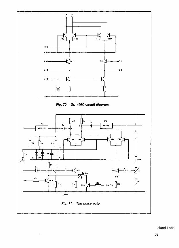
Various forms of blanking gate were tried during the development of the noise blanker - including diode modulators and single and balanced FETs -but none of them gave better performance than an Sl1496 double-balanced modulator. The circuit diagram of an Sl1496 is shown in Fig. 70 and a diagram of the noise gate in Fig. 71. Transistors designated TR followed by a lower case letter subscript are those internal to the Sl1496. Transistor designations using numerals are employed for all other devices.
In this application pins 5 and 14 of the Sl1496 (IC1) are connected together and the emitters of TRa and TRb are thus open-circuited. They are then connected externally to the rest of the circuit. When there is no blanking pulse TR10 is turned off and TRc and TRf are turned hard on. With TRc hard on TRa acts as an amplifier to signals on its base and its output goes, via TRc to the XF9-8 crystal filter. Since TRd and TRe are off no signal is applied to the XF9-E filter.
When a blanking pulse is applied to TR10 it is turned on and TRc and TRf turn off (slowly because of the resistor in TR10 collector and the 1 nF capacitor between inputs 8 and 10 of the Sl1496) and TRd and TRe turn on. The signal path is now to F4 and the F1 is isolated - noise cannot pass to the CW/SSB/AM IF strip.
The noise blanker is not effective during FM reception and is not used. Instead TR8 is turned on and this balances the modulator so that TRc, TRd, TRe and TRf are turned on and signals go to both IF strips. This is necessary because the squelch is derived from the CW/SSB/AM strip in all modes, including FM.
Island Labs
12
10o-----1-------r-------~
14o-----~----~~------------------~-------
Fig.70 SL1496C circuit diagram
In F4
L_. J XF9-E t------- _____ +-_ r--"l ..... _---'
Fig. 71 The noise gate
77
Island Labs
78
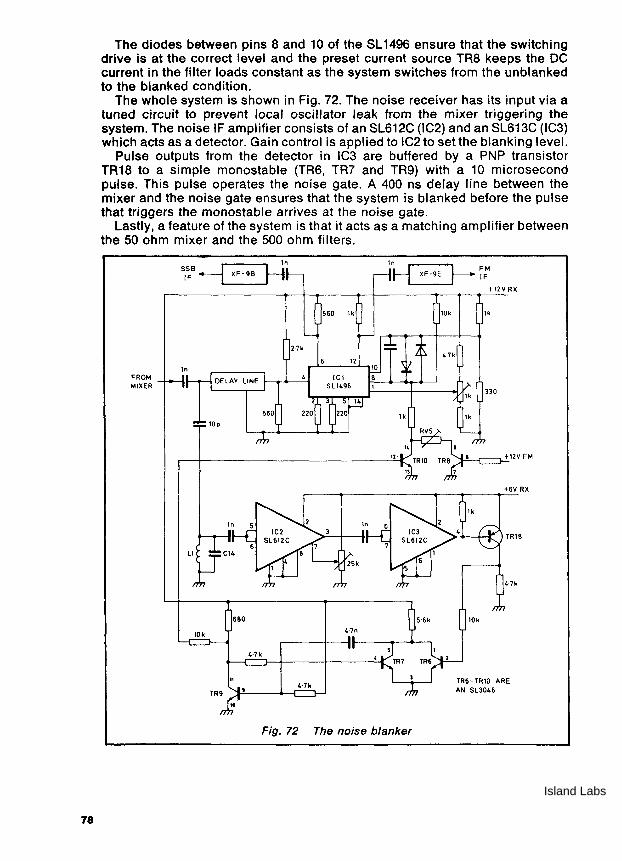
The diodes between pins 8 and 10 of the SL 1496 ensure that the switching drive is at the correct level and the preset current source TR8 keeps the DC current in the filter loads constant as the system switches from the unblanked to the blanked condition.
The whole system is shown in Fig. 72. The noise receiver has its input via a tuned circuit to prevent local oscillator leak from the mixer triggering the system. The noise IF amplifier consists of an SL612C (IC2) and an SL613C (IC3) which acts as a detector. Gain control is applied to IC2 to set the blanking level.
Pulse outputs from the detector in IC3 are buffered by a PNP transistor TR18 to a simple monostable (TR6, TR7 and TR9) with a 10 microsecond pulse. This pulse operates the noise gate. A 400 ns delay line between the mixer and the noise gate ensures that the system is blanked before the pulse that triggers the monostable arrives at the noise gate.
Lastly, a feature of the system is that it acts as a matching amplifier between the 50 ohm mixer and the 500 ohm filters.
SISFB~ _-! XF-9B
4·7k
Fig. 72
lnH LFIFM XF-9E, -
The noise blanker
t12V RX
10k
TR6- TRIO ARE AN SL3046
Island Labs
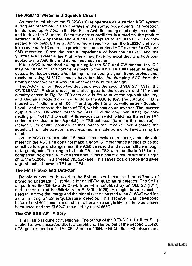
The AGC AS' Meter and Squelch Circuit
As mentioned above the SL623C (IC14) operates as a carrier AGC system during AM reception. It also operates in the same. mode during FM reception but does not apply AGC to the FM IF, the AGC line being used only for squelch and to drive the 'S'meter. When the carrier oscillator is turned on, the· product detector in IC14 operates and a signal is applied to an SL621C (IC12) connected to its output. The SL621 C is more sensitive than the SL623C and so it takes over as AGC source to provide an audio derived AGC system for CW and SSB reception. Since the output impedance of both the SL621C and the SL623C AGC systems are high when they have no input they are both connected to the AGC line and do not load each other.
If fast AGC is required during tuning in the SSB and CW modes, the ICI2 may be turned off and control restored to the IC14. This will result in higher outputs but faster decay when tuning from a strong signal. Some professional receivers using SL621C circuits have facilities for dumping AGC from the timing capacitors but it was felt unnecessary to this design.
The AGC line from these two devices drives the second SL612C (IC8) in the CW/SSB/AM IF strip directly and also goes to the squelch and'S' meter circuitry shown in Fig. 73. TR3 acts as a buffer to drive the squelch Circuitry, and also as a diode drop (O.7V) to delay the AGC to IC7. The output of TR3 is filtered by 1 kilohm and 100 nF and applied to a potentiometer ('Squelch Level') and thence to the base of TR4, which acts as an inverter. The inverter output drives TR5 which mutes the SL630C audio amplifier (IC15), by connecting pin 7 of IC15 to earth. A three-position switch which earths either TR4 collector (to disable the Squelch) or TR5 collector (to mute the receiver) is included. Its centre position neither mutes the receiver nor disables the squelch. If a mute position is not required, a single pole onloff switch may be used.
As the AGC characteristic of SL600s is somewhat non-linear, a simple voltmeter on the AGC line does not make a good'S' meter since it tends to be too sensitive to signal changes near the AGC threshold and not sensitivie enough to large signals. The long-tailed pair TR1 and TR2 with the diode 012 form a compensating circuit. All five transistors in this block of Circuitry are on a single chip, the SL3046, in a 14-lead DIL package. This saves board space and gives a good match between TR 1 and TR2.
The FM IF Strip and Detector
Double conversion is used in the FM receiver because of the difficulty of providing adequate 'a' at 9MHz for an NBFM quadrature detector. The 9MHz output from the 12kHz-wide XF9-E filter F4 is amplified by an SL612C (IC17) and is then mixed to 455kHz in an SL640C (IC20). A single tuned circuit is used to remove the image and the signal is then passed to an SL624C working as a limiting amplifier/quadrature detector. This receiver was developed before the SL665 became available - otherwise a single 9MHz filter would have been used and the SL624C replaced by an SL665C.
The CW SSB AM IF Strip
The IF strip is quite conventional. The output of the XF9-B 2.4kHz filter F1 is applied to two cascaded SL612C amplifiers. The output of the second SL612C (IC8) goes either to a 2.4kHz XF9-A or to a 500Hz XF9-M filter, (F3), depending
79
Island Labs
80
on whether the receiver is in SSB/AM or in CW mode. The filters are switched by two small relays. After the filter there is another SL612C (IC12) and an SL623C detector (IC14). Without a carrier oscillator IC14 acts as an envelope detector for AM and generates carrier-derived AGC in this mode. When the carrier oscillator is applied IC14 acts as a product detector for SSB and CW and an SL621 C (IC12) at the product detector output takes over the AGC. The audio output line must be switched between the two detectors.
012 IN914
TO IC15 ISL 630}
MUTE
TRS
I)
MUTE
TRI - TR5 ARE AN SL3046 (IC 20)
TO fiRST SL 612 AGC
L ACG fROM SL621C AND SL623C
Fig. 73a AGe "s" meter and squelch circuit
TO vox
100
+12V COM
0·1j1 470k
~----------------~~~--~~TO le4 (SL622)
Fig. 73b Sidetone oscillator
TR16 AND TR17 ARE AN SL301 ARRAY
Island Labs
The Carrier Oscillator
The carrier oscillator has four different frequencies: 8545kHz for the second mixer in the FM IF system, 8998.5kHz for USB, 9001.5KHz for LSB and 9001 kHz for CWo The circuit is a conventional FET Colpitts oscillator (TR19) and uses diode switching to select one of four crystals.
The output of the oscillator is about 1 volt RMS and is therefore reduced in a potentiometer to the 200mV RMS required by SL640Cs. This potentiometer acts as a virtually constant load to the oscillator and an output buffer is not required.
If the crystals used do not oscillate at their nominal frequency, either the two 47pF capacitors between gate and source and source and ground may be changed in value while remaining equal. Alternatively, where only one or two crystals need trimming, provision is made for crystal trimming by a varicap and a potentiometer for each sideband crystal.
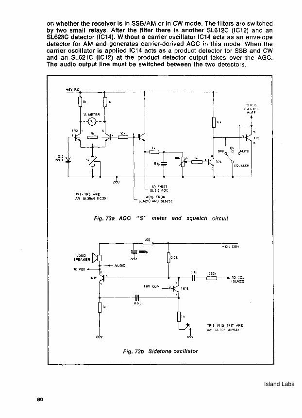
The Audio Amplifier and Sidetone Oscillator
The SL630C audio amplifier (IC15) is driven from a + 12V line. It is capable of providing up to 200mW to a small loudspeaker but if a greater output is necessary an additional audio amplifier should be provided. The output of the SL630C is also applied to the VOX circuitry, TR11 to TR15. Gain is controlled by a voltage applied to pin 8 of IC15.
Since the output impedance of the SL630C is quite high when it is turned off, and likewise that of the sidetone oscillator, the loudspeaker is connected directly to both. The sidetone oscillator shown in Fig. 73, is an emitter-coupled multivibrator keyed in the emitter of TR16. A signal is taken from the collector of TR17 and applied to the transmitter audio input.
The sidetone frequency is 1kHz and the system relies on the CW filter to produce a single tone output from the transmitter. If the 500Hz CW filter is omitted the frequency should be raised to about 1750Hz to place the second harmonic well down the SSB filter characteristic. In amateur transceivers an accurate 1750Hz may have an additional use as a repeater access tone.
The Microphone Amplifier and SSB Generator
The audio from the microphone (or the CW from the sidetone oscillator) is amplified by an SL622C (IC4). The SL622C contains its own AGC circuitry with fast attack and slow decay so that its output is around 100mV RMS for over 60dB range of input. There is also a sidetone output which is not affected by the AGC and is used to operate the VOX. R57 sets the microphone AGC threshold and dynamic range. If R57 is open circuit, the threshold is 100 microvolts and the dynamic range is 60dB; if it is 1 kilohm the values are 1mV and 40dB, and if it is 330 ohms they are 3mV and 30dB. C63 should be increased to 0.05 microfarad if R57 is 1 kilohms and to 0.15 microfarad if it is 330 ohms.
The output from the SL622C is applied to the signal input of an SL640C double-balanced modulator (IC9) whose carrier input is 8.9985 MHz or 9.0015 MHz from the carrier oscillator. The output is DSB which is applied to the 2.4kHz bandwidth 9MHz filter (F2) and one sideband removed to produce SSB (USB if 8.9985 MHz is used, LSB if 9.0015).
81
Island Labs
82
The RF Compressor
The SSB produced in the system above is normal SSB. Its peak/mean power ratio is fairly large, even though its mean power level is quite constant as a result of the audio AGC. It is therefore amplified in a three-stage amplifier consisting of an SL610C (IC11) followed by two SL613Cs (IC10 and IC13). The SL610C is merely to provide gain but the SL613Cs are high performance limiting amplifiers with symmetrical limiting. The signal emerging from this limiting amplifier preserves its phase information but has had practically all amplitude variation removed from it.
Such a clipped signal is rich in both harmonics and intermodulation products, so it is immediately filtered in another 2.4kHz bandwidth filter (F1) which removes both, but reintroduces some amplitude variation.
The above system is used to process all signals which are to be transmitted, in whatever mode the transmitter is operating. However if a CW signal is being sent, the first 2.4kHz filter (F2) is replaced with a 500Hz filter (F3) to ensure that a single tone is applied to the clipper. After the second filter, however, different modes are processed in different ways.
Single-sideband and CW signals are ampl ified in a two stage linear amplifier, applied to a 12kHz filter to remove noise and sent to the mixer via the transmit buffer.
When the transmitter is operating in AM or FM mode the clipped SSB is demodulated in an SL640C product detector (IC6) to yield clipped audio, which is then applied to the AM or FM modulators. The SSB clipping produces audio with a slightly artificial sound which, however, is not unpleasant under strong signal conditions, and is particularly easy to copy through noise.
The AM modulator is another SL640C (IC5) with carrier leak deliberately introduced so that the output is AM rather than suppressed carrier DSB. This modulator is used both in the AM and FM modes, but in the FM mode no Signal is applied to the Signal input and the output is an unmodulated carrier. In either case the output is amplified, filtered in the 12kHz filter (F4), and sent to the transmitter via the transmit buffer and the mixer.
In FM mode the circuit transmits an unmodulated carrier. Frequency modulation is performed off the board by using the processed audio to modulate the transceiver VFO during transmission.
The carrier on AM and FM is not, as one might expect, 9MHz. There is only one carrier oscillator on the board and it is used during transmission to produce Clipped SSB. It is therefore working at 9001.5kHz or 8998.5kHz, depending on the position of the sideband selector. The AM or FM carrier is at the same frequency.
The Buffer Amplifiers
The buffer amplifiers used between the various parts of the transmitter are simple transistor or FET circuits. The first designs of the transceiver used integrated circuits to perform these functions but this led to unnecessary complexity and cost with no corresponding increase in performance.
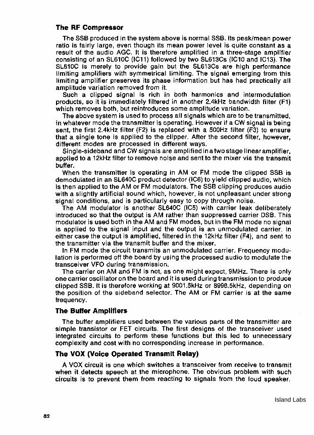
The VOX (VOice Operated Transmit Relay)
A VOX circuit is one which switches a transceiver from receive to transmit when it detects speech at the microphone. The obvious problem with such circuits is to prevent them from reacting to signals from the loud speaker.
Island Labs
FROM 10}!
LOUD ----11 SPEAKER
TR12 - TR15 ARE
AN SL3046
1-8k
+ c::; 20p
lOp
+12'1 COMMON
TO RELAY ~-......-..... DRIVER
TR15
')
n+ FROM IC4 (SL 622) Uf-'---- AUX. OUTPUT
Fig. 74 VOX circuit
The simplest way to do this is to feed the loudspeaker signals to the VOX circuit so that only microphone signals which are not also present in the loudspeaker circuit affect its operation. This is quite difficult and is often liable to cause spurious switching unless the system is carefully adjusted by the operator to compensate for the microphone and the acoustics of the surroundings.
The system used in this transceiver is slightly different. The signal from the microphone is gated by the internal signal to the loudspeaker so that no input to the microphone will affect the VOX while there is a signal to the loudspeaker. The only drawback to this system is that the VOX cannot operate during the reception of non-syllabic noise. Such conditions are, however, unusual.
The circuit is shown in Fig. 74 and uses another SL3046 five transistor monolithic array. Positive half-cycles from the microphone amplifier SL622C (which is powered during reception} turn on TR13 unless prevented by the presence of a loudspeaker signal on TR11. The time constant of the gate circuit is such that VOX action can occur in the spaces between words in normal speech.
TR13 turns on TR15 via TR14. An integrator consisting of R61 and C98 controls the time which elapses between the cessation of speech and the reversion to reception. For breakthrough CW operation (when the operator listens between the dots and dashes of his own transmission) the time constant may be reduced. If the relay is a low power one it may be connected between TR15 collector and + 12V, otherwise a PNP driver should be used with an input resistor in its base circuitry.
Power Supplies and Switching
The transceiver board uses three + 12V supplies. One is present during reception, one during transmission, and one is common. There are three +6V integrated circuit regulators on the board, one for each + 12V line, to supply the appropriate SL600s. This type of regulation greatly reduces crosstalk via the supplies.
Mode switching is accomplished by applying + 12V to the relevant one of the three mode lines: CW, FM, or SSB. The two unwanted lines are earthed.
83
Island Labs
84
Construction The transceiver board is constructed of double-sided printed circuit material
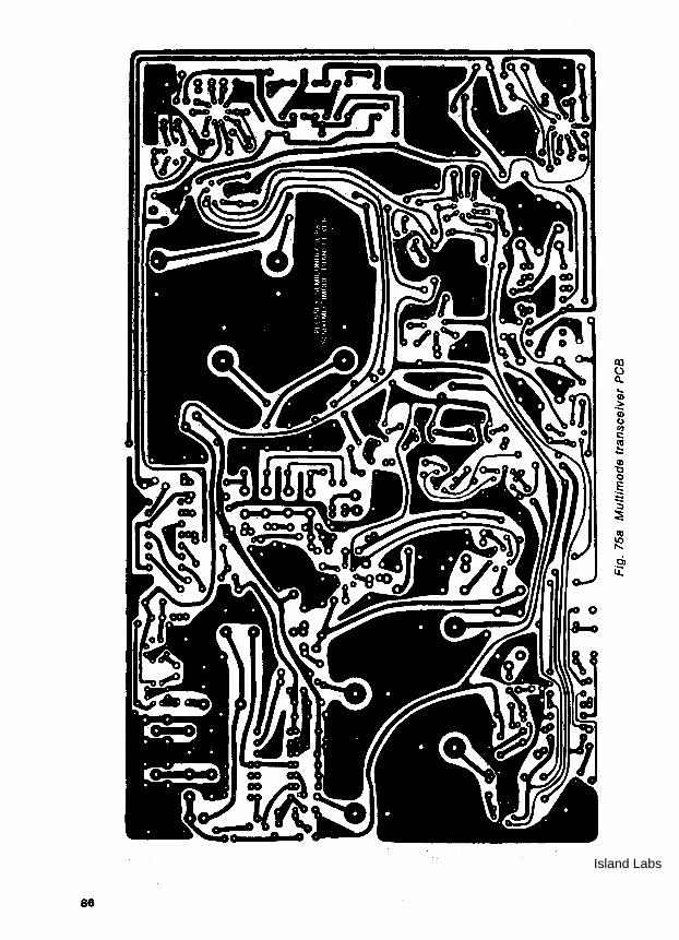
and earth connections are made on both sides of the board - plated through holes would remove this necessity but were not used in the prototype for reasons of cost and ease of modification. As the board is very small for the complexity of circuitry it carries some of the relay connections were wired. The board diagram is Fig. 75a and the component location is given in Fig. 75b.
It would be almost impossible to make such a system stable on singlesided board but systems derived from this one and built on double-sided board should not present any particular layout problems. Table 5 Components for the multimode transceiver (Fig. 69)
INTEGRATED R23 33K VARIABLE RESISTORS C39 1000pF CIRCUITS R24 4.7K RVl 10K C40 1000pF
R25 1K RV2 1K C41 0.1~F ICl SL 1496 R26 2.7K RV3 lK C42 4700pF IC2 SL612C R27 1K RV4 1K C43 1000pF IC3 SL613C R28 330 RV5 10K C44 1000pF IC4 SL622C . R29 10K RV6 5K Lin.(NOB) C45 220pF IC5 SL640C R30 560 RV7 10K lin. (NOB) C46 50pF IC6 SL640C R31 10K RV8 25K lin. (NOB) C47 O.ljJF IC7 SL612C R32 560 C48 1000pF IC8 SL612C R33 lK CAPACITORS C49 4700pF IC9 SL640C R34 10K Cl 47p C50 0.01jJF IC10 SL613C R35 lK C2 O.ljJF C51 O.ljJF IC11 SL610C R36 1K C3 0.1jJF C52 100IJF(T) IC12 SL621C R37 10K C4 47pF C53 O.1jJF IC13 SL613C R38 lK C5 0.1jJF C54 1000pF IC14 SL623C R39 1K C6 0.1jJF C55 0.1lJF IC15 SL630C R40 1K C7 O.ljJF C56 1000pF IC16 SL612C R41 1K C8 4700pF C57 0.11JF IC17 SL612C R42 4.7K C9 0.1jJF C58 10pF IC18 78106 R43 330 C10 O.1IJF C59 1.0pF IC19 78106 R44 100 Cl1 1000pF C60 1000pF IC20 Sl640C R45 470 C12 O.ljJF C61 O.ljJF IC21 78L06 R46 100 C13 10pF C62 10jJF(T) IC22 SL624 R47 470 C14 100pF C63 4700pF
R48 1K C15 1000pF C64 330pF RESISTORS (ohms) R49 10K C16 O.ljJF C65 1000pF Rl 470(NOB) R50 10K e17 l000pF C66 1000pF R2 100(NOB) R51 82 C18 1000pF C67 1000pF R3 56K R52 10 C19 O.ljJF C68 1jJF(T) R4 100 R53 560 C20 1000pF C69 47jJF(T) R5 47K R54 1K C21 0.1jJF C70 0.1jJF R6 lK R5S lK C22 1000pF C71 1000pF R7 10K R56 2.2K C23 1000pF C72 100jJF(T) R8 5.6K R57 See text C24 O.1jJF C73 100J.lF(T) R9 4.7K R58 470K C25 1000pF C74 ljJF(T) R10 680 R59 lK C26 O.ljJF C75 100jJF(T) R1l 4.7K R60 lOOK C27 1000pF C76 47jJF(T) R12 10K R61 100K C28 1000pF cn O.OljJF(T) R13 1K R62 1.8K C29 1000pF (;78 100jJF(T) R14 10K R63 15K C30 ljJF(T) C79 0.1jJF R15 4.7K R64* lK C31 1000pF cao 1J,1F(T) R16 lK R65* lK C32 O.ljJF C81 4700pF R17 220 R66 4.7K(NOB) C33 1000pF C82 100pF R18 220 R67t 15K C34 10jJF(T) C83 1000pF R19 560 C35 1000pF C84 10jJF(T) R20 lK C36 0.1jJF C85 47jJF(T) R21 50 * Vertical on board C37 1000pF C86 1000pF R22 4.7K t May need selection C38 1000pF Ca7 0.5jJF(T)
Island Labs
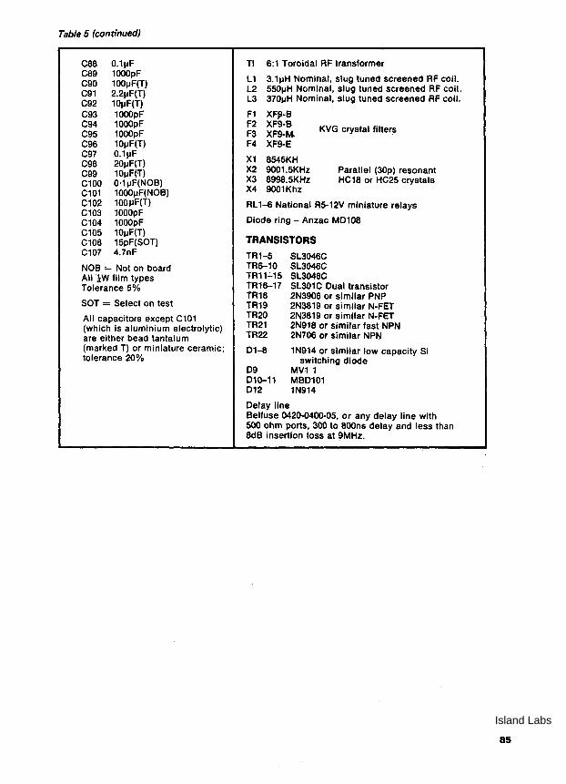
Table 5 (continued)
C88 O.l~F C89 1000pF C90 100jJF(T) C91 2.2~F(T) C92 10jJF(T) C93 1000pF C94 1000pF C95 1000pF C96 10jJF(T) C97 O.ljJF C98 20~F(T) C99 10J,lF('T) Cl00 0'1J,1F(NOB) Cl01 1000J,lF(NOB) Cl02 100IJF(T) Cl03 1000pF Cl04 1000pF Cl05 10jJF(T) Cl06 15pF(SOT) Cl07 4.7nF
NOB = Not on board All lW film types Tolerance 5%
SOT = Select on test
All capacitors except C101 (which is aluminium electrolytic) are either bead tantalum (marked T) or miniature ceramic; tolerance 20%
TI 6:1 Toroidal RF transformer
L1 3.11JH Nominal, slug tuned screened RF coil. L2 550jJH Nominal, slug tuned screened RF coil. L3 370J,lH Nominal, slug tuned screened AF coil.
Fl XF~-B F2 XF9-B F3 XF9-M. KVG crystal filters
F4 XF9-E
Xl 8545KH X2 9001.5KHz X3 8998.5KHz X4 9001Khz
Parallel (30p) resonant HC18 or HC25 crystals
RL 1-6 National A5-12V miniature relays
Diode ring - Anzac M0108
TRANSISTORS
TAl-5 TA6-l0 TAll-15 TAl6-17 TA18 TR19 TA20 TA21 TA22
01-8
09 010-11 012
Delay line
SL3046C SL3046C SL3046C SL301C Dual transistor 2N3906 or similar PNP 2N3819 or similar N-FET 2N3819 or similar N-FET 2N91S' or similar fast NPN 2N706 or similar NPN
lN914 or similar low capacity Si switching diode
MV11 MBD101 lN914
Belfuse 0420-0400-05, or any delay line with 500 ohm ports, 300 to 800ns delay and less than SdB insertion 10$s at 9MHz.
85
Island Labs
86
Island Labs
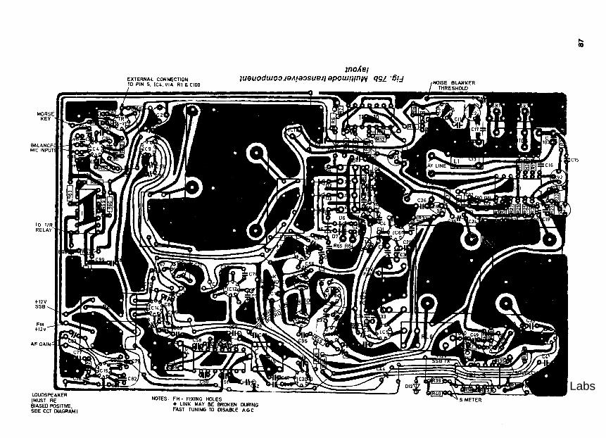
MORSE KEY
EXTERNAL CONNECTION TO PIN 5. IC4. VIA Rl & ClOD
lno,{e/ lUBUodwo:J JBA/B:JSUeJl BpOWmnw qgL ·6/::/
BALANCEJ• ~J!]JII~ MIC INPUT~C4S
TO T/ RELAY.~
+12V SSB
FM +12V
AF GAIN~"'b....\d
NOTES; FH = FIXING HOLES • LINK MAY BE BROKEN DURING FAST TUNING TO DISABLE A G C
... co
Island Labs