signal integrity, emi & crosstalk...
TRANSCRIPT

TM
Freescale Semiconductor Confidential and Proprietary Information. Freescale™ and the Freescale logo are trademarksof Freescale Semiconductor, Inc. All other product or service names are the property of their respective owners. © Freescale Semiconductor, Inc. 2008.
in High Speed Digital Circuits & PC Boards.Signal Integrity, EMI & Crosstalk Control
June 19, 2008
Rick HartleySr. Principal Engineer - L-3 Avionics Systems, Inc.

TMFreescale Semiconductor Confidential and Proprietary Information. Freescale™ and the Freescale logo are trademarksof Freescale Semiconductor, Inc. All other product or service names are the property of their respective owners. © Freescale Semiconductor, Inc. 2008. 2
Agenda - Control of SI & EMI
►Recommended Reading Lists►Electrical Domain (R, C, L, Currents, Frequency, etc.)►Er, Propagation Time/Velocity and Rise Distance►Transmission Lines and How to Resolve Impedance►Effect of Loading on Transmission Lines►Trace Routing and Termination Schemes►Signal & Wave Attenuation►Connectors and other Discontinuities►Understanding Cross Talk►Power Distribution and Decoupling►EMI - Understanding and Control►Planes and Plane Splits►PC Board Stack-ups that work

TMFreescale Semiconductor Confidential and Proprietary Information. Freescale™ and the Freescale logo are trademarksof Freescale Semiconductor, Inc. All other product or service names are the property of their respective owners. © Freescale Semiconductor, Inc. 2008. 3
High Speed Design Reading List
1. Right the First Time- A Practical Handbook on High Speed PCB and System Design - Volumes I & II - Lee W. Ritchey (Speeding Edge) - ISBN 0-9741936-0-7
2. High Speed Digital System Design- A handbook of Interconnect Theory and Practice - Hall, Hall and McCall (Wiley Interscience2000) - ISBN 0-36090-2
3. High Speed Digital Design- A Handbook of Black Magic - Howard W. Johnson & Martin Graham (Prentice Hall) - ISBN 0-13-395724-1
4.High Speed Signal Propagation- Advanced Black Magic - Howard W. Johnson & Martin Graham - (Prentice Hall) - ISBN 0-13-084408-X
5.Signal Integrity Simplified - Eric Bogatin (Prentice Hall) - ISBN 0-13-066946-6
6.Signal Integrity Issues and Printed Circuit Design - Doug Brooks (Prentice Hall) - ISBN 0-13-141884-X

TMFreescale Semiconductor Confidential and Proprietary Information. Freescale™ and the Freescale logo are trademarksof Freescale Semiconductor, Inc. All other product or service names are the property of their respective owners. © Freescale Semiconductor, Inc. 2008. 4
EMI Reading List
1.PCB Design for Real-World EMI Control - Bruce R. Archambeault(Kluwer Academic Publishers Group) - ISBN 1-4020-7130-2
2.Digital Design for Interference Specifications- A Practical Handbook for EMI Suppression - David L. Terrell & R. Kenneth Keenan (Newnes Publishing) - ISBN 0-7506-7282-X
3.Noise Reduction Techniques in Electronic Systems - Henry Ott(2nd Edition - John Wiley and Sons) - ISBN 0-471-85068-3
4.Introduction to Electromagnetic Compatibility - Clayton R. Paul (John Wiley and Sons) - ISBN 0-471-54927-4
5.EMC for Product Engineers - Tim Williams (Newnes Publishing) -ISBN 0-7506-2466-3
6.Grounding & Shielding Techniques - Ralph Morrison (5th Edition -John Wiley & Sons) - ISBN 0-471-24518-6

TMFreescale Semiconductor Confidential and Proprietary Information. Freescale™ and the Freescale logo are trademarksof Freescale Semiconductor, Inc. All other product or service names are the property of their respective owners. © Freescale Semiconductor, Inc. 2008. 5
Read Books NOT IC App Notes
“Circuit Application notes produced by IC manufacturers should be assumed Wrong until Proven
Right!”
Lee W. Ritchey

TMFreescale Semiconductor Confidential and Proprietary Information. Freescale™ and the Freescale logo are trademarksof Freescale Semiconductor, Inc. All other product or service names are the property of their respective owners. © Freescale Semiconductor, Inc. 2008. 6
Read Books NOT IC App Notes
What our industry needs!?!?!?
Source: CoilCraft

TMFreescale Semiconductor Confidential and Proprietary Information. Freescale™ and the Freescale logo are trademarksof Freescale Semiconductor, Inc. All other product or service names are the property of their respective owners. © Freescale Semiconductor, Inc. 2008. 7
PC Board Properties
►A Transmission Line is any Pair or Wires or Conductors used to Move Energy From point A to point B, Usually of Controlled Size and in a Controlled Dielectric to create a Con-trolled Impedance (Zo).

TMFreescale Semiconductor Confidential and Proprietary Information. Freescale™ and the Freescale logo are trademarksof Freescale Semiconductor, Inc. All other product or service names are the property of their respective owners. © Freescale Semiconductor, Inc. 2008. 8
PC Board Properties
►Below 1 - 2 GHz ‘R’ and ‘G’ are less significant in Digital Circuits and can be ignored.
►Therefore, at lower Frequencies -
►Notice That Zo is independent of Length.
TMFreescale Semiconductor Confidential and Proprietary Information. Freescale™ and the Freescale logo are trademarksof Freescale Semiconductor, Inc. All other product or service names are the property of their respective owners. © Freescale Semiconductor, Inc. 2008. 9
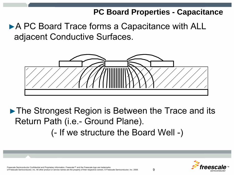
PC Board Properties - Capacitance
►A PC Board Trace forms a Capacitance with ALL adjacent Conductive Surfaces.
►The Strongest Region is Between the Trace and its Return Path (i.e.- Ground Plane).
(- If we structure the Board Well -)

TMFreescale Semiconductor Confidential and Proprietary Information. Freescale™ and the Freescale logo are trademarksof Freescale Semiconductor, Inc. All other product or service names are the property of their respective owners. © Freescale Semiconductor, Inc. 2008. 10
PC Board Properties - Inductance
►Property of the Circuit Allowing Energy Storage in a Field Induced by Current Flow.
►Field consists of Magnetic Flux Lines which Surround the Conductor.
►Energy causes Inertia to Changes in Current.►Inertia causes Frequency Dependence.

TMFreescale Semiconductor Confidential and Proprietary Information. Freescale™ and the Freescale logo are trademarksof Freescale Semiconductor, Inc. All other product or service names are the property of their respective owners. © Freescale Semiconductor, Inc. 2008. 11
PC Board Properties - Inductance
In Circuits and PC Boards there are 2 Issues we need to understand regarding Inductance:
First-►Function of Trace Length and Cross-Sectional Area
(Width x Thickness).►Decreases if Trace is Shorter, Wider, Thicker.►.020” Wide, 1 oz, 1.0” Long Trace placed very far
return path = 25 nH.►Must be Widened to 1.0” to = 12.5 nH.

TMFreescale Semiconductor Confidential and Proprietary Information. Freescale™ and the Freescale logo are trademarksof Freescale Semiconductor, Inc. All other product or service names are the property of their respective owners. © Freescale Semiconductor, Inc. 2008. 12
PC Board Properties - Inductance
Second-►Function of Closed Loop Area between the Trace
and its Return Path.►Inductance Decreases as Closed Loop Area
Decreases (Referred to as Self Inductance).►.020” Wide, 1.0” Long (25nH) Trace placed above
its Return Path (next layer plane) w/ .010”separation (trace - plane) = 6.5nH.

TMFreescale Semiconductor Confidential and Proprietary Information. Freescale™ and the Freescale logo are trademarksof Freescale Semiconductor, Inc. All other product or service names are the property of their respective owners. © Freescale Semiconductor, Inc. 2008. 13
Operating Frequency Bandwidth

TMFreescale Semiconductor Confidential and Proprietary Information. Freescale™ and the Freescale logo are trademarksof Freescale Semiconductor, Inc. All other product or service names are the property of their respective owners. © Freescale Semiconductor, Inc. 2008. 14
Operating Frequency Bandwidth
►Highest Frequency of concern IS NOT the Clock.►Is Frequency of the High Harmonics necessary to
create the Fast Rising Edges of the Signal.►Called Maximum Pulse Frequency.
F (Freq-GHz) = .50 / Tr (rise/fall time-ns *)* (Tr = 10-90% (Typical))* (Tr = 10-90% (Typical))
►Frequency Bandwidth is from Clock to Maximum Pulse Frequency.
TMFreescale Semiconductor Confidential and Proprietary Information. Freescale™ and the Freescale logo are trademarksof Freescale Semiconductor, Inc. All other product or service names are the property of their respective owners. © Freescale Semiconductor, Inc. 2008. 15
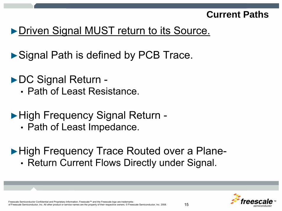
Current Paths
►Driven Signal MUST return to its Source.
►Signal Path is defined by PCB Trace.
►DC Signal Return -• Path of Least Resistance.
►High Frequency Signal Return -• Path of Least Impedance.
►High Frequency Trace Routed over a Plane-• Return Current Flows Directly under Signal.

TMFreescale Semiconductor Confidential and Proprietary Information. Freescale™ and the Freescale logo are trademarksof Freescale Semiconductor, Inc. All other product or service names are the property of their respective owners. © Freescale Semiconductor, Inc. 2008. 16
Current Paths►2 Layer Microwave Style PC Board -
L2- Ground.
L1- Routed Signal, routed Power and poured Ground copper.
Where does signal’s return current flow?

TMFreescale Semiconductor Confidential and Proprietary Information. Freescale™ and the Freescale logo are trademarksof Freescale Semiconductor, Inc. All other product or service names are the property of their respective owners. © Freescale Semiconductor, Inc. 2008. 17
Current Paths
What if the Plane is not ‘Ground’??????
►What happens if Return Plane is Split???• Now where does return current flow?
TMFreescale Semiconductor Confidential and Proprietary Information. Freescale™ and the Freescale logo are trademarksof Freescale Semiconductor, Inc. All other product or service names are the property of their respective owners. © Freescale Semiconductor, Inc. 2008. 18
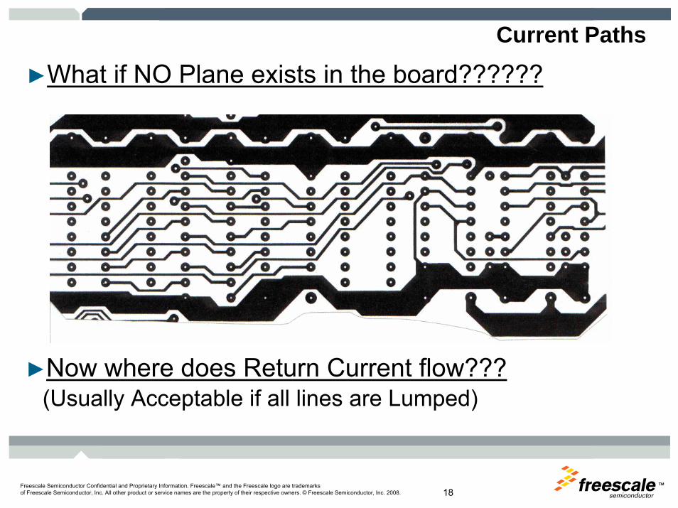
Current Paths
►What if NO Plane exists in the board??????
►Now where does Return Current flow???(Usually Acceptable if all lines are Lumped)

TMFreescale Semiconductor Confidential and Proprietary Information. Freescale™ and the Freescale logo are trademarksof Freescale Semiconductor, Inc. All other product or service names are the property of their respective owners. © Freescale Semiconductor, Inc. 2008. 19
Transmission Line Characteristics
►When do Problems begin???• When the Time to Propagate a Conductor’s Length is
Greater than 1/4 of the Signal Rise or Fall Time.
►Most extreme when Time to Propagate the Conductor’s Length is Equal to or Greater than the Signal Rise or Fall Time.

TMFreescale Semiconductor Confidential and Proprietary Information. Freescale™ and the Freescale logo are trademarksof Freescale Semiconductor, Inc. All other product or service names are the property of their respective owners. © Freescale Semiconductor, Inc. 2008. 20
Transmission Line Characteristics
Reflections -
►When a Pulse propagates a Long Transmission Line of Impedance Zo and reaches a Load of the same Impedance, ALL the energy is Transferred.
►If the ‘Down Stream’ Impedance (Zload) is different than that of the Line (Zo), then a percentage of the Pulse is Reflected back toward the Source.
TMFreescale Semiconductor Confidential and Proprietary Information. Freescale™ and the Freescale logo are trademarksof Freescale Semiconductor, Inc. All other product or service names are the property of their respective owners. © Freescale Semiconductor, Inc. 2008. 21
Transmission Line Characteristics
Relative Permittivity -
►Measure of the affect a material has on the Capacitance of a Pair of Conductors compared to the same Pair in a Vacuum
►Also, affects travel time (Propagation Time) of a signal in that Pair of Conductors.
►Relative Permittivity is expressed using Greek letter “Epsilon”, followed by lower case “r”.
(i.e.- εr or Er (aka DK (Dielectric Constant.))

TMFreescale Semiconductor Confidential and Proprietary Information. Freescale™ and the Freescale logo are trademarksof Freescale Semiconductor, Inc. All other product or service names are the property of their respective owners. © Freescale Semiconductor, Inc. 2008. 22
Transmission Line Characteristics
Relative Permittivity -
Er (εr ) of FR4 -►Frequency Dependent.
►Dependent on Glass-to-Resin Ratio.
►Materials available w/ More Constant Er-• Most Materials designed for High Speed.• All PTFE based Materials.

TMFreescale Semiconductor Confidential and Proprietary Information. Freescale™ and the Freescale logo are trademarksof Freescale Semiconductor, Inc. All other product or service names are the property of their respective owners. © Freescale Semiconductor, Inc. 2008. 23

TMFreescale Semiconductor Confidential and Proprietary Information. Freescale™ and the Freescale logo are trademarksof Freescale Semiconductor, Inc. All other product or service names are the property of their respective owners. © Freescale Semiconductor, Inc. 2008. 24
Transmission Line Characteristics
- Er of FR4 vs Frequency -
Also see Nelco and Isola Websites.

TMFreescale Semiconductor Confidential and Proprietary Information. Freescale™ and the Freescale logo are trademarksof Freescale Semiconductor, Inc. All other product or service names are the property of their respective owners. © Freescale Semiconductor, Inc. 2008. 25
6 mil line (Outer Layer - 500 MHz) = 63Ω5 mil line (Inner Layer - 500 MHz) = 61Ω
- Standard Board Stack vs Zo -

TMFreescale Semiconductor Confidential and Proprietary Information. Freescale™ and the Freescale logo are trademarksof Freescale Semiconductor, Inc. All other product or service names are the property of their respective owners. © Freescale Semiconductor, Inc. 2008. 26
6 mil line (Outer Layer - 500 MHz) = 63Ω5 mil line (Inner Layer - 500 MHz) = 56Ω
- Standard Board Stack vs Zo -

TMFreescale Semiconductor Confidential and Proprietary Information. Freescale™ and the Freescale logo are trademarksof Freescale Semiconductor, Inc. All other product or service names are the property of their respective owners. © Freescale Semiconductor, Inc. 2008. 27
Transmission Line Characteristics
Propagation Time & Velocity -
►Prop Time is a measure of Signal Travel Time per Unit of Length (i.e.- .17ns per inch).
►Prop Velocity is a measure of Signal Travel Length per Unit of Time (i.e.- 5.89” per ns).
►Prop Time & Velocity (‘Inner Layer’ Signal) -
(Where: c = Speed of Light)

TMFreescale Semiconductor Confidential and Proprietary Information. Freescale™ and the Freescale logo are trademarksof Freescale Semiconductor, Inc. All other product or service names are the property of their respective owners. © Freescale Semiconductor, Inc. 2008. 28
Transmission Line Characteristics
Propagation Time & Velocity -Effective Relative Er - Microstrip
⎥⎥⎥⎥
⎦
⎤
⎢⎢⎢⎢
⎣
⎡
⎟⎠⎞
⎜⎝⎛ −+
+
−+
+=
2
104.0121
12
12
1hw
wh
rreff
εεε 1<hw
⎥⎥⎥⎥
⎦
⎤
⎢⎢⎢⎢
⎣
⎡
⎥⎥⎥⎥
⎦
⎤
⎢⎢⎢⎢
⎣
⎡
+
−+
+=
wh
rreff 121
12
12
1 εεε
otherwiseFor Propagation of Outer layer Traces - Plug Eeff into Equa-tions on prev-ious page -OR-
If-

TMFreescale Semiconductor Confidential and Proprietary Information. Freescale™ and the Freescale logo are trademarksof Freescale Semiconductor, Inc. All other product or service names are the property of their respective owners. © Freescale Semiconductor, Inc. 2008. 29
Transmission Line Characteristics
Propagation Time & Velocity -
►The Outer Layer (Microstrip) Equivalent -
(Where: c = Speed of Light)
TMFreescale Semiconductor Confidential and Proprietary Information. Freescale™ and the Freescale logo are trademarksof Freescale Semiconductor, Inc. All other product or service names are the property of their respective owners. © Freescale Semiconductor, Inc. 2008. 30
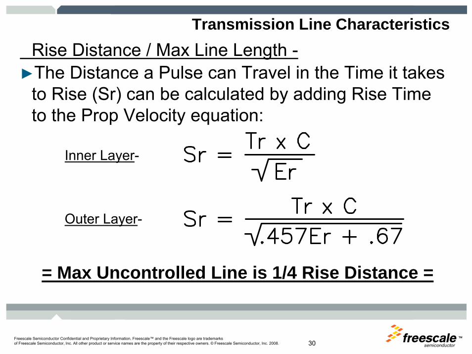
Transmission Line CharacteristicsRise Distance / Max Line Length -
►The Distance a Pulse can Travel in the Time it takes to Rise (Sr) can be calculated by adding Rise Time to the Prop Velocity equation:
= Max Uncontrolled Line is 1/4 Rise Distance =
Inner Layer-
Outer Layer-

TMFreescale Semiconductor Confidential and Proprietary Information. Freescale™ and the Freescale logo are trademarksof Freescale Semiconductor, Inc. All other product or service names are the property of their respective owners. © Freescale Semiconductor, Inc. 2008. 31
Transmission Line Characteristics
Logic Families / Rise Time / Max Line Length -Max Line Length- Max Line Length-
DEVICE TYPE RISETIME Inner (Inch/mm) Outer (Inch/mm)Standard TTL 5.0 nSec 7.27 / 185 9.23 / 235Schottky TTL 3.0 nSec 4.36 / 111 5.54 / 14110K ECL 2.5 nSec 3.63 / 92 4.62 / 117ASTTL 1.9 nSec 2.76 / 70 3.51 / 89FTTL 1.2 nSec 1.75 / 44 2.22 / 56BICMOS 0.7 nSec 1.02 / 26 1.29 / 3310KH ECL 0.7 nSec 1.02 / 26 1.29 / 33100K ECL 0.5 nSec .730 / 18 .923 / 23GaAs 0.3 nSec .440 / 11 .554 / 14
(Calculated assuming a nominal Er = 4.1)

TMFreescale Semiconductor Confidential and Proprietary Information. Freescale™ and the Freescale logo are trademarksof Freescale Semiconductor, Inc. All other product or service names are the property of their respective owners. © Freescale Semiconductor, Inc. 2008. 32
Transmission Line Impedance Calculations
- Microstrip -
Assumes LPI Soldermask over Bare Copper.

TMFreescale Semiconductor Confidential and Proprietary Information. Freescale™ and the Freescale logo are trademarksof Freescale Semiconductor, Inc. All other product or service names are the property of their respective owners. © Freescale Semiconductor, Inc. 2008. 33
- Embedded Microstrip -
Dimensions Must be in Inches-i.e.- 8 mils must be expressed as .008”.
To use other units, convert 0.1to 100 for milsto 2.54 for mmto .254 for cm
Transmission Line Impedance Calculations
TMFreescale Semiconductor Confidential and Proprietary Information. Freescale™ and the Freescale logo are trademarksof Freescale Semiconductor, Inc. All other product or service names are the property of their respective owners. © Freescale Semiconductor, Inc. 2008. 34
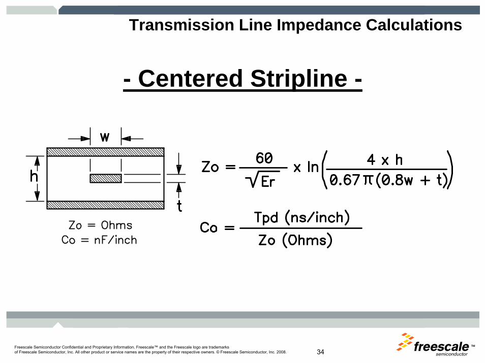
- Centered Stripline -
Transmission Line Impedance Calculations

TMFreescale Semiconductor Confidential and Proprietary Information. Freescale™ and the Freescale logo are trademarksof Freescale Semiconductor, Inc. All other product or service names are the property of their respective owners. © Freescale Semiconductor, Inc. 2008. 35
- Dual / Offset Stripline -
Transmission Line Impedance Calculations

TMFreescale Semiconductor Confidential and Proprietary Information. Freescale™ and the Freescale logo are trademarksof Freescale Semiconductor, Inc. All other product or service names are the property of their respective owners. © Freescale Semiconductor, Inc. 2008. 36
►Equations to Use-• Those Presented (Derived by Fabricators).• Others provided by YOUR Fabricator(s).• Multiple Term RF/Microwave Equations.
►Zo Calculator(s).• Some are Costly.• Some are Free.• Some are accurate, MOST are NOT.
►2D Field Solver (Good for Digital Ckts).►3D Field Solver (RF/Microwave Ckts).
Transmission Line Impedance Calculations

TMFreescale Semiconductor Confidential and Proprietary Information. Freescale™ and the Freescale logo are trademarksof Freescale Semiconductor, Inc. All other product or service names are the property of their respective owners. © Freescale Semiconductor, Inc. 2008. 37
►Equations presented have Limitations -• Best for .004” to .015” Trace Width.• Best with Dielectrics of .004” to .020”.
►Most Accurate Range - 35 to 90 Ohms.
►Typical Capacitance - 3pF/inch (50 Ohms).►Typical Inductance - 8nH/inch (50 Ohms).
►Use hand held Calculator or Spread Sheet.
Transmission Line Impedance Calculations

TMFreescale Semiconductor Confidential and Proprietary Information. Freescale™ and the Freescale logo are trademarksof Freescale Semiconductor, Inc. All other product or service names are the property of their respective owners. © Freescale Semiconductor, Inc. 2008. 38
Good Impedance Calculators -►Polar Instruments Ltd. (All Basic + Diff).
• CITS25 (No Longer Sold).►Tools from UltraCAD (Doug Brooks).
• www.ultracad.com►University of Missouri at Rolla
• Equations from IPC-2251 (Limits similar to equations frpm fab houses) (DON”T use tools based on IPC-D-315, 275, 2221, etc).
Transmission Line Impedance Calculations

TMFreescale Semiconductor Confidential and Proprietary Information. Freescale™ and the Freescale logo are trademarksof Freescale Semiconductor, Inc. All other product or service names are the property of their respective owners. © Freescale Semiconductor, Inc. 2008. 39
Good Impedance Calculators -►Idea Consulting (Stripline & Diff Stripline)
• http://www.ideaconsulting.com/index.htm(RF/Microwave based equations)
►Rogers Materials (Basic + Diff Pairs).• http://www.rogers-
corp.com/mwu/mwi_java/mwij_vp.html(RF/Microwave based equations)
Transmission Line Impedance Calculations

TMFreescale Semiconductor Confidential and Proprietary Information. Freescale™ and the Freescale logo are trademarksof Freescale Semiconductor, Inc. All other product or service names are the property of their respective owners. © Freescale Semiconductor, Inc. 2008. 40
Field Solvers -►Polar Instruments Ltd. (3D Solver)
• http://www.polarinstruments.com/►HyperLynx (Mentor Graphics Inc.) (3D Solver)
• http://www.hyperlynx.com/►Ansoft Corp. (3D Field Solver)
• http://www.ansoft.com/products/si/designersi/►IPC Resource Website (List of Zo Tools)
• http://www.ipc.org/contentpage.aspx?pageid=4.5.8
Transmission Line Impedance Calculations

TMFreescale Semiconductor Confidential and Proprietary Information. Freescale™ and the Freescale logo are trademarksof Freescale Semiconductor, Inc. All other product or service names are the property of their respective owners. © Freescale Semiconductor, Inc. 2008. 41
Influence of Nearby Traces -►Impedance (Zo) Equations assume NO nearby
Traces.►Adjacent Traces routed in Parallel for Longer than
Signal Critical Length cause Co-Planar Coupling of Signal.
►Odd Mode Co-Planar Coupling Lowers Impedance.►Even Mode Co-Planar Coupling Raises Impedance.►Worse in Microstrip than Stripline.
Transmission Line Characteristics

TMFreescale Semiconductor Confidential and Proprietary Information. Freescale™ and the Freescale logo are trademarksof Freescale Semiconductor, Inc. All other product or service names are the property of their respective owners. © Freescale Semiconductor, Inc. 2008. 42
Microstrip(3H means Trace Spacing, Edge-to-Edge =
3X Height above Plane)
56 ohm 58 ohm @ 3H (Even Mode)56 ohm 54 ohm @ 3H (Odd Mode)56 ohm 59 ohm @ 2H (Even Mode)56 ohm 53 ohm @ 2H (Odd Mode)56 ohm 62.5 ohm @ 1H (Even Mode)56 ohm 49.5 ohm @ 1H (Odd Mode)
Influence of Nearby Traces

TMFreescale Semiconductor Confidential and Proprietary Information. Freescale™ and the Freescale logo are trademarksof Freescale Semiconductor, Inc. All other product or service names are the property of their respective owners. © Freescale Semiconductor, Inc. 2008. 43
Stripline(3H means Trace Spacing, Edge-to-Edge =
3X Height above Plane)
50 ohm 50 ohm @ 2H (Even Mode)50 ohm 50 ohm @ 2H (Odd Mode)50 ohm 51 ohm @ 1H (Even Mode)50 ohm 49 ohm @ 1H (Odd Mode)50 ohm 53.5 ohm @ 1/2H (Even Mode)50 ohm 46.5 ohm @ 1/2H (Odd Mode)
Influence of Nearby Traces

TMFreescale Semiconductor Confidential and Proprietary Information. Freescale™ and the Freescale logo are trademarksof Freescale Semiconductor, Inc. All other product or service names are the property of their respective owners. © Freescale Semiconductor, Inc. 2008. 44
Loaded Circuit Propagation Delay -►Original Equations are for Static Condition.►Line Delay Increases due to Load Capacitance.►Delay in Unterminated or Parallel Term Line:
Tpd’ = Tpd x sqrt{1 + (Cloads / Co (trace))}►Series Terminated Line has Additional Delay -Tpd’ = Tpd x [2 (sqrt{1 + (Cloads / Co)} -1) +1]
►Propagation Velocity (Vp’) is Inverse of Tp’.►Remember - Co is a ‘per inch’ measurement.
Transmission Line Characteristics
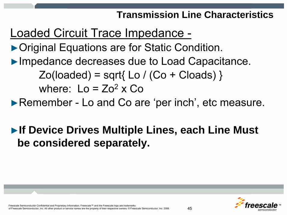
TMFreescale Semiconductor Confidential and Proprietary Information. Freescale™ and the Freescale logo are trademarksof Freescale Semiconductor, Inc. All other product or service names are the property of their respective owners. © Freescale Semiconductor, Inc. 2008. 45
Loaded Circuit Trace Impedance -►Original Equations are for Static Condition.►Impedance decreases due to Load Capacitance.
Zo(loaded) = sqrt{ Lo / (Co + Cloads) }where: Lo = Zo2 x Co
►Remember - Lo and Co are ‘per inch’, etc measure.
►If Device Drives Multiple Lines, each Line Must be considered separately.
Transmission Line Characteristics

TMFreescale Semiconductor Confidential and Proprietary Information. Freescale™ and the Freescale logo are trademarksof Freescale Semiconductor, Inc. All other product or service names are the property of their respective owners. © Freescale Semiconductor, Inc. 2008. 46
Reflection Mode Switching -Transmission Line Characteristics
►Device with Output Impedance (Rs) equal to Zo sets up a Voltage Divider Between Rs and Zo.
►Divider causes the Initial Line Voltage (Bench Volt-age) to be approximately 1/2 Vcc.

TMFreescale Semiconductor Confidential and Proprietary Information. Freescale™ and the Freescale logo are trademarksof Freescale Semiconductor, Inc. All other product or service names are the property of their respective owners. © Freescale Semiconductor, Inc. 2008. 47
Reflection Mode Switching -Transmission Line Characteristics
►With One Load, Reflection Mode Switching is NOT a Problem.
►Multiple Loads along the Line won’t Switch until Reflected Wave raises the Line Voltage.
TMFreescale Semiconductor Confidential and Proprietary Information. Freescale™ and the Freescale logo are trademarksof Freescale Semiconductor, Inc. All other product or service names are the property of their respective owners. © Freescale Semiconductor, Inc. 2008. 48
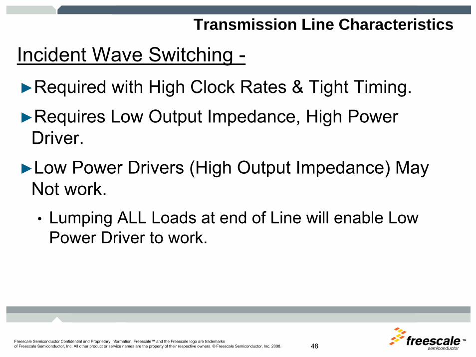
Incident Wave Switching -Transmission Line Characteristics
►Required with High Clock Rates & Tight Timing.►Requires Low Output Impedance, High Power
Driver.►Low Power Drivers (High Output Impedance) May
Not work.• Lumping ALL Loads at end of Line will enable Low
Power Driver to work.

TMFreescale Semiconductor Confidential and Proprietary Information. Freescale™ and the Freescale logo are trademarksof Freescale Semiconductor, Inc. All other product or service names are the property of their respective owners. © Freescale Semiconductor, Inc. 2008. 49
Trace Routing and Termination Style
Result of Long Stubs and No Line Termination.
Logic 1
Logic 0

TMFreescale Semiconductor Confidential and Proprietary Information. Freescale™ and the Freescale logo are trademarksof Freescale Semiconductor, Inc. All other product or service names are the property of their respective owners. © Freescale Semiconductor, Inc. 2008. 50
Trace Routing and Termination Style
Keep Stubs Shorter than 1/8 Rise Distance.
SI Partial Solution -Solid Line is original route.Dotted Line is rerouted Trace.

TMFreescale Semiconductor Confidential and Proprietary Information. Freescale™ and the Freescale logo are trademarksof Freescale Semiconductor, Inc. All other product or service names are the property of their respective owners. © Freescale Semiconductor, Inc. 2008. 51
Transmission Line Termination
►Used with Strong Drivers (Needing Incident Wave Switching).►Some Logic Families Must be Parallel Term (ECL, GTL, etc.).►Place Resistor within 1/8 Rise Distance of Last Load or just
beyond Last Load.►Resistor Value = Zo.►Resistor Needed at Both Ends of Bidirectional Net.►High Power Consumption (DC Load when Output is High).►Low Power Outputs CANNOT drive this Low Impedance.

TMFreescale Semiconductor Confidential and Proprietary Information. Freescale™ and the Freescale logo are trademarksof Freescale Semiconductor, Inc. All other product or service names are the property of their respective owners. © Freescale Semiconductor, Inc. 2008. 52
Transmission Line Termination
After Parallel Terminating Rerouted Line
p 7.000 volts
-2.000 volts
0.0 volts
0.000ns 10.000ns
1 V/div
1 nsec/div

TMFreescale Semiconductor Confidential and Proprietary Information. Freescale™ and the Freescale logo are trademarksof Freescale Semiconductor, Inc. All other product or service names are the property of their respective owners. © Freescale Semiconductor, Inc. 2008. 53
Transmission Line Termination
►Must place Resistor within 1/8 Rise Distance of Driver.►Resistor Value = Zo - Rs(Output Impedance).►Reflection occurs and is Absorbed back at the Driver.►Most common w/ Single Load or ALL Loads at end of
Line.►Low-Power Consumption.►Helps Eliminate Ground Bounce.►Lowers Power Transients and EMI Dramatically.

TMFreescale Semiconductor Confidential and Proprietary Information. Freescale™ and the Freescale logo are trademarksof Freescale Semiconductor, Inc. All other product or service names are the property of their respective owners. © Freescale Semiconductor, Inc. 2008. 54
Transmission Line Termination
After Series Terminating Rerouted Line(DO NOT Parallel AND Series Term)
Comment: Simple Series Terminated Transmission Line 8.000 volts
-1.000 volts
0.0 volts
0.000ns 20.000ns
1 V/div
2 nsec/div

TMFreescale Semiconductor Confidential and Proprietary Information. Freescale™ and the Freescale logo are trademarksof Freescale Semiconductor, Inc. All other product or service names are the property of their respective owners. © Freescale Semiconductor, Inc. 2008. 55
►Form of Parallel Termination with Two Resistors.►Useful w/Strong Drivers for Incident Wave Switching.►Each Resistor tied to Reference Voltage, usually Vcc & Gnd.►User Defined DC Bias, based on Resistor Values.►Parallel Combination of Resistors = Zo.►Requires Twice the Components of most Terminations.►Resistors Needed at Both Ends of Bidirectional Net.►Very High Power Consumption (Constant DC Load).
Transmission Line Termination
TMFreescale Semiconductor Confidential and Proprietary Information. Freescale™ and the Freescale logo are trademarksof Freescale Semiconductor, Inc. All other product or service names are the property of their respective owners. © Freescale Semiconductor, Inc. 2008. 56
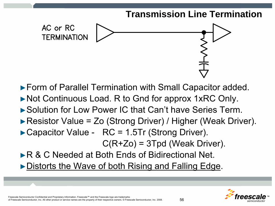
Transmission Line Termination
►Form of Parallel Termination with Small Capacitor added.►Not Continuous Load. R to Gnd for approx 1xRC Only.►Solution for Low Power IC that Can’t have Series Term.►Resistor Value = Zo (Strong Driver) / Higher (Weak Driver).►Capacitor Value - RC = 1.5Tr (Strong Driver).
C(R+Zo) = 3Tpd (Weak Driver).►R & C Needed at Both Ends of Bidirectional Net.►Distorts the Wave of both Rising and Falling Edge.

TMFreescale Semiconductor Confidential and Proprietary Information. Freescale™ and the Freescale logo are trademarksof Freescale Semiconductor, Inc. All other product or service names are the property of their respective owners. © Freescale Semiconductor, Inc. 2008. 57
Transmission Line Routing and Termination
►Termination Not Needed IF -• Output Impedance is 2/3 Zo or higher. (OR)• Line is Shorter than “Max Line Length”.
►When needed, Series Termination is Best.• Works whether Single Ended or Bi-directional.• No Reflection Mode Delays w/ Single Load.
►Parallel, RC or Thevinin Terminate IF -• Logic Family Demands (ECL, BTL, GTL, etc.).
Point-to-Point

TMFreescale Semiconductor Confidential and Proprietary Information. Freescale™ and the Freescale logo are trademarksof Freescale Semiconductor, Inc. All other product or service names are the property of their respective owners. © Freescale Semiconductor, Inc. 2008. 58
Transmission Line Routing and Termination
►Termination Not Needed IF -• Output Impedance is 2/3 Zo or higher. (OR)• Line is Shorter than “Max Line Length”.
►When needed, Series Termination is Best.• Works whether Single Ended or Bi-directional.• No Reflection Mode Delays w/ Loads at End of Line.
►Parallel, RC or Thevinin Terminate IF -• Logic Family Demands (ECL, BTL, GTL, etc.).
Tee Route

TMFreescale Semiconductor Confidential and Proprietary Information. Freescale™ and the Freescale logo are trademarksof Freescale Semiconductor, Inc. All other product or service names are the property of their respective owners. © Freescale Semiconductor, Inc. 2008. 59
Transmission Line Routing and Termination
►Termination Not Needed IF -• Line is Shorter Than “Max Line Length”. (OR)• Output Impedance is 2/3 Zo or higher. (AND)• Driver(s) at one or Both Ends of Line.
►When needed, Series Termination is Best if -• Driver(s) at One End or Both Ends of Line.• Reflection Mode Delays don’t affect Timing.
►Parallel, RC or Thevinin Terminate IF -• Logic Family Demands (ECL, BTL, GTL, etc.).• Driver in the Middle of the Line (Terminate Both Ends).
Daisy Chain

TMFreescale Semiconductor Confidential and Proprietary Information. Freescale™ and the Freescale logo are trademarksof Freescale Semiconductor, Inc. All other product or service names are the property of their respective owners. © Freescale Semiconductor, Inc. 2008. 60
Transmission Line Routing and Termination
►Used if Loads are Far Apart and -• Need to have Incident Wave Switching.• (AND/OR) Minimized Skew.
►Requires a Very Strong Driver (Driver Must be able to Source Zo / N).
Branch by ‘N’

TMFreescale Semiconductor Confidential and Proprietary Information. Freescale™ and the Freescale logo are trademarksof Freescale Semiconductor, Inc. All other product or service names are the property of their respective owners. © Freescale Semiconductor, Inc. 2008. 61
Branch by ‘N’ (Cont’d)
►Termination Not Needed IF -• Output Impedance somewhat Matches Zo / N.• (OR) Lines Shorter than “Max Line Length”.
►Series Terminate -• IF Branches are approx Equal in Length.• With One resistor equal to Zo / N minus Driver’s
Output Impedance (Logic Family Dependent) (OR)• With ‘N’ resistors (one for each branch) equal to Zo
minus Impedance of Driver.
Transmission Line Routing and Termination

TMFreescale Semiconductor Confidential and Proprietary Information. Freescale™ and the Freescale logo are trademarksof Freescale Semiconductor, Inc. All other product or service names are the property of their respective owners. © Freescale Semiconductor, Inc. 2008. 62
Signal / Wave Attenuation
1) Reflections - Due to Impedance Mismatch.(Previously Discussed)
2) Signal Cross Talk (Will Discuss).3) Power Bus (Switching) Noise (Will Discuss).4) Ground/Vcc Bounce (Ldi/dt Losses).5) Skin Effect (Resistive Loss in Conductor).6) Loss Tangent (Property of Molecular make-up
of PCB Dielectric).

TMFreescale Semiconductor Confidential and Proprietary Information. Freescale™ and the Freescale logo are trademarksof Freescale Semiconductor, Inc. All other product or service names are the property of their respective owners. © Freescale Semiconductor, Inc. 2008. 63
Signal / Wave Attenuation
= Noise Budget / Noise Margin =
VOH max
VIH minVOH min
Noise Margin

TMFreescale Semiconductor Confidential and Proprietary Information. Freescale™ and the Freescale logo are trademarksof Freescale Semiconductor, Inc. All other product or service names are the property of their respective owners. © Freescale Semiconductor, Inc. 2008. 64
Signal / Wave Attenuation
= Noise Budget / Noise Margin =

TMFreescale Semiconductor Confidential and Proprietary Information. Freescale™ and the Freescale logo are trademarksof Freescale Semiconductor, Inc. All other product or service names are the property of their respective owners. © Freescale Semiconductor, Inc. 2008. 65
Signal / Wave Attenuation - Reflections
5
60Ω
Line Impedance - 60 Ω
(57Ω-
(54Ω-66Ω)
A B
4.58V
0V
AB
Load Z - 63ΩLine Z - 54Ω
4.93V4.61V
4.61V 4.58V
63Ω)
►When Termination Value equals Ideal Line Zo, both Pos and NegReflections occur.
0V
Load Z - 57ΩLine Z - 66Ω
AB
4.65V 4.60V
4.30V

TMFreescale Semiconductor Confidential and Proprietary Information. Freescale™ and the Freescale logo are trademarksof Freescale Semiconductor, Inc. All other product or service names are the property of their respective owners. © Freescale Semiconductor, Inc. 2008. 66
Signal / Wave Attenuation - Reflections
5
68Ω
Line Impedance - 60 Ω
(65Ω-
(54Ω-66Ω)
A B
4.58V
0V
AB
Load Z - 71ΩLine Z - 54Ω
5.22V4.66V
4.68V 4.61V
71Ω)
0V
Load Z - 65ΩLine Z - 66Ω
AB
4.65V4.64V
4.61V
►Select Termination that Always causes reasonable Positive Reflec-tions and Tiny Negative Reflections.

TMFreescale Semiconductor Confidential and Proprietary Information. Freescale™ and the Freescale logo are trademarksof Freescale Semiconductor, Inc. All other product or service names are the property of their respective owners. © Freescale Semiconductor, Inc. 2008. 67
Signal / Wave Attenuation - Reflections
5
80Ω
Line Impedance - 60 Ω
(64Ω-
(54Ω-66Ω)
4.57V
0V
A B
AB
Load Z - 96ΩLine Z - 54Ω
96Ω)
5.85V
4.82V
4.80V 4.50V
0V
Load Z - 64ΩLine Z - 66Ω
AB
4.64V4.64V
4.58V
►When ‘R’ is EP (+/-20%) apply same principal for small neg Reflections.
4.75V
TMFreescale Semiconductor Confidential and Proprietary Information. Freescale™ and the Freescale logo are trademarksof Freescale Semiconductor, Inc. All other product or service names are the property of their respective owners. © Freescale Semiconductor, Inc. 2008. 68
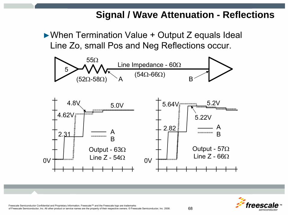
Signal / Wave Attenuation - Reflections
555Ω
Line Impedance - 60Ω
(52Ω-58Ω) A B
►When Termination Value + Output Z equals Ideal Line Zo, small Pos and Neg Reflections occur.
0V 0V
2.31
4.62V
BA B
A2.82
4.8V 5.0V
5.22V
5.64V 5.2V
Output - 63ΩLine Z - 54Ω
Output - 57ΩLine Z - 66Ω
(54Ω-66Ω)
TMFreescale Semiconductor Confidential and Proprietary Information. Freescale™ and the Freescale logo are trademarksof Freescale Semiconductor, Inc. All other product or service names are the property of their respective owners. © Freescale Semiconductor, Inc. 2008. 69
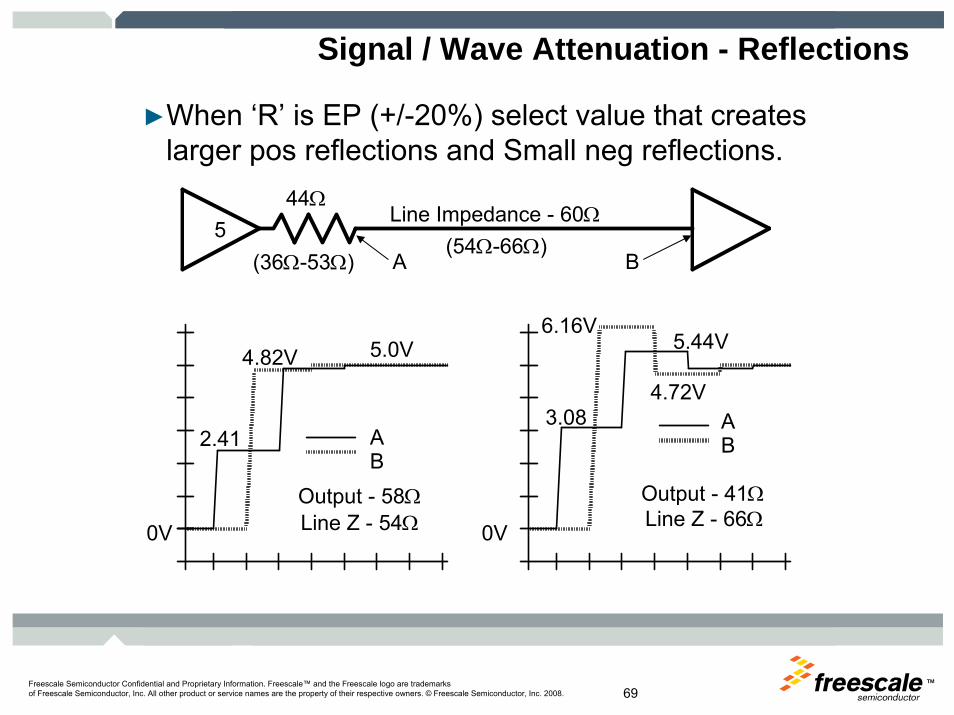
Signal / Wave Attenuation - Reflections
544Ω
Line Impedance - 60Ω
(36Ω-53Ω) A B
►When ‘R’ is EP (+/-20%) select value that creates larger pos reflections and Small neg reflections.
0V 0V
2.41BA B
A3.08
4.82V 5.0V
4.72V
6.16V5.44V
Output - 58ΩLine Z - 54Ω
Output - 41ΩLine Z - 66Ω
(54Ω-66Ω)

TMFreescale Semiconductor Confidential and Proprietary Information. Freescale™ and the Freescale logo are trademarksof Freescale Semiconductor, Inc. All other product or service names are the property of their respective owners. © Freescale Semiconductor, Inc. 2008. 70
Signal / Wave Attenuation
Ground or Vcc Bounce-►Results when Very Fast Switching Currents cause
a Voltage Drop across the Power or Ground pins of an IC.
V = Ldi/dtWhere: L = Inductance of IC Pin(s)
di = Current Needed to Charge or Discharge Transmission Lines.
dt = Rise Time or Fall Time of IC.

TMFreescale Semiconductor Confidential and Proprietary Information. Freescale™ and the Freescale logo are trademarksof Freescale Semiconductor, Inc. All other product or service names are the property of their respective owners. © Freescale Semiconductor, Inc. 2008. 71
Signal / Wave Attenuation
Ground or Vcc Bounce-►The large Voltage Drop causes Power in the IC to
Fall Below a Minimum Acceptable Level or for 0v (Ground) in the IC to Raise Above a Maximum Acceptable Level.
►Remedies -• Low Inductance Lead Frame ICs.• Multiple Power and Ground Pins in IC Lead Frame.• Very Short Power and Ground Paths• Proper Location of Power / Ground Vias.• All of the Above.

TMFreescale Semiconductor Confidential and Proprietary Information. Freescale™ and the Freescale logo are trademarksof Freescale Semiconductor, Inc. All other product or service names are the property of their respective owners. © Freescale Semiconductor, Inc. 2008. 72
Signal / Wave AttenuationSample Vcc Bounce Calculation -
1) 50ma drive current / Memory Line X 32 lines = 1.6 Amps.2) 30 Power Pins (Memory) @ 12nH per pin = .4 nH total.3) Z of pins = 2πFL = 6.28 x 100MHz x .4nH = .251 ohm.4) .251 (Pin Z) x 1.6 Amps (item 1) = .40V drop across pins.5) 3.3V (Vcc) - .40V (item 4) = 2.90V, minus 200mV internal
V drop within 8245 IC = 2.7V(Vcc) left to drive Memory.6) 2.7V (item 5) into 6 ohm (min 8245 output Z) to 50 ohm
(Trace Zo) Voltage Divider = 2.39V Incident Wave.7) Vin High Min for 8245 PowerPC is 2.0 V, leaving Noise
Margin = 390 mv.
What if Crosstalk, Power Bus Noise & Reflections add up to more than 390 mv??????

TMFreescale Semiconductor Confidential and Proprietary Information. Freescale™ and the Freescale logo are trademarksof Freescale Semiconductor, Inc. All other product or service names are the property of their respective owners. © Freescale Semiconductor, Inc. 2008. 73
Attenuation- PCB Trace Corners
Which of these is BEST?

TMFreescale Semiconductor Confidential and Proprietary Information. Freescale™ and the Freescale logo are trademarksof Freescale Semiconductor, Inc. All other product or service names are the property of their respective owners. © Freescale Semiconductor, Inc. 2008. 74
Signal / Wave Attenuation- Reflection Amplitude vs Rise Time -►Per given Length of Discontinuity, Amplitude of a
Reflection is a Function of Rise Time.
(Info from Speeding Edge, Spring 2001)

TMFreescale Semiconductor Confidential and Proprietary Information. Freescale™ and the Freescale logo are trademarksof Freescale Semiconductor, Inc. All other product or service names are the property of their respective owners. © Freescale Semiconductor, Inc. 2008. 75
Signal / Wave Attenuation- Reflection vs Discontinuity Length -
►Said Another Way- Per given Rise Time (i.e.- 1.0ns), Amp-litude of a Reflection is a Function of Discontinuity Length.
►From the % Reflection Equation, 2 Reflections occur, One Positive and One Negative.

TMFreescale Semiconductor Confidential and Proprietary Information. Freescale™ and the Freescale logo are trademarksof Freescale Semiconductor, Inc. All other product or service names are the property of their respective owners. © Freescale Semiconductor, Inc. 2008. 76
Signal / Wave Attenuation- Reflection vs Discontinuity Length -
►If ‘L’ is At or Beyond 1/4 of Rise Distance, Reflections reach Maximum Size.
►Reflections from 1.0 ns Signal, w/ ‘L’ at 4.0”.
►Signal at first 50 ohm Segment and middle of Discontinuity.
TMFreescale Semiconductor Confidential and Proprietary Information. Freescale™ and the Freescale logo are trademarksof Freescale Semiconductor, Inc. All other product or service names are the property of their respective owners. © Freescale Semiconductor, Inc. 2008. 77
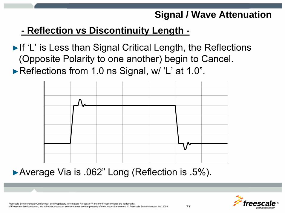
Signal / Wave Attenuation- Reflection vs Discontinuity Length -
►If ‘L’ is Less than Signal Critical Length, the Reflections (Opposite Polarity to one another) begin to Cancel.
►Reflections from 1.0 ns Signal, w/ ‘L’ at 1.0”.
►Average Via is .062” Long (Reflection is .5%).

TMFreescale Semiconductor Confidential and Proprietary Information. Freescale™ and the Freescale logo are trademarksof Freescale Semiconductor, Inc. All other product or service names are the property of their respective owners. © Freescale Semiconductor, Inc. 2008. 78
Signal / Wave Attenuation- Conventional Connectors -
►Connector Assignments should be:
- Best
- OK

TMFreescale Semiconductor Confidential and Proprietary Information. Freescale™ and the Freescale logo are trademarksof Freescale Semiconductor, Inc. All other product or service names are the property of their respective owners. © Freescale Semiconductor, Inc. 2008. 79
Cross Talk
►Transfer of Pulse Energy from an Active Source Line to a Passive Victim Line.
►Coupled Capacitively, Inductively or Both.
►Cross Talk occurs when Signal Traces route in Parallel for an extended distance, Side-by-Side or on Adjacent Layers.• Adjacent layer parallelism is Much Worse.
►Increases, per given Trace Length, as Tr Increases.
TMFreescale Semiconductor Confidential and Proprietary Information. Freescale™ and the Freescale logo are trademarksof Freescale Semiconductor, Inc. All other product or service names are the property of their respective owners. © Freescale Semiconductor, Inc. 2008. 80
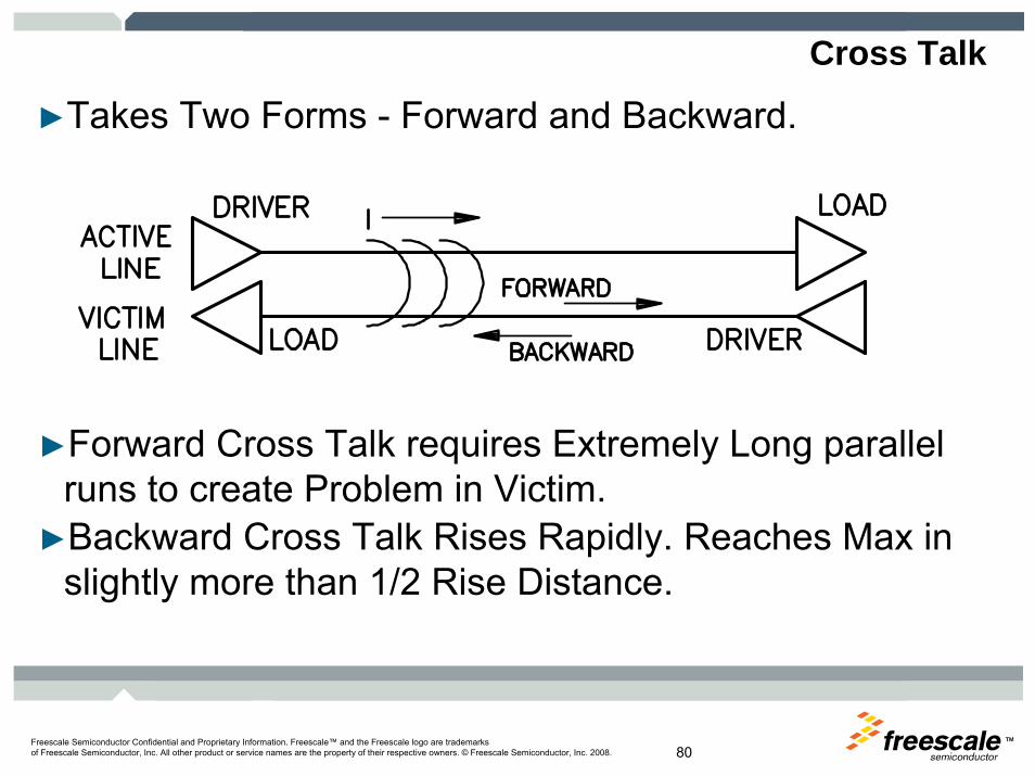
Cross Talk
►Takes Two Forms - Forward and Backward.
►Forward Cross Talk requires Extremely Long parallel runs to create Problem in Victim.
►Backward Cross Talk Rises Rapidly. Reaches Max in slightly more than 1/2 Rise Distance.

TMFreescale Semiconductor Confidential and Proprietary Information. Freescale™ and the Freescale logo are trademarksof Freescale Semiconductor, Inc. All other product or service names are the property of their respective owners. © Freescale Semiconductor, Inc. 2008. 81
Cross Talk
►Forward Cross Talk -• Coupled Pulse Width equals Tr of the Signal of the
Coupling Line.• Takes Parallel Runs of 4 to 6 Times Rise Distance to
Couple enough Energy to cause a Problem.• Coupled Pulse Amplitude grows until it’s equal to
Amplitude of Signal from Coupling Line.• Coupled Pulse is the Opposite Polarity as Signal from
the Aggressor Line.

TMFreescale Semiconductor Confidential and Proprietary Information. Freescale™ and the Freescale logo are trademarksof Freescale Semiconductor, Inc. All other product or service names are the property of their respective owners. © Freescale Semiconductor, Inc. 2008. 82
Cross Talk
►Backward Cross Talk -• Coupled Pulse Width equals 2 x Propagation Time of
Parallelism.• Coupled Pulse Amplitude rises until Parallelism
equals ‘Cross Talk Critical Length’.• Then, Coupled Pulse Levels off and gets Wider.• Amount of Coupling in ‘Xtalk Critical Length’ is a func-
tion of Separation vs Height above Plane.• Coupled Pulse is the Same Polarity as the Signal from
the Aggressor Line.

TMFreescale Semiconductor Confidential and Proprietary Information. Freescale™ and the Freescale logo are trademarksof Freescale Semiconductor, Inc. All other product or service names are the property of their respective owners. © Freescale Semiconductor, Inc. 2008. 83
Cross Talk
►Backward Cross Talk Critical Length -
Er = 2
Er = 3
Er = 4
TMFreescale Semiconductor Confidential and Proprietary Information. Freescale™ and the Freescale logo are trademarksof Freescale Semiconductor, Inc. All other product or service names are the property of their respective owners. © Freescale Semiconductor, Inc. 2008. 84
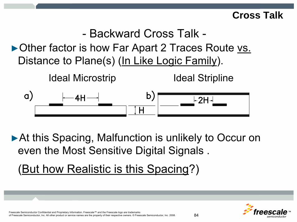
Cross Talk
- Backward Cross Talk -►Other factor is how Far Apart 2 Traces Route vs.
Distance to Plane(s) (In Like Logic Family).Ideal Microstrip Ideal Stripline
►At this Spacing, Malfunction is unlikely to Occur on even the Most Sensitive Digital Signals .
(But how Realistic is this Spacing?)

TMFreescale Semiconductor Confidential and Proprietary Information. Freescale™ and the Freescale logo are trademarksof Freescale Semiconductor, Inc. All other product or service names are the property of their respective owners. © Freescale Semiconductor, Inc. 2008. 85
Cross Talk
- Backward Cross Talk -►In the Real World, 4H and 2H Separations are Highly
Unlikely, in all but a Few Situations.Realistic Microstrip Realistic Stripline
►Amount of Coupling (Approx 10%) Generally will Not be enough to cause Malfunction.
(Within Like Logic Families!!!)

TMFreescale Semiconductor Confidential and Proprietary Information. Freescale™ and the Freescale logo are trademarksof Freescale Semiconductor, Inc. All other product or service names are the property of their respective owners. © Freescale Semiconductor, Inc. 2008. 86
Cross Talk- Backward Cross Talk -

TMFreescale Semiconductor Confidential and Proprietary Information. Freescale™ and the Freescale logo are trademarksof Freescale Semiconductor, Inc. All other product or service names are the property of their respective owners. © Freescale Semiconductor, Inc. 2008. 87
Cross Talk- Backward Cross Talk -

TMFreescale Semiconductor Confidential and Proprietary Information. Freescale™ and the Freescale logo are trademarksof Freescale Semiconductor, Inc. All other product or service names are the property of their respective owners. © Freescale Semiconductor, Inc. 2008. 88
Cross Talk
- Guard Traces -►On Single or Double Sided PC Board:
• Critical Routes- Self and Loop Inductance are Dramatically Improved.
• Guard Trace to Route Parallel to Critical Trace, Same Layer.
• Connect to Ground at Driver and Receiver.• Ground at ONE End Only is Electrostatic Shield ONLY.
►No Real Benefit On Properly Structured Multi-layer Digital PC Board.

TMFreescale Semiconductor Confidential and Proprietary Information. Freescale™ and the Freescale logo are trademarksof Freescale Semiconductor, Inc. All other product or service names are the property of their respective owners. © Freescale Semiconductor, Inc. 2008. 89
Cross Talk- Guard Traces -Bandpass Filter made from Strips of Copper.
Side by side traces, such as “Guard Traces” can inadvertently enhance coupling by creating a band pass filter. Traces, no matter how their ends are connected to underlying planes, are LC networks that resonate at some frequency.
TMFreescale Semiconductor Confidential and Proprietary Information. Freescale™ and the Freescale logo are trademarksof Freescale Semiconductor, Inc. All other product or service names are the property of their respective owners. © Freescale Semiconductor, Inc. 2008. 90
Electro-Magnetic Interference (EMI)
►EMI is that condition where a Circuit or System has sufficient Radiated or Conducted Energy to interfere with performance of other Circuits or Systems.
►EMI is the Transfer or Coupling of Pulse Energy from an active Circuit or Signal Source to a less active Victim Circuit.

TMFreescale Semiconductor Confidential and Proprietary Information. Freescale™ and the Freescale logo are trademarksof Freescale Semiconductor, Inc. All other product or service names are the property of their respective owners. © Freescale Semiconductor, Inc. 2008. 91
Control of Electro-Magnetic Interference (EMI)
►All Circuits have CM Noise caused by Voltage Drops across inductance in circuit elements and Stray Magnetic Fields in Finite Current Loops -• In Power / Ground Bus.• Across Circuit Traces• In IC Pins & Interposer Boards in IC Pkg.• Across Connector Pins• etc.

TMFreescale Semiconductor Confidential and Proprietary Information. Freescale™ and the Freescale logo are trademarksof Freescale Semiconductor, Inc. All other product or service names are the property of their respective owners. © Freescale Semiconductor, Inc. 2008. 92
Types of Electro-Magnetic Interference (EMI)
►Electro-Magnetic Energy can exist in Two forms:• Differential Mode.• Common Mode.
►The Difference becomes easier to understand when thinking in terms of Current Flow, instead of Voltage.

TMFreescale Semiconductor Confidential and Proprietary Information. Freescale™ and the Freescale logo are trademarksof Freescale Semiconductor, Inc. All other product or service names are the property of their respective owners. © Freescale Semiconductor, Inc. 2008. 93
Types of Electro-Magnetic Interference (EMI)
- EMI- Differential Mode -
►An IC sends a Current down a trace, an Equal Cur-rent is returned to driver / All received at Load.
►These Equal Currents, traveling in Opposite Directions, are Differential Mode Operation.
►Since a PCB only emulates a Coax, complete E-field and H-field containment is Not possible.
►Radiating Stray fields are Differential Mode EMI.
TMFreescale Semiconductor Confidential and Proprietary Information. Freescale™ and the Freescale logo are trademarksof Freescale Semiconductor, Inc. All other product or service names are the property of their respective owners. © Freescale Semiconductor, Inc. 2008. 94
Types of Electro-Magnetic Interference (EMI)
- EMI- Common Mode -
►Caused by Common Mode Current-
►CM is Unwanted Current, flowing in Common Direction, through Unintended Paths.• Signal Not Paired Directly with an Equal and Opposite
Current.• Voltage Transients Generated on Power / Ground
Planes (V = Ldi/dt).
►CM Noise is usually Common to Several Conductors.
TMFreescale Semiconductor Confidential and Proprietary Information. Freescale™ and the Freescale logo are trademarksof Freescale Semiconductor, Inc. All other product or service names are the property of their respective owners. © Freescale Semiconductor, Inc. 2008. 95
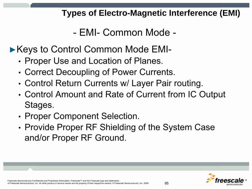
Types of Electro-Magnetic Interference (EMI)
- EMI- Common Mode -
►Keys to Control Common Mode EMI-• Proper Use and Location of Planes.• Correct Decoupling of Power Currents.• Control Return Currents w/ Layer Pair routing.• Control Amount and Rate of Current from IC Output
Stages.• Proper Component Selection.• Provide Proper RF Shielding of the System Case
and/or Proper RF Ground.

TMFreescale Semiconductor Confidential and Proprietary Information. Freescale™ and the Freescale logo are trademarksof Freescale Semiconductor, Inc. All other product or service names are the property of their respective owners. © Freescale Semiconductor, Inc. 2008. 96
Power Distribution System
►Design feature of PC Board with enormous impact on output Signal Integrity & EMI.
►The Foundation of the ‘Building’.►If Power System fails to provide Current to Output
Stages at any Frequency in spectrum-• Transients Develop and EMI risk severely increases.• IC Rising / Falling Edges can be distorted, creating
Non-Monotonic Signals.

TMFreescale Semiconductor Confidential and Proprietary Information. Freescale™ and the Freescale logo are trademarksof Freescale Semiconductor, Inc. All other product or service names are the property of their respective owners. © Freescale Semiconductor, Inc. 2008. 97
Power Distribution System
►If Output Tr is 1.0 ns, Power System Must Deliver Energy to Output Stage of IC in 1.0 ns.
►Power to Drive IC Output Cannot come from Power Supply directly, due to Inductance.
►Frequency of Power is from ‘Clock’ to ‘.50/Tr’.
TMFreescale Semiconductor Confidential and Proprietary Information. Freescale™ and the Freescale logo are trademarksof Freescale Semiconductor, Inc. All other product or service names are the property of their respective owners. © Freescale Semiconductor, Inc. 2008. 98
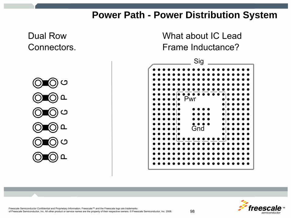
Power Path - Power Distribution System
Dual Row What about IC LeadConnectors. Frame Inductance?
Sig
Gnd
Pwr
TMFreescale Semiconductor Confidential and Proprietary Information. Freescale™ and the Freescale logo are trademarksof Freescale Semiconductor, Inc. All other product or service names are the property of their respective owners. © Freescale Semiconductor, Inc. 2008. 99
Decoupling - Power Distribution System
►Due to Inertia, Power Supply can’t respond Rapidly to Demands for Current to ICs.
►Power System Capacitance (High Frequency Tank of Energy) Provides High Speed Current until Power Supply can respond.
►Multiple Harmonics Require -• Power Bus Capacitance be high at broad range of
Frequencies.• Power Bus Inductance MUST be Low.• Power Bus Impedance MUST be VERY Low.

TMFreescale Semiconductor Confidential and Proprietary Information. Freescale™ and the Freescale logo are trademarksof Freescale Semiconductor, Inc. All other product or service names are the property of their respective owners. © Freescale Semiconductor, Inc. 2008. 100
Decoupling - Power Distribution System
Usual Connections for Decoupling-►One Cap per Pair of Power & Ground Pins???►Large Vias???
►If Cap to IC distance greater than .125”, Via Cap and IC directly to Planes.
►Which is Best? Is either Ideal or Necessary?

TMFreescale Semiconductor Confidential and Proprietary Information. Freescale™ and the Freescale logo are trademarksof Freescale Semiconductor, Inc. All other product or service names are the property of their respective owners. © Freescale Semiconductor, Inc. 2008. 101
Decoupling - Power Distribution System
►Capacitor’s ability to provide Energy is a function of Caps Reactance (Z) vs. Frequency -
Capacitor’s Impedance vs. Frequency.
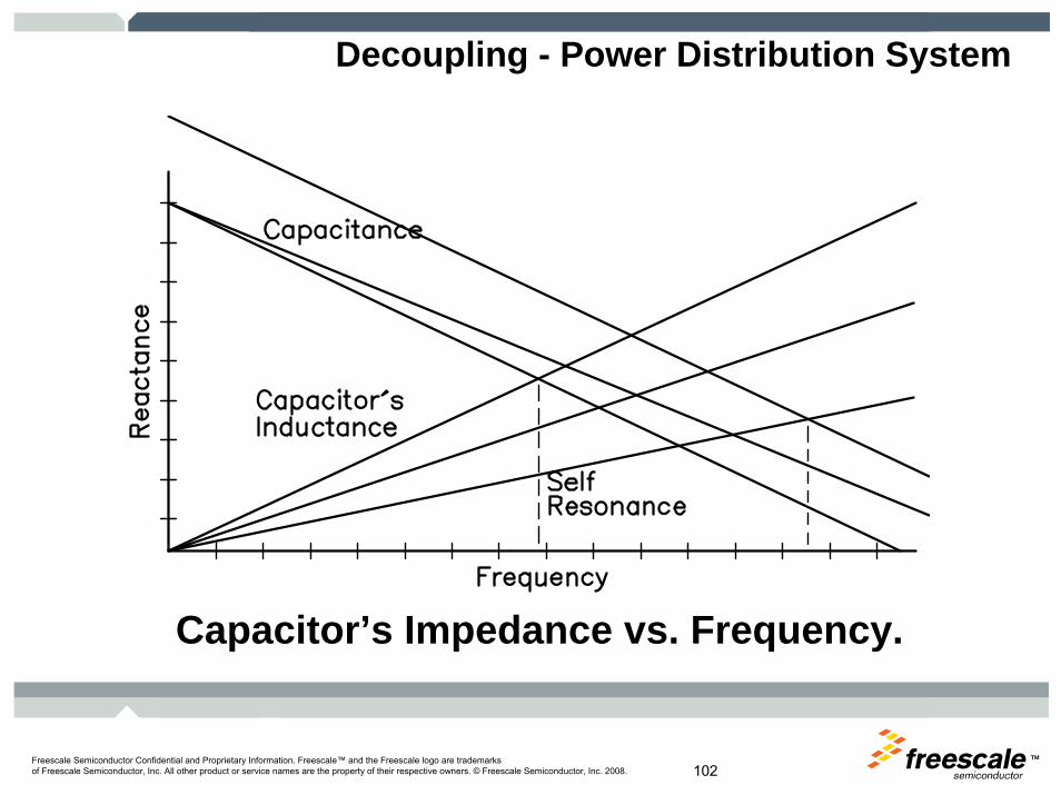
TMFreescale Semiconductor Confidential and Proprietary Information. Freescale™ and the Freescale logo are trademarksof Freescale Semiconductor, Inc. All other product or service names are the property of their respective owners. © Freescale Semiconductor, Inc. 2008. 102
Decoupling - Power Distribution System
Capacitor’s Impedance vs. Frequency.

TMFreescale Semiconductor Confidential and Proprietary Information. Freescale™ and the Freescale logo are trademarksof Freescale Semiconductor, Inc. All other product or service names are the property of their respective owners. © Freescale Semiconductor, Inc. 2008. 103
Decoupling - Power Distribution System
Cap Lead Frame Inductance (Per AVX):Axial Lead - 2000 pH1206 SMD - 1250 pH0805 SMD - 1050 pH1210 SMD - 980 pH0603 SMD - 870 pH0402 SMD - 650 pH Side Mounted Leads
0612 SMD - 610 pH0508 SMD - 600 pH16 pin BGA- 50 pH

TMFreescale Semiconductor Confidential and Proprietary Information. Freescale™ and the Freescale logo are trademarksof Freescale Semiconductor, Inc. All other product or service names are the property of their respective owners. © Freescale Semiconductor, Inc. 2008. 104
Decoupling - Power Distribution System
Intended Goal of Two Parallel Capacitors.
Z
Frequency
1000pF
0.1uF
TMFreescale Semiconductor Confidential and Proprietary Information. Freescale™ and the Freescale logo are trademarksof Freescale Semiconductor, Inc. All other product or service names are the property of their respective owners. © Freescale Semiconductor, Inc. 2008. 105
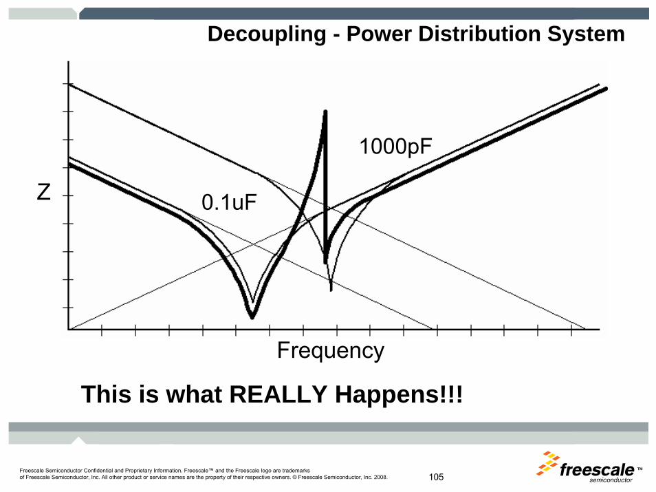
Decoupling - Power Distribution System
This is what REALLY Happens!!!
Z
Frequency
1000pF
0.1uF

TMFreescale Semiconductor Confidential and Proprietary Information. Freescale™ and the Freescale logo are trademarksof Freescale Semiconductor, Inc. All other product or service names are the property of their respective owners. © Freescale Semiconductor, Inc. 2008. 106
Decoupling - Power Distribution System
Planes alone Often don’t have adequate Capacity.
TMFreescale Semiconductor Confidential and Proprietary Information. Freescale™ and the Freescale logo are trademarksof Freescale Semiconductor, Inc. All other product or service names are the property of their respective owners. © Freescale Semiconductor, Inc. 2008. 107
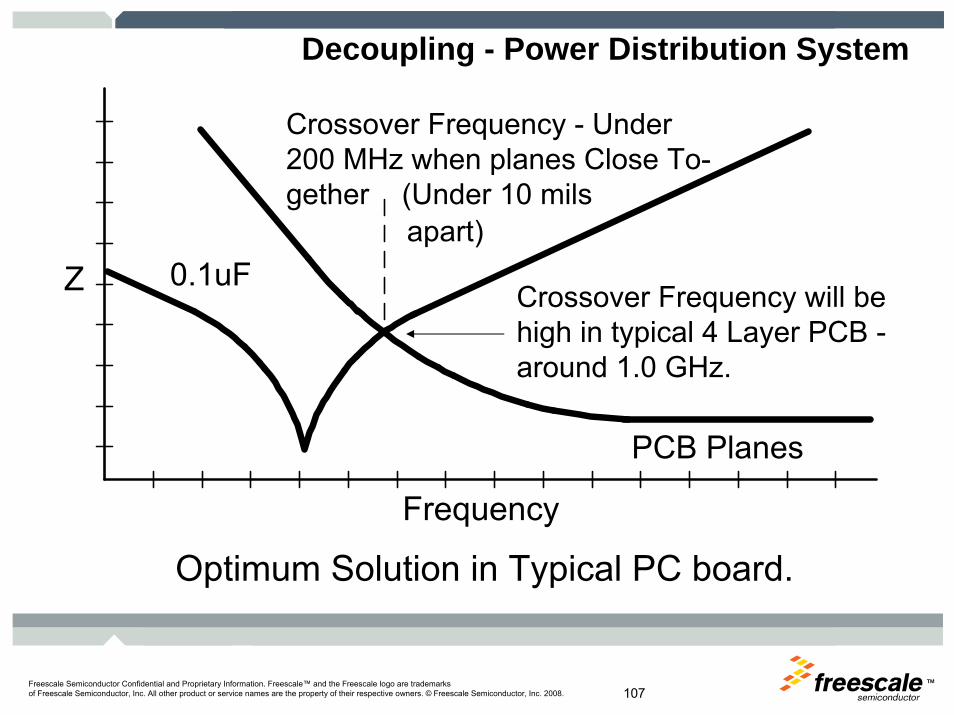
Decoupling - Power Distribution System
Optimum Solution in Typical PC board.
Z
Frequency
Crossover Frequency - Under 200 MHz when planes Close To-gether (Under 10 mils
apart)0.1uF
PCB Planes
Crossover Frequency will be high in typical 4 Layer PCB -around 1.0 GHz.

TMFreescale Semiconductor Confidential and Proprietary Information. Freescale™ and the Freescale logo are trademarksof Freescale Semiconductor, Inc. All other product or service names are the property of their respective owners. © Freescale Semiconductor, Inc. 2008. 108
Decoupling - Power Distribution SystemTI’s ‘Opinion’ on Decoupling
►Think about the importance of connecting the planes to the IC through a Low Inductance path, then ponder whether TI’s Strategy is better???
TI’s App Note is correct for 2 Layer & conventional 4 layer Boards.
Many research papers explain why ‘NOT’ to use the bottom structure on 6 layers and up.

TMFreescale Semiconductor Confidential and Proprietary Information. Freescale™ and the Freescale logo are trademarksof Freescale Semiconductor, Inc. All other product or service names are the property of their respective owners. © Freescale Semiconductor, Inc. 2008. 109
Decoupling - Power Distribution System
Power and Ground Planes.003” to .006” Spacing creates a Large
Plate Capacitor of Very Low Inductance.
- Don’t try this on 4 Layer Boards -

TMFreescale Semiconductor Confidential and Proprietary Information. Freescale™ and the Freescale logo are trademarksof Freescale Semiconductor, Inc. All other product or service names are the property of their respective owners. © Freescale Semiconductor, Inc. 2008. 110
Decoupling - Power Distribution System
Most PC Boards are “Foil Laminated”
Copper Foil
Copper Foil
25 to 45 Mil Thick‘C’ Stage Core
‘C’ Stage Core
‘C’ Stage Core

TMFreescale Semiconductor Confidential and Proprietary Information. Freescale™ and the Freescale logo are trademarksof Freescale Semiconductor, Inc. All other product or service names are the property of their respective owners. © Freescale Semiconductor, Inc. 2008. 111
Decoupling - Power Distribution System
►Power Bus Switching Noise relative to spacing between Power and Ground.
(Source: University of Missouri at Rolla)

TMFreescale Semiconductor Confidential and Proprietary Information. Freescale™ and the Freescale logo are trademarksof Freescale Semiconductor, Inc. All other product or service names are the property of their respective owners. © Freescale Semiconductor, Inc. 2008. 112
Decoupling - Power Distribution System
- Multistage, Multipin Capacitors -
GroundPower
GroundPowerPower
GroundPower
Ground
1206 x 4 - 70 pH* 0603 - 50 pH*
X2Y CapArray
(* when connected per manufacturer’s recommended via structure)
TMFreescale Semiconductor Confidential and Proprietary Information. Freescale™ and the Freescale logo are trademarksof Freescale Semiconductor, Inc. All other product or service names are the property of their respective owners. © Freescale Semiconductor, Inc. 2008. 113
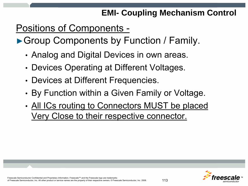
EMI- Coupling Mechanism Control
Positions of Components -►Group Components by Function / Family.
• Analog and Digital Devices in own areas.• Devices Operating at Different Voltages.• Devices at Different Frequencies.• By Function within a Given Family or Voltage.• All ICs routing to Connectors MUST be placed
Very Close to their respective connector.

TMFreescale Semiconductor Confidential and Proprietary Information. Freescale™ and the Freescale logo are trademarksof Freescale Semiconductor, Inc. All other product or service names are the property of their respective owners. © Freescale Semiconductor, Inc. 2008. 114
EMI- Coupling Mechanism Control
Approximate order of Parts Placement1) Parts Fixed by mechanical design.
• Mounting Holes.• I/O connectors.• ICs mounted to Heat Sinks that Attach to unit
Chassis.• Any other Semi-Fixed components.
Exact position of these MUST be Negotiable (can be tweaked slightly to accommodate components on very dense designs).

TMFreescale Semiconductor Confidential and Proprietary Information. Freescale™ and the Freescale logo are trademarksof Freescale Semiconductor, Inc. All other product or service names are the property of their respective owners. © Freescale Semiconductor, Inc. 2008. 115
EMI- Coupling Mechanism Control
Items Fixed by the Mechanical Design
1 1 11- IC with Heat Sink to Case.
1- Analog I/O Conns.
1- Conn to another PCB.
1- Digital I/O Conns.
1- Power Conn.1- Conn to Front Switches.
11
1

TMFreescale Semiconductor Confidential and Proprietary Information. Freescale™ and the Freescale logo are trademarksof Freescale Semiconductor, Inc. All other product or service names are the property of their respective owners. © Freescale Semiconductor, Inc. 2008. 116
EMI- Coupling Mechanism Control
Approximate order of Parts Placement2) Parts in Main I/O sections (EMI concern) -
• I/O Parts Grouped AT the I/O connectors.• Analog Section(s) get Priority.
3) Components with inputs or outputs that route off the board, through a power cable, signal cable within unit, cable to front panel switches, etc. (EMI Concern) -• I/O Parts Grouped AT or VERY Near the ‘Off
Board’ connector.

TMFreescale Semiconductor Confidential and Proprietary Information. Freescale™ and the Freescale logo are trademarksof Freescale Semiconductor, Inc. All other product or service names are the property of their respective owners. © Freescale Semiconductor, Inc. 2008. 117
EMI- Coupling Mechanism Control
Components Routing to the I/O
2b- Main I/O Circuit.
2a- High Freq Analog. 3- Power
Input Circuit.
3- Switch Interface Circuit.

TMFreescale Semiconductor Confidential and Proprietary Information. Freescale™ and the Freescale logo are trademarksof Freescale Semiconductor, Inc. All other product or service names are the property of their respective owners. © Freescale Semiconductor, Inc. 2008. 118
EMI- Coupling Mechanism Control
Approximate order of Parts Placement4) Components with inputs or outputs that route off
Board, through Board-to-Board Connectors. (EMI / Signal Integrity Concern)-• I/O Parts Grouped AT or Very Near the ‘Off
Board’ connector5) High Frequency Analog (in its own section).6) Low Frequency Analog (in its own section).
• Be aware of Ground currents at Low Freq.(5 or 6 become #2 if they go to I/O Connector)

TMFreescale Semiconductor Confidential and Proprietary Information. Freescale™ and the Freescale logo are trademarksof Freescale Semiconductor, Inc. All other product or service names are the property of their respective owners. © Freescale Semiconductor, Inc. 2008. 119
EMI- Coupling Mechanism Control
Board-to-Board and Analog Ckts
4- PCB Inter-face Circuit.
High Freq Analog2 instead of 5
6- Low Freq Analog.

TMFreescale Semiconductor Confidential and Proprietary Information. Freescale™ and the Freescale logo are trademarksof Freescale Semiconductor, Inc. All other product or service names are the property of their respective owners. © Freescale Semiconductor, Inc. 2008. 120
EMI- Coupling Mechanism Control
Approximate order of Parts Placement7) Analog to Digital Interface -
• A/D(s) and D/A(s) AT the Ana/Dig Junction.8) Digital section(s).
• Highest Speed Areas and Nets first.• 5V, 3.3V, etc components in Own Areas.
*Sections MUST be placed so routes from section to section do not cross through sections to which they DO NOT belong.

TMFreescale Semiconductor Confidential and Proprietary Information. Freescale™ and the Freescale logo are trademarksof Freescale Semiconductor, Inc. All other product or service names are the property of their respective owners. © Freescale Semiconductor, Inc. 2008. 121
EMI- Coupling Mechanism Control
A/Ds or D/As and Digital Sections
7- D/A Converter.
8- Digital.
* Sections must not route thru one another.
8- Digital.
8- Digital. 8- Digital.

TMFreescale Semiconductor Confidential and Proprietary Information. Freescale™ and the Freescale logo are trademarksof Freescale Semiconductor, Inc. All other product or service names are the property of their respective owners. © Freescale Semiconductor, Inc. 2008. 122
EMI- Coupling Mechanism Control
Position of Planes -►Once Parts are in Own Geographic Areas:
• Structure Power/Gnd Planes under each area.• Based on Supply Voltage for that section.• Align Gnd Plane for each Voltage to Match Shape
of Power Plane. (IF Gnd Plane to be Split)
►Analog & Digital Ground Planes Connect at Point (or Points) in Common.(ie- A/D or D/A Converter)

TMFreescale Semiconductor Confidential and Proprietary Information. Freescale™ and the Freescale logo are trademarksof Freescale Semiconductor, Inc. All other product or service names are the property of their respective owners. © Freescale Semiconductor, Inc. 2008. 123
EMI- Coupling Mechanism Control
Signal Route Positions -►Once Board is divided Geographically:
• Only Signals Common to Both Areas Route between the Areas.
• Those Signals Cross Only at Point(s) of Common Ground.
• All other Signals Must remain in Own Geographic Area and NOT cross Gaps in Planes.

TMFreescale Semiconductor Confidential and Proprietary Information. Freescale™ and the Freescale logo are trademarksof Freescale Semiconductor, Inc. All other product or service names are the property of their respective owners. © Freescale Semiconductor, Inc. 2008. 124
EMI- Coupling Mechanism Control
Ground Plane Split -►Do we NEED or WANT to Split Ground Plane in
a Circuit (A/D, 3v/5v, etc.)?
►Decision is Primarily a Function of-• Frequency.• Position of Circuit Components.• Position of Signal Routes.

TMFreescale Semiconductor Confidential and Proprietary Information. Freescale™ and the Freescale logo are trademarksof Freescale Semiconductor, Inc. All other product or service names are the property of their respective owners. © Freescale Semiconductor, Inc. 2008. 125
EMI- Coupling Mechanism Control
Ground Plane Split may be Necessary if -►Once Analog and Digital Sections are TOO
close to one another, AND -►The analog section has extreme sensitivity
• ie - -100+ dBm (1 - 2 microvolts), AND -►Fast digital signals are routed close to and in
Parallel with analog to digital interface.
►This only happens with 18+ bit A/D (or DAC) or in TX / RX circuits like cell phones.

TMFreescale Semiconductor Confidential and Proprietary Information. Freescale™ and the Freescale logo are trademarksof Freescale Semiconductor, Inc. All other product or service names are the property of their respective owners. © Freescale Semiconductor, Inc. 2008. 126
EMI- Coupling Mechanism Control
Current spread in ground plane -
Source - Dr. Bruce Archambeault - IBM
______________________________________

TMFreescale Semiconductor Confidential and Proprietary Information. Freescale™ and the Freescale logo are trademarksof Freescale Semiconductor, Inc. All other product or service names are the property of their respective owners. © Freescale Semiconductor, Inc. 2008. 127
EMI- Coupling Mechanism Control
Position of Planes -
Correct Power and Ground PlaneAlignment (When Splitting Gnd)

TMFreescale Semiconductor Confidential and Proprietary Information. Freescale™ and the Freescale logo are trademarksof Freescale Semiconductor, Inc. All other product or service names are the property of their respective owners. © Freescale Semiconductor, Inc. 2008. 128
EMI- Coupling Mechanism Control
Islands in Planes -►Recommendation of IC companies-
• If Noise Coupling to Sensitive IC(s) thru Power Plane is potential problem, segment Planes (make Island) under that IC.
►Connect Main Power/Gnd to Island -• Through Single Point, located away from Noisy
Sections of Main Planes (or)• Through Ferrite(s) or Low Value Resistor(s) or Low
Pass Filter(s).
►Should we Isolate Ground as well?

TMFreescale Semiconductor Confidential and Proprietary Information. Freescale™ and the Freescale logo are trademarksof Freescale Semiconductor, Inc. All other product or service names are the property of their respective owners. © Freescale Semiconductor, Inc. 2008. 129
EMI- Coupling Mechanism Control
Additional Routing Details -►When moving signals between layers, route on either side of
the same plane, as much as possible!!!
►When moving signals between 2 different planes, use a transfer via VERY near the signal via.
ReturnSignal
Ground
SignalReturn
Ground
Ground

TMFreescale Semiconductor Confidential and Proprietary Information. Freescale™ and the Freescale logo are trademarksof Freescale Semiconductor, Inc. All other product or service names are the property of their respective owners. © Freescale Semiconductor, Inc. 2008. 130
EMI- Coupling Mechanism Control
Additional Routing Details -►When routing signals from Power to Ground, Return energy
will transfer as follows -
SignalReturnGround
Power
ReturnGround
Power
Signal
Tightly Coupled Planes
Loosely Coupled Planes w/ Cap???

TMFreescale Semiconductor Confidential and Proprietary Information. Freescale™ and the Freescale logo are trademarksof Freescale Semiconductor, Inc. All other product or service names are the property of their respective owners. © Freescale Semiconductor, Inc. 2008. 131
EMI- Coupling Mechanism Control
F1120 had 5X greater noise level than FF1148 -
(Source: BGA Crosstalk - Dr. Howard Johnson)
Impact of Lead Frame on signal noise, switching noise and Vcc/Ground Bounce

TMFreescale Semiconductor Confidential and Proprietary Information. Freescale™ and the Freescale logo are trademarksof Freescale Semiconductor, Inc. All other product or service names are the property of their respective owners. © Freescale Semiconductor, Inc. 2008. 132
EMI- Coupling Mechanism Control
Additional Routing Details -
►With a second, un-split plane, TIGHTLY coupled (<.008”) to the split plane, the return energy can capacitvely couple from the split plane to the whole plane and back again.
►If both planes of a pair are split, don’t cross at ANY frequency.
Power
Ground
SignalReturn

TMFreescale Semiconductor Confidential and Proprietary Information. Freescale™ and the Freescale logo are trademarksof Freescale Semiconductor, Inc. All other product or service names are the property of their respective owners. © Freescale Semiconductor, Inc. 2008. 133
PC Board Layer Stacking
►Goals for PC Board Structure:• Can be Fabricated in a Balanced fashion.
• Can be Fabricated in a Balanced fashion.• Place Power and Ground where they can do Most
Good.• Maintain Electrically Quiet Circuit, by placing layers
to achieve layer Pair Routing.
PrepregCores- CopperClad (Both Sides)Copper Foil
Copper Foil

TMFreescale Semiconductor Confidential and Proprietary Information. Freescale™ and the Freescale logo are trademarksof Freescale Semiconductor, Inc. All other product or service names are the property of their respective owners. © Freescale Semiconductor, Inc. 2008. 134
PC Board Layer Stacking
►Since Decoupling Capacitors cannot provide energy above 150 MHz (at Best), Energy for Fast Switching edges is drawn from the capacitance formed by the parallel plates of the power planes in the PCB.
►Many PCBs do not have sufficient power plane area to create a capacitor large enough to supply the switching currents required.
►The result is excessive high frequency ripple on the power planes and associated high EMI.
(Info largely from Speeding Edge, Spring 2001)

TMFreescale Semiconductor Confidential and Proprietary Information. Freescale™ and the Freescale logo are trademarksof Freescale Semiconductor, Inc. All other product or service names are the property of their respective owners. © Freescale Semiconductor, Inc. 2008. 135
PC Board Layer Stacking
►Most PCBs have significant unused spaces on Signal Layers.
►This unused area can be Filled with Copper to provide Additional Plate area to increase the size of this capacitor.
►Copper fill areas must be tied to the appropriate voltage using component power leads or single pin parts with the appropriate designation. (Use vias to do the tie.)
(Info largely from Speeding Edge, Spring 2001)
TMFreescale Semiconductor Confidential and Proprietary Information. Freescale™ and the Freescale logo are trademarksof Freescale Semiconductor, Inc. All other product or service names are the property of their respective owners. © Freescale Semiconductor, Inc. 2008. 136
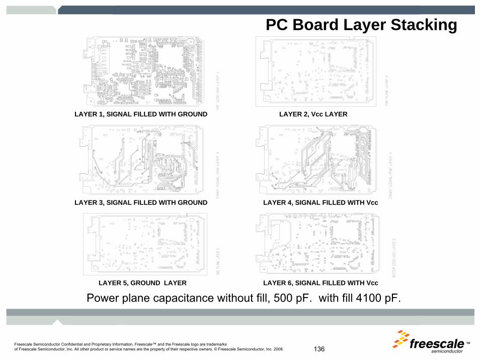
PC Board Layer Stacking
Power plane capacitance without fill, 500 pF. with fill 4100 pF.
LAYER 1, SIGNAL FILLED WITH GROUND LAYER 2, Vcc LAYER
LAYER 3, SIGNAL FILLED WITH GROUND LAYER 4, SIGNAL FILLED WITH Vcc
LAYER 6, SIGNAL FILLED WITH VccLAYER 5, GROUND LAYER

TMFreescale Semiconductor Confidential and Proprietary Information. Freescale™ and the Freescale logo are trademarksof Freescale Semiconductor, Inc. All other product or service names are the property of their respective owners. © Freescale Semiconductor, Inc. 2008. 137
PC Board Layer Stacking EMISSIONS TEST RESULTS WITH AND W ITHOUT SIGNAL PLANE FILLS
0
5
10
15
20
25
30
35
40
45
30 40 50 60 80
80.2
110
120
130
140
150
160
180
200
225
250
275
300
325
350
375
400
425
450
500
550
600
700
800
900
1000
FREQUENCY (Mhz)
EM
ISS
ION
S (d
buV
/M)
CISPRB LIMIT
Dark Green Bars are Unit w/o Power Plane Fills.
(From Speeding Edge, Spring 2001)
Light Green Bars are Unit with Power Plane Fills.

TMFreescale Semiconductor Confidential and Proprietary Information. Freescale™ and the Freescale logo are trademarksof Freescale Semiconductor, Inc. All other product or service names are the property of their respective owners. © Freescale Semiconductor, Inc. 2008. 138
PC Board Layer Stacking
Four(4) Layer Designs
(A) ----Ground----- (B) ---Sig/Poured Pwr-------Sig/Pwr----- --------Ground---------
----Sig/Pwr----- --------Ground-------------Ground----- ---Sig/Poured Pwr---

TMFreescale Semiconductor Confidential and Proprietary Information. Freescale™ and the Freescale logo are trademarksof Freescale Semiconductor, Inc. All other product or service names are the property of their respective owners. © Freescale Semiconductor, Inc. 2008. 139
PC Board Layer Stacking
Six(6) Layer Designs
-----Power------ ----Sig/Pwr--------Sig/Gnd----- ----Ground----------Power------ ----Sig/Pwr--------Ground------ ----Ground---------Sig/Pwr----- -----Power----------Ground------ ----Sig/Gnd----

TMFreescale Semiconductor Confidential and Proprietary Information. Freescale™ and the Freescale logo are trademarksof Freescale Semiconductor, Inc. All other product or service names are the property of their respective owners. © Freescale Semiconductor, Inc. 2008. 140
PC Board Layer Stacking
Six(6) Layer Designs to AVOID
-----Signal------ -----Signal----------Signal------ -----Power---------Ground------ -----Signal-----------Power------ -----Signal-----------Signal------ ----Ground----------Signal------ -----Signal------

TMFreescale Semiconductor Confidential and Proprietary Information. Freescale™ and the Freescale logo are trademarksof Freescale Semiconductor, Inc. All other product or service names are the property of their respective owners. © Freescale Semiconductor, Inc. 2008. 141
PC Board Layer Stacking
Six(6) Layer Designs
-Short Sig/Pwr- ----Sig/Pwr---------Sig/Gnd----- ----Ground----------Power------ ----Sig/Pwr---------Ground------ ----Sig/Gnd---------Sig/Pwr----- -----Power-------Short Sig/Gnd- ----Sig/Gnd-----

TMFreescale Semiconductor Confidential and Proprietary Information. Freescale™ and the Freescale logo are trademarksof Freescale Semiconductor, Inc. All other product or service names are the property of their respective owners. © Freescale Semiconductor, Inc. 2008. 142
PC Board Layer Stacking
Eight(8) Layer Designs
----Signal----- ---Sig/Pwr-------Ground----- ---Ground---------Signal----- ---Sig/Pwr--------Power----- ---Ground--------Ground----- ----Power---------Signal----- ---Sig/Gnd-------Ground----- ----Power---------Signal----- ---Sig/Gnd----

TMFreescale Semiconductor Confidential and Proprietary Information. Freescale™ and the Freescale logo are trademarksof Freescale Semiconductor, Inc. All other product or service names are the property of their respective owners. © Freescale Semiconductor, Inc. 2008. 143
PC Board Layer Stacking
Eight(8) Layer Designs to AVOID
----Signal----- ----Signal----- ----Signal---------Signal----- ----Signal----- ----Power---------Signal----- ----Power----- ----Signal---------Power----- ----Signal----- ----Signal--------Ground---- ----Signal----- ----Signal---------Signal----- ---Ground----- ----Signal---------Signal----- ----Signal------ ---Ground---------Signal----- ----Signal------ ----Signal-----

TMFreescale Semiconductor Confidential and Proprietary Information. Freescale™ and the Freescale logo are trademarksof Freescale Semiconductor, Inc. All other product or service names are the property of their respective owners. © Freescale Semiconductor, Inc. 2008. 144
PC Board Layer Stacking
Gap vs Impedance(w/Soldermask)
Effect of Co-Planar Copper Pour
Gap (mils) Impedance5 456 477 49
- 8 509 50
10 51
Gap (mils) Impedance11 5112 5213 5214 5215 52
No Co-Pl CU 53
6
5 Er - 4.2

TMFreescale Semiconductor Confidential and Proprietary Information. Freescale™ and the Freescale logo are trademarksof Freescale Semiconductor, Inc. All other product or service names are the property of their respective owners. © Freescale Semiconductor, Inc. 2008. 145
PC Board Layer Stacking
►Basics:• Signal Layers placed One Dielectric Layer away from
Plane gives Best Control of Impedance.
• Outer Layers have Poorest Impedance Control and Poorest Cross Talk Control.
• Plane Pairs give Highest Interplane Capacitance (Critical for EMI). Use Copper Pour!!!

TMFreescale Semiconductor Confidential and Proprietary Information. Freescale™ and the Freescale logo are trademarksof Freescale Semiconductor, Inc. All other product or service names are the property of their respective owners. © Freescale Semiconductor, Inc. 2008. 146