sgls310d – july 2005– revised february 2012 · pdf file8 tps40055-ep sgls310d...
TRANSCRIPT

8TPS40055-EP
www.ti.com SGLS310D –JULY 2005–REVISED FEBRUARY 2012
WIDE-INPUT SYNCHRONOUS BUCK CONTROLLERCheck for Samples: TPS40055-EP
1FEATURES APPLICATIONS2• Operating Input Voltage 8 V to 40 V • Power Modules• Input Voltage Feed-Forward Compensation • Networking/Telecom• < 1 % Internal 0.7-V Reference • Industrial/Servers• Programmable Fixed-Frequency Up to 1-MHz
DESCRIPTIONVoltage Mode ControllerThe TPS40055 is a family of high-voltage, wide input• Internal Gate Drive Outputs for High-Side and(8 V to 40 V), synchronous, step-down converters.Synchronous N-Channel MOSFETsThe TPS40055 family offers design flexibility with a
• 16-Pin PowerPAD™ Package (θJC = 25°C/W) variety of user programmable functions, includingsoft-start, UVLO, operating frequency, voltage feed-• Thermal Shutdownforward, high-side current limit, and loop• Externally Synchronizablecompensation.
• Programmable High-Side Sense Short-CircuitThe TPS40055 are also synchronizable to an externalProtectionsupply. The TPS40055 incorporates MOSFET gate• Programmable Closed-Loop Soft-Start drivers for external N-channel high-side and
• TPS40055 Source/Sink synchronous rectifier (SR) MOSFETs. Gate drivelogic incorporates anti-cross conduction circuitry to
SUPPORTS DEFENSE, AEROSPACE, prevent simultaneous high-side and synchronousrectifier conduction.AND MEDICAL APPLICATIONS
• Controlled Baseline The TPS40055 uses voltage feed-forward controltechniques to provide good line regulation over the• One Assembly/Test Sitewide (4:1) input voltage range and fast response to
• One Fabrication Site input line transients with near constant gain with input• Available in Military (–55°C/125°C) variation which eases loop compensation. The
externally programmable current limit provides pulse-Temperature Range (1)
by-pulse current limit, as well as a hiccup mode• Extended Product Life Cycleoperation utilizing an internal fault counter for longer
• Extended Product-Change Notification duration overloads.• Product Traceability(1) Additional temperature ranges available - contact factory
1
Please be aware that an important notice concerning availability, standard warranty, and use in critical applications ofTexas Instruments semiconductor products and disclaimers thereto appears at the end of this data sheet.
2PowerPAD is a trademark of Texas Instruments.
PRODUCTION DATA information is current as of publication date. Copyright © 2005–2012, Texas Instruments IncorporatedProducts conform to specifications per the terms of the TexasInstruments standard warranty. Production processing does notnecessarily include testing of all parameters.

TPS40055
TPS40055-EP
SGLS310D –JULY 2005–REVISED FEBRUARY 2012 www.ti.com
SIMPLIFIED APPLICATION DIAGRAM
This integrated circuit can be damaged by ESD. Texas Instruments recommends that all integrated circuits be handled withappropriate precautions. Failure to observe proper handling and installation procedures can cause damage.
ESD damage can range from subtle performance degradation to complete device failure. Precision integrated circuits may be moresusceptible to damage because very small parametric changes could cause the device not to meet its published specifications.
ORDERING INFORMATION (1)
TA APPLICATION (2) PACKAGE (3) (4) PART NUMBER
–55°C to 125°C SOURCE/SINK Plastic HTSSOP (PWP) TPS40055MPWPREP
(1) For the most current package and ordering information, see the Package Option Addendum at the end of this document, or see the TIWeb site at www.ti.com.
(2) See Application Information section.(3) Package drawings, standard packing quantities, thermal data, symbolization, and PCB design guidelines are available at
www.ti.com/sc/package.(4) The PWP package is also available taped and reeled. Add an R suffix to the device type. See the application section of the data sheet
for PowerPAD drawing and layout information.
2 Submit Documentation Feedback Copyright © 2005–2012, Texas Instruments Incorporated
Product Folder Link(s): TPS40055-EP

TPS40055-EP
www.ti.com SGLS310D –JULY 2005–REVISED FEBRUARY 2012
ABSOLUTE MAXIMUM RATINGSover operating free-air temperature range (unless otherwise noted) (1)
VALUE / UNIT
VIN 45 V
VFB, SS, SYNC –0.3 V to 6 V
VIN Input voltage range SW –0.3 V to 45 V
SW, transient < 50 ns –2.5 V
KFF, with IIN(max) = –5 mA –0.3 V to 11 V
VOUT Output voltage range COMP, RT, SS –0.3 V to 6 V
IIN Input current KFF 5 mA
IOUT Output current RT 200 µA
TJ Operating junction temperature range –55°C to 140°C
Tstg Storage temperature (2) –55°C to 150°C
Lead temperature 1,6 mm (1/16 inch) from case for 10 seconds 260°C
TJC Thermal resistance junction-to-case 26.6°C/W
TJA Thermal resistance junction-to-ambient (3) (4) 36.5°C/W
TJP Thermal resistance junction-to-bottom of thermal pad (3) 2.1°C/W
φJT Junction-to-top thermal parameter (3) (4) 0.848°C/W
(1) Stresses beyond those listed under absolute maximum ratings may cause permanent damage to the device. These are stress ratingsonly, and functional operation of the device at these or any other conditions beyond those indicated under recommended operatingconditions is not implied. Exposure to absolute-maximum-rated conditions for extended periods may affect device reliability.
(2) Long-term high-temperature storage and/or extended use at maximum recommended operating conditions may result in reduced overalldevice life. See http://www.ti.com/ep_quality for additional information on enhanced plastic packaging.
(3) See technical brief SLMA002 - PowerPAD Thermally Enhanced Package(http://www-s.ti.com/sc/techlit/slma002).(4) Tested in accordance with the thermal metric definitions of EIA/JESD51-5.
RECOMMENDED OPERATING CONDITIONSMIN NOM MAX UNIT
VI Input voltage 8 40 V
TA Operating free-air temperature –55 125 °C
ELECTRICAL CHARACTERISTICSTA = –55°C to 125°C, VIN = 24 Vdc, RT = 90.9 kΩ, IKFF = 150 µA, fSW = 500 kHz, all parameters at zero power dissipation(unless otherwise noted)
PARAMETER TEST CONDITIONS MIN TYP MAX UNIT
INPUT SUPPLY
VIN Input voltage range, VIN 8 40 V
OPERATING CURRENT
IDD Quiescent current Output drivers not switching, VFB ≥ 1.5 3.3 mA0.75 V
BP5
VBP5 Output voltage IOUT ≤ 1 mA 4.7 5 5.3 V
OSCILLATOR/RAMP GENERATOR (1)
fOSC Accuracy 8 V ≤ VIN ≤ 40 V 465 520 585 kHz
VRAMP PWM ramp voltage (2) VPEAK – VVAL 2 V
VIH High-level input voltage, SYNC 2 5 V
VIL Low-level input voltage, SYNC 0.8 V
ISYNC Input current, SYNC 5 11 µA
Pulse width, SYNC 50 ns
VRT RT voltage 2.37 2.5 2.59 V
(1) IKFF increases with SYNC frequency, IKFF decreases with maximum duty cycle.(2) Ensured by design. Not production tested.
Copyright © 2005–2012, Texas Instruments Incorporated Submit Documentation Feedback 3
Product Folder Link(s): TPS40055-EP

TPS40055-EP
SGLS310D –JULY 2005–REVISED FEBRUARY 2012 www.ti.com
ELECTRICAL CHARACTERISTICS (continued)TA = –55°C to 125°C, VIN = 24 Vdc, RT = 90.9 kΩ, IKFF = 150 µA, fSW = 500 kHz, all parameters at zero power dissipation(unless otherwise noted)
PARAMETER TEST CONDITIONS MIN TYP MAX UNIT
VFB = 0 V, fSW ≤ 500 kHz 84% 94%Maximum duty cycle
VFB = 0 V, 500 kHz ≤ fSW ≤ 1 MHz (2) 80%
Minimum duty cycle VFB ≥ 0.75 V 0%
VKFF Feed-forward voltage 3.35 3.48 3.7 V
IKFF Feed-forward current operating range (2) 20 1200 µA
SOFT START
ISS Soft-start source current 1.2 2.35 3.6 µA
VSS Soft-start clamp voltage 3.7 V
tDSCH Discharge time CSS = 220 pF 1.4 2.2 3.4 µs
tSS Soft-start time CSS = 220 pF, 0 V ≤ VSS ≤ 1.6 V 102 150 230 µs
BP10
VBP10 Output voltage IOUT ≤ 1 mA 8.9 9.6 10.45 V
ERROR AMPLIFIER
8 V ≤ VIN ≤ 40 V, TA = 25°C 0.698 0.7 0.704
8 V ≤ VIN ≤ 40 V, 0°C ≤ TA ≤ 125°C 0.689 0.7 0.717VFB Feedback input voltage V8 V ≤ VIN ≤ 40 V, –55°C ≤ TA ≤ 0.689 0.7 0.719125°C
GBW Gain bandwidth (3) 2.8 5 MHz
AVOL Open loop gain 40 80 dB
IOH High-level output source current 1.85 4mA
IOL Low-level output source current 1.95 4
VOH High-level output voltage ISOURCE = 500 µA 3.1 3.5V
VOL Low-level output voltage ISINK = 500 µA 0.2 0.37
IBIAS Input bias current VFB = 0.7 V 100 220 nA
CURRENT LIMIT
ISINK Current limit sink current 7.5 10 12.2 µA
VILIM = 23.7 V, VSW = (VILIM – 0.5 V) 300Propagation delay to output ns
VILIM = 23.7 V, VSW = (VILIM – 2 V) 200
tON Switch leading-edge blanking pulse time (3) 100 ns
tOFF Off time during a fault 7 cycles
VILIM = 23.6 V, TA = 25°C –115 –70 –50
VILIM = 23.6 V, 0°C ≤ TA ≤ 125°C –155 –38
VILIM = 23.6 V, –55°C ≤ TA ≤ 125°C –155 –10VOS Offset voltage SW vs ILIM mV
VILIM = 11.6 V, TA = 25°C –118 –43
VILIM = 11.6 V, 0°C ≤ TA ≤ 125°C –160 –45
VILIM = 11.6 V, TA = –55°C to 125°C –160 –15
OUTPUT DRIVER
tLRISE Low-side driver rise time 48 110CLOAD = 2200 pF ns
tLFALL Low-side driver fall time 24 58
tHRISE High-side driver rise time 48 105CLOAD = 2200 pF, (HDRV – SW) ns
tHFALL High-side driver fall time 36 82
VOH High-level output voltage, HDRV IHDRV = –0.1 A (HDRV - SW) BOOST BOOST V–1.9 –1
VOL Low-level output voltage, HDRV IHDRV = 0.1 A (HDRV - SW) 0.85 V
(3) Ensured by design. Not production tested.
4 Submit Documentation Feedback Copyright © 2005–2012, Texas Instruments Incorporated
Product Folder Link(s): TPS40055-EP
TPS40055-EP
www.ti.com SGLS310D –JULY 2005–REVISED FEBRUARY 2012
ELECTRICAL CHARACTERISTICS (continued)TA = –55°C to 125°C, VIN = 24 Vdc, RT = 90.9 kΩ, IKFF = 150 µA, fSW = 500 kHz, all parameters at zero power dissipation(unless otherwise noted)
PARAMETER TEST CONDITIONS MIN TYP MAX UNIT
VOH High-level output voltage, LDRV ILDRV = –0.1 A BP10 BP10 V–1.8 –1
VOL Low-level output voltage, LDRV ILDRV = 0.1 A 0.6 V
Minimum controllable pulse width 100 160 ns
SS/SD SHUTDOWN
VSD Shutdown threshold voltage Outputs off 85 125 170 mV
VEN Device active threshold voltage 180 210 260 mV
BOOST REGULATOR
VBOOST Output voltage VIN = 24 V 30.8 32.2 33.9 V
SW NODE
ILEAK Leakage current (4) 35 µA
THERMAL SHUTDOWN
Shutdown temperature (4) 165TSD °C
Hysteresis (4) 20
UVLO
VUVLO KFF programmable threshold voltage RKFF = 28.7 kΩ 6.85 7.5 7.95
UVLO, fixed 7.05 7.5 7.9 VVDD
UVLO, hysteresis 0.46
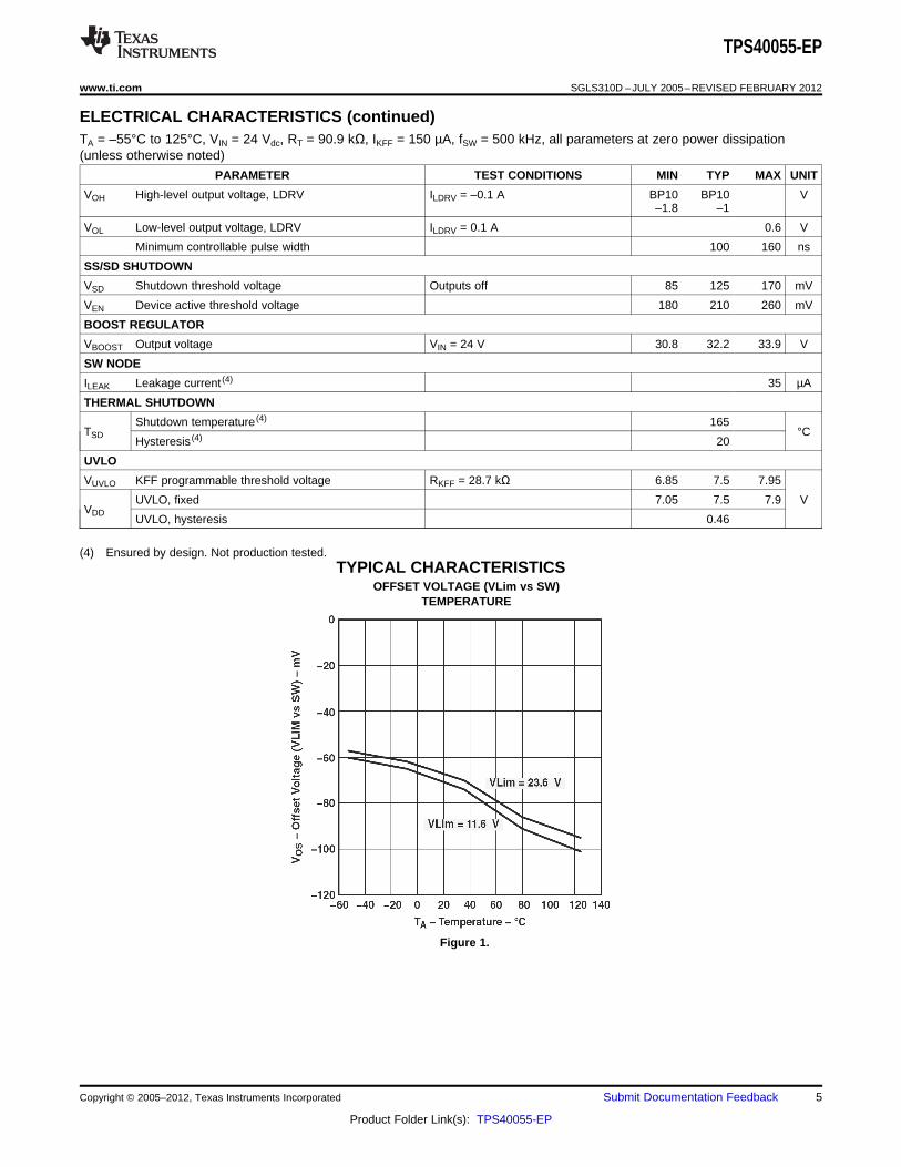
(4) Ensured by design. Not production tested.TYPICAL CHARACTERISTICS
OFFSET VOLTAGE (VLim vs SW)TEMPERATURE
Figure 1.
Copyright © 2005–2012, Texas Instruments Incorporated Submit Documentation Feedback 5
Product Folder Link(s): TPS40055-EP

TPS40055-EP
SGLS310D –JULY 2005–REVISED FEBRUARY 2012 www.ti.com
DEVICE INFORMATION
(1) For more information on the PWP package, see the Texas Instruments Technical Brief (SLMA002)
(2) PowerPAD heat slug must be connected to SGND (pin 5) or electrically isolated from all other pins.
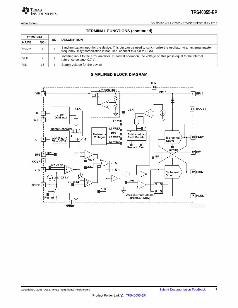
TERMINAL FUNCTIONSTERMINAL
I/O DESCRIPTIONNAME NO.
Gate drive voltage for the high side N-channel MOSFET. The BOOST voltage is 9 V greater than the inputBOOST 14 O voltage. A 0.1-µF ceramic capacitor should be connected from this pin to the drain of the lower MOSFET.
5-V reference. This pin should be bypassed to ground with a 0.1-µF ceramic capacitor. This pin may be usedBP5 3 O with an external dc load of 1 mA or less.
10-V reference used for gate drive of the N-channel synchronous rectifier. This pin should be bypassed by a 1-BP10 11 O µF ceramic capacitor. This pin may be used with an external dc load of 1 mA or less.
Output of the error amplifier, input to the PWM comparator. A feedback network is connected from this pin toCOMP 8 O the VFB pin to compensate the overall loop. The COMP pin is internally clamped above the peak of the ramp to
improve large signal transient response.
Floating gate drive for the high-side N-channel MOSFET. This pin switches from BOOST (MOSFET on) to SWHDRV 13 O (MOSFET off).
Current limit pin used to set the overcurrent threshold. An internal current sink from this pin to ground sets aILIM 16 I voltage drop across an external resistor connected from this pin to VCC. The voltage on this pin is compared to
the voltage drop (VIN -SW) across the high side MOSFET during conduction.
A resistor is connected from this pin to VIN to program the amount of voltage feed-forward. The current fed intoKFF 1 I this pin is internally divided and used to control the slope of the PWM ramp.
Gate drive for the N-channel synchronous rectifier. This pin switches from BP10 (MOSFET on) to groundLDRV 10 O (MOSFET off).
Power ground reference for the device. There should be a low-impedance path from this pin to the source(s) ofPGND 9 – the lower MOSFET(s).
RT 2 I A resistor is connected from this pin to ground to set the internal oscillator and switching frequency.
SGND 5 – Signal ground reference for the device
Soft-start programming pin. A capacitor connected from this pin to ground programs the soft-start time. Thecapacitor is charged with an internal current source of 2.3 µA. The resulting voltage ramp on the SS pin is usedas a second non-inverting input to the error amplifier. The output voltage begins to rise when VSS/SD isapproximately 0.85 V. The output continues to rise and reaches regulation when VSS/SD is approximatelySS/SD 6 I 1.55 V. The controller is considered shut down when VSS/SD is 125 mV or less. All internal circuitry is inactive.The internal circuitry is enabled when VSS/SD is 210 mV or greater. When VSS/SD is less than approximately0.85 V, the outputs cease switching and the output voltage (VOUT) decays while the internal circuitry remainsactive.
SW 12 I This pin is connected to the switched node of the converter and used for overcurrent sensing.
6 Submit Documentation Feedback Copyright © 2005–2012, Texas Instruments Incorporated
Product Folder Link(s): TPS40055-EP
0.7 VREF
0.85 V
TPS40055-EP
www.ti.com SGLS310D –JULY 2005–REVISED FEBRUARY 2012
TERMINAL FUNCTIONS (continued)
TERMINALI/O DESCRIPTION
NAME NO.
Synchronization input for the device. This pin can be used to synchronize the oscillator to an external masterSYNC 4 I frequency. If synchronization is not used, connect this pin to SGND.
Inverting input to the error amplifier. In normal operation, the voltage on this pin is equal to the internalVFB 7 I reference voltage, 0.7 V.
VIN 15 I Supply voltage for the device
SIMPLIFIED BLOCK DIAGRAM
Copyright © 2005–2012, Texas Instruments Incorporated Submit Documentation Feedback 7
Product Folder Link(s): TPS40055-EP
TPS40055-EP
SGLS310D –JULY 2005–REVISED FEBRUARY 2012 www.ti.com
APPLICATION INFORMATION
The TPS40055 allows the user to optimize the PWM controller to the specific application.
The TPS40055 is the controller of choice for synchronous buck designs, which includes most applications. It hastwo quadrant operations and will source or sink output current. This provides the best transient response.
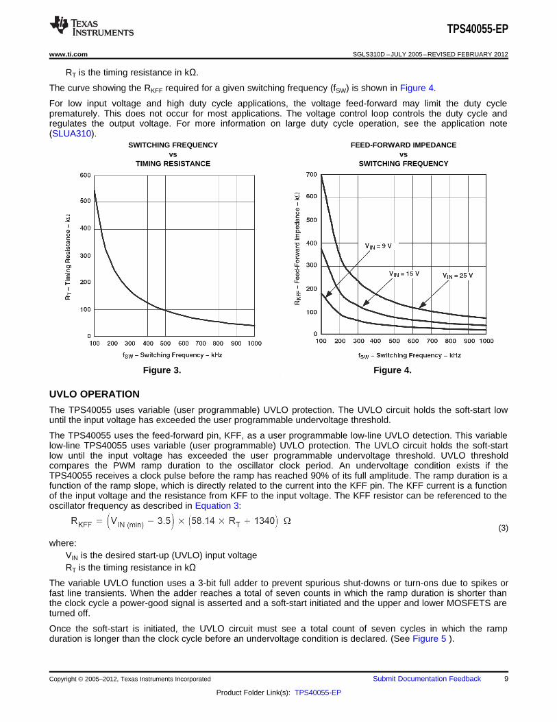
SETTING THE SWITCHING FREQUENCY (PROGRAMMING THE CLOCK OSCILLATOR)
The TPS40055 has independent clock oscillator and ramp generator circuits. The clock oscillator serves as themaster clock to the ramp generator circuit. The switching frequency, fSW in kHz, of the clock oscillator is set by asingle resistor (RT) to ground. The clock frequency is related to RT, in kΩ by Equation 1 and the relationship ischarted in Figure 3.
(1)
PROGRAMMING THE RAMP GENERATOR CIRCUIT
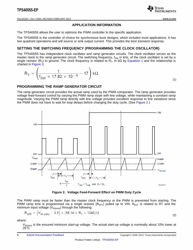
The ramp generator circuit provides the actual ramp used by the PWM comparator. The ramp generator providesvoltage feed-forward control by varying the PWM ramp slope with line voltage, while maintaining a constant rampmagnitude. Varying the PWM ramp directly with line voltage provides excellent response to line variations sincethe PWM does not have to wait for loop delays before changing the duty cycle. (See Figure 2 ).
Figure 2. Voltage Feed-Forward Effect on PWM Duty Cycle
The PWM ramp must be faster than the master clock frequency or the PWM is prevented from starting. ThePWM ramp time is programmed via a single resistor (RKFF) pulled up to VIN. RKFF is related to RT and theminimum input voltage (VIN(min)) through the following:
(2)
where:VIN(min) is the ensured minimum start-up voltage. The actual start-up voltage is nominally about 10% lower at25°C.
8 Submit Documentation Feedback Copyright © 2005–2012, Texas Instruments Incorporated
Product Folder Link(s): TPS40055-EP
TPS40055-EP
www.ti.com SGLS310D –JULY 2005–REVISED FEBRUARY 2012
RT is the timing resistance in kΩ.
The curve showing the RKFF required for a given switching frequency (fSW) is shown in Figure 4.
For low input voltage and high duty cycle applications, the voltage feed-forward may limit the duty cycleprematurely. This does not occur for most applications. The voltage control loop controls the duty cycle andregulates the output voltage. For more information on large duty cycle operation, see the application note(SLUA310).
SWITCHING FREQUENCY FEED-FORWARD IMPEDANCEvs vs
TIMING RESISTANCE SWITCHING FREQUENCY
Figure 3. Figure 4.
UVLO OPERATION
The TPS40055 uses variable (user programmable) UVLO protection. The UVLO circuit holds the soft-start lowuntil the input voltage has exceeded the user programmable undervoltage threshold.
The TPS40055 uses the feed-forward pin, KFF, as a user programmable low-line UVLO detection. This variablelow-line TPS40055 uses variable (user programmable) UVLO protection. The UVLO circuit holds the soft-startlow until the input voltage has exceeded the user programmable undervoltage threshold. UVLO thresholdcompares the PWM ramp duration to the oscillator clock period. An undervoltage condition exists if theTPS40055 receives a clock pulse before the ramp has reached 90% of its full amplitude. The ramp duration is afunction of the ramp slope, which is directly related to the current into the KFF pin. The KFF current is a functionof the input voltage and the resistance from KFF to the input voltage. The KFF resistor can be referenced to theoscillator frequency as described in Equation 3:
(3)
where:VIN is the desired start-up (UVLO) input voltageRT is the timing resistance in kΩ
The variable UVLO function uses a 3-bit full adder to prevent spurious shut-downs or turn-ons due to spikes orfast line transients. When the adder reaches a total of seven counts in which the ramp duration is shorter thanthe clock cycle a power-good signal is asserted and a soft-start initiated and the upper and lower MOSFETS areturned off.
Once the soft-start is initiated, the UVLO circuit must see a total count of seven cycles in which the rampduration is longer than the clock cycle before an undervoltage condition is declared. (See Figure 5 ).
Copyright © 2005–2012, Texas Instruments Incorporated Submit Documentation Feedback 9
Product Folder Link(s): TPS40055-EP

TPS40055-EP
SGLS310D –JULY 2005–REVISED FEBRUARY 2012 www.ti.com
Figure 5. Undervoltage Lockout Operation
The tolerance on the UVLO set point also affects the maximum duty cycle achievable. If the UVLO starts thedevice at 10% below the nominal start up voltage, the maximum duty cycle is reduced approximately 10% at thenominal start up voltage.
The impedance of the input voltage can cause the input voltage, at the controller, to sag when the converterstarts to operate and draw current from the input source. Therefore, there is voltage hysteresis that preventsnuisance shutdowns at the UVLO point. With RT chosen to select the operating frequency and RKFF chosen toselect the start-up voltage, the approximate amount of hysteresis voltage is shown in Figure 7.
Figure 6. UNDERVOLTAGE LOCKOUT THRESHOLDvs
HYSTERESIS
Figure 7.
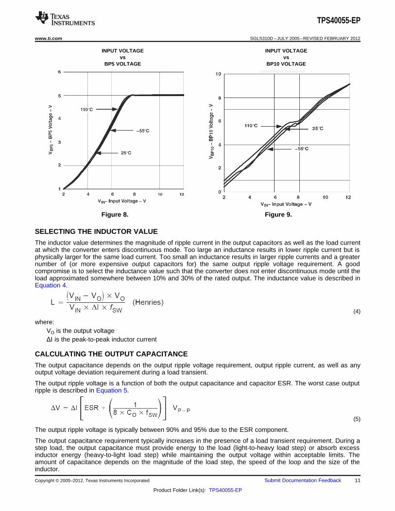
BP5 AND BP10 INTERNAL VOLTAGE REGULATORS
Start-up characteristics of the BP5 and BP10 regulators over different temperature ranges are shown in Figure 8and Figure 9. Slight variations in the BP5 occurs dependent upon the switching frequency. Variation in the BP10regulation characteristics is also based on the load presented by switching the external MOSFETs.
10 Submit Documentation Feedback Copyright © 2005–2012, Texas Instruments Incorporated
Product Folder Link(s): TPS40055-EP
TPS40055-EP
www.ti.com SGLS310D –JULY 2005–REVISED FEBRUARY 2012
INPUT VOLTAGE INPUT VOLTAGEvs vs
BP5 VOLTAGE BP10 VOLTAGE
Figure 8. Figure 9.
SELECTING THE INDUCTOR VALUE
The inductor value determines the magnitude of ripple current in the output capacitors as well as the load currentat which the converter enters discontinuous mode. Too large an inductance results in lower ripple current but isphysically larger for the same load current. Too small an inductance results in larger ripple currents and a greaternumber of (or more expensive output capacitors for) the same output ripple voltage requirement. A goodcompromise is to select the inductance value such that the converter does not enter discontinuous mode until theload approximated somewhere between 10% and 30% of the rated output. The inductance value is described inEquation 4.
(4)
where:VO is the output voltageΔI is the peak-to-peak inductor current
CALCULATING THE OUTPUT CAPACITANCE
The output capacitance depends on the output ripple voltage requirement, output ripple current, as well as anyoutput voltage deviation requirement during a load transient.
The output ripple voltage is a function of both the output capacitance and capacitor ESR. The worst case outputripple is described in Equation 5.
(5)
The output ripple voltage is typically between 90% and 95% due to the ESR component.
The output capacitance requirement typically increases in the presence of a load transient requirement. During astep load, the output capacitance must provide energy to the load (light-to-heavy load step) or absorb excessinductor energy (heavy-to-light load step) while maintaining the output voltage within acceptable limits. Theamount of capacitance depends on the magnitude of the load step, the speed of the loop and the size of theinductor.
Copyright © 2005–2012, Texas Instruments Incorporated Submit Documentation Feedback 11
Product Folder Link(s): TPS40055-EP

TPS40055-EP
SGLS310D –JULY 2005–REVISED FEBRUARY 2012 www.ti.com
Stepping the load from a heavy load to a light load results in an output overshoot. Excess energy stored in theinductor must be absorbed by the output capacitance. The energy stored in the inductor is described inEquation 6.
(6)
where:
(7)
IOH is the output current under heavy load conditionsIOL is the output current under light load conditions
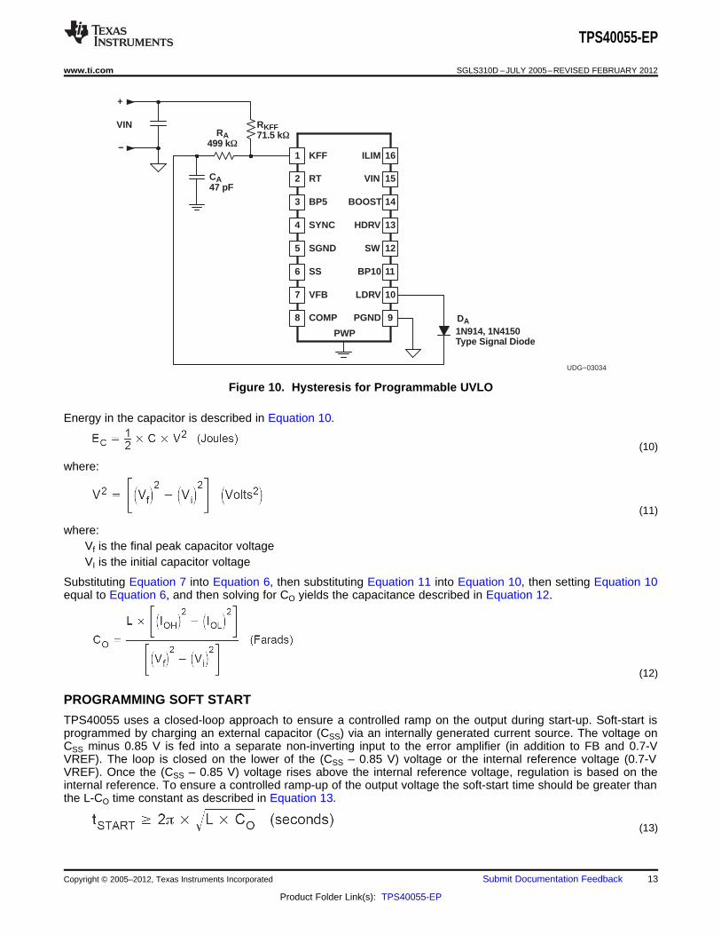
Some applications may require an additional circuit to prevent false restarts at the UVLO voltage level. Thisapplies to applications which have high impedance on the input voltage line or which have excessive ringing onthe VIN line. The input voltage impedance can cause the input voltage to sag enough at start-up to cause aUVLO shutdown and subsequent restart. Excessive ringing can also affect the voltage seen by the device andcause a UVLO shutdown and restart. A simple external circuit provides a selectable amount of hysteresis toprevent the nuisance UVLO shutdown.
Assuming a hysteresis current of 10% IKFF and the peak detector charges to 8 V and VIN(min) = 10 V, the value ofRA is calculated by Equation 8 using a RKFF = 71.5 kΩ.
(8)
CA is chosen to maintain the peak voltage between switching cycles. To keep the capacitor charge from drooping0.1 V, or from 8 V to 7.9 V.
(9)
The value of CA may calculate to less than 10 pF, but some standard value up to 47 pF works adequately. Thediode can be a small signal switching diode or Schottky rated for more then 20 V. Figure 10 illustrates a typicalimplementation using a small switching diode.
The tolerance on the UVLO set point also affects the maximum duty cycle achievable. If the UVLO starts thedevice at 10% below the nominal start up voltage, the maximum duty cycle is reduced approximately 10% at thenominal start up voltage.
12 Submit Documentation Feedback Copyright © 2005–2012, Texas Instruments Incorporated
Product Folder Link(s): TPS40055-EP
UDG−03034
DA
CA47 pF
RA499 k
RKFF71.5 k
1
2
3
4
16
15
14
13
ILIM
VIN
BOOST
HDRV
KFF
RT
BP5
SYNC
5
6
7
8
12
11
10
9
SW
BP10
LDRV
PGND
SGND
SS
VFB
COMP
VIN
+
−
PWP 1N914, 1N4150Type Signal Diode
TPS40055-EP
www.ti.com SGLS310D –JULY 2005–REVISED FEBRUARY 2012
Figure 10. Hysteresis for Programmable UVLO
Energy in the capacitor is described in Equation 10.
(10)
where:
(11)
where:Vf is the final peak capacitor voltageVI is the initial capacitor voltage
Substituting Equation 7 into Equation 6, then substituting Equation 11 into Equation 10, then setting Equation 10equal to Equation 6, and then solving for CO yields the capacitance described in Equation 12.
(12)
PROGRAMMING SOFT START
TPS40055 uses a closed-loop approach to ensure a controlled ramp on the output during start-up. Soft-start isprogrammed by charging an external capacitor (CSS) via an internally generated current source. The voltage onCSS minus 0.85 V is fed into a separate non-inverting input to the error amplifier (in addition to FB and 0.7-VVREF). The loop is closed on the lower of the (CSS – 0.85 V) voltage or the internal reference voltage (0.7-VVREF). Once the (CSS – 0.85 V) voltage rises above the internal reference voltage, regulation is based on theinternal reference. To ensure a controlled ramp-up of the output voltage the soft-start time should be greater thanthe L-CO time constant as described in Equation 13.
(13)
Copyright © 2005–2012, Texas Instruments Incorporated Submit Documentation Feedback 13
Product Folder Link(s): TPS40055-EP

TPS40055-EP
SGLS310D –JULY 2005–REVISED FEBRUARY 2012 www.ti.com
There is a direct correlation between tSTART and the input current required during start-up. The faster tSTART, thehigher the input current required during start-up. This relationship is describe in more detail in the section titled,Programming the Current Limit which follows. The soft-start capacitance, CSS, is described in Equation 14.
(14)
For applications in which the VIN supply ramps up slowly, (typically between 50 ms and 100 ms) it may benecessary to increase the soft-start time to between approximately 2 ms and 5 ms to prevent nuisance UVLOtripping. The soft-start time should be longer than the time that the VIN supply transitions between 6 V and 7 V.
PROGRAMMING CURRENT LIMIT
The TPS40055 uses a two-tier approach for overcurrent protection. The first tier is a pulse-by-pulse protectionscheme. Current limit is implemented on the high-side MOSFET by sensing the voltage drop across theMOSFET when the gate is driven high. The MOSFET voltage is compared to the voltage dropped across aresistor connected from VIN pin to the ILIM pin when driven by a constant current sink. If the voltage drop acrossthe MOSFET exceeds the voltage drop across the ILIM resistor, the switching pulse is immediately terminated.The MOSFET remains off until the next switching cycle is initiated.
The second tier consists of a fault counter. The fault counter is incremented on an overcurrent pulse anddecremented on a clock cycle without an overcurrent pulse. When the counter reaches seven, a restart is issuedand seven soft-start cycles are initiated. Both the upper and lower MOSFETs are turned off during this period.The counter is decremented on each soft-start cycle. When the counter is decremented to zero, the PWM is re-enabled. If the fault has been removed the output starts up normally. If the output is still present, the countercounts seven overcurrent pulses and re-enters the second-tier fault mode. See Figure 11 for typical overcurrentprotection waveforms.
The minimum current limit setpoint (ILIM) depends on tSTART, CO, VO, and the load current at turn-on (IL).
(15)
Figure 11. Typical Current Limit Protection Waveforms
The current limit programming resistor (RILIM) is calculated using Equation 16. Care must be taken in choosingthe values used for VOS and ISINK in the equation. In order to assure the output current at the overcurrent level,the minimum value of ISINK and the maximum value of VOS must be used.
14 Submit Documentation Feedback Copyright © 2005–2012, Texas Instruments Incorporated
Product Folder Link(s): TPS40055-EP
TPS40055-EP
www.ti.com SGLS310D –JULY 2005–REVISED FEBRUARY 2012
(16)
where:ISINK is the current into the ILIM pin and is 7.5 µA, minimumIOC is the overcurrent setpoint which is the dc output current plus one-half of the peak inductor currentVOS is the overcurrent comparator offset and is –20 mV, maximum
SYNCHRONIZING TO AN EXTERNAL SUPPLY
The TPS40055 can be synchronized to an external clock through the SYNC pin. Synchronization occurs on thefalling edge of the SYNC signal. The synchronization frequency should be in the range of 20% to 30% higherthan its programmed free-run frequency. The clock frequency at the SYNC pin replaces the master clockgenerated by the oscillator circuit. Pulling the SYNC pin low programs the TPS40055 to freely run at thefrequency programmed by RT.
The higher synchronization must be factored in when programming the PWM ramp generator circuit. If the PWMramp is interrupted by the SYNC pulse, a UVLO condition is declared and the PWM becomes disabled. Typicallythis is of concern under low-line conditions only. In any case, RKFF needs to be adjusted for the higher switchingfrequency. In order to specify the correct value for RKFF at the synchronizing frequency, calculate a dummy valuefor RT that would cause the oscillator to run at the synchronizing frequency. Do not use this value of RT in thedesign.
(17)
Use the value of RT(dummy) to calculate the value for RKFF.
(18)
This value of RKFF ensures that UVLO is not engaged when operating at the synchronization frequency.RT(dummy) is in kΩ
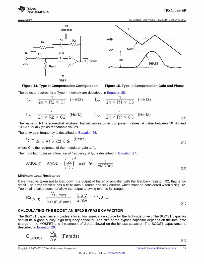
Loop Compensation
Voltage-mode buck-type converters are typically compensated using Type III networks. Since the TPS40055uses voltage feedforward control, the gain of the PWM modulator with voltage feedforward circuit must beincluded. The modulator gain is described in Figure 11, with VIN being the minimum input voltage required tocause the ramp excursion to cover the entire switching period as described in Equation 19.
(19)
Duty cycle (D) varies from 0 to 1 as the control voltage (VC) varies from the minimum ramp voltage to themaximum ramp voltage (VS). Also, for a synchronous buck converter, D = VO / VIN. To get the control voltage tooutput voltage modulator gain in terms of the input voltage and ramp voltage:
(20)
Copyright © 2005–2012, Texas Instruments Incorporated Submit Documentation Feedback 15
Product Folder Link(s): TPS40055-EP

TPS40055-EP
SGLS310D –JULY 2005–REVISED FEBRUARY 2012 www.ti.com
Calculate the Poles and Zeros
For a buck converter using voltage mode control, there is a double pole due to the output L-CO. The double poleis located at the frequency calculated in Equation 21.
(21)
There is also a zero created by the output capacitance (CO) and its associated ESR. The ESR zero is located atthe frequency calculated in Equation 22.
(22)
Calculate the value of RBIAS to set the output voltage (VOUT).
(23)
The maximum crossover frequency (0 dB loop gain) is calculated in Equation 24.
(24)
Typically, fC is selected to be close to the midpoint between the L-CO double pole and the ESR zero. At thisfrequency, the control to output gain has a -2 slope (–40 dB/decade), while the Type III topology has a +1 slope(20 dB/decade), resulting in an overall closed loop –1 slope (–20 dB/decade). Figure 13 shows the modulatorgain, L-C filter, output capacitor ESR zero, and the resulting response to be compensated.
MODULATOR GAINvs
SWITCHING FREQUENCY
Figure 12. PWM Modulator Relationships Figure 13.
A Type III topology, shown in Figure 14, has 2 zero-pole pairs in addition to a pole at the origin. The gain andphase boost of a Type III topology is shown in Figure 15. The two zeros are used to compensate the L-COdouble pole and provide phase boost. The double pole is used to compensate for the ESR zero and providecontrolled gain roll-off. In many cases, the second pole can be eliminated and the amplifier's gain roll-off used toroll-off the overall gain at higher frequencies. Figure 14.
16 Submit Documentation Feedback Copyright © 2005–2012, Texas Instruments Incorporated
Product Folder Link(s): TPS40055-EP
TPS40055-EP
www.ti.com SGLS310D –JULY 2005–REVISED FEBRUARY 2012
Figure 14. Type III Compensation Configuration Figure 15. Type III Compensation Gain and Phase
The poles and zeros for a Type III network are described in Equation 25.
(25)
The value of R1 is somewhat arbitrary, but influences other component values. A value between 50 kΩ and100 kΩ usually yields reasonable values.
The unity gain frequency is described in Equation 26.
(26)
where G is the reciprocal of the modulator gain at fC.
The modulator gain as a function of frequency at fC, is described in Equation 27.
(27)
Minimum Load Resistance
Care must be taken not to load down the output of the error amplifier with the feedback resistor, R2, that is toosmall. The error amplifier has a finite output source and sink current, which must be considered when sizing R2.Too small a value does not allow the output to swing over its full range.
(28)
CALCULATING THE BOOST AN BP10 BYPASS CAPACITOR
The BOOST capacitance provides a local, low impedance source for the high-side driver. The BOOST capacitorshould be a good quality, high-frequency capacitor. The size of the bypass capacitor depends on the total gatecharge of the MOSFET and the amount of droop allowed on the bypass capacitor. The BOOST capacitance isdescribed in Equation 29.
(29)
Copyright © 2005–2012, Texas Instruments Incorporated Submit Documentation Feedback 17
Product Folder Link(s): TPS40055-EP

TPS40055-EP
SGLS310D –JULY 2005–REVISED FEBRUARY 2012 www.ti.com
The 10-V reference pin, BP10V provides energy for both the synchronous MOSFET and the high-side MOSFETvia the BOOST capacitor. Neglecting any efficiency penalty, the BP10V capacitance is described in Equation 30.
(30)
dv/dt INDUCED TURN-ON
MOSFETs are susceptible to dv/dt turn-on particularly in high-voltage (VDS) applications. The turn-on is causedby the capacitor divider that is formed by CGD and CGS. High dv/dt conditions and drain-to-source voltage, on theMOSFET causes current flow through CGD and causes the gate-to-source voltage to rise. If the gate-to-sourcevoltage rises above the MOSFET threshold voltage, the MOSFET turns on, resulting in large shoot-throughcurrents. Therefore, the SR MOSFET should be chosen so that the CGD capacitance is smaller than the CGScapacitance.
HIGH SIDE MOSFET POWER DISSIPATION
The power dissipated in the external high-side MOSFET is comprised of conduction and switching losses. Theconduction losses are a function of the IRMS current through the MOSFET and the RDS(on) of the MOSFET. Thehigh-side MOSFET conduction losses are defined by Equation 31.
(31)
where:TCR is the temperature coefficient of the MOSFET RDS(on)
The TCR varies depending on MOSFET technology and manufacturer, but typically ranges between3500 ppm/°C and 10000 ppm/°C.
The IRMS current for the high side MOSFET is described in Equation 32.
(32)
The switching losses for the high-side MOSFET are described in Equation 33.
(33)
where:IO is the dc-output currenttSW is the switching rise time, typically < 20 nsfSW is the switching frequency
Typical switching waveforms are shown in Figure 16.
18 Submit Documentation Feedback Copyright © 2005–2012, Texas Instruments Incorporated
Product Folder Link(s): TPS40055-EP

UDG−02139
∆I
ANTI−CROSSCONDUCTION
SYNCHRONOUSRECTIFIER ON
BODY DIODECONDUCTION
BODY DIODECONDUCTION
HIGH SIDE ON
ID1
ID2
IO
SW
0
d 1−d
TPS40055-EP
www.ti.com SGLS310D –JULY 2005–REVISED FEBRUARY 2012
Figure 16. Inductor Current and SW Node Waveforms
The maximum allowable power dissipation in the MOSFET is determined by Equation 34.
(34)
where:
(35)
and θJA is the package thermal impedance.
SYNCHRONOUS RECTIFIER MOSFET POWER DISSIPATION
The power dissipated in the synchronous rectifier MOSFET is comprised of three components: RDS(on) conductionlosses, body diode conduction losses, and reverse recovery losses. RDS(on) conduction losses can be found usingEquation 31 and the RMS current through the synchronous rectifier MOSFET is described in Equation 36.
(36)
The body-diode conduction losses are due to forward conduction of the body diode during the anti-crossconduction delay time. The body diode conduction losses are described by Equation 37.
(37)
where:VF is the body diode forward voltagetDELAY is the delay time just before the SW node rises
The 2-multiplier is used because the body diode conducts twice during each cycle (once on the rising edge andonce on the falling edge). The reverse recovery losses are due to the time it takes for the body diode to recoveryfrom a forward bias to a reverse blocking state. The reverse recovery losses are described in Equation 38.
(38)
where:QRR is the reverse recovery charge of the body diode.
Copyright © 2005–2012, Texas Instruments Incorporated Submit Documentation Feedback 19
Product Folder Link(s): TPS40055-EP

TPS40055-EP
SGLS310D –JULY 2005–REVISED FEBRUARY 2012 www.ti.com
The QRR is not always described in a MOSFET's data sheet, but may be obtained from the MOSFET vendor.The total synchronous rectifier MOSFET power dissipation is described in Equation 39.
(39)
TPS40055 POWER DISSIPATION
The power dissipation in the TPS40055 is largely dependent on the MOSFET driver currents and the inputvoltage. The driver current is proportional to the total gate charge, Qg, of the external MOSFETs. Driver power(neglecting external gate resistance)[2] can be calculated from Equation 40.
(40)
And the total power dissipation in the TPS40055, assuming the same MOSFET is selected for both the high-sideand synchronous rectifier is described in Equation 41.
(41)
or
(42)
where:IQ is the quiescent operating current (neglecting drivers)
The maximum power capability of the device's PowerPad package is dependent on the layout as well as air flow.The thermal impedance from junction to air, assuming 2 oz. copper trace and thermal pad with solder and no airflow.
(43)
The maximum allowable package power dissipation is related to ambient temperature by Equation 44.
(44)
Substituting Equation 45 into Equation 41 and solving for fSW yields the maximum operating frequency for theTPS40055. The result is described in Equation 45.
(45)
LAYOUT CONSIDERATIONS
PowerPAD™ PACKAGE
The PowerPAD package provides low thermal impedance for heat removal from the device. The PowerPADderives its name and low thermal impedance from the large bonding pad on the bottom of the device. Formaximum thermal performance, the circuit board must have an area of solder-tinned-copper underneath thepackage. The dimensions of this area depends on the size of the PowerPAD package. For a 16-pin TSSOP(PWP) package, dimensions of the circuit board pad area are 5 mm x 3,4 mm [2]. The dimensions of the packagepad are shown in Figure 17.
20 Submit Documentation Feedback Copyright © 2005–2012, Texas Instruments Incorporated
Product Folder Link(s): TPS40055-EP

TPS40055-EP
www.ti.com SGLS310D –JULY 2005–REVISED FEBRUARY 2012
Thermal vias connect this area to internal or external copper planes and should have a drill diameter sufficientlysmall so that the via hole is effectively plugged when the barrel of the via is plated with copper. This plug isneeded to prevent wicking the solder away from the interface between the package body and the solder-tinnedarea under the device during solder reflow. Drill diameters of 0,33 mm (13 mils) works well when 1-oz copper isplated at the surface of the board while simultaneously plating the barrel of the via. If the thermal vias are notplugged when the copper plating is performed, then a solder mask material should be used to cap the vias with adiameter equal to the via diameter of 0,1 mm minimum. This capping prevents the solder from being wickedthrough the thermal vias and potentially creating a solder void under the package. See the PowerPAD ThermallyEnhanced Package and the mechanical illustration at the end of this document for more information on thePowerPAD package.
Figure 17. PowerPAD Dimensions
MOSFET PACKAGING
MOSFET package selection depends on MOSFET power dissipation and the projected operating conditions. Ingeneral, for a surface-mount applications, the DPAK style package provides the lowest thermal impedance (θJA)and, therefore, the highest power dissipation capability. However, the effectiveness of the DPAK depends onproper layout and thermal management. The θJA specified in the MOSFET data sheet refers to a given copperarea and thickness. In most cases, a lowest thermal impedance of 40°C/W requires one square inch of 2-ouncecopper on a G-10/FR-4 board. Lower thermal impedances can be achieved at the expense of board area. Seethe selected MOSFET's data sheet for more information regarding proper mounting.
GROUNDING AND CIRCUIT LAYOUT CONSIDERATIONS
The TPS40055 provides separate signal ground (SGND) and power ground (PGND) pins. It is important thatcircuit grounds are properly separated. Each ground should consist of a plane to minimize its impedance ifpossible. The high power noisy circuits such as the output, synchronous rectifier, MOSFET driver decouplingcapacitor (BP10), and the input capacitor should be connected to PGND plane at the input capacitor.
Sensitive nodes such as the FB resistor divider, RT, and ILIM should be connected to the SGND plane. TheSGND plane should only make a single point connection to the PGND plane.
Component placement should ensure that bypass capacitors (BP10 and BP5) are located as close as possible totheir respective power and ground pins. Also, sensitive circuits such as FB, RT, and ILIM should not be locatednear high dv/dt nodes such as HDRV, LDRV, BOOST, and the switch node (SW).
Copyright © 2005–2012, Texas Instruments Incorporated Submit Documentation Feedback 21
Product Folder Link(s): TPS40055-EP

TPS40055-EP
SGLS310D –JULY 2005–REVISED FEBRUARY 2012 www.ti.com
DESIGN EXAMPLE
• Input Voltage: 10 Vdc to 24 Vdc• Output voltage: 3.3 V +2% (3.234 ≤ VO ≤ 3.366)• Output current: 8 A (maximum, steady state), 10 A (surge, 10-ms duration, 10% duty cycle maximum)• Output ripple: 33 mVP-P at 8 A• Output load response: 0.3 V => 10% to 90% step load change, from 1 A to 7 A• Operating temperature: -40°C to 85°C• fSW = 300 kHz
1. Calculate maximum and minimum duty cycles
(46)
2. Select switching frequency
The switching frequency is based on the minimum duty cycle ratio and the propagation delay of the current limitcomparator. In order to maintain current limit capability, the on time of the upper MOSFET (tON) must be greaterthan 300 ns (see the Electrical Characteristics table). Therefore,
(47)
(48)
Using 400 ns to provide margin,
(49)
Since the oscillator can vary by 10%, decrease fSW by 10%
(50)
and therefore choose a frequency of 300 kHz.
3. Select ΔI
In this case ΔI is chosen so that the converter enters discontinuous mode at 20% of nominal load.
(51)
4. Calculate the power losses
Power losses in the high-side MOSFET (Si7860DP) at 24-VIN where switching losses dominate can be calculatedfrom Equation 52.
(52)
substituting Equation 34 into Equation 33 yields
(53)
22 Submit Documentation Feedback Copyright © 2005–2012, Texas Instruments Incorporated
Product Folder Link(s): TPS40055-EP

TPS40055-EP
www.ti.com SGLS310D –JULY 2005–REVISED FEBRUARY 2012
and from Equation 33, the switching losses can be determined.
(54)
The MOSFET junction temperature can be found by substituting Equation 35 into Equation 34
(55)
5. Calculate synchronous rectifier losses
The synchronous rectifier MOSFET has two loss components: conduction and diode reverse recovery losses.The conduction losses are due to IRMS losses, as well as body diode conduction losses during the dead timeassociated with the anti-cross conduction delay.
The IRMS current through the synchronous rectifier from Equation 38
(56)
The synchronous MOSFET conduction loss from Equation 33 is:
(57)
The body diode conduction loss from Equation 39 is:
(58)
The body diode reverse recovery loss from Equation 40 is:
(59)
The total power dissipated in the synchronous rectifier MOSFET from Equation 41 is:
(60)
The junction temperature of the synchronous rectifier at 85°C is:
(61)
In typical applications, paralleling the synchronous rectifier MOSFET with a Schottky rectifier increases theoverall converter efficiency by approximately 2% due to the lower power dissipation during the body diodeconduction and reverse recovery periods.
6. Calculate the inductor value
The inductor value is calculated from Equation 62.
(62)
A 2.9-µH Coev DXM1306-2R9 or 2.6-µH Panasonic ETQ-P6F2R9LFA can be used.
7. Setting the switching frequency
The clock frequency is set with a resistor (RT) from the RT pin to ground. The value of RT can be found fromEquation 63, with fSW in kHz.
(63)
Copyright © 2005–2012, Texas Instruments Incorporated Submit Documentation Feedback 23
Product Folder Link(s): TPS40055-EP

W
97
TPS40055-EP
SGLS310D –JULY 2005–REVISED FEBRUARY 2012 www.ti.com
8. Programming the ramp generator circuit
The PWM ramp is programmed through a resistor (RKFF) from the KFF pin to VIN. The ramp generator alsocontrols the input UVLO voltage. For an undervoltage level of 10 V, RKFF can be calculated from Equation 64.
(64)
9. Calculating the output capacitance (CO)
In this example the output capacitance is determined by the load response requirement of ΔV = 0.3 V for a 1-Ato 8-A step load. CO can be calculated using Equation 65.
(65)
Using Equation 66, we can calculate the ESR required to meet the output ripple requirements.
(66)
(67)
For this design example, two Panasonic SP EEFUEOJ1B1R capacitors, (6.3 V, 180 µF, 12 mΩ) are used.
10. Calculate the soft-start capacitor (CSS)
This design requires a soft-start time (tSTART) of 1 ms. CSS can be calculated on Equation 68
(68)
11. Calculate the current limit resistor (RILIM)
The current limit set point depends on tSTART, VO, CO, and ILOAD at start-up as shown in Equation 69. For thisdesign,
(69)
For this design, set ILIM for 11 ADC minimum. From Equation 70, with IOC equal to the dc-output surge currentplus one-half the ripple current of 3.2 A and RDS(on) is increased 30% (1.3 × 0.008) to allow for MOSFET heating.
(70)
12. Calculate loop compensation values
Calculate the dc modulator gain (AMOD) from Equation 71
(71)
Calculate the output filter L-CO poles and CO ESR zeros from Equation 72 and Equation 73
(72)
and
24 Submit Documentation Feedback Copyright © 2005–2012, Texas Instruments Incorporated
Product Folder Link(s): TPS40055-EP

TPS40055-EP
www.ti.com SGLS310D –JULY 2005–REVISED FEBRUARY 2012
(73)
Select the close-loop 0 dB crossover frequency (fC). For this example, fC = 20 kHz.
Select the double zero location for the Type III compensation network at the output filter double pole at 4.93 kHz.
Select the double pole location for the Type III compensation network at the output capacitor ESR zero at73.7 kHz.
The amplifier gain at the crossover frequency of 20 kHz is determined by the reciprocal of the modulator gainAMOD at the crossover frequency from Equation 74.
(74)
And also from Equation 75.
(75)
Choose R1 = 100 kΩ
The poles and zeros for a type III network are described in Equation 25 and Equation 26.
(76)
(77)
(78)
(79)
(80)
Calculate the value of RBIAS from Equation 81 with R1 = 100 kΩ.
(81)
CALCULATING THE BOOST AND BP10V BYPASS CAPACITANCE
The size of the bypass capacitor depends on the total gate charge of the MOSFET being used and the amountof droop allowed on the bypass cap. The BOOST capacitance for the Si7860DP, allowing for a 0.5-V droop onthe BOOST pin from Equation 29 is:
(82)
and the BP10V capacitance from Equation 32 is
Copyright © 2005–2012, Texas Instruments Incorporated Submit Documentation Feedback 25
Product Folder Link(s): TPS40055-EP

TPS40055-EP
SGLS310D –JULY 2005–REVISED FEBRUARY 2012 www.ti.com
(83)
For this application, a 0.1-µF capacitor is used for the BOOST bypass capacitor and a 1-µF capacitor is used forthe BP10V bypass.
26 Submit Documentation Feedback Copyright © 2005–2012, Texas Instruments Incorporated
Product Folder Link(s): TPS40055-EP

1
2
3
4
16
15
14
13
ILIM
VIN
BOOST
HDRV
KFF
RT
BP5
SYNC
TPS40055
5
6
7
8
12
11
10
9
SW
BP10
LDRV
PGND
SGND
SS
VFB
COMP
+
-
+
-
Si7860
PWP
Si7860
*optional
47 pF
1N4150
OptionalHysteresis for
UVLO
330 mF330 mF
RKFF71.5 kW 13 kW
100 pF
0.1 mF 22 mF50 V
22 mF50 V
R36.49 kW
R1100 kW 180 mF 180 mF
VOUT
VIN
RBIAS26.7 kW
1.0 mF
R297.6 kW
1.0 mF
C3330 pF
1.0 kW
CSS3300 pF
C1330 pF
C222 pF
RT169 kW
2.9 mH
1.0 mF
499 kW
-
TPS40055-EP
www.ti.com SGLS310D –JULY 2005–REVISED FEBRUARY 2012
DESIGN EXAMPLE SUMMARY
Figure 18 shows component selection for the 10-V to 24-V to 3.3-V at 8 A dc-to-dc converter specified in thedesign example. For an 8-V input application, it may be necessary to add a Schottky diode from BP10 to BOOSTto get sufficient gate drive for the upper MOSFET. As seen in Figure 9, the BP10 output is about 6 V with theinput at 8 V, so the upper MOSFET gate drive may be less than 5 V.
A Schottky diode is shown connected across the synchronous rectifier MOSFET as an optional device that maybe required if the layout causes excessive negative SW node voltage, greater than or equal to 2 V.
Figure 18. 24 V to 3.3 V at 8-A DC-to-DC Converter Design Example
REFERENCES1. Balogh, Laszlo, Design and Application Guide for High Speed MOSFET Gate Drive Circuits, Texas
Instruments/Unitrode Corporation, Power Supply Design Seminar, SEM-1400 Topic 2.2. PowerPAD Thermally Enhanced Package Texas Instruments, Semiconductor Group, Technical Brief
(SLMA002)
Copyright © 2005–2012, Texas Instruments Incorporated Submit Documentation Feedback 27
Product Folder Link(s): TPS40055-EP

TPS40055-EP
SGLS310D –JULY 2005–REVISED FEBRUARY 2012 www.ti.com
REVISION HISTORY
Changes from Revision C (February 2012) to Revision D Page
• Changed ISINK current minimum from 8.5 µA to 7.5 µA for equation 16 ............................................................................. 15
28 Submit Documentation Feedback Copyright © 2005–2012, Texas Instruments Incorporated
Product Folder Link(s): TPS40055-EP
PACKAGE OPTION ADDENDUM
www.ti.com 15-Apr-2017
Addendum-Page 1
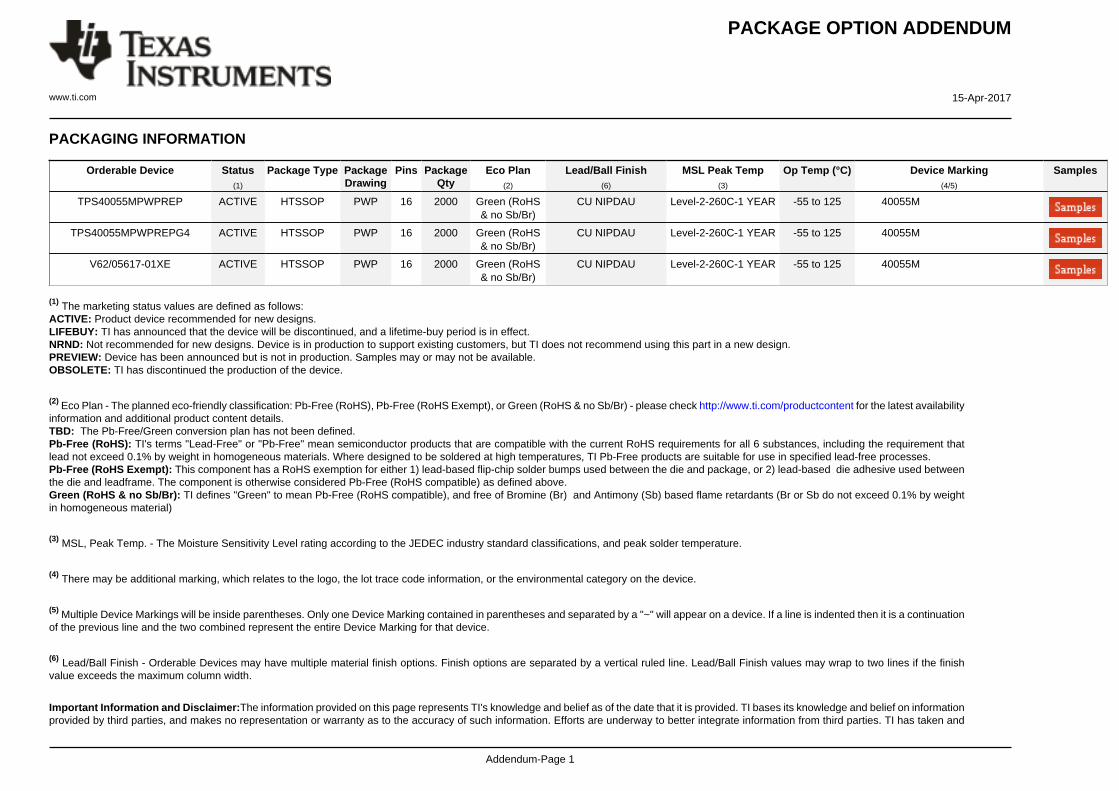
PACKAGING INFORMATION
Orderable Device Status(1)
Package Type PackageDrawing
Pins PackageQty
Eco Plan(2)
Lead/Ball Finish(6)
MSL Peak Temp(3)
Op Temp (°C) Device Marking(4/5)
Samples
TPS40055MPWPREP ACTIVE HTSSOP PWP 16 2000 Green (RoHS& no Sb/Br)
CU NIPDAU Level-2-260C-1 YEAR -55 to 125 40055M
TPS40055MPWPREPG4 ACTIVE HTSSOP PWP 16 2000 Green (RoHS& no Sb/Br)
CU NIPDAU Level-2-260C-1 YEAR -55 to 125 40055M
V62/05617-01XE ACTIVE HTSSOP PWP 16 2000 Green (RoHS& no Sb/Br)
CU NIPDAU Level-2-260C-1 YEAR -55 to 125 40055M
(1) The marketing status values are defined as follows:ACTIVE: Product device recommended for new designs.LIFEBUY: TI has announced that the device will be discontinued, and a lifetime-buy period is in effect.NRND: Not recommended for new designs. Device is in production to support existing customers, but TI does not recommend using this part in a new design.PREVIEW: Device has been announced but is not in production. Samples may or may not be available.OBSOLETE: TI has discontinued the production of the device.
(2) Eco Plan - The planned eco-friendly classification: Pb-Free (RoHS), Pb-Free (RoHS Exempt), or Green (RoHS & no Sb/Br) - please check http://www.ti.com/productcontent for the latest availabilityinformation and additional product content details.TBD: The Pb-Free/Green conversion plan has not been defined.Pb-Free (RoHS): TI's terms "Lead-Free" or "Pb-Free" mean semiconductor products that are compatible with the current RoHS requirements for all 6 substances, including the requirement thatlead not exceed 0.1% by weight in homogeneous materials. Where designed to be soldered at high temperatures, TI Pb-Free products are suitable for use in specified lead-free processes.Pb-Free (RoHS Exempt): This component has a RoHS exemption for either 1) lead-based flip-chip solder bumps used between the die and package, or 2) lead-based die adhesive used betweenthe die and leadframe. The component is otherwise considered Pb-Free (RoHS compatible) as defined above.Green (RoHS & no Sb/Br): TI defines "Green" to mean Pb-Free (RoHS compatible), and free of Bromine (Br) and Antimony (Sb) based flame retardants (Br or Sb do not exceed 0.1% by weightin homogeneous material)
(3) MSL, Peak Temp. - The Moisture Sensitivity Level rating according to the JEDEC industry standard classifications, and peak solder temperature.
(4) There may be additional marking, which relates to the logo, the lot trace code information, or the environmental category on the device.
(5) Multiple Device Markings will be inside parentheses. Only one Device Marking contained in parentheses and separated by a "~" will appear on a device. If a line is indented then it is a continuationof the previous line and the two combined represent the entire Device Marking for that device.
(6) Lead/Ball Finish - Orderable Devices may have multiple material finish options. Finish options are separated by a vertical ruled line. Lead/Ball Finish values may wrap to two lines if the finishvalue exceeds the maximum column width.
Important Information and Disclaimer:The information provided on this page represents TI's knowledge and belief as of the date that it is provided. TI bases its knowledge and belief on informationprovided by third parties, and makes no representation or warranty as to the accuracy of such information. Efforts are underway to better integrate information from third parties. TI has taken and

PACKAGE OPTION ADDENDUM
www.ti.com 15-Apr-2017
Addendum-Page 2
continues to take reasonable steps to provide representative and accurate information but may not have conducted destructive testing or chemical analysis on incoming materials and chemicals.TI and TI suppliers consider certain information to be proprietary, and thus CAS numbers and other limited information may not be available for release.
In no event shall TI's liability arising out of such information exceed the total purchase price of the TI part(s) at issue in this document sold by TI to Customer on an annual basis.
OTHER QUALIFIED VERSIONS OF TPS40055-EP :
• Catalog: TPS40055
NOTE: Qualified Version Definitions:
• Catalog - TI's standard catalog product

TAPE AND REEL INFORMATION
*All dimensions are nominal
Device PackageType
PackageDrawing
Pins SPQ ReelDiameter
(mm)
ReelWidth
W1 (mm)
A0(mm)
B0(mm)
K0(mm)
P1(mm)
W(mm)
Pin1Quadrant
TPS40055MPWPREP HTSSOP PWP 16 2000 330.0 12.4 6.9 5.6 1.6 8.0 12.0 Q1
PACKAGE MATERIALS INFORMATION
www.ti.com 17-Feb-2016
Pack Materials-Page 1

*All dimensions are nominal
Device Package Type Package Drawing Pins SPQ Length (mm) Width (mm) Height (mm)
TPS40055MPWPREP HTSSOP PWP 16 2000 367.0 367.0 38.0
PACKAGE MATERIALS INFORMATION
www.ti.com 17-Feb-2016
Pack Materials-Page 2


IMPORTANT NOTICE
Texas Instruments Incorporated (TI) reserves the right to make corrections, enhancements, improvements and other changes to itssemiconductor products and services per JESD46, latest issue, and to discontinue any product or service per JESD48, latest issue. Buyersshould obtain the latest relevant information before placing orders and should verify that such information is current and complete.TI’s published terms of sale for semiconductor products (http://www.ti.com/sc/docs/stdterms.htm) apply to the sale of packaged integratedcircuit products that TI has qualified and released to market. Additional terms may apply to the use or sale of other types of TI products andservices.Reproduction of significant portions of TI information in TI data sheets is permissible only if reproduction is without alteration and isaccompanied by all associated warranties, conditions, limitations, and notices. TI is not responsible or liable for such reproduceddocumentation. Information of third parties may be subject to additional restrictions. Resale of TI products or services with statementsdifferent from or beyond the parameters stated by TI for that product or service voids all express and any implied warranties for theassociated TI product or service and is an unfair and deceptive business practice. TI is not responsible or liable for any such statements.Buyers and others who are developing systems that incorporate TI products (collectively, “Designers”) understand and agree that Designersremain responsible for using their independent analysis, evaluation and judgment in designing their applications and that Designers havefull and exclusive responsibility to assure the safety of Designers' applications and compliance of their applications (and of all TI productsused in or for Designers’ applications) with all applicable regulations, laws and other applicable requirements. Designer represents that, withrespect to their applications, Designer has all the necessary expertise to create and implement safeguards that (1) anticipate dangerousconsequences of failures, (2) monitor failures and their consequences, and (3) lessen the likelihood of failures that might cause harm andtake appropriate actions. Designer agrees that prior to using or distributing any applications that include TI products, Designer willthoroughly test such applications and the functionality of such TI products as used in such applications.TI’s provision of technical, application or other design advice, quality characterization, reliability data or other services or information,including, but not limited to, reference designs and materials relating to evaluation modules, (collectively, “TI Resources”) are intended toassist designers who are developing applications that incorporate TI products; by downloading, accessing or using TI Resources in anyway, Designer (individually or, if Designer is acting on behalf of a company, Designer’s company) agrees to use any particular TI Resourcesolely for this purpose and subject to the terms of this Notice.TI’s provision of TI Resources does not expand or otherwise alter TI’s applicable published warranties or warranty disclaimers for TIproducts, and no additional obligations or liabilities arise from TI providing such TI Resources. TI reserves the right to make corrections,enhancements, improvements and other changes to its TI Resources. TI has not conducted any testing other than that specificallydescribed in the published documentation for a particular TI Resource.Designer is authorized to use, copy and modify any individual TI Resource only in connection with the development of applications thatinclude the TI product(s) identified in such TI Resource. NO OTHER LICENSE, EXPRESS OR IMPLIED, BY ESTOPPEL OR OTHERWISETO ANY OTHER TI INTELLECTUAL PROPERTY RIGHT, AND NO LICENSE TO ANY TECHNOLOGY OR INTELLECTUAL PROPERTYRIGHT OF TI OR ANY THIRD PARTY IS GRANTED HEREIN, including but not limited to any patent right, copyright, mask work right, orother intellectual property right relating to any combination, machine, or process in which TI products or services are used. Informationregarding or referencing third-party products or services does not constitute a license to use such products or services, or a warranty orendorsement thereof. Use of TI Resources may require a license from a third party under the patents or other intellectual property of thethird party, or a license from TI under the patents or other intellectual property of TI.TI RESOURCES ARE PROVIDED “AS IS” AND WITH ALL FAULTS. TI DISCLAIMS ALL OTHER WARRANTIES ORREPRESENTATIONS, EXPRESS OR IMPLIED, REGARDING RESOURCES OR USE THEREOF, INCLUDING BUT NOT LIMITED TOACCURACY OR COMPLETENESS, TITLE, ANY EPIDEMIC FAILURE WARRANTY AND ANY IMPLIED WARRANTIES OFMERCHANTABILITY, FITNESS FOR A PARTICULAR PURPOSE, AND NON-INFRINGEMENT OF ANY THIRD PARTY INTELLECTUALPROPERTY RIGHTS. TI SHALL NOT BE LIABLE FOR AND SHALL NOT DEFEND OR INDEMNIFY DESIGNER AGAINST ANY CLAIM,INCLUDING BUT NOT LIMITED TO ANY INFRINGEMENT CLAIM THAT RELATES TO OR IS BASED ON ANY COMBINATION OFPRODUCTS EVEN IF DESCRIBED IN TI RESOURCES OR OTHERWISE. IN NO EVENT SHALL TI BE LIABLE FOR ANY ACTUAL,DIRECT, SPECIAL, COLLATERAL, INDIRECT, PUNITIVE, INCIDENTAL, CONSEQUENTIAL OR EXEMPLARY DAMAGES INCONNECTION WITH OR ARISING OUT OF TI RESOURCES OR USE THEREOF, AND REGARDLESS OF WHETHER TI HAS BEENADVISED OF THE POSSIBILITY OF SUCH DAMAGES.Unless TI has explicitly designated an individual product as meeting the requirements of a particular industry standard (e.g., ISO/TS 16949and ISO 26262), TI is not responsible for any failure to meet such industry standard requirements.Where TI specifically promotes products as facilitating functional safety or as compliant with industry functional safety standards, suchproducts are intended to help enable customers to design and create their own applications that meet applicable functional safety standardsand requirements. Using products in an application does not by itself establish any safety features in the application. Designers mustensure compliance with safety-related requirements and standards applicable to their applications. Designer may not use any TI products inlife-critical medical equipment unless authorized officers of the parties have executed a special contract specifically governing such use.Life-critical medical equipment is medical equipment where failure of such equipment would cause serious bodily injury or death (e.g., lifesupport, pacemakers, defibrillators, heart pumps, neurostimulators, and implantables). Such equipment includes, without limitation, allmedical devices identified by the U.S. Food and Drug Administration as Class III devices and equivalent classifications outside the U.S.TI may expressly designate certain products as completing a particular qualification (e.g., Q100, Military Grade, or Enhanced Product).Designers agree that it has the necessary expertise to select the product with the appropriate qualification designation for their applicationsand that proper product selection is at Designers’ own risk. Designers are solely responsible for compliance with all legal and regulatoryrequirements in connection with such selection.Designer will fully indemnify TI and its representatives against any damages, costs, losses, and/or liabilities arising out of Designer’s non-compliance with the terms and provisions of this Notice.
Mailing Address: Texas Instruments, Post Office Box 655303, Dallas, Texas 75265Copyright © 2017, Texas Instruments Incorporated