service manuals lg tv lcd 42lg61yd 42lg61yd service manual
DESCRIPTION
LG LCDTRANSCRIPT

LCD TVSERVICE MANUAL
CAUTIONBEFORE SERVICING THE CHASSIS,READ THE SAFETY PRECAUTIONS IN THIS MANUAL.
CHASSIS : LB81C
MODEL : 42LG61YD 42LG61YD-AC
website:http://biz.LGservice.comInternal Use Only

LGE Internal Use OnlyCopyright © 2008 LG Electronics. Inc. All right reserved. Only for training and service purposes
- 2 -
CONTENTS
CONTENTS .............................................................................................. 2
PRODUCT SAFETY ..................................................................................3
SPECIFICATION ........................................................................................6
ADJUSTMENT INSTRUCTION ...............................................................12
TROUBLE SHOOTING ............................................................................18
BLOCK DIAGRAM...................................................................................22
EXPLODED VIEW .................................................................................. 34
SVC. SHEET ...............................................................................................
LGE Internal Use OnlyCopyright © 2008 LG Electronics. Inc. All right reserved. Only for training and service purposes
- 3 -
SAFETY PRECAUTIONS
Many electrical and mechanical parts in this chassis have special safety-related characteristics. These parts are identified by in theSchematic Diagram and Replacement Parts List. It is essential that these special safety parts should be replaced with the same components as recommended in this manual to preventShock, Fire, or other Hazards. Do not modify the original design without permission of manufacturer.
General Guidance
An isolation Transformer should always be used during theservicing of a receiver whose chassis is not isolated from the ACpower line. Use a transformer of adequate power rating as thisprotects the technician from accidents resulting in personal injuryfrom electrical shocks.
It will also protect the receiver and it's components from beingdamaged by accidental shorts of the circuitry that may beinadvertently introduced during the service operation.
If any fuse (or Fusible Resistor) in this TV receiver is blown,replace it with the specified.
When replacing a high wattage resistor (Oxide Metal Film Resistor,over 1W), keep the resistor 10mm away from PCB.
Keep wires away from high voltage or high temperature parts.
Before returning the receiver to the customer,
always perform an AC leakage current check on the exposedmetallic parts of the cabinet, such as antennas, terminals, etc., tobe sure the set is safe to operate without damage of electricalshock.
Leakage Current Cold Check(Antenna Cold Check)With the instrument AC plug removed from AC source, connect anelectrical jumper across the two AC plug prongs. Place the ACswitch in the on position, connect one lead of ohm-meter to the ACplug prongs tied together and touch other ohm-meter lead in turn toeach exposed metallic parts such as antenna terminals, phonejacks, etc. If the exposed metallic part has a return path to the chassis, themeasured resistance should be between 1MΩ and 5.2MΩ. When the exposed metal has no return path to the chassis thereading must be infinite.An other abnormality exists that must be corrected before thereceiver is returned to the customer.
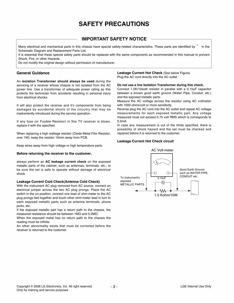
Leakage Current Hot Check (See below Figure) Plug the AC cord directly into the AC outlet.
Do not use a line Isolation Transformer during this check.Connect 1.5K/10watt resistor in parallel with a 0.15uF capacitorbetween a known good earth ground (Water Pipe, Conduit, etc.)and the exposed metallic parts.Measure the AC voltage across the resistor using AC voltmeterwith 1000 ohms/volt or more sensitivity.Reverse plug the AC cord into the AC outlet and repeat AC voltagemeasurements for each exposed metallic part. Any voltagemeasured must not exceed 0.75 volt RMS which is corresponds to0.5mA.In case any measurement is out of the limits specified, there ispossibility of shock hazard and the set must be checked andrepaired before it is returned to the customer.
Leakage Current Hot Check circuit
1.5 Kohm/10W
To Instrument'sexposed METALLIC PARTS
Good Earth Groundsuch as WATER PIPE,CONDUIT etc.
AC Volt-meter
IMPORTANT SAFETY NOTICE
0.15uF
LGE Internal Use OnlyCopyright © 2008 LG Electronics. Inc. All right reserved. Only for training and service purposes
- 4 -
CAUTION: Before servicing receivers covered by this servicemanual and its supplements and addenda, read and follow theSAFETY PRECAUTIONS on page 3 of this publication.NOTE: If unforeseen circumstances create conflict between thefollowing servicing precautions and any of the safety precautions onpage 3 of this publication, always follow the safety precautions.Remember: Safety First.
General Servicing Precautions1. Always unplug the receiver AC power cord from the AC power
source before;a. Removing or reinstalling any component, circuit board
module or any other receiver assembly.b. Disconnecting or reconnecting any receiver electrical plug or
other electrical connection.c. Connecting a test substitute in parallel with an electrolytic
capacitor in the receiver.CAUTION: A wrong part substitution or incorrect polarityinstallation of electrolytic capacitors may result in anexplosion hazard.
2. Test high voltage only by measuring it with an appropriate highvoltage meter or other voltage measuring device (DVM,FETVOM, etc) equipped with a suitable high voltage probe.Do not test high voltage by "drawing an arc".
3. Do not spray chemicals on or near this receiver or any of itsassemblies.
4. Unless specified otherwise in this service manual, cleanelectrical contacts only by applying the following mixture to thecontacts with a pipe cleaner, cotton-tipped stick or comparablenon-abrasive applicator; 10% (by volume) Acetone and 90% (byvolume) isopropyl alcohol (90%-99% strength)CAUTION: This is a flammable mixture.Unless specified otherwise in this service manual, lubrication ofcontacts in not required.
5. Do not defeat any plug/socket B+ voltage interlocks with whichreceivers covered by this service manual might be equipped.
6. Do not apply AC power to this instrument and/or any of itselectrical assemblies unless all solid-state device heat sinks arecorrectly installed.
7. Always connect the test receiver ground lead to the receiverchassis ground before connecting the test receiver positivelead.Always remove the test receiver ground lead last.
8. Use with this receiver only the test fixtures specified in thisservice manual.CAUTION: Do not connect the test fixture ground strap to anyheat sink in this receiver.
Electrostatically Sensitive (ES) DevicesSome semiconductor (solid-state) devices can be damaged easilyby static electricity. Such components commonly are calledElectrostatically Sensitive (ES) Devices. Examples of typical ESdevices are integrated circuits and some field-effect transistors andsemiconductor "chip" components. The following techniquesshould be used to help reduce the incidence of componentdamage caused by static by static electricity.1. Immediately before handling any semiconductor component or
semiconductor-equipped assembly, drain off any electrostaticcharge on your body by touching a known earth ground.Alternatively, obtain and wear a commercially availabledischarging wrist strap device, which should be removed toprevent potential shock reasons prior to applying power to the
unit under test.2. After removing an electrical assembly equipped with ES
devices, place the assembly on a conductive surface such asaluminum foil, to prevent electrostatic charge buildup orexposure of the assembly.
3. Use only a grounded-tip soldering iron to solder or unsolder ESdevices.
4. Use only an anti-static type solder removal device. Some solderremoval devices not classified as "anti-static" can generateelectrical charges sufficient to damage ES devices.
5. Do not use freon-propelled chemicals. These can generateelectrical charges sufficient to damage ES devices.
6. Do not remove a replacement ES device from its protectivepackage until immediately before you are ready to install it.(Most replacement ES devices are packaged with leadselectrically shorted together by conductive foam, aluminum foilor comparable conductive material).
7. Immediately before removing the protective material from theleads of a replacement ES device, touch the protective materialto the chassis or circuit assembly into which the device will beinstalled.CAUTION: Be sure no power is applied to the chassis or circuit,and observe all other safety precautions.
8. Minimize bodily motions when handling unpackagedreplacement ES devices. (Otherwise harmless motion such asthe brushing together of your clothes fabric or the lifting of yourfoot from a carpeted floor can generate static electricitysufficient to damage an ES device.)
General Soldering Guidelines1. Use a grounded-tip, low-wattage soldering iron and appropriate
tip size and shape that will maintain tip temperature within therange or 500°F to 600°F.
2. Use an appropriate gauge of RMA resin-core solder composedof 60 parts tin/40 parts lead.
3. Keep the soldering iron tip clean and well tinned.4. Thoroughly clean the surfaces to be soldered. Use a mall wire-
bristle (0.5 inch, or 1.25cm) brush with a metal handle.Do not use freon-propelled spray-on cleaners.
5. Use the following unsoldering techniquea. Allow the soldering iron tip to reach normal temperature.
(500°F to 600°F)b. Heat the component lead until the solder melts.c. Quickly draw the melted solder with an anti-static, suction-
type solder removal device or with solder braid.CAUTION: Work quickly to avoid overheating the circuitboard printed foil.
6. Use the following soldering technique.a. Allow the soldering iron tip to reach a normal temperature
(500°F to 600°F)b. First, hold the soldering iron tip and solder the strand against
the component lead until the solder melts.c. Quickly move the soldering iron tip to the junction of the
component lead and the printed circuit foil, and hold it thereonly until the solder flows onto and around both thecomponent lead and the foil.CAUTION: Work quickly to avoid overheating the circuitboard printed foil.
d. Closely inspect the solder area and remove any excess orsplashed solder with a small wire-bristle brush.
SERVICING PRECAUTIONS

LGE Internal Use OnlyCopyright © 2008 LG Electronics. Inc. All right reserved. Only for training and service purposes
- 5 -
IC Remove/ReplacementSome chassis circuit boards have slotted holes (oblong) throughwhich the IC leads are inserted and then bent flat against thecircuit foil. When holes are the slotted type, the following techniqueshould be used to remove and replace the IC. When working withboards using the familiar round hole, use the standard techniqueas outlined in paragraphs 5 and 6 above.
Removal1. Desolder and straighten each IC lead in one operation by gently
prying up on the lead with the soldering iron tip as the soldermelts.
2. Draw away the melted solder with an anti-static suction-typesolder removal device (or with solder braid) before removing theIC.
Replacement1. Carefully insert the replacement IC in the circuit board.2. Carefully bend each IC lead against the circuit foil pad and
solder it.3. Clean the soldered areas with a small wire-bristle brush.
(It is not necessary to reapply acrylic coating to the areas).
"Small-Signal" Discrete TransistorRemoval/Replacement1. Remove the defective transistor by clipping its leads as close as
possible to the component body.2. Bend into a "U" shape the end of each of three leads remaining
on the circuit board.3. Bend into a "U" shape the replacement transistor leads.4. Connect the replacement transistor leads to the corresponding
leads extending from the circuit board and crimp the "U" withlong nose pliers to insure metal to metal contact then soldereach connection.
Power Output, Transistor DeviceRemoval/Replacement1. Heat and remove all solder from around the transistor leads.2. Remove the heat sink mounting screw (if so equipped).3. Carefully remove the transistor from the heat sink of the circuit
board.4. Insert new transistor in the circuit board.5. Solder each transistor lead, and clip off excess lead.6. Replace heat sink.
Diode Removal/Replacement1. Remove defective diode by clipping its leads as close as
possible to diode body.2. Bend the two remaining leads perpendicular y to the circuit
board.3. Observing diode polarity, wrap each lead of the new diode
around the corresponding lead on the circuit board.4. Securely crimp each connection and solder it.5. Inspect (on the circuit board copper side) the solder joints of
the two "original" leads. If they are not shiny, reheat them and ifnecessary, apply additional solder.
Fuse and Conventional ResistorRemoval/Replacement1. Clip each fuse or resistor lead at top of the circuit board hollow
stake.2. Securely crimp the leads of replacement component around
notch at stake top.3. Solder the connections.
CAUTION: Maintain original spacing between the replacedcomponent and adjacent components and the circuit board toprevent excessive component temperatures.
Circuit Board Foil RepairExcessive heat applied to the copper foil of any printed circuitboard will weaken the adhesive that bonds the foil to the circuitboard causing the foil to separate from or "lift-off" the board. Thefollowing guidelines and procedures should be followed wheneverthis condition is encountered.
At IC ConnectionsTo repair a defective copper pattern at IC connections use thefollowing procedure to install a jumper wire on the copper patternside of the circuit board. (Use this technique only on ICconnections).
1. Carefully remove the damaged copper pattern with a sharpknife. (Remove only as much copper as absolutely necessary).
2. carefully scratch away the solder resist and acrylic coating (ifused) from the end of the remaining copper pattern.
3. Bend a small "U" in one end of a small gauge jumper wire andcarefully crimp it around the IC pin. Solder the IC connection.
4. Route the jumper wire along the path of the out-away copperpattern and let it overlap the previously scraped end of the goodcopper pattern. Solder the overlapped area and clip off anyexcess jumper wire.
At Other ConnectionsUse the following technique to repair the defective copper patternat connections other than IC Pins. This technique involves theinstallation of a jumper wire on the component side of the circuitboard.
1. Remove the defective copper pattern with a sharp knife.Remove at least 1/4 inch of copper, to ensure that a hazardouscondition will not exist if the jumper wire opens.
2. Trace along the copper pattern from both sides of the patternbreak and locate the nearest component that is directlyconnected to the affected copper pattern.
3. Connect insulated 20-gauge jumper wire from the lead of thenearest component on one side of the pattern break to the leadof the nearest component on the other side.Carefully crimp and solder the connections.CAUTION: Be sure the insulated jumper wire is dressed so theit does not touch components or sharp edges.
LGE Internal Use OnlyCopyright © 2008 LG Electronics. Inc. All right reserved. Only for training and service purposes
- 6 -
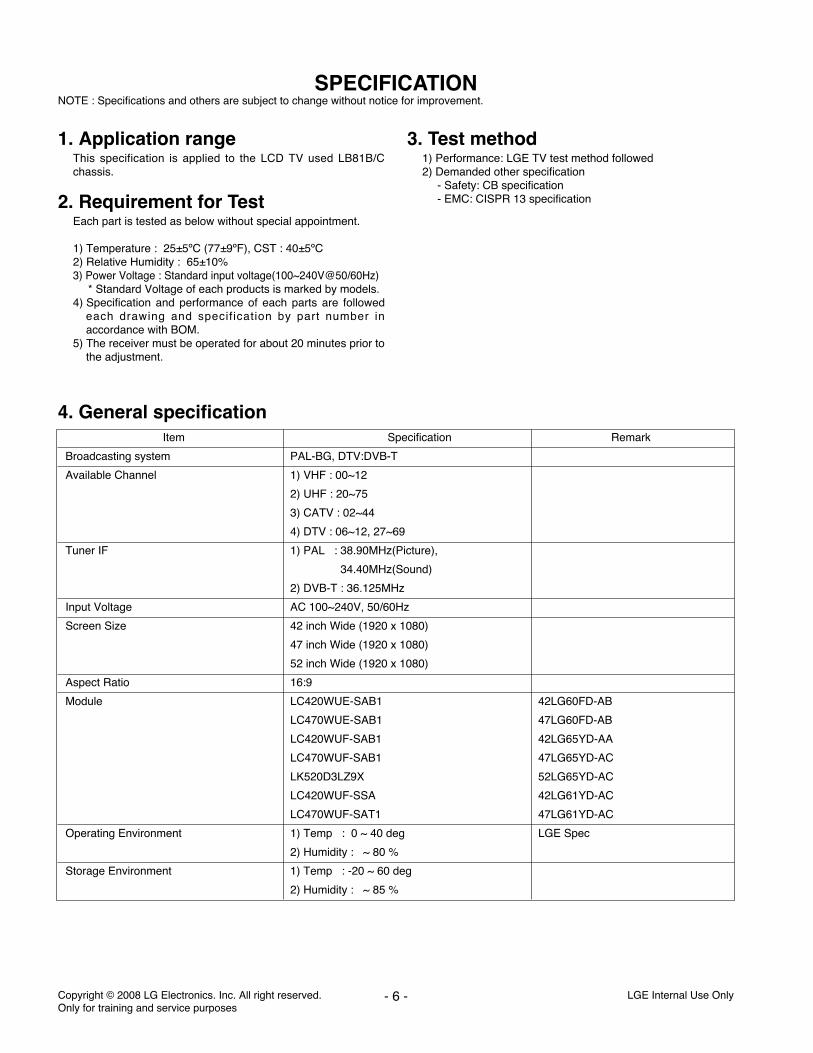
SPECIFICATIONNOTE : Specifications and others are subject to change without notice for improvement.
4. General specificationItem Specification Remark
Broadcasting system PAL-BG, DTV:DVB-T
Available Channel 1) VHF : 00~12
2) UHF : 20~75
3) CATV : 02~44
4) DTV : 06~12, 27~69
Tuner IF 1) PAL : 38.90MHz(Picture),
34.40MHz(Sound)
2) DVB-T : 36.125MHz
Input Voltage AC 100~240V, 50/60Hz
Screen Size 42 inch Wide (1920 x 1080)
47 inch Wide (1920 x 1080)
52 inch Wide (1920 x 1080)
Aspect Ratio 16:9
Module LC420WUE-SAB1 42LG60FD-AB
LC470WUE-SAB1 47LG60FD-AB
LC420WUF-SAB1 42LG65YD-AA
LC470WUF-SAB1 47LG65YD-AC
LK520D3LZ9X 52LG65YD-AC
LC420WUF-SSA 42LG61YD-AC
LC470WUF-SAT1 47LG61YD-AC
Operating Environment 1) Temp : 0 ~ 40 deg LGE Spec
2) Humidity : ~ 80 %
Storage Environment 1) Temp : -20 ~ 60 deg
2) Humidity : ~ 85 %
1. Application rangeThis specification is applied to the LCD TV used LB81B/Cchassis.
2. Requirement for TestEach part is tested as below without special appointment.
1) Temperature : 25±5ºC (77±9ºF), CST : 40±5ºC2) Relative Humidity : 65±10%3) Power Voltage : Standard input voltage(100~240V@50/60Hz)
* Standard Voltage of each products is marked by models.4) Specification and performance of each parts are followed
each drawing and specif ication by part number inaccordance with BOM.
5) The receiver must be operated for about 20 minutes prior tothe adjustment.
3. Test method1) Performance: LGE TV test method followed 2) Demanded other specification
- Safety: CB specification- EMC: CISPR 13 specification
- 7 - LGE Internal Use OnlyCopyright © 2008 LG Electronics. Inc. All right reserved. Only for training and service purposes
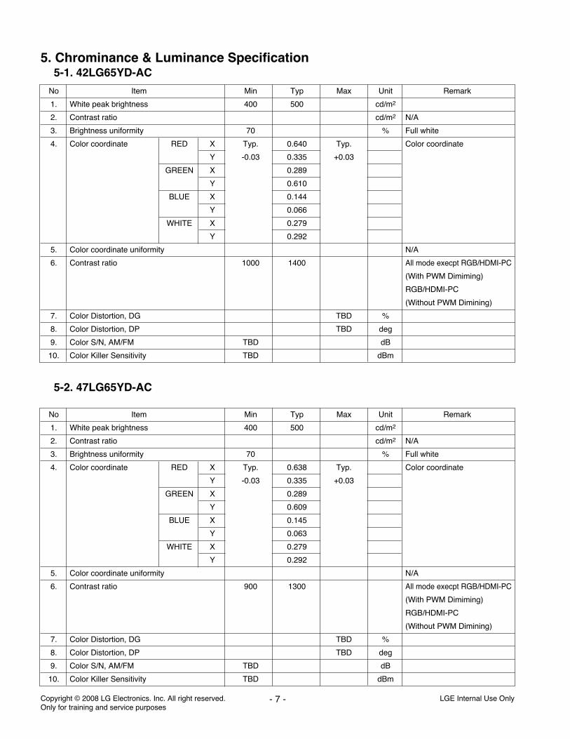
5. Chrominance & Luminance Specification5-1. 42LG65YD-AC
5-2. 47LG65YD-AC
No Item Min Typ Max Unit Remark
1. White peak brightness 400 500 cd/m2
2. Contrast ratio cd/m2 N/A
3. Brightness uniformity 70 % Full white
4. Color coordinate RED X Typ. 0.640 Typ. Color coordinate
Y -0.03 0.335 +0.03
GREEN X 0.289
Y 0.610
BLUE X 0.144
Y 0.066
WHITE X 0.279
Y 0.292
5. Color coordinate uniformity N/A
6. Contrast ratio 1000 1400 All mode execpt RGB/HDMI-PC
(With PWM Dimiming)
RGB/HDMI-PC
(Without PWM Dimining)
7. Color Distortion, DG TBD %
8. Color Distortion, DP TBD deg
9. Color S/N, AM/FM TBD dB
10. Color Killer Sensitivity TBD dBm
No Item Min Typ Max Unit Remark
1. White peak brightness 400 500 cd/m2
2. Contrast ratio cd/m2 N/A
3. Brightness uniformity 70 % Full white
4. Color coordinate RED X Typ. 0.638 Typ. Color coordinate
Y -0.03 0.335 +0.03
GREEN X 0.289
Y 0.609
BLUE X 0.145
Y 0.063
WHITE X 0.279
Y 0.292
5. Color coordinate uniformity N/A
6. Contrast ratio 900 1300 All mode execpt RGB/HDMI-PC
(With PWM Dimiming)
RGB/HDMI-PC
(Without PWM Dimining)
7. Color Distortion, DG TBD %
8. Color Distortion, DP TBD deg
9. Color S/N, AM/FM TBD dB
10. Color Killer Sensitivity TBD dBm
- 8 - LGE Internal Use OnlyCopyright © 2008 LG Electronics. Inc. All right reserved. Only for training and service purposes
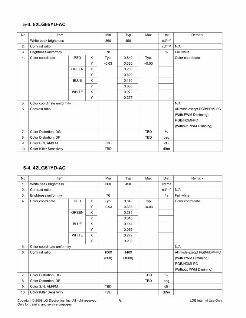
5-3. 52LG65YD-AC
No Item Min Typ Max Unit Remark
1. White peak brightness 360 450 cd/m2
2. Contrast ratio cd/m2 N/A
3. Brightness uniformity 70 % Full white
4. Color coordinate RED X Typ. 0.640 Typ. Color coordinate
Y -0.03 0.330 +0.03
GREEN X 0.280
Y 0.600
BLUE X 0.150
Y 0.060
WHITE X 0.272
Y 0.277
5. Color coordinate uniformity N/A
6. Contrast ratio All mode execpt RGB/HDMI-PC
(With PWM Dimiming)
RGB/HDMI-PC
(Without PWM Dimining)
7. Color Distortion, DG TBD %
8. Color Distortion, DP TBD deg
9. Color S/N, AM/FM TBD dB
10. Color Killer Sensitivity TBD dBm
5-4. 42LG61YD-AC
No Item Min Typ Max Unit Remark
1. White peak brightness 360 450 cd/m2
2. Contrast ratio cd/m2 N/A
3. Brightness uniformity 70 % Full white
4. Color coordinate RED X Typ. 0.640 Typ. Color coordinate
Y -0.03 0.335 +0.03
GREEN X 0.289
Y 0.610
BLUE X 0.144
Y 0.066
WHITE X 0.279
Y 0.292
5. Color coordinate uniformity N/A
6. Contrast ratio 1000 1400 All mode execpt RGB/HDMI-PC
(800) (1000) (With PWM Dimiming)
RGB/HDMI-PC
(Without PWM Dimining)
7. Color Distortion, DG TBD %
8. Color Distortion, DP TBD deg
9. Color S/N, AM/FM TBD dB
10. Color Killer Sensitivity TBD dBm

- 9 - LGE Internal Use OnlyCopyright © 2008 LG Electronics. Inc. All right reserved. Only for training and service purposes
5-5. 47LG61YD-AC
No Item Min Typ Max Unit Remark
1. White peak brightness 360 450 cd/m2
2. Contrast ratio cd/m2 N/A
3. Brightness uniformity 70 % Full white
4. Color coordinate RED X Typ. 0.638 Typ. Color coordinate
Y -0.03 0.335 +0.03
GREEN X 0.289
Y 0.610
BLUE X 0.145
Y 0.063
WHITE X 0.279
Y 0.292
5. Color coordinate uniformity N/A
6. Contrast ratio 900 1300 All mode execpt RGB/HDMI-PC
(With PWM Dimiming)
RGB/HDMI-PC
(Without PWM Dimining)
7. Color Distortion, DG TBD %
8. Color Distortion, DP TBD deg
9. Color S/N, AM/FM TBD dB
10. Color Killer Sensitivity TBD dBm
LGE Internal Use OnlyCopyright © 2008 LG Electronics. Inc. All right reserved. Only for training and service purposes
- 10 -
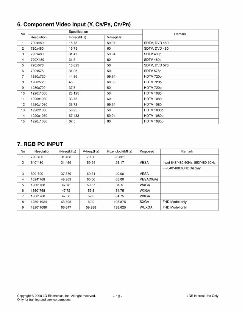
7. RGB PC INPUTNo Resolution H-freq(kHz) V-freq.(Hz) Pixel clock(MHz) Proposed Remark
1 720*400 31.468 70.08 28.321
2 640*480 31.469 59.94 25.17 VESA Input 848*480 60Hz, 852*480 60Hz
=> 640*480 60Hz Display
3 800*600 37.879 60.31 40.00 VESA
4 1024*768 48.363 60.00 65.00 VESA(XGA)
5 1280*768 47.78 59.87 79.5 WXGA
6 1360*768 47.72 59.8 84.75 WXGA
7 1366*768 47.56 59.6 84.75 WXGA
8 1280*1024 63.595 60.0 108.875 SXGA FHD Model only
9 1920*1080 66.647 59.988 138.625 WUXGA FHD Model only
6. Component Video Input (Y, CB/PB, CR/PR)
NoSpecification
RemarkResolution H-freq(kHz) V-freq(Hz)
1 720x480 15.73 59.94 SDTV, DVD 480i
2 720x480 15.75 60 SDTV, DVD 480i
3 720x480 31.47 59.94 SDTV 480p
4 720X480 31.5 60 SDTV 480p
5 720x576 15.625 50 SDTV, DVD 576i
6 720x576 31.25 50 SDTV 576p
7 1280x720 44.96 59.94 HDTV 720p
8 1280x720 45 60.36 HDTV 720p
9 1280x720 37.5 50 HDTV 720p
10 1920x1080 28.125 50 HDTV 1080i
11 1920x1080 33.75 60 HDTV 1080i
12 1920x1080 33.72 59.94 HDTV 1080i
13 1920x1080 56.25 50 HDTV 1080p
14 1920x1080 67.433 59.94 HDTV 1080p
15 1920x1080 67.5 60 HDTV 1080p
LGE Internal Use OnlyCopyright © 2008 LG Electronics. Inc. All right reserved. Only for training and service purposes
- 11 -
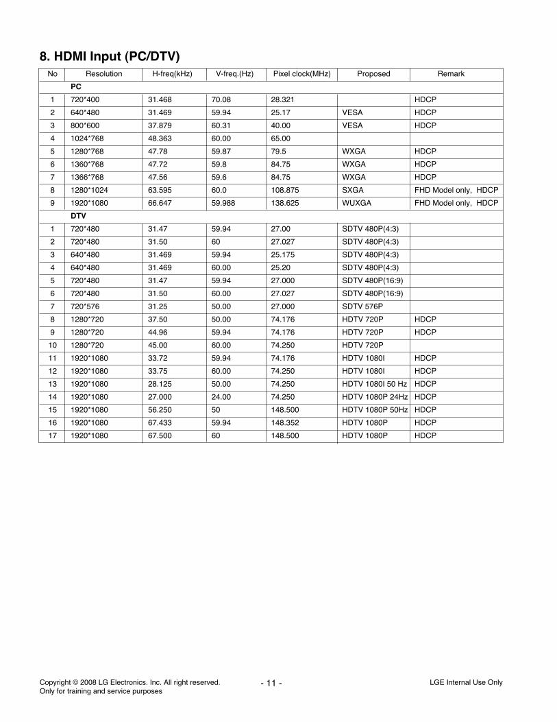
8. HDMI Input (PC/DTV)No Resolution H-freq(kHz) V-freq.(Hz) Pixel clock(MHz) Proposed Remark
PC
1 720*400 31.468 70.08 28.321 HDCP
2 640*480 31.469 59.94 25.17 VESA HDCP
3 800*600 37.879 60.31 40.00 VESA HDCP
4 1024*768 48.363 60.00 65.00
5 1280*768 47.78 59.87 79.5 WXGA HDCP
6 1360*768 47.72 59.8 84.75 WXGA HDCP
7 1366*768 47.56 59.6 84.75 WXGA HDCP
8 1280*1024 63.595 60.0 108.875 SXGA FHD Model only, HDCP
9 1920*1080 66.647 59.988 138.625 WUXGA FHD Model only, HDCP
DTV
1 720*480 31.47 59.94 27.00 SDTV 480P(4:3)
2 720*480 31.50 60 27.027 SDTV 480P(4:3)
3 640*480 31.469 59.94 25.175 SDTV 480P(4:3)
4 640*480 31.469 60.00 25.20 SDTV 480P(4:3)
5 720*480 31.47 59.94 27.000 SDTV 480P(16:9)
6 720*480 31.50 60.00 27.027 SDTV 480P(16:9)
7 720*576 31.25 50.00 27.000 SDTV 576P
8 1280*720 37.50 50.00 74.176 HDTV 720P HDCP
9 1280*720 44.96 59.94 74.176 HDTV 720P HDCP
10 1280*720 45.00 60.00 74.250 HDTV 720P
11 1920*1080 33.72 59.94 74.176 HDTV 1080I HDCP
12 1920*1080 33.75 60.00 74.250 HDTV 1080I HDCP
13 1920*1080 28.125 50.00 74.250 HDTV 1080I 50 Hz HDCP
14 1920*1080 27.000 24.00 74.250 HDTV 1080P 24Hz HDCP
15 1920*1080 56.250 50 148.500 HDTV 1080P 50Hz HDCP
16 1920*1080 67.433 59.94 148.352 HDTV 1080P HDCP
17 1920*1080 67.500 60 148.500 HDTV 1080P HDCP

LGE Internal Use OnlyCopyright © 2008 LG Electronics. Inc. All right reserved. Only for training and service purposes
- 12 -
ADJUSTMENT INSTRUCTION
1. Application RangeThis specification sheet is applied to all of the LCD TV withLB81C chassis.
2. Designation1) The adjustment is according to the order which is
designated and which must be followed, according to theplan which can be changed only on agreeing.
2) Power Adjustment: Free Voltage3) Magnetic Field Condition: Nil.4) Input signal Unit: Product Specification Standard5) Reserve after operation: Above 5 Minutes (Heat Run)
Temperature : at 25±5ºC Relative humidity : 65±10%Input voltage : 220V, 60Hz
6) Adjustment equipments: Color Analyzer (CA-210 or CA-110), Pattern Generator (MSPG-925L or Equivalent), DDCAdjustment Jig equipment, SVC remote controller
7) Don’t push The “IN STOP KEY” after completing thefunction inspection.
3. Main PCB check process* APC - After Manual-Insult, executing APC
* Download 1) Execute ISP program “Mstar ISP Utility” and then click
“Config” tab.2) Set as below, and then click “Auto Detect” and check “OK”
message. If display “Error”, Check connect computer, jig,and set.
3) Click “Connect” tab. If display “Can’t”, Check connectcomputer, jig, and set.
4) Click “Read” tab, and then load download file(XXXX.bin) byclicking “Read”.
5. Click “Auto” tab and set as below6. Click “Run”.7. After downloading, check “OK” message.
* USB DOWNLOAD1) Put the USB Stick to the USB socket
2) Automatically detecting update file in USB Stick- If your downloaded program version in USB Stick is Low,
it didn’t work. But your downloaded version is High, USBdata is automatically detecting
3) Show the message “Copying files from memory”
4) Updating is staring.
5) Fishing the version uploading, you have to put USB stickand “AC Power” off.
6) After putting “AC Power” on and check updated version onyour TV.
USB
(1) (3)
(2) OK
Please Check Speed :To us speed between from 200 KHzto 400 KHz
(4)
filexxx.bin
(5)
(7) ........ OK
(6)
filexxx.bin
LGE Internal Use OnlyCopyright © 2008 LG Electronics. Inc. All right reserved. Only for training and service purposes
- 13 -
* After downloading, have to adjust Tool Option again.1) Push "IN-START" key in service remote controller 2) Select "MODEL SELECT" and Push “OK” button.3) Go To “INCH” and choice proper inch.4) TV power turn off and on.5) Completed selecting Tool option
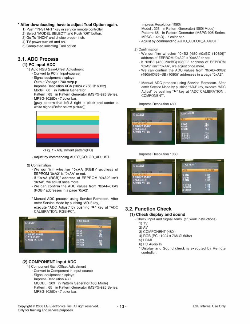
3.1. ADC Process (1) PC input ADC
1) Auto RGB Gain/Offset Adjustment- Convert to PC in Input-source- Signal equipment displays
Output Voltage : 700 mVp-pImpress Resolution XGA (1024 x 768 @ 60Hz) Model : 60 in Pattern GeneratorPattern : 65 in Pattern Generator (MSPG-925 Series,MPSG-1025D) - 7 color bar.[gray pattern that left & right is black and center iswhite signal(Refer below picture)]
- Adjust by commanding AUTO_COLOR_ADJUST.
2) Confirmation- We confirm whether “0xAA (RGB)” address of
EEPROM “0xA2” is “0xAA” or not. - If “0xAA (RGB)” address of EEPROM “0xA2” isn’t
“0xAA”, we adjust once more- We can confirm the ADC values from “0xA4~0XA9
(RGB)” addresses in a page “0xA2”
* Manual ADC process using Service Remocon. Afterenter Service Mode by pushing “ADJ” key,execute “ADC Adjust” by pushing “G” key at “ADCCALIBRATION: RGB-PC”.
(2) COMPONENT input ADC 1) Component Gain/Offset Adjustment
- Convert to Component in Input-source- Signal equipment displays
Impress Resolution 480iMODEL : 209 in Pattern Generator(480i Mode)Pattern : 65 in Pattern Generator (MSPG-925 Series,MPSG-1025D) - 7 color bar.
Impress Resolution 1080iModel : 223 in Pattern Generator(1080i Mode)Pattern: 65 in Pattern Generator (MSPG-925 Series,MPSG-1025D) - 7 color bar.
- Adjust by commanding AUTO_COLOR_ADJUST.
2) Confirmation- We confirm whether “0xB3 (480i)/0xBC (1080i)”
address of EEPROM “0xA2” is “0xAA” or not.- If “0xB3 (480i)/0xBC(1080i)” address of EEPROM
“0xA2” isn’t “0xAA”, we adjust once more.- We can confirm the ADC values from “0xAD~0XB2
(480i)/0XB6~BB (1080i)” addresses in a page “0xA2”.
* Manual ADC process using Service Remocon. Afterenter Service Mode by pushing “ADJ” key, execute “ADCAdjust” by pushing “G” key at “ADC CALIBRATION :COMPONENT”.
Impress Resolution 480i
Impress Resolution 1080i
3.2. Function Check(1) Check display and sound
- Check Input and Signal items. (cf. work instructions) 1) TV2) AV 3) COMPONENT (480i)4) RGB (PC : 1024 x 768 @ 60hz)5) HDMI6) PC Audio In * Display and Sound check is executed by Remote
controller.
<Fig. 1> Adjustment pattern(PC)

4. Total Assembly line process4.1. Adjustment Preparation
(1) W/B Equipment conditionCA210: CH 9, Test signal: Inner pattern (85IRE)
(2) Above 5 minutes H/run in the inner pattern. (“power on”key of adjust remote control)
(3) 15 Pin D-Sub Jack is connected to the AUTO W/BEQUIPMENT.
(4) Adjust Process will start by execute I2C Command (Innerpattern (0xF3, 0xFF).
(5) Adjust Process will finish by execute I2C Command (Innerpattern (Inner pattern (0xF3,0x00)).
** Caution ** Color Temperature: COOL, Medium, WarmOne of R Gain/G Gain/ B Gain should be kept on 0xC0, andadjust other two lower than C0.(when R/G/B Gain are all C0, it is the FULL Dynamic Rangeof Module)
* Manual W/B process using adjusts Remote control. - After enter Service Mode by pushing “ADJ” key,- Enter White Pattern off of service mode, and change off
---> on.- Enter “W/B ADJUST” by pushing “G” key at “3.W/B
ADJUST”.- The default value of RGB-GAIN is 192 at cool, Medium,
Warm(There is a difference between picture image and set)
* After done all adjustments, Press “In-start” button andcompare Tool option and Area option value with its BOM, if itis correctly same then unplug the AC cable.If it is not same, then correct it same with BOM and unplugAC cable.For correct it to the model’s module from factory JIG model.
* Don’t push The “IN STOP KEY” after completing the functioninspection.
4.2. DPM operation confirmation(Only Apply for MNT Model)
Check if Power LED Color and Power Consumption operateas standard. - Set Input to RGB and connect D-sub cable to set- Measurement Condition: (100-240V@ 50/60Hz)- Confirm DPM operation at the state of screen without Signal
4.3. DDC EDID Write (RGB 128Byte)- Connect D-sub signal cable to D-sub Jack.- Write EDID Data to EEPROM(24C02) by using DDC2B
protocol.- Check whether written EDID data is correct or not.
4.4. DDC EDID Write (HDMI 256Byte) In case of 2008 year new model for Australia and Taiwanwhich is developed with Mstar scaler, Manufacture gave nouse for downlad of EDID for HDMI 1/2/3/4 because HDMIEDID data is in the Application Program.
4.5. LB81C EDID Data (42LG60FD-AA, 47LG60FD-AA, 42LG65YD-AC, 47LG65YD-AA. 52LG65YD-AA, 42LG61YD-AC, 47LG61YD-AC)No USE the EDID data of Digital data(HDMI 1, 2, 3, 4) andAnalog EDID data (RGB) As EDID data is recorded in theMstar (Main IC).
4.5.1 Analog data 128Byte(2Bi) - Not USE
EDID block 0, Bytes 0-127[00H-7FH]Block Type : EDID 1.3
4.5.2 Digital data(HDMI-1) 256Byte
EDID block 0, Bytes 0-127[00H-7FH]Block Type : EDID 1.3
- 14 - LGE Internal Use OnlyCopyright © 2008 LG Electronics. Inc. All right reserved. Only for training and service purposes
Color Cool 11,000 ºK X=0.276(±0.002) <Test Signal>
Temperature Y=0.283(±0.002) Inner patern
Medium 9,300 ºK X=0.285(±0.002) (216gray,85IRE)
Y=0.293(±0.002)
Warm 6,500 ºK X=0.313(±0.002)
Y=0.329(±0.002)
0 1 2 3 4 5 6 7 8 9 A B C D E F0 00 FF FF FF FF FF FF 00 1E 6D FB 9C 01 01 01 0110 0A 12 01 03 01 46 27 78 EA D9 B0 A3 57 49 9C 2520 11 49 4B A5 4E 00 31 40 45 40 61 40 81 80 01 0130 01 01 D1 C0 01 01 1A 36 80 A0 70 38 1F 40 30 2040 35 00 E8 26 32 00 00 1A 1B 21 50 A0 51 00 1E 3050 48 88 35 00 BC 86 21 00 00 1C 00 00 00 FD 00 3960 4B 1F 54 12 00 0A 20 20 20 20 20 20 00 00 00 FC70 00 4C 47 20 54 56 0A 20 20 20 20 20 20 20 00 E4
0 1 2 3 4 5 6 7 8 9 A B C D E F0 00 FF FF FF FF FF FF 00 1E 6D F 9C 01 01 01 0110 0A 12 01 03 80 46 27 78 EA D9 B0 A3 57 49 9C 2520 11 49 4B A1 0C 00 31 40 45 40 61 40 81 80 01 0130 01 01 D1 C0 01 01 1A 36 80 A0 70 38 1F 40 30 2040 35 00 E8 26 32 00 00 1A 1B 21 50 A0 51 00 1E 3050 48 88 35 00 BC 86 21 00 00 1C 00 00 00 FD 00 3960 4B 1F 54 12 00 0A 20 20 20 20 20 20 00 00 00 FC70 00 4C 47 20 54 56 0A 20 20 20 20 20 20 20 01 A9
0 1 2 3 4 5 6 7 8 9 A B C D E F0 02 03 23 F1 4E 81 02 03 15 12 13 04 14 05 20 2110 22 1F 10 23 15 07 50 83 01 00 00 67 03 0C 00 1020 00 B8 2D 01 1D 00 80 51 D0 1C 20 40 80 35 00 BC30 88 21 00 00 1E 8C 0A D0 8A 20 E0 2D 10 10 3E 9640 00 13 8E 21 00 00 18 02 3A 80 18 71 38 2D 40 5850 2C 45 00 06 44 21 00 00 1E 01 1D 80 18 71 1C 1660 20 58 2C 25 00 C4 8E 21 00 00 9E 4E 1F 00 80 5170 00 1E 30 40 80 37 00 BC 88 21 00 00 18 00 00 DF
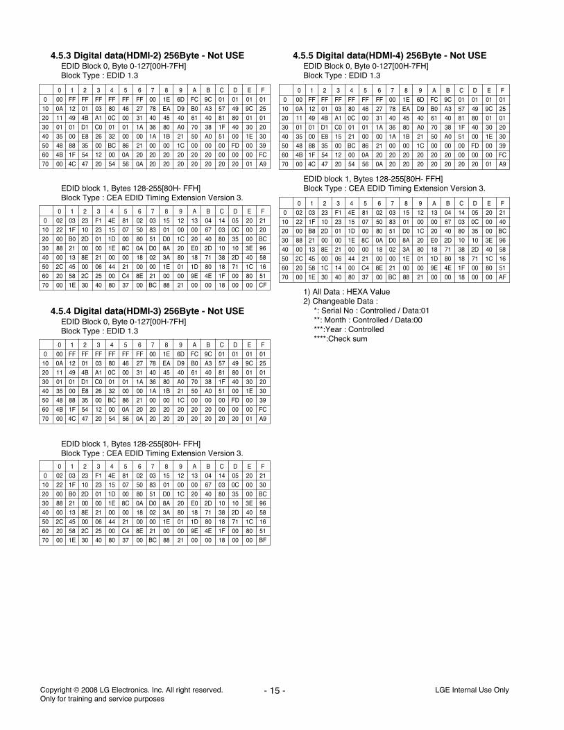
4.5.3 Digital data(HDMI-2) 256Byte - Not USEEDID Block 0, Byte 0-127[00H-7FH]Block Type : EDID 1.3
EDID block 1, Bytes 128-255[80H- FFH]Block Type : CEA EDID Timing Extension Version 3.
4.5.4 Digital data(HDMI-3) 256Byte - Not USEEDID Block 0, Byte 0-127[00H-7FH]Block Type : EDID 1.3
EDID block 1, Bytes 128-255[80H- FFH]Block Type : CEA EDID Timing Extension Version 3.
4.5.5 Digital data(HDMI-4) 256Byte - Not USEEDID Block 0, Byte 0-127[00H-7FH]Block Type : EDID 1.3
EDID block 1, Bytes 128-255[80H- FFH]Block Type : CEA EDID Timing Extension Version 3.
1) All Data : HEXA Value2) Changeable Data :
*: Serial No : Controlled / Data:01**: Month : Controlled / Data:00***:Year : Controlled****:Check sum
- 15 - LGE Internal Use OnlyCopyright © 2008 LG Electronics. Inc. All right reserved. Only for training and service purposes
0 1 2 3 4 5 6 7 8 9 A B C D E F0 00 FF FF FF FF FF FF 00 1E 6D FC 9C 01 01 01 01
10 0A 12 01 03 80 46 27 78 EA D9 B0 A3 57 49 9C 2520 11 49 4B A1 0C 00 31 40 45 40 61 40 81 80 01 0130 01 01 D1 C0 01 01 1A 36 80 A0 70 38 1F 40 30 2040 35 00 E8 26 32 00 00 1A 1B 21 50 A0 51 00 1E 3050 48 88 35 00 BC 86 21 00 00 1C 00 00 00 FD 00 3960 4B 1F 54 12 00 0A 20 20 20 20 20 20 00 00 00 FC70 00 4C 47 20 54 56 0A 20 20 20 20 20 20 20 01 A9
0 1 2 3 4 5 6 7 8 9 A B C D E F0 02 03 23 F1 4E 81 02 03 15 12 13 04 14 05 20 21
10 22 1F 10 23 15 07 50 83 01 00 00 67 03 0C 00 2020 00 B0 2D 01 1D 00 80 51 D0 1C 20 40 80 35 00 BC30 88 21 00 00 1E 8C 0A D0 8A 20 E0 2D 10 10 3E 9640 00 13 8E 21 00 00 18 02 3A 80 18 71 38 2D 40 5850 2C 45 00 06 44 21 00 00 1E 01 1D 80 18 71 1C 1660 20 58 2C 25 00 C4 8E 21 00 00 9E 4E 1F 00 80 5170 00 1E 30 40 80 37 00 BC 88 21 00 00 18 00 00 CF
0 1 2 3 4 5 6 7 8 9 A B C D E F0 00 FF FF FF FF FF FF 00 1E 6D FC 9C 01 01 01 01
10 0A 12 01 03 80 46 27 78 EA D9 B0 A3 57 49 9C 2520 11 49 4B A1 0C 00 31 40 45 40 61 40 81 80 01 0130 01 01 D1 C0 01 01 1A 36 80 A0 70 38 1F 40 30 2040 35 00 E8 26 32 00 00 1A 1B 21 50 A0 51 00 1E 3050 48 88 35 00 BC 86 21 00 00 1C 00 00 00 FD 00 3960 4B 1F 54 12 00 0A 20 20 20 20 20 20 00 00 00 FC70 00 4C 47 20 54 56 0A 20 20 20 20 20 20 20 01 A9
0 1 2 3 4 5 6 7 8 9 A B C D E F0 02 03 23 F1 4E 81 02 03 15 12 13 04 14 05 20 21
10 22 1F 10 23 15 07 50 83 01 00 00 67 03 0C 00 3020 00 B0 2D 01 1D 00 80 51 D0 1C 20 40 80 35 00 BC30 88 21 00 00 1E 8C 0A D0 8A 20 E0 2D 10 10 3E 9640 00 13 8E 21 00 00 18 02 3A 80 18 71 38 2D 40 5850 2C 45 00 06 44 21 00 00 1E 01 1D 80 18 71 1C 1660 20 58 2C 25 00 C4 8E 21 00 00 9E 4E 1F 00 80 5170 00 1E 30 40 80 37 00 BC 88 21 00 00 18 00 00 BF
0 1 2 3 4 5 6 7 8 9 A B C D E F0 00 FF FF FF FF FF FF 00 1E 6D FC 9C 01 01 01 0110 0A 12 01 03 80 46 27 78 EA D9 B0 A3 57 49 9C 2520 11 49 4B A1 0C 00 31 40 45 40 61 40 81 80 01 0130 01 01 D1 C0 01 01 1A 36 80 A0 70 38 1F 40 30 2040 35 00 E8 15 21 00 00 1A 1B 21 50 A0 51 00 1E 3050 48 88 35 00 BC 86 21 00 00 1C 00 00 00 FD 00 3960 4B 1F 54 12 00 0A 20 20 20 20 20 20 00 00 00 FC70 00 4C 47 20 54 56 0A 20 20 20 20 20 20 20 01 A9
0 1 2 3 4 5 6 7 8 9 A B C D E F0 02 03 23 F1 4E 81 02 03 15 12 13 04 14 05 20 2110 22 1F 10 23 15 07 50 83 01 00 00 67 03 0C 00 4020 00 B8 2D 01 1D 00 80 51 D0 1C 20 40 80 35 00 BC30 88 21 00 00 1E 8C 0A D0 8A 20 E0 2D 10 10 3E 9640 00 13 8E 21 00 00 18 02 3A 80 18 71 38 2D 40 5850 2C 45 00 06 44 21 00 00 1E 01 1D 80 18 71 1C 1660 20 58 1C 14 00 C4 8E 21 00 00 9E 4E 1F 00 80 5170 00 1E 30 40 80 37 00 BC 88 21 00 00 18 00 00 AF

4.6. HDCP (High-Bandwidth Digital Contents Protection)
SETTING (Scaler : Mstar)Because HDCP keyis built in HDCP exclusive EEPROM,Download progress is not needed.
HDCP-KEY0:0x8089 38 AE 0D ED 40 E6 BB FA 4E DE 51 FB 8E D9 AA34 A8 C4 EA D8 6C DC 5C 91 5C B1 A6 13 2B 8B 8BF7 46 CC 1C 88 20 A3 27 0E E1 28 84 89 39 A3 E236 86 CE 67 EB A0 F2 35 6B 86 F5 21 71 95 8A 77A1 28 77 97 D3 7B EF 5C 15 48 AA 9E 97 39 CD 9840 5E 68 56 66 EF C1 3C E1 8F 2A 82 DE 8F 52 CCA8 1F 37 D9 D4 C6 24 16 7E 42 FF 57 CD 6B E0 8600 1A F1 19 5A AF 37 97 86 BA 83 29 FE 41 A8 D5
A1:0x00F4 73 43 03 23 22 C5 28 96 9E 35 0D 67 A8 8B DD7A 89 38 E0 94 F0 FF F5 8F F3 4E 5C 82 09 F3 97EB 01 52 EC D8 98 5C 4F 43 2E E7 9F F5 85 6D 15B1 83 20 F8 5E D0 33 4F F0 C1 8F 65 77 3D 31 B2FB A1 6E CA A6 D3 A2 35 1D 16 41 C3 89 86 98 788E 3E C1 64 01 79 05 21 47 AF 6A 6F 5B E1 4D 2B2F CC 18 8E 42 DC 9A F8 3C D0 D0 57 04 FB 14 428C 54 9D A9 06 EB E7 48 E2 29 EF 7E FD F6 45 12AC E4 BC 45 67 A3 9B 65 A1 0E ED 1A 84 AD 49 87A2 77 3F 11 A7 1B D1 7F 25 36 6C 6F D3 DF 25 D0FB
4.7 Outgoing condition Configuration- fffff and make ship condition- When pressing IN-STOP key by Service remocontrol, Red
LED are blinked alternatively. And then Automatically turnoff. (Must not AC power OFF during blinking)
4.8 Internal pressureConfirm whether is normal or not when between powerboard's ac block and GND is impacked on 1.5kV(dc) or2.2kV(dc) for one second
5. Adjustment Command
5.1. I2C(100K BPS)5.2. COMMUNICATION START
# Until ACK BIT goes LOW, Repeat it.
5.3. Command formCommand form use DDC2AB standard communicationprotocol.
a. LEN : DATA BYTE number to sendb. CMD : Command language theat monitor executes.c. VAL : FOS DATAd. CS : Dada’s CHECKSUM that transmite. DELAY : 50Msf. A : Acknowledge
- 16 - LGE Internal Use OnlyCopyright © 2008 LG Electronics. Inc. All right reserved. Only for training and service purposes
START 6E A STOP 50Ms
START 6E A 50 A A A A A A A30 00 CS STOPLEN CMD VAL

5.4. Adjustment Commands(LENGTH=84) 5.5. EEPROM DATA READ(1) Signal TABLE
(2) Command Set
* Purpose : To read(84h) the appointment Address ofE2PROM by 128(80h)-byte
5.6. E2PROM Data Write(1) Signal TABLE
LEN : 84h+BytesCMD : 8EhADH : E2PROM Slave Address(A0,A2,A4,A6,A8), Not 00h
(Reserved by Buffer To EEPROM)ADL : E2PROM Sub Address(00~FF)Data : Write data
(2) Command Set
* Purpose1) EDID write : 16-byte by 16-byte, 8 order (128-byte)
write(TO “00 – 7F” of “EEPROM Page A4”).2) FOS Default write : 16-mode data (HFh, HFl, VF, STD,
HP, VP, Clk, ClkPh, PhFine) write3) Random Data write : write the appointment Address of
E2PROM.
5.7. VRAM Read- Send CMD(70h) to read Video RAM value from MICOM And
save its value to 128-Bytes Buffer(Common Buffer for theuse of EDID)
- Delay 500ms (Time to Wait and Read Video RAM from
MICOM)- Be transmitted the contents of MICOM’s 128-bytes Buffer to
PC. (128th Data is the CheckSum of 127-bytes data : That’s OK if the value of adding 128-bytes Data is Zero)
- 17 - LGE Internal Use OnlyCopyright © 2008 LG Electronics. Inc. All right reserved. Only for training and service purposes
Adjustment Contents CMD(hex) ADR VAL[HEX] Description
FACTORY ON E0 00 00 Factory mode on
FACTORY OFF E2 00 00 Factory mode off
EEPROM ALL INIT. E4 00 00 EEPROM All clear
EEPROM Read E7 00 00 EEPROM Read
EEPROM Write E8 00 data EEPROM Write by
some values
COLOR SAVE EB 00 00 Color Save
(R/G/B cutoff, Drive,
Contrast, Bright)
H POSITION 20 00 00 – 64 They have different
V POSITION 30 00 00 – 64 range each mode,
CLOCK 90 00 00 – 64 FOS Adjustment
PHASE 92 00 00 – 64
R DRIVE 16 00:cool 00 – 80 Drive adjustment
01:medium
02:warm
G DRIVE 18 00 :cool 00 – 80
01:medium
02:warm
B DRIVE 1A 00:cool 00 – 80
01:medium
02:warm
R CUTOFF 80 00 00 – 7F Offset adjustment
G CUTOFF 82 00 00 – 7F
B CUTOFF 84 00 00 – 7F
BRIGHT 10 00 00 – 3F Bright adjustment
CONTRAST 12 00 00 - 64 Luminance adjustment
AUTO_COLOR_ F1 00 02 Auto COLOR
ADJUST Adjustment
CHANGE_COLOR_ F2 00 0,1,2,3 0: Cool
TEMP 1: Medium
2: Warm
3: User
White Pattern F3 00 00,FF 00: White pattern off
FF: White pattern on
AUTO_ F4 00 0,10,20,30, 0 : TV
INPUTCHANGE 40,60,90 10 : DTV
20 : SCART1
30 : SCART2
40 : Component
60 : RGB
90 : HDMI
128 Bytes
Delay 100ms
EEPROM READ E7 A0 0 0-Page 0~7F Read
80 0-Page 80~FF Read
A2 0 1-Page 0~7F Read
80 1-Page 80~FF Read
A4 0 2-Page 0~7F Read
80 2-Page 80~FF Read
A6 0 3-Page 0~7F Read
80 3-Page 80~FF Read
Adjustment item CMD(hex) ADH(hex) ADL(hex) Details
EEPROM WRITE E8 94 16-Byte Write
84+n n-byte Write
Adjustment item CMD(hex) LEN Remark
70 00 00
6F A AData 1START Data 128 STOPNACS...

LGE Internal Use OnlyCopyright © 2008 LG Electronics. Inc. All right reserved. Only for training and service purposes
- 18 -
1. TV/CATV doesn’t display
2. DTV doesn’t display
TROUBLESHOOTING
Check TU401 Pin15(Video output), Pin16(Sound output)
Can you see the normal sign al?
Check th e output of TR(Q503).Can you see the normal waveform?
Check th e output of Main IC(IC100).Especially you should check
The H,V sync and c lock.Can you see the normal waveform?
YES
YES
NO Could you measu re voltag e of TU800 & IIC lines?
Are they all normal?
YES
NO You should ch eck p ower lin e & IIC li nes.
YES
You should rep lace TUNER.
NOYou should decid e to rep lace TR(Q503) or not.
NOAfter ch eckin g the Power of Main IC(IC100) you
should decide to replace Main IC or not .
This bo ard has b ig problem because Main IC(IC100) have some troubles.
After checking thoro ugh ly all pa th onc e again, You should decid e to rep lace Main Board or not.
Check th e output data o f TU800 Pin 24~34Can you see the normal sign al?
NO Could you measu re voltag e of TU800 & IIC lines?
Are they all normal?
NO You should ch eck p ower lin e & IIC li nes.
YES
You should rep lace TUNER.YES
Check th e output of Main IC(IC100).Especially you should check
The H,V sync and c lock.Can you see the normal waveform?
YES
NO After ch eckin g the Power of Main IC(IC100) you should decide to replace Main IC or not .
This bo ard has b ig problem because Main IC(IC100) have some troubles.
After checking thoro ugh ly all pa th onc e again, You should decid e to rep lace Main Board or not.

LGE Internal Use OnlyCopyright © 2008 LG Electronics. Inc. All right reserved. Only for training and service purposes
- 19 -
3. AV 1/2/3 doesn’t display
Check J6 00,J600,JK607,JK618Can you see the normal waveform?
Check th e input o f Video switch (IC700).Can you see the normal waveform?
YES
NOJ600,J601 or SIDE AV may have problem.
Replace th is Jack o r SIDE AV.
NOAfter ch eckin g the Power of AV switch you should decide to replace AV switch or not.
Check th e output of Main IC(IC100).Especially you should check
The H,V sync and c lock.Can you see the normal waveform?
YES
NO After ch eckin g the Power of Main IC(IC100) you should decide to replace Main IC or not .
This bo ard has b ig problem because Main IC(IC100) have some troubles.
After checking thoro ugh ly all pa th onc e again, You should decid e to rep lace Main Board or not.
YES
4. Component doesn’t display
Check J7 01.Can you see the normal waveform?
Check th e input o f Compo nent Audio switch (IC1001) ,
Can you see the normal waveform?
Check th e output of Component Audio switch (IC1001) ,
Can you see the normal waveform?
YES
YES
YES
NOJ701
may have problem. Rep lace th is Jack.
NO After checking the Power of compone nt Audio switch, y ou should decide to replace component
Audio s witch or not.
NO After checking the Power of compone nt Audio switch y ou should decide to replace component
Audio s witch or not.
Check th e output of Main IC(IC100).Especially you should check
The H,V sync and c lock.Can you see the normal waveform?
YES
NO After ch eckin g the Power of Main IC(IC100) you should decide to replace Main IC or not .
This bo ard has b ig problem because Main IC(IC100) have some troubles.
After checking thoro ugh ly all pa th onc e again, You should decid e to rep lace Main Board or not.
LGE Internal Use OnlyCopyright © 2008 LG Electronics. Inc. All right reserved. Only for training and service purposes
- 20 -
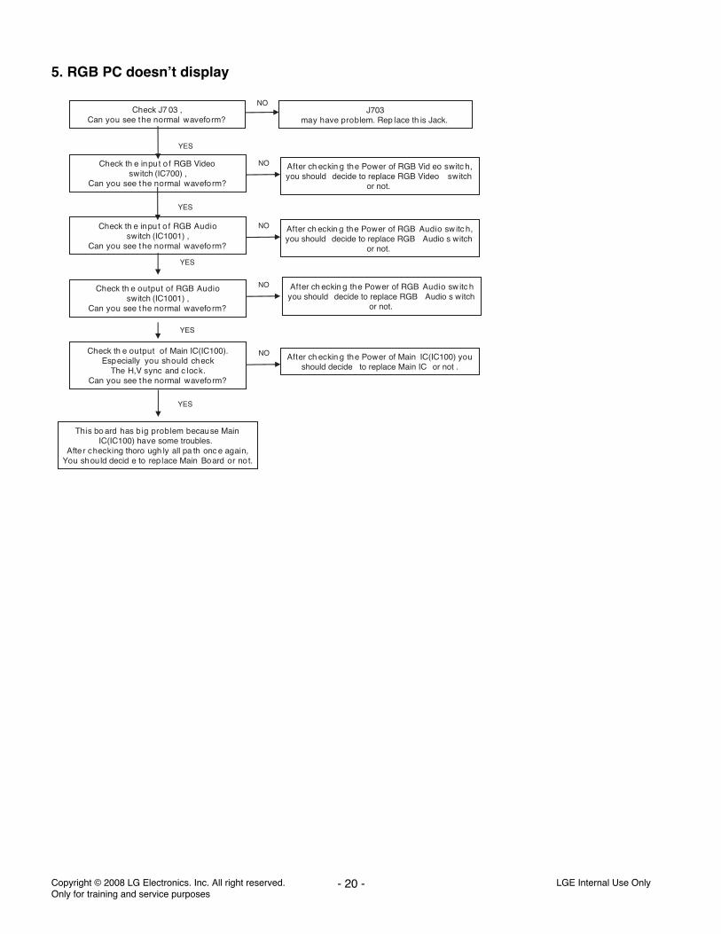
5. RGB PC doesn’t display
Check J7 03 ,Can you see the normal waveform?
Check th e input o f RGB Audio switch (IC1001) ,
Can you see the normal waveform?
Check th e output of RGB Audio switch (IC1001) ,
Can you see the normal waveform?
YES
YES
YES
NOJ703
may have problem. Rep lace th is Jack.
NO After ch eckin g the Power of RGB Audio sw itc h, you should decide to replace RGB Audio s witch
or not.
NO After ch eckin g the Power of RGB Audio sw itc h you should decide to replace RGB Audio s witch
or not.
Check th e output of Main IC(IC100).Especially you should check
The H,V sync and c lock.Can you see the normal waveform?
YES
NO After ch eckin g the Power of Main IC(IC100) you should decide to replace Main IC or not .
This bo ard has b ig problem because Main IC(IC100) have some troubles.
After checking thoro ugh ly all pa th onc e again, You should decid e to rep lace Main Board or not.
Check th e input o f RGB Video switch (IC700) ,
Can you see the normal waveform?
NO After ch eckin g the Power of RGB Vid eo switc h, you should decide to replace RGB Video switch
or not.
YES

- 21 - LGE Internal Use OnlyCopyright © 2008 LG Electronics. Inc. All right reserved. Only for training and service purposes
6. HDMI doesn’t display
Check input c onnect J900 , J901, J902Can you see the normal waveform?
Check DDC commu nication lin es(IC900, IC901, IC903 Pin5,6)
Check th e input o f HDMI Seitch (IC902)This sign al is TMDS.
Can you see the normal waveform?
YES
YES
NOJ900 , J901, J902
may have problem. Rep lace th is Jack.
Check th e output of HDMI Switc h(IC902).Can you see the normal waveform?
YES
YES
NO
After ch eckin g the trace o f TMDS lin es and power of HDMI Switch, you should decide to replace HDMI
Switch or not .
NO
NO
After ch eckin g the Power of th is ch ip , you should decide to replace this or not.
After ch eckin g the Power of HDMI Switch y ou should decide to replace MST3361 or not.
YES
Check HDCP commu nicatio n lin es(IC902)
NOAfter ch eckin g the Power of th is ch ip , you
should decide to replace this or not.
Check th e output of Main IC(IC100).Especially you should check
The H,V sync and c lock.Can you see the normal waveform?
YES
NO After ch eckin g the Power of Main IC(IC100) you should decide to replace Main IC or not .
This bo ard has b ig problem because Main IC(IC100) have some troubles.
After checking thoro ugh ly all pa th onc e again, You should decid e to rep lace Main Board or not.

LGE Internal Use OnlyCopyright © 2008 LG Electronics. Inc. All right reserved. Only for training and service purposes
- 22 -
BLOCK DIAGRAM
Sid
e Y
/C
Rea
r C
VB
S
CV
BS
_Out
IN1
IN3
IN1
IN3
OU
T1
Sid
e C
VB
S
AN
T
DV
B/P
AL
Tun
er
(TD
VS
-H70
2P)
LG In
note
k
M-S
TA
R(M
ST
2379
A/L
GE
7363
C)
D-A
MP
(YD
A13
8)0I
PR
PT
I030
B
Hea
dPho
ne
LVD
S(8
Bit)
X-T
AL
12M
hz62
12A
A20
04F
TV
_CV
BS
+(1
.8V
p-p)
$0.8
6
Aud
io_L
Aud
io_R
SIF
+(9
6dB
uV)
IN2
Air
: DV
B/P
AL
ïRG
B/Y
PbY
r*2
ïCV
BS
*2ïY
C*1
ïL/R
-IN
*3ïS
IFïC
VB
S O
UT
*1
R O
UT
L O
UT
0IM
MR
0014
1A
Hea
dP
hone
PC
(VG
A)
RS
232C
(Deb
ug)
L C D
US
B(S
W U
pgra
de)
CV
BS
0P
SIF
_IN
1P
SC
L_D
_TU
SD
A_D
_TU
TU
_TS
_CLK
TU
_TS
_SY
NC
TU
_TS
_VA
L
TS
1_C
LKT
S1_
SY
NC
TS
1_V
LD
IN[A
2]O
UT
[A1]
2
3.3V
1.8V
HP
_OU
T_L
[42]
HP
_OU
T_R
[1]
OU
T_P
_R[8
]O
UT
_N_R
[14]
OU
T_P
_L[3
5]O
UT
_N_L
[29]
IN_L
[38]
IN_R
[5]
HP
_DE
T[3
7]
MU
TE
[6]
AU
OU
TR
0[80
]A
UO
UT
L0[7
9]G
PIO
12[4
5]
LVD
S[1
77-1
90,
194-
199]
RX
E/R
XO
BIN
[1]S
OG
IN[2
]GIN
[3]R
IN[4
]V
S_R
GB
[7]
HS
_RG
B[8
]S
CL/
RX
[33]
SD
A/T
X[3
4]D
M_D
ET
[
PB
_IN
[11]
SO
Y[1
3]Y
_IN
[14]
PR
_IN
[16]
AU
L_IN
1[70
]A
UR
_IN
1[71
]
CV
BS
1[30
]A
UL_
IN0[
68]
AU
R_I
N[6
9]
SV
_C0[
25]
SV
_Y0[
26]
GP
IO15
[48]
6612
F00
099A
$0.2
7617
EA
G31
0220
01$0
.185
Tx/
Rx
(IC
603)
MA
X32
32C
DR
Tx_
Out
Rx_
InR
232C
_TX
D
R23
2C_R
XD
EE
PR
OM
AT
24C
028N
DD
C_S
DA
/UA
RT
_Tx
DD
C_S
CL/
UA
RT
_Rx
IR_R
X[5
7]S
AR
0[20
1]S
AR
1[20
2]S
AR
2[20
3]S
AR
3[20
4]
EE
PR
OM
(32K
)24
C32
EE
PR
OM
(32K
)24
C32
0IM
MR
AL
025A
RO
MS
CK
[35]
RO
MS
D[3
6]5V
Fla
sh(8
M*2
)F
lash
(8M
*2)
SP
I_C
K[1
71]
SP
I_D
I[172
]S
PI_
DO
[173
]S
PI_
CZ
[174
]
EA
N32
2134
01
3.3V
KE
Y_C
TL[
1,2,
3]
MP
1593
DN
-LF
0IP
MG
0006
3A
$0.4
6
12V
5V
Po
wer
/LIP
SP
ow
er/L
IPS
20îB
CM
: $2
023
îBC
M :
$18
20îB
B3
: $1
223
îBB
3 :
$18
Pow
er
Cha
nged
32K
512K
TU
_TS
_DA
TA
[0]
2.5V
TS
1_D
0
SC
L_A
_TU
SD
A_A
_TU V
ideo
SW
(IC
500,
S
TM
AV
340)
Com
p_1
YP
bPr
Com
p_2
YP
bPr
Com
p_Y
Com
p_P
b
Com
p_P
r
3 3
HY
5DU
5616
22(D
DR
)
HY
5DU
5616
22(D
DR
)
2.5_
DD
R
HY
5DU
5616
22(D
DR
)
HY
5DU
5616
22(D
DR
)

- 23 - LGE Internal Use OnlyCopyright © 2008 LG Electronics. Inc. All right reserved. Only for training and service purposes
Sid
e A
V_3
V,L
R
Rea
r C
VB
S_1
V, L
R
Sid
e S
_3Y
C
MN
T_V
,LR
_O
ut
IN1
IN3
IN1
IN3
OU
T1
Com
p_1
YP
bPr/
LR
Com
p_2
YP
bPr/
LR
Rea
r A
V_2
V, L
R
AN
T
DV
B/P
AL
Tun
er
(TD
VS
-H70
2P)
LG In
note
k
M-S
TA
R(M
ST
2379
A/L
GE
7363
C)
$4.6
6
D-A
MP
(NT
P30
00)
0IP
RP
TI0
30B
LVD
S(8
Bit)
CLK
_14.
3L6A
F62
12A
A20
04F
CV
BS
(AT
V)
$0.8
6
$0.0
623
Aud
io_L
Aud
io_R
SIF
IN2
Com
p1
Com
p2
Air
: 8V
SB
Cab
le :
256/
64Q
AM
ïRG
B/Y
PbY
r*2
ïCV
BS
*3ïY
C*2
ïL/R
-IN
*3ïS
IFïC
VB
S O
UT
*1
R O
UT
L O
UT
Hea
dP
hone
PC
Ear
Pho
ne
PC
(VG
A)
RS
232C
(Deb
ug)
PC
IN
L C D
US
B(S
W U
pgra
de)
1.8V
p-p
1.0V
p-p
96dB
uV
CV
BS
0[31
]B
uffe
r
SIF
_IN
1P
SIF
_IN
1M
SIF
_IN
1P
SIF
P0[
51]
Buf
fer
[11]
TS
0-7[
96,9
7,98
,99,
100,
101,
102,
103]
SC
L[48
]S
CL[
49]
MS
CL
MS
DA
SC
LM1[
59]
SD
AM
1[60
]
TP
CLK
[46]
TP
SO
P[4
4]T
PV
ALI
D[4
3]nT
PE
RR
[41]
TS
CLK
[95]
TS
SY
NC
[105
]T
SV
ALI
D[1
04]
IN[2
56] O
UT
[255
]
2
3.3V
1.8V
HP
_OU
T_L
[42]
HP
_OU
T_R
[1]
OU
T_P
_R[8
]O
UT
_N_R
[14]
OU
T_P
_L[3
5]O
UT
_N_L
[29]
IN_L
[38]
IN_R
[5]
HP
_DE
T[3
7]
MU
TE
[6]
12V
AU
OU
TR
0[80
]A
UO
UT
L0[7
9]G
PIO
12[4
5]
LVD
S[1
77-1
90,
194-
199]
RX
E/R
XO
BIN
[1]S
OG
IN[2
]GIN
[3]R
IN[4
]V
S_R
GB
[7]
HS
_RG
B[8
]S
CL/
RX
[33]
SD
A/T
X[3
4]D
M_D
ET
[A
UR
_IN
3[76
]A
UL_
IN3[
75]
PB
_IN
[11]
SO
Y[1
3]Y
_IN
[14]
PR
_IN
[16]
AU
L_IN
1[70
]A
UR
_IN
1[71
]
CV
BS
1[30
]A
UL_
IN0[
68]
AU
R_I
N[6
9]
SV
_C0[
25]
SV
_Y0[
26]
GP
IO15
[48]
6630
G70
016A
$0.2
3975
6630
G70
017A
$0.2
1984
6612
F00
099A
$0.2
7617
6612
F00
099A
$0.2
7617
EA
G31
0220
01$0
.185
6612
J100
31A
$0.2
5744
Tx/
Rx
(IC
L32
32)
0IP
RP
0000
9A0I
MX
2321
62A
$0.3
2$0
.4
ST
-5V
Tx_
Out
Rx_
In
R23
2C_T
x
R23
2C
_Rx
EE
PR
OM
0IM
MR
0001
4A$0
.076
DD
C_S
DA
DD
C_S
CL
IR_R
X[5
7]S
AR
0[20
1]S
AR
1[20
2]S
AR
2[20
3]S
AR
3[20
4]
EE
PR
OM
(32K
)24
C32
EE
PR
OM
(32K
)24
C32
0IM
MR
AL
025A
RO
MS
CK
[35]
RO
MS
D[3
6]5V
$0.1
45-
$0.7
6
Fla
sh(1
6M
)S
ST
25V
F01
6B
Fla
sh(1
6M
)S
ST
25V
F01
6B
SP
I_C
K[1
71]
SP
I_D
I[172
]S
PI_
DO
[173
]S
PI_
CZ
[174
]
EA
N32
2134
01
$0.6
7
3.3V
KE
Y_C
TL[
1,2,
3]
MP
1593
DN
-LF
0IP
MG
0006
3A
$0.4
6
12V
5V
Po
wer
/LIP
SP
ow
er/L
IPS
Pow
er
Cha
nged
32K
512K
SIF
HY
5DU
5616
22(D
DR
)
HY
5DU
5616
22(D
DR
)
2.5_
DD
R
HY
5DU
5616
22(D
DR
)
HY
5DU
5616
22(D
DR
)

- 24 - LGE Internal Use OnlyCopyright © 2008 LG Electronics. Inc. All right reserved. Only for training and service purposes
MS
D23
79A
[MS
TA
R]
DD
C_I
2C
E2P
ROM
_I2C
E2P
ROM
ED
ID /
ISP
I2C
MSC
L / M
SDA
IF_P
IF_N
SIF
TU
NE
R_C
VBS
IF_A
GC
Buf
fer
Buf
fer
LPF
TS
[0-7
]
TS_
CLK
TS_
SY
NC
TS_
VA
LID
I2C
MSC
L /
MS
DA
MA
IN I2
C
CV
BS_
0
SIF
TS_
DA
TA
Add
sy
nc p
atte
rn o
f ea
ch in
put/o
utpu
t
Add
det
ail
bloc
k di
agra
m o
f VS
B
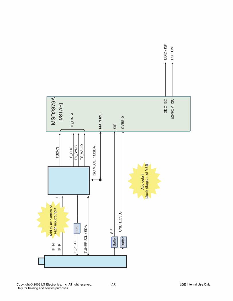
- 25 - LGE Internal Use OnlyCopyright © 2008 LG Electronics. Inc. All right reserved. Only for training and service purposes
MS
D23
79A
[MS
TA
R]
DD
C_I
2C
E2P
ROM
_I2C
E2P
ROM
ED
ID /
ISP
TU
NE
R S
CL
/ SD
A
IF_P
IF_N
SIF
TU
NE
R_C
VBS
IF_A
GC
Buf
fer
Buf
fer
LPF
TS
[0-7
]
TS_
CLK
TS_
SY
NC
TS_
VA
LID
I2C
MSC
L /
MS
DA
MA
IN I2
C
CV
BS_
0
SIF
TS_
DA
TA
Add
sy
nc p
atte
rn o
f ea
ch in
put/o
utpu
t
Add
det
ail
bloc
k di
agra
m o
f VS
B
- 26 - LGE Internal Use OnlyCopyright © 2008 LG Electronics. Inc. All right reserved. Only for training and service purposes
Sig
nal V
ideo A
V
S-V
ideo
AT
_TU
_V
Y/C
b/C
r_IN
Y/C
IN
CV
BS1
CV
BS0
CV
BS1
MS
tar
[MS
D23
79A
](F
rom
Tun
er)
SV
IDE
O (
Y/C
)
Com
pone
nt (
Y/C
b/C
r )
RG
BR
GB_
IN
Com
pone
nt
RG
B
LGDT
3303
LG
DT33
03
TS
Dat
aD
TV
_IN
Add
sy
nc p
atte
rn o
f ea
ch in
put/o
utpu
t
Add
det
ail
bloc
k di
agra
m o
f ea
ch V
ideo
inp
ut
- 27 - LGE Internal Use OnlyCopyright © 2008 LG Electronics. Inc. All right reserved. Only for training and service purposes
NTP
3000
MS
D23
79A
[MS
TA
R]
SPE
AK
ER
O
utpu
t
SIF
TS_
DA
TA
AU
_OU
T0_
L/R
AV
1_L
/R
CO
MPO
NEN
T_L
/R
DSU
B R
GB
_L/R
Add
sy
nc p
atte
rn o
f ea
ch in
put/o
utpu
t
Add
det
ail
bloc
k di
agra
m o
f ea
ch A
udio
inpu
t

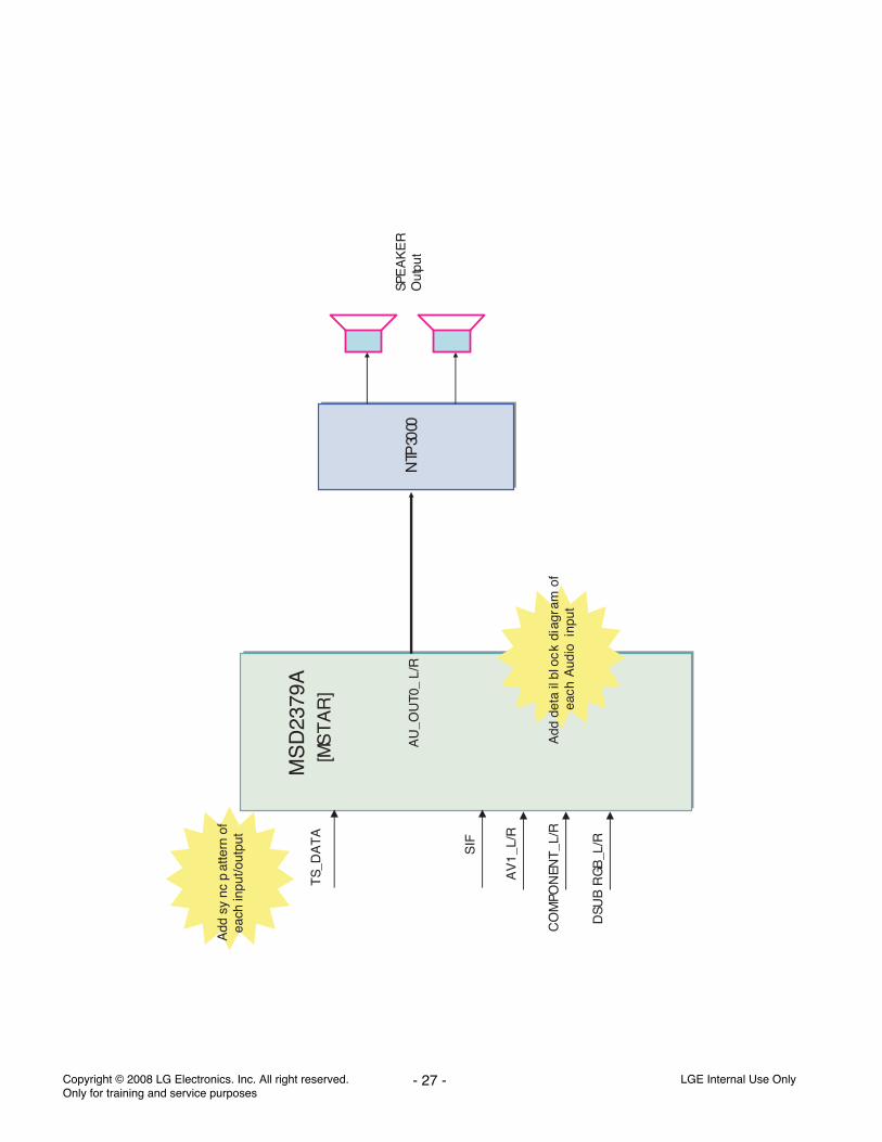
- 28 - LGE Internal Use OnlyCopyright © 2008 LG Electronics. Inc. All right reserved. Only for training and service purposes
M-S
TA
R[M
SD
2379
A]
IR Loca
lK
ey
57 IR IN
SA
R is
low
spe
ed 6
-Bits
AD
C in
pu
t an
d a
lso
for
GP
IO fu
nctio
n u
se.
Th
e I/O
tole
ranc
e is
3.3
V m
axim
um fo
r us
e.
Th
e ap
plic
atio
n of
A/
D k
ey, t
he
conv
ersi
on v
olta
ge fo
r fu
ll s
cale
of M
SD
1226
L is
1.8
V.
201
SA
R0
202
SA
R1
KE
Y_C
TL_
0
KE
Y_C
TL_
1

- 29 - LGE Internal Use OnlyCopyright © 2008 LG Electronics. Inc. All right reserved. Only for training and service purposes
Sou
nd A
mp
YD
A13
8
MS
D12
26L
VD
DC
AV
DD
_AD
CA
VD
D_S
IFA
VD
D_A
UA
VD
D_M
emP
LLA
VD
D_X
TA
LV
DD
_LP
LL
VD
DP
VD
DQ LG
DT
3303
VD
DA
VD
D
Vdd
33av
dd33
1 2 3 4 5 6 7 8 9 10 11 12
15V
15V
GN
D
5V AC
D
PW
R_O
N
INV
_CT
L
DIM
INV
_BR
6.3V
GN
D
5V
1 2 3 4 5 6 7 8 9 10 11
15V
15V
GN
D
5V NC
INV
_CT
L
DIM
INV
_BR
GN
D
5V GN
D
IC80
0M
P15
83D
N-Z
12V
Sou
nd M
ute
12V
Opt
ion
Pan
nel
23î
Out
put
Cur
ren
t : 3
AIn
put
: 4.
75V
to 2
3VO
utp
ut
: 1.
22V
to 2
1V
0.6A
0.4A
TU
NE
RIC
800
MP
1583
DN
-Z5V
12V
$0.4
6
265m
A
IC80
7K
IA78
R05
F
Out
put
Cur
ren
t : 1
AIn
put
: 7V
(Max
35V
)O
utp
ut :
5V$0.1
7
IC80
3A
Z11
17H
-3.3
V
IC80
4A
Z11
17H
-3.3
V
ST
_3.3
V
ST
_3.3
V
Fla
sh M
emor
yM
X25
L160
5AM
2C
SD
RA
MH
Y57
V64
1620
ET
P
IC80
2K
D10
84A
DT
-R
ST
_1.8
V
IR
IC80
6A
Z11
17H
-1.8
IC80
5A
Z11
17H
-3.3
1.8V
3.3V
Pan
nel
20î
FE
T52
03
0.4A
EE
PR
OM
AT
24C
32A
N
EE
PR
OM
AT
24C
02B
N
Out
put
Cur
ren
t : 1
A
Out
put
Cur
ren
t : 1
A
Out
put
Cur
ren
t : 5
A
Out
put
Cur
ren
t : 0
.6A
Out
put
Cur
ren
t : 0
.6A
274.
6mA
465m
A
72.4
mA
148.
8mA
570m
A
248m
A
800m
A

- 30 - LGE Internal Use OnlyCopyright © 2008 LG Electronics. Inc. All right reserved. Only for training and service purposes
Sou
nd A
mp
YD
A13
8
MS
D12
26L
VD
DC
AV
DD
_AD
CA
VD
D_S
IFA
VD
D_A
UA
VD
D_M
emP
LLA
VD
D_X
TA
LV
DD
_LP
LL
VD
DP
VD
DQ
MS
D80
9V
DD
VD
D
1 2 3 4 5 6 7 8 9 10 11 12
15V
15V
GN
D
5V AC
D
PW
R_O
N
INV
_CT
L
DIM
INV
_BR
6.3V
GN
D
5V
1 2 3 4 5 6 7 8 9 10 11
15V
15V
GN
D
5V NC
INV
_CT
L
DIM
INV
_BR
GN
D
5V GN
D
IC80
0M
P15
83D
N-Z
12V
Sou
nd M
ute
12V
Opt
ion
Pan
nel
23î
Out
put
Cur
ren
t : 3
AIn
put
: 4.
75V
to 2
3VO
utp
ut
: 1.
22V
to 2
1V
0.6A
0.4A
TU
NE
RIC
800
MP
1583
DN
-Z5V
12V
$0.4
6
265m
A
IC80
7K
IA78
R05
F
Out
put
Cur
ren
t : 1
AIn
put
: 7V
(Max
35V
)O
utp
ut :
5V$0.1
7
IC80
3A
Z11
17H
-3.3
V
IC80
4A
Z11
17H
-3.3
V
ST
_3.3
V
ST
_3.3
V
Fla
sh M
emor
yM
X25
L160
5AM
2C
SD
RA
MH
Y57
V64
1620
ET
P
IC80
2K
D10
84A
DT
-R
ST
_1.8
V
IR
IC80
7A
Z11
17H
-1.2
IC80
5A
Z11
17H
-3.3
1.2V
3.3V
Pan
nel
20î
FE
T52
03
0.4A
EE
PR
OM
AT
24C
32A
N
EE
PR
OM
AT
24C
02B
N
Out
put
Cur
ren
t : 1
A
Out
put
Cur
ren
t : 1
A
Out
put
Cur
ren
t : 5
A
Out
put
Cur
ren
t : 0
.6A
Out
put
Cur
ren
t : 0
.6A
274.
6mA
465m
A
72.4
mA
148.
8mA
570m
A
248m
A
800m
A

- 31 - LGE Internal Use OnlyCopyright © 2008 LG Electronics. Inc. All right reserved. Only for training and service purposes
AT
SC
/NT
SC
TU
NE
R
I2C
MS
D12
26L
SC
LM1[
59]
LGD
T33
03
3.3V
IIC
I2C
_SD
AI2
C_S
CL
SD
A[5
]
SC
L[6]
SD
AM
1[60
]M
SC
LM
SD
A
SC
L[48
]S
DA
[49]
5V II
C
DD
C_S
CK
[33]
DD
C_S
D[3
4]S
CL/
RX
SD
A/T
X
VG
A_R
XV
GA
_TX
EE
PR
OM
24C
32
DD
C_R
OM
SC
K[3
5]D
DC
_RO
MS
D[3
6]
RO
MS
CK
RO
MS
D
FLA
SH
S
ST
25V
F01
6B
SP
I_C
KS
PI_
DI
SP
I_D
OS
PI_
CZ
SP
I_C
K[1
71]
SP
I_D
I[172
]S
PI_
DO
[173
]S
PI_
CZ
[174
]
VG
AD
-SU
B
VG
AD
-SU
B
EE
PR
OM
24C
21A
DD
C_S
CL
DD
C_D
SA
UA
TX
1[55
]U
AR
X1[
56]
SD
RA
M4M
*16B
it
SD
RA
M4M
*16B
it
SD
RA
M4M
*16B
it
M2_
CK
EM
2_M
CLK
M2_
A[0
:11]
M2_
DQ
[0:1
5]M
2_D
QM
0M
2_D
QM
1C
KE
MC
LK
AR
[0:1
1]M
DA
TA
[0:1
5]D
QM
0D
QM
1C
KE
MC
LK
AR
[0:1
1]M
DA
TA
[16:
31]
DQ
M0
DQ
M1
Deb
ug
Por
t
RX
D
TX
D
GN
D
5V

- 32 - LGE Internal Use OnlyCopyright © 2008 LG Electronics. Inc. All right reserved. Only for training and service purposes
Mst
ar
[MS
D12
26L
]
AT
SC
/NT
SC
Tu
ner
LGD
T 3
303
MS
CL/
MS
DA
I2C
_5V
4.7K5V
ST
NV
RA
M
I2C
Add
ress
0xC
2
0x1C
Mst
ar
[MS
D12
26L
]M
X25
L160
5[S
eria
l Fla
sh]
SC
K
SD
I
SD
O
CS
Z
SP
I_C
K
SP
I_D
I
SP
I_D
O
SP
I_C
SZ
SC
LK
SI
SO
CS
#
4.7K+3.
3V
DD
C_R
OM
SC
L/S
DA
0xA
0

LGE Internal Use OnlyCopyright © 2008 LG Electronics. Inc. All right reserved. Only for training and service purposes
- 33 -
MEMO
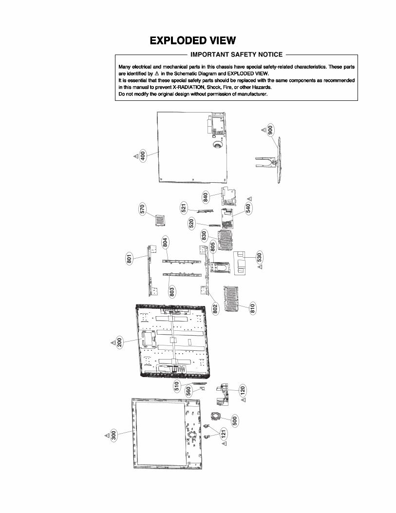
300
200
801
400
900
540
530
810
120
500
570
121
56051
080
380
4
840
520
521
830
805
802
EXPLODED VIEW
Many electrical and mechanical parts in this chassis have special safety-related characteristics. These partsare identified by in the Schematic Diagram and EXPLODED VIEW. It is essential that these special safety parts should be replaced with the same components as recommendedin this manual to prevent X-RADIATION, Shock, Fire, or other Hazards. Do not modify the original design without permission of manufacturer.
IMPORTANT SAFETY NOTICE

THE
S
YMBO
L MA
RK O
F TH
IS S
CHEM
ETIC
DIA
GRAM
INC
ORPO
RATE
SSP
ECIA
L FE
ATUR
ES I
MPOR
TANT
FOR
PRO
TECT
ION
FROM
X-R
ADIA
TION
.FI
LRE
AND
ELEC
TRIC
AL S
HOCK
HAZ
ARDS
, WH
EN S
ERVI
CING
IF
IS
ESSE
NTIA
L TH
AT O
NLY
MANU
FATU
RES
SPEC
FIED
PAR
TS B
E US
ED F
ORTH
E CR
ITIC
AL C
OMPO
NENT
S IN
THE
SYMB
OL M
ARK
OF T
HE S
CHEM
ETIC
.
MS_LRCK
008:H16
LED_G
010:E8
SDA_EYEQ/AMP
008:H16;007:AD7;010:O14
R1056
100
C139
0.047uF
C147
0.1uF
R1078
100
C146
0.1uF
C101
10uF
16V
3216
C117
0.047uF
R1051
47
RS232C_TXD
C145
0.1uF
C126
2.2uF
16V
R1005
1M
+3.3V_VDDP_ST
C116
0.047uF
SIDE_L_IN
R1045
100
C144
0.1uF
R1117
4.7K
SIDE_C_IN
R1062
47
HDMI_RX1-
R1107
22
C140
0.047uF
BOOSTER
R1057
3.3K
OPT
R1106
100
R1075
100
MUTE
008:S16
R1090
100
C131
2.2uF
16V
R1082
1K
OPT
HDMI_RX2-
R1093
100
C127
2.2uF
16V
PANEL_CTL
SPI_SCK
AC_DET
SCL_A_TU
KEY2
010:H13
HDMI_RX0+
A_DIM
001:B6;009:H14
C114
0.047uF
HDMI_RX0-
SYSTEM_SDA
001:S5;001:AB11
LED_R
010:E7
EYEQ_RESET
010:P9
R1097
100
HDMI_CLK+
TU_RESET_N
004:J11
R1003
22K
R1102
100
R1068
100
R1055
100
Flash_WP_1
001:AC18
5V_HDMI_2
R1027
47
C130
2.2uF
16V
R1037
47
R1047
100
DSUB_G
R1111 0
R1052
10K
OPT
R1086
100
C141
0.047uF
R1067
22
R1028
47
R1069
100
R1079
100
DSUB_B
X100
12MHz
USB_CTL
006:AE24
R1095
100
HDMI_SDA
007:AG24
R1063
47
R1073
100
C125
2.2uF
16V
PC_L_IN
C151
0.1uF
SCL_EYEQ/AMP
R1018
10K
R1101
100
+3.3V_AVDD_DVI
009:AB11
R1108
100OPT
R1074
100
MS_SCK
008:H16
R1016
1K
R1024
0
R1032
47
A_DIM
001:G12;009:H14
C120
0.047uF
C123
0.1uF
R1064
100
R1060
100
C106
4.7uF
16V
3216
C115
0.047uF
R1017
10K
OPT
+5V_ST
C124
2.2uF
16V
R1042
47
R1119
100
R1070
22
R1096
100
C135
0.047uF
R1015
1K
OPT
INV_CTL
009:H14;009:K17
R1058
100
R1066
100
C137
0.047uF
C121
0.047uF
C109
1uF
25V
R1080
22
R1116
4.7K
SPI_SDI
PWM_LED
001:G12;010:P10
SIF+
R1110
3.3K
OPT
COMP_Pr 005:M17
R1092
100
DDC_SDA/UART_TX
SPDIF_OUT
008:C27
R1030
47
C119
0.047uF
R1033
47
C129
2.2uF
16V
AUDIO_MASTER_CLK
008:H22
R1009
0
R1054
100
R1038
470
R1109
100
SPI_SDO
COMP_Y
R1072
100
+3.3V_VDDP_ST
EEPROM_WP
R1115
0
COMP_R
5V_HDMI_3
R1100
100
DSUB_VSYNC
HDMI_RX1+
007:AI23
C128
2.2uF
16V
R1022
100
SYSTEM_SCL
001:H28;001:AB11
PWM_DIM
009:D13
DSUB_HSYNC
005:R16
IR
010:H10
DDC_SCL/UART_RX
005:AB18
C138
1000pF
SDA_A_TU
004:K16;004:L3;004:R8
R1050
910
1%
R1046
100
RL_ON
009:B5;009:E16
R1004 0
2012
R1094
100
R1040
470
RS232C_RXD
006:M22
R1012
1K
OPT
HDMI_CLK-
007:AG23
HDMI_SCL
C148
0.047uF
R1059
100
R1114
0
OPT
R1104
100
C149
0.047uF
SYSTEM_SDA
001:H28;001:AB11
R1077
100
KEY1
010:H14
IC103
AT24C512W-10SI-2.7
3NC
2A1
4GND
1A0
5SDA
6SCL
7WP
8VCC
R1081
22
PWM_LED
001:B6;010:P10
R1088
100
SIDE_CVBS_IN
R1084
100
AMP_RST
008:H22
PC_R_IN
SPI_CSN_2
001:W15
DSUB_R
MODULE_SEL
001:J6
C118
0.047uF
+3.3V_VDDP_ST
MS_LRCH
008:H17
+3.3V_VDDP_ST
R1035
100
R1061
47
R1002
22K
R1083
100
Flash_WP_2
001:AD15
SDA_D_TU
SCL_D_TU
003:M14;004:H13;001:AB5;001:AM5
R1021
100
COMP_L
C104
0.01uF
R1039
47
C122
0.1uF
R1118
100
R1043
47
R1112
0
HDMI_CEC
COMP_SEL
005:L18;008:E6;008:O10
R1034
47
R1113
0
OPT
R1031
47
R1023
0
R1065
100
USB_DM
R1085
22
USB_DP
006:X25
SIDE_R_IN
R1041
47
C150
0.047uF
R1011
1K
HPD
007:AF24
R1048
100
R1071
100
R1029
475V_MNT
009:J15
R1044
47
SYSTEM_SCL
C142
0.047uF
SPI_CSN_1
001:X18
C102
0.1uF
50V
COMP_Pb
R1105
100
OPT
TV_CVBS+
HDMI_RX2+
5V_HDMI_1
SIDE_Y_IN
MODULE_SEL
001:J12
C136
1000pF
C105
0.01uF
Q100
2SC3052
E
B
C
+3.3V_VDDP_ST
C143
22pF
50V
OPT
C134
22pF
50V
OPT
C113
22pF
50V
OPT
C112
22pF
50V
OPT
R1076
390
R1087
0R1089
0
R1098
0R1099
0
MDATA[13]
LVA_1M
DQM2
LVB_0M
MDATA[22]
MADR[5]
LVB_4M
LVB_CKP
MADR[4]
MDATA[16]
CLKE
MDATA[1]
MDATA[23]
MDATA[7]
LVB_3P
LVB_2M
R1155
56
MDATA[0]
LVB_CKM
AR102
22
1/16W
R1153
56
MADR[8]
M_CAS
LVA_CKM
R1142
56
R1146
56
MDATA[5]
LVA_2M
AR101
22
1/16W
BA1
MDATA[19]
MCLK+
MDATA[21]
DQM3
DQM1
MDATA[28]
MADR[3]
MADR[10]
R1149
56
R1143
56
R1148
56
LVB_0P
M_RAS
LVA_4M
DQS1
MDATA[10]
MDATA[3]
MDATA[17]
MDATA[11]
LVA_1P
MDATA[30]
MDATA[8]
M_WE
AR104
22
1/16W
MDATA[31]
LVB_1M
LVA_0P
R1147
56
LVA_CKP
R1145
56
R1157
56
R1144
56
R1154
56
1
LVA_3P
MDATA[4]
R1152
56
MDATA[27]
AR106
22
1/16W
MDATA[26]
MADR[0]
R1156
56
MDATA[25]
LVB_2P
LVB_4PMADR[1]
MDATA[2]
DQS2
BA0
MCLK-
DQS0
MADR[9]
MDATA[14]
LVA_3M
LVB_1P
MDATA[29]
LVB_3M
MDATA[9]
LVA_0M
R1150
56
AR103
22
1/16W
MDATA[6] MDATA[12]
DQM0
MDATA[15]
MADR[6]
MADR[7]
MADR[2]
R1158
56
R1141
56
MADR[11]
MADR[12]
LVA_2P
MDATA[20] MDATA[24]
MDATA[18]
R1151
56
DQS3
LVA_4P
AR105
22
1/16W
R1121
1K
1%
+3.3V_AVDD_OTG
C160
0.1uF
50V
+3.3V_AVDD_LPLL
C163
1000pF
+3.3V_AVDD_SIF
+1.25V_VDDC
C168
0.1uF
50V
+3.3V_AVDD_ADC
+3.3V_AVDD_AU
C155
0.1uF
50V
+2.5V_VDD_DDR
C152
0.1uF
50V
+1.25V_AVDD_DVI
C157
0.1uF
50V
C164
0.1uF
+3.3V_AVDD_MPLL
C169
0.1uF
50V
C153
0.1uF
50V
C156
0.1uF
50V
C154
0.1uF
50V
C167
0.1uF
50V
R1120
1K
1%
C162
0.1uF
50V
+3.3V_VDDP
C158
0.1uF
50V
C159
0.1uF
50V
+3.3V_AVDD_MEMPLL
C161
0.1uF
50V
+2.5V_VDD_DDR
C165
0.1uF
50V
R1008
100
R1007
100
C132
0.047uF
C133
0.047uF
R1025
47
R1026
47
AV_L_OUT006:AN10
AV_R_OUT
006:AN5
AV_CVBS_OUT
C111
0.1uF
IC101
KIA7027AF
2
G
3O
1I
+3.3V_VDDP_ST
+3.3V_VDDP_ST
C103
1uF
10V
IC102
74LX1G14CTR
3GND
21A
41Y
1NC
5VCC
SW100
TMUE312GAB
OPT
12 4
3
5
R1001
1K
MUTE_AV_L/R
006:AM7
+3.3V_VDDP_ST
SPI_CSN_1
Flash_WP_2
R1122
100
SPI_SDI
C166
0.1uF
R1123
4.7K
Flash_WP_1
+3.3V_VDDP_ST
SPI_SCK
SPI_SDO
+3.3V_VDDP_ST
R1126
100
C170
0.1uF
R1125
100
SPI_CSN_2
R1133
100
R1132
100
FRC_RESET
C1002
47uF
16V
SDA_D_TU
003:M14;004:H13;001:H25;001:AB6
DSUB_DET
005:AB15
R1178
100
FRC
EN_3.3VF
SDA_D_TU
003:M14;004:H13;001:H25;001:AM6
R1134
100
R1173
100
FRC
R1172
100
FRC
R1180
100
OPT
R1174
0
OPT
SIDE_CVBS_DET
006:I21
R1175
0
OPT
R1135
100
R1167
100
R1183
22
FRC
SCL_D_TU
003:M14;004:H13;001:H25;001:AB5
EN_2.5VF
R1137
100
R1170
100
FRC
C1001
0.1uF
EN_1.8VF
USB_OCD
006:AK24
IC106
JLC1562BFEL
3A2
2A1
4D0
1A0
6D2
5D1
7D3
8Vss
9D4
10
D5
11
D6
12
D7
13
VDAC
14
SCL
15
SDA
16
VDD
SCL_D_TU
003:M14;004:H13;001:H25;001:AM5
R1171
100
FRC
R1179
100
OPT
LVDS_SEL
EN_1.3VF
R1136
100
FRC_RESET
R1168
22
R1176
0
FRC
R1166
100
EN_1.3PLL
R1169
22
R1164
100
COMP2_DET
005:G11
+5V_TU
COMP1_DET
005:R9
IC108
JLC1562BFEL
FRC
3A2
2A1
4D0
1A0
6D2
5D1
7D3
8Vss
9D4
10
D5
11
D6
12
D7
13
VDAC
14
SCL
15
SDA
16
VDD
R1182
22
FRC
R1163
100
R1181
100
FRC
BIT_SEL
R1165
100
OPT
SIDE_Y/C_DET
006:H13
R1177
100
FRC
R1019
2.7K
R1020
2.7K
R1103
22
R1091
22
R1014
4.7K
AUS_ONLY
R1013
10K
OPT
R1006
10K
OPT
R1131
4.7K
+3.3V_VDDP_ST
SPK_N
SPK_P
TU_TS_VAL
TU_TS_SYNC
TU_TS_DATA[0]
TU_TS_CLK
IC105
S25FL064A
Flash_Memory
EAN42961201
3NC_1
2VCC
4NC_2
1HOLD
6NC_4
5NC_3
7CS
8SO
9W
10
GND
11
NC_5
12
NC_6
13
NC_7
14
NC_8
15
SI
16
SCK
IC107
S25FL064A
Flash_Memory
EAN42961201
3NC_1
2VCC
4NC_2
1HOLD
6NC_4
5NC_3
7CS
8SO
9W
10
GND
11
NC_5
12
NC_6
13
NC_7
14
NC_8
15
SI
16
SCK
R1184
2.2KNON_YAMAHA
R1185
10K
NON_YAMAHA
C1003
0.01uFNON_YAMAHA
R1186
10K
OPT
R1187
22
R1188
22
+5V_ST
R11244.7KFRC
+3.3V_CI
R11274.7KFRC
R11284.7KFRC
R11294.7KFRC
R11404.7K FRC
+3.3V_CI
R11304.7K OPT
R11384.7K OPT
R11394.7K FRC
IC100
LGE7363C-LF
SDR_CKE
A14
SDR_CKL+
C15
SDR_CLK-
B15
SDR_DQS_0
B7
SDR_DQM_0
A7
SDR_DQ_0
B3
SDR_DQ_1
A3
SDR_DQ_2
B4
SDR_DQ_3
A4
SDR_DQ_4
B5
SDR_DQ_5
A5
SDR_DQ_6
B6
SDR_DQ_7
A6
SDR_DQS_1
B12
SDR_DQM_1
A12
SDR_DQ_8
B8
SDR_DQ_9
A8
SDR_DQ_10
B9
SDR_DQ_11
A9
SDR_DQ_12
B10
SDR_DQ_13
A10
SDR_DQ_14
B11
SDR_DQ_15
A11
SDR_DQS_2
A20
SDR_DQM_2
B20
SDR_DQ_16
B16
SDR_DQ_17
A16
SDR_DQ_18
B17
SDR_DQ_19
A17
SDR_DQ_20
B18
SDR_DQ_21
A18
SDR_DQ_22
B19
SDR_DQ_23
A19
SDR_DQS_3
G19
SDR_DQM_3
G20
SDR_DQ_24
C19
SDR_DQ_25
C20
SDR_DQ_26
D19
SDR_DQ_27
D20
SDR_DQ_28
E19
SDR_DQ_29
E20
SDR_DQ_30
F19
SDR_DQ_31
F20
SDR_CASZ
E10
SDR_RASZ
D10
SDR_WEZ
C10
SDR_BA0
E11
SDR_BA1
D11
SDR_AD12
E13
SDR_AD11
D13
SDR_AD10
E12
SDR_AD9
D12
SDR_AD8
C12
SDR_AD7
C11
SDR_AD6
C13
SDR_AD5
B13
SDR_AD4
A13
SDR_AD3
E14
SDR_AD2
D14
SDR_AD1
C14
SDR_AD0
D15
RXO0-
H19
RXO0+
H20
RXO1-
J19
RXO1+
J20
RXO2-
K19
RXO2+
K20
RXOC-
L19
RXOC+
L20
RXO3-
M19
RXO3+
M20
RXO4-
N19
RXO4+
N20
RXE0-
P19
RXE0+
P20
RXE1-
R19
RXE1+
R20
RXE2-
T19
RXE2+
T20
RXEC-
U19
RXEC+
U20
RXE3-
V19
RXE3+
V20
RXE4-
W19
RXE4+
W20
TS1_CLK
J16
TS1_SYNC
H16
TS1_VLD
H17
TS1_D0
K18
TS0_CLK
Y7
TS0_SYNC
W7
TS0_VLD
V7
TS0_D7
U7
TS0_D6
T7
TS0_D5
Y6
TS0_D4
W6
TS0_D3
V6
TS0_D2
U6
TS0_D1
T5
TS0_D0
T6
PCM_A0
Y12
PCM_A1
W12
PCM_A2
V12
PCM_A3
U12
PCM_A4
Y11
PCM_A5
W11
PCM_A6
V11
PCM_A7
U11
PCM_A8
T11
PCM_A9
Y10
PCM_A10
W10
PCM_A11
V10
PCM_A12
U10
PCM_A13
T10
PCM_A14
Y9
PCM_D0
V9
PCM_D1
U9
PCM_D2
T9
PCM_D3
Y8
PCM_D4
W8
PCM_D5
V8
PCM_D6
U8
PCM_D7
T8
PCM_IORD
P16
PCM_IOWR
R16
PCM_OE_N
M17
PCM_WE_N
N17
PCM_REG_N
T17
PCM_CE_N
V18
PCM_IRQA
P18
PCM_WAIT_N
T18
PCM_RESET
N16
PCM_CD_N
K16
IC100
LGE7363C-LF
GPIO0/UART_RX1/CEC
C4
GPIO1/UART_TX1
D4
DDCR_DAT
V15
DDCR_CLK
W15
DDC_SDA/UART-TX
T15
DDC_SCL/UART-RX
U15
GPIO3
E4
SD/MS_D0
U16
SD/MS_D1
R17
SD/MS_D2
U18
SD/MS_D3
N18
SD_SPDZ
R18
SD_CMD
T16
SD/MS_CLK
P17
SD_OCDT
U17
SD_PWRCTL
V17
SD_MS_INS
M16
SD_CDZ
L16
INT/GPIO4
T14
GPIO14/UART_TX1
E16
I2S_IN_BCK/GPIO24
G18
I2S_IN_WS/GPIO23
F18
LVSYNC/GPIO22
K17
LHSYNC/GPIO21
J17
LDE/GPIO20
M18
LCK/GPIO19
L18
DOUT_CLK/GPIO20
Y3
DIN_D3/GPIO28
V5
DIN_D2/GPIO27
U5
DIN_D1/GPIO26
Y4
DIN_D0/GPIO25
W4
DOUT_3/GPIO24
V4
DOUT_2/GPIO23
U4
DOUT_1/GPIO22
W3
DOUT_0/GPIO21
V3
TCON_EXT3/GPIO19
D6
TCON_EXT2/GPIO18
C6
TCON_EXT1/GPIO17
D5
TCON_EXT0/GPIO16
C5
INT2/GPIO26
H18
IRIN2/GPIO25
J18
TESTPIN
E6
XTALI
A2
XTALO
A1
USB_DP
P4
USB_DM
N4
USB_REXT
C7
RESET
Y15
XIN_RTC
W5
XOUT_RTC
Y5
IRIN/GPIO3
T13
RXCN
B2
RXCP
B1
RX0N
C2
RX0P
C1
RX1N
D2
RX1P
D1
RX2N
E2
RX2P
E1
HOTPLUGA
G5
REXT
E3
DDCDA_DA
E5
DDCDA_CK
F5
I2S_OUT_MUTE/CEC
E17
HSYNC1
G1
VSYNC1
G2
VCLP
F3
REFP
F2
REFM
F1
BIN1P_1
H1
SOGIN1
H2
GIN1P
H3
BIN1P_2
J1
BIN0M
J2
BIN0P
J3
GIN0M
K1
GIN0P
K2
SOGIN0M
F4
RIN0M
K3
RIN0P
L1
HSYNC0
J4
VSYNC0
K4
C1(CVBS7P)
L4
Y1(CVBS5P)
L2
C0(CVBS6P)
L3
Y0(CVBS4P)
M1
CVBS3P
G4
CVBS2P
N3
CVBS1P
M4
VCOM1
N2
CVBS0P
G3
VCOM0
M2
CVBS_OUT
N1
SIF_IN1P
P1
SIF_IN1M
P2
LINE_IN_0L
R1
LINE_IN_0R
R2
LINE_IN_1L
R3
LINE_IN_1R
R4
LINE_IN_2L
T1
LINE_IN_2R
T2
LINE_IN_3L
T3
LINE_IN_3R
T4
VIM0
R5
AUVRM
U3
AUVRP
U2
AUVAG
U1
LINE_OUT_2L
V1
LINE_OUT_2R
V2
LINE_OUT_1L
W1
LINE_OUT_1R(DACO_S)
W2
LINE_OUT_0L(DACO_L)
Y1
LINE_OUT_0R(DACO_R)
Y2
SAR0
W13
SAR1
Y13
SAR2
W14
SAR3
Y14
PWM0
U13
PWM1
V13
PWM2
U14
PWM3
V14
SPDIF_IN
G17
SPDIF_OUT
E15
I2S_OUT_SD
D17
I2S_OUT_BCK
C17
I2S_OUT_WS
G16
I2S_OUT_MCK
F16
I2S_IN_SD
F17
NC_1
M3
NC_2
W9
SPI_CK1
Y18
SPI_DI1
Y16
SPI_DO1
Y19
SPI_CZ1
Y17
IC100
LGE7363C-LF
VSS_1
M12
VSS_2
M11
VSS_3
M10
VSS_4
M9
VSS_5
M8
VSS_6
L12
VSS_7
L11
VSS_8
L10
VSS_9
L9
VSS_10
L8
VSS_11
K12
VSS_12
K11
VSS_13
K10
VSS_14
K9
VSS_15
K8
VSS_16
J12
VSS_17
J11
VSS_18
J10
VSS_19
J9
VSS_20
J8
VSS_21
C3
VSS_22
D3
VSS_23
H4
VSS_24
C8
VSS_25
C9
VSS_26
D8
VSS_27
D9
VSS_28
E8
VSS_29
E9
VSS_30
C16
VSS_31
D16
VSS_32
C18
VSS_33
D18
VSS_34
E18
VSS_35
T12
VSS_36
V16
VSS_37
W16
VSS_38
W17
VSS_39
W18
VSS_40
Y20
IC100
LGE7363C-LF
VD33_1
P11
VD33_2
P12
VD33_3
P13
VD33_4
P14
VD33_2_1
P9
VD33_2_2
P10
AVDD_33_1
G6
AVDD_33_2
H6
AVDD_33_3
J6
AVDD_33_4
K6
AVDD_33_5
L6
AVDD_33_6
G7
AVDD_MPLL
E7
AVDD_MEMPLL
B14
AVDD_USB
D7
AVDD_LPLL_1
G12
AVDD_LPLL_2
L17
AVDD_AU
P6
AVDD_SIF
P3
AVDD_DDR_1
G13
AVDD_DDR_2
G11
AVDD_DDR_3
G10
MVREF
A15
AVDD_DVI_1
G8
AVDD_DVI_2
G9
VDDC_1
M6
VDDC_2
N6
VDDC_3
G14
VDDC_4
H14
VDDC_5
J14
VDDC_6
K14
VDDC_7
L14
VDDC_8
M14
VDDC_9
N14
VDD_PWR
P7
AVDD_RTC
P8
R1036
0
MUTE_YAMAHA
008:AL9YAMAHA_GAIN0
008:AK10
R1010
10K
C110
4.7uF
6.3V
5V_HDMI_4
007:R11;007:W23;007:AD24
YAMAHA_GAIN1
008:AK11
R1049
0
C107
27pF
C108
27pF
PS421/NTP_SCL
PS421/NTP_SDA
FRAME_SEL
+3.3V_CI
R11594.7K
OPT
+3.3V_VDDP_ST
SYSTEM_SCL
001:H28;001:S5
SYSTEM_SDA
001:H28;001:S5
IC109
CAT24WC08W-T
3A2
2A1
4VSS
1A0
5SDA
6SCL
7WP
8VCC
R127
4.7K
C171
0.1uF
R126
22
R125
22
PS421_RST
008:AK10
X
//BOOTSTRAP PWM[1:0]=10
R1055
EEPROM
R1081
VIDEO IN
O
0V
AUDIO IN
O
O
42"/47" FHD
OX
R1110
26'HD
X
R1051
O
0.77
R1109
MODULE SELECT
X
I2S
52" Sharp
GPIO
AUDIO OUT
XO
1.65
XX
XX
XX
X2.48
X
O32/37/42/47HD
FLASH
HDMI
DDR MEMORY LVDS
TS SIGNAL
ST_BY 3.3V
VIDEO OUT
FLASH MEMORY
I/0 EXPANSION-2
I/0 EXPANSION-1
HDCP EEPROM
SCHEMATIC DIAGRAM
Copyright ©2008 LG Electronics. Inc. All right reserved. Only for training and service purposes
LGE Internal Use Only
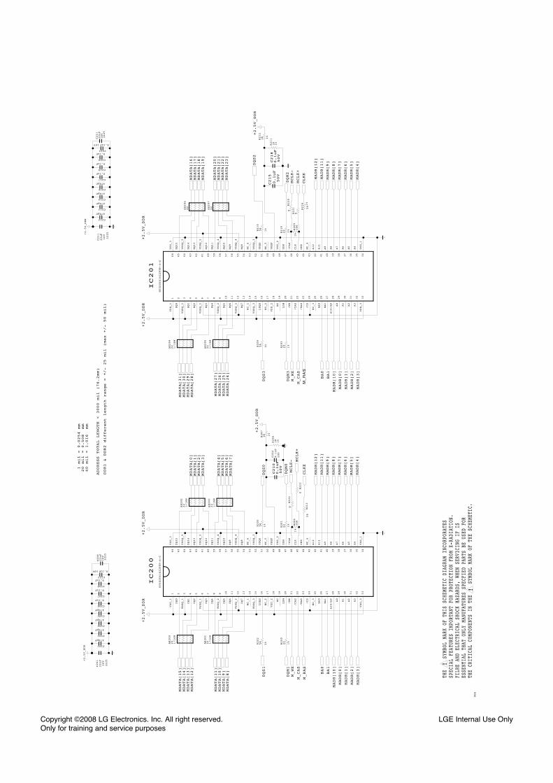
THE
S
YMBO
L MA
RK O
F TH
IS S
CHEM
ETIC
DIA
GRAM
INC
ORPO
RATE
SSP
ECIA
L FE
ATUR
ES I
MPOR
TANT
FOR
PRO
TECT
ION
FROM
X-R
ADIA
TION
.FI
LRE
AND
ELEC
TRIC
AL S
HOCK
HAZ
ARDS
, WH
EN S
ERVI
CING
IF
IS
ESSE
NTIA
L TH
AT O
NLY
MANU
FATU
RES
SPEC
FIED
PAR
TS B
E US
ED F
ORTH
E CR
ITIC
AL C
OMPO
NENT
S IN
THE
SYMB
OL M
ARK
OF T
HE S
CHEM
ETIC
.DDR
MADR[6]
MDATA[3]
C208
0.1uF
MDATA[5]
MADR[8]
MADR[11]
C209
22uF
16V
3225
C206
0.1uF
MDATA[9]
MDATA[12]
MDATA[0]
MADR[9]
BA0
M_RAS
MDATA[11]
MADR[10]
MDATA[13]
C210
0.1uF
50V
DQS0
C207
0.1uF
+2.5V_DDR
M_CAS
MADR[4]
MADR[2]
+2.5V_DDR
MADR[12]
MADR[1]
MADR[5]
R206
1K
1%
MDATA[2]
MDATA[8]
+2.5V_DDR
MADR[0]
MADR[3]
MDATA[1]
MADR[7]
+2.5V_DDR
M_WE
BA1
MDATA[4]
MDATA[10]
R207
1K 1%
MADR[7]
MADR[11]
MADR[12]
DQS2
MDATA[18]C220
0.1uF
BA1
+2.5V_DDR
C219
0.1uF
MDATA[17]
+2.5V_DDR
MDATA[27]
MDATA[19]
MDATA[26]
MDATA[28]
MADR[8]
MADR[10]
DQS3
MADR[2]
MDATA[29]
MADR[5]
C217
0.1uF
MADR[6]
MDATA[25]
MADR[3]
R212
1K 1%
C218
0.1uF
50V
M_
RA
S
+2.5V_DDR
M_CAS
R211
1K
1%
MADR[0]
MADR[4]
MADR[1]
M_WE
MDATA[16]
BA0
MADR[9]
MDATA[24]
+2.5V_DDR
AR200
22
1/16W
AR201
22
1/16W
AR202
22
1/16W
AR203
22
1/16W
AR204
22
1/16W
AR205
22
1/16W
AR207
22
AR206
22
DQS1
DQM1
MDATA[14]
MDATA[15]
R200
22
1%
DQM0
MDATA[7]
MDATA[6]
R201
22 1%
CLKE
MCLK+
MCLK-
C221
22uF
16V
3225
MDATA[30]
DQM3
C222
0.1uF50V
C224
0.1uF
50V
MDATA[31]
R203
22
1%
CLKE
DQM2
MCLK-
MCLK+
MDATA[21]
MDATA[23]
MDATA[20]
MDATA[22]
R219
22 1%
C201
22uF
16V
3225
C211
22uF
16V
3225
IC201
HY5DU561622FTP-4-C
26
BA0
27
BA1
28
A10/AP
29
A0
30
A1
31
A2
32
A3
33
VDD_3
34
VSS_1
35
A4
36
A5
37
A6
38
A7
39
A8
40
A9
41
A11
42
A12
43
NC_4
44
CKE
45
CLK
46
/CLK
47
UDM
48
VSS_2
49
VREF
50
NC_5
17
NC_2
3VDDQ_1
6VSSQ_1
16
LDQS
15
VDDQ_3
14
NC_1
13
DQ7
12
VSSQ_2
11
DQ6
10
DQ5
9VDDQ_2
8DQ4
7DQ3
4DQ1
5DQ2
25
NC_3
24
/CS
23
/RAS
2DQ0
22
/CAS
21
/WE
1VDD_1
20
LDM
19
NC
18
VDD_2
51
UDQS
52
VSSQ_3
53
NC_6
54
DQ8
55
VDDQ_4
56
DQ9
57
DQ10
58
VSSQ_4
59
DQ11
60
DQ12
61
VDDQ_5
62
DQ13
63
DQ14
64
VSSQ_5
65
DQ15
66
VSS_3
IC200
HY5DU561622FTP-4-C
26
BA0
27
BA1
28
A10/AP
29
A0
30
A1
31
A2
32
A3
33
VDD_3
34
VSS_1
35
A4
36
A5
37
A6
38
A7
39
A8
40
A9
41
A11
42
A12
43
NC_4
44
CKE
45
CLK
46
/CLK
47
UDM
48
VSS_2
49
VREF
50
NC_5
17
NC_2
3VDDQ_1
6VSSQ_1
16
LDQS
15
VDDQ_3
14
NC_1
13
DQ7
12
VSSQ_2
11
DQ6
10
DQ5
9VDDQ_2
8DQ4
7DQ3
4DQ1
5DQ2
25
NC_3
24
/CS
23
/RAS
2DQ0
22
/CAS
21
/WE
1VDD_1
20
LDM
19
NC
18
VDD_2
51
UDQS
52
VSSQ_3
53
NC_6
54
DQ8
55
VDDQ_4
56
DQ9
57
DQ10
58
VSSQ_4
59
DQ11
60
DQ12
61
VDDQ_5
62
DQ13
63
DQ14
64
VSSQ_5
65
DQ15
66
VSS_3
C215
0.1uF
50V
C202
470pF
C203
470pF
C204
470pF
C205
470pF
C212
470pF
C213
470pF
C214
470pF
C216
470pF
R220
0
R221
0
R222
0
R223
0
C223
0.1uF16V
R208
56
1%
R216
561%
R213
56
R202
56
1%
R205
56
1% R204
300
1%
R209
300
1%
R210
56
1%
ADDRESS TOTAL LENGTH < 3000 mil (76.2mm)
DDR1 & DDR2 different length range = +/- 25 mil (max +/- 50 mil)
1 mil = 0.0254 mm
20 mil = 0.508 mm
40 mil = 1.016 mm
Copyright ©2008 LG Electronics. Inc. All right reserved. Only for training and service purposes
LGE Internal Use Only

THE
S
YMBO
L MA
RK O
F TH
IS S
CHEM
ETIC
DIA
GRAM
INC
ORPO
RATE
SSP
ECIA
L FE
ATUR
ES I
MPOR
TANT
FOR
PRO
TECT
ION
FROM
X-R
ADIA
TION
.FI
LRE
AND
ELEC
TRIC
AL S
HOCK
HAZ
ARDS
, WH
EN S
ERVI
CING
IF
IS
ESSE
NTIA
L TH
AT O
NLY
MANU
FATU
RES
SPEC
FIED
PAR
TS B
E US
ED F
ORTH
E CR
ITIC
AL C
OMPO
NENT
S IN
THE
SYMB
OL M
ARK
OF T
HE S
CHEM
ETIC
.MODUEL&CTL
LVA_0M
LVB_2P
+3.3V_CI
C302
1000pF
50V
EN_1.3VF
R307
4.7K
FHD&NON-FRC
L302
FRC
LVA_CKP
EN_3.3VF
LVB_0M
LVA_3M
LVA_3P
L301
FRC
R310
1.3K
BIT_SEL
P301
SMAW200-40C
FHD_LVDS_wafer
1 2 3 4 5 6 7 8 9
10
11
12
13
14
15
16
17
18
19
20
21
22
23
24
25
26
27
28
29
30
31
32
33
34
35
36
37
38
39
40
+5V_
GENE
RAL
C301
0.1uF
50V
LVB_4M
L303
FRC
R309
0OPT
+3.3V_CI
EN_1.3PLL
P302
SMAW200-26C
HD
1 2 3 4 5 6 7 8 9
10
11
12
13
14
15
16
17
18
19
20
21
22
23
24
25
26
LVB_CKP
R313
1.3K
LVA_4P
+3.3
V_VD
DP_S
T
LVB_3P
+12V
R311
1.3K
LVA_0P
LVB_1M
R306
4.7K
NON-FRC
LVB_3M
LVB_2M
+3.3V_CI
FRC_RESET
P303
SMAW200-13
FRC
1 2 3 4 5 6 7 8 9
10
11
12
13
LVA_CKM
LVB_0P
R305
0
OPT
LVA_4M
R308
0OPT
LVDS_SEL
LVB_CKM
R302
0OPT
R303
0
HD
EN_2.5VF
LVA_2P
+15V
LVB_4P
LVA_2M
PANEL_POWER
003:T8;009:K5
EN_1.8VF
LVA_1P
L304
OPT
LVA_1M
R301
0FRC
R312
1.3K
R304
0OPT
LVB_1P
R314
0OPT
SDA_D_TU
R316
0FRC
SCL_D_TU
R315
0FRC
PANEL_POWER
003:L19;009:K5
+3.3V_CI
R11890
OPT
R11900
OPT
R11910
OPT
R1192
0OPT
JP3007
JP3006
JP3005
JP3001
JP3002
JP3003
JP3004
FRAME_SEL
R317
0OPT
JP3008
C303
100uF
16V
PANEL_POWER DEVIDER
Copyright ©2008 LG Electronics. Inc. All right reserved. Only for training and service purposes
LGE Internal Use Only
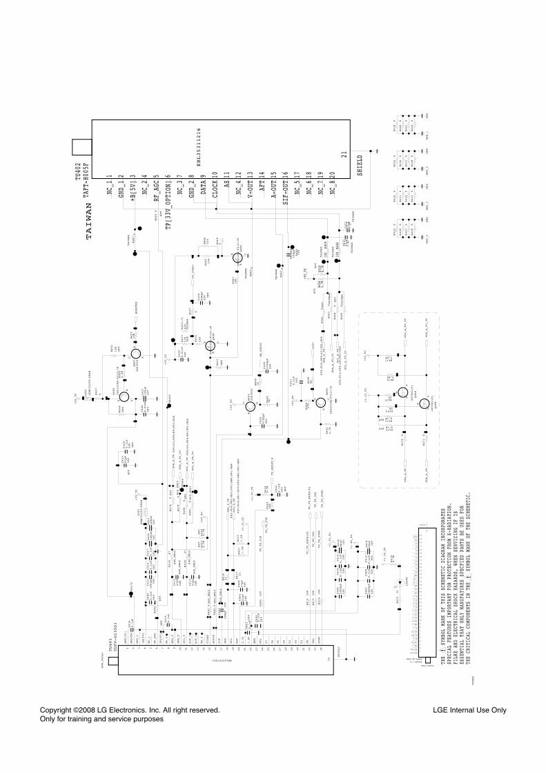
THE
S
YMBO
L MA
RK O
F TH
IS S
CHEM
ETIC
DIA
GRAM
INC
ORPO
RATE
SSP
ECIA
L FE
ATUR
ES I
MPOR
TANT
FOR
PRO
TECT
ION
FROM
X-R
ADIA
TION
.FI
LRE
AND
ELEC
TRIC
AL S
HOCK
HAZ
ARDS
, WH
EN S
ERVI
CING
IF
IS
ESSE
NTIA
L TH
AT O
NLY
MANU
FATU
RES
SPEC
FIED
PAR
TS B
E US
ED F
ORTH
E CR
ITIC
AL C
OMPO
NENT
S IN
THE
SYMB
OL M
ARK
OF T
HE S
CHEM
ETIC
.TUNER
TU_TS_SYNC
TU_TS_VAL
TU_TS_DATA[0]
TU_TS_CLK
C416
0.1uF
50V
+3.3V_TU
R415
33
C408
47pF
50V
C404
47pF
50V
SDA_D_TU
003:M14;001:H25;001:AB6;001:AM6
SCL_D_TU
003:M14;001:H25;001:AB5;001:AM5
+3.3V_TU
L401
LEMC3225T-6R8M
C421
100uF
16V
C420
100uF
16V
C417
0.1uF
50V
C414
0.1uF
50V
C405
0.1uF
50V
+5V_TU
BOOSTER
+5V_TU
R450
2.2K
R455
10K
C427
100uF
16V
C426
0.01uF
50V
R444
OPT
L402
LEMC3225T-6R8M
Q405
2SA1530A-T112-1R
E
B
C
R402
0
OPT
C423
47pF
50V
OPT
R401
0AUS_ONLY
R451
OPT
Q404
2SA1530A-T112-1R
E
B
C
C429
0.01uF
50V
R454
220
Q406
2SA1530A-T112-1R
E
B
C
R468
0
TV_CVBS+
+5V_TU
C403
100pF
50VAUS_ONLY
R443
4.7K
Q403
2SA1530A-T112-1R
E
B
C
R446
470
R449
82
SIF+
+5V_TU
C413
47pF
50V
AUS_ONLY
C412
47pF
50V
AUS_ONLY
R420
47
AUS_ONLY
R419
47
AUS_ONLY
+3.3V_TU
R422
4.7K
OPT
R424
4.7K
OPT
+5V_TU
C402
0.1uF
50V
C401
0.1uF50V
+1.8V_TU
C419
100uF
16V
C410
0.1uF
50V
C415
0.1uF
50V
C409
0.1uF
50V
C418
100uF
16V
R441
0
R442
0
R440
0
R439
0
GND_1
R435
0
R437
0
R438
0
GND_2R436
0
R430
0
R432
0
R433
0
GND_3R431
0
R425
0
R427
0
R428
0
GND_4R426
0
SCL_A_TU
004:L4;004:R8;001:H26
GND
GND
GND
GND
R452
10K
OPT
+5V_TU
R403
0AUS_ONLY
C425
4700pF
50V
R445
1K
R448
1K
C428
4700pF
50V
TU_RESET_N
R429
100
+3.3V_TU
R418
4.7K
C411
1000pF
50V
C406
1000pF
50V
C407
1000pF
50V
R434
4.7K
R457
0
C422
0.1uF
50V
OPT
R465
330
R447
0
R461
100
R466
330
Q402
2SC3052
E
B
C
Q407
2SC3052
E
B
C
C424
0.1uF
50V
OPT
LD400
TU401
TDFV-G135D1
AUS_Tuner
EBL42367001
1ANT[5V]
2BB[CTR]
3GND_1
4+B[5V]
5NC_1
6RF_AGC
7TP[VT]
8NC_2
9GND_2
10
SDA_T
11
SCL_T
12
AIF_1
13
AIF_2
14
NC_3
15
VIDEO
16
AUDIO
17
SIF
18
SDA
19
SCL
20
RST
21
3.3V
22
1.8V
23
ERR
24
MCL
25
D7
26
D6
27
D5
28
D4
29
D3
30
D2
31
D1
35
SHIELD
32
D0
33
VAL
34
SYNC
R416
33 R417
33
R421
1.2K
R423
1.2K
R4620
TAIWAN
R4630
TAIWAN
R4670
TAIWAN
R469
0
OPT
C432
27pFTAIWAN
+5V_
TU R458
4.7KOPT
C431
27pF
TAIWAN
R456
4.7K
OPT
SDA_A_TU
004:K16;004:L3;001:H26
SCL_A_TU
004:K15;004:L4;001:H26
TU_TS_DATA[0]
TU_TS_VAL
TU_TS_SYNC
TU_TS_CLK
R4724.7KOPT
SCL_A_TU
Q408
2N7002(F)
G
D
S
Q409
2N7002(F)
G
D
S+3.3V_TU
R471
0
SCL_A_TU_5V
SDA_A_TU
+5V_TU
SDA_A_TU_5V
R4742K
R4752K
R4775.6K
R470
0
R4765.6K
R4734.7KOPT
R481
0AUS_ONLY
R480
0OPT
SCL_A_TU_5V
SDA_A_TU_5V
R479
0AUS_ONLY
R478
0OPT
SDA_A_TU
004:L3;004:R8;001:H26
R483
0TAIWAN
SCL_A_TU_5V
R484
0OPT
R485
0TAIWAN
R482
0OPT
SDA_A_TU_5V
C433
0.1uF
16V
R464
100pF
TAIWAN
50V
R459
100
TAIWAN R460
100
TAIWAN
TU40
2TA
FT-H
005F
TAIWAN
EBL35311216
14AF
T
13V-
OUT
5RF
_AGC
12NC
_4
11AS
2GN
D_1
19NC
_7
18NC
_6
10CL
OCK
4NC
_2
1NC
_1
17NC
_5
9DA
TA
8GN
D_2
3+B
[5V]
16SI
F-OU
T
7NC
_3
6TP
[33V
_OPT
ION]
15A-
OUT
21
SHIE
LD
20NC
_8
TP465
TP466
TP470
R412
100
R413
100
R414
100
R404
100
TU401-*1
TDFV-D135F
TAIWAN_TUNER
1ANT[5V]
2BB[CTR]
3GND_1
4+B[5V]
5NC_1
6RF_AGC
7TP[VT]
8NC_2
9GND_2
10SDA_T
11SCL_T
12AIF_1
13AIF_2
14NC_3
15NC_4
16NC_5
17NC_6
18SDA
19SCL
20RST
213.3V
221.8V
23ERR
24MCL
25D7
26D6
27D5
28D4
29D3
30D2
31D1
35
SHIELD
32D0
33VAL
34SYNC
C434
0.1uF
C435
0.1uF
OPT
R453-*1
220
TAIWAN
R453
270
AUS
C430
680pF
50V OPT
AM_AUDIO
Copyright ©2008 LG Electronics. Inc. All right reserved. Only for training and service purposes
LGE Internal Use Only

THE
S
YMBO
L MA
RK O
F TH
IS S
CHEM
ETIC
DIA
GRAM
INC
ORPO
RATE
SSP
ECIA
L FE
ATUR
ES I
MPOR
TANT
FOR
PRO
TECT
ION
FROM
X-R
ADIA
TION
.FI
LRE
AND
ELEC
TRIC
AL S
HOCK
HAZ
ARDS
, WH
EN S
ERVI
CING
IF
IS
ESSE
NTIA
L TH
AT O
NLY
MANU
FATU
RES
SPEC
FIED
PAR
TS B
E US
ED F
ORTH
E CR
ITIC
AL C
OMPO
NENT
S IN
THE
SYMB
OL M
ARK
OF T
HE S
CHEM
ETIC
.
COMP1_Pr
005:T6
R505
0
L501
MBW3216-501TF
COMP1_Pb
005:T6
R522
22
R506
0R524
22
R523
22
R502
0 R504
0
R5120
R503
0
COMP1_Y
005:T7
COMP_Pb
001:F18
IC500
STMAV340
EAN32724702
32B
21C
42C
11B
63C
53B
74B
84C
9GND
10
4A
11
3A
12
2A
13
1A
14
S
15
OE_N
16
VCC
C506
0.01uF
COMP2_Pr
005:J7
C507
47uF
16V
COMP_Pr
001:F18
+5V_GENERAL
R507
0R525
22
COMP_Y
001:F18
COMP_SEL
008:E6;008:O10;001:H24
COMP2_Pb
005:J8
COMP2_Y
005:J9
COMP2_Pr
C508
0.1uF
50V
R537
10K
R532
470K
D506
5.6V
CDS3C05GTA
OPT
COMP1_R_IN
R511
75
R516
22
D510
5.6V
CDS3C05GTA
OPT
R514
470K
COMP1_DET
001:W4
R513
470K
R501
10K
D503
30V
CDS3C30GTH
OPT
R533
22
D501
30V
CDS3C30GTH
OPT
D512
5.6V
CDS3C05GTA
OPT
C512
100pF
50V
COMP1_Pb
R508
1K
R528
75
D507
30V
CDS3C30GTH
OPT
COMP2_DET
001:W4
R526
10K
+5V_GENERAL
R509
75
D505
5.6V
CDS3C05GTA
OPT
D502
30V
CDS3C30GTH
OPT
R517
22
D504
5.6V
CDS3C05GTA
OPT
C504
100pF
50V
R521
12K
C505
100pF
50V
D509
30V
CDS3C30GTH
OPT
R515
22
JK501
PPJ209-02
6612J10031A
4A
[GN]CONTACT
2A
[GN]1P_CAN
3A
[GN]O_SPRING
2B
[BL]1P_CAN
5B
[BL]C_LUG_L
2C
[RD]1P_CAN1
5C
[RD]C_LUG_L
2D
[WH]1P_CAN
5D
[WH]C_LUG_L
2E
[RD]1P_CAN2
4E
[RD]CONTACT
3E
[RD]O_SPRING
R520
12K
R530
75
R529
75
R510
75
C511
100pF
50V
C503
0.1uF
50V
R536
10K
COMP1_Pr
D508
30V
CDS3C30GTH
OPT
COMP2_R_IN
R538
12K
C510
0.1uF
50V
COMP2_Y
R539
12K
COMP1_L_IN
R534
22
C509
0.1uF
50V
R531
470K
COMP2_L_IN
C501
0.1uF
50V
R518
10K
D511
5.6V
CDS3C05GTA
OPT
C502
0.1uF
50V
R535
22
+5V_GENERAL
JK502
PPJ209-02
6612J10031A
4A
[GN]CONTACT
2A
[GN]1P_CAN
3A
[GN]O_SPRING
2B
[BL]1P_CAN
5B
[BL]C_LUG_L
2C
[RD]1P_CAN1
5C
[RD]C_LUG_L
2D
[WH]1P_CAN
5D
[WH]C_LUG_L
2E
[RD]1P_CAN2
4E
[RD]CONTACT
3E
[RD]O_SPRING
R527
1K
R519
10K
COMP1_Y
COMP2_Pb
D520
5.6V
CDS3C05GTA
OPT
JP5015
R548
75
D517
30V
CDS3C30GTH
R543
22
C517
OPT
OPT
P501
KCN-DS-1-0089
1
2
3
4
5
6
7
8
9
10
11
12
13
14
15
16
D513
30V
EEPROM_WP
DSUB_HSYNC
JP5013
+5V_GENERAL
JP5017
R552
22
D519
ENKMC2838-T112
A1
C
A2
C518
0.1uF
50V
R557
10K
R551
4.7K
R556
100
JP5014
DSUB_B
C516
OPT
OPT
R546
75
R544
22
C520
18pF
50V
DSUB_G
JP5016
C519
18pF
50V
R553
10K
D521
5.6V
CDS3C05GTA
OPT
DSUB_R
R550
4.7K
IC501
AT24C02BN-10SU-1.8
0IMMRAL014D
3A2
2A1
4GND
1A0
5SDA
6SCL
7WP
8VCC
D516
30V
CDS3C30GTH
R555
0 OPT
D518
5.6V
CDS3C05GTA
OPT
DSUB_DET
C514
22pF
50V
R542
10K
DDC_SCL/UART_RX
D515
30V
CDS3C30GTH
R547
75
D514
30V
CDS3C30GTH
DSUB_VSYNC
C515
OPT
OPT
R545
22
R558
1K
DDC_SDA/UART_TX
R541
100
R549
10K
C513
22pF
50V
R554
22
R540
100
R7017
100
R7018
100
+5V_ST
JP5020
JP5021
TP551
HIGH:COMP1
COMPONENT-SW
LOW :COMP2
COMPONENT1
COMPONENT2
D-SUB
Copyright ©2008 LG Electronics. Inc. All right reserved. Only for training and service purposes
LGE Internal Use Only

USB DOWN STREAM
THE
S
YMBO
L MA
RK O
F TH
IS S
CHEM
ETIC
DIA
GRAM
INC
ORPO
RATE
SSP
ECIA
L FE
ATUR
ES I
MPOR
TANT
FOR
PRO
TECT
ION
FROM
X-R
ADIA
TION
.FI
LRE
AND
ELEC
TRIC
AL S
HOCK
HAZ
ARDS
, WH
EN S
ERVI
CING
IF
IS
ESSE
NTIA
L TH
AT O
NLY
MANU
FATU
RES
SPEC
FIED
PAR
TS B
E US
ED F
ORTH
E CR
ITIC
AL C
OMPO
NENT
S IN
THE
SYMB
OL M
ARK
OF T
HE S
CHEM
ETIC
.
+12V_AVOUT
R628
100
R624
4.7K
D605
5.6V
CDS3C05GTA
OPT
R629
0
R623
4.7K
RS232C_TXD
001:H29
+3.3V_VDDP_ST
C603
100pF
50V
+3.3V_VDDP_ST
C602
100pF
50V
JK603
PEJ024-01
6612F00099A6B
T_TERMINAL2
8SHIELD_PLATE
7B
B_TERMINAL2
5T_SPRING
4R_SPRING
7A
B_TERMINAL1
6A
T_TERMINAL1
3E_SPRING
PC_R_IN
001:G15
RS232C_RXD
R626
100
D604
5.6V
CDS3C05GTA
OPT
D611
30V
CDS3C30GTH
OPT
D610
30V
CDS3C30GTH
OPT
R603
470K R608
470K
PC_L_IN
001:G15
C617
0.47uF
25V
R613
10K
R612
10K
D612
5.6V
OPT
+5V_USB
D613
5.6V
OPT
C62210uF16V
USB_DM
TP619
TP620
TP621
USB_DP
L606
MBW3216-501TF
P601
KCN-DS-1-0088
1
2
3
4
5
6
7
8
9
10
R615
5.1K
R616
5.1K
IC601
MAX3232CDR
EAN41348201
3C1-
2V+
4C2+
1C1+
6V-
5C2-
7DOUT2
8RIN2
9ROUT2
10DIN2
11DIN1
12ROUT1
13RIN1
14DOUT1
15GND
16VCC
R635
51K
R636
100K
JK606
PPJ200-07
3A
2A
4A
2B
5B
JP6018
ZD602OPT
JP6019
ZD601
OPT
JK604
PPJ204-01
EAG35542201
1O_SPRING
2CONTACT
3U_CAN
SIDE_C_IN
D607
30V
CDS3C30GTH
+5V_GENERAL
R610
1K
R619
75
SIDE_CVBS_IN
D609
30V
C608
100pF
50V
OPT
SIDE_Y_IN
R611
22
L603
D608
30V
CDS3C30GTH
D606
30V
CDS3C30GTH
L601
SIDE_Y/C_DET
C604
100pF
50V
C605
100pF
50V
R61422
R617
10K
R601
10K
C607
100pF
50V
OPT
R607
75
C601
0.1uF
16V
+5V_GENERAL
R604
470K
R602
10K
L602
R621
12K
SIDE_CVBS_DET
R606
75
SIDE_L_IN
C606
100pF
50V
OPT
SIDE_R_IN
R622
12K
R605
470K
R609
22
R618
10KR620
0
Q604
2SA1530A-T112-1R
E
B
C
R638
1.5K
Q603
2SA1530A-T112-1R
E
B
C
L609
BG2012B080TF
R639
1K
C627
0.1uF
16V
C632
10uF
AV_L_OUT
R641
1K
R646
47K
R643
47K
Q605
2SC3875S
E
B
C
+12V_AVOUT
006:X19;006:AE16
Q606
2SC3875S
E
B
C
C623
1000pF
50V
C633
0.1uF
16V
OPT
C635
OPT
C625
1000pF
50V
R647
15K
L608
BG2012B080TF
C626
0.1uF
16V
C631
10uF
6.3V
R637
1.5K
D614
5.6V
OPT
R644
15K
AV_R_OUT
D615
5.6V
OPT
R627
75
C615
100uF
16V
+12V_AVOUT
006:AE16;006:AI12
R633
47K
C614
100uF
16V
R630
680
C620
47uF
16V
R634
15K
Q602
2SC3875S
E
B
C
R632
470
C621
0.1uF
50V
Q601
2SA1530A-T112-1R
E
B
C
AV_CVBS_OUT
R649
2K
+12V_AVOUT
006:X19;006:AI12
C630
0.1uF
50V
L610
HH-1M3216-501
+12V
003:Z14;008:Z12;009:A8;009:F12;009:H19
P602KJA-UB-4-0004
1 2 3 45
JK602
PSJ018-01
EAG42206001
1GND_TER
2C_LUG_S1
3C_LUG_L1
6NC1
7COM1
8NO1
9NC2
10
COM2
11
NO2
12 SHIELD
4C_LUG_S2
5C_LUG_L2
JK601
PPJ218-01
EAG422058015C
[RD]CONTACT
2C
[RD]U_CAN
4C
[RD]O_SPRING
2B
[WH]U_CAN
3B
[WH]C_LUG
2A
[YL]U_CAN
5A
[YL]CONTACT
4A
[YL]O_SPRING
C618470pF
C619470pF
C610
0.1uF
50V
C612
0.1uF
50V
C613
0.1uF
50V
C616
0.1uF
50V
C609
220pF
50V
C611
220pF
50V
USB_CTL
001:H28
R645
560K
R651
100K
OPT
C634
0.1uF
50V
+5V_USB
+5V
USB_OCD
001:AB4
R650
10K
R625
0OPT
JP6017
JP6020
JP6021
JP6023
JP6022
C629
100uF
16V
Q607
2SC3875S
E
B
C
Q608
2SC3875S
E
B
C
MUTE_AV_L/R
001:H27
R648
2K
TP660
TP664
TP665
TP666
TP667IC602
TPS2042ADRG4
3EN1
2IN
4EN2
1GND
5OC2
6OUT2
7OUT1
8OC1
ZD606
5.6B
ZD603
5.6B
ZD604
5.6B
ZD607
5.6B
ZD605
5.6B
ZD608
5.6B
C628
4.7uF
35V
C624
4.7uF
35V
+3.3V_VDDP_ST
R6524.7K
L605
2.2uH
L604
2.2uH
R642
560
R640
560
R631-*1
200
TAIWAN
R631
220
AUS
RS232C
USB
PC-AUDIO
Monitor Out - CVBS
AV-OUT-AUDIO
AV-OUT-CVBS
Side AV
Copyright ©2008 LG Electronics. Inc. All right reserved. Only for training and service purposes
LGE Internal Use Only
THE
S
YMBO
L MA
RK O
F TH
IS S
CHEM
ETIC
DIA
GRAM
INC
ORPO
RATE
SSP
ECIA
L FE
ATUR
ES I
MPOR
TANT
FOR
PRO
TECT
ION
FROM
X-R
ADIA
TION
.FI
LRE
AND
ELEC
TRIC
AL S
HOCK
HAZ
ARDS
, WH
EN S
ERVI
CING
IF
IS
ESSE
NTIA
L TH
AT O
NLY
MANU
FATU
RES
SPEC
FIED
PAR
TS B
E US
ED F
ORTH
E CR
ITIC
AL C
OMPO
NENT
S IN
THE
SYMB
OL M
ARK
OF T
HE S
CHEM
ETIC
.HDMI
D2+_HDMI3
CK+_HDMI4
HDMI_SCL
R747
0
OPT
R70030
HPD4
R749
0 OPT
R725
47K
HPD3
R732
22
OPT
R7810
+3.3V_VDDP_ST
HPD1
DDC_SCL_4
007:V9;007:AE24
CK+_HDMI1
R718
0
OPT
DDC_SCL_1
C711
0.1uF
C718
0.1uF
R7790
R708
0
R7944.7K OPT
EEPROM_WP
D0-_HDMI4
DDC_SDA_4
D2+_HDMI4
+3.3V_HDMI_ST
D2+_HDMI2
R750
0 OPT
R762
4.7K
OPT
+3.3V_VDDP_ST
HDMI_CLK+
R797
4.7K
R7007
36K
OPT
+5V_ST
R702
3.6K
GND
R703
1K
+5V_ST
+5V_ST
C707
0.1uF
Q703
2SC3052
E
B
C
+3.3V_VDDP_ST
R731
22
OPT
CK+_HDMI2
GND
R705
1K
C720
0.1uF
CK+_HDMI1
5V_HDMI_1
R745
0
R756
22
OPT
5V_HDMI_4
D1+_HDMI3
C705
0.1uF
D2-_HDMI2
R7740OPT
R728
0 OPT
R7900
IC702
AT24C02BN-10SU-1.8
OPT
3A2
2A1
4GND
1A0
5SDA
6SCL
7WP
8VCC
R755
22
OPT
D2+_HDMI2
R701
3.6K
5V_HDMI_1
R784
100
OPT
C704
0.1uF
R7680
HDMI_RX0-
DDC_SCL_3
Q704
2SC3052
E
B
C
R740
0
OPT
R7720
R741
3.6K
D2-_HDMI1
HDMI_CEC
001:J20;007:AF11
CK-_HDMI4
HPD
CK-_HDMI2
R7800
D1+_HDMI1
D1-_HDMI1
R743
27K
R7005
36K
OPT
R7006
0
D2+_HDMI1
R709
0
DDC_SCL_1
R7880
OPT
D2-_HDMI4
R730
22
OPT
R766
0
DDC_SDA_3
R710
0
CK-_HDMI1
CK+_HDMI3
D705
ENKMC2838-T112
A1
C
A2
DDC_SCL_3
R714
0
C716
0.1uF
R746
0
DDC_SDA_1
5V_HDMI_2
D1+_HDMI4
+3.3V_VDDP_ST
5V_HDMI_2
HDMI_RX0+
IC703
AT24C02BN-10SU-1.8
OPT
3A2
2A1
4GND
1A0
5SDA
6SCL
7WP
8VCC
D2-_HDMI3
D701
ENKMC2838-T112
A1
C
A2
D0+_HDMI2
BSS83
Q705
SB
D
G
D0-_HDMI1
CK-_HDMI3
DDC_SCL_2
C709
0.1uF
DDC_SDA_3
DDC_SCL_2
R729
0 OPT
D1-_HDMI4
R7440
OPT
R7910
HDMI_CEC
GND
R727
47K
PS421/NTP_SDA
008:H15;001:H24
D702
ENKMC2838-T112
A1
C
A2
R711
0
R706
1K
CK+_HDMI3 SDA_EYEQ/AMP
Q701
2SC3052
E
B
C
R713
0
D0+_HDMI4
R716
0
OPT
D0-_HDMI2
D0+_HDMI1
C701
0.1uF
50V
HPD2
PS421/NTP_SCL
R765
36K
OPT
D1-_HDMI2
R742
1K
DDC_SCL_2
007:H17;007:AJ9
D0-_HDMI2
EEPROM_WP
CEC_REMOTE
007:F26;007:F17;007:O16;007:T8
D704
MMBD301LT1G
30V
AC
D1+_HDMI2
CK-_HDMI4
D0+_HDMI1
DDC_SCL_3
EEPROM_WP
CK-_HDMI3
5V_HDMI_3
001:H24;007:O23;007:AD13
D0-_HDMI3
D1+_HDMI1
HDMI_RX2-
GND
C712
0.1uF
R783
100
OPT
CEC_REMOTE
DDC_SDA_2
CEC_REMOTE
007:F8;007:F26;007:F17;007:T8
R7730
D0-_HDMI3
D1+_HDMI4
HDMI_RX2+
R707
0
R764
0
HPD1
CK-_HDMI2
R7750
OPT
D0-_HDMI1
D0-_HDMI4R753
22
OPT
R704
3.6K
D706
ENKMC2838-T112
A1
C
A2
HPD2
DDC_SDA_4
R7964.7KOPT
5V_HDMI_4
DDC_SCL_1
R7710
5V_HDMI_3
D2-_HDMI2
R754
22
OPT
DDC_SCL_4
D1-_HDMI3
DDC_SDA_1
HDMI_RX1+
DDC_SCL_4
DDC_SDA_4
+5V_ST
R7008
0
R719
0
OPT
CK+_HDMI2
R7700
5V_HDMI_3
R795510
HPD4
HDMI_RX1-
R761
4.7K
OPT
Q702
2SC3052
E
B
C
R715
0
C702
0.1uF
50V
R7764.7K
OPT
D2+_HDMI4
R7690
D2+_HDMI3
D1-_HDMI2
R7920
C7152.2uF
R70010
R7890
OPT
R712
0
R787 0OPT
R737
68K
R7980
5V_HDMI_2
001:H23;007:W29;007:AM11
+3.3V_VDDP_ST
D1-_HDMI1
C706
0.1uF
50V
GND
D0+_HDMI4
D1+_HDMI2
CK-_HDMI1
DDC_SDA_3
HDMI_CLK-
C710
0.1uF
C714
0.1uF
HPD3
007:AF11
R738 0
OPT
D1+_HDMI3
D2-_HDMI4
IC701
AT24C02BN-10SU-1.8
OPT
3A2
2A1
4GND
1A0
5SDA
6SCL
7WP
8VCC
D0+_HDMI2
R70020
EEPROM_WP
D703
OPT
D1-_HDMI3
C717
0.1uF
5V_HDMI_1
001:H23;007:O28;007:AK25
SCL_EYEQ/AMP
CEC_REMOTE
R763
36K
OPT
CEC_REMOTE
D0+_HDMI3
R7860
OPT
D1-_HDMI4
R70040
D2-_HDMI3
D0+_HDMI3
D2-_HDMI1
GND
C703
0.1uF
50V
D2+_HDMI1
R767
4.7K
OPT
R733
22
OPT
DDC_SDA_2
R752
47K
R723
47K
IC704
AT24C02BN-10SU-1.8
OPT
3A2
2A1
4GND
1A0
5SDA
6SCL
7WP
8VCC
DDC_SDA_2
HDMI_SDA
JK704
DC1R019NBH
EAG42025501
14
NC
13
CEC
5DATA1_SHIELD
20
JACK_GND
12
CLK-
11
CLK_SHIELD
2DATA2_SHIELD
19
HPD
18
+5V_POWER
10
CLK+
4DATA1+
1DATA2+
17
DDC/CEC_GND
9DATA0-
8DATA0_SHIELD
3DATA2-
16
SDA
7DATA0+
6DATA1-
15
SCL
DDC_SDA_1
C719
0.1uF
R7990
CK+_HDMI4
5V_HDMI_4
C713
0.1uF
C708
0.1uF
R722 1K
R724 1KR726 1K
R751 1K
JK702
EAG39789401
1D2+
2D2_GND
3D2-
4D1+
5D1_GND
6D1-
7D0+
8D0_GND
9D0-
10
CK+
11
12
13
14
15
16
17
18
19
20
GND
21
GND
22
JK701
EAG39789401
1D2+
2D2_GND
3D2-
4D1+
5D1_GND
6D1-
7D0+
8D0_GND
9D0-
10
CK+
11
12
13
14
15
16
17
18
19
20
GND
21
GND
22
JK703
EAG39789401
1D2+
2D2_GND
3D2-
4D1+
5D1_GND
6D1-
7D0+
8D0_GND
9D0-
10
CK+
11
12
13
14
15
16
17
18
19
20
GND
21
GND
22
R7009 0
R7010 0
OPT
+3.3V_CI
R777
3.3K
R778
3.3K
JP7010
JP7009
JP7003
JP7004
JP7005
JP7006
JP7002
JP7001
JP7007
JP7008
JP7012
JP7011
R735
10K
R739
10K
R757
10K
R758
10K
R759
10K
R734
10K
R760
10K
R736
10K
R7850
R70110
IC705
PS421
1 SCL1
2 SDA1
3 GPD1
4 POW1
5 CEC
6 DDCBUF_EN
7 GND_1
8 CEXT
9 PC0/I2C_RST
10 PC1/I2C_ADDR1
11 TEST
12 VCC_1
13 ECE_IN
14 CEC_OUT
15 S1/SDA_CTL
16 S2/SCL_CTL
17 S3/I2C_ADDR0
18 OE#/POWDN
19 I2C_CTL_EN
20 REXT
21 GND_2
22 POW4
23 HPD4
24 SDA4
25 SCL4
26
GND_3
27
IN4D1N
28
IN4D1P
29
VCC_2
30
IN4D2N
31
IN4D2P
32
GND_4
33
IN4D3N
34
IN4D3P
35
VCC_3
36
IN4D4N
37
IN4D4P
38
GND_5
39
IN3D1N
40
IN3D1P
41
VCC_4
42
IN3D2N
43
IN3D2P
44
GND_6
45
IN3D3N
46
IN3D3P
47
VCC_5
48
IN3D4N
49
IN3D4P
50
GND_7
51SCL352SDA353HPD354POW355GND_856OUT_D4P57OUT_D4N58VCC_659OUT_D3P60OUT_D3N61GND_962OUT_D2P63OUT_D2N64VCC_765OUT_D1P66OUT_D1N67GND_1068SCL_SINK69SDA_SINK70HPD_SINK71POW_SINK72POW273HPD274SDA275SCL2
76
GND_11
77
IN2D1N
78
IN2D1P
79
VCC_8
80
IN2D2N
81
IN2D2P
82
GND_12
83
IN2D3N
84
IN2D3P
85
VCC_9
86
IN2D4N
87
IN2D4P
88
GND_13
89
IN1D1N
90
IN1D1P
91
VCC_10
92
IN1D2N
93
IN1D2P
94
GND_14
95
IN1D3N
96
IN1D3P
97
VCC_11
98
IN1D4N
99
IN1D4P
100
GND_15
R793
0
R7820
R720
1K R721
1K
R717
1K
R748
1K
R7019
2.7K
R7020
2.7K
R70210
OPT
PS421_RST
SIDE
HDM
I
UI_HW_PORT3
UI_HW_PORT1
UI_HW_PORT2
UI_HW_PORT4
Copyright ©2008 LG Electronics. Inc. All right reserved. Only for training and service purposes
LGE Internal Use Only

Fiber Optic
THE
S
YMBO
L MA
RK O
F TH
IS S
CHEM
ETIC
DIA
GRAM
INC
ORPO
RATE
SSP
ECIA
L FE
ATUR
ES I
MPOR
TANT
FOR
PRO
TECT
ION
FROM
X-R
ADIA
TION
.FI
LRE
AND
ELEC
TRIC
AL S
HOCK
HAZ
ARDS
, WH
EN S
ERVI
CING
IF
IS
ESSE
NTIA
L TH
AT O
NLY
MANU
FATU
RES
SPEC
FIED
PAR
TS B
E US
ED F
ORTH
E CR
ITIC
AL C
OMPO
NENT
S IN
THE
SYMB
OL M
ARK
OF T
HE S
CHEM
ETIC
.AMP
COMP1_R_IN
R805
680K
R816
680K
+5V_GENERAL
R818
10K
+5V_GENERAL
C803
2.2uF
50V
COMP_L
C812
2.2uF
50V
COMP2_L_IN
+5V_GENERAL
R812
680K
COMP1_L_IN
IC801
MC74HC4066ADR2G
3YB
2YA
4XB
1XA
6CONTROL_C
5CONTROL_B
7GND
8XC
9YC
10
YD
11
XD
12
CONTROL_D
13
CONTROL_A
14
VCC
+5V_GENERAL
COMP2_R_IN
+5V_GENERAL
C804
2.2uF
50V
R813
680K
R815
680K
R806
680K
COMP_SEL
R817
0
COMP_R
C813
2.2uF
50V
+5V_GENERAL
R807
680K
R814
680K
R803
10K
Q800
2SC3052
E
B
C
+5V_GENERAL
R804
0
R802
10K
COMP_SEL
0.1uF
C843
50V
C823
22000pF
50V
R808
100
SDA_EYEQ/AMP
001:B25;007:AD7;010:O14
C805
0.1uF
50V
R830
5.6
L804
DA-8580
EAP38319001
2S
1S
1F
2F
R831
5.6
AUDIO_MASTER_CLK
R829
5.6
C820
22000pF
50V
0.1uF
C827
50V
+1.8V_AMP
+3.3V_CI
C818
1uF
10V
+1.8V_AMP
R836
4.7K
L802
MLB-201209-0120P-N2
D804
100V
1N4148W
R828
5.6
AMP_RST
C835
1000pF
50V
0.1uF
C842
50V
R840
3.3
R823
0
OPT
R827
5.6
OPT
0.1uF
C822
50V
+5V
C832
1000pF
50V
OPT
0.1uF
C829
50V
+5V
D801
100V
1N4148W
0.01uF
C817
50V
R811
100
OPT
R825
5.6
OPT
SCL_EYEQ/AMP
C821
1uF
16V
+15V_AMP
MS_LRCK
SPK_R+
C838
0.47uF
50V
0.1uF
C808
50V
0.01uF
C854
50V
R809
3.3K
0.01uF
C852
50V
C834
1000pF
50V
MS_LRCH
L803
MBW3216-501TF
R834
4.7K
C806
10uF
6.3V
+15V_AMP
C819
330uF
25V
SPDIF_OUT
0.1uF
C828
50V
R801
1K
C839
0.47uF
50V
JK801
JST1223-001
1
GND
2
VCC
3
VINPUT
4 FIX_POLE
C816
22000pF
50V
SPK_L+
MUTE
001:H25
+15V_AMP
C837
1000pF
50V
ZD801
OPT
0.1uF
C811
50V
SPK_L-
R819
3.3
R810
100
OPT
R835
4.7K
D803
100V
1N4148W
R838
3.3
+1.8V_AMP
P801
SMAW250-04
1 2 3 4
R822
0
R841
3.3
+1.8V_AMP
R837
4.7K
0.01uF
C851
50V
L801
C810
1000pF
50V
L805
DA-8580
EAP38319001
2S
1S
1F
2F
+15V_AMP
SPK_R-
0.1uF
C845
50V
C836
1000pF
50V
+15V_AMP R820
120K
OPT
AC_DET
001:H23;009:E15
D802
100V
1N4148W
MS_SCK
+15V
C807
100pF
50V
0.1uF
C844
50V
0.1uF
C815
50V
0.01uF
C853
50V
C826
22000pF
50V
C833
1000pF
50V
OPT
R826
5.6
OPT
C802
0.1uF
50V
R839
3.3
+15V_AMP
C809
1000pF
50V
+15V_AMP
+15V_AMP
R824
5.6
OPT
C801
10uF
6.3V
C831
1000pF
50V
OPT
C830
1000pF
50V
OPT
C8251uF
16V
C814
1uF
10V
0.1uF
C824
50V
SPK_R-
SPK_R+
SPK_L-
SPK_L+
R8590
OPT
R8600
IC802
NTP3000A
EAN41584001
1BST1A
2VDR1A
3/RESET
4AD
5VSS_IO
6CLK_I
7CLK_O
8VDD_IO
9DGNDPLL
10
AGNDPLL
11
LFM
12
AVDDPLL
13
DVDDPLL
14
NC_1
15 DVSS
16 DVDD
17 SDATA
18 WCK
19 BCK
20 SDA
21 SCL
22 PWM_3B/PWM_HP2
23 PWM_3A/PWM_HP1
24 PROTECT
25 FAULT
26 VDR2B
27 BST2B
28 PGND2B_1
29
PGND2B_2
30
OUT2B_1
31
OUT2B_2
32
PVDD2B_1
33
PVDD2B_2
34
PVDD2A_1
35
PVDD2A_2
36
OUT2A_1
37
OUT2A_2
38
PGND2A_1
39
PGND2A_2
40
BST2A
41
VDR2A
42
NC_2
43VDR1B44BST1B45PGND1B_146PGND1B_247OUT1B_148OUT1B_249PVDD1B_150PVDD1B_251PVDD1A_152PVDD1A_253OUT1A_154OUT1A_255PGND1A_156PGND1A_2
C8460.1uF YAMAHA
GND
P_+16V_AMP_IN
R857
0
YAMAHA
C848
0.1uFYAMAHA
C8501uF
25V
YAMAHA
R854100OPT
R855
0
YAMAHA
MUTE_YAMAHA
GND
+3.3V_CI
C856
1uF
25V
YAMAHA
P_+16V_AMP_IN
GND
C840
1uF25V
YAMAHA
R853
0
YAMAHA
R851
200K
YAMAHA
R850
68K
YAMAHA
R856
0
YAMAHA
C855
1uF
25V
YAMAHA
C841
1uF25V
YAMAHA
GND
R844
120K
1%
YAMAHA
C847
1uFYAMAHA
P_+16V_AMP_IN
P_+16V_AMP_IN
SPK_N
R845
100K
1%
YAMAHA
L_SOUND_N
P_+16V_AMP_IN
P_+16V_AMP_IN
R_SOUND_P
P_+16V_AMP_IN
GND
L810
YAMAHA
R_SOUND_N
C849
1uF
25V
YAMAHA
+15V
GND
L_SOUND_P
SPK_P
IC803
YDA148-EZ
YAMAHA
1PVDDREG
3INLP
7INRP
9PLIMIT
10 PVDDPR
11 OUTPR_1
12 OUTPR_2
13 PVSSR
14 OUTMR_1
15 OUTMR_2
16 PVDDMR
17
SLEEPN
18
PROTN
19
MUTEN
20
CKOUT
21
CKIN
22
NCDRC0
23
NCDRC1
24
GAIN0
25
GAIN1
26PVDDML
27OUTML_1
28OUTML_2
29PVSSL
30OUTPL_1
31OUTPL_2
32PVDDPL
5VREF
8AVSS
6INRM
4INLM
2AVDD
R842
68K
1%
YAMAHA
R843
1K
1%
YAMAHA
R832
10K
YAMAHA
R833
10K
YAMAHA
R852100OPT
L_SOUND_N
L_SOUND_P
R_SOUND_P
R_SOUND_N
R8490
YAMAHA
R8460
YAMAHAR8470
YAMAHA
R8480
YAMAHA
YAMAHA_GAIN1
001:H26
YAMAHA_GAIN0
001:H27
+12V
L811
OPT
JP8005
JP8007
JP8006
JP8008
JP8003
JP8004
JP8001
JP8002
C1211
10uF
6.3V
OPT
R821
1.1K
GND
R8611K
YAMAHA
PS421/NTP_SDA
001:H24;007:AD5
PS421/NTP_SCL
R862
100
R863
100
L806
120-ohm
L808
120-ohm
L809
120-ohm
L807
120-ohm
AUDIO SWITCH
SPEA
KER_
R
SPEA
KER_
L
SPDIF OPTIC JACK
L
L
H,H
SPK L
L,H
H
46dB
Output
Gain
GAIN[1:0]
34dB
HP
28dB
H,L
Speaker
AMP
L,L
SPK R
40dB
Mute
X
MUTEN
Copyright ©2008 LG Electronics. Inc. All right reserved. Only for training and service purposes
LGE Internal Use Only

THE
S
YMBO
L MA
RK O
F TH
IS S
CHEM
ETIC
DIA
GRAM
INC
ORPO
RATE
SSP
ECIA
L FE
ATUR
ES I
MPOR
TANT
FOR
PRO
TECT
ION
FROM
X-R
ADIA
TION
.FI
LRE
AND
ELEC
TRIC
AL S
HOCK
HAZ
ARDS
, WH
EN S
ERVI
CING
IF
IS
ESSE
NTIA
L TH
AT O
NLY
MANU
FATU
RES
SPEC
FIED
PAR
TS B
E US
ED F
ORTH
E CR
ITIC
AL C
OMPO
NENT
S IN
THE
SYMB
OL M
ARK
OF T
HE S
CHEM
ETIC
.POWER
C938
100uF
16V
C933
0.1uF
50V
C983
0.01uF
50V
C964
0.01uF
50V
+3.3V_AVDD_ADC
C981
0.01uF
50V
C987
0.1uF
50V
+3.3V_AVDD
+5V
C986
0.1uF
50V
C913
0.1uF
50V
+3.3V_AVDD_MEMPLL
+2.5V_DDR
C982
0.01uF
50V
C940
0.1uF
50V
C971
0.1uF
50V
C990
100uF
16V
C991
0.1uF
50V
PANEL_POWER
+3.3V_AVDD_LPLL
+5V_ST
+3.3V_VDDP_ST
+5V
006:AG26;008:D28;008:E28;009:M14;009:V11;009:Y8
+2.5V
Q905
SI4925BDY
3S2
2G1
4G2
1S1
5D2_1
6D2_2
7D1_1
8D1_2
+3.3V_IR
+12V
+3.3V_AVDD_SIF
C980
0.1uF
50V
C978
0.01uF
50V
C972
0.1uF
50V
+3.3V_AVDD_AU
C969
0.1uF
50V
C963
0.01uF
50V
C968
0.1uF
50V
+3.3V_AVDD_MPLL
PANEL_CTL001:E29
C979
0.1uF
50V
C966
0.01uF
50V
C989
0.1uF
50V
+3.3V_AVDD_DVI
+5V_ST
+5V_ST
C939
0.1uF
50V
R903
10K
OPT
C930
100uF
16V
R902
10K
C967
0.1uF
50V
C911
0.01uF
50V
C988
0.1uF
50V
+3.3V_VDDP
C985
0.1uF
50V
+2.5V
IC904
AZ1085S-3.3TR/E1
1
ADJ/GND
2OUTPUT
3INPUT
C962
0.01uF
50V
C918
100uF
16V
RL_ON
001:B27;009:E16
C984
0.01uF
50V
C926
0.1uF
50V
+5V_GENERAL
+5V
C975
0.1uF
50V
C961
0.1uF
50V
C973
100uF
16V
C960
100uF
16V
+3.3V_AVDD
C965
0.01uF
50V
C970
0.1uF
50V
+3.3V_AVDD_OTG
+2.5V_VDD_DDR
C976
0.1uF
50V
C977
0.1uF
50V
C936
0.1uF
50V
+3.3V_TU
C935
100uF
16V
C941
100uF
16V
C943
0.1uF
50V
+5V
R927
OPT
+3.3V_CI
C951
0.1uF
50V
C952
0.1uF
50V
C946
0.1uF
50V
+1.8V_TU
+3.3V_VDDP_ST
+3.3V_VDDP_ST
C955
0.1uF
50V
C956
10uF
16V
3216
C949
0.01uF
50V
C954
0.1uF
50V
+1.25V_VDDC
C953
0.01uF
50V
+1.25V_AVDD_DVI
+1.25V_ST
+1.25V_ST
R925
0 3216
R924
0 3216
C948
0.1uF
50V
C974
10uF
16V
R9230
+5V_GENERAL
C942
100uF
16V
R926
0
R907
22K
R908
22K
R904
10K
IC903
AZ1085S-ADJTR/E1
1
ADJ/GND
2OUTPUT
3INPUT
C931
100uF
16V
C934
0.1uF
50V
C929
0.1uF
50V
C937
330uF
16V
C932
0.1uF
50V
C928
100uF
16V
C957
0.1uF
50V
+3.3V_VDDP_ST
+3.3V_VDDP_ST
+3.3V_VDDP_ST
IC905
AZ1117D-3.3TRE1
1
ADJ/GND
2OUTPUT
3INPUT
IC909
AZ1117D-3.3TRE1
1
ADJ/GND
2OUTPUT
3INPUT
IC910
AZ1117D-2.5TRE1
1
ADJ/GND
2OUTPUT
3INPUT
IC907
AZ1117D-1.8TRE1
1
ADJ/GND
2OUTPUT
3INPUT
C958
100uF
16V
+1.8V_AMP
C945
0.1uF
50V
IC908
AZ1117D-1.8TRE1
1
ADJ/GND
2OUTPUT
3INPUT
C959
0.1uF
50V
L910
MBW3216-501TF
L906
MBW3216-501TF
L919
MBW3216-501TF
L908
MBW3216-501TF
L907
MBW3216-501TF
L914
MBW3216-501TF
L909
MBW3216-501TF
L905
MBW3216-501TF
OPT
L917
MBW3216-501TF
L915
MBW3216-501TF
L918
MBW3216-501TF
L911
MBW3216-501TF
L913
MBW3216-501TF
L916
MBW3216-501TF
L904
MBW3216-501TF
L912
MBW3216-501TF
Q902
2SC3052
E
B
C
Q904
2SC3052
E
B
C
Q903
2SC3052
E
B
C
R906
560
R905
10K
C916
10uF
OPT
C921
0.1uF
50V
OPT
C922
0.1uF
50V
C908
47uF
16V
C901
0.1uF
50V
C912
4.7uF
10V
OPT
C909
0.1uF
16V
IC902
KIA7805AF
2
C
3O
1I
+5V_TU
C910
0.1uF
16V
+12V
003:Z14;006:AB17;008:Z12;009:A8;009:H19
P902
SMAW200-24C
1 2 3 4 5 6 7 8 9
10
11
12
13
14
15
16
17
18
19
20
21
22
23
24
L903
C905
0.1uF
16V
C919
100uF
16V
C923
0.1uF
16V
+12V
L901
CB4532UK121E
+5V_ST
C907
330uF
25V
C920
1uF
25V
C904
330uF
25V
+15V
L902
CB4532UK121E
R911
0
5V_MNT
001:H26
4.7K
R916
NON_52"Sharp
C903
0.1uF
16V
AC_DET
008:S16;001:H23
RL_ON
001:B27;009:B5
0R912
OPT
INV_CTL
001:H25;009:K17
INV_CTL
001:H25;009:H14
R918
10K
OPT
+5V_GENERAL
R913
100
R914
10K
+5V_GENERAL
Q901
2SC3052
E
B
C
R917
10K
R915
10K
PWM_DIM
001:G12
0R901
R909
47K
R910
47K
C917
1uF
35V
C993
0.1uF
50V
C992
0.01uF
50V
+3.3V_HDMI_ST
L921
MBW3216-501TF
R922
0 1/4W
5%
R921
0 1/4W
5%
R928
0
C927
10uF
16V
L920
MBW3216-501TF
C902
100uF
16V
1uF
C906
16V
R929
5.1K
A_DIM
001:B6;001:G12
C914
100uF
16V
JP9010
JP9011
JP9009
JP9008
JP9012
JP9002
JP9005
JP9004
JP9001
JP9006
R919
51
5%
R920
3.3K
1%
JP902
JP901
C925
052"Sharp
C924
100uF
16V
C915
100uF
16V
DC-DC CONVERTER
Stand-by +3.3V_+1.25V_MST_Core
TUNER_CI +3.3V_+1.8V_+1.5V
+5V_+12V
+2.5V_DDR
+3.3V_MST
R1
R2 V0 = 1.25(1+R2/R1)
Copyright ©2008 LG Electronics. Inc. All right reserved. Only for training and service purposes
LGE Internal Use Only
THE
S
YMBO
L MA
RK O
F TH
IS S
CHEM
ETIC
DIA
GRAM
INC
ORPO
RATE
SSP
ECIA
L FE
ATUR
ES I
MPOR
TANT
FOR
PRO
TECT
ION
FROM
X-R
ADIA
TION
.FI
LRE
AND
ELEC
TRIC
AL S
HOCK
HAZ
ARDS
, WH
EN S
ERVI
CING
IF
IS
ESSE
NTIA
L TH
AT O
NLY
MANU
FATU
RES
SPEC
FIED
PAR
TS B
E US
ED F
ORTH
E CR
ITIC
AL C
OMPO
NENT
S IN
THE
SYMB
OL M
ARK
OF T
HE S
CHEM
ETIC
.
C1204
1000pF
50V
OPT
C1205
0.1uF
50V
R1203
1001%
C1206
100pF
50V
R1208
0 OPT
L1004
BG2012B080TF
OPT
C1208
1000pF
50V
LED_R
001:G12
SDA_EYEQ/AMP
KEY1
001:J13
EYEQ_RESET
001:H27
GND-EMI
R1209
0
C1207
0.1uF
50V
PWM_LED
001:B6;001:G12
C1203
0.1uF
50V
L1010
BG2012B080TF
L1008
BG2012B080TF
L1003
BG2012B080TF
OPT
GND-EMI
R1204
100
1%
R1202
0
OPT
R1201
0
OPT
L1005
BG2012B080TF
+3.3V_VDDP_ST
+5V_ST
IR
001:H22
L1009
BG2012B080TF
L1002
BG2012B080TF
R1211
0
OPT
LED_G
001:H24
KEY2
L1006
BG2012B080TF
SCL_EYEQ/AMP
008:H16;001:B25;007:AD7
C1202
1000pF
50V
+3.3V_IR
009:X18
C1201
0.1uF
50V
SPK_N
SPK_P
R1214
0
L1001
BLM18AG221SN1D
L1007
BLM18AG221SN1D
C1209
100pF
50V
OPT
R1205
4.7K
R1206
4.7K
ZD1200
5.6B
P1001
12505WS-15A00
1NC SCL
2NC SDA
3GND
4GND
5KEY1
6KEY2
7NC 3.3V_SW
85V_ST
9PWM_LED
10
IR
11
NC RESET
12
GND
13
LED_G
14
LED_R/PWM
16
GND
15
GND
R1212
100
R1213
100
JP1007
JP1001
JP1008
JP1004
JP1005
JP1010JP1011
JP1003
JP1002
JP1009
JP1012
ZD1207
5.6B
C1212
5pF
50V
C1213
5pF
50V
R1207
100K
YAMAHA
R1210
100K
YAMAHA
JP1006
R1210-*1
10KNON_YAMAHA
IR & LED
CONTROL
Copyright ©2008 LG Electronics. Inc. All right reserved. Only for training and service purposes
LGE Internal Use Only
Jun., 2008Printed in KoreaP/NO : MFL42276206