sept 20071 non-volatile memory eeprom – electrically erasable memory, a general-term –this is a...
TRANSCRIPT
Sept 2007 1
Non-volatile Memory
• EEPROM – electrically erasable memory, a general-term– this is a historical term to differentiate from an older type of
memory that used UV-light to for eraser
• “Flash” memory is the dominant type currently– NOR flash
– NAND flash
• A relatively recent new type of non-volatile Memory is MRAM – Magnetoresitive Random Access Memory (MRAM)
Sept 2007 2
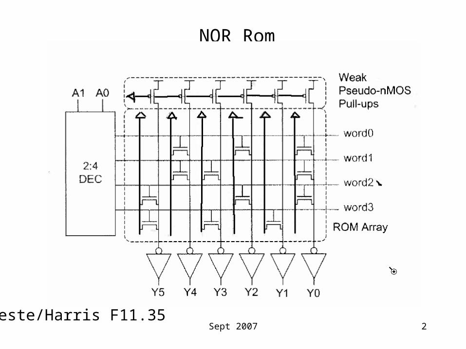
NOR Rom
Weste/Harris F11.35
Sept 2007 3
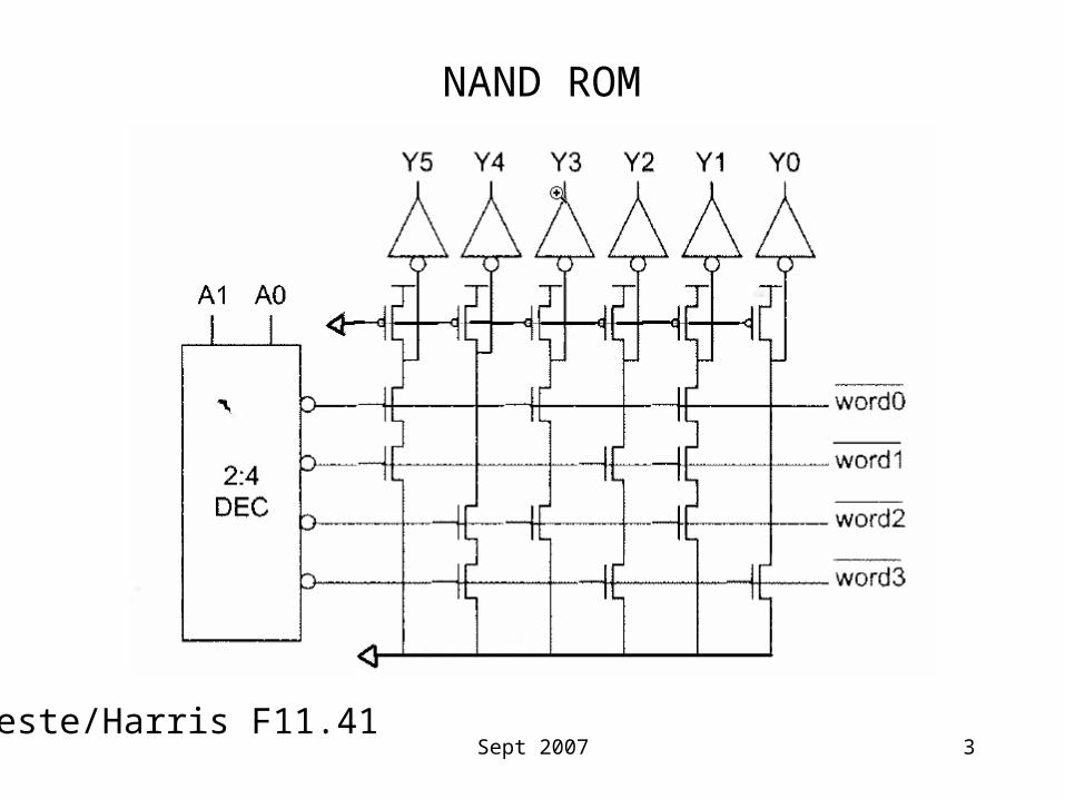
NAND ROM
Weste/Harris F11.41
Sept 2007 4
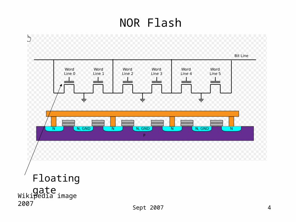
NOR Flash
Wikipedia image 2007
Floating gate
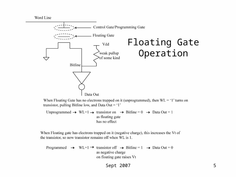
Sept 2007 5
Floating Gate Operation
Sept 2007 6
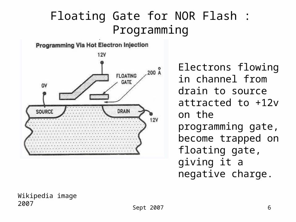
Floating Gate for NOR Flash : Programming
Electrons flowing in channel from drain to source attracted to +12v on the programming gate, become trapped on floating gate, giving it a negative charge.
Wikipedia image 2007
Sept 2007 7
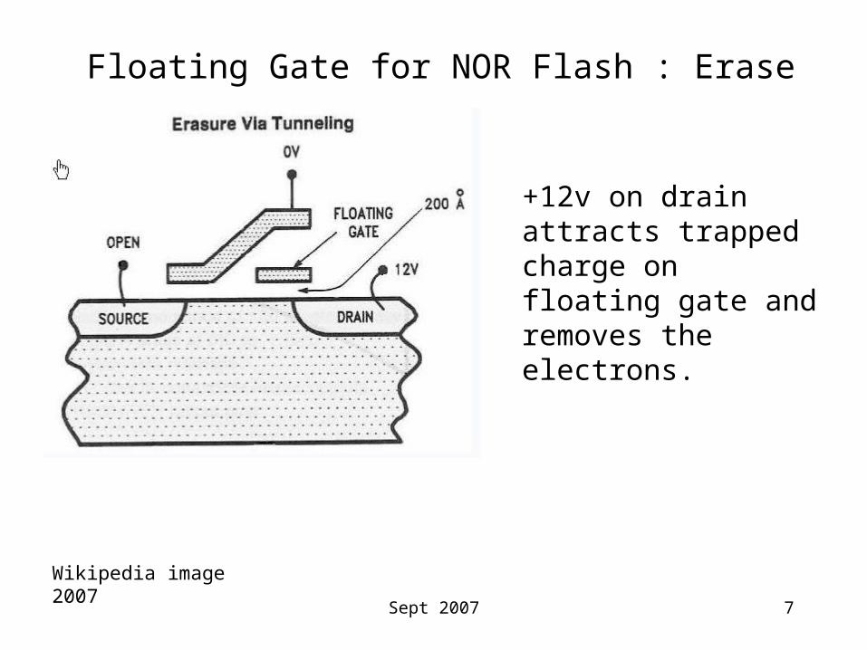
Floating Gate for NOR Flash : Erase
+12v on drain attracts trapped charge on floating gate and removes the electrons.
Wikipedia image 2007
Sept 2007 8
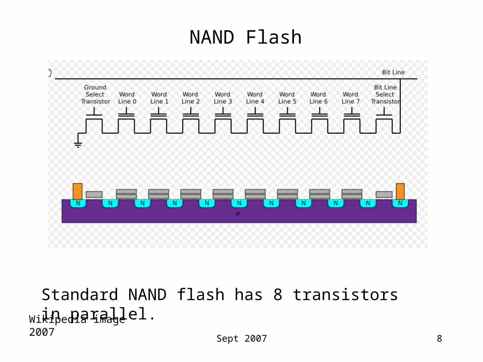
NAND Flash
Standard NAND flash has 8 transistors in parallel.
Wikipedia image 2007
Sept 2007 9
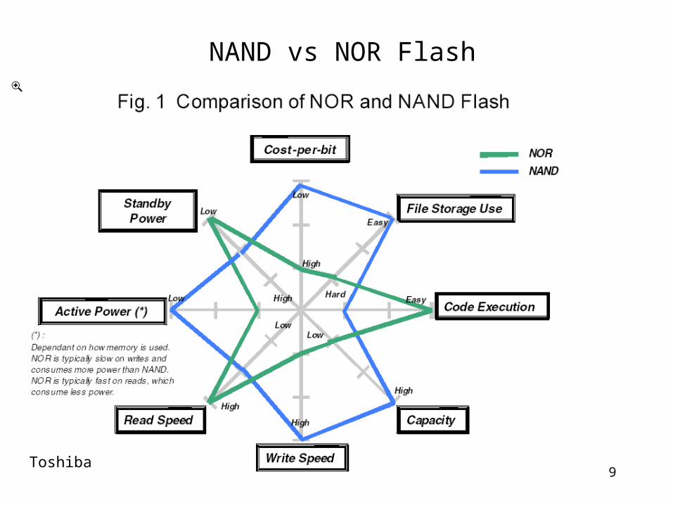
NAND vs NOR Flash
Toshiba
Sept 2007 10
NAND vs. NOR Flash
• NAND denser than NOR because of smaller cell size– preferred for data memory storage (flash drives)– NAND is about 2x denser than NOR because of layout efficiencies
due to series transistors (less metal contacts)
• NAND slower read time because of stacked cell arrangement– NOR preferred as program memory storage for microcontrollers
because of faster access time
• NAND is always block read/block write; NOR allows read of individual memory locations
• NAND programming/erase is faster than NOR programming/erase
Sept 2007 11
NAND/NOR Flash Limitations
• Both NAND/NOR memory has limited number of programming/erasure cycles
• About 100,000 cycles is a typical number, even though cells with higher cycle numbers can be designed– The Data memory EEPROM cells (100K minimum cycles, 1M
max) in the PIC microprocessors are designed to have about 10X the maximum number of programming/erase cycles as the program memory EEPROM cells (10K minimum cycles, 100K max)
Sept 2007 12
MRAM – Magnetoresitive Random Access Memory
• Semiconductor memory that uses magnetic storage elements• Advantages
– Non-volatile– Fast Read/Write (nanoseconds)– Random access– Unlimited read/write (does not degrade with usage like Flash)– Radiation hard (military applications)
• Disadvantages– Tough to scale down, IBM believes that scaling past 65 nanometer is
impractical– Stray magnetic fields can impact them, but packaging by Vendors gives
more than adequate protection from typical stray encountered fields
• Uses– Proponents believe will replace flash memory on microcontrollers since
these are not usually fab’ed with the most aggressive technologies, and some applications can benefit from the fast write times, and unlimited writes
– Could also replace SRAM/DRAM use in embedded systems.
Sept 2007 13
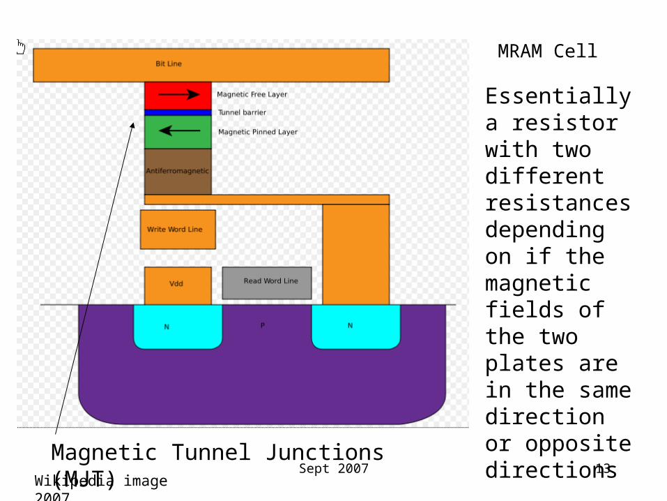
MRAM Cell
Essentially a resistor with two different resistances depending on if the magnetic fields of the two plates are in the same direction or opposite directions
Magnetic Tunnel Junctions (MJT)Wikipedia image 2007
Sept 2007 14
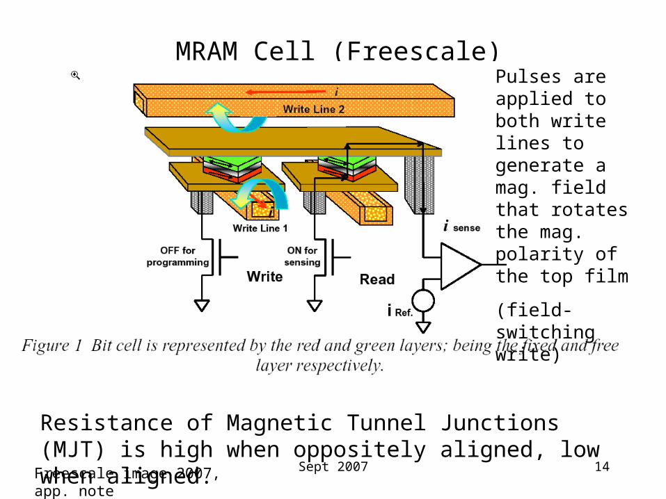
MRAM Cell (Freescale)
Resistance of Magnetic Tunnel Junctions (MJT) is high when oppositely aligned, low when aligned.
Pulses are applied to both write lines to generate a mag. field that rotates the mag. polarity of the top film
(field-switching write)
Freescale image 2007, app. note
Sept 2007 15
MRAM Operation• Two thin-film ferromagnetic films are used
– magnetic polarization of one film is fixed, the other is free to be changed to aligned to be the same or opposite of fixed field
• Electrons have two spins, ‘up’ and ‘down’, about 50% distributed and this changes as electrons move
• When electrons pass through ferromagnet, spins become spin-polarized– parallel with magnetic field (‘up’), majority carrier– anti-parallel with magnetic field (‘down’), minority carrier– ‘down’ spin electrons are scattered, ‘up’ spin electrons are not
• Electrons passing through two thin plates with same aligned fields means that only type of electron spin is scattered (looks like like low resistance, more electrons get through)
• Electrons passing through two thin plates with opposite-aligned fields means that both types of spin is scattered (looks like high resistance, less electrons get through).
Sept 2007 16
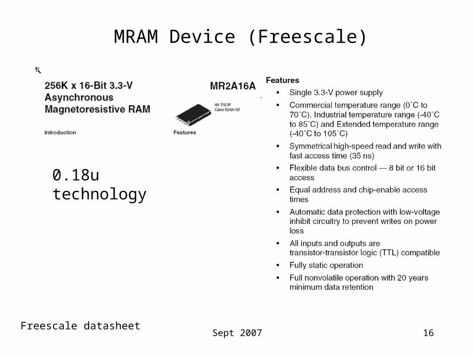
MRAM Device (Freescale)
0.18u technology
Freescale datasheet