semiconductor nonlinear optical waveguides lambkin, paul ... · download date: 17. feb. 2020....
TRANSCRIPT
University of Bath
PHD
Semiconductor nonlinear optical waveguides
Lambkin, Paul Martin
Award date:1990
Awarding institution:University of Bath
Link to publication
General rightsCopyright and moral rights for the publications made accessible in the public portal are retained by the authors and/or other copyright ownersand it is a condition of accessing publications that users recognise and abide by the legal requirements associated with these rights.
• Users may download and print one copy of any publication from the public portal for the purpose of private study or research. • You may not further distribute the material or use it for any profit-making activity or commercial gain • You may freely distribute the URL identifying the publication in the public portal ?
Take down policyIf you believe that this document breaches copyright please contact us providing details, and we will remove access to the work immediatelyand investigate your claim.
Download date: 18. Apr. 2020

Semiconductor Nonlinear Optical Waveguides
submitted by Paul Martin Lambkin for the degree of PhD
of the University of Bath July 1990
Attention is drawn to the fact that copyright of this thesis rests with its author. This copy of the thesis has been supplied on condition that anyone who consults it is understood to recognise that its copyright rests with its author and that no quotation from the thesis and no information derived from it may be published without the prior written consent of the author.
This thesis may be made available for consultation within the University Library and may be photocopied or lent to other libraries for the purposes of consultation.
p . —
- 1 -

UMI Number: U601755
All rights reserved
INFORMATION TO ALL USERS The quality of this reproduction is dependent upon the quality of the copy submitted.
In the unlikely event that the author did not send a complete manuscript and there are missing pages, these will be noted. Also, if material had to be removed,
a note will indicate the deletion.
Dissertation Publishing
UMI U601755Published by ProQuest LLC 2013. Copyright in the Dissertation held by the Author.
Microform Edition © ProQuest LLC.All rights reserved. This work is protected against
unauthorized copying under Title 17, United States Code.
ProQuest LLC 789 East Eisenhower Parkway
P.O. Box 1346 Ann Arbor, Ml 48106-1346

UNIVERSITY OF BATH LIBRARY
3 3 1 5 APR 1991
&

Summary
This thesis is an investigation of the properties of semiconductor, nonlinear, optical waveguides. The origin of nonlinearities in semiconductors is discussed and subsequent emphasis is given to the intensity dependent (Kerr-type) nonlinearity arising from band filling. Jacobi elliptic functions are introduced as the solution to the nonlinear wave equation governing electromagnetic propagation in media displaying such an intensity dependent nonlinearity. A detailed analysis of nonlinear guided waves in a planar structure is presented. This analysis is used to investigate two dimensional structures, for the first time, using a self consistent effective index approach. Finite nonlinear multilayer structures are examined with an emphasis on Bragg waveguiding configurations. These guides are shown to support nonlinear guided modes that have no linear counterpart. Finally, it is concluded that analytic solutions provide a straightforward and efficient method by which preliminary studies of nonlinear guided waves can be made.

To my mother and father
- 3 -

All persons in this book are real and none is fictitious even in part.
“ Mollycules is a very intricate theorem and can be worked out with algebra but you would want to take it by degrees with rulers and cosines and familiar other instruments and then at the wind-up not believe what you had proved at all. If that happened you would have to go back over it till you got to a place where you believe your own facts and figures as exactly delineated from Hall and Knight’s Algebra and then go on again from that particular place till you had the whole pancake properly believed and not have bits of it half-believed or a doubt in your head hurting you like when you lose a stud of your shirt in the middle of the bed.
- Very true, Mick decided to say.”
Flan O’Brien, The Dalkey Archive.

Acknowledgements
I would like to express my sincere thanks to Dr. K. A. Shore for his excellent supervision throughout the course of this work - diolch!
Thanks also to Drs. Mike Adams, Dave Mace and Mike Fisher of BTRL for their help and advice.
I am very grateful for the help and good humour of the Bath University electronics group past and present This includes John Kot, Martin McCall, Rob Norcross, Rob Noyes, Ian Middlemast, and Nigel Pennington. In particular, I thank Dr. J. Sarma for many helpful discussions that seldom failed to leave me with a sense of wonder, and thanks to Alice Bailey for helping with the layou, and speling. I feel that the computer officer, C. S. Chang, deserves special mention, not only for his inexaustable patience in the face of computing ignorance, but also for his creditable attempts to preserve South American rain forests.
I am indebted to Jane, my landlady, not only for feeding me on numerous occasions, but for letting me watch the World Cup on the colour telly. Finally, I should like to thank my family for all their support

Contents
Chapter One Nonlinear Semiconductor Optoelectronics
1.1 Introduction 1.11.2 Optical Nonlinearity 1.11.3 Nonlinear Optical Waveguides 1.21.4 Structure of the Thesis 1.21.5 References 1.4
Chapter Two Semiconductor Optical Nonlinearities
2.1 Introduction 2.12.2 The Electron Oscillator 2.12.3 Defocusing Nonlinearity in Semiconductors 2.22.4 Modelling the Nonlinearity 2.32.5 A Simple Band Filling Model 2.42.6 Nonlinear Optical Waveguides 2.72.7 Measurement of Refractive Index Nonlinearity 2.8
2.7.1 Techniques 2.82.7.2 Ellipsometry 2.92.7.3 Measurement Configuration 2.102.7.4 Results 2.122.7.5 Accuracy 2.152.7.6 Conclusions 2.17
2.8 References 2.19
Chapter Three Elliptic Jacobi Functions
3.1 Introduction 3.1
-6 -

3.2 Doubly Periodic Functions and Elliptic Functions 3.13.3 Theta Functions 3.23.4 The Elliptic Functions of Jacobi 3.3
3.4.1 Representation of Jacobi Elliptic Functionsas Fourier Series. 3.4
3.4.2 Jacobi Functions with Real orImaginary Arguments and Moduli 3.6
3.4.3 A Differential Equation InvolvingJacobi Functions 3.8
3.5 References 3.9
Chapter Four Planar Nonlinear Semiconductor Optical Waveguides
4.1 Introduction 4.14.2 Maxwell’s Equations 4.24.3 The Wave Equation 4.34.4 Nonlinear Waveguides 4.5
4.4.1 Analytical Solutions 4.7
4.5 TM Mode Solutions 4.94.6 Solution Technique 4.104.7 Guided Power 4.104.8 Verification of Programme 4.114.9 Verification of Analytic
Solution To Planar Guide 4.114.10 Planar Asymmetric Nonlinear
Waveguides 4.174.11 References 4.20
Chapter Five Nonlinear Rib Waveguides
5.1 Introduction 5.1

Chapter Six
Chapter Seven
5.2 The Effective Index (El) Method5.3 The Nonlinear Rib Waveguide Analysis5.4 Results5.5 Polarisation Effects5.6 Conclusions5.7 References
Multilayer Guiding Structures
6.1 Introduction6.2 Linear Multilayer Structures
and Transverse Resonance6.3 Nonlinear Multilayer Structures6.4 Periodic Structures
6.4.1 Bragg Reflection
6.5 Bragg Reflection Waveguides6.6 Nonlinear Bragg Reflectors
6.6.1 Method of Calculation
6.7 Results
6.7.1 Finite Linear BRW Properties6.7.2 Nonlinear Bragg Reflector
Waveguides
6.8 Conclusions6.9 References
Conclusions
7.1 Introduction7.2 Modal Interactions
5.15.35.7
5.155.155.16
6.1
6.26.46.7
6.7
6.8 6.10
6.11
6.12
6.12
6.14
6.206.22
7.17.1
-8 -

7.3 Material Effects 7.27.4 The Theoretical Treatment of
Semiconductor Nonlinear OpticalWaveguides 7.3
7.5 References 7.4
Appendix 1 TM Planar Analysis
Appendix 2 A Comparison Between Analytical and Numerical Results for a Nonlinear Rib Waveguide
Publications
-9 -

Chapter One
Nonlinear Semiconductor Optoelectronics
1.1 Introduction
In electronics a rich variety of phenomena, including rectification, modulation, harmonic generation, and heterodyning, arise from the nonlinear response of electronic processes. In the 1960’s the invention of the laser also enabled nonlinear responses to be obtained from optical processes. Nonlinear optics is concerned with the phenomena, some of which have analogues in electronics, that can subsequently arise. In principle, devices based on optical nonlinearity would achieve large bandwidths as a result of the high operating frequencies. This feature has motivated a great deal of interest in all-optical devices especially in the tele-communications industry where optics is already well established.
1J2 Optical Nonlinearity
Optical nonlinearity is manifested by changes in the properties of a medium subject to optical illumination. The fact that intense electric and magnetic fields are capable of inducing optical changes in a medium has been known for some time. Faraday discovered that the plane of polarisation of a light beam propagating in glass can be rotated by an applied magnetic field. This is known as the Faraday effect. Kerr, in a complementary experiment, showed that by applying a strong electric field in glass, light undergoes double refraction. This is known as the Kerr effect. From these results it is reasonable to suppose that if the electric and magnetic fields of a light beam are sufficiently strong, the beam itself will optically alter its ambient medium which in turn will affect propagation of the light beam. Such beams only became available with development of the laser. The high degree of coherence of the laser not only allowed the focusing of light on to small areas, but also enabled the weak contributions of nonlinear interactions from widely separated parts of a medium to be combined to produce an appreciable resultant.
Two general categories of optical nonlinearity can be distinguished. Intrinsic nonlinear phenomena can be described as violations of the principle of superposition arising from the nonlinear response of individual atoms, molecules,
- 1 . 1 -

or unit cells to incident waves. In general, this involves the conversion of input photons at a given frequency to output photons of different frequency, generated during interactions with polarisable material. This accounts for such phenomena as second harmonic generation and sum and difference frequency generation. Extrinsic nonlinearity is a change of properties which is directly related to changes in composition of the medium resulting from the absorption or emission of light. Intensity dependent refractive index is an important phenomenon that falls into this latter category. There is now a formidable body of literature devoted to these categories. An excellent overview is provided in the proceedings of the International School of Materials Science and Technology (Flytzanis and Oudar, 1985) (Boardman, 1989).
1.3 Nonlinear Optical Waveguides
In order to maintain high intensities and make efficient use of any nonlinearities present, guided wave geometries are used to confine the optical beams. For example the coherent coupler (Jensen, 1982) relies on the intensity dependent coupling between adjacent guides sharing a nonlinear coupling region. A comprehensive review of nonlinear interactions in guided wave geometries is given by Stegeman and Seaton (1985). Guided propagation is also essential to integrated optics which is based on the concept of combining different components in a single device. In the the now well established area of optical communications, sources and detectors are implemented using the semiconductor materials gallium arsenide (GaAs) and indium phosphide (InP). Integration would obviously be made easier if other devices were also fabricated in the same material system. Nonlinearity in semiconductors and the waveguide geometries in which they might be employed are thus of great importance. It is to these areas of interest that this work is directed.
1.4 Structure of the Thesis
In chapter two the origins of nonlinearities in semiconductors are discussed along with the restrictions subsequently implied for device design. That chapter concludes with a description of a refractive index measurement experiment performed to assess the feasibility of directly measuring nonlinear changes in refractive index . Elliptic functions, and particularly Jacobi elliptic functions are introduced in chapter three. They are shown to be the solution of a second order nonlinear differential equation. This equation is subsequently derived in chapter four as the governing equation for electromagnetic propagation in media
-1 .2 -

displaying an intensity dependent refractive index. A detailed analysis of nonlinear guided waves in a planar structure is then presented and a connection made with previous work in this field. In chapter five a two dimensional structure is analysed for the first time using a self consistent effective index approach. Finite nonlinear multilayer structures are treated in chapter six with an emphasis on Bragg waveguiding configurations. Finally, in chapter seven some conclusions are drawn concerning the role of analytic solutions in the analysis of nonlinear guided waves.
-1 .3-

1.5 References
A. D. Boardman and T. Twardowski, (editors), “ Nonlinear Optics: Materials and Devices,” Proceedings of the International School of Materials Science and Technology, Erice, Sicily, 1989, to be published.
C. Flytanis and J. L. Oudar, (editors), “ Nonlinear Optics: Materials and Devices,” Proceedings of the International School of Materials Science and Technology, Erice, Sicily, (1985).
S. M Jensen,“ The nonlinear coherent coupler,” IEEE J. Quantum. Electron., vol. QE-18, pp. 1580-1583, (1982).
G. I. Stegeman and C. T. Seaton,“ Nonlinear integrated optics,” J. Appl. Phys. vol. 58, pp. R57-R78, (1985).
-1 .4 -

Chapter Two
Semiconductor Optical Nonlinearities
2.1 Introduction
Optical nonlinearity in semiconductors has attracted considerable attention since the invention of lasers. The large nonlinear effects and compatibility with sources and detectors make integrated nonlinear optical devices a practical possibility. This has provided the motivation for what has become a large and sophisticated field of investigation. In this thesis emphasis is placed on the exploitation of nonlinear effects and so their origins are only given in outline. A more extensive explanation is given by Haug (1988) and Klingshim (1990). This chapter thus gives a brief description of the origins of nonlinearities in semiconductors and indicates the extent to which they have been measured and employed in all-optical devices. The chapter concludes with details of a series of experiments undertaken to measure the complex refractive index of semiconductors.
2.2 The Electron Oscillator
When an electric field E is applied to dielectric medium the bound charges are displaced against restoring forces. This creates internal dipole moments adding to the electric flux density. The sum of the internal dipole moments induced per unit volume is termed the polarisation P. The total flux density is thus:
D = eoE + P, (2.1)
where the polarisation is related to the applied field by:
P = XeoE. (2.2)
The total flux density then becomes:
D = eo(l+x)E. (2.3)
The dimensionless ratio x» known as the dielectric susceptibility, contains the essential optical properties of the material. It describes the various light / matterinteractions and so its complexity determines to what degree these phenomena are
-2 .1-

taken into account Alternatively the relative permittivity can be defined as:
e = ( l+ x ) . (2.4)
and the refractive index n as Ve.
An important optical characteristic is the frequency dependence, or dispersion, of the relative permittivity. Dispersive effects are greatest at certain frequencies resonant with atomic transitions. When the frequency © of the applied field is tuned close to that of a transition, the atoms acquire large dipole moments that oscillate at ©. The total field is then the sum of the incident wave and the field radiated by the dipoles. Since the radiated field is not in phase with the incident one, the effect is to change the phase velocity of the incident wave, or equivalently, to change the real part of the permittivity.
The calculation of the dipole moments of an atom can be treated within a sophisticated quantum mechanical formalism. More simply, an electron oscillating in a harmonic potential well can be used to empirically model the dipole moment. If the potential well is anharmonic the permittivity becomes field dependent and the medium exhibits intrinsic nonlinearity. Such a nonlinear optical response gives rise to numerous interesting phenomena (Stegeman, 1985) including second harmonic generation and Raman scattering.
23 Defocusing Nonlinearity in Semiconductors
Up to now it has been assumed that an optical system reacts instantaneously to the amplitudes of the incident electromagnetic fields. In extrinsic nonlinear processes the incident light generates species, such as excitons, electron-hole pairs, or phonons, that have finite lifetimes. The susceptibility will thus depend on their density at any given time. Since these excited particles usually undergo scattering during their lifetime, extrinsic processes are incoherent.
State or band filling is an example of such a process. The effect relies on Pauli’s exclusion principle which states that no two electrons in a crystal can be placed in the same quantum state. If an electron undergoes a given transition it blocks others from making the same transition. When a semiconductor is irradiated by an optical field close in frequency to that of the band gap, excited carriers fill the bands and reduce the number of initial and final states available for absorption. When the band is filled from the bottom up to the energy of excitation, the material becomes virtually transparent so that the absorption is fully saturated.
-2 .2 -

This negative change in the absorption affects the refractive index through the Kramers-Kronig relations:
A«(£) = - / 2 dE', (2.5)J tj (E’? - ( E ?
where E is the energy of the incident field and a is the absorption coefficient. As the bands fill, the interactions with the incident radiation become fewer and the effect is to reduce the refractive index as the local field intensity I increases. The negative change in refractive index means the nonlinearity is termed defocusing. The studies undertaken in this work are concerned with such defocusing nonlinearity. This is in contrast to much of the previous work on nonlinear guiding that has concentrated on the lithium niobate material system.
An early study of band gap resonant nonlinearity by Miller (1981) measureddtint = — , the nonlinear refraction coefficient, as -1.10r3cm2/W for InSb at 77K. dl
Measurements on GaAs / GaAlAs multiple quantum wells (MQW’s) (Miller, 1982) at room temperature showed the resonant effect to be very high; ri[ ~-2AQr5cm2IWy and lead to heightened interest in bulk semiconductors and MQW’s as promising passive optical materials.
2.4 Modelling the Nonlinearity
The optical properties of laser excited semiconductors are determined by the interactions between electron-hole pairs. Whilst the phenomenon can be accurately modelled by a quantum mechanical Greens function formalism, such a procedure is numerically intensive. Banyai and Koch (1986) developed a less sophisticated, partly phenomenological, description which was shown to be in good agreement with experimental data. In Figure 2.1(a-d) a comparison between theory and experiment, reproduced from Lee (1986), is given which clearly illustrates the relationship between intensity and absorption and the extent to which it has been successfully modeled. The top curve in Figure 2.1(a) is the low intensity absorption spectrum for bulk GaAs at room temperature whilst the subsequent curves show the spectra for increasing intensity. The resulting changes in refractive index, calculated using the Kramers-Kronig transformation, are given in Figure 2.1(b). Corresponding spectra calculated from the Banyai and Koch
-2 .3 -

plasma theory are given in Figure 2.1(e) and Figure 2.1(d).
1.501.50
Go As T=300K1201 2 0 -
0.90-^ 0.90-
0600.60
5 0.30- Q30-
10.0Go As T=300K0.03
0.02
- 0.020.03
-004
006-I-0.06 10.0150 -100138 144
Energy (eV)
Figure 2.1 Room temperature bulk GaAs optical nonlinearities: experiment and theory, (a) Experimental absorption spectra for different excitation powers P: (1) 0, (2) 0.2, (3) 0.5, (4) 1.3, (5) 3.2, (6) 8, (7) 20, (8) 50 mW on a 15 pm diameter spot, (b) Nonlinear refractive index changes corresponding to the measured absorption spectra. Curves a - g are obtained by the Kramers- Kronig transformation of the corresponding experimental data (2) - (8) in (a), (c) Calculated absorption spectra for different electron-hole pair densities N: (1) 1015, (2) 8 x 10¹⁶, (3) 2 x 10¹⁷, (4) 5 x 10¹⁷, (6) 1018, (7) 1.5 x 1018 cm-3. E° = 1.420 eV and ER = 4.2 meV . (d) Calculated nonlinear
refractive index changes. Curves a - f are obtained from curves (2) - (7) in (c), respectively.
2.5 A Simple Band Filling Model
A simpler model than that of the previous section can be derived using a rate
equation approach. Simplicity is achieved by relying on fitting free parameters. The density of electron-hole pairs N is governed by the following equation:
— + cc(°)’Ar) / (2.6) d t t E
Here x is the recombination time and E is the energy associated with the incident
-2.4-

light. Assuming steady state gives:
N _ a(w,N) j ^ 7)T E
If the relationship between carrier density and absorption is assumed to be linear then it follows that the change in absorption can be written as:
a = ao + cehN (2.8)
Similarly the change in refractive index An is given as:
n = n0 + q ehN. (2.9)
Using Eq. 2.8 in Eq. 2.7 gives:
a = — -----, (2.10)TGeh
where oto is the low intensity absorption coefficient. Defining a saturation intensity /, gives:
a = — where Is = - E . (2.11)i i
's
Miller (1982) showed that this expression accurately described the variation of a with intensity for GaAs / GaAlAs MQW’s. The variations were later successfully reproduced using the Banyai and Koch theory (1986). The change in refractive index can then be expressed as:
a „ = _ L ^ _ , (2.12)/,(! + 7 -)*S
where
/-> iAnm„ = - — — . (2.13)®eh
This rate equation approach to band filling is thus completely characterised by theparameters Anmsx and Is and has been used to duplicate measurements made ona GalnAs / InP MQW (Fisher 1989). A further simplification is to make a linear approximation to the variation of An with intensity. Thus a straight line,
-2 .5 -

coincident with the saturation curve at zero intensity and at the saturation intensity, is used to replace Eq. 2.12 and is written as:
A n(Is ) ^ ^ Y ~ = n,h- (2-14)
Finally the change in refractive index with intensity is given by:
n=no + ri[I (2.15)
where nt = . nmax and n0 is the low intensity, linear refractive index. This form of 2At
nonlinearity is said to be Kerr-like and has the considerable merit of permitting
analytical solutions to the wave equation to be obtained.
Comparison Between SaturationKerr—like Model of Nonlinearity
o.oo
- 0.01
• * Kerr—like Model —— Saturation Model
- 0.02 -
~oc - 0 .0 3 -
- 0 .0 4
10 1000 10000 100000100Intensiy ( W / c m 2)
Figure 2.2 The Kerr-like and saturation models of band-filling nonlinearity.
A comparison between the saturation and Kerr-like models for the change in refractive index is given in Figure 2.2 using a logarithmic scale for the intensity. The saturation curve is taken from (Fisher, 1990) where it was used to fit data
obtained from experiments on a GalnAs / InP MQW. The linear approximation is coincident at the saturation intensity beyond which the model becomes invalid.
-2.6-

Eq. 2.15 is thus a simple constitutive relation describing the optical response of a semiconductor when it is excited by radiation close to that of the band gap. It is clear from Figure 2.2 that this representation of the band filling nonlinearity has obvious limitations, but in the right circumstances still provides a valid characterisation of the nonlinearity and obviates the need for an intensive numerical approach. This will be demonstrated in the next chapter.
2.6 Nonlinear Optical Waveguides
The utilisation of nonlinear effects in semiconductor waveguide geometries is of great interest. To date the waveguide devices that have received the greatest attention are nonlinear directional couplers (Jensen 1982). The linear coupler simply consists of two adjacent guides. The power propagating in the composite structure oscillates between the individual guides over the coupling length. This is a result of beating between the modes of the coupler. If a nonlinearity is present then the coupling length will become intensity dependent allowing control over the proportion of power carried by each branch at a given length. However, in a waveguiding structure the absorption a must be less than about 100cm-1 and as can be seen from Figure 2.2(a) the absorption associated with the band edge itself is of the order of 104cm-1. Li Kam Wa (1985) pointed out that by operating off resonance an appreciable nonlinear response can be utilised without debilitating operating losses. Detuning by 30nm gave nj = -10-7 cm2/W and a =15 cm-1 enabling partial switching due to variation of intensity to be observed between the coupled waveguides. A similar approach has lead to the observation of bi-stability and nonlinear coupling between modes in passive GaAs / GaAlAs MQW waveguides (Li Kam Wa and Robson, 1987) (Li Kam Wa, 1988).
An alternative to detuning is to place the nonlinearity in a less sensitive part of the guide. Cada (1986) adopted this idea in a nonlinear vertical coupler. Here the nonlinearity was restricted to the medium between lossless guides. In this structure most of the energy is confined to the lossless regions and so advantage could be taken of on-resonant effects in the absorbing coupling medium. The principle was successfully demonstrated both by Cada (1988) and Berger(1988). However, different regions of a bulk semiconductor guide cannot be arbitrarily designated as nonlinear. Light is usually guided in the semiconductor medium of highest index which normally means the medium of lowest band gap. When the guide is excited by light of energy slightly below this gap (to obtain the nonlinear effect with small absorption) lower index regions will be non-absorptive and
-2 .7-

hence linear. To move to shorter wavelengths would be to risk crippling pandemic absorption.
Finally, it is noted that the band edge nonlinearity can be enhanced by prolonging the carrier lifetime. This can be achieved in n-i-p-i structures by spatially separating the electrons and holes (Kobayashi, 1988). Very large nonlinearities can be induced with nj = 0.05cm2!W giving lifetimes typically of the order of a ms (Kost, 1988).
2.7 Measurement of Refractive Index Nonlinearity
2.7.1 Techniques
Measurements of the nonlinear response of semiconductor materials have predominantly been undertaken using transmission experiments. This normally involves a pump and probe arrangement to obtain a series of transmission spectra in the region of the band edge for various pump intensities. The change in absorption can then be related to the change in refractive index by the Kramers Kronig relationship Eq. 2.5 . This was the approach adopted by Miller and Chemla (1982). Even more indirect routes are possible such as four wave mixing experiments (Miller, 1983) and the Mach Zehnder interferometer arrangement used by Li Kam Wa (1985).
Whilst the transmission experiments furnish relative changes in refractive index via absorption measurements, it would be useful to make direct measurements of the complex refractive index itself. A technique that might accomplish this and that has experienced a renaissance with the advent of the personal computer is ellipsometry. The next section describes a number of experiments using ellipsometry to measure the refractive index of some semiconductor substrates. These were performed at the British Telecom Research Laboratories in part fulfillment of the requirements of a SERC CASE award. These preliminary measurements were made to assess the technique as a suitable method for measuring nonlinear refractive indices.
-2 .8 -
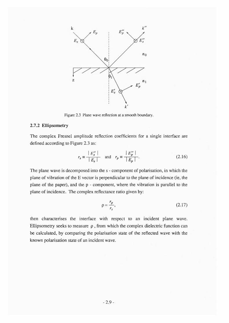
k'
Figure 2.3 Plane wave reflection at a smooth boundary.
2.7.2 Ellipsometry
The complex Fresnel amplitude reflection coefficients for a single interface are defined according to Figure 2.3 as:
I F" I I E ” Iand (2.16)
The plane wave is decomposed into the s - component of polarisation, in which the plane of vibration of the E vector is perpendicular to the plane of incidence (ie, the plane of the paper), and the p - component, where the vibration is parallel to the plane of incidence. The complex reflectance ratio given by:
P = — . (2.17)rs
then characterises the interface with respect to an incident plane wave.Ellipsometry seeks to measure p , from which the complex dielectric function canbe calculated, by comparing the polarisation state of the reflected wave with the
known polarisation state of an incident wave.
-2.9-

2.7.3 Measurement Configuration
S
L D
Figure 2.4 A rotating-analyser ellipsometer (RAE) consisting of a light source L, polariser P,
compensator C, system S, rotating analyser A, and detector D.
The system utilised in this work is the standard Polariser, Compensator, Sample, Analyser (PCSA) ellipsometer, which falls into the class of rotating analyser ellipsometers (RAE’s). The setup is shown in Figure 2.4 . Without the use of the compensator it is not possible to measure thin film or complex refractive indices by means of an RAE. The azimuth angles of the polariser, compensator fast axis, and analyser, are P, C, and A respectively and are measured clockwise from the plane of incidence. The phase retardation of the compensator is 8C. If the elements P and C are set and the analyser is rotated about the beam axis at a constant angular velocity, then the detected signal / has the form (Aspnes, 1974):
where Iav is the average flux incident at the detector. The experimentally determined quantities in an RAE system are the relative amplitudes:
f - l a v + /ccos(2A) + /ySin(2A), (2.18)
and p = y ~ .av
(2.19)
Here, 7av, Ic, and Is are determined from N sample values /V(v = 1, 2, 3,..., N) of the incident flux taken at equal intervals over one cycle of the sinusoidal component according to the following expressions:

X /». (2.20)N V = 1
/c = 4 i ^vcos(0,), (2.21)W V = 1
/ , 4 S ' « sW ' (2-22)N V = 1
where
0v=2lci i ^ i l . (2.23)N
The complex reflectance ratio is then given by (Azzam and Bashara, 1977):
,a 1 + a tan C + p ct a n ( / * - C )p = tamite1* = --------------------- — x- - ■—— , (2.24)r T l 1 - pctanC tan(P - C)
[ f } ± i ( l - a? - p 2)7 ]
where
P .- * 1*. (2.25)
The complex reflectance and the complex dielectric constant e = ei +*82 of a uniform, isotropic, reflecting surface in contact with an ambient medium whose dielectric constant is ea are related by (Aspnes, 1974):
— = [(1 - p) / (1 + p)]2 sin2<t>( tan24>j + sin2 <t>,-f (2.26)
where <j>,- is the angle of incidence. For real samples the above two-phase model (ambient and substrate) is not realistic, but it is useful to assume perfection and use the measured p to derive a “ pseudodielectric function” <e> using Eqs. 2.24,and 2.26 . The pseudodielectric function thus represents an average of the dielectric responses of the substrates and any overlayers (oxide layers etc.). In the experiments the compensator angle C was set to zero enabling the relative amplitude and phase shift of the p and s components of the incident flux to be determined independently by P and 8C respectively.
Aspnes (1974) has derived the conditions for which measurements are of maximum precision. The optimum value of 8C satisfies:
-2.11-

cos(A - 8C) = 0, (2.27)
and so results in the sin(2A) component in the detected flux vanishing. In this preliminary study transparent materials were first considered for which A = 0 , giving an optimum retardation 8C = 90° . The compensator was therefore adjusted to this value. Aspnes (1974) also showed that the optimum polariser angle Popt
will occur for
Popt = V (2.28)
When this condition is met the cos(2A) component in the detected flux will also vanish. The highest precision measurements are therefore made when circularly polarised light is incident on the detector which produces a constant output signal. It is possible to iterate towards the optimum conditions by resetting the polariser angle to a value based on a previously measured value of \j/. This scheme was adopted here in order to approach the situation where a = p = 0 .
2.7.4 Results
Using a semiconductor laser source operating at 1.582 [im and an automated data logging system, refractive index measurements were made on three different samples:
S i Si Doped substrate, roughened back surface,
52 InP Doped substrate, roughened back surface,
53 InP Undoped substrate, etched back surface,
with C = 0 , 5C = 90° and <j> = 57.4° . Results are summarised in Tables 2.1,2.2 and2.3 where n and k refer to the real and imaginary parts of the refractive index respectively. An example trace corresponding to experiment S.2.2 is given in Figure 2.5 . Superimposed on the data is the Fourier fit associated with Eqs. 2.20 - 2.23.
-2.12-

FLU
XEXPT S 2 . 2
77r-
46 —
1 5 -
160 210 240 270 300 330 36030 60 90 120 150
ANALYSER ANGLE A
Figure 2.5 Detected signal for experiment S.2 .2 .
-2.13-

Sample 5 1 Silicon
Experiment P° n k K Pt
S l.l 24.17 3.515 -0.072 23.90
S1.2 23.90 3.516 -0.070 23.91
S1.3 23.91 3.514 -0.068 23.89
TABLE 2.1
Sample S2 Indium Phosphide (doped)
Experiment P° n k Kpi
S2.1 21.26 3.173 -0.044 21.71
S2.2 21.71 3.171 -0.040 21.69
TABLE 2.2
Sample S3 Indium Phosphide (undoped)
Experiment P° n k K Pt
S3.1 21.71 3.229 -0.101 22.21
S3.2 21.12 3.224 -0.098 22.09
S3.3 22.09 3.225 -0.100 22.02
TABLE 23
-2.14-

The ellipsometric values can be compared to those taken from Willardson and Beer (1967).
Silicon
Wavelength \un n k
1.532 3.4784 -
1.6 3.4710 -
Indium Phosphide
Wavelength \m n k
1.500 3.172 -
1.549 3.167 -
1.600 3.161 -
1.653 3.156 -
2.7.5 Accuracy
The degree to which the pseudodielectric function <e> represents e will obviously depend on the extent to which the ideal two-phase model accurately describes the sample configuration. Semiconductor substrates exposed to atmosphere will form oxide overlayers and hence alter the dielectric function. For example, the rate of film growth during the atmospheric oxidation of Si after a HF rinse has been measured (Azzam and Bashara, 1977) as 6.86A/ decade of time in seconds. A more complicated three-phase model (substrate - overlayer - ambient) can be used in this situation corresponding to Figure 2.6, but requires additional measurements to determine the extra parameters. At around 1.5\im the overlayers are nominally transparent oxides. This means that only the thickness and ordinary refractive index of the overlayer need be determined. If the substrate is also transparent then and A become independent with y being only a function of £ i . Thus £i can be obtained directly with no interference from the overlayer. Even with these simplifications more effort is required to obtain e2 .
-2.15-

The most direct approach is to measure the film thickness d independently. Alternatively, measurements can be made at different angles of incidence. If, as in Figure 2.6, an 20A silicon oxide layer is assumed to be present, then the complex refractive index can be calculated a s :
n = 3.470, k =-0.046.
This does not compare favourably with the result from experiment S1.3 which gave:
n = 3.514, k =-0.068.
Air
SiO 2 n = 1.53
Si n =3.471 X= 1.5821im
d = 20A
<|> = 57.4°
Figure 2.6 A three-phase system.
Some indication of the sensitivity to the errors in the azimuth angles can be given by recalculating the dielectric function assuming a 1° error in retardation 5C and a 0.3" error in the fast axis angle C. This gives the following result:
n = 3.461, k = —0.093.
Whilst azimuth errors cannot wholly account for the inaccuracies of S1.3, they could make a significant contribution. The lack of symmetry in the flux trace will also lead to inaccuracies and is indicative of poor alignment or poor quality polarisers.
It has thus been demonstrated that the absolute measurement of the refractive index of a semiconductor at optical wavelengths is not straightforward. As it stands, the experiment requires considerable improvement to obtain accurate results. In an effort to establish whether relative changes could be reliably detected, a number of measurements were repeated with and without re-mounting the sample. Example results are given below in Tables 2.4 and 2.5:
-2.16-

Sample Sj Indium Phosphide (doped)
Experiment Comment P° n k
S2.2 First measurement 21.71 3.171 -0.040
S2.2.1 Repeat, sample not moved 21.71 3.170 -0.038
S2.2.2 Repeat, sample remounted 21.71 3.171 -0.039
TABLE 2.4
Sample S3 Indium Phosphide (undoped)
Experiment Comment P° n k
S3.3 First measurement 22.09 3.225 -0.100
S3.3.1 Repeat, sample remounted 22.09 3.216 -0.080
TABLE 2.5
These show that results are reproducible to within ~ 0.02 when a sample has been moved, with an order of magnitude improvement if the sample is undisturbed. The difference in result for the doped and undoped InP samples is most likely a function of their back surfaces. The doping levels involved would not produce a change in dielectric function detectable by this experiment
2.7.6 Conclusions
It has been established that accurate refractive index measurements were unobtainable with the experimental arrangement used. However, results were reproducible on a run-to-run basis making the detection of relative changes a possibility. Whether band filling induced index changes are resolvable by the present system can be determined by considering transmission measurements made on a GalnAs / InP MQW (Fisher, 1990). Here the maximum change in absorption was ~ 4000cm~l which corresponds, via the Kramers-Kronig relations, to a change in the real part of the refractive index of ~ 0.04. The change in the imaginary part can then be approximated by using:
-2.17-

f = X fc (Z 2 9 )
which gives ( Ak )mUi ~ 0.05 . This is indeed resolvable provided the sample is not disturbed between measurements. Despite ellipsometry being, in general, a powerful technique, transmission experiments would seem to provide a quicker and simpler method for measuring nonlinear intensity dependent refractive indices.
-2.18-
2.8 References
D. E. Aspnes, “ Optimizing precision of rotating-analyzer ellipsometers,” J. Opt. Soc. Am., vol. 64, pp. 639-646, (1974).
L. Banyai and S. W. Koch, “ A simple theory for the effects of plasma screening on the optical spectra of highly excited semiconductors,’ ’ Z. Phys. B, vol. 63, pp. 283-291, (1986).
R. M. A. Azzam and N. M. Bashara, ‘ ‘Ellipsometry and polarized light,” North- Holland publishing company, pp. 257-268, (1977).
P. R. Berger, Yi Chen, P. Bhattacharya and J. Pamulapati, “Demonstration of all optical modulation in a vertical guided-wave nonlinear coupler, ” Appl. Phys. Lett, vol. 52, pp. 1125-1127, (1988).
M. Cada, R. C. Gauthier, B. E. Paton, J. Chrowstowski, “ Nonlinear guided waves coupled nonlinearly in a planar GaAs/GaALAs multiple quantum well structure,” Appl. Phys. Lett, vol. 49, pp. 755-757, (1986).
M. Cada, B. P. Keyworth, J. M. Glinski, A. J. Springthorpe, and P. Mandeville, “Experiment with multiple-quantum-well waveguide switching element” J. Opt Soc. Am. B, vol. 5, pp. 462-466, (1988).
M. A. Fisher, “ Measurements of the nonlinear refractive index of a GaAlAs/InP multiple quantum well,” J. Appl. Phys. vol. 67, pp. 543-545, (1990).
H. Haug, “ Optical nonlinearities and instabilities in semiconductors” Academic Press, (1988).
C. Klingshim, “ Non-linear optical properties of semiconductors,” Semicond. Sci. Technol., vol. 5, pp. 457-469, (1990).
A. Kost E. Garmire, A. Danner and P. D. Dapkus, “ Large optical nonlinearities in a GaAs/AlGaAs hetero n-i-p-i structure, ” Appl. Phys. Lett., vol. 52, pp. 637-639, (1988).
-2.19-

H. Kobayashi, Y. Yamanchi and H. Ando, “ Nonlinear optical absorption in an n-InGaAsP/p-InP heterodoping superlattice, ” Appl. Phy. Lett., vol. 52, pp. 359-361, (1988).
Y. H. Lee, A. Chavez-Pirson, S. W. Koch, H. M. Gibbs, S. H. Park, J. Morhange, A. Jeffery, N. Peyghambarian, L. Banyai, A. C. Gossard, and W. Wiegmann, “ Room-temperature optical nonlinearities in GaAs,” Phys. Rev. Lett., vol. 57, pp. 2446-2449, (1986).
P. Li Kam Wa, J. E. Sitch, N. J. Mason, J. S. Roberts, P. N. Robson, “ All optical multiple quantum well waveguide switch,” Electron. Lett., vol. 21, pp. 26-27, (1985).
P. Li Kam Wa and P. N. Robson, “ Optical nonlinearities in a passive GaAs/GaAlAs multiple quantum well strain-induced waveguide,” IEEE J. Quantum Electron., vol. QE-23, (1987).
P. Li Kam Wa, P. N. Roberts, J. S. Roberts, M. A. Pate, and J. P. R. David, “ All optical switching between modes of a GaAs/GaAlAs multiple quantum well waveguide,” Appl. Phys. Lett., vol. 52, pp. 2013-2014, (1988).
D. A. B. Miller, C. T. Seaton, M. E. Price, and SJD. Smith, “ Band-gap resonant nonlinear refraction in ni-V semiconductors,” Phys. Rev. Lett, vol. 47, pp. 197-200, (1981).
D. A. B. Miller, D. S. Chemla, D. J. Eilenberger, and P. W. Smith, A. C. Gossard, and W. T. Tsang, “ Large room-temperature optical nonlinearity in GaAs/ Gaj.jAljAs multiple quantum well structures,” Appl. Phys. Lett., vol. 41, pp. 676-681, (1982).
D. A. B. Miller, D. S. Chemla, D. J. Eilenberger, P. W. Smith, A. C. Gossard and W. Wiegmann, “ Degenerate four-wave mixing in GaAs / GaAlAs multiple quantum well structures,” Appl. Phys. Lett., vol. 42, pp. 925-927, (1983).
G. I. Stegeman, C. T. Seaton, W. Hetherington, A. D. Boardman, and P. Egan, “ Nonlinear guided waves,” Proceedings of the international school of material science and technology, Erice, Sicily, July 1-14,1985, pp. 31-64.
-2.20-

R. K. Willardson, A. C. Beer, (editors), “ Semiconductors and Semimetals, volume 3, optical properties o f III-V c o m p o u n d sAcademic press, (1967).
- 2.21 -

Chapter Three
Elliptic Jacobi Functions
3.1 Introduction
One cannot proceed very far in the theory of nonlinear differential equations before encountering solutions expressed in terms of elliptic integrals or elliptic functions. In chapter four a nonlinear differential equation will be derived that governs electromagnetic propagation in a medium characterised by a Kerr-like nonlinearity. Jacobi functions are solutions to this nonlinear differential equation. They are the natural generalisations of the inverse circular and direct circular functions and are so called because they arose as a special example in the rectification of the arc of an ellipse. Since elliptic functions, and more particularly Jacobi functions, are relatively unfamiliar it is considered worthwhile to outline some of their properties here. The elliptic functions of Jacobi are derived in terms of theta functions which provide a method for their numerical evaluation. An alternative scheme of evaluation suitable for a purely real analysis is also outlined. Finally, the nonlinear differential equation whose solution is in terms of Jacobi functions is derived.
3.2 Doubly Periodic Functions and Elliptic Functions
Suppose that the function / (z ) , where z is in general complex, has two distinct periods 2<0i and 2<D2 s o that:
/ ( z + 2©1) = / ( z ) (3.1)
/ ( z + 2© 2) = / ( z ) (3.2)
COiFurther, let the periods have a complex ratio — so that there exists a network of
period parallelograms, or meshes, as shown in Figure 3.1. The periodparallelograms are called fundamental if they are the smallest such meshes for thefunction / (z ) . The values of / (z) in any parallelogram P are repeated in each of the other parallelograms as indicated by Eqs. 3.1 and 3.2 . Doubly periodic functions are a natural extension of the simply periodic trigonometric functions of
-3 .1 -

elementary mathematics. If a doubly periodic analytic function / (z) has, in the finite plane, no singular points other than poles, then / (z) is called an elliptic function.
Im
(2a>i + 2(02)
Re
Figure 3.1 The Period Parallelogram
33 Theta Functions
Theta functions were first developed systematically by C. G. J. Jacobi in his treatise Fundamenta nova theori fimctionum ellipticarum 1829. Four principaltheta functions have been recognised and are defined by means of the following(Rainville, 1960):
i 2ei(z.<7) = 2 E ( - W sin(2n + l ) z , (3.3)
11=0
1 2^ 2^ q ) = 2 ^ cos(2n + l)z , (3.4)
n=0
03(m ) = 1 + 2 E ?"2 cos(2nz), (3.5)»=i
64 = 1 + 2 2 (-1)"? “2 cos(2nz). (3.6)n=0
The only requirement on these functions is that I q I < 1 . It can be represented conventionally in the form:
-3 .2-

q = expOux), (3.7)
where x is a complex number of the form x = r + s i , in which s > 0 .
It can be shown that 03(z) and 04(z) have the common period k and that 0i and 02 have the common period 2tc , which reflects the periodicity of the sine and cosine functions. Another period might be expected in relation to the exponential q =exp(7u'x) since:
exp(K + 2tu) = expO*). (3.8)
It turns out that the theta functions are not doubly periodic, however, it is possible to use the theta functions to construct functions which are doubly periodic. Such functions are the elliptic Jacobi functions.
3.4 The Elliptic Functions of Jacobi
Dropping the q dependence of the theta functions and introducing a new
independent variable u , known as the argument, by z = —£■— three Jacobi03(0)
elliptic functions may be defined by:
*e2(0) 04(0 f (**))’, „ e3(0) e,(0j2(«))
sn (u) = — — ■ ■ ■ , (3.9)
, , e4(0) e2(0f(«))cn (u) = — —--------=------, (3.10)02(0) 0„(032(U))
04(0) 03(03J(«)) dn(u)= ■■ - (3.11)
where the parameter
02(0) 04(032O*)) ’
01(0)k = (3.12)
0?(0)
is known as the modulus and may sometimes be dropped from the functional notation. The periodicity properties of the functions sn(u), cn{u), and dn{u) may be written as follows:
-3 .3 -

sn (u + 4K) = sn (u + 2iK') = sn (w), (3.13)
where
cn (u + 4K) = cn(u + 2K + 2 iK') = cn (k),
dn (u + 4tf) = dn(u+ 4 iK') = (m),
(3.14)
(3.15)
(3.16)
and
je'=-yijwel(0). (3.17)
It can therefore be seen that 2K and K'i play roles similar to iz in the theory of the circular functions and ni in the theory of the hyperbolic functions. The Jacobi elliptic functions are consequently rich in special values and identity relationships (Byrd and Friedman, 1953).
3.4.1 Representation of Jacobi Elliptic Functions as Fourier Series.
Since 0?(O) = — , it follows that “ = -^ r > and so the following notationn 0f(O) 2K
shall be adopted:
giving
KV = ~2KU’
sn (u,k) =e3(Q)ei(v)e2(0)e4(v)’
(3.18)
(3.19)
cn (u,k) =e4(0)e2(v)02(O)04(v)’
(3.20)
dn (u,k) =04(O)03(v) 03(O)04(v)'
(3.21)
The expansions of the theta functions will result in the Jacobi functions being represented as the ratios of Fourier series and hence introduces the possibility of representing them as single Fourier series. This is indeed possible and the
-3 .4-

expansions are as follows (Davis, 1960):
sn(u,k) = 2 ^ r £ - 1 *** n-0 I —4
*+4_2n— sin(2n + l)v, (3.22)
— 4-cn(.u,k) = 2-p- £ ? cos(2w + l)v,
- = / > 1 — Qn =0(3.23)
<*.(«,*) = ^ + 2| - Z , 1+ j .^ - ■ cos(2wv). (3.24)
If v=x + iy and x = r + si, s > 0 , then the series will converge for all values of v
within the strip I y I < y iu , and represent the functions there. The only obstacle
to evaluating the Fourier series is computing q when k is given. A practical method makes use of the following:
_ i r 1- v f2L i + V F .
(3.25)
where
*'=Vi-*2,
is known as the complementary modulus. Eq. 3.25 can be written as:
e2(Q.«?4)63(0.4")
_ q + q9 + g25 + q49 + qtl + •l + 2 q A + 2ql6 + 2qi6 + 2q6*+ •••
which is now inverted and q obtained as the following series in / :
q = / + 2/5 + 1519 + 150/13 + 1,707/17 + 20,910/21 + 268,616/25 +
(3.26)
(3.27)
(3.28)
which converges rapidly for values of / less than . If / is close to ■—, then^ Z>
the convergence of Eq. 3.28 may be improved by using k instead of k' in Eq. 3.25 and computing q' instead of q . The value of q is then given by:
ln(q).ln(q') = icl . (3.29)
Values correct to 15 decimal places can thus be computed without prohibitive labour. This method was also used (Spencely and Spencely, 1947) to construct tables of elliptic functions to this accuracy. An example of the variation of the
-3 .5-
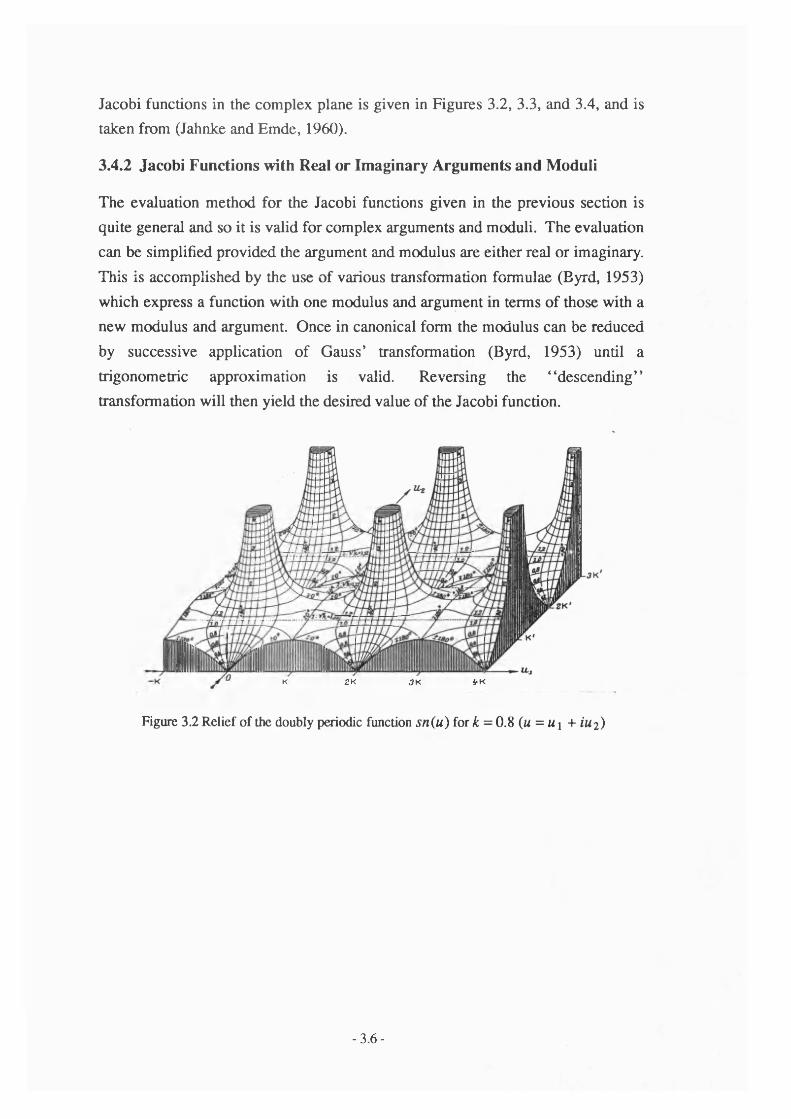
Jacobi functions in the complex plane is given in Figures 3.2, 3.3, and 3.4, and is taken from (Jahnke and Emde, 1960).
3.4.2 Jacobi Functions with Real or Imaginary Arguments and Moduli
The evaluation method for the Jacobi functions given in the previous section is quite general and so it is valid for complex arguments and moduli. The evaluation can be simplified provided the argument and modulus are either real or imaginary.
This is accomplished by the use of various transformation formulae (Byrd, 1953) which express a function with one modulus and argument in terms of those with a new modulus and argument. Once in canonical form the modulus can be reduced by successive application of Gauss’ transformation (Byrd, 1953) until a trigonometric approximation is valid. Reversing the “ descending” transformation will then yield the desired value of the Jacobi function.
K 2 K 3 K 4>K
Figure 3.2 Relief of the doubly periodic function sn(u) for k = Mi +iu2)0 . 8 (u =
- 3 . 6 -
86^845290865 501312962892040448

Figure 3.3 Relief of the doubly periodic function cn(u ) for k = 0.8 (w = u \ + iu.2 )
Figure 3.4 Relief of the doubly periodic function dn(u) for k = 0.8 (u = u \ + iu 2 )
- 3 . 7 -
238191

3.4.3 A Differential Equation Involving Jacobi Functions
The second derivative of the cn elliptic function can be written as:
d2cn(u) =(2/e2 - l ) Cn(U)-2 k 2Cn3(u). (3.30)du2
If a general solution is written as:
y = C c n (M x -x 0),k ) , (3.31)
where X and x0 are arbitrary constants, then it is possible to write:
(3.32)dxL CL
or
=Ay + By3, (3.33)dxL
where
= and C2= - ^ 2g ' 4 ) - (3.34)
The other Jacobi functions are also solutions to the second order nonlinear differential equation described by Eq. 3.33 .
The nonlinear differential equation Eq. 3.33 originates in a number of natural phenomena. For example, it describes the oscillations of a simple pendulum when the small angle approximation is no longer valid. In chapter four it will be shown that electromagnetic propagation in a medium characterised by a Kerr-like nonlinearity is also governed by Eq. 3.33 and hence has solutions in terms of elliptic Jacobi function.
-3 .8 -

3.5 References
Paul F. Byrd and Morris D. Friedman, “ Handbook o f Elliptic Integrals for Engineers and Physicists,” Springer - Verlag, (1954).
Harold T. Davis, “ Introduction to Nonlinear Differential and Integral Equations,” Dover publications, Inc., 2nd Ed., (1962).
E. Jahnke, F. Emde, and Losch, “ Tables o f higher functions,” McGraw-Hill book company Inc., New York, (1960).
Earl D. Rainville, “ Special Functions,” The Macmillan Company, 1st. Ed.,(1960).
G. W. and R. M. Spencely, “ Smithsonian Elliptic Functions Tables,” The Smithsonian Institute, (1947).
-3 .9 -

Chapter Four
Planar Nonlinear Semiconductor Optical Waveguides
4.1 Introduction
The general requirement for an electromagnetic waveguide is to confine the energy flow along the guiding structure and not perpendicular to it. This usually involves fields being confined to a high refractive index region by surrounding low index material. A simple optical waveguide that confines energy in one direction only is the planar or slab guide shown in Figure 4.1. It consists of a slab of high index material bounded by semi-infinite, low index regions. Not only is it a practical and frequently employed design, it can be solved analytically and so provides a unique physical insight into the nature of guided wave propagation. The linear slab guide, treated in many texts eg. (Yariv, 1985), represents a “ building block” in the understanding of more complicated structures and so the intention here is to study its nonlinear counter-part in some detail.
x1
dGadding n3
Core n2
0Substrate rii
n2 > n l > #3
Figure 4.1 A slab dielectric waveguide. Propagation in the z direction out of the paper.
-4 .1 -

4.2 Maxwell’s Equations
An electromagnetic field in space is described classically by two field vectors , Eand H called the electric vector and the magnetic vector respectively. The effectsof matter on the field are introduced via a second set of vectors D and B called the electric displacement and the magnetic induction . These vectors are related by Maxwell’s equations:
VxE + 4 r- = 0 , (4.1)at
VxH - = J , (4.2)at
V.D = p , (4.3)
V.B = 0 , (4.4)
where J is the explicit source term (amperes / square metre) and p is the electric charge density (coulombs / cubic metre). These equations are the basic laws of electricity and magnetism in differential form and fully describe the propagationof electromagnetic radiation in any medium. In studying optics it is usual toconsider radiation far away from any electromagnetic sources and hence J and p are zero.
To describe the effects that the material and fields have on each other Maxwell’s equations must be supplemented by the constitutive equations given by:
D = eE = CqE + P, (4.5)
B = PoH, (4.6)
where the parameter e is, in general, a tensor known as the dielectric tensor (or permittivity). P is the electric polarisation and eo and po are the permittivity and permeability of vacuum respectively. These equations represent a model of the material system interacting with electromagnetic radiation. The sophistication of the model is mirrored by the complexity of the dielectric tensor. For example, if the material is isotropic, the tensor reduces to a scalar. If the quantity e can be assumed to be independent of the field strengths - the material is linear. If this is not so then the material is classified as nonlinear. In chapter two the origin of the polarisation P was described and a constitutive relation derived for
-4 .2 -

semiconductors irradiated by light close in energy to that of the material’s band gap. It expressed the relative permittivity in terms of optical field intensity I ,
m = E*i = (n 0 +n,I)2 . (4.7)
Boundary conditions relating the field vectors E, H, D, and B either side of an interface between two media can be directly derived from Maxwell’s equations. For the situation when there is no free charge and no surface currents, the boundary conditions require that the components of D and B normal to the bounding surface, and the components of E and H parallel to the surface, are continuous across the boundary.
43 The Wave Equation
From Maxwell’s equations it is possible to write an equation governing the propagation of the electric field vector in a medium.
V2E(r, t) + V( - Moeotfr) | l - E ( r , ,) = 0. (4.8)e(r) 3r
where r is a space co-ordinate and t is time. If the variation of the dielectric constant is small in distances of the order of a wavelength little error is introduced
if Ve is neglected. The propagation equation becomes:
V2E(r, t) - noeoefr) |^ -E (r, t) = 0. (4.9)
Any function of the form / (r ± vr) will satisfy this equation where v is thevelocity of propagation given by:
V = - | r . (4.10)
and c is the velocity of light in vacuum:
c = - = ! = . (4.11)VeoMo
Here a harmonic solution is assumed such that:
E(r, t) = E(x, y) exp(i(cor - ^z)), (4.12)
-4 .3-

which describes propagation in the z direction. Using this expression in Eq. 4.8 and introducing the the time variation first gives:
V2E(r) + kl e(r)E(r) = 0, (4.13)
where
ko =©2Po£o» (4.14)
is the free space propagation constant Now introducing the z dependence for a rectangular co-ordinate system:
a2 + a2dx2 dy2
E(i,y) + [*§e(r)-tf]ECxI y) = 0. (4.15)
that — = 0 the TE mode contains only the Ey, Hx, and Hz components where the
A solution to this equation that satisfies the boundary conditions is called a mode of the waveguide. In linear analysis a general solution to a one dimensional guide can be represented as a linear sum of two polarisations, the transverse electric (TE) and the transverse magnetic (TM) modes with respect to the x-axis. Given
_a
electric field is restricted to the transverse plane. In this case, the electric field Ey and Ve will be orthogonal so E.Ve=0 and the reduction of Eqn. 4.8 to Eqn. 4.9 will be exact In contrast, the TM mode contains only the Hy, Ex, and£z components where the magnetic field is restricted to the transverse plane. Here
E.Ve*0 and Eqn 4.9 relies on the approximation -i-Ve = 0. Any linear
combination of the modes will be a solution of the waveguide. This property is known as orthogonality. Although for the nonlinear guide a linear sum of modes will not generally be a solution, the TE / TM analysis is still retained. A theory is first developed for the TE mode.
-4 .4-

4.4 Nonlinear Waveguides
xA
in Linear Cladding n3
II Nonlinear Core ~ n 2 + njl
ri[ < 0
I Linear Substrate nx
ti2>ri\> «3
Figure 4 2 A nonlinear dielectric slab waveguide.
Essentially, the use of nonlinear material in a guide structure allows the guide parameters to be altered or modulated by the incident light, thereby changing the field profiles in some useful manner, eg nonlinear directional couplers (Jensen, 1982). In the present work the origin of the defocusing nonlinearity is the absorption associated with the band edge of semiconductor material. This, as was indicated in chapter two, has an important implication in the guide design; namely, the nonlinearity will be present only in the high index core. With this consideration a suitable guide geometry is shown in Figure 4.2.
The TE mode is considered first for which the only electric field component present is Ey(x) . Since the slab guide is considered to be infinite in extent, there is
no field variation in the y direction and so = 0 . The equations governing thedy
electric field in the substrate and cladding are then written as:
-4 .5 -

d 2Ey ,Region I tt- + k\Ey = 0,
d x*(4.16)
d 2ERegion HI + %Ey = 0- (4.17)
Here the transverse propagation constants are introduced as:
k2 = i - k 2 and k2 = k l n 3 -k% , (4.18)
which represent conservation equations for the substrate and cladding. The solutions to Eqs. 4.16 and 4.17 will be of the form:
Region I Ey = E 0 exp(ik ix) , (4.19)
Region III Ey = E d expCik$(d- x ) ) . (4.20)
E 0 is the field amplitude at the interface between the nonlinear core and the linear cladding, whilst Ed is the field amplitude at the opposite interface. In line with the requirement to confine energy in the core region (Region II), the fields in Regions I and HI must decay exponentially. This will be achieved by satisfying the following k2 > klrii , given that rti > n 3 . Modes that fulfill this condition are referred to as confined or guided.
Attention is now turned to the core layer. From Eq 4.7 the dielectric constant is given as:
e(/) = ew = (n/ + n, / ) 2 (4.21)
Expanding the square and replacing /i/ by /12 gives:
Eni = n%i = n2 + 2n2*// + n fl2. (4.22)
The term n j l 2 may be neglected provided I « / 1 / c 2n2 . The intensity I is given by the Poynting vector which for the TE mode is:
/ = i — \ Ey \ 1. (4.23)2
Substituting and writing in terms of permittivity:
©Mo
hence
£«/ = 62 + n2 I Ey I 2, (4.24)
-4 .6 -

eni = e2 + CLni\Ey \ 2, (4.25)
where
a*/ =nznikz K n2n[ ^ njnj
co|io ” *o Moc \ioc(4.26)
Where the approximation — = n2 is valid for guides with a small dielctric step.KQWhen this expression is used in Eq.4.15 the following nonlinear wave equation is obtained:
d Ey
I h ?
and for purely real fields
+ [JfcjS(e2 + ow I Ey I = 0, (4.27)
d 2E„Y + kiEy + CL^klEj = 0,
d x
where
k\ =klz2~k].
(4.28)
(4.29)
The nonlinear differential equation described by Eq. 4.28 is recognised as being of the same form as the differential equation introduced in Section 3.4.3 and whose solutions were in terms of Jacobi elliptic functions, viz:
-4-2- + Ay+By3=0. d x 2
(4.30)
This was first pointed out by Akmediev (1982).
4.4.1 Analytical Solutions
Following Boardman and Egan (1986) a first integral of Eq. 4.28 is obtained as:f jr, V /dE,
d x\ /*2 +
klOyJE2y=C, (4.31)
where the constant of integration C can be written in terms of the boundary fields, Eq =Ey(x = 0) and Ed - Ey{x =d) , as:
-4 .7 -

a njElC = koEo ( £ 2 — £ 1 + —- — ),
. aniE2d— ^0 E d (£2 - £3 + — z — ) (4.32)
Figure 4.3 The hyperbolic relationship between the optical intensities at each of the core
interfaces. The portion of the curve falling inside the boxed region corresponds to guided modes.
Eq. 4.32 defines a hyperbolic relationship between the boundary field intensities as shown in Figure 4.3 . Real fields will be restricted to the positive quadrant and for
guided modes the following must also be true:
e2 - I ot^ I Eq > £ 1 and e2 - I I E j > £ 3 . (4.33)
For the structure considered here, where < 0 , only the portion of the curves falling within the boxed region indicated will give guided type solutions. A second integration of the nonlinear differential equation yields the Jacobi function solutions:
-4 .8-

E y - P cn(q(x + x0) ,m ) . (4.34)
Here cn is the Jacobi elliptic cosine function. The modulus is now designated m instead of the more usual k to avoid confusion with propagation constants. The parameter x0 is an integration constant. A comparison of Eqs. 4.28 and 4.30 gives the following:
m2= ^ n r - ’ (4-35)2?
and
(4.36)*00W
with
1q = (2kl<x«C + k b 'r ■ (4.37)
Applying continuity conditions to the Ey field and its derivative across theinterfaces, produces an eigenvalue equation:
, . , 2E0EAq2- k ik 3) „oxcn (qd, m) --------------------------------------- 75-------------- . (4.38)
k\El + k\El + q2[El +El) + ^ - l E l - E l f
In the limit = 0 , corresponding to a linear asymmetric guide, the above equation reduces to the form appropriate to a linear asymmetric slab waveguide (Yariv, 1985).
4.5 TM Mode Solutions
The TM modes involve E(EX, 0, Ez) and H(0, Hy, 0) . For such modes propagating in a medium characterised by an intrinsic nonlinearity the permittivity will be a tensor with a dependence on both electric field components (Boardman and Egan, 1984). As a consequence, an analytical solution is no longer available and the resulting wave equation must be solved numerically (Ogusu, 1989). In contrast, the refractive index associated with the incoherent band fillingnonlinearity remains simply dependent on the intensity and can be written as:
= e2 + a™ I Hy I 2, (4.39)
where
-4 .9 -
a TJ< = — . (4.40)©Co
An analytical solution, essentially similar to that of the TE mode, is still available and will be used in the next chapter to study two dimensional structures. The details of the TM nonlinearity, dispersion equation and the relationship between the fields at either boundary are given in Appendix 1 . The linear limit of the dispersion equation is also derived in the appendix and shown to be identical to that of the familiar linear TM eigenvalue equation.
4.6 Solution Technique
Returning to the TE analysis Eq. 4.32 describes the relationship between the field intensities at each interface. For a prescribed value of Eq the value Ed can be calculated with the sign of ±^Ed determining whether a solution will be even or odd. Values of E 0 and Ed can then be used in Eq. 4.38 and a numerical search made for values of kg that will satisfy it. Since the eigenvalue equation must be solved numerically the method is sometimes referred to as being semi-analytic. The quantity kg/kQ relates the phase velocity of the mode to the phase velocity of a plane wave in free space and is thus, notionally, a refractive index. It is therefore known as the effective index nejf. The eigenvalues kg can be used in the field equations Eq. 4.19 and Eq. 4.20 for the substrate and cladding and also in the following equation for the field in the nonlinear core:
qE0( qcn (qx) + k xsn(qx)dn(qx) )E ,--------------- — 2-------- . (4.41)
q2dn2(qx) + ko—j^ -sn 2(qx)
in which the dependence on the modulus has been suppressed.
Since no loss has been included in the analysis, the propagation constant kg will be real and so the arguments and the moduli of the elliptic functions will be either purely real or imaginary. In such circumstances, as indicated in chapter three, the functions can be evaluated using transformations.
4.7 Guided Power
The power carried by the guided wave will be given by:
-4.10-
Ptot ~£o
vMo,
VS- -v f 1 4 * -^0 _oo
(4.42)
Substituting for the form of the fields in the substrate and cladding yields:
P lot ~ kzv Mo,
OWiS 1 «»nlE d 12 *i
(4.43)
The integral of the field in the core can be cast in terms of elliptic integrals, but here a simple quadrature was used to evaluate it.
Finally, a normalised power flow PN can be introduced such that:
1Pn =
1 tot~Po'
p 0 =eo_
Mo *o(4.44)
Calculated results can therefore be quite general and applicable to a wide range of structures if distances occurring in the problem are normalised to the frequency using X = k0x . However, for the sake of definiteness, normalised results have not been quoted in the present work.
4.8 Verification of Programme
A computer code was written to perform the analysis outlined above to solve planar nonlinear waveguides. The programme was used to successfully reproduce results taken from (Boardman and Egan, 1986) and (Ogusu, 1986) where, in the latter, the special case of a symmetrical nonlinear waveguide was treated. Confident in the numerical integrity of the programme, the underlying theory could then be assessed.
4.9 Verification of Analytic Solution To Planar Guide
Here, in the absence of experimental data, results from the nonlinear planar waveguide programme are compared with those from a more elaborate treatment of the same problem (Gibbons and Sarid, 1987). In this way, it will be possible to highlight the present model’s strengths and weaknesses.
Resonant electronic nonlinearity in a semiconductor slab waveguide was first treated by Gibbons and Sarid (1987) and included carrier diffusion effects across the guide. The approach solved two second order differential equations, the wave equation and the carrier diffusion equation, by using a numerical integration in a
-4.11-

self-consistent way. The nonlinearity was modeled by the plasma theory of Banyai and Koch (1987) and takes into account the finite fraction of the optical power carried by a guided mode that must be absorbed to give rise to the nonlinearity. Consequently, a complex propagation constant k gives all the information necessary to propagate the mode. Since absorption, and hence £* , are carrier density dependent, it is necessary to recalculate k? self-consistently for each propagation step along the guide.
The analysis was applied by Gibbons and Sarid to three symmetric GaAs slab waveguides with AlGaAs cladding and operating at a wavelength detuned from the GaAs band edge. The AlGaAs cladding contributes nothing to the nonlinearity since its band edge is at a higher energy than that of the bulk GaAs. These guides are illustrated in Figure 4.4.
GaAs+3.524
0.2 p/w
GaAs+3.524
3.609
0.6 \xm
GaAs+
GaAs+
GaAs+3.597
3.609
A, = 893 run
l.Op/n 3.609
GaAs+
n(x) = Refractive Index Profile
Guide I Guide II Guide ID
Figure 4.4 The three guides analysed by Gibbons and Sarid (1987)
- 4 . 12 -

For each guide the effective index was calculated as a function of power per unit length relative to the linear value. The results for the change in effective index Aneff , with (L = lOp/n) and without (L = 0 ) carrier diffusion, are reproduced in Figures 4.5, 4.6, and 4.7 where L is the diffusion length. Gibbons and Sarid concluded that diffusion became significant in wide guides with relatively large core / cladding index steps. More significantly, for such structures the roll off in Art^was a result of the nonlinearity saturating. This was not true of the third guide where the core / cladding index step was small. Here the mode broadening means the increase in power is accommodated in the linear cladding and produces a roll off in Aneff .
Comparison with Sarid Analysis For Guide 1
o.ooo
- 0.001— Kerr—like♦ * Sorid L=0.0, 10.0 /xm
- 0.002
-0 .0 0 3
C< -0 .0 0 4
-0 .0 0 5
-0 .0 0 6
-0 .0 0 71.00.6 0.80.2 0.4
P o w e r ( m W / y u m )Figure 4.5 Comparison of results for Guide I between the Kerr-like model of semiconductor
nonlinearity and the plasma theory used in the Gibbons and Sarid (1987) analysis.
-4.13-

C o m p a r iso n with Sarid AnalysisFor Guide 2
o .o o o
- 0.002 -
- 0 .0 0 4 -
- 0 .0 0 6 -
c - 0 .0 0 8 -
- 0.010 - -Sarid L=0.0 Sarid L=10 .0 f im
- Kerr-like- 0.012 -
- 0 .0 1 4 -
- 0 .0 1 60.1 0 .2 0.3 0 .4 0.5 0 .6 0.7 0 .8 0.9 1.0
Power ( mW / yu,m )
Figure 4.6 Comparison of results for Guide II between the Kerr-like model of semiconductor
nonlinearity and the plasma theory used in the Sarid (1987) analysis.
-4.14-

C o m p a r is o n with Sarid AnalysisFor Guide 3
o .ooo
-0 .0 0 1 -I-Sarid L=0.0 /zm
Sarid L=10 .0 - Kerr-like
- 0.002 -
C -0 .0 0 3 -
-0 .0 0 4 -
-0 .0 0 5 -
-0 .0 0 60.2 0 .4 0.6 0.8 1.0 1.2 1.4 1.6 1.8 2.0
Power ( mW / )
Figure 4.7 Comparison of results for Guide III between the Kerr-like model of semiconductor nonlinearity and the plasma theory used in the Sarid (1987) analysis.
-4.15-

Results calculated from the analytic solution of the nonlinear wave equation have been superimposed on the Gibbons and Sarid curves in Figures 4.5 - 4.7 . A value tij =-1.2 lO-11 m2/W was used for the nonlinear coefficient to obtain the analytic
curves which provided a good match for guide in only. This value would seem reasonable and consistent with operating at a wavelength detuned from the exciton peak. For example, in an experimental demonstration of a GaAs / GaAlAs MQW waveguide switch (Li Kam Wa, 1985) the nonlinear coefficient was measured as nj — 10"11 m2/W . This was obtained for an operating wavelength of 850 run and with an exciton line at 820 run.
Figures 4.5 and 4.6 show that saturation and diffusion effects have become significant in guides I and II. Since neither effect is accounted for by the Kerr-like nonlinearity the match obtained for these guides is poor. However, it has been demonstrated that for a guide not limited by saturation or diffusion (ie. a guide with a small dielectric step) and using an experimentally consistent value of n j , a nonlinear modal analysis provides a realistic description of the nonlinear waveguiding phenomena in a planar structure. Furthermore, this has been achieved with a fraction of the computational effort required for the intensive numerical approach of Gibbons and Sarid. The modal properties of such guides are now investigated.
4.10 Planar Asymmetric Nonlinear Waveguides
Most work on semiconductor nonlinearities to date has concentrated on the GaAs / AlGaAs material system at wavelengths around 850 run . For telecommunications applications InP based materials are more attractive. They allow wavelengths close to 1.55 \m to be accessed which corresponds to the minimum absorption in fibres. In addition, the use of MQW structures allows independent tailoring of the band gap (and hence operating wavelength) and refractive index.
-4.16-

Nonlinear P lan ar Guide Field Prof i les
Cover nCore nSubstrate n.0.9 -
0.8 -
O 0 . 7 -0.421.282.283.605.939.23
" O 0 . 6 -
0.5 -
0 .4 -
0 .3 -
L±J 0.2 -
0.0210- 1
x Axis ( fj,m )Figure 4.8 Mode profiles of a semiconductor, defocusing, nonlinear, slab waveguide as the power
is increased.
Calculations have been performed for a waveguide fabricated in GalnAs / AlInAs MQW material, lattice matched to InP (Lambkin and Shore, 1988) corresponding to the structure of Figure 4.2 . The core was assumed to consist of 120 A GalnAs wells and 30 A AlInAs barriers, the cladding layer was taken to be formed with 60 A GalnAs wells and 30 A AlInAl wells. The structure is designed to have a
band edge nonlinearity at around 1.55 pm .
The dielectric constant of the core layer at this wavelength was estimated, using a weighted mean (Streifer, 1979) of the dielectric constants of the constituent ternary materials (Affomowitz, 1974), (Broberg and Lindgren) to be 11.76 . Similarly, the dielectric constant of the cladding was established as 11.42 . The cover layer is taken to be air of unity dielectric constant and thus the waveguide structure is strongly asymmetric. Using a representative value for the
-4.17-

semiconductor nonlinearity, n/ = - 1 10- 1 1 m2 / W , Figure 4.8 shows how the optical field profiles vary as the power is increased, whilst Figure 4.9 delineates the corresponding change in effective index. Since the the index difference between the core and substrate is reduced by the incident field, the effective index approaches the substrate index and the field begins to fill the semi-infinite region. Any additional power is thus expelled into a linear part of the guide and thus a limiting action is exhibited. This is illustrated in Figure 4.10 . In reality, if the guide index step is too great, the nonlinearity will saturate before the index difference has been washed out and the guide will not lim it By assuming a spot diameter of 1 \xm an estimate of the launched power to obtain the breakdown in guiding can be obtained as 10 mW .
Defocussing Guide3.394
3.392 -
3 .390 -
<D 3.388 - "O
3.386 -
3 .384 -
3 .382 -Lu
3.380 -Substrate index
3.3782 4 6 8
Power ( mW / )Figure 4.9 The power dispersion curve for a semiconductor, defocusing, nonlinear, slab waveguide.
-4.18-

Power in The Core2.5
E2.0
<DL_O 1.0
oc^ 0.5<D£o
CL0.0
862 4
Total P o w er ( mW / /xm )
Figure 4.10 A plot of the power confined to the core as a function of the total power, indicating
that the defocusing nonlinear waveguide behaves as an optical limiter.
-4.19-

4.11 References
M. A. Affomowitz, “ Refractive index of Ga\_xAlxA s ,” Solid-State Commun., vol. 15, pp. 59-63,(1974).
N. N. Akmediev, K. O. Boltar and V. M. Eleonski, “ Dielectric optical waveguide with nonlinear susceptibility. Asymmetric refractive-index profile,” Opt. Spectrosc. (USSR), vol. 53, pp. 403-405, (1982).
A. D. Boardman and P. Egan, “ Nonlinear surface and guided polaritons of a general layered dielectric structure,” Journal de Physique, Colloque C5, Supplement no. 4, Tome 45, pp. 59-63, (1974).
A. D. Boardman and P. Egan, “ Optically nonlinear waves in thin films,” IEEE J. Quantum. Electron, vol. QE-22, pp. 319-324, (1986).
B. Broberg and S. Lindgren,“ Refractive index of In \ _xGaxAsyP \_y layers and InP in the transparent wavelength region,” J. Appl. Phys., vol. 55, pp. 3376-3381,(1984).
W. M. Gibbons and D. Sarid, “ Effects of carrier diffusion on the nonlinear response of optical waveguides,” Opt Lett, vol. 12, pp. 564-566, (1987).
P. M. Lambkin and K. A. Shore, “ Asymmetric semiconductor waveguide with defocusing nonlinearity,” IEEE J. Quantum. Electron., vol. 24, pp. 2046-2051, (1988).
K. Ogusu, “ TE waves in a symmetric dielectric slab waveguide with a Kerr-like nonlinear permittivity,” Opt. and Quantum Electron., vol. 19, pp. 73 - 77, (1987).
K. Ogusu, “ TM waves guided by nonlinear planar waveguides,” IEEE. Trans. Microwave Theory Tech., vol. 37, pp. 941 - 946, (1989).
W. Streifer, D. R. Scrifies, and R. D. Burnham,“ Optical analysis of multiple- quantum-well lasers,” Appl. Opt., vol. 18, pp. 3547-3548, (1979).
-4.20-

Li Kam Wa, J. E. Sitch, N. J. Mason, J. S. Roberts, P. N. Robson, “ All optical multiple-quantum-well waveguide switch,” Electron. Lett., vol. 21, pp. 26 - 27,(1985).
A. Yariv, “ Optical Electronics,” Holt, Rinehart and Winston, (1985).
- 4.21 -

Chapter Five
Nonlinear Rib Waveguides
5.1 Introduction
A natural extension of the one dimensional planar waveguide is the two dimensional channel waveguide. Here lateral confinement of optical energy is obtained by introducing a y-direction perturbation in the refractive index or effective index. This can be achieved in semiconductor waveguides, for example, by compositional changes, as in a buried heterostructure, or by dielectric loading (eg. the addition of a rib). The solutions of the wave equation for a slab waveguide can be expressed in terms of TE and TM modes each of which are described by three field components. This simple description is possible because the fields are assumed to be independent of y. Two-dimensional guides not only require additional field components but also impose additional boundary conditions. However, the extra field components are not a major concern since they are normally small relative to the respective components corresponding to a slab guide. The imposition of further boundary conditions is more problematic and, in general, only satisfied by hybrid TE and TM modes. Analytic solutions to this problem are not possible and so require the use of either approximate or numerical techniques. A comparison of a number of the available methods has been made (Working group I, COST 216, 1989) which includes an evaluation of the popular effective index (El) method. This chapter briefly reviews the El method before applying it in a self-consistent way to a nonlinear waveguide. Results are presented and finally polarisation effects are considered in MQW guides.
52 The Effective Index (El) Method
A specific example of a channel waveguide is the rib guide illustrated in Figure5.1, where the co-ordinate axes and dimensions are defined. The El method establishes an “ effective refractive index” for the region inside the rib (region I) by solving the problem of a one dimensional slab waveguide formed if the rib were infinitely wide. A similar procedure for the region outside the rib (region II) solves for the slab waveguide obtained as if the rib width were zero. These
-5 .1-

effective indices are designated tii and nu , and define a further planar guide in
the orthogonal direction (see Figure 5.1).
Cladding n3
Core n2
Substrate n
nn ni nn
Figure 5.1 The rib-guide structure with the associated effective lateral guide.
The solution to this symmetric structure, with a core layer thickness w, can give a good approximation to the propagation constants of modes supported by the rib waveguide. If the transverse, x-direction, guides are solved for the TE mode, it is
usual to solve the lateral, y-direction, effective guide for the TM mode and vice- versa. An optical field distribution can be derived as the product of the field
profile given by the transverse calculation and the field profile given by the lateral calculation. The approximation inherent in this method is that by considering the waveguide initially as three distinct regions, field continuity has been ignored at the rib edges. The method is thus most accurate when the rib height is small, and the rib width is much greater than the height. In a nonlinear context these conditions are likely to be satisfied since the induced index perturbation should be
-5 .2-

of the same order as the maximum nonlinear change in refractive index. The propagation constants calculated by this method are greater than the true values (Working group I, COST 216,1989).
5 3 The Nonlinear Rib Waveguide Analysis
Nonlinear rib geometries have been used in a number of experiments to enhance nonlinear effects. Normandin and Houghton (1989) demonstrated an optical limiter for fibre optics using a channel waveguide. It consisted of a silicon thin film on a doped silicon substrate and relied on a defocusing, band filling nonlinearity at an operating wavelength of 1.06 p/n . Incident light from a fibre determined the refractive index profile in the coupling region of the guide and the resultant waveguiding conditions were computed in view of this imposed index distribution. The theoretical treatment did not consider nonlinear guided modes and only took planar geometry into account A modal analysis of a nonlinear rib guide has been given by Chrostowski and Chelkowski (1987), but this considered a self-focusing Kerr nonlinearity in the guide substrate.
The guide that will be treated here is the analogue of the guide illustrated in Figure5.1, with the core considered to be nonlinear . The dimensions are chosen for monomode operation in the linear regime, a property that will be preserved with increasing power by the defocusing nature of the refractive index changes. In essence, the analysis combines a series of x-direction nonlinear slab waveguides with a y-direction multi-layer linear guide to give a propagation constant nrib in the manner of an El approximation.
It has already been established that the shape of the electric field and the value of the modal index in a nonlinear slab waveguide depend on the value of the field E0 at the interface between the nonlinear core and substrate. In the rib guide E0 is now a function of the y-co-ordinate. Consider the rib guide to be divided into N+2 regions, as in Figure 5.2.
-5 .3-

X
A
0 M-l N B
Figure 5.2 Self-consistent multilayer (N-layer) model
Each region is then treated as an infinitely wide nonlinear planar guide that can be solved for an interface intensity value based on an E0(y) distribution. This will give for the i ’th region an effective index /i ,. The regions A and B can be treated as linear planar guides given that they are sufficiently laterally displaced from the rib for the optical field to be negligible. Due to symmetry, the effective indices for these regions will be equal and so are designated nA . The x-direction planar waveguide solutions can now be used to form an N layer, y-direction, linear waveguide. For a self consistent solution to the rib waveguide, the field associated with the multilayer solution nrib should correspond exactly with the E0(y) distribution used to generate the effective multilayer guide. If the correspondence is not within a tolerance, a correction must be made and the process repeated. An initial £oOO distribution is calculated assuming the guide to be entirely linear. In more detail the above technique involves the following steps:
1. Assign a value to Eq (0) that will remain unaltered for the calculation.
2. By assuming the rib to be linear, calculate a lateral field distribution <J>(y) .
3. For the i’th region calculate a weighting factor w, as follows:
W; = —— i = l,N , (5.1)$max
where 4>? is the average intensity in the i ’th region given by:
-5.4-

>i + AyJ <t>2Cy) y
.2 _ >*' ((5.2)Ay
and
<j>max = maximum (<J>?) i = 1, W . (5.3)
4. In each region solve the x-direction nonlinear planar guides using an interface intensity given by w,Eo (0) •
5. Recalculate <J>(y) and compare with the previous distribution.
6. Return to step 3 if the required tolerance is not met.
The linear multilayer problem is solved via a transverse resonant method, details of which are given in the next chapter. The El technique outlined here is capable of straightforward extension to other channel structures and can also take into account polarisation effects.
Some care must be taken when setting the number and width of the layers used in the y direction discretisation. To ensure that power calculations are realistic, the *‘window* * over which the integrations are made must be large enough for the field to become negligible at the window edges. It is also useful to note that wider strips can be used in the shoulder regions of the rib guide where the changes in the field intensities, and hence the effective index profile, will be slower. Conversely, a high packing density can be used under the rib itself where the fastest changes occur. Figure 5.3 shows how, for a fixed intensity Eq (0) , the calculated total power varies as a function of the number of layers used to discretise the guide over a given width. The method converges for increasing N, but more importantly, converges for the relatively small value of -30.
-5 .5 -

Pow
er
( (jW
)
Solution Convergence266
264
262
260
258
256
254
252
250
248
246
244
24210 15 20 25 30 35 40 45
Number of Layers ( N )
Figure 5.3 An example of the convergence of a solution of a nonlinear rib waveguide. N is the
number of layers used in the discretisation of the lateral effective guide.
-5 .6-

5.4 Results
Calculations have been performed (Lambkin and Shore, 1989) (Lambkin and Shore, 1988) for a guide fabricated with the same material parameters as the MQW, asymmetric, planar guide described in the previous chapter. The core is designed to exhibit a band edge nonlinearity at 1.55 \im and again a representative value of n/ = 10~n W/m is taken to model the nonlinearity. The shoulder thickness d is 1.01xm whilst the rib itself is 3 pm wide and 1.3 pm high; this means the guide is single moded. All calculations have been performed using N=45.
Figure 5.4 shows how the effective index of the whole guide nrib varies with total power. It also shows the variation with the power confined in the core below the rib, namely, the power in the channel. For completeness, results for a predominantly TM mode are also included. The behaviour can be explained in terms of the loss of lateral confinement as the optical field washes out the y-direction index perturbation. Lateral guiding is finally lost when nrib = nA . A limiting action can be observed by realising that the power in the channel is tending towards a constant, whilst the total power increases monotonically as the field spreads laterally. It is instructive to compare the effective index profiles for the low and high power solutions. In Figure 5.5 the depressed index profile, induced by the defocusing nonlinearity, is superimposed on the low power, linear profile. The fact that both coincide at the window edges indicates that the guide was considered over a sufficient width for the powers to be representative. The respective guide solutions have also been shown. The associated field intensity profiles are given in Figures 5.6, 5.7 . They are obtained by normalising the intensities to the value at the origin. If the guide were linear the distributions would therefore be identical for any power. In contrast, Figure 5.7 clearly shows that at the high power the lateral confinement is breaking down. The discontinuities in the contours represent errors induced by the El method failing to satisfy the boundary conditions at the rib edge.
-5 .7 -

Rib Guide Power Limiter3.401
TE Curves3.400
3.399 TM Curves
C 3.398
Q) 3.397 X>C 3.396
Total.Channel
<i> 3.395
Shoulder Eff Index (TE)3.394
3.393 -LU
3.392 -TotalChannel
Shoulder Eff Index QTM)3.391
3.39032 4 5
Power ( mW )
Figure 5.4 The power dispersion curves for the nonlinear semiconductor rib waveguide. Results are given for both TE and TM polarisations and the low power effective indices of the shoulder regions are also indicated. The curves labelled ‘Channel’ relate solutions to the power confined under the rib.
-5.8-

Eff
ecti
ve
Per
mit
tivi
ty
High Power and Lower PowerEffective Permittivity Profiles
.59
.58 -i t€> Low Power Profile
.57 -
Low Power Solution.56 -
.55 -
.54 -
.53 -
High Power Solution.52
.51 - High Power Profile
.508 - 6 - 4 - 2 0 2 4 6 8 10 12
y Axis ( )
Figure 5.5 A nonlinear, high power, lateral permittivity profile associated with nonlinear semiconductor rib waveguide. The linear, low power, profile is also shown, as are the solutions corresponding to the two cases.

I n t e n s i t y D i s t r i b u t i o n
rax15
m1cron5
CONTOUR KEY
0.30.50.70.9
- 0. 5
- 1 0 5 0 5 10
X a x i s m ic ro n s
Figure 5.6 Normalised intensity distribution for a linear, low power mode.
-5.10-

vi 13
o ~5
n —
3 in
- x
p
I n t e n s i t y D i s t r i b u t i o n
r
CONTOUR KEY
0.3
- 0. 5 0.7
- 1 0 5 0 5 10
X a x i s m ic ro n s
Figure 5.7 Normalised intensity distribution for a nonlinear, high powered mode.
-5.11-

It is immediately obvious from Figure 5.5 that the nonlinearity outside the rib mitigates against the suppression of a lateral index step. If the nonlinearity were confined to the rib only, then the limiting should occur at lower powers. This is confirmed in Figure 5.8 where calculations have been performed for such a
structure and compared with the previous one. The more efficient use of the defocusing nonlinearity means that the limiting occurs for powers reduced by ~
2/3. For approximately the same power represented in Figure 5.7, Figure 5.9 shows the permittivity profile for the modified structure. The lateral perturbation has almost vanished and as a result the lateral spreading of the intensity has greatly increased. This is illustrated in Figure 5.10.
Comparison of Limiter Structures3.401
3.400 Structure I
Structure3.399
<D 3.398 T ) Total Power
Power in Channel3.397 -
3.396 -
3.394 -
3.39332 4 5 6 7
Power ( mW )Figure 5.8 A comparison of power dispersion curves for Structure I - Nonlinearity present in rib and shoulder regions and Structure II - Nonlinearity under rib only.
-5.12-

Eff
ecti
ve
Per
mit
tivi
ty
Effective Permittivity Profiles For Second Structure
11.59
I 11.58 - Low Power Profile
11.57 -
Low Power Solution11.56 -
11.55 -
11.54 - High Power Profile
11.53 -
11.52 -
11.516 - 4 - 2 0 2 6 8 10 1
y Axis ( //.m )
Figure 5.9 A nonlinear, high power, lateral permittivity profile associated with Structure II - Nonlinearity under rib only. The linear, low power profile is also shown.
-5.13-

I n t e n s i t y D i s t r i b u t i o n
rax1s O
CONTOUR KETCron5
0.30.50.70.9
- 0.5
1055 0- 1 0
X a x is m ic ro n s
Figure 5.10 Normalised intensity distribution for a nonlinear, high powered mode. The
nonlinearity is restricted to the region under the rib.
-5.14-

5.5 Polarisation Effects
For the calculations presented here it has been assumed that the nonlinearity corresponding to TE and TM modes will be equal. This is not likely to be the case for multiple quantum well waveguides. Absorption should be significantly reduced for light polarised perpendicular to the layers. This has been experimentally demonstrated both in a single quantum well waveguide (Weiner, 1985) and in a GaAs / AlGaAs MQW nonlinear directional coupler (Jin, 1988). In the latter experiment the excitonic resonances for the light polarised parallel and perpendicular were separated by approximately 6 nm. Weiner (1985) suggested that an additional degree of freedom in guide design would be introduced by this “ strong linear and nonlinear dichroism” . However, by operating away from the excitonic resonance, as in the guides considered here, the dichromatic effect will be greatly reduced.
5.6 Conclusions
A straightforward method of calculating the mode shapes of channel waveguides with a nonlinear film has been presented. The method should provide a good approximation to the exact solution given that:
(i) The rib width is sufficiently large with respect to the core thickness.
(ii) The film to substrate index step is relatively small.
This is confirmed by a comparison, presented in Appendix 2, between results from the semi-analytical approach given here and results from a numerical investigation using the Beam Propagation Method (BPM).
-5.15-

5.7 References
J. Chrostowski and S. Chelkowski, “ Analysis of an optical rib waveguide with a nonlinear substrate,” Opt. Lett., vol. 12, pp. 528 - 530, (1987).
R. Jin, C. L. Chuang, H. M. Gibbs, and S. W. Koch, J. N. Polky, G. A. Pubanz, “ Picosecond all-optical switching in single-mode GaAs/AlGaAs strip-loaded nonlinear directional couplers,” Appl. Phys. Lett., vol. 53, pp. 1791 - 1793,(1988).
P. M Lambkin and K. A. Shore, “ Non-linear semiconductor ridge waveguides,” in TEE Colloquium on Nonlinear Optical Waveguides (Institution of Electrical Engineers, London, 1988), paper 12, (1988).
P. M. Lambkin and K. A. Shore, “ Analysis of an optical rib waveguide with a nonlinear substrate,” J. Opt Soc. Soc. Am. B, vol. 6, pp. 669 - 674, (1989).
R. Normandin and D. C. Houghton, “ Fully adjustable optical limiter for fiber optics using silicon films,” Appl. Phys. Lett, vol. 54, pp. 1836 - 1838, (1989).
J. S. Weiner, D. S. Chelma, and D. A. B. Miller, H. Haus, A. C. Gossard and W. Wiegmann, C. A. Burrus, “ Highly anisotropic optical properties of single quantum well waveguides,” Appl. Phys. Lett, vol. 47, pp. 664 - 667, (1985).
Working group I, COST 216, “ Comparison of different modelling techniques of longitudinally invariant integrated optical waveguides,” IEE. Proc., vol. 136, Pt. J, pp. 273-280, (1989).
-5.16-

Chapter Six
Multilayer Guiding Structures
6.1 Introduction
Multilayer configurations occur frequently in optical device design eg. superlattices and MQW’S. The analysis of stratified media can also be applied to effective multilayers generated by replacing a continuous effective profile by a large number of homogeneous layers. This technique has been applied to the problem of bending losses in curved waveguides (Ghatak and Thyagarajan, 1989), and was used earlier in chapter five to study the mode profiles of nonlinear ridge guides.
This chapter firstly considers linear multilayer structures with particular emphasis placed on periodic structures and the phenomenon of Bragg reflection. The ideas of transmission matrices and transverse resonance are introduced using an equivalent transmission line analysis of linear structures. Analogous nonlinear structures are then considered and an analysis of a finite, nonlinear, Bragg reflection waveguide is presented.
6.2 Linear Multilayer Structures and Transverse Resonance
The structure whose guided modes are being sought is shown in Figure 6.1. Only the TE modes will considered so the the electric and magnetic fields will be given by E = E(0, Ey, 0) and H = H(Hx, 0, Hx). Assuming harmonic solutions, the only non-zero electric field component is written as:
in each of the N + 2 layers where the transverse propagation constant is given by:
Ey(x, z, t) - Ey(x) exp ( i (©t - kjz) ) .
A mode will then be given by the solution of the scalar wave equation:
(6.1)
(6.2)
(6.3)
-6 .1-

Cl
= o
£n An
Figure 6.1 Multilayer Dielectric Guide
Similarly the equation governing the transverse magnetic field will be:
d 2Hz
~ d72+ k l lHzn= 0 , (6.4)
The transverse wave Eqs. 6.2 and 6.4 governing Ey and Hz are exactly analogous to those governing the voltage V and current I on a transmission line. As a result, the dielectric multilayer guide can be modelled by an equivalent transmission line network for which analysis techniques are well established. The method involves replacing each dielectric layer by a transmission line element as in Figure 6.2 .
In hn
In
- Q
6 Q -O
Figure 6.2 Transmission Line Element
-6.2-

The characteristic impedances are given for the TE mode as:
©Mo (6.5)
and by analogy
V(x)=Ey(x), /(*) = //,(*), Z(x) =__ V(x) _ gy(*)/(*) //zW
(6.6)
The solution method relies on the ability to relate the input and output impedances via the following relationship (Whinnery and Van Duzer, 1984):
V 2n
V _ ""
- / Zrt tan(^rfn)
InZ n - ^ r L ta n (k xndn)
I In
(6.7)
or more conveniently
V u V 2n
I In»pr„] (6.8)
where
COS0„ iZ„ sin0n
z-^-sin0* cos0n(6.9)
and
6 n = M n • (6.10)
The matrix Tn is known as the transmission or ABCD matrix for the circuit element. It simply relates the the input and output voltages and currents (Ey and H z) for the circuit element of the network. A transmission matrix for the whole network is formed by multiplying all the constituent matrices for each element The final equivalent circuit is now represented by Figure 6.3 where:
(6.11)
(6.12)
V u V tn
I n = [Tn1 I lN
and [T] = f l [ T H]n=1
-6 .3-

Ns x«=1
-o
zd
Figure 6.3 The Lumped Equivalent Transmission Line.
Suppose that the input impedance of the dielectric in region x > d on the surface x = 0 is ZM, and that for the region x <d it is Zd. The principle of transverse resonance then states that the condition,
Zu +Zd = 0 , (6.13)
is necessary for a guided mode to exist (Collin, 1960). Since Zu = Z4 and Zd is given by Eq. 6.11 the resonance will produce the following eigen value equation:
T + — — +ZA(T21 + ——) = 0 . (6.14)
As in the case of the single slab guide, a guided mode will be exponentially decaying in the substrates and so Z^and ZB will be purely imaginary. The solution
technique is based on the a-priori knowledge of the form of these fields. For a
given kt the method involves testing the continuity of one of the fields across a chosen interface given that all the fields have been matched at all the other boundaries. The transverse resonance technique was used to solve the multilayer guides arising from the analysis of nonlinear two dimensional structures treated in chapter five.
6.3 Nonlinear Multilayer Structures
The problem of a Kerr-type nonlinearity occurring arbitrarily in a multilayer system was first addressed by Trutschel et al (1988). They considered layers,
-6.4-

either linear or nonlinear, sandwiched between two linear bounding media. Their method of solution is, in essentials, identical to that outlined for the all-linear guide described above. It relies on the ability to construct a transmission matrix that relates the transverse components of a field at one interface of a layer to the components at the other. For a TE mode the components are Ey and Hz, or
equivalently Ey and Ey, where the derivative is with respect to x. The major difference from the linear analysis is that the matrix elements A, B, C, and D will
themselves be functions of the interface fields, and will be described by Jacobi elliptic functions. As expected the mode solutions in the nonlinear case will therefore be power dependent
E \ n(x) E 2n(X + d n)
E l n i x ) E2 n(x + d n )
E/i-l
d n - l HC------------------ 3*4
£n + 1
d n + 1
-3» X
Figure 6.4 The n’th Nonlinear Layer
Consider the n ’th layer in a stack shown in Figure 6.4 . It is assumed to be characterised by the following Kerr-type nonlinearity:
£„/(*) = £„ + 0 ^ I E I 2 , (6.15)
with a background linear dielectric constant of e„. The field inside the layer is assumed to vary as:
En(Xn) = Pn cn(qn(Xn - X 0n), mn) , (6.16)
where Xn =k0x . The relationships of Pnik^), <7,,(/:**),and m ^ k ^ ) to each other have already been established in the treatment of the nonlinear planar guide and
are given by Eqs. 4.32 - 4.34 . The fields inside the layer are then related to the input fields by:
-6 .5-

where
En(Xn) 4 . Bn EnO
1
Cn Dn En0(6.17)
cn(qnX„, m„), (6.18)
B" q,RnQCn)sn(qnXn, mn) dn(qnXn, mn) , (6.19)
c n = sn(4*Xn’ mn)dn(qHXn, mn) ,En\Xn)
(6.20)
A. = S2 "\ cn (qnXH, mn) ,Ri(XH)
and use has been made of the following abbreviations:
/?„(*„) = 1 - mn( 1 - --=-) sn2(qnXn, mn) ,
(6.21)
(6.22)
Sn(X„) = 1 -m„(l - - ^ r ) [1 + cnz(<7„X*f m j] , Pi
(6.23)
E2r.CST.) = 1 - m»(l + - £ - ) sn2(?„X„. m„). (6.24)
As in the linear multilayer guide, the solution technique requires an a-priori knowledge of the fields in the substrates. These are taken as exponential for a guided mode. For a given electric field value at a substrate boundary, say E (x = 0), then E(x = 0) is automatically determined by a ^ and the restriction of an exponential decay. The transmission matrix can then be used to move consecutively across the remainder of the guide to the opposite half-space boundary. Here the output field and derivative can be tested for consistency with the assumption of exponential decay in this region. Any linear layers within the stack will also be adequately treated by the transmission matrix since in the linear limit the moduli of the elliptic functions will become zero and the matrix will reduce to that given in section 6.2 .
-6.6-

6.4 Periodic Structures
A comprehensive theory of electromagnetic propagation in periodic stratified media was first presented by Yeh (1977). It has a strong formal similarity to the quantum theory of electrons in crystals and hence makes use of the concepts, familiar in the study of transmission lines, of Bloch modes and forbidden gaps (Brillouin, 1953). Here the subject will be introduced via a less rigorous ray optics approach using the idea of Bragg scattering and the Bragg condition.
6.4.1 Bragg Reflection
x
a
Unit Cell
v
______________________________________________Cl
e2
Figure 6.5 The Bragg Condition
Consider a plane wave incident upon a stack of periodic dielectric layers at an angle 6, as shown in Figure 6.5 . It is further assumed that the fractional difference between ei and 62 is small. Under these circumstances ray optics can be applied to determine the angle of incidence for a strong reflection. The restriction on the dielectric constants means transmission changes in propagation angle can be ignored, but at each boundary a fraction of the incident power will be reflected due to the discontinuity. For a strong reflection these contributions must add in phase so that:
t 2 y = 2ion. (6.25)
The solution for m = 1 is called the first order Bragg condition and is given by
9*- zA
y 2
2
- 6.7 -

k sin(0fl) = 27C/A, where 0B is the Bragg angle.
From this analysis two points can be made. Firstly, for the Bragg condition the amount of transmitted energy will be a decreasing function of the number of layers and for an infinite stack the reflection will be total. Secondly, the fields in the stratified medium will decay away from the* = 0 interface. In fact the fields in this region will be described by Floquet’s theorem giving an electric field of the form:
Ek (x, z) = Ek (x) exp( iKx ) exp( i l^ z ), (6.26)
where EK(x) is periodic with a period A , ie:
EK(x + A)=EK(x). (6.27)
The constant K is known as the Bloch wave number. For the decaying fields associated with Bragg reflection K must therefore be complex. Values of it* and co for which this is true are said to lie in the “ forbidden ” bands of the periodic medium. In general, the unit cell will consist of layers of unequal thickness and the 2rc phase change will accumulate over each cell, as opposed to each individual layer, so the real part of the Bloch wave number can be written down immediately as:
7XrK =m2% or K, = - . (6.28)A
where
K = Kr + iKi. (6.29)
In the theory of Yeh (1977) the restriction of a small dielectric step is lifted, as is the restriction of equal width on the unit cell layers. It is shown that the phase factor exp(-iKx ) is the eigenvalue for the ABCD transmission matrix for the system. This matrix relates the complex amplitudes of the incident and reflected plane waves in one layer of a unit cell to those of the equivalent layer in the next unit cell. It may be derived for either TE or TM modes.
6.5 Bragg Reflection Waveguides
The dielectric slab waveguide relies on total internal reflection to confine energy to a high index region. In the previous section it has been established that periodic media can also behave as efficient reflectors. It is therefore feasible that light canbe guided by the mechanism of Bragg reflection or by Bragg reflection in
-6.8-

combination with total internal reflection. In principle, such Bragg reflection waveguides (BRW’s) enable lossless propagation in a low index slab, even though the indices of the periodic media might be higher than that of the slab. The BRW relies on simultaneously satisfying the Bragg condition in the reflectors and the resonant 2n phase change in the guiding layer. As a result, such a structure should display strong discrimination against higher order transverse modes since if the waveguide is designed to meet these conditions for a certain mode, they will not
be satisfied by others except accidentally.
-3*- X
Figure 6.6 The refractive index profile for a BRW directional coupler.
The analysis of BRW’s by Yeh (1977) was successfully followed by a number of experimental demonstrations (Cho, 1977), (Yeh, 1978), and (Ng, 1978). Salzman and Lenz (1989) have pointed out that the lack of subsequent interest may have been a result of fabrication difficulties concerning multilayer structures. Present technology has largely overcome these with epitaxially grown layers tightly controlled in index and thickness. Consequently, there has been a certain amount of renewed interest. Dods (1989) has recently given an exact solution for a BRW with continuous periodic variation in refractive index. The impedance for this region was established by solving a scattering problem and then used to find the transverse resonant condition. Salzman and Lenz (1989) have studied the BRW directional coupler illustrated in Figure 6 . 6 . Here two BRW’s are brought into close proximity enabling coupling in the shared reflector. Using the Bloch
function formalism the nearly-degenerate symmetric and antisymmetric modes of the composite structure were found. These characterise the coupling coefficient. It was shown that the coupling is a sensitive function of the indices in the layered media. A 100% change in coupling coefficient could be obtained by a 1% change in index. This prompted the proposal of a directional coupler switch where the required index modulations might be induced electro-optically. This sensitivity to refractive index changes also makes the BRW a promising structure in relation to variations obtained through a band filling nonlinearity. In the next section this
-6 .9-

idea is investigated and results presented for a nonlinear Bragg reflection
waveguide (NLBRW).
6.6 Nonlinear Bragg Reflectors
The theory of Floquet makes fundamental use of the property of linearity and so cannot be applied to the periodicity problem of nonlinear waveguides. The analysis of a NLBRW must use an alternative approach. An obvious solution would be to use the theory developed by Trutschel (1988) and apply it to a finite structure with a large number of layers. However, there are problems associated
with this. Consider a typical finite BRW shown in Figure 6.7 .
Bragg Reflector
Guiding Layer L-l LJ U U U U U U U Lp
Cover
Substrate
Figure 6.7. Index Profile of a Finite Bragg Waveguide
The question is how the periodic medium at the right hand boundary is to be terminated. If a substrate index ns is used such that ns < n2 the structure will represent a wide asymmetric guide that will support many modes by total internal reflection. If ns = n2 no conventional modes can exist, but confinement from satisfying the Bragg condition may be possible. The finite number of layers means that reflections cannot be total and energy will be lost to the substrate as the
mode propagates. The structure is thus lossy even in the absence of material loss. Since the field propagation is of the form exp(~ikzz), the attenuation can be described by a complex wavenumber k = k^ - i I kzi I . The conservation equation Eq. 6.30,
k] + & = zskl , (6.30)
in which the s denotes substrate, will then dictate the nature of the field in the substrate. Since there is no material loss esko will be real and so k„ must be complex: k„ = k^r + ik^ i . The transverse field in the substrate will be of the form
-6.10-

exp(* (kxsr + i I Ksi I )» that is, exponentially growing. This does not strictly satisfy the definition of a guided mode that requires the field to decay to zero at x =±<». If e, is allowed to become complex, an exponential decay in both the longitudinal and transverse directions will be possible. This is equivalent to introducing material loss in the substrate. The loss is introduced purely as an artifice to account for the finite nature of the guide. The effect of the substrates can be made arbitrarily small by increasing the number of periodic layers considered.
The use of complex propagating constants in the nonlinear wave equation has a number of consequences. For a given nonlinear layer the wave equation will be:
whose solutions are defined in terms of elliptic Jacobi functions. For complex fc* the field will be complex and the reduction to Eq. 6.32 will not be strictly possible. However, for almost lossless modes it is justifiable to approximate a*/1 Ey 12 by ct^Ey and make use of the analytic solutions. The other consequence of a complex propagation constant is that both argument and moduli of the elliptic functions will also be complex. There evaluation must be in terms of a Fourier expansion as outlined in chapter two.
6.6.1 Method of Calculation
A computer code has been developed to solve for a finite nonlinear Bragg reflector structure in terms of complex elliptic functions. A Muller search routine was written to search for appropriate bound mode solutions in the complex k? plane utilising the matrix formalism (Trutschel, 1989) for the nonlinear multilayer waveguide geometry indicated above. In order to test the code, a comparison was made between an evaluation of a linear BRW using the present technique and the Bloch function approach described by Yeh (1977). The guide analysed in the comparison is shown in Figure 6.8 except that the periodic multilayer regions were now considered to be semi-infinite for the Yeh analysis. Calculations made using that approach (Fisher, 1990) were compared with the predictions of the present treatment For example, calculated propagation constants were: 12.98145 cm-1 for an infinite periodic structure; 12.98147 cm-1 for a finite structure in
(6.31)
For real the field Ey will be real and hence Eq. 6.31 reduces to:
d x(6.32)
-6.11-

which the core is bounded by two 10 period reflector structures and for which a substrate absorption loss of 0.81 cm~l was assumed. This very close agreement gave confidence in the theoretical approach adopted for the finite structure and was also taken to validate the computer codes developed for numerical work. In the next section, computational results obtained using the method described here are given for both linear and nonlinear finite BRWs.
4 -XCD
X>c
— 3<D>• —-f—'8 2
<Dc r
1 -
0
Nonlinear Bragg Reflector Waveguide
tg
n2 t2mruuuuuu ^
ns n1 ng t 1 ns
High Index Layers : Nonlinear
Low Index Layers : Linear
t~T~10 15
j u m
Figure 6.8 Finite Bragg Reflection Waveguide structure. Calculations have been performed for the following: ng = 3.250, n 1 = 3.304, n2 = 3.490, linear substrates
n, = (3 .490-ilO"4) t, = 0.40\im, t2 = 0.26M
6.7 Results
6.7.1 Finite Linear BRW Properties
Analysis of the finite linear BRW’s was first performed in order to identify regimes of operation where nonlinear effects could be expected to be significant. The parameter values used in the calculations are specified in Figure 6.8. Attention is centred on the parameter dependence of bound modes of the structure shown in Figure 6.8. As noted in section 6.6 such modes may be identified from the imaginary parts of the longitudinal and transverse propagation constants.
-6.12-

5Loci of Complex k*, and k,
eIo- 5 -
CO » ——
X<x - 10
^ - 1 5oc’cn -20 oE
— - 2 5
= 0.9 /xm — 2 .0 /xm
30 i i i i I i i i i i i i1.2 1.4 1.6 1.8 2.0 2.2 2.4 2.6 2.8 3.0 3.2 3.4
Real Axis
Figure 6.9 Loci of complex propagation constants as core layer thickness tg is varied between tg i = 0.9|im and tg 2 = 2.0 \im.
Variation of Transverse Damping with Guide Width
- 5
? - 1 0 o
- 1 5S
-2 0
- 2 5
- 3 01.0 1.1 1.2 1.3 1.4 1.5 1.6 1.7 1.8 1.9 2.0
Guide Width Tg (yum)Figure 6.10 Variation of imaginary part of the transverse propagation constant in the substrate
versus core layer thickness tg .
-6.13-

Figure 6.9 shows the loci of the longitudinal propagation constant kg and the substrate transverse propagation constant as the width of the core layer tg is varied. For the present calculations a small absorption has been assumed in the substrate only. It is seen that guided wave solutions are only obtained if the core layer thickness, tg, falls within the limits tg\ < tg < tg2 where tg\ =0.9 \m and tg 2 =2.0 \m . A quite pronounced resonance in the propagation constants occurs corresponding to a matching of the transverse resonance of the guide layer to the Bragg reflectors.
The propagation constant resonance for varying tg is again shown in Figure 6.10 . Here the minimum on the Im (it*,) curve indicates the point of greatest transverse damping and hence the point of maximum field confinement It also represents the point of least propagation loss. A typical intensity distribution is given in Figure 6.11 for the structure close to resonance, corresponding to a core layer thickness of 1.3\im. The index profile is also indicated in Figure 6.11 and it is clearly seen that the field profile oscillations have vanished after the first few periods of the multilayer structure away from the guiding layer. It should also be noted that the intensity maxima occupy the high index layers in this region.
6.7.2 Nonlinear Bragg Reflector Waveguides
In accordance with the general arguments outlined in chapter two, a nonlinear BRW should be constructed such that the nonlinear portions (ie. those layers with an intensity dependent refractive index) of the multilayer structure are the layers of highest refractive index. The low index layers and the core layer sandwiched by the periodic structures would be assumed to be linear. The substrates may additionally be considered linear since in most cases of interest the field intensity of the guided modes is negligible in the substrate regions. Such an approach has already been described in regard to a single reflector structure (Lambkin and Shore, 1990) where the effects of the nonlinearity on the mode profile were examined.
-6.14-

Linear Bragg Waveguide Mode With Associated Index Profile
3.50f t f t
3 .48 -
3 .46 -
3 .4 4 -
3 .36 -aO 3 . 3 4 -
% 3 . 3 2 -
° " 3 .30 -
3 .28 -
3 .26 -
3 .24 to.o8 10 12 140 62 4
x Axis (/zm)
Figure 6.11 Mode and refractive index profiles for a linear Bragg reflection waveguide at the
optimum guide width tg — 1.3jim.
-6.15-

On the basis of the preceding calculations of the linear BRW it is seen that the thickness of the core layer will be expected to play an important role in determining the properties of nonlinear BRWs. Calculations have shown, in particular, that the core layer thickness below the resonant limit, tg < tg i , gives rise to interesting effects. Here, therefore, this case is considered and it will be shown that certain structures, which in the linear case have no bound modes, may be brought into the Bragg resonance by means of the nonlinearity and hence capable of supporting guided waves.
In the linear regime no guided modes exist for core thicknesses less than tg=tg i = 0.9 pm. In contrast, the nonlinear guide will support guided modes at sufficiently high powers. This is clearly shown in Figure 6.12 . Here the absorption associated with guides of various core thicknesses is plotted as a function of increasing power. The solutions become physically meaningful at critical powers labeled A, B, and C above which a propagation loss is present - in contrast to the gain implied by the negative absorption at low powers. Also plotted is the curve for the optimum thickness of tg = 1.3 pm. Since this value lies within the resonant limits a solution still exists at zero power. The critical power for a given tg is plotted in Figure 6.13 and shows, as would be expected, that the power required for a guided mode increases as the core thickness is detuned. The maximum detuning from the resonant limit considered here is tg = 0.7 pm. In that case with a significant change in power ( about 500W/m ) the real part of Jfc* changes by only 1.3.Iff-5 and hence the guide seems to be operating almost linearly. This is due to the combination of a number of factors. Consideration of this high optical power mode in relation to its index profile, shown in Figure 6.14, gives some explanation for this behaviour. Firstly, it is noted that the nonlinear perturbation of the index profile is very slight The striking difference between this mode and that of the linear case is the increased oscillatory behaviour near the substrates. More significantly, the intensity maxima now lie in regions of low index which are of course linear. It is thus clear why the nonlinear perturbation of the permittivity is so slight
-6.16-

Power Required for Guided Solutions
t, = 0 .75 /im0.8 -
0.6 -
0.4 - tg = 0 .7 /im0.2 -
_ Q - 0 * 6 -
< - 0.8 -
- 1.0 -
- 1.2 -
- 1 .4150 200 2500 50 100
Power (W /m )
Figure 6.12 The dependence of absorption on power indicating the points A, B, C at which guided
mode solutions are obtained. Curves are associated with different core layer thicknesses tg .
-6.17-

Power Required For Guided Solution
120 -
100 -
80 -
CD5o
CL
20 -
0.70 0.75 0.80 0.85 0.90
Guide Width tg (/^m)
Figure 6.13 Threshold optical power for guided modes as a function of core layer thickness tg .
-6.18-

Res
ulta
nt
Ref
ract
ive
Inde
x
High Powered Nonlinear Bragg Mode and Associated Index Profile
3.50
3.48 -
3.46 -
3 .4 4 -
3 .4 2 -
3.40 -
3.38 -
3.36 -
3.32 -
3.30 -
3.28 -
3.26 -
0.03.248 10 12 144 620
x Axis {jjbm)
Figure 6.14 High power mode and refractive index profiles for nonlinear Bragg reflection
waveguide. Core layer thickness tg = 0.7|iwi and total power P — 500 W /m.
-6.19-

The high powers associated with the nonlinear mode is a result of the decreasing transverse damping in the substrates ie. Im (k^) —>0 as the longitudinal propagation constant takes up the material loss available from the substrates. It is very relevant, therefore, to compute the power confined between the substrates, that is the power in the core and periodic layers. Figure 6.15 shows (for the case tg = 0.7|im) that although the overall optical power carried by the guide is increasing, the power associated with the guiding region actually decreases to a minimum. Any excess power is then leaked to the substrates. In this sense the device is behaving as an optical limiter. Nevertheless, a finite power is required to obtain solutions that satisfy the guided mode criteria Im (£*,£„) < 0.
6.8 Conclusions
The waveguiding properties of finite Bragg Reflection Waveguides have been investigated in both linear and nonlinear regimes. The guiding properties of both linear and nonlinear BRWs have been shown to depend quite sensitively upon the core layer dimension. A feature of the analysis of the nonlinear case has been the use of Jacobian elliptic functions of complex modulus and argument to give an analytic prescription of the optical field. With structures incorporating a defocusing nonlinearity it has been shown that BRWs may be optical-intensity tuned to support bound modes. For optical nonlinearities typical of m-V semiconductors the threshold optical powers required to access guided bound modes can be provided by diode lasers. The effects described here are therefore amenable to comparatively straightforward experimental demonstration and practical exploitation.
-6.20-

Variation of Absorption withPower in The Periodic Layers and Core
Leaky Solutions
Guided Solutions
Eoco Non Physical Solutions
' _ 9 -Q . 2L.
t , = 0 .7 /zmO00 - 3 - _Q ^<
Increasing total power- 4 -
- 52 4 6 8 10 12 14 16
Power (W /m )
Figure 6.15 Absorption versus optical power confined between the substrates. As the total power
carried by the guide increases, power confined to the core and periodic layers decreases.
- 6.21 -

6.9 References
L.Brillouin,“ Wave Propagation in Periodic Structures," Dover Publications, New York, (1953).
A. Y. Cho, A. Yariv and P.Yeh, “ Observation of confined propagation in Bragg waveguides,” Appl. Phys. Lett., vol 30, pp. 471 - 472, (1977).
R. E. Collin, “ Field Theory o f Guided Waves," McGraw-Hill, New York, (1960).
S. Dodds, “ Bragg reflection waveguide, ” J. Opt. Soc America A6, pp. 1465-1476,(1989).
M. A. Fisher, private communication, (1990).
A. Ghatak and K. Thyagarajan, “ Optical Electronics," Cambridge University Press, (1989).
P.M.Lambkin and K.A.Shore, “ Novel waveguiding phenomena in nonlinear semiconductor Bragg reflector structures” , Proceedings of the OSA/LEOS topical meeting on Integrated Photonic Research 1990, Technical Digest Series vol.5, Hilton Head, South Carolina, 92-93, (1990).
G. Lenz and J. Salzman,“ Bragg reflection waveguide composite structures,” IEEE. J. Quantum Electron., vol. 26, pp. 519 - 531, (1990).
W. Ng, P. Yeh, P. C. Chen and A. Yariv, “ Optical surface waves in periodic layered medium grown by liquid phase epitaxy,” Appl. Phys. Lett., vol. 32, pp. 370-371,(1978).
S. Ramo, J. R. Whinnery and T. Van Duzer, “ Fields and Waves in Communication Electronics," John Willey & Sons, 2nd Edition, (1984).
J.Salzman and G.Lenz, “ The Bragg reflection waveguide directional coupler, ” IEEE Phot. Tech. Lett., 1, pp. 319-322, (1989).
- 6.22 -

U.Trutschel, F.Lederer and M.Golz, “ Nonlinear guided waves in Multilayer systems,” IEEE J. Quantum Electron., QE-25, pp. 194-200, (1989).
P. Yeh, A.Yariv and C.S.Hong, “ Electromagnetic propagation in periodic stratified media I : General Theory, ” J. Opt. Soc. Amer., vol. 67, pp. 423-438, (1976).
P. Yeh, A. Yariv and A. Y. Cho, “ Optical surface waves in periodic layered media, ” Appl. Phys. Lett., vol. 32, pp. 104 -105, (1978).
- 6.23 -

Chapter Seven
Conclusions
7.1 Introduction
This thesis has been concerned with the possible applications of intensity dependent nonlinearities in semiconductor optical waveguide devices. The origin and nature of the semiconductor band-filling nonlinearity was first discussed and was shown to be described by a nonlinear, Kerr-like permittivity. Elliptic Jacobi functions were then introduced as the solution to a nonlinear differential equation. This equation was subsequently derived as the governing wave equation for a medium characterised by a Kerr-like permittivity. A detailed nonlinear modal analysis of the important planar waveguide geometry was then presented. This analysis was then applied to two dimensional waveguides and an optical limiting action was demonstrated. Finally, nonlinear effects in periodic structures were considered. It was shown how guided wave solutions could be obtained above a certain power threshold for a suitably designed Bragg reflection waveguide (BRW).
The modal analysis of nonlinear waveguides adopted in this thesis involves solving a boundary value problem. An alternative approach to the study of wave guiding involves solving an initial value problem thereby investigating the propagation and evolution of input fields by numerical techniques. The remainder of this chapter is concerned with placing the present work in this context and concludes with some remarks regarding the role of theoretical investigations of semiconductor nonlinear devices.
1 2 Modal Interactions
Nonlinearity precludes the field in a guide being represented as a linear combination of the modes of the structure. Whilst this does not present a problem for initial value techniques (eg. beam propagation method) it does represent a restriction on a modal treatment. This restriction is not as limiting as might first be thought. Often in integrated optics single mode operation is a prerequisite in order to avoid dispersive effects. This has been true of the guides considered in
-7 .1 -

this thesis and especially true of BRW’s which show strong discrimination against higher order modes. However, if a guide is multi-moded, such as the nonlinear directional coupler, an analysis of stationary solutions can still be applied. In previous analysis of nonlinear directional couplers, coupled mode theory has been used, but recently Cada (1990) has used an alternative approach considering vertical couplers. Firstly, the symmetric and anti-symmetric modes are determined in terms of Jacobi functions assuming they propagate independently. These are then nonlinearly combined by calculating the interaction between the modes as a perturbation series. The problem of TE and TM mode interaction has also been recently addressed in the context of waves guided by an interface of a semi-infinite medium and characterised by an intrinsic nonlinearity (Boardman and Twardowski, 1989).
7 3 Material Effects
A potentially more serious shortcoming of analytic solutions of nonlinear waveguides is the inability to adequately treat absorption, saturation or diffusion. It has been observed that if these are included in numerical simulations (Caglioti, 1988), (Gubbels, 1987), profound differences from the ideal Kerr-like behaviour can be found. This has prompted Wright (1989) to develop a general numerical methodology for investigating nonlinear guided wave phenomena in semiconductors. It relies on a macroscopic field evolution utilising the beam- propagating method (BPM) with the microscopic semiconductor response obtained from the plasma theory of Banyai and Koch (1986). The BPM is a well established Fourier transform technique for obtaining solutions of parabolic wave equations (Feit and Fleck, 1978), but the finite element method could equally well be employed. The Wright (1989) approach is essentially similar to that used by Gibbons and Sarid (1987) for the analysis of the GaAs limiters discussed in chapter four. The cost of including absorption, saturation and diffusion, is that the method is computationally very intensive even for simple planar structures. The extension to two dimensional channel or strip loaded waveguides would involve a prohibitive increase in the computational effort required. Problems can also be encountered with respect to numerical stability and the generation of spurious solutions. Nevertheless, if absorption, saturation and diffusion are likely to be significant then, at present, there is no satisfactory alternative to a numerical investigation. Conversely, if these effects are small, an analytic solution can give an adequate description of a nonlinear guide. This was demonstrated in chapter four when the results presented for a GaAs limiter (Gibbons and Sarid, 1987) were
-7 .2-

successfully reproduced using elliptic Jacobi functions in a straightforward manner and with modest computational effort.
7.4 The Theoretical Treatment of Semiconductor Nonlinear Optical Waveguides
It is clear that there are advantages and disadvantages associated with treating nonlinear guiding phenomena either as initial or boundary value problems. In this respect the approaches should be treated as complementary. The calculations presented in this thesis have shown that under the right circumstances a modal analysis gives a valid description of a planar guide. With confidence gained from that work, and with an understanding of the method’s limitations, it has been shown that a modal analysis approach can be applied to more complex structures such as channel waveguides and Bragg reflection waveguides. In this way a realistic initial investigation can be performed that will highlight the important characteristics of a structure. A more detailed, numerically intensive approach can then be undertaken when, for example, interesting device effects have been found. It is in this manner that the full potential of nonlinear semiconductor waveguides might be investigated.
Up to now, experimental interest in semiconductor nonlinearities has been largely motivated by the directional coupler. This thesis has shown that Bragg structures also provide suitably sensitive environments for such phenomena. The evolution of this field of research will, to a great extent, rely on the perceived applications for these novel effects occurring in nonlinear optical waveguides.
- 7.3 -
7.5 References
A. D. Boardman and T. Twardowski, “ Transverse-electric and transverse- magnetic waves in nonlinear isotropic waveguides,” Phys. Rev. A., vol. 39, pp. 2481-2492, (1989).
L. Banyai and S. W. Koch, “ A simple theory for the effects of plasma screening on the optical spectra of highly excited semiconductors,” Z. Phys. B, vol. 63, pp. 283-291 (1986).
M. Cada and J. D. Begin, “ An analysis of a planar optical directional coupler with a lossless Kerr-like coupling medium,” IEEE J. Quantum. Electron., vol. QE-26, pp. 361-371, (1990).
E. Caglioti, S. Trillo, and S. Wabnitz, G. I. Stegeman,“ Limitations to all-optical switching using nonlinear coupler in the presence of linear and nonlinear absorption and saturation,” J. Opt. Soc. Am. B, vol. 5, pp. 472-482,(1988).
M.D. Feit and J. A. Fleck, “ Light propagation in graded-index optical fibers,” Appl. Opt, vol. 17, pp. 3990-3998, (1978).
W. M. Gibbons and D. Sarid, “ Effect of carrier diffusion on the nonlinear response of optical waveguides,” Opt. Lett., vol. 12, pp. 564-566, (1987).
M. Gubbels, E. M. Wright, G. I. Stegeman, C T. Seaton and J. V. Moloney,“ Effects of absorption on TE0 nonlinear guided waves,” Opt. Commun., vol. 61, pp. 357-362, (1987).
E. M. Wright, G. I. Stegeman, and S. W. Koch, “ Numerical simulation of guided wave phenomena in semiconductors,” J. Opt. Soc. Am. B., vol. 6, pp. 1598-1606, (1989).
-7 .4 -

Appendix 1
TM Planar Analysis
xa
Ez O— ^Hy
Linear Cladding /i3
d
Nonlinear Core nnI = n2 + fyl
/i/ <0
0 y
Linear Substrate n\
n2 > n l > n 3
Figure A.1 Planar nonlinear optical waveguide. The propagation constants are defined as = * = 1,2,3.
TM Nonlinear Refractive Index
The structure under consideration is shown in Figure A.1 and consists of a core, characterised by a defocusing nonlinearity, bounded by linear semi-infinite regions. A TM mode analysis is presented. The nonlinear refractive index is written as:
n = no + nj I . (A l.l)
For the TM mode the intensity will be given by:
2we„;eo(A1.2)
Using Eq. A.1 and neglecting nfl2 the nonlinear permittivity is:
- A l . l -

k z t l 2 ^ Q t l j | | 2 / A 1 o \e„, = e2 + , e -e - I I 2 , (A1.3)^0£b/ © eo
* „ M 2 .but ------= 1, so:ko^nl
£ n l ~ £ 2 + \ H y \ 2 = E 2 + ttnl\Hy \ 2, (A1.4)eoeo
where
koni /A 1««/ = -— —* (A1-5)Co£o
Interface Intensity Relationship
Following the TE modal analysis for a planar guide, a relationship between fieldamplitudes at each interface H0 = Hy{ x =4)) and Hd = Hy{ x = d ) can be found. Firstthe permittivities at the interfaces are defined as:
e«/(0) = e2 + OyuHo,Eni(d) = e2 + aniHd. (A1.6)
The relationship can then be written as:
t f H0 , ,2 ,2 ° ^ * Hi C- ( * ! +*o—: — ) - -------— r = -- ;---- — TT- (A1.7)(w e!)2 2 0 ) f ( (O e^(0) )2 ’
*3^2 , , 2 C /A1CA- ( * ! + * 0—^— ) - ------ r r r r = - - r r ^ r - (A1-8)(W63)2 2 (co £rf(«i))2 (coe^(</))2
where C is an integration constant.
Dispersion Equation
The field in the core is described by the cn Jacobi function:
Hy =P cn( q(x + x0 ),m ), (A1.9)
with parametric relations given by:
1 ~2 i,21 n* — IrZ— / j. O/v .Xr? m2 _ J*___q ^ i k i + l c t ^ k l c y and m2 = — 2 , (A1.10)
and xq is an integration constant. An eigen-value equation can then be obtained as:
- A1.2-

. 2 » » x2HoHd (q + k \k$ ----— ------ ) £i £3________________________
_ e M k ' H 0 )2 +q2(H2 +H2 ) + 2 ± t i (H2 _„2 } 2
Cl e3 2
(A l.ll)
Reduction to the Linear Limit
In the linear limit 0^ = 0, q2 - k 2 and cn ( u, 0) = cos( u ). The dispersion relation and the hyperbolic relations immediately reduce to:
e2
cos( kid ) = --------------—— ------------, , ' 3 ,— ----- 5— , (A1.12)- ( 6 2 / 6 1 f k \ H l - ( 6 2 / 6 3 f k l H 2d + k \(Hl +H\)
and
o <» 9 o £3 ( ^ 2 ^ 1 - £ 2 * 1 ) ,
^ = " o a WhCrea = 6 h * i e | - 6 M ) ' (A U 3)
Making the substitution for Hd removes any field dependence and gives:
“ S ( M) — • (A U 4)
Inverting and squaring yields:
( * je ? - *?e |)2
* 1* 3 5 !6 1 6 3
^ c 2( M ) ------ ; , 2 ■ (AI.I5)4 2 /12 M*3^2 2Clg (^ 2 - . . )
Expanding and subtracting 1 from each side gives:
- e l ( e?ei - 2k% z \k x k3e 1 e3 + *1&1 e fe l )
( f c l e l e 3 - ^ 1 ^ 3 e 2 ) 2MC2( M ) - 1 = . . .2x2----- * (A U 6 )
or
- £ 2 ( k 2 k $ Z \ Z i - k 2 k \ Z ‘s Z2 Y(^2ele3 -k\k$Z2 )2tan2( M ) = . . .2,2 2 (A U 7 >
so finally:
-A1.3-

i £2^2 (^3el ~ le3 )tan( k2d ) =kleie3- k i k 3el
which is the TM dispersion relation familiar from linear analysis.
(A1.18)
-A 1.4-

Appendix 2
A Comparison Between Analytical and Numerical Results
For A Nonlinear Rib Waveguide.
Introduction
In this appendix a comparison is made between results from the semi-analytical method for solving nonlinear rib guides presented in chapter 5 and results from the 2D Beam Propagation Method (BPM). The BPM is a well established Fourier transform technique for obtaining solutions of parabolic wave equations. The method relies on replacing a guide by an equivalent array of infinitesimally thin lenses in a homogeneous medium and propagating an input field using the Fresnel lens equation. The programme used to perform the BPM calculations was written by Mr. C. H. Chong of Bath University and his assistance is gratefully acknowledged.
Linear Comparison
The rib guide under consideration is that treated in chapter 5, namely a guide with a shoulder thickness of 1.0 \m whilst the rib is 3 p/w wide and 1.3 \im high. The permittivities of the substrate, core and cladding are 11.42, 11.76 and 1.0 respectively. Initially the guide is considered to be entirely linear. The intensity distributions for such a guide, generated by each method, are shown in Figure A2.1 and A2.2. The input field for the BPM was a plane wave. Since the guide is linear the distribution in Figure A2.1 is that obtained by the Effective Index (El) method. The close agreement with the BPM result indicates that the guide dimensions are such that the El gives a valid representation of the structure.
-A2.1-

Z5 O “5 n
rax)s
crons
-0 .5
ket
X a x i s microns
Figure A2.1 Intensity distribution for a linear rib waveguide calculated by the El method.
Two Di me n s i o n a l Con t o u r P l o t
2 .5
1 .5
0 .5
“ i---------------------------r “ i -------------------------- r
ket
1.00701
0 .07 7 1 20 .091140 .10516
0 2 . 5 7 . 5 10 12 . 5 15 1 7 . 5 20
X m ic ro n
Figure A2.2 Intensity distribution for a linear rib waveguide calculated by the Beam Propagation Method.
- A2.2-
6315
14

Nonlinear Rib Guides
Using the linear result as an input for the BPM, the distribution was propagated for 100 |im under the influence of a defocusing nonlinearity in the core. The resulting output is shown in Figure A2.3 where the contours join points having equal values of a I Ey I 2. The lateral spreading due to the suppressed index in the core is clearly shown.
a I E0 I 2Calculations using the semi-analytical method are based on the value o f -----
, ie the intensity at the substrate/core interface midway under the rib. In the co-
j- . . * t~ a l ^ o l 2 a I £(10.0,1.0) I 2 , ncn in_2ordinate system of Figure A2.3 -----------= ------- —------ -— = 1.757 10 .
Using this value, the a I Ey I 2 distribution derived using the Jacobi function formalism is shown in Figure A2.4. Whilst the field discontinuities suggest the El method is becoming inaccurate, there is qualatative agreement with the BPM results with respect to the degree of lateral field spreading. This close agreement demonstrates the integrity of the semi-analytical method and shows that the high power nonlinear results are valid. Furthermore, the semi-analytical results have been obtained after only seconds of CPU time in contrast to the BPM which requires hours.
Finally, the stability of the convergence of the semi-analytical method has been tested by using an alternative initial condition to that of the scheme outlined in chapter 5. There the first “ guess” for the Ey(x = 0,y) distribution was based on the result of an El approximation assuming a totally linear guide. Calculations have been performed in which Ey(x = 0,y) is set to a constant value depending on the
a I E0 I 2prescribed value o f ----- . The difference between results for the two initial
conditions are minimal with only the fifth decimal place of the propagation constant being effected.
- A2.3 -

2 . 5
Tm
on
0 .5
Two Di me n s i o n a l C on t o u r P l o t1 1 1 1
m
y
1 1 1 - --
- ri
i
r
I
i
{ (
/ 1 1
f t
I Iu
v w /i V / /
i _i i i i i i
ket
1.02100
1.05200
0 2 .5 5 7 .5 10 12.5 15 17.5 20
X n u cr on
Figure A2.3 Intensity distribution for a nonlinear rib waveguide calculated by the BPM method.
Yaxis
cron5
-0 .5
ket
X a x i s microns
Figure A2.3 Intensity distribution for a linear rib waveguide calculated by the semi-analytical method described in chapter 5.
-A2.4-
14
14

Publications
The following presentations have been made based on the work presented in this thesis:
P. M. Lambkin and K. A. Shore, “ Non-linear semiconductor ridge waveguides,” in IEE Colloquium on Nonlinear Optical Waveguides (Institution of Electrical Engineers, London, 1988), paper 12, (1988).
P. Lambkin and K. A. Shore, “ Non-linear optical waveguiding in semiconductors,” Journal de Physique, Colloque C2, Supplement au no.6, Tome 49,juin 1988.
P.M.Lambkin and K.A.Shore, “ Novel waveguiding phenomena in nonlinear semiconductor Bragg reflector structures” , Proceedings of the OSA/LEOS topical meeting on Integrated Photonic Research 1990, Technical Digest Series vol.5, Hilton Head, South Carolina, 92-93, (1990).
P.M.Lambkin and K.A.Shore, “ Novel waveguiding phenomena in nonlinear semiconductor Bragg reflector structures” , Proceedings of the CLEO/IQEC *90 conference on Lasers and Electro-Optics, International Quantum Electronics Conference, Anaheim, California, May 21-25,1990, CTuH69.
The following papers have also been published:
P. M. Lambkin and K. A. Shore, “ Analysis of an optical rib waveguide with a nonlinear substrate,” J. Opt. Soc. Soc. Am. B, vol. 6, pp. 669 - 674, (1989).
P. M. Lambkin and K. A. Shore, “ Asymmetric semiconductor waveguide with defocusing nonlinearity,” IEEE J. Quantum. Electron., vol. 24, pp. 2046-2051, (1988).
- P . l -

J-QE/24/10//22675
Asymmetric Semiconductor Waveguide with Defocusing
Nonlinearity
Paul M. Lambkin K. Alan Shore
Reprinted from IEEE JOURNAL OF QUANTUM ELECTRONICS
Vol. 24, No. 10, October 1988

2 0 4 6 IEEE JOURNAL OF QUANTUM ELECTRONICS, VOL. 24, NO. 10, OCTOBER 1988
Asymmetric Semiconductor Waveguide with Defocusing Nonlinearity
PAUL M. LAMBKIN a n d K. ALAN SHORE
Abstract—The properties of a waveguide designed to exploit the non- linearity associated with the fundam ental absorption edge of semiconducto r m ateria l is analyzed for the first tim e. Power and frequency dependence of the field are found and a form of optical lim iter action is theoretically predicted.
I. I n t r o d u c t i o n
WITH the recent recognition of the applications potential o f nonlinear optical waveguides [1], atten
tion has been given to a number of waveguide structures. In particular, three-layer planar (slab) guides have been investigated in several combinations of linear and nonlinear layers. The case of a nonlinear medium bounded by linear media has been treated for both self-focusing and defocusing nonlinearities [2], [3]. Practical device implementations o f the properties of nonlinear waveguides have been considered in relation to semiconductor waveguides, notably for directional couplers [4], [5].
In the present work, we consider optical waveguides whose properties depend upon the defocusing nonlinearity associated with the fundamental absorption edge of semiconductor material. The large change in absorption which occurs for wavelengths tuned close to the bandgap of the semiconductor gives rise, via the Kramers-Kronig relations, to a strong refractive index nonlinearity. The proposal here is to utilize that effect in a semiconductor structure for which the refractive index of the guiding layer may be tailored to meet specific requirements. It is proposed that the waveguide be implemented in multiquantum well (MQW) material which, compared to quaternary material, allows easier fabrication o f prescribed waveguide structures. By appropriate choice of the materials and thicknesses of the well and barrier layers, the refractive index of the MQW layer can be engineered in accordance with the needs of the guide design. Also, since the choice of material determines the absorption edge (at which the nonlinearity is effective), this approach provides means for developing guiding structures which are nonlinear at chosen wavelengths.
Manuscript received March 1, 1988; revised May 30, 1988. The work of P. M Lambkin was supported by a UK SERC CASE Award with British Telecom Research Laboratories, Martelsham Heath.
The luthors are with the School of Electrical Engineering, University of Bath, Claverton Down, Bath BA2 7AY, England.
IEEE Log Number 8822675.
It is important to emphasize that although MQW material is considered in this work, no reliance is made on excitonic effects for obtaining the nonlinearity.
Use of the material absorption edge to obtain the non- linearity has an important implication for the design of the guiding structure. It becomes apparent that the waveguide configuration must consist o f a nonlinear layer bounded by linear layers. The argument for this is straightforward. The core guiding layer must have a higher refractive index than the cladding layers, and hence must be composed of material of smaller bandgap than the cladding layers. When the guide is excited by light o f energy slightly below the bandgap of the core region (to obtain the nonlinear effect with small absorption), the cladding layers will be nonabsorptive and thus linear. These considerations should also apply to other proposed structures [6], [7] which have been analyzed assuming a nonlinear substrate supporting a linear guiding layer. The implementation of these latter structures would then appear to be prevented by rather fundamental difficulties.
In this paper, we are proposing a novel structure capable of practical realization. The use of multiquantum well material offers considerable flexibility in waveguide design and implies that the resulting nonlinear waveguide can be extremely versatile. It is thus foreseen that a wide range o f operating conditions and applications will arise for the exploitation o f the structure. In this paper, we give the first analysis of a nonlinear waveguide based upon the above concept.
We develop a theory appropriate to TE modes in the general case of an asymmetric planar (slab) waveguide. The treatment allows comparison to be made to results obtained in the analysis o f other nonlinear waveguide structures for the cases of both self-focusing and self-de- focusing nonlinearities. The theory is developed in Section II. The solution technique together with a discussion of its accuracy is described in Section III. Results obtained from the analysis are then given in Section IV.
II. T h e o r y
The nonlinear dielectric slab structure to be analyzed is shown in Fig. 1. The material in regions 1 and 3 (x: < 0 and x > 0 ), respectively, are assumed to be linear with dielectric constants €! and e3 such that the nonlinear region ( 0 < x < d ) is guiding. The theory is developed
0018-9197/88/1000-2046$01.00 © 1988 IEEE

LAMBKI N A N D SHORE: S E M I C O N D U C T O R W A V E G U I D E WI T H D E F O C U S I N G N O N L I NE A R I TY 2 0 4 7
N o n - L i n e a r Core
L in ear C la d d in g
Fig. 1. Asymmetric nonlinear waveguide with nonlinear core and linear cladding layers.
for TE modes propagating as
exp ( j ( 0 z ~ w/))
where / = V— 1.In the linear regions, exponentially decaying fields are
taken:
E x — E0 exp (k\.r)
E 2 = Ed exp (k2x )
where
i = 1 and 3
( 1)
( 2 )
( 3 )
and
k] = S2- kfo,
k0 = 2tt/ \is the wavenumber for light of free-space wavelength X.
E0 is the field amplitude at the interface between the nonlinear core (region 2) and the linear cladding (region 1); Ed is the field amplitude at the interface between the nonlinear core region and the linear cover (region 3).
In the nonlinear region, the wave equation takes the form
d 2E 2~dx* + {k\ + kloL2E \ ) E 2 = 0. ( 4 )
It is convenient to represent the field intensities in terms of the nonlinear dielectric constant change at the interfaces. For this purpose, we introduce the notation
So that
and
eni ( x ) = \ oc2E 2{x )
e«/(0) = i<x2El
e „ i ( d ) = \ oc2E 2 .
( 5 )
(6a)
(6b)
\\\\
2(€z-e5)
—2tnct0)
Fig. 2. Nonlinear dielectric constant change at core-cover interface (2 f„/(d)) versus nonlinear dielectric constant change at core-cladding interface (2 e„/(0 )).
Use will also be made of a normalized waveguide frequency D defined by
D = k0d. (7 )
Following Boardman and Egan [8], a first integral of (4) is obtained as
( 8 )
(9a)
(9b)
( f ) + (*> + \ = C2
where the constant of integration is
C2 = kl)E()[e 2 — fi + e„/(0))
= ^ 0 ^ r f ( e 2 — + e n l (d) ) -
Equations (9a) and (9b) define a hyperbolic relationship between the boundary field intensities as shown in Fig. 2. For the guiding structure of interest with a defocusing nonlinearity ( a 2 < 0)> appropriate values of the boundary field intensities lie on the solid portion of Fig. 2. For those values, the integration constant C 2 is positive, and hence the field in the guiding layer is given by
E 2 = p c n ( q { x + x 0), m) . (10)
Here cn is a Jacobian elliptic cosine function of modulus m\ * 0 is an integration constant. We also have
and
m =
P' = q-
k\2<r
2 - k\kQ&2
with
q = (2 k 2a 2C2 + k i )4U/4
( I D
( 1 2 )
( 13 )
Using (1), (2), and (4), an eigenvalue equation is obtained as

2048 IEEE JOURNAL OF QUANTUM ELECTRONICS, VOL. 24, NO. 10, OCTOBER 1988
In the limit a 2 -* 0 under which the nonlinearity is removed, the above equation assumes the form appropriate to a linear asymmetric slab waveguide [9].
III. S o l u t i o n T e c h n i q u e
Equations (9a) and (9b) prescribe the relationship between the boundary field intensities E \ and E d. Even and odd order solutions to the eigenvalue equation may be generated by appropriate choice o f sign o f the amplitudes. Setting E0 positive, even order modes arise when Ed is taken positive, while odd order modes are obtained with Ed negative. Then for a specified E0, the propagation constant may be found from (14). Hence, the electric field may be evaluated by the use of (1), (2), and (10). An explicit form for E2 may also be obtained as
qE0{gcn(qx) + kxsn{qx) dn{qx)}
2 [ q 2d n \q x ) + £§e„/(0) s/i2(#x)}
In the above, sn and dn are Jacobian elliptic functions (with modulus m suppressed).
In order to perform numerical evaluation o f the Jacobian function cn in (15), some standard function transformations are useful. With a 2 negative, it is found that the modulus defined by (11) is imaginary. It is convenient therefore to utilize an imaginary function transformation [10] to give
cn(qd, jm) = c d ( q d \ l \ + m2, m\) (16)
where
and
and
cd{u) =cn(u ) dn(u)
mV l T m2 ’
(17)
(18)
Having obtained the electric field, the total power P in the waveguide can be calculated using
f0 = 4 e,"(0)+h e"iW + 1 E* *]
where
P o = ( — y / 2 1P c i/ <*2*0
(1 9 )
(20)
In addition, the far-field pattern o f the waveguide may be found by taking the Fourier transformation o f the near field.
A computer program was written to perform the above computations. A validation o f the program was effected by reproducing results obtained in other studies o f TE
mode propagation in nonlinear waveguide structures. This validation procedure both confirms the reliability o f the program and also points up its flexibility in accommodating a range o f nonlinear waveguide structures. Specific comparison was made to work reported earlier by Board- man [8] and Ogusu [11], and we also have been able to make a comparison to the results obtained very recently by Al-badah [12]. The first and last o f these authors deals with structures containing self-focusing nonlinearities, while Ogusu considers both self-focusing and self-defo- cusing nonlinearities.
Results shown in [8, Fig. 4] were reproduced with a precision limited only by the ability to obtain numerical values from the published graphs. Any error is certainly much less than 0.01 percent. In order to make a comparison to results applicable to a defocusing nonlinearity, the appropriate graphs appearing in [11, Fig. 3(a) and (b)] were computed and agreement to the accuracy noted above was again obtained. The recent results o f Al-badah and Jamid [12] contain in Table I numerical values obtained by two methods. We were able to obtain these results to within the accuracy claimed by the authors, that is to say, with an error less than 0.01 percent.
In the confidence provided by this confirmation o f the reliability of the program and the solution technique, attention was turned to modeling the new structure. The appropriate results are detailed in the next section.
IV. R e s u l t s
Calculations have been performed for a waveguide fabricated in Gain A s/A lin As MQW material lattice matched to InP. The core guiding layer was assumed to consist of 120 A Gain As wells and 30 A Alin As barriers, the cladding layer was taken to be formed with 60 A GalnAs wells and 30 A AlInAs wells. The structure is designed so that the band edge nonlinearity is obtained at an operating wavelength o f 1.55 jam.
The dielectric constant o f the core layer at this wavelength was estimated, using a weighted mean [13] o f the dielectric constants o f the constituent ternary materials [14], [15], to be 11.76. Similarly, the dielectric constant of the cladding layer was established to be 11.42. The capping layer is assumed to be air so that its dielectric constant is unity. The resulting waveguide structure is thus strongly asymmetric.
Results are presented for two general cases o f interest. First, the power dependence o f the optical field profile is found for a structure with fixed normalized frequency D.
In Figs. 3 and 4 , we give the near fields and far fields for a guide with the value o f D taken as 4 .05. This corresponds to the case o f an operating wavelength o f 1.55 fim and a core guiding layer thickness o f 1 /im.
For the asymmetric waveguide under consideration, the fundamental mode is at cutoff when the core-cladding dielectric step is less than about 0.09. With a low-power dielectric constant step between the core and the substrate of 0.34, it is thus expected that guiding action at the core-

’
L A M B KI N A N D S HO R E : S E M I C O N D U C T O R W A V E G U I D E W I T H D E F O C U S I N G N ON L I N E A R I T Y 2 0 4 9
c n e t O )
A 0 0X 0 025□ 0 05o 0 075• 0 125
2(*4)€ n l ( 0 ) .
Amplitude(A rb ita ru
Umr§ )C n4 10 - 0 0 5
03 0 4 0 5 5 0 €> 0 7 0
(Vd)-0 5
C l a d d i n g
Fig. 5. Waveguide near field dependence upon normalized frequency D.
os
? 0 4
02
10 -10 0 10 20 JO 4 0 50
Angle from no rma l (deg rees)
Fig. 6. Normalized far-field dependence upon normalized Fequency D.
cladding interface will be lost when 2e„/(0) approaches0.25. This is seen in Fig. 3 where optical fields are shown for e„/(0) values up to 0.125. Beyond this value, no bound mode solutions were found.
The breakdown in guiding action shown in Fig. 3 indicates that the present structure may be used as an optical limiter. An estimate of the optical power levels at which this behavior may be expected can be made by using a representative value of the nonlinearity factor ( a 2) ° f 10 5 cm2/ W [16], [17]. With the optical field focused in a spot of area 1 /zm2, a launched optical power of a few hundred /iW will eradicate the guiding action. It is noted that in order to establish the optical limiting properties of the device, it is necessary to perform a calculation of the device behavior beyond the waveguide cutoff found above.
The dependence of the field profile on the normalized frequency D is also of interest. In this case, the optical power at the interfaces are held constant so that the nonlinear dielectric constant steps at the interfaces are also held fixed. In Figs. 5 and 6, e„/(0) is fixed at 0.1 and D is varied. The resulting field profile of Fig. 5 may be interpreted as being either due to a change of the core layer dimension or else to a change of the operating wavelength. Using the latter interpretation, it should be appreciated that the results given here are appropriate to a large class of structures wherein material composition is chosen to obtain the nonlinear effect at the appropriate wave-
Q- 15
3 580 3 388 3 390
Fig. 7. Normalized power ( P / P0) versus effective index ( fc/k0) for various values of the normalized frequency D.
length. The corresponding far-field patterns are given in Fig. 6.
Finally, in Fig. 7, the power dependence of the propagation constant for differing normalized frequencies is given. These curves are again of wide application and should be useful as design guides for a class of structures.
V. C o n c l u s i o n s a n d D i s c u s s io n
A novel nonlinear waveguide structure capable of implementation in multiquantum well material has been analyzed for the first time. It has been shown that the defocusing nonlinearity associated with the fundamental
120Fi e ld Amplitude
100 ( Arbifaru Umfsj
80
Fig. 3.
- 0 5 0 0 5 1 1 5Clodding Core Cover
Waveguide near field profile dependence upon
£ ntA 0 0 x 0 025 □ 0 05 o 0 075 • 0 125
A n g le f r o m normal (degrees)
Fig. 4. Normalized far-field dependence upon f„ ,(0 ).

2050 IEEE JOURNAL OF QUANTUM ELECTRONICS, VOL. 24, NO. 10, OCTOBER 1988
absorption edge of semiconductor material imposes a basic design requirement upon the waveguide structure. The results for a specific structure designed for operation at a wavelength o f 1.55 /xm show a form of optical limiter action which, for representative values o f the semiconductor nonlinearity, is found to be operative at about 100 juW of launched optical power.
Practical device implementation of the effects described in this paper will require consideration of the tradeoff which arises between attainable optical nonlinearity and acceptable optical absorption in the structure. In this work, it has been assumed that the operating wavelength is tuned near to but below the material bandgap, with the objective o f maximizing the former while minimizing the latter. In circumstances where it is found that constraints on absorption imply that the achievable nonlinearity is relatively small—so that relatively large optical powers are needed to effect the necessary changes in dielectric constant—the implications o f the saturation o f the nonlinearity would also require consideration.
The requirement o f taking into account carrier-density dependence of absorption effects in nonlinear semiconductor waveguides has been stressed by Sarid who has also taken into account diffusion effects [5], [18] and thermal effects [19]. In performing his calculations, Sarid utilized the plasma theory o f Banyai and Koch [20] which provides a theoretical framework for performing the required calculations o f absorption and nonlinearity. Nevertheless, it seems that some caution may be necessary in developing this approach to obtain precise quantitative estimates o f the above tradeoff for the situation assumed in our analysis. We note that it is only very recently that a systematic experimental study of optical nonlinearities in multiquantum-well material been undertaken [21]. Use of the theoretical model has been successfully made to compare to some experiments [22], but a wider comparison would be desirable giving attention, in particular, to effects in the near bandgap range. With that caveat, it is possible to make further calculations o f the practical operating conditions o f the structure analyzed in the present paper using [20] as the theoretical basis coupled, ideally, with experimental results performed on structures fabricated in the relevant material system.
With respect to saturation effects, there is a requirement to undertake a basic reformulation o f the analysis, and in particular to perform more extensive computational studies o f optical wave propagation in the structure (also taking into account absorption effects). Such calculations have been reported for waveguides with self-focusing nonlinearities [23] and have been applied in particular to directional couplers [24]. The model for saturation used in these papers has been either that for two-level atomic systems or else a model chosen for mathematical rather than physical reasons [25]. To the best o f our knowledge, however, there has been no attempt to include a realistic model o f saturation in the theory o f a semiconductor waveguide with defocusing nonlinearity.
As with absorption effects, there is a need to obtain rel
evant experimental results on the basic saturation effect in the material under examination if it is wished to proceed with confidence (with the committment o f quite substantial computer resources) to evaluate the effects o f saturation (and absorption) on the waveguiding properties. From the device design viewpoint, the use o f qualitative models of these effects is o f very limited benefit. Rather, there is a need to utilize quantitative data obtained with some precision. It appears that such data are not available at the moment. Since doubts about the basic physical parameters would seriously undermine the value o f any computational results in the provision o f useful device design criteria, it is not considered appropriate to undertake such large-scale computations. In contrast, within the present paper, we have obtained the waveguiding properties o f a novel nonlinear semiconductor waveguide structure with modest computational effort.
A c k n o w l e d g m e n t
The authors thank Dr. M. J. Adams and Dr. D. Mace of BTRL for discussions on the work and for detailed comments on the present paper.
R e f e r e n c e s
[1] G. I. Stegeman and C. T. Seaton, “ Non-linear integrated optics,” J. Appl. Phys., vol. 58, pp. R57-R78, 1986.
[2] V. K. Fedyakin and D. Mihalache, “ P-polarised nonlinear surface polaritons in layered structures,” Zeit. Phys. B, vol. 47, pp. 167— 173, 1982.
[3] N. N. Akhmediev, K. O. Boltar, and V. M. Eleonskii, “ Dielectric optical waveguide with non-linear susceptibility. Asymmetric refractive index profile,” Opt. Spectrosc. (USSR), vol. 53, pp. 654-658, 1982.
[4] P. Li Kam Wa et a l., “ All-optical multiple quantum well waveguide switch,” Electron. Lett., vol. 21, pp. 26-28, 1985.
[5] W. M. Gibbons and D. Sarid, “ Model of a non-linear directional coupler in gallium arsenide,” Appl. Phys. Lett., vol. 51, pp. 403- 405, 1987.
[6] M. Cada, R. C. Gauthier, B. E. Paton, and J. Chrostowski, “ Nonlinear guided waves coupled non-linearly in a planar GaAs/GaAlAs multiple quantum well structure,” Appl. Phys. Lett., vol. 49, pp. 755- 757, 1986.
[7] M. Cada, R. C. Gauthier, B. E. Paton, and J. M. Glinski, “ Multiple quantum well coupling element with losses,” Appl. Phys. Lett., vol. 51, pp. 713-715, 1987.
[8] A. D. Boardman and P. Egan, “ Optically nonlinear waves in thin films,” IEEEJ. Quantum Electron., vol. QE-22, pp. 319-324, 1986.
[9] See, e .g ., R. G. Hunsperger, Integrated Optics: Theory and Technology. New York: Springer-Verlag, 1985.
[10] P. F. Byrd and M. D. Friedman, Handbook o f Elliptic Integrals for Engineers and Scientists. New York: Springer, 1954.
[11] K. Ogusu, “ TE waves in a symmetric dielectric slab waveguide with a Kerr-like non-linear permittivity,” Opt. Quantum Electron., vol. 19, pp. 65-72, 1987.
[12] S. J. Al-badah and H. A. Jamid, “ Guided waves in nonlinear saturable self-focusing thin films,” IEEE J. Quantum Electron., vol. QE- 23, pp. 1947-1955, 1987.
[13] W. Streifer, D. R. Scifres, and R. D. Burnham, “ Optical analysis of multiple-quantum-well lasers,” Appl. Opt., vol. 18, pp. 3547-3548, 1979.
[14] M. A. Afromowitz, “ Refractive index of G a ,- , A l,A s,” Solid-State Commun., vol. 15, pp. 59-63, 1974.
[15] B. Broberg and S. Lindgren, “ Refractive index of Ini^Ga^As^Pi-y layers and InP in the transparent wavelength region,” J. Appl. Phys., vol. 55, pp. 3376-3381, 1984.
[16] A. M. Fox, A. C. Maciel, J. F. Ryan, and M. D. Scott, “ Nonlinear optical absorption in bulk GalnAs/InP at room temperature,” Appl. Phys. Lett., vol. 50, pp. 398-400, 1987.
[17] D. S. Chemla, D. A. B. Miller, P. W. Smith, A. C. Gossard, and

L A M B K I N A N D S HO R E : S E M I C O N D U C T O R W A V E G U I D E WI T H D E F O C U S I N G N O N L I N E A R I T Y 2051
W. W iegmann, “ Room temperature excitonic nonlinear absorption and refraction in G aA s/A lG aA s multiple quantum well structures,” IEEE J. Quantum Electron ., vol. QE-20, pp. 265-275, 1984.
[18] W. M. Gibbons and D. Sarid, “ Effect of carrier diffusion on the nonlinear response o f optical w aveguides,” Opt. Lett. , vol. 12, pp. 564- 566. 1987.
[19] D. Sarid and W. M. Gibbons, “ Model of a nonlinear guided-wave M ach-Zehnder interferometer in G aA s,” presented at Optical Bistability IV, Aussois, France, Mar. 1988, paper FB5.
[20] L. Banyai and S. W. Koch, “ A simple theory for the effects of plasma screening on the optical spectra of highly excited sem iconductors,” Zeit. Phys. B, vol. 63, pp. 293-291, 1986.
[21] S. H. Park et al., “ M easurements of room temperature band-gap- resonant optical nonlinearities of G aA s/A lG aA s multiple quantum wells and bulk G aA s,” Appl. Phys. Lett., vol. 52, pp. 1201-1203, 1988.
[22] S. W. Koch, N. Peyghambarian, and H. M. Gibbs, “ Band edge non- linearities in direct gap semiconductors and their application to optical bistability and optical com puting,” J. Appl. Ph \s . , vol. 63, pp. R l - R l l , 1988.
[23] U. Langbein, F. Lederer, T. Peschel, and H.-E. Ponath, “ Nonlinear guided waves in saturable nonlinear m edia,” Opt. Lett., vol. 10, pp. 571-573, 1985; see also E. Caglioti, S. Trillo, S. W abnitz, and G. I. Stegeman, “ Limitations to all-optical switching using nonlinear couplers in the presence of linear and nonlinear absorption and saturation ,” J. Opt. Soc. Amer. B , vol. 5, pp. 472-482, 1988.
[24] G. I. Stegeman, E. Caglioti, S. Trillo, and S. W abnitz, “ Parameter trade-offs in nonlinear directional copiers: Two-level saturable nonlinear m edia,” Opt. Commun., vol. 63, pp. 281-284, 1987.
[25] M. Romangoli and G. I. Stegeman, “ Saturation of guided wave index with power in nonlinear planar w aveguides,” Opt. Commun., vol. 64, pp. 343-346, 1987.
K. Alan Shore was born in New Tredegar, Wales, on June 11, 1950. He received the B.A. degree in mathematics from Oxford University, England, in 1971 and the Ph.D. degree in applied mathematics from University College, Cardiff, W ales, in 1975. His thesis was concerned with a self-consistent computer model of the double-heterostructure laser.
He spent a year as a Post Doctoral Research Assistant at the Department of Applied Physics and Electronics, UWIST, Cardiff before moving
to the Department of Computing there. In 1979 he was appointed as Lecturer in the Department of Electrical Engineering and Electronics, University of Liverpool, England. In October 1983 he became a Lecturer in the School of Electrical Engineering, University of Bath, Bath, where he is now a Senior Lecturer. His research interests have involved semiconductor laser modeling, and in particular, the characterization of twin-stripe lasers. His work has examined the potential o f the devices for optical logic, highspeed switching, and optically controlled beam scanning functions. Currently he is concerned with utilizing nonlinear properties of semiconductor lasers for novel device applications of static and dynamic bifurcation phenomena, and also to provide insight into the behavior of nonlinear dynamical systems. He has an active research interest in the design of compact optical spatial switches for optoelectronic integrated circuits and optical interconnects. He is also involved in investigations of the properties of nonlinear waveguides and high-power laser diodes.
Paul M. Lambkin received the B.Sc. degree in mathematical engineering from Loughborough University of Technology in 1986.
He is currently working towards the Ph.D. degree in the School of Electrical Engineering, University of Bath. His research is concerned with the properties of nonlinear sem iconductor optical waveguides.

Reprinted from Journal of the Optical Society of America B 669
Analysis of a nonlinear rib-structure semiconductor optical waveguide
P. M. Lambkin and K. A. Shore
School of Electrical Engineering, University of Bath, Bath BA2 7AY, UK
Received October 11, 1988; accepted December 28, 1988
We report on a technique for the analysis of the modal properties of channel-structure nonlinear-optical waveguides. The method is used to provide the first calculations of semiconductor-based rib-geometry waveguides with defocusing nonlinearity in the core region.
1. INTRODUCTION
With the recognition of the applications potential of nonlinear-optical waveguides,1 attention has been given to a number of waveguide structures. In particular, three-layer planar (slab) guides have been investigated in several combinations of linear and nonlinear layers. The case of a nonlinear medium bounded by linear media has been treated for both self-focusing and defocusing nonlinearities.2-3 Practical device implementations of the properties of nonlinear waveguides have been considered in relation to semiconductor waveguides, most notably for directional couplers.4-5
In recent work6-7 we gave consideration to optical waveguides whose properties depend on the defocusing nonlinearity associated with the fundamental absorption edge of semiconductor materials. The large change in absorption that occurs for wavelengths tuned close to the band gap of the semiconductor gives rise, through the Kramers-Kronig relations, to a strong refractive-index nonlinearity. The proposal here is to utilize that effect in a semiconductor structure for which the refractive index of the guiding layer may be tailored to meet specific requirements. It is proposed that the waveguide be implemented in multi-quan- tum-well (MQW) materials, which, compared with quaternary materials, allow for easier fabrication of prescribed waveguide structures. By appropriate choice of the materials and thicknesses of the well and barrier layers, the refrac- ti e index of the MQW layer can be engineered in accordance with the needs of the guide design. Also, because the choice of material determines the absorption edge (at which the nonlinearity is effective), this approach provides the means for developing guiding structures that are nonlinear at chosen wavelengths. It is important to emphasize that although MQW material is considered in this paper, no reliance is made on excitonic effects for obtaining the nonlinearity.
It has been shown6-7 that a suitable waveguide structure for exploiting the band-edge nonlinearity would be a nonlinear guiding layer bounded by cladding layers that are nonabsorbing and hence linear at the operating wavelength. An analysis of TE modes in a planar waveguide structure on the basis of the above concept was given recently.7 In this paper the analysis is extended to provide the first reported description of two-dimensional guiding action in such a nonlinear
waveguide. The technique of analysis used is of quite general application but is applied here to a rib-guide structure. The choice of this structure is motivated by practical considerations and, in particular, with regard to ease of fabrication.
Practical device implementation of the effects described in this paper will require consideration of the trade-off that arises between attainable optical nonlinearity and acceptable optical absorption in the structure. In this paper we assume that the operating wavelength is tuned to, but below, the material band gap with the objective of maximizing the former while minimizing the latter. In circumstances under which we find that constraints on absorption imply that the achievable nonlinearity is relatively small—so that relatively large optical powers are needed to effect the necessary changes in dielectric constant—the implications of the saturation of the nonlinearity would also require consideration.
The requirement of taking into account carrier-density dependence of absorption effects in nonlinear semiconductor waveguides has been stressed by Sarid, who has also taken into account diffusion effects5-8 and thermal effects.9 In performing his calculations, Sarid utilized the plasma theory of Banyai and Koch,10 which provides a theoretical framework for performing the required calculations of absorption and nonlinearity. Nevertheless it seems that some caution may be necessary in developing this approach to obtain precise quantitative estimates of the above trade-off for the situation assumed in our analysis. We note that it was only recently that a systematic experimental study of optical nonlinearities in MQW materials was undertaken.11 The theoretical model has been used successfully to compare with some experiments,12 but a more general comparison would be desirable, giving attention, in particular, to effects in the near band-gap range. With that caveat it is possible to make further calculations of the practical operating conditions of the structure analyzed in the present paper by using Ref. 10 as the theoretical basis, coupled, ideally, with experimental results performed on structures fabricated in the relevant material system.
In respect to saturation effects, there is a requirement to undertake a basic reformulation of the analysis and, in particular, to perform more extensive computational studies of optical wave propagation in the structure (also taking into account absorption effects). Such calculations have been reported for waveguides with self-focusing nonlinearities13
0740-3224/89/040669-06302.00 © 1989 Optical Society of America

670 J. Opt. Soc. Am. B/Vol. 6, No. 4/April 1989 P. M. Lambkin and K. A. Shore
an d have been ap p lied in p a r tic u la r to d ire c tio n a l co u p le rs .14 T h e m odel for s a tu ra tio n used in th e se p a p e rs has been e ith e r th a t for tw o-level a to m ic sy s tem s or th a t for a m odel chosen for m a th e m a tic a l ra th e r th a n physica l re a so n s .15 T o th e b es t of ou r know ledge, how ever, th e re has been no a t te m p t to inc lude a rea lis tic m odel o f s a tu ra tio n in th e th eo ry of a sem ico n d u c to r w aveguide w ith defocusing n o n lin ea rity .
As w ith ab so rp tio n effects, th e re is a need to o b ta in re le v a n t ex p erim en ta l re su lts on th e basic s a tu ra tio n e ffec t in th e m a te ria l u n d e r ex am in a tio n if we w ish to p roceed w ith confidence (w ith th e c o m m itm e n t o f s u b s ta n tia l co m p u te r resources) to ev a lu a te th e effec ts o f s a tu ra tio n (and a b so rp tion ) on th e w aveguid ing p ro p e rtie s . F ro m th e device d e sign v iew poin t, th e use of q u a li ta t iv e m odels o f th ese effec ts is of lim ited benefit. R a th e r , th e re is a need to u tilize q u a n ti ta t iv e d a ta th a t a re o b ta in e d w ith som e p recision . I t a p pea rs th a t such d a ta a re n o t ava ilab le a t th e m om en t. B e cause d o u b ts ab o u t th e basic physica l p a ra m e te rs w ould seriously u n d e rm in e th e value of an y co m p u ta tio n a l re su lts in th e p rov ision of usefu l device design c rite r ia , it is no t considered a p p ro p r ia te to u n d e r ta k e such large-scale co m p u ta tio n s . In c o n tra s t, ou r a p p ro ach has been to o b ta in th e w aveguid ing p ro p e r tie s o f n o n lin ea r sem ico n d u c to r w aveguide s tru c tu re s w ith m o d es t c o m p u ta tio n a l effo rt.
2. A N A L Y SIS
In th is sec tion we d esc rib e a te c h n iq u e for th e m odal analysis of c h a n n e l-s tru c tu re o p tica l w aveguides w ith a n o n lin ea r core region an d lin ea r c ladd ing layers. T h e only p rev ious co n sid e ra tio n of tw o -d im en sio n a l g u id ing b eh av io r in rec t- an g u la r-g eo m etry n o n lin ea r w aveguides, to ou r know ledge, has been concerned w ith a s tru c tu re w ith a n o n lin ea r su b s t r a te .16'17 T h e rib -g u id e geom etry , co n sid e red as a specific exam ple in our research , is illu s tra te d in Fig. 1, w here co o rd in a te axes and guide d im en sio n s a re d efin ed . In th e ca lc u la tio n s d escribed h ere th e w aveguide d im en sio n s are chosen to en su re (low -pow er) m onom ode o p e ra tio n a t th e o p e ra tin g w avelength . F or a given rib w id th w an d fixed sh o u ld e r th ick n ess d, th e m ax im um rib h e ig h t, t, th a t is co m p a tib le w ith m onom ode o p e ra tio n is chosen to p ro v id e th e s tro n g e s t possib le ch an n e l-g u id e ac tion . W e n o te th a t th e defocusing n a tu re of th e n o n lin e a rity p rov ides a n a tu ra l fab ric a tio n a l to le ran ce in th is respec t: th e p re fe re n tia l re d u c tio n of th e effective index u n d e r th e rib w ith in c reased o p tica l pow er, in fact, p e rm its w ider rib s tru c tu re s to rem a in m onom ode.
I t is well know n th a t th e so lu tion o f re c ta n g u la r geom etry w aveguides is d iff icu lt an d th a t , even in th e lin ea r case,
y
Xii
Fig. 1. R ib-guide stru c tu re .
ap p ro x im a te m e th o d s a re re q u ire d .18 For n o n lin ea r w avegu ides it is, ipso fac to, to be ex p ec ted th a t such a p p ro x im a te te ch n iq u es m u s t be ad o p te d . T h e essence of th e p re se n t m e th o d is th e co m b in a tio n of so lu tio n s o f a y -d irec tio n n o n lin ea r gu ide an d an x -d irec tio n lin e a r guide w ith in an e ffec tive index ap p ro x im a tio n to th e tw o -d im en sio n a l gu id ing behavior.
In th e sp ir it of th e effec tive in d ex ap p ro x im a tio n , so lu tio n s to th e y -d ire c tio n gu ide w ith n o n lin ea r core an d lin ea r s u b s tra te an d cover layers a re f i rs t o b ta in ed for a n u m b e r of regions along th e x d irec tio n . T h e ca lcu la ted effective in d ices of th ese reg ions a re th e n u sed to define a l i near x- d irec tio n w aveguide w hose so lu tio n m ay easily be o b ta in ed .
T h e th eo ry is deve loped fo r m odes p ro p ag a tin g as e x p \j(fiz — cot)], w here j = \ - l .
In th e so lu tio n of th e (n o n lin ea r) y -d ire c tio n w aveguide, e x p o n en tia lly decay ing (b o u n d -m o d e) fie lds are assu m ed in th e c ladd ing layers. In th e n o n lin ea r core th e o p tica l fie ld is found from a w ave e q u a tio n in th e form
+ [k2 + (k02a E 2))E = 0. (1)dx
H ere
k 2 = (32 — k 02e, (2)
w ith d th e lo n g itu d in a l p ro p ag a tio n c o n s ta n t, k 0 th e free- space wave n u m b er, an d e th e (low -pow er) d ie lec tr ic co n s ta n t in th e n o n lin ea r region.
U se will also be m ade of a n o rm alized w aveguide d im e n sion T d efin ed by
T = k 0t. (3)
Follow ing B o ard m an an d E g a n ,19 a f irs t in teg ra l o f E q . (1) is o b ta in ed as
(d £ /d x )2 + ( k2 + V2k 02a E 2)E 2 = C2. (4)
F o r th e gu id ing s tru c tu re of in te re s t , w ith a defocusing non-lin ea rity (a < 0), a p p ro p r ia te va lues o f th e b o u n d a ry field in ten s itie s im ply th a t th e in te g ra tio n c o n s ta n t C2 is positive, an d hence th e field in th e gu id ing layer is g iven by
E = p cn[g(x + x 0), m]. (5)
H ere cn is a Ja c o b ia n e llip tic cosine fu n c tio n o f m o d u lu s m, a n d xo is an in teg ra tio n c o n s ta n t. W e also have
m 2 = (q 2 - k 2) / 2q2 (6)
an d
p 2 = (q 2 - k 2) / k 02a, (7)
w ith
q = (2kQ2a C 2 + k 4) l/4. (8)
A n e igenvalue eq u a tio n for th e m odal so lu tio n m ay th u s be derived an d , w ith th e a id of tra n s fo rm a tio n s , can be solved easily by a sem ian a ly tica l m e th o d .6-7’19
A co n v en ien t re p re se n ta tio n of th e re su lts m ay be m ade in te rm s of a no rm alized o p tica l pow er P 0, d e fin ed in te rm s of th e n o n lin ea r d ie lec tric c o n s ta n t change: Po = a \E{)\2/2. H ere E 0 is th e field a m p litu d e a t th e in te rfa c e betw een th e lin ea r su b s tra te and th e n o n lin ea r gu id ing layer.

P. M. Lambkin and K. A. Shore Vol. 6, No. 4/April 1989/J. Opt. Soc. Am. B 671
3. SE L F-C O N SIST E N T C A L C U L A T IO N S
In n o n lin ea r gu ides it is, o f course, necessa ry to specify th e o p tica l-fie ld in te n s ity a t w hich so lu tio n s a re be ing sough t. In p la n a r s tru c tu re s it is su ffic ien t to defin e th e o p tic a l fie ld by u sing th e o p tic a l in te n s i ty a t th e in te rfa ce be tw een th e n o n lin ea r core a n d th e lin e a r s u b s tra te c lad d in g .19 In a n a lyzing ch an n e l-g u id e s tru c tu re s i t is n ecessa ry to p re sc rib e th e in te n s ity in a se lf-c o n s is te n t fash ion . H ere th is is done by using th e effec tive in d ex an a ly s is to ca lcu la te th e x -d ire c tio n o p tica l-fie ld d is tr ib u tio n .
T h e basis for th is a p p ro a c h m ay be seen from a th re e - region m odel for th e x -d ire c tio n w ith n o n lin ea r (y -d irec tio n ) gu ides ta k e n in th e rib a n d tw o sh o u ld e r regions. As n o te d above, th e w aveguide is co n sid e red to be lin ea r in th e x d irec tio n . T h e re fo re i t is a s tra ig h tfo rw a rd m a t te r to ca lc u la te th e p ro p o r tio n o f th e o p tic a l in te n s i ty co n fined to an y of th e th re e regions. T h e p ro p o r tio n co n fined in th e reg ion u n d e r th e r ib is co n v en tio n a lly te rm e d th e c o n fin em en t fa c to r .18 B ecause th e s t ru c tu re co n sid e red here is a tw o -d im en s io n a l w aveguide, we use th e te rm in o lo g y x -d irec tio n o p tica l co n fin em en t fa c to r to id e n tify th is q u a n ti ty u n a m biguously . T o ca lc u la te th e y d ep en d en ce of th e o p tic a l fie ld , we p e rfo rm an in te g ra tio n of th e n o n lin e a r w ave e q u a tio n in each o f th e th re e x -d ire c tio n regions. F o r th is p u r pose i t is n ecessary to p re sc rib e th e o p tica l in te n s ity a t one lin e a r-n o n lin e a r in te rface . T h e in te rfa ce b e tw een th e l in ea r su b s tra te a n d th e n o n lin e a r gu id ing layer is a co n v en ie n t p lace to m ake th e re q u ire d p re sc rip tio n of th e o p tica l-fie ld in te n s ity . T h e a c tu a l v a lu es o f th e in te rfa ce o p tic a l in te n s itie s in th e th re e reg ions m ay in a f i rs t ite ra tio n be w eigh ted in acco rd an ce w ith th e x -d ire c tio n o p tica l c o n fin em en t fa c to r fo u n d by assu m in g th a t th e s t ru c tu re is linear. In su b se q u e n t ite ra tio n s th e effec tive m o d a l ind ices fo u n d in th e n o n lin ea r reg ions are u sed to defin e a (sym m etric ) th re e - layer lin ea r (x -d irec tio n ) gu ide , for w hich th e co n fin em en t fa c to r m ay easily be fo u n d . T h e co m p u ted c o n fin em en t fac to rs a re th e n u sed to w eig h t th e in te rfa ce op tica l-fie ld in te n s itie s re q u ire d for a re ca lcu la tio n o f th e (y -d irec tio n ) n o n lin e a r gu id ing p ro p e r tie s o f th e rib an d sh o u ld e r regions. T h ese ca lcu la tio n s y ield rev ised va lues o f th e effec tive m o d al ind ices of th e th re e reg ions, w hich, w hen used in th e so lu tio n o f th e lin ea r x -d ire c tio n th re e -la y e r w aveguide, in tu rn p ro d u ce a rev ised va lue o f th e x -d irec tio n co n fin em en t fac to r. T h ese ca lc u la tio n s a re i te ra te d u n ti l convergence to a se lf-co n s is ten t so lu tio n is o b ta in ed .
T h e m ore g en era l m e th o d a d o p te d h e re is to e x te n d th e above se lf-co n s is ten t ca lc u la tio n s to th e N -lay e r x -d irec tio n m odel show n in Fig. 2. F o r th is m e th o d th e in te rfa ce o p tica l in te n s itie s in th e N layers a re o b ta in e d d irec tly from th e x- d irec tio n o p tic a l in te n s ity d is tr ib u tio n ra th e r th a n from th e co n fin em en t fac to r. In th e N layers th e y -d ire c tio n n o n lin ea r w aveguides a re solved in a sem ian a ly tic a l w ay, as in d ic a te d in S ec tio n 2; hence an e ffic ien t c o m p u te r code is o b ta in ed . A ty p ica l ru n tim e is 2 sec on a C ifer C lub p e rso n a l co m p u te r.
T h e te c h n iq u e d e sc rib ed h e re is cap ab le o f s tra ig h tfo r w ard ex ten s io n to m u lti la y e r s t ru c tu re s in th e y d irec tio n (inc lud ing th e p o ss ib ility o f o th e r n o n lin ea r layers) an d also o f ta k in g in to acco u n t p o la r iza tio n effects.
B ecause of th e defocusing n a tu re o f th e n o n lin e a rity in th e sem ico n d u c to r w avegu ides u n d e r co n sid e ra tio n , gu id ing ac-
N-l
Fig. 2. S elf-consisten t m ultilayer (A -layer model).
C o n v e rg e n c e with N u m b e r of L ay e rs
0 . 6 8 -
_DO'C.
cd)E0)0 .62 -*
20 30 4 0 50
N um ber of Layers
Fig. 3. O ptical confinem ent factor versus layer num ber (N ).
t io n m ay be e ra d ic a te d fo r o p tic a l pow er bey o n d a c h a ra c te r is tic th re sh o ld value. T h e issue o f loss o f gu id ing in th e tran sv e rse d irec tio n (y d irec tio n ) has been tr e a te d e lse w here .6’7 In c h an n e l-g u id e s tru c tu re s th e p o ss ib ility o f b reak d o w n o f th e g u ide in th e la te ra l d irec tio n (x d irec tio n ) also arises, an d in th is re sp e c t it is im p o r ta n t to o b ta in a m easu re of th e e ffec tiv en ess of th e la te ra l gu ide. F o r th e p a r tic u la r s t ru c tu re u n d e r e x a m in a tio n here we use th e x- d irec tio n op tica l-fie ld c o n fin e m e n t fac to r u n d e r th e rib as a m easu re of th e s t re n g th o f th e la te ra l gu ide an d also as a b e n c h m a rk of th e accu racy of th e so lu tio n te ch n iq u e .
As a m ean s o f assessing th e accu racy o f th e te c h n iq u e , we show in Fig. 3 how , a t fixed o p tic a l pow er, co m p u te d values of th e co n fin em en t fa c to r d e p e n d on th e n u m b e r o f x -d ire c tio n layers (d efin ed by th e in teg e r N ) u sed in th e analysis. I t can be seen th a t a 10% flu c tu a tio n in th e c a lc u la ted value occurs for sm all n u m b e rs o f layers (N < 10), an d th e n co n vergence is o b ta in e d for N > 30. T h u s care m u s t be ta k e n to e n su re th a t an a p p ro p r ia te va lue of N is u sed in th e s im u la tions.
4. RESULTS
C alcu la tio n s have been p e rfo rm e d for a w aveguide fa b r ic a ted in G a ln A s/A lIn A s M Q W m a te ria l la ttic e m a tc h e d to InP . T h e core gu id ing layer w as assu m ed to co n sis t o f 120-A

672 J. Opt. Soc. Am. B/Vol. 6, No. 4/April 1989
Pow er For B reakdow n of Lateral Guiding
0 .0 4 -
S 0.034 oCL
0.02 4
P. M. Lambkin and K. A. Shore
ble to a t te m p t to m ake an e s tim a te o f the th re sh o ld op tica l pow er th a t m ay cause e ra d ic a tio n of th e la te ra l (x -d irec tio n ) gu id ing ac tion .
T h e s im p le s t m e th o d is to co n sid e r r ib -gu ide s tru c tu re s for w hich a t low o p tica l pow ers th e field is la te ra lly well confined to th e w avegu ide ch an n e l u n d e r th e rib (one-layer m odel).22 In th e se c ircu m stan ces , only th e change of th e effective index u n d e r th e rib needs to be ta k e n in to accoun t. Such a m odel w ould also ap p ly in th e case of a rib s t ru c tu re w ith lin ea r sh o u ld e r reg ions. As th e ridge th ick n ess t is increased , th e e ffec tive index u n d e r th e ridge te n d s to th e re frac tive index of th e gu id ing layer; c o n seq u en tly th e th re sh o ld o p tica l pow er req u ired to e ra d ic a te th e la te ra l gu id ing sa tu ra te s . T h is e ffec t is show n in Fig. 4, w here th e no rm alized th re sh o ld o p tic a l pow er is given as a fu n c tio n o f no rm alized ridge th ick n ess ( T ). F o r ty p ica l sem ico n d u c to r
0 .0 1 -4.5 5 5 .5 6 6 .5 7
N orm alized Rib T hickness7.5
Fig. 4. C onfinem ent factor versus norm alized optical power for the case of linear shoulder regions.
C o nfinem en t Factor Variation W =3 f i m
0 .8
ca>Ea?•J= 0 4 Hco
C o n fin em en t Factor Variation W=5 /xm
0 . 8 -
O"o£ 0 .6 -c
E£ 0 .4 -M—coo
0 . 2 -
0.000 0 .0 0 5 0.010 0.015 0 .0 2 0Normalized Power
Fig. 6. Confinem ent factor versus norm alized optical power for 5- jum-wide rib, calculated by using ( A ) N = 1, ( X) N = 3, (□ ) A = 45.
0-r0.000 0 .0 0 5 0.010 0.015 0 .0 2 0 0 .0 2 5
Normalized Power0 .0 3 0 0 .0 3 5 0 .0 4 0
Fig. 5. C onfinem ent factor versus norm alized optical power for 3- jim -wide rib, calculated by using ( A) N = 1, ( X) N = 3, (□ ) N = 45.
G aln A s w ells an d 30-A A lInA s barrie rs ; th e c lad d in g layer was ta k e n to be fo rm ed w ith 60-A G aln A s w ells an d 30-A A lInA s wells. T h e s t ru c tu re is designed so th a t th e b an d - edge n o n lin e a rity is o b ta in ed a t an o p e ra tin g w av e len g th of 1.55 p .
T h e d ie lec tr ic c o n s ta n t o f th e core layer a t th is w ave leng th was e s tim a te d , using a w eigh ted m ean of th e d ie lec tr ic co n s ta n ts o f th e c o n s titu e n t te rn a ry m a te r ia ls ,20’21 to be 11.76." S im ila rly , th e d ie lec tric c o n s ta n t o f th e c lad d in g layer was e s tim a te d to be 11.42. T h e cap p in g layer is assu m ed to be air, so th a t its d ie lec tric c o n s ta n t is un ity . T h e re su ltin g w aveguide s tru c tu re is th u s s tro n g ly a sy m m etric in th e y d irec tio n .
W ith th e above so lu tio n te c h n iq u e ava ilab le , i t is now possib le to ad d re ss th e o p tica l pow er d ep en d en ce of th e m odal p ro p e r tie s of th e s tru c tu re . In p a rtic u la r , it is possi-
0 .5 5 -I
0 .5 0 -
C o n fin em en t Factor Variation
0 .8 5
0 .80-1
0.75
l 0.70 £E® 0 .6 5 -j
H—coo\ \
0.60-1
40 500 10 20 30
Power /zWFig. 7. C onfinem ent factor versus to ta l optical power for rib guides w ith w idths of ( A) 3 and ( X) 5 ^m.

P. M. Lambkin and K. A. Shore
I n t e n s i t y D i s t r i b u t i o n----------------- 1---------------------- 1— - 1------- 1------------------- r---------------------- 1-------------5
3
2
0
-2
-3
■3■1 ■2 0 2 3 1
X axis
Fig. 8. Optical field intensity contours for 3-^m-wide rib guide. (The axis labels are in units of micrometers.) The intensities are normalized to th a t a t the midpoint of the lower interface (x = 0; y = 0). The total optical power in the guide is 0.35 ^W.
I n t e n s i t y D i s t r i b u t i o n 1---------- 1—-*------1 1 1--------
raxis
- 2 -
X axis
Fig. 9. Optical field intensity contours for 3-;uni-wide rib guide. (The axis labels are in units of micrometers.) The intensities are normalized to th a t a t the m idpoint of the lower interface (x = 0; y = 0). The total optical power in the guide is 49 juW.
Vol. 6, No. 4/April 1989/J. Opt. Soc. Am. B 673
n o n lin e a rity p a ra m e te r s ,23’24 th e th re sh o ld o p tica l-p o w er value a t s a tu ra tio n co rre sp o n d s to a lau n ch e d o p tic a l pow er o f a p p ro x im a te ly 100 gW .
T o o b ta in a m ore rea lis tic e s tim a te o f th e b eh av io r o f n o n lin ea r ch an n e l-g u id e s tru c tu re s , we need to ta k e in to acco u n t th e p e n e tra tio n o f th e o p tica l fie ld in to th e sh o u ld e r reg ions on b o th sides o f th e ridge. T h is th e n m ay be ach ieved w ith th e N -la y e r m odel d e sc rib ed in S ec tio n 3.
W e show in Fig. 5 th e d ep e n d e n c e o f th e x -d ire c tio n o p tical c o n fin em en t fa c to r on th e n o rm a lized o p tic a l pow er, as co m p u ted for a 3 -pm -w ide rib -g u id e s t ru c tu re by u sin g N = 1, N = 3, a n d N = 45. T h e p e n e tra tio n o f th e o p tic a l fie ld in to th e sh o u ld e r reg ions is seen to change th e b eh av io r o f th e s tru c tu re m ark ed ly . As th e ridge w id th w in c reases, low- pow er m o nom ode o p e ra tio n im p lies a sm a lle r ridge th ic k ness an d hence a w eaker x -d ire c tio n gu ide. T h u s it is ex p ec te d th a t low er o p tic a l pow ers a re re q u ire d to a ffec t th e o p tica l c o n fin em en t. T h is is a p p a re n t in Fig. 6. T h ese changes in o p tic a l c o n fin e m e n t c o rre sp o n d to changes in th e d ie lec tr ic c o n s ta n t o f a p p ro x im a te ly 0.03, an d th e re fo re th e se effec ts a re n o t e x p ec ted to be lim ite d by s a tu ra tio n of th e o p tica l n o n lin ea rity .
O f d ire c t re levance to a p p lic a tio n s a re th e re su lts g iven in F ig. 7, w h ich show th e o p tic a l c o n fin e m e n t fa c to r as a fu n c tio n o f to ta l in te g ra te d pow er in th e w avegu ide. C a lcu la tio n of th e to ta l in te g ra te d pow er re q u ire s th e use o f an a p p ro p r ia te va lue of a. H ere a = 10~5 cm 2/W is ta k e n . F o r th is case, we can see th a t lau n ch e d o p tic a l pow ers o f th e o rd e r o f 10 H W a re re q u ire d to b rin g a b o u t a s ig n ific an t re d u c tio n in th e o p tic a l co n fin em en t. T h e g re a te r s e n s itiv ity to o p tic a l pow er o f th e w ider rib s tru c tu re follow s from th e w eaker la te ra l gu ide in th is s t ru c tu re (sm alle r rib h e ig h t) , w h ich is n ecessa ry to m e e t th e design c rite r io n o f low -pow er sing le -m ode o p e ra tio n . C o n to u r p lo ts o f th e o p tic a l fie ld in te n s i ty a re given for low o p tic a l pow er in Fig. 8 a n d for a la u n ch e d o p tica l pow er o f ~ 5 0 mW in F ig. 9. T h e change in th e fie ld p ro file w ith in creasing pow er is c lea rly seen .
CONCLUSION
In su m m ary , a te c h n iq u e fo r th e an a ly s is o f c h a n n e l-s tru c - tu re n o n lin e a r-o p tic a l w avegu ides h as been successfu lly a p p lied to sem ico n d u c to r rib -g u id e s tru c tu re s . T h e re su lts o b ta in e d serve to u n d e rlin e th e im p o rta n c e of a ca re fu l fo rm u la tio n o f so lu tio n te c h n iq u e s for su ch w avegu ides. In fu tu re re sea rch th e an a ly s is o f o th e r ch an n e l-g u id e s t ru c tu re s will be co n sid e red by u sing th e m e th o d d e sc r ib ed here .
ACKNOWLEDGMENTS
T h is re sea rch w as c a rr ied o u t u n d e r a U n ite d K in g d o m S c ience an d E n g in ee rin g R esea rch C ouncil C o -o p era tiv e A w ard in S cience a n d E n g in ee rin g w ith B rit ish T e leco m R esea rch L ab o ra to rie s . W e th a n k M . J . A d am s a n d D. M ace for h e lp fu l d iscussions on th e re sea rch . W e also th a n k D. M iha- lache (B u ch a re s t, R o m an ia ) fo r b rin g in g R ef. 24 to o u r a t te n tio n .
REFERENCES
1. G. I. Stegeman and C. T. Seaton, “Non-linear integrated optics,” J. Appl. Phys. 58, R57-R78 (1986).

674 J. Opt. Soc. Am. B/Vol. 6, No. 4/April 1989 P. M. Lambkin and K. A. Shore
2. V. K. Fedyakin and D. Mihalache, “P-polarized nonlinear surface polarizations in layered structures,” Z. Phys. B 47,167-173 (1982).
3. N. N. Akhmediev, K. O. Boltar, and V. M. Eleonskii, “Dielectric optical waveguide with non-linear susceptibility. Asymmetric refractive index profile,” Opt. Spectrosc. (USSR) 53, 654-658 (1982).
4. P. Li Kam Wa, J. E. Stitch, N. J. Mason, J. S. Roberts, and P. N. Robson, “All-optical multiple quantum well waveguide switch,” Electron. Lett. 21, 26-28 (1985).
5. W. M. Gibbons and D. Sarid, “Model of a non-linear directional coupler in gallium arsenide,” Appl. Phys. Lett. 51, 403-405(1987).
6. P. Lambkin and K. A. Shore, “Non-linear optical waveguiding in semiconductors,” in Optical Bistabili ty IV, W. Firth, N. Peyghambarian, and A. Tallet, eds., J. Phys. (Paris) 49,293-296(1988).
7. P. M. Lambkin and K. A. Shore, “Asymmetric semiconductor waveguide with defocussing nonlinearity,” IEEE J. Quantum Electron. QE-24, 2046-2051 (1988).
8. W. M. Gibbons and D. Sarid, “Effect of carrier diffusion on the nonlinear response of optical waveguides,” Opt. Lett. 12, 564- 566 (1987).
9. D. Sarid and W. M. Gibbons, “Model of a nonlinear guided- wave Mach-Zehnder interferometer in GaAs,” in Optical B ista bility IV, W. Firth, N. Peyghambarian, and A. Tallet, eds. J. Phys. (Paris) 49, 297-300 (1988).
10. L. Banyai and S. W. Koch, “A simple theory for the effects of plasma screening on the optical spectra of highly excited semiconductors,” Z. Phys. B 63, 283-291 (1986).
11. S. H. Park, J. F. Morhange, A. D. Jeffery, R. A. Morgan, A. Chavez-Pirson, H. M. Gibbs, S. W. Koch, N. Peyghambarian, M. Derstine, A. C. Gossard, J. H. English, and W. Wiegmann, “Measurement of room temperature band-gap-resonant optical nonlinearities of GaAs/AlGaAs multiple quantum wells and bulk GaAs,” Appl. Phys. Lett. 52,1201-1203 (1988).
12. S. W. Koch, N. Peyghambarian, and H. M. Gibbs, “Band edge nonlinearities in direct gap semiconductors and their application to optical bistability and optical computing,” J. Appl. Phys. 63, R l - R l l (1988).
13. U. Langbein, F. Lederer, T. Peschel, and H.-E. Ponath, “N onlinear guided waves in saturable nonlinear media,” Opt. Lett.
10, 571-573 (1985); see also E. Caglioti, S. Trillo, S. Wabnitz, and G. I. Stegeman, “Limitations to all-optical switching using nonlinear couplers in the presence of linear and nonlinear absorption and saturation,” J. Opt. Soc. Am. B 5,472-482 (1988).
14. G. I. Stegeman, E. Caglioti, S. Trillo, and S. Wabnitz, “Parameter tradeoffs in nonlinear directional couplers: two-level saturable nonlinear media,” Opt. Commun. 63, 281-284 (1987).
15. M. Romangoli and G. I. Stegeman, “Saturation of guided wave index with power in nonlinear planar waveguides,” Opt. Commun. 64, 343-346 (1987).
16. J. Chrostowski and S. Chelkowski, “Analysis of an optical rib waveguide with a nonlinear substrate,” Opt. Lett. 12, 538-530(1987).
17. A vigorous numerical approach to this problem was recently reported: K. Hayata and M. Koshiba, “Full vectorial analysis of a nonlinear-optical waveguide,” J. Opt. Soc. Am. B 5, 2494- 2501 (1988).
18. See, e.g., R. G. Hunsperger, Integrated Optics: Theory and Technology (Springer-Verlag, Berlin, 1985).
19. A. D. Boardman and P. Egan, “Optically non-linear waves in thin films,” IEEE J. Quantum Electron. Q E -22,319-324 (1986).
20. M. A. Afromowitz, “Refractive index of G ai-xAlxAs,” Solid State Commun. 15, 59-63 (1974).
21. B. Broberg and S. Lindgren, “Refractive index of Ini_x- GaxAsyPi-y layers and InP in the transparent wavelength region,” J. Appl. Phys. 55, 3376-3381 (1984).
22. P. M. Lambkin and K. A. Shore, “Nonlinear semiconductor rib waveguides,” in IEE Colloquium on Nonlinear Optical Waveguides (Institution of Electrical Engineers, London, 1988), paper 12.
23. A. M. Fox, A. C. Maciel, J. F. Ryan, and M. D. Scott, “Nonlinear optical absorption in bulk GalnAs/InP at room temperature,” Appl. Phys. Lett. 50, 398-400 (1987).
24. D. S. Chemla, D. A. B. Miller, P. W. Smith, A. C. Gossard, and W. Wiegmann, “Room temperature excitonic non-linear absorption and refraction in GaAs/AlGaAs multiple quantum well structures,” IEEE J. Quantum Electron. QE-20, 265-275 (1984).
25. N. N. Akhmediev, R. F. Nabiev, and Yu. M. Popov, “Stripe nonlinear surface waves,” Solid State Commun. 66, 981-985(1988).