section 6. interrupts - microchip manuals/16-bits family reference... · section 6. interrupts...
TRANSCRIPT

Interrupts
6
Section 6. Interrupts
HIGHLIGHTSThis section of the manual contains the following major topics:
6.1 Introduction .................................................................................................................... 6-26.2 Non-Maskable Traps...................................................................................................... 6-86.3 Interrupt Processing Timing ......................................................................................... 6-146.4 Interrupt Control and Status Registers......................................................................... 6-186.5 Interrupt Setup Procedures.......................................................................................... 6-896.6 Register Map................................................................................................................6-926.7 Design Tips .................................................................................................................. 6-946.8 Related Application Notes............................................................................................ 6-956.9 Revision History ........................................................................................................... 6-96
Worldwide Sales and Service .................................................................................... 6-100
© 2010 Microchip Technology Inc. DS70600B-page 6-1

dsPIC33E/PIC24E Family Reference Manual
6.1 INTRODUCTION
The dsPIC33E/PIC24E Interrupt Controller module reduces the numerous peripheral interruptrequest signals to a single interrupt request signal to the dsPIC33E/PIC24E CPU. This moduleincludes the following major features:
• Up to eight processor exceptions and software traps• Seven user-selectable priority levels• Interrupt Vector Table (IVT) with up to 254 vectors• A unique vector for each interrupt or exception source• Fixed priority within a specified user priority level• Fixed interrupt entry and return latencies
6.1.1 Interrupt Vector TableThe IVT, as shown in Figure 6-1, resides in program memory starting at location 0x000004. TheIVT contains 254 vectors consisting of eight non-maskable trap vectors and up to 246 sourcesof interrupt. In general, each interrupt source has its own vector. Each interrupt vector containsa 24-bit wide address. The value programmed into each interrupt vector location is the startingaddress of the associated Interrupt Service Routine (ISR).
6.1.2 Reset SequenceA device Reset is not a true exception because the interrupt controller is not involved in the Resetprocess. The dsPIC33E/PIC24E device clears its registers during Reset, which forces theProgram Counter (PC) to zero. The processor then begins program execution at location0x000000. The user application programs a GOTO instruction at the Reset address, whichredirects program execution to the appropriate start-up routine.
Note: This family reference manual section is meant to serve as a complement to devicedata sheets. Depending on the device variant, this manual section may not applyto all dsPIC33E/PIC24E devices.
Please consult the note at the beginning of the “Interrupts” chapter in the currentdevice data sheet to check whether this document supports the device you areusing.
Device data sheets and family reference manual sections are available fordownload from the Microchip Worldwide Web site at: http://www.microchip.com
Note: Any unimplemented or unused vector locations in the IVT must be programmed withthe address of a default interrupt handler routine that contains a RESET instruction.
DS70600B-page 6-2 © 2010 Microchip Technology Inc.

Section 6. InterruptsInterrupts
6
Figure 6-1: Interrupt Vector TableIVT
Dec
reas
ing
Nat
ural
Ord
er P
riorit
y Reset – GOTO Instruction 0x000000Reset – GOTO Address 0x000002
Oscillator Fail Trap Vector 0x000004Address Error Trap Vector 0x000006Generic Hard Trap Vector 0x000008Stack Error Trap Vector 0x00000AMath Error Trap Vector 0x00000C
DMAC Error Trap Vector 0x00000EGeneric Soft Trap Vector 0x000010
Reserved 0x000012Interrupt Vector 0 0x000014Interrupt Vector 1 0x000016
: :: :: :
Interrupt Vector 52 0x00007CInterrupt Vector 53 0x00007EInterrupt Vector 54 0x000080
: :: :: :
Interrupt Vector 116 0x0000FCInterrupt Vector 117 0x0000FEInterrupt Vector 118 0x000100Interrupt Vector 119 0x000102Interrupt Vector 120 0x000104
: :: :: :
Interrupt Vector 244 0x0001FC
See Table 6-1 for Interrupt Vector details
© 2010 Microchip Technology Inc. DS70600B-page 6-3
dsPIC33E/PIC24E Family Reference Manual
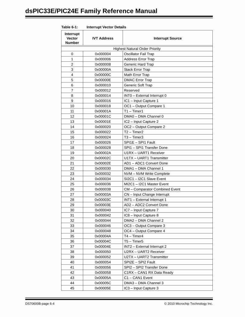
Table 6-1: Interrupt Vector Details
Interrupt Vector
NumberIVT Address Interrupt Source
Highest Natural Order Priority0 0x000004 Oscillator Fail Trap1 0x000006 Address Error Trap2 0x000008 Generic Hard Trap3 0x00000A Stack Error Trap4 0x00000C Math Error Trap5 0x00000E DMAC Error Trap6 0x000010 Generic Soft Trap7 0x000012 Reserved8 0x000014 INT0 – External Interrupt 09 0x000016 IC1 – Input Capture 110 0x000018 OC1 – Output Compare 111 0x00001A T1 – Timer112 0x00001C DMA0 – DMA Channel 013 0x00001E IC2 – Input Capture 214 0x000020 OC2 – Output Compare 215 0x000022 T2 – Timer216 0x000024 T3 – Timer317 0x000026 SPI1E – SPI1 Fault18 0x000028 SPI1 – SPI1 Transfer Done19 0x00002A U1RX – UART1 Receiver20 0x00002C U1TX – UART1 Transmitter21 0x00002E AD1 – ADC1 Convert Done22 0x000030 DMA1 – DMA Channel 123 0x000032 NVM – NVM Write Complete24 0x000034 SI2C1 – I2C1 Slave Event25 0x000036 MI2C1 – I2C1 Master Event26 0x000038 CM – Comparator Combined Event27 0x00003A CN – Input Change Interrupt28 0x00003C INT1 – External Interrupt 129 0x00003E AD2 – ADC2 Convert Done30 0x000040 IC7 – Input Capture 731 0x000042 IC8 – Input Capture 832 0x000044 DMA2 – DMA Channel 233 0x000046 OC3 – Output Compare 334 0x000048 OC4 – Output Compare 435 0x00004A T4 – Timer436 0x00004C T5 – Timer537 0x00004E INT2 – External Interrupt 238 0x000050 U2RX – UART2 Receiver39 0x000052 U2TX – UART2 Transmitter40 0x000054 SPI2E – SPI2 Fault41 0x000056 SPI2 – SPI2 Transfer Done42 0x000058 C1RX – CAN1 RX Data Ready43 0x00005A C1 – CAN1 Event44 0x00005C DMA3 – DMA Channel 345 0x00005E IC3 – Input Capture 3
DS70600B-page 6-4 © 2010 Microchip Technology Inc.

Section 6. InterruptsInterrupts
6
46 0x000060 IC4 – Input Capture 447 0x000062 IC5 – Input Capture 548 0x000064 IC6 – Input Capture 649 0x000066 OC5 – Output Compare 550 0x000068 OC6 – Output Compare 651 0x00006A OC7 – Output Compare 752 0x00006C OC8 – Output Compare 853 0x00006E PMP – Parallel Master Port54 0x000070 DMA4 – DMA Channel 455 0x000072 T6 – Timer656 0x000074 T7 – Timer757 0x000076 SI2C2 – I2C2 Slave Event58 0x000078 MI2C2 – I2C2 Master Event59 0x00007A T8 – Timer860 0x00007C T9 – Timer961 0x00007E INT3 – External Interrupt 362 0x000080 INT4 – External Interrupt 463 0x000082 C2RX – CAN2 RX Data Ready64 0x000084 C2 – CAN2 Event65 0x000086 PSEM – PWM Special Event Match66 0x000088 QEI1 – QEI1 Position Counter Compare67 0x00008A DCIE – DCI Fault Interrupt68 0x00008C DCI – DCI Transfer Done69 0x00008E DMA5 – DMA Channel 570 0x000090 RTC – Real-Time Clock and Calendar71 0x000092 Reserved72 0x000094 Reserved73 0x000096 U1E – UART1 Error Interrupt74 0x000098 U2E – UART2 Error Interrupt75 0x00009A CRC – CRC Generator Interrupt76 0x00009C DMA6 – DMA Channel 677 0x00009E DMA7 – DMA Channel 778 0x0000A0 C1TX – CAN1 TX Data Request79 0x0000A2 C2TX – CAN2 TX Data Request80 0x0000A4 Reserved81 0x0000A6 PSESM – PWM Secondary Special Event Match82 0x0000A8 Reserved83 0x0000AA QEI2 – QEI2 Position Counter Compare
84-91 0x0000AC-0x0000B4 Reserved92 0x0000B6 U3E – UART3 Error Interrupt93 0x0000B8 U3RX – UART3 Receiver94 0x0000BA U3TX – UART3 Transmitter95 0x0000BC Reserved96 0x0000BE Reserved97 0x0000C0 USB1 – USB OTG Interrupt98 0x0000C2 U4E – UART4 Error Interrupt99 0x0000C4 U4RX – UART4 Receiver
Table 6-1: Interrupt Vector Details (Continued)
Interrupt Vector
NumberIVT Address Interrupt Source
© 2010 Microchip Technology Inc. DS70600B-page 6-5

dsPIC33E/PIC24E Family Reference Manual
100 0x0000C6 U4TX – UART4 Transmitter101 0x0000C8 SPI3E – SPI3 Fault102 0x0000CA SPI3 – SPI3 Transfer Done103 0x0000CC OC9 – Output Compare 9104 0x0000CE IC9 – Input Capture 9105 0x0000D0 PWM1 – PWM Generator 1106 0x0000D2 PWM2 – PWM Generator 2107 0x0000D4 PWM3 – PWM Generator 3108 0x0000D6 PWM4 – PWM Generator 4109 0x0000D8 PWM5 – PWM Generator 5110 0x0000DA PWM6 – PWM Generator 6111 0x0000DC PWM7 – PWM Generator 7
112 -129 0x0000DE-0x0000FE Reserved130 0x000100 DMA8 – DMA Channel 8131 0x000102 DMA9 – DMA Channel 9132 0x000104 DMA10 – DMA Channel 10133 0x000106 DMA11 – DMA Channel 11134 0x000108 SPI4E – SPI4 Fault135 0x00010A SPI4 – SPI4 Transfer Done136 0x00010C OC10 – Output Compare 10137 0x00010E IC10 – Input Capture 10138 0x000110 OC11 – Output Compare11139 0x000112 IC11 – Input Capture 11140 0x000114 OC12 – Output Compare12141 0x000116 IC12 – Input Capture 12142 0x000118 DMA12 – DMA Channel 12143 0x00011A DMA13– DMA Channel 13144 0x00011C DMA14 – DMA Channel 14145 0x00011E Reserved146 0x000120 OC13 – Output Compare 13147 0x000122 IC13 – Input Capture 13148 0x000124 OC14 – Output Compare14149 0x000126 IC14 – Input Capture 14150 0x000128 OC15 – Output Compare15151 0x00012A IC15 – Input Capture 15152 0x00012C OC16 – Output Compare 16153 0x00012E IC16 – Input Capture 16154 0x000130 ICD – ICD Application
155-359 0x000132-0x0001FE ReservedLowest Natural Order Priority
Table 6-1: Interrupt Vector Details (Continued)
Interrupt Vector
NumberIVT Address Interrupt Source
DS70600B-page 6-6 © 2010 Microchip Technology Inc.

Section 6. InterruptsInterrupts
6
6.1.3 CPU Priority StatusThe CPU can operate at one of the 16 priority levels that range from 0-15. An interrupt or a trapsource must have a priority level greater than the current CPU priority to initiate an exceptionprocess. Peripherals and external interrupt sources can be programmed to level 0-7. CPU prioritylevels 8-15 are reserved for trap sources.A trap is a non-maskable interrupt source intended to detect hardware and software problems(see 6.2 “Non-Maskable Traps”). The priority level for each trap source is fixed. Only one trapis assigned to a priority level. An interrupt source programmed to priority level 0 is effectivelydisabled because it can never be greater than the CPU priority.
The current CPU priority level is indicated by the following status bits:
• CPU Interrupt Priority Level (IPL<2:0>) status bits in the CPU Status Register (SR<7:5>)• CPU Interrupt Priority Level 3 (IPL3) status bit in the Core Control register (CORCON<3>)
The IPL<2:0> status bits are readable and writable, so the user application can modify these bitsto disable all sources of interrupts below a given priority level. For example, if IPL<2:0> = 3, theCPU would not be interrupted by any source with a programmed priority level of 0, 1, 2 or 3.
Trap events have higher priority than any user interrupt source. When the IPL3 bit is set, a trapevent is in progress. The IPL3 bit can be cleared, but not set, by the user application. In someapplications, the IPL3 bit will need to be cleared when a trap has occurred and branch to aninstruction other than the instruction immediately after the one that originally caused the trap tooccur. All user interrupt sources can be disabled by setting IPL<2:0> = 111.
6.1.4 Interrupt PriorityEach peripheral interrupt source can be assigned to one of the seven priority levels. The userassignable interrupt priority control bits for each individual interrupt are located in the leastsignificant three bits of each nibble within the IPCx registers. Bit 3 of each nibble is not used andis read as a ‘0’. These bits define the priority level assigned to a particular interrupt. The usablepriority levels are 1 (lowest priority) through 7 (highest priority). If all the IPC bits associated withan interrupt source are cleared, the interrupt source is effectively disabled.
More than one interrupt request source can be assigned to a specific priority level. To resolvepriority conflicts within a given user-assigned level, each source of an interrupt has a naturalpriority order based on its location in the IVT. Table 6-1 shows the location of each interruptsource in the IVT. The lower numbered interrupt vectors have higher natural priority, while thehigher numbered vectors have lower natural priority. The overall priority level for any pendingsource of an interrupt is first determined by the user application-assigned priority of that sourcein the IPCx register, then by the natural order priority within the IVT.
Natural order priority is used only to resolve conflicts between simultaneous pending interruptswith the same user application-assigned priority level. Once the priority conflict is resolved andthe exception process begins, the CPU can be interrupted only by a source with higheruser application-assigned priority. Interrupts with the same user application-assigned priority, buta higher natural order priority that become pending during the exception process, remainpending until the current exception process completes.
Each interrupt source can be assigned to one of seven priority levels. This enables the userapplication to assign a low natural order priority and a very high overall priority level to an interrupt.For example, the UART1 RX Interrupt can be assigned to priority level 7, and the External Interrupt0 (INT0) can be assigned to priority level 1, thus giving it a very low effective priority.
Note: The peripherals and sources of interrupt available in the IVT vary depending on thespecific dsPIC33E/PIC24E device. The sources of interrupt shown in this documentrepresent a comprehensive listing of all interrupt sources found ondsPIC33E/PIC24E devices. Refer to the specific device data sheet for furtherdetails.
© 2010 Microchip Technology Inc. DS70600B-page 6-7

dsPIC33E/PIC24E Family Reference Manual
6.2 NON-MASKABLE TRAPSTraps are non-maskable, nestable interrupts that adhere to a fixed priority structure. Trapsprovide a means to correct erroneous operation during debugging and the operation of theapplication. If the user application does not intend to correct a trap error condition, these vectorsmust be loaded with the address of a software routine to reset the device. Otherwise, the userapplication programs the trap vector with the address of a service routine that corrects the trapcondition.
The dsPIC33E/PIC24E consists of the following implemented sources of non-maskable traps:
• Oscillator Failure Trap• Stack Error Trap• Address Error Trap• Math Error Trap• DMAC Error Trap• Generic Hard Trap• Generic Soft Trap
For many of the trap conditions, the instruction that caused the trap is allowed to complete beforeexception processing begins. Therefore, the user application may have to correct the action ofthe instruction that caused the trap.
Each trap source has a fixed priority as defined by its position in the IVT. An oscillator failure traphas the highest priority, while a DMA Controller (DMAC) error trap has the lowest priority (seeFigure 6-1). In addition, trap sources are classified into two distinct categories: soft traps andhard traps.
6.2.1 Soft TrapsThe DMAC error trap (priority level 10), math error trap (priority level 11) and stack error trap(priority level 12) are categorized as soft trap sources. Soft traps can be treated likenon-maskable sources of an interrupt that adhere to the priority assigned by their position in theIVT. Soft traps are processed like interrupts and require two cycles to be sampled andacknowledged prior to exception processing. Therefore, additional instructions may be executedbefore a soft trap is acknowledged.
6.2.1.1 STACK ERROR TRAP (SOFT TRAP, LEVEL 12)
The stack is initialized to 0x1000 during a Reset. A stack error trap is generated if the StackPointer address is less than 0x1000.
A Stack Limit (SPLIM) register associated with the Stack Pointer is uninitialized at Reset. Thestack overflow check is not enabled until a word is written to the SPLIM register.
All Effective Addresses (EAs) generated using W15 as a source or destination pointer arecompared against the value in the SPLIM register. If the EA is greater than the contents of theSPLIM register, a stack error trap is generated. In addition, a stack error trap is generated if theEA calculation wraps over the end of data space (0xFFFF).
A stack error can be detected in software by polling the Stack Error Trap (STKERR) status bit(INTCON1<2>). To avoid re-entry into the Trap Service Routine (TSR), the STKERR status flagmust be cleared in software.
6.2.1.2 MATH ERROR TRAP (SOFT TRAP, LEVEL 11)
Any of the following events can generate a math error trap:
• Accumulator A overflow • Accumulator B overflow• Catastrophic accumulator overflow• Divide-by-zero• Shift Accumulator (SFTAC) operation that exceeds ±16 bits
DS70600B-page 6-8 © 2010 Microchip Technology Inc.

Section 6. InterruptsInterrupts
6
The following three bits in the INTCON1 register enable three types of accumulator overflowtraps:• The Accumulator A Overflow Trap Flag (OVATE) control bit (INTCON1<10>) enables traps for an Accumulator A overflow event.
• The Accumulator B Overflow Trap Flag (OVBTE) control bit (INTCON1<9>) enables traps for an Accumulator B overflow event.
• The Catastrophic Overflow Trap Enable (COVTE) control bit (INTCON1<8>) enables traps for a catastrophic overflow of either accumulator. When this trap is detected, these corresponding ERROR bits are set in the INTCON1 register:- Accumulator A Overflow Trap Flag (OVAERR)- Accumulator B Overflow Trap Flag (OVBERR)- Accumulator A Catastrophic Overflow Trap Enable (COVAERR)- Accumulator B Catastrophic Overflow Trap Enable (COVBERR)
An Accumulator A or Accumulator B overflow event is defined as a carry-out from bit 31. Theaccumulator overflow cannot occur if the 31-bit Saturation mode is enabled for the accumulator.A catastrophic accumulator overflow is defined as a carry-out from bit 39 of either accumulator.The catastrophic overflow cannot occur if accumulator saturation (31-bit or 39-bit) is enabled.
Divide-by-zero traps cannot be disabled. The divide-by-zero check is performed during the firstiteration of the REPEAT loop that executes the divide instruction. The Divide-by-zero Error Status(DIV0ERR) bit (INTCON1<6>) is set when this trap is detected.
Accumulator shift traps cannot be disabled. The SFTAC instruction can be used to shift theaccumulator by a literal value or a value in one of the W registers. If the shift value exceeds±16 bits, an arithmetic trap is generated and the Shift Accumulator Error Status (SFTACERR) bit(INTCON1<7>) is set. The SFTAC instruction executes, but the results of the shift are not writtento the target accumulator.
A math error trap can be detected in software by polling the Math Error Status (MATHERR) bit(INTCON1<4>). To avoid re-entry into the Trap Service Routine, the MATHERR status flag mustbe cleared in software. Before the MATHERR status bit can be cleared, all conditions that causedthe trap to occur must also be cleared. If the trap was due to an accumulator overflow, theAccumulator Overflow (OA and OB) status bits (SR<15:14>) must be cleared.
6.2.1.3 DMAC ERROR TRAP (SOFT TRAP, LEVEL 10)
A DMAC error trap occurs with these conditions:
• RAM write collision• DMA-ready peripheral RAM write collision
Write collision errors are a serious enough threat to system integrity to warrant a non-maskableCPU trap event. If both the CPU and a DMA channel attempt to write to a target address, theCPU is given priority and the DMA write is ignored. In this case, a DMAC error trap is generatedand the DMAC Error Status (DMACERR) bit (INTCON1<5>) is set.
6.2.1.4 GENERIC SOFT TRAP
A generic soft trap occurs when any of the bits within the INTCON3 register is set. Each bit withinthe INTCON3 register is assigned to a specific trap error condition.
6.2.1.4.1 USB Address Error Soft Trap (UAE)All USB endpoints are implemented as buffers in RAM. The CPU and the USB module both haveaccess to the buffers.
The application specifies the location of the endpoint buffers and other data through an endpointBuffer Descriptor Table (BDT). The size of the endpoint BDT is 512 bytes. The endpoint BDTcontains entries called endpoint buffer descriptors for each endpoint. Space for the endpointbuffer descriptor is allocated regardless of the endpoint enable/disable status.
The start address of the endpoint BDT is specified by the application. This 32-bit address shouldbe aligned at the 512 byte boundary (i.e., the last nine bits of the address should be zero) and isspecified in the UxBDTP1, UxBDTP2 and UxBDTP3 registers.
© 2010 Microchip Technology Inc. DS70600B-page 6-9

dsPIC33E/PIC24E Family Reference Manual
If the UxBDTP1, UxBDTP2, and UxBDTP3 registers are initialized pointing to unimplementedmemory or any of the 512 bytes of the buffer, this results in an unimplemented memory accessby the USB module, and a USB Address Error Soft Trap will be issued, and UAE bit will be set.Refer to Section 25. “USB On-The-Go (OTG)” (DS70175) for additional information.
6.2.1.4.2 DMA Address Error Soft Trap (DAE)The Direct Memory Access (DMA) controller transfers data between peripheral data registersand data space SRAM. If the DMA module attempts to access any unimplemented memoryaddress, a DMA Address Error Soft Trap will be issued, and the DAE bit will be set. Refer toSection 22. “Direct Memory Access (DMA)” (DS70348) for additional information.
6.2.1.4.3 DO Stack Overflow Soft Trap (DOOVR)Up to 4 levels of DO loops can be executed and nested in hardware. The DO Level bits DL<2:0>in the CORCON register indicate the DO nesting level and used to address the DO Stack. Theyare automatically updated for all nested DO loops. A DO level of 0 (DL<2:0> = 000) indicates thatno DO loops are nested (i.e., no DO state needs to be preserved). A DO level of 4 (DL<2:0> = 100)indicates that four prior DO loops are in progress and nested.
If the user attempts to nest a DO loop when the DO stack is already full (DL<2:0> = 100, or 4 DOloops already underway), a DO Stack Overflow Soft Trap will be issued (DOOVR = 1). The DOinstruction that caused the trap will not change any of the DO states prior to the instructionexecution, nor will it modify the DO stack. The user may choose to try and recover the Faultcondition, abort the task or just Reset the device.
6.2.2 Hard TrapsHard traps include exceptions of priority level 13 through level 15, inclusive. The address error(level 13) and oscillator error (level 14) traps fall into this category.
Like soft traps, hard traps are non-maskable sources of interrupt. The difference between hardtraps and soft traps is that hard traps force the CPU to stop code execution after the instructioncausing the trap has completed. Normal program execution flow does not resume until the traphas been acknowledged and processed.
6.2.2.1 TRAP PRIORITY AND HARD TRAP CONFLICTS
If a higher priority trap occurs while any lower priority trap is in progress, the processing of thelower priority trap is suspended. The higher priority trap is acknowledged and processed. Thelower priority trap remains pending until the processing of the higher priority trap completes.
Each hard trap that occurs must be acknowledged before code execution of any type cancontinue. If a lower priority hard trap occurs while a higher priority trap is pending, acknowledgedor is being processed, a hard trap conflict occurs because the lower priority trap cannot beacknowledged until the processing for the higher priority trap completes.
The device is automatically Reset in a hard trap conflict condition. The Trap Reset Flag (TRAPR)status bit in the Reset Control Register (RCON<15>) is set when the Reset occurs so that thecondition can be detected in software. For further details, refer to Section 8. “Reset” (DS70602).
6.2.2.2 OSCILLATOR FAILURE TRAP (HARD TRAP, LEVEL 14)
An oscillator failure trap event is generated for any of these reasons:
• The Fail-Safe Clock Monitor (FSCM) is enabled and has detected a loss of the system clock source.
• A loss of PLL lock has been detected during normal operation using the PLL.• The FSCM is enabled and the PLL fails to achieve lock at a Power-on Reset (POR).
An oscillator failure trap event can be detected in software by polling the Oscillator Failure Trap(OSCFAIL) status bit (INTCON1<1>) or the Clock Fail (CF) status bit (OSCCON<3>). To avoidre-entry into the Trap Service Routine, the OSCFAIL status flag must be cleared in software. Formore information about the Fail-Safe Clock Monitor, refer to Section 7. “Oscillator” (DS70580) andSection 30. “Device Configuration” (DS70618).
DS70600B-page 6-10 © 2010 Microchip Technology Inc.

Section 6. InterruptsInterrupts
6
6.2.2.3 ADDRESS ERROR TRAP (HARD TRAP, LEVEL 13)Operating conditions that can generate an address error trap include the following:
• A misaligned data word fetch is attempted. This condition occurs when an instruction performs a word access with the Least Significant bit (LSb) of the effective address set to ‘1’. The dsPIC33E/PIC24E CPU requires all word accesses to be aligned to an even address boundary.
• A bit manipulation instruction uses the Indirect Addressing mode with the LSb of the effective address set to ‘1’.
• A data fetch is attempted from unimplemented data address space.• Execution of a BRA #literal instruction or a GOTO #literal instruction, where literal is an unimplemented program memory address.
• A data read or write is attempted with paged addressing when the dsr/dsw page is 0.• Execution of instructions after the PC has been modified to point to unimplemented
program memory addresses. The PC can be modified by loading a value into the stack and executing a RETURN instruction.
When an address error trap occurs, data space writes are inhibited so that data is not destroyed.
An address error can be detected in software by polling the ADDRERR status bit (INTCON1<3>).To avoid re-entry into the Trap Service Routine, the ADDRERR status flag must be cleared insoftware.
6.2.2.4 GENERIC HARD TRAP
A generic hard trap occurs when the following occurs:
• The SWTRAP bit in the (INTCON2<13>) register is set• Any bit within the INTCON4 register is set
6.2.3 Disable Interrupts InstructionThe DISI (Disable Interrupts) instruction can disable interrupts for up to 16384 instruction cycles.This instruction is useful for executing time-critical code segments.
The DISI instruction only disables interrupts with priority levels 1-6. Priority level 7 interrupts andall trap events can still interrupt the CPU when the DISI instruction is active.
The DISI instruction works in conjunction with the Disable Interrupts Count (DISICNT) registerin the CPU. When the DISICNT register is non-zero, priority level 1-6 interrupts are disabled. TheDISICNT register is decremented on each subsequent instruction cycle. When the DISICNTregister counts down to zero, priority level 1-6 interrupts are re-enabled. The value specified inthe DISI instruction includes all cycles due to PSV accesses, instruction stalls, and so on.
The DISICNT register is both readable and writable. The user application can terminate the effectof a previous DISI instruction early by clearing the DISICNT register. The duration for which theinterrupts are disabled can also be increased by writing to or adding to the DISICNT register.
If the DISICNT register is zero, interrupts cannot be disabled by simply writing a non-zero valueto the register. Interrupts must first be disabled by using the DISI instruction. Once the DISIinstruction has executed and DISICNT holds a non-zero value, the application can extend theinterrupt disable time by modifying the contents of the DISICNT register.
The DISI Instruction (DISI) status bit (INTCON2<14>) is set whenever interrupts are disabledas a result of the DISI instruction.
Note: In the MAC class of instructions, the data space is split into X and Y spaces. In theseinstructions, unimplemented X space includes all of Y space, and unimplemented Yspace includes all of X space.
Note: If the SWTRAP bit (INTCON2<13> is set to ‘1’ by the user, the SGHT bit(INTCON4<0>) is automatically set to ‘1’, which causes code execution to enter thegeneric hard trap handler. Both the SWTRAP and SGHT bits should be cleared (i.e.,set to ‘0’) in the trap handler to avoid repetitive traps.
Note: The DISI instruction can be used to quickly disable all user interrupt sources if nosource is assigned to CPU priority level 7.
© 2010 Microchip Technology Inc. DS70600B-page 6-11

dsPIC33E/PIC24E Family Reference Manual
6.2.3.1 GLOBAL INTERRUPT ENABLE (GIE)
A Global Interrupt Enable (GIE) control bit is used to enable or disable all interrupts globally.When the GIE bit is cleared, it causes the interrupt controller to behave as if the CPU’s IPL bitsare set to 7 (see Register 6-1) and disables all interrupts except the traps. When the GIE bit isset again, the interrupt controller acts based on the IPL value and the system will return to theprevious operating state, depending on the prior interrupt priority bit settings.
6.2.4 Interrupt OperationAll interrupt event flags are sampled during each instruction cycle. A pending Interrupt Request(IRQ) is indicated by the flag bit = 1 in an IFSx register. The IRQ causes an interrupt if thecorresponding bit in the Interrupt Enable (IECx) registers is set. During the rest of the instructioncycle in which the IRQ is sampled, the priorities of all pending interrupt requests are evaluated.
No instruction is aborted when the CPU responds to the IRQ. When the IRQ is sampled, theinstruction in progress is completed before the Interrupt Service Routine (ISR) is executed.
If there is a pending IRQ with a user application-assigned priority level greater than the currentprocessor priority level, indicated by the IPL<2:0> status bits (SR<7:5>), an interrupt is presentedto the processor. The processor then saves the following information on the software stack:
• Current PC value• Low byte of the Processor Status register (SRL)• IPL3 status bit (CORCON<3>)• Stack Frame Active (CORCON<3>)
These three values allow the return PC address value, MCU status bits and current processorpriority level to be automatically saved.
After this information is saved on the stack, the CPU writes the priority level of the pendinginterrupt into the IPL<2:0> bit locations. This action disables all interrupts of lower or equalpriority until the ISR is terminated using the RETFIE instruction.
Figure 6-2: Stack Operation for Interrupt Event
6.2.4.1 RETURN FROM INTERRUPT
The RETFIE (Return from Interrupt) instruction unstacks the PC return address, IPL3 status bit,SFA bit and SRL register to return the processor to the state and priority level that existed beforethe interrupt sequence.
Note: The GIE bit does not modify the CPU’s IPL bits.
<Free Word>
PC<15:1>; PC<22:16>
015
W15 (before IRQ)
W15 (after IRQ)
Stac
k G
row
s To
war
dH
ighe
r Add
ress
SR<7:0>
This stack storesthe IPL3 statusbit (CORCON<3>)
This stack stores the SFA bit (CORCON<2>)
DS70600B-page 6-12 © 2010 Microchip Technology Inc.
Section 6. InterruptsInterrupts
6
6.2.4.2 INTERRUPT NESTINGInterrupts are nestable by default. Any ISR in progress can be interrupted by another source ofinterrupt with a higher user application-assigned priority level. Interrupt nesting can be disabledby setting the Interrupt Nesting Disable (NSTDIS) control bit (INTCON1<15>). When the NSTDIScontrol bit is set, all interrupts in progress force the CPU priority to level 7 by settingIPL<2:0> = 111. This action effectively masks all other sources of interrupt until a RETFIEinstruction is executed. When interrupt nesting is disabled, the user application-assignedinterrupt priority levels have no effect except to resolve conflicts between simultaneous pendinginterrupts.
The IPL<2:0> bits (SR<7:5>) become read-only when interrupt nesting is disabled. This preventsthe user application from setting IPL<2:0> to a lower value, which would effectively re-enableinterrupt nesting.
6.2.5 Wake-up from Sleep and IdleAny source of interrupt that is individually enabled using its corresponding control bit in the IECxregisters, can wake-up the processor from Sleep or Idle mode. When the interrupt status flag fora source is set and the interrupt source is enabled by the corresponding bit in the IEC Controlregisters, a wake-up signal is sent to the dsPIC33E/PIC24E CPU. When the device wakes fromSleep or Idle mode, one of two actions occur:
• If the interrupt priority level for that source is greater than the current CPU priority level, the processor will process the interrupt and branch to the ISR for the interrupt source.
• If the user application-assigned interrupt priority level for the source is lower than or equal to the current CPU priority level, the processor will continue execution, starting with the instruction immediately following the PWRSAV instruction that previously put the CPU in Sleep or Idle mode.
6.2.6 Analog-to-Digital Converter (ADC) External Conversion Request
The INT0 external interrupt request pin is shared with the ADC as an external conversion requestsignal. The INT0 interrupt source has programmable edge polarity, which is also available to theADC external conversion request feature.
6.2.7 External Interrupt SupportThe dsPIC33E/PIC24E supports up to five external interrupt pin sources (INT0-INT4). Eachexternal interrupt pin has edge detection circuitry to detect the interrupt event. The INTCON2register has five control bits (INT0EP-INT4EP) that select the polarity of the edge detectioncircuitry. Each external interrupt pin can be programmed to interrupt the CPU on a rising edge orfalling edge event. See Register 6-4 for further details.
Note: User interrupt sources that are assigned to CPU priority level 0 cannot wake theCPU from Sleep or Idle mode because the interrupt source is effectively disabled.To use an interrupt as a wake-up source, the program must assign the CPU prioritylevel for the interrupt to level 1 or greater.
© 2010 Microchip Technology Inc. DS70600B-page 6-13

dsPIC33E/PIC24E Family Reference Manual
6.3 INTERRUPT PROCESSING TIMING
6.3.1 Interrupt Latency for One-Cycle InstructionsFigure 6-3 illustrates the sequence of events when a peripheral interrupt is asserted during aone-cycle instruction. The interrupt process takes ten instruction cycles. Each cycle is numberedin the figure for reference.
During the instruction cycle, the interrupt flag status bit is set after the peripheral interrupt occurs.The current instruction completes during this instruction cycle. In the second instructioncycle after the interrupt event, the contents of the PC and Lower Byte Status (SRL) registers aresaved into a temporary buffer register. The second cycle of the interrupt process is executed asa NOP to maintain consistency with the sequence taken during a two-cycle instruction (see6.3.2 “Interrupt Latency for Two-Cycle Instructions”). In the third cycle, the PC is loaded withthe vector table address for the interrupt source and the starting address of the ISR is fetched.In the fourth cycle, the PC is loaded with the ISR address. The fourth cycle is executed as a NOPwhile the first instruction in the ISR is fetched.
Figure 6-3: Interrupt Timing During a One-Cycle Instruction
11
FNOP
1 2 3 4 5 86 7 9 10
INST INST FNOPFNOP FetchVector
FNOP FNOP FNOPFNOP FNOPISR
PC PC + 2 Vector # ISR
4 6 6 6 6 6CPU Priority
Interrupt FlagStatus bit
INST Executed
44
12 13
6
ISR
14
6
PUSH Low 16 bits of PCPUSH SRL and High 8 bits of PCSave PC in
Peripheral interrupt eventoccurs at or before midpoint
temporarybuffer
of this cycle
(from temporary buffer)(from temporary buffer)
(PC - 2)
4 444
Fetch(PC)
DS70600B-page 6-14 © 2010 Microchip Technology Inc.

Section 6. InterruptsInterrupts
6
6.3.2 Interrupt Latency for Two-Cycle InstructionsThe interrupt latency during a two-cycle instruction is the same as during a one-cycle instruction.The first and second cycle of the interrupt process allow the two-cycle instruction to completeexecution. The timing diagram in Figure 6-4 illustrates the peripheral interrupt event occurring inthe instruction cycle prior to execution of the two-cycle instruction.Figure 6-5 illustrates the timing when a peripheral interrupt coincides with the first cycle of atwo-cycle instruction. In this case, the interrupt process completes as for a one-cycle instruction(see 6.3.1 “Interrupt Latency for One-Cycle Instructions”).
Figure 6-4: Interrupt Timing During a Two-Cycle Instruction
Figure 6-5: Interrupt Timing, Interrupt Occurs During 1st Cycle of a Two-Cycle Instruction
11
FNOP
1 2 3 4 5 86 7 9 10
FNOPFNOP FetchVector
FNOP FNOPFNOP FNOPISR
PC PC + 2 Vector # ISR
4 6 6 6 6 6CPU Priority
Interrupt FlagStatus bit
INST Executed
44
12 13
6
ISR
14
6
PUSH Low 16 bits of PCPUSH SRL and High 8 bits of PCSave PC in
Peripheral interrupt eventoccurs at or before midpoint
temporarybuffer
of this cycle
(from temporary buffer)(from temporary buffer)
4 444
FetchINST 1st
Cycle
INST2nd
Cycle
INST (PC - 2)
11
FNOP
1 2 3 4 5 86 7 9 10
FNOPFNOP FetchVector
FNOP FNOPFNOP FNOPISR
PC PC + 2 Vector # ISR
4 6 6 6 6 6CPU Priority
Interrupt FlagStatus bit
INST Executed
44
12 13
6
ISR
14
6
PUSH Low 16 bits of PCPUSH SRL and High 8 bits of PCSave PC in
Peripheral interrupt eventoccurs at or before midpoint
temporarybuffer
of this cycle
(from temporary buffer)(from temporary buffer)
4 444
FetchINST 1st
INST2nd
Cycle
INST (PC-2)
ISR + 2
Cycle
© 2010 Microchip Technology Inc. DS70600B-page 6-15

dsPIC33E/PIC24E Family Reference Manual
6.3.3 Returning from InterruptTo return from an interrupt, the program must call the RETFIE instruction.
During the first two cycles of a RETFIE instruction, the contents of the PC and the SRL registerare popped from the stack. The third instruction cycle is used to fetch the instruction addressedby the updated program counter. This cycle executes as a NOP instruction. On the fourth cycle,program execution resumes at the point where the interrupt occurred.
Figure 6-6: Return from Interrupt Timing
6.3.4 Exception LatencyThe interrupt latency can be selected as a fixed latency or variable latency. An exception processcan operate in one of two modes. It is determined by the state of the VAR bit in the Core Control(CORCON<15>) register.
6.3.4.1 FIXED LATENCY (VAR = 0 AND CPU HIGHEST PRIORITY MASTER)
If VAR = 0 (default Reset state) and the CPU is the highest priority EDS bus master(MSTRPR<2:0> = 000), the CPU offers a deterministic fixed latency response to any highestpriority exception. The interrupt latency, which is a time interval between the instance wheninterrupt is recognized and the instance when the first instruction of the ISR is executed, remainsunchanged for all instructions including a TBLRDx instruction, or instructions that require PSVaccess.
When the following occurs, the interrupt latency time is not fixed:
• The MOV.D instruction accessing data via PSV adds one cycle to complete the second PSV fetch.
• A TBLRDx or PSV access instruction associated with a stall cycle adds one cycle. • Last iteration of a repeated PSV access adds one cycle.
6.3.4.2 VARIABLE LATENCY (VAR = 1 AND CPU HIGHEST PRIORITY MASTER)
If VAR = 1 and the CPU is the highest priority EDS bus master (MSTRPR<2:0> = 000), the CPUoffers a variable latency response to all exceptions. If more than one interrupt is active, and thedevice is operating in Non-Nested mode, a higher priority interrupt request can occur when alower priority interrupt is being processed. Therefore, the time required to execute the longestISR must be added to the maximum latency.
If VAR = 0, the exception processing time requires 13 instruction cycle flash access time (i.e.,216 ns at a 60 MHz operating speed).
If VAR = 1, the exception processing time is variable and it requires 9-13 instruction cycle flashaccess time (i.e., 150 ns through 216 ns at a 60 MHz operating speed).
4 4 4 46 4CPU
Priority
RETFIE RETFIEINSTExecuted
FNOPISR last
6
ISR ISR + 2PC
2nd Cycle
TCY
instruction
1 2 3 4 5
FNOP FNOP
PC
6
4
PC
7
FNOP
DS70600B-page 6-16 © 2010 Microchip Technology Inc.

Section 6. InterruptsInterrupts
6
6.3.5 Special Conditions for Interrupt LatencyThe dsPIC33E/PIC24E allows the current instruction to complete when a peripheral interruptsource becomes pending. The interrupt latency is the same for both one-cycle and two-cycleinstructions. However, certain conditions can increase interrupt latency by one cycle, dependingon when the interrupt occurs. If a fixed latency is critical to the application, the followingconditions should be avoided:• A MOV.D instruction is executed that uses PSV to access a value in program memory space
• An instruction stall cycle is appended to any two-cycle instruction• An instruction stall cycle is appended to any one-cycle instruction that performs a PSV
access• A bit test and skip instruction (BTSC, BTSS) that uses PSV to access a value in the program
memory space
© 2010 Microchip Technology Inc. DS70600B-page 6-17

dsPIC33E/PIC24E Family Reference Manual
6.4 INTERRUPT CONTROL AND STATUS REGISTERSThe following registers are associated with the interrupt controller:
• INTCONx: Interrupt Control RegistersThese registers control global interrupt functions, where ‘x’ denotes the register number:
- INTCON1 contains the Interrupt Nesting Disable (NSTDIS) bit, as well as the control and status flags for the processor trap sources
- INTCON2 controls external interrupt request signal behavior and the use of the alternate vector table
- INTCON3 controls the soft trap status bits- INTCON4 controls software generated hard trap status bits
• IFSx: Interrupt Flag Status RegistersAll interrupt request flags are maintained in the IFSx registers, where ‘x’ denotes the registernumber. Each source of interrupt has a status bit, which is set by the respective peripheralsor external signals and cleared by software.
• IECx: Interrupt Enable Control RegistersAll Interrupt Enable Control bits are maintained in the IECx registers, where ‘x’ denotes theregister number. These control bits are used to individually enable interrupts from theperipherals or external signals.
• IPCx: Interrupt Priority Control RegistersEach user interrupt source can be assigned to one of eight priority levels. The IPC registersset the interrupt priority level for each source of interrupt.
• SR: Status Register (In CPU)The SR is not a specific part of the interrupt controller hardware; however, it contains theIPL<2:0> status bits (SR<7:5>), which indicate the current CPU priority level. The userapplication can change the current CPU priority level by writing to the IPL bits.
• CORCON: Core Control Register The CORCON register is not a specific part of the interrupt controller hardware; however, itcontains the IPL3 status bit, which indicates the current CPU priority level. IPL3 is aread-only bit so that trap events cannot be masked by the user application.
Each register is described in detail in the following sections.
6.4.1 Assignment of Interrupts to Control RegistersThe interrupt sources are assigned to the IFSx, IECx and IPCx registers in the same sequenceas they are listed in Table 6-1. For example, the INT0 (External Interrupt 0) source has a vectornumber and natural order priority of 0. Therefore, the External Interrupt 0 Flag Status (INT0IF)bit is found in IFS0<0>. The INT0 interrupt uses bit 0 of the IEC0 register as its Enable bit. TheIPC0<2:0> bits assign the interrupt priority level for the INT0 interrupt.
Note: The total number and type of interrupt sources depend on the device variant. Referto the specific device data sheet for further details.
DS70600B-page 6-18 © 2010 Microchip Technology Inc.

Section 6. InterruptsInterrupts
6
Register 6-1: SR: Status Register (In CPU)
R-0 R-0 R/C-0 R/C-0 R-0 R/C-0 R-0 R-0OA OB SA SB OAB SAB DA DC
bit 15 bit 8
R/W-0 R/W-0 R/W-0 R-0 R/W-0 R/W-0 R/W-0 R/W-0IPL<2:0>(1,2) RA N OV Z C
bit 7 bit 0
Legend: C = Bit can be clearedR = Readable bit W = Writable bit U = Unimplemented bit, read as ‘0’-n = Value at POR ‘1’ = Bit is set ‘0’ = Bit is cleared x = Bit is unknown
bit 15-8 Not used by the Interrupt Controller(Refer to Section 2. “CPU” (DS70359) for the SR bit descriptions)
bit 7-5 IPL<2:0>: CPU Interrupt Priority Level Status bits(1,2)
111 = CPU interrupt priority level is 7 (15). User interrupts disabled110 = CPU interrupt priority level is 6 (14)101 = CPU interrupt priority level is 5 (13)100 = CPU interrupt priority level is 4 (12)011 = CPU interrupt priority level is 3 (11)010 = CPU interrupt priority level is 2 (10)001 = CPU interrupt priority level is 1 (9)000 = CPU interrupt priority level is 0 (8)
bit 4-0 Not used by the Interrupt Controller(Refer to Section 2. “CPU” (DS70359) for the SR bit descriptions)
Note 1: The IPL<2:0> bits are concatenated with the IPL<3> bit (CORCON<3>) to form the CPU interrupt prioritylevel. The value in parentheses indicates the IPL if IPL<3> = 1.
2: The IPL<2:0> status bits are read-only when NSTDIS = 1 (INTCON1<15>).
© 2010 Microchip Technology Inc. DS70600B-page 6-19

dsPIC33E/PIC24E Family Reference Manual
Register 6-2: CORCON: Core Control Register
R/W-0 U-0 R/W-0 R/W-0 R/W-0 R-0 R-0 R-0VAR — US<1:0> EDT DL<2:0>
bit 15 bit 8
R/W-0 R/W-0 R/W-1 R/W-0 R/C-0 R-0 R/W-0 R/W-0SATA SATB SATDW ACCSAT IPL3(1) SFA RND IF
bit 7 bit 0
Legend: C = Bit can be clearedR = Readable bit W = Writable bit U = Unimplemented bit, read as ‘0’-n = Value at POR ‘1’ = Bit is set ‘0’ = Bit is cleared x = Bit is unknown
bit 15 VAR: Variable Exception Processing Latency Control bit1 = Variable exception processing latency0 = Fixed exception processing latency(Refer to 6.3.4 “Exception Latency” for more information)
bit 14-4 Not used by the Interrupt Controller(Refer to Section 2. “CPU” (DS70359) for the CORCON bit descriptions)
bit 3 IPL3: CPU Interrupt Priority Level Status bit 3(1)
1 = CPU interrupt priority level is greater than 70 = CPU interrupt priority level is 7 or less
bit 2-0 Not used by the Interrupt Controller(Refer to Section 2. “CPU” (DS70359) for the CORCON bit descriptions)
Note 1: The IPL3 bit is concatenated with the IPL<2:0> bits (SR<7:5>) to form the CPU interrupt priority level.
DS70600B-page 6-20 © 2010 Microchip Technology Inc.

Section 6. InterruptsInterrupts
6
Register 6-3: INTCON1: Interrupt Control Register 1
R/W-0 R/W-0 R/W-0 R/W-0 R/W-0 R/W-0 R/W-0 R/W-0NSTDIS OVAERR OVBERR COVAERR COVBERR OVATE OVBTE COVTE
bit 15 bit 8
R/W-0 R/W-0 R/W-0 R/W-0 R/W-0 R/W-0 R/W-0 U-0SFTACERR DIV0ERR DMACERR MATHERR ADDRERR STKERR OSCFAIL —
bit 7 bit 0
Legend:R = Readable bit W = Writable bit U = Unimplemented bit, read as ‘0’-n = Value at POR ‘1’ = Bit is set ‘0’ = Bit is cleared x = Bit is unknown
bit 15 NSTDIS: Interrupt Nesting Disable bit1 = Interrupt nesting is disabled0 = Interrupt nesting is enabled
bit 14 OVAERR: Accumulator A Overflow Trap Flag bit1 = Trap was caused by overflow of Accumulator A0 = Trap was not caused by overflow of Accumulator A
bit 13 OVBERR: Accumulator B Overflow Trap Flag bit1 = Trap was caused by overflow of Accumulator B0 = Trap was not caused by overflow of Accumulator B
bit 12 COVAERR: Accumulator A Catastrophic Overflow Trap Flag bit1 = Trap was caused by catastrophic overflow of Accumulator A0 = Trap was not caused by catastrophic overflow of Accumulator A
bit 11 COVBERR: Accumulator B Catastrophic Overflow Trap Flag bit1 = Trap was caused by catastrophic overflow of Accumulator B0 = Trap was not caused by catastrophic overflow of Accumulator B
bit 10 OVATE: Accumulator A Overflow Trap Enable bit1 = Trap overflow of Accumulator A0 = Trap is disabled
bit 9 OVBTE: Accumulator B Overflow Trap Enable bit1 = Trap overflow of Accumulator B0 = Trap is disabled
bit 8 COVTE: Catastrophic Overflow Trap Enable bit1 = Trap on catastrophic overflow of Accumulator A or B enabled0 = Trap is disabled
bit 7 SFTACERR: Shift Accumulator Error Status bit1 = Math error trap was caused by an invalid accumulator shift0 = Math error trap was not caused by an invalid accumulator shift
bit 6 DIV0ERR: Divide-by-zero Error Status bit1 = Divide-by-zero error trap was caused by a divide by zero0 = Divide-by-zero error trap was not caused by a divide by zero
bit 5 DMACERR: DMAC Error Trap Status bit1 = DMAC trap has occurred0 = DMAC trap has not occurred
bit 4 MATHERR: Math Error Status bit1 = Math error trap has occurred0 = Math error trap has not occurred
bit 3 ADDRERR: Address Error Trap Status bit1 = Address error trap has occurred0 = Address error trap has not occurred
© 2010 Microchip Technology Inc. DS70600B-page 6-21

dsPIC33E/PIC24E Family Reference Manual
bit 2 STKERR: Stack Error Trap Status bit1 = Stack error trap has occurred0 = Stack error trap has not occurred
bit 1 OSCFAIL: Oscillator Failure Trap Status bit1 = Oscillator failure trap has occurred0 = Oscillator failure trap has not occurred
bit 0 Unimplemented: Read as ‘0’
Register 6-3: INTCON1: Interrupt Control Register 1 (Continued)
DS70600B-page 6-22 © 2010 Microchip Technology Inc.
Section 6. InterruptsInterrupts
6
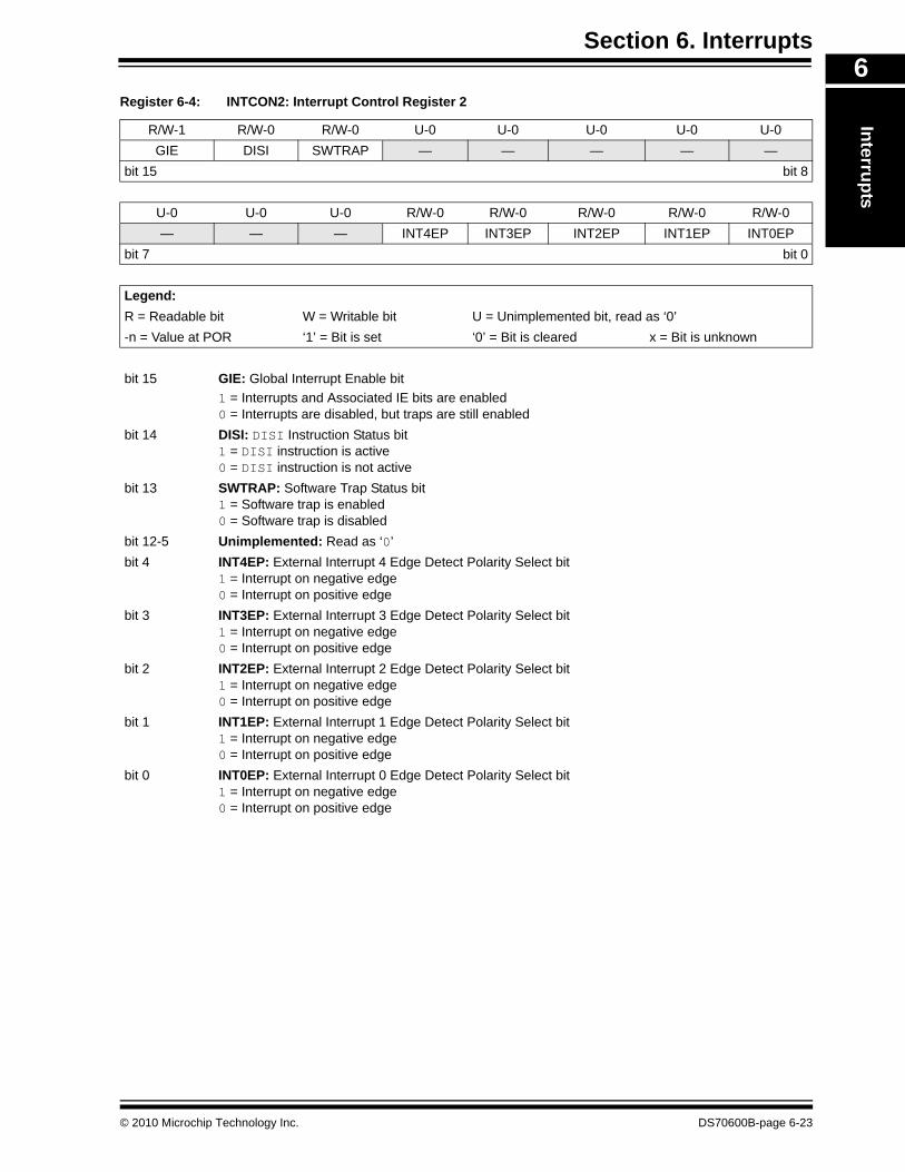
Register 6-4: INTCON2: Interrupt Control Register 2
R/W-1 R/W-0 R/W-0 U-0 U-0 U-0 U-0 U-0GIE DISI SWTRAP — — — — —
bit 15 bit 8
U-0 U-0 U-0 R/W-0 R/W-0 R/W-0 R/W-0 R/W-0— — — INT4EP INT3EP INT2EP INT1EP INT0EP
bit 7 bit 0
Legend:R = Readable bit W = Writable bit U = Unimplemented bit, read as ‘0’-n = Value at POR ‘1’ = Bit is set ‘0’ = Bit is cleared x = Bit is unknown
bit 15 GIE: Global Interrupt Enable bit1 = Interrupts and Associated IE bits are enabled 0 = Interrupts are disabled, but traps are still enabled
bit 14 DISI: DISI Instruction Status bit1 = DISI instruction is active0 = DISI instruction is not active
bit 13 SWTRAP: Software Trap Status bit1 = Software trap is enabled0 = Software trap is disabled
bit 12-5 Unimplemented: Read as ‘0’bit 4 INT4EP: External Interrupt 4 Edge Detect Polarity Select bit
1 = Interrupt on negative edge 0 = Interrupt on positive edge
bit 3 INT3EP: External Interrupt 3 Edge Detect Polarity Select bit1 = Interrupt on negative edge 0 = Interrupt on positive edge
bit 2 INT2EP: External Interrupt 2 Edge Detect Polarity Select bit1 = Interrupt on negative edge 0 = Interrupt on positive edge
bit 1 INT1EP: External Interrupt 1 Edge Detect Polarity Select bit1 = Interrupt on negative edge 0 = Interrupt on positive edge
bit 0 INT0EP: External Interrupt 0 Edge Detect Polarity Select bit1 = Interrupt on negative edge 0 = Interrupt on positive edge
© 2010 Microchip Technology Inc. DS70600B-page 6-23

dsPIC33E/PIC24E Family Reference Manual
Register 6-5: INTCON3: Interrupt Control Register 3
U-0 U-0 U-0 U-0 U-0 U-0 U-0 U-0— — — — — — — —
bit 15 bit 8
U-0 R/W-0 R/W-0 R/W-0 U-0 U-0 U-0 U-0— UAE DAE DOOVR — — — —
bit 7 bit 0
Legend:R = Readable bit W = Writable bit U = Unimplemented bit, read as ‘0’-n = Value at POR ‘1’ = Bit is set ‘0’ = Bit is cleared x = Bit is unknown
bit 15-7 Unimplemented: Read as ‘0’bit 6 UAE: USB Address Error Soft Trap Status bit
1 = USB address error (soft) trap has occurred0 = USB address error (soft) trap has not occurred
bit 5 DAE: DMA Address Error Soft Trap Status bit1 = DMA Address error soft trap has occurred0 = DMA Address error soft trap has not occurred
bit 4 DOOVR: Do Stack Overflow Soft Trap Status bit1 = Do stack overflow soft trap has occurred0 = Do stack overflow soft trap has not occurred
bit 3-0 Unimplemented: Read as ‘0’
DS70600B-page 6-24 © 2010 Microchip Technology Inc.

Section 6. InterruptsInterrupts
6
Register 6-6: INTCON4: Interrupt Control Register 4
U-0 U-0 U-0 U-0 U-0 U-0 U-0 U-0— — — — — — — —
bit 15 bit 8
U-0 U-0 U-0 U-0 U-0 U-0 U-0 R/W-0— — — — — — — SGHT
bit 7 bit 0
Legend:R = Readable bit W = Writable bit U = Unimplemented bit, read as ‘0’-n = Value at POR ‘1’ = Bit is set ‘0’ = Bit is cleared x = Bit is unknown
bit 15-1 Unimplemented: Read as ‘0’bit 0 SGHT: Software Generated Hard Trap Status bit
1 = Software generated hard trap has occurred0 = Software generated hard trap has not occurred
© 2010 Microchip Technology Inc. DS70600B-page 6-25

dsPIC33E/PIC24E Family Reference Manual
Register 6-7: IFS0: Interrupt Flag Status Register 0
R/W-0 R/W-0 R/W-0 R/W-0 R/W-0 R/W-0 R/W-0 R/W-0NVMIF DMA1IF AD1IF U1TXIF U1RXIF SPI1IF SPI1EIF T3IF
bit 15 bit 8
R/W-0 R/W-0 R/W-0 R/W-0 R/W-0 R/W-0 R/W-0 R/W-0T2IF OC2IF IC2IF DMA0IF T1IF OC1IF IC1IF INT0IF
bit 7 bit 0
Legend:R = Readable bit W = Writable bit U = Unimplemented bit, read as ‘0’-n = Value at POR ‘1’ = Bit is set ‘0’ = Bit is cleared x = Bit is unknown
bit 15 NVMIF: Non-Volatile Memory Interrupt Flag Status bit1 = Interrupt request has occurred0 = Interrupt request has not occurred
bit 14 DMA1IF: DMA Channel 1 Data Transfer Complete Interrupt Flag Status bit1 = Interrupt request has occurred0 = Interrupt request has not occurred
bit 13 AD1IF: ADC1 Conversion Complete Interrupt Flag Status bit1 = Interrupt request has occurred0 = Interrupt request has not occurred
bit 12 U1TXIF: UART1 Transmitter Interrupt Flag Status bit1 = Interrupt request has occurred0 = Interrupt request has not occurred
bit 11 U1RXIF: UART1 Receiver Interrupt Flag Status bit1 = Interrupt request has occurred0 = Interrupt request has not occurred
bit 10 SPI1IF: SPI1 Event Interrupt Flag Status bit1 = Interrupt request has occurred0 = Interrupt request has not occurred
bit 9 SPI1EIF: SPI1 Fault Interrupt Flag Status bit1 = Interrupt request has occurred0 = Interrupt request has not occurred
bit 8 T3IF: Timer3 Interrupt Flag Status bit1 = Interrupt request has occurred0 = Interrupt request has not occurred
bit 7 T2IF: Timer2 Interrupt Flag Status bit1 = Interrupt request has occurred0 = Interrupt request has not occurred
bit 6 OC2IF: Output Compare Channel 2 Interrupt Flag Status bit1 = Interrupt request has occurred0 = Interrupt request has not occurred
bit 5 IC2IF: Input Capture Channel 2 Interrupt Flag Status bit1 = Interrupt request has occurred0 = Interrupt request has not occurred
bit 4 DMA0IF: DMA Channel 0 Data Transfer Complete Interrupt Flag Status bit1 = Interrupt request has occurred0 = Interrupt request has not occurred
DS70600B-page 6-26 © 2010 Microchip Technology Inc.

Section 6. InterruptsInterrupts
6
bit 3 T1IF: Timer1 Interrupt Flag Status bit1 = Interrupt request has occurred0 = Interrupt request has not occurred
bit 2 OC1IF: Output Compare Channel 1 Interrupt Flag Status bit1 = Interrupt request has occurred0 = Interrupt request has not occurred
bit 1 IC1IF: Input Capture Channel 1 Interrupt Flag Status bit1 = Interrupt request has occurred0 = Interrupt request has not occurred
bit 0 INT0IF: External Interrupt 0 Flag Status bit1 = Interrupt request has occurred0 = Interrupt request has not occurred
Register 6-7: IFS0: Interrupt Flag Status Register 0 (Continued)
© 2010 Microchip Technology Inc. DS70600B-page 6-27

dsPIC33E/PIC24E Family Reference Manual
Register 6-8: IFS1: Interrupt Flag Status Register 1
R/W-0 R/W-0 R/W-0 R/W-0 R/W-0 R/W-0 R/W-0 R/W-0U2TXIF U2RXIF INT2IF T5IF T4IF OC4IF OC3IF DMA2IF
bit 15 bit 8
R/W-0 R/W-0 R/W-0 R/W-0 R/W-0 R/W-0 R/W-0 R/W-0IC8IF IC7IF AD2IF INT1IF CNIF CMIF MI2C1IF SI2C1IF
bit 7 bit 0
Legend:R = Readable bit W = Writable bit U = Unimplemented bit, read as ‘0’-n = Value at POR ‘1’ = Bit is set ‘0’ = Bit is cleared x = Bit is unknown
bit 15 U2TXIF: UART2 Transmitter Interrupt Flag Status bit1 = Interrupt request has occurred0 = Interrupt request has not occurred
bit 14 U2RXIF: UART2 Receiver Interrupt Flag Status bit1 = Interrupt request has occurred0 = Interrupt request has not occurred
bit 13 INT2IF: External Interrupt 2 Flag Status bit1 = Interrupt request has occurred0 = Interrupt request has not occurred
bit 12 T5IF: Timer5 Interrupt Flag Status bit1 = Interrupt request has occurred0 = Interrupt request has not occurred
bit 11 T4IF: Timer4 Interrupt Flag Status bit1 = Interrupt request has occurred0 = Interrupt request has not occurred
bit 10 OC4IF: Output Compare Channel 4 Interrupt Flag Status bit1 = Interrupt request has occurred0 = Interrupt request has not occurred
bit 9 OC3IF: Output Compare Channel 3 Interrupt Flag Status bit1 = Interrupt request has occurred0 = Interrupt request has not occurred
bit 8 DMA2IF: DMA Channel 2 Data Transfer Complete Interrupt Flag Status bit1 = Interrupt request has occurred0 = Interrupt request has not occurred
bit 7 IC8IF: Input Capture Channel 8 Interrupt Flag Status bit1 = Interrupt request has occurred0 = Interrupt request has not occurred
bit 6 IC7IF: Input Capture Channel 7 Interrupt Flag Status bit1 = Interrupt request has occurred0 = Interrupt request has not occurred
bit 5 AD2IF: ADC2 Conversion Complete Interrupt Flag Status bit1 = Interrupt request has occurred0 = Interrupt request has not occurred
bit 4 INT1IF: External Interrupt 1 Flag Status bit1 = Interrupt request has occurred0 = Interrupt request has not occurred
DS70600B-page 6-28 © 2010 Microchip Technology Inc.

Section 6. InterruptsInterrupts
6
bit 3 CNIF: Input Change Notification Interrupt Flag Status bit1 = Interrupt request has occurred0 = Interrupt request has not occurred
bit 2 CMIF: Comparator Interrupt Flag Status bit1 = Interrupt request has occurred0 = Interrupt request has not occurred
bit 1 MI2C1IF: I2C1 Master Events Interrupt Flag Status bit1 = Interrupt request has occurred0 = Interrupt request has not occurred
bit 0 SI2C1IF: I2C1 Slave Events Interrupt Flag Status bit1 = Interrupt request has occurred0 = Interrupt request has not occurred
Register 6-8: IFS1: Interrupt Flag Status Register 1 (Continued)
© 2010 Microchip Technology Inc. DS70600B-page 6-29

dsPIC33E/PIC24E Family Reference Manual
Register 6-9: IFS2: Interrupt Flag Status Register 2
R/W-0 R/W-0 R/W-0 R/W-0 R/W-0 R/W-0 R/W-0 R/W-0T6IF DMA4IF PMPIF OC8IF OC7IF OC6IF OC5IF IC6IF
bit 15 bit 8
R/W-0 R/W-0 R/W-0 R/W-0 R/W-0 R/W-0 R/W-0 R/W-0IC5IF IC4IF IC3IF DMA3IF C1IF C1RXIF SPI2IF SPI2EIF
bit 7 bit 0
Legend:R = Readable bit W = Writable bit U = Unimplemented bit, read as ‘0’-n = Value at POR ‘1’ = Bit is set ‘0’ = Bit is cleared x = Bit is unknown
bit 15 T6IF: Timer6 Interrupt Flag Status bit1 = Interrupt request has occurred0 = Interrupt request has not occurred
bit 14 DMA4IF: DMA Channel 4 Data Transfer Complete Interrupt Flag Status bit1 = Interrupt request has occurred0 = Interrupt request has not occurred
bit 13 PMPIF: Parallel Master Port Interrupt Flag Status bit1 = Interrupt request has occurred0 = Interrupt request has not occurred
bit 12 OC8IF: Output Compare Channel 8 Interrupt Flag Status bit1 = Interrupt request has occurred0 = Interrupt request has not occurred
bit 11 OC7IF: Output Compare Channel 7 Interrupt Flag Status bit1 = Interrupt request has occurred0 = Interrupt request has not occurred
bit 10 OC6IF: Output Compare Channel 6 Interrupt Flag Status bit1 = Interrupt request has occurred0 = Interrupt request has not occurred
bit 9 OC5IF: Output Compare Channel 5 Interrupt Flag Status bit1 = Interrupt request has occurred0 = Interrupt request has not occurred
bit 8 IC6IF: Input Capture Channel 6 Interrupt Flag Status bit1 = Interrupt request has occurred0 = Interrupt request has not occurred
bit 7 IC5IF: Input Capture Channel 5 Interrupt Flag Status bit1 = Interrupt request has occurred0 = Interrupt request has not occurred
bit 6 IC4IF: Input Capture Channel 4 Interrupt Flag Status bit1 = Interrupt request has occurred0 = Interrupt request has not occurred
bit 5 IC3IF: Input Capture Channel 3 Interrupt Flag Status bit1 = Interrupt request has occurred0 = Interrupt request has not occurred
bit 4 DMA3IF: DMA Channel 3 Data Transfer Complete Interrupt Flag Status bit1 = Interrupt request has occurred0 = Interrupt request has not occurred
DS70600B-page 6-30 © 2010 Microchip Technology Inc.

Section 6. InterruptsInterrupts
6
bit 3 C1IF: ECAN1 Event Interrupt Flag Status bit1 = Interrupt request has occurred0 = Interrupt request has not occurred
bit 2 C1RXIF: ECAN1 Receive Data Ready Interrupt Flag Status bit1 = Interrupt request has occurred0 = Interrupt request has not occurred
bit 1 SPI2IF: SPI2 Event Interrupt Flag Status bit1 = Interrupt request has occurred0 = Interrupt request has not occurred
bit 0 SPI2EIF: SPI2 Error Interrupt Flag Status bit1 = Interrupt request has occurred0 = Interrupt request has not occurred
Register 6-9: IFS2: Interrupt Flag Status Register 2 (Continued)
© 2010 Microchip Technology Inc. DS70600B-page 6-31

dsPIC33E/PIC24E Family Reference Manual
Register 6-10: IFS3: Interrupt Flag Status Register 3
U-0 R/W-0 R/W-0 R/W-0 R/W-0 R/W-0 R/W-0 R/W-0— RTCIF DMA5IF DCIIF DCIEIF QEI1IF PSEMIF C2IF
bit 15 bit 8
R/W-0 R/W-0 R/W-0 R/W-0 R/W-0 R/W-0 R/W-0 R/W-0C2RXIF INT4IF INT3IF T9IF T8IF MI2C2IF SI2C2IF T7IF
bit 7 bit 0
Legend:R = Readable bit W = Writable bit U = Unimplemented bit, read as ‘0’-n = Value at POR ‘1’ = Bit is set ‘0’ = Bit is cleared x = Bit is unknown
bit 15 Unimplemented: Read as ‘0’bit 14 RTCIF: Real-Time Clock and Calendar Interrupt Flag Status bit
1 = Interrupt request has occurred0 = Interrupt request has not occurred
bit 13 DMA5IF: DMA Channel 5 Data Transfer Complete Interrupt Flag Status bit1 = Interrupt request has occurred0 = Interrupt request has not occurred
bit 12 DCIIF: DCI Event Interrupt Flag Status bit1 = Interrupt request has occurred0 = Interrupt request has not occurred
bit 11 DCIEIF: DCI Error Interrupt Flag Status bit1 = Interrupt request has occurred0 = Interrupt request has not occurred
bit 10 QEI1IF: QEI1 Event Interrupt Flag Status bit1 = Interrupt request has occurred0 = Interrupt request has not occurred
bit 9 PSEMIF: PWM Special Event Match Flag Status bit1 = Interrupt request has occurred0 = Interrupt request has not occurred
bit 8 C2IF: ECAN2 Event Interrupt Flag Status bit1 = Interrupt request has occurred0 = Interrupt request has not occurred
bit 7 C2RXIF: ECAN2 Receive Data Ready Interrupt Flag Status bit1 = Interrupt request has occurred0 = Interrupt request has not occurred
bit 6 INT4IF: External Interrupt 4 Flag Status bit1 = Interrupt request has occurred0 = Interrupt request has not occurred
bit 5 INT3IF: External Interrupt 3 Flag Status bit1 = Interrupt request has occurred0 = Interrupt request has not occurred
bit 4 T9IF: Timer9 Interrupt Flag Status bit1 = Interrupt request has occurred0 = Interrupt request has not occurred
bit 3 T8IF: Timer8 Interrupt Flag Status bit1 = Interrupt request has occurred0 = Interrupt request has not occurred
DS70600B-page 6-32 © 2010 Microchip Technology Inc.

Section 6. InterruptsInterrupts
6
bit 2 MI2C2IF: I2C2 Master Events Interrupt Flag Status bit1 = Interrupt request has occurred0 = Interrupt request has not occurred
bit 1 SI2C2IF: I2C2 Slave Events Interrupt Flag Status bit1 = Interrupt request has occurred0 = Interrupt request has not occurred
bit 0 T7IF: Timer7 Interrupt Flag Status bit1 = Interrupt request has occurred0 = Interrupt request has not occurred
Register 6-10: IFS3: Interrupt Flag Status Register 3 (Continued)
© 2010 Microchip Technology Inc. DS70600B-page 6-33

dsPIC33E/PIC24E Family Reference Manual
Register 6-11: IFS4: Interrupt Flag Status Register 4
U-0 U-0 U-0 U-0 R/W-0 U-0 R/W-0 U-0— — — — QEI2IF — PSESMIF —
bit 15 bit 8
R/W-0 R/W-0 R/W-0 R/W-0 R/W-0 R/W-0 R/W-0 U-0C2TXIF C1TXIF DMA7IF DMA6IF CRCIF U2EIF U1EIF —
bit 7 bit 0
Legend:R = Readable bit W = Writable bit U = Unimplemented bit, read as ‘0’-n = Value at POR ‘1’ = Bit is set ‘0’ = Bit is cleared x = Bit is unknown
bit 15-12 Unimplemented: Read as ‘0’bit 11 QEI2IF: QEI2 Interrupt Flag Status bit
1 = Interrupt request has occurred0 = Interrupt request has not occurred
bit 10 Unimplemented: Read as ‘0’bit 9 PSESMIF: PWM Secondary Special Event Match Flag Status bit
1 = Interrupt request has occurred0 = Interrupt request has not occurred
bit 8 Unimplemented: Read as ‘0’bit 7 C2TXIF: ECAN2 Transmit Data Request Interrupt Flag Status bit
1 = Interrupt request has occurred0 = Interrupt request has not occurred
bit 6 C1TXIF: ECAN1 Transmit Data Request Interrupt Flag Status bit1 = Interrupt request has occurred0 = Interrupt request has not occurred
bit 5 DMA7IF: DMA Channel 7 Data Transfer Complete Interrupt Flag Status bit1 = Interrupt request has occurred0 = Interrupt request has not occurred
bit 4 DMA6IF: DMA Channel 6 Data Transfer Complete Interrupt Flag Status bit1 = Interrupt request has occurred0 = Interrupt request has not occurred
bit 3 CRCIF: CRC Interrupt Flag Status bit1 = Interrupt request has occurred0 = Interrupt request has not occurred
bit 2 U2EIF: UART2 Error Interrupt Flag Status bit1 = Interrupt request has occurred0 = Interrupt request has not occurred
bit 1 U1EIF: UART1 Error Interrupt Flag Status bit1 = Interrupt request has occurred0 = Interrupt request has not occurred
bit 0 Unimplemented: Read as ‘0’
DS70600B-page 6-34 © 2010 Microchip Technology Inc.

Section 6. InterruptsInterrupts
6
Register 6-12: IFS5: Interrupt Flag Status Register 5
R/W-0 R/W-0 R/W-0 R/W-0 R/W-0 R/W-0 R/W-0 R/W-0PWM2IF PWM1IF IC9IF OC9IF SPI3IF SPI3EIF U4TXIF U4RXIF
bit 15 bit 8
R/W-0 R/W-0 U-0 U-0 R/W-0 R/W-0 R/W-0 U-0U4EIF USBIF(1) — — U3TXIF U3RXIF U3EIF —
bit 7 bit 0
Legend:R = Readable bit W = Writable bit U = Unimplemented bit, read as ‘0’-n = Value at POR ‘1’ = Bit is set ‘0’ = Bit is cleared x = Bit is unknown
bit 15 PWM2IF: PWM Generator 2 Interrupt Flag Status bit1 = Interrupt request has occurred0 = Interrupt request has not occurred
bit 14 PWM1IF: PWM Generator 1 Interrupt Flag Status bit1 = Interrupt request has occurred0 = Interrupt request has not occurred
bit 13 IC9IF: Input Capture Channel 9 Interrupt Flag Status bit1 = Interrupt request has occurred0 = Interrupt request has not occurred
bit 12 OC9IF: Output Compare Channel 9 Interrupt Flag Status bit1 = Interrupt request has occurred0 = Interrupt request has not occurred
bit 11 SPI3IF: SPI3 Interrupt Flag Status bit1 = Interrupt request has occurred0 = Interrupt request has not occurred
bit 10 SPI3EIF: SPI3 Error Interrupt Flag Status bit1 = Interrupt request has occurred0 = Interrupt request has not occurred
bit 9 U4TXIF: UART4 TX Interrupt Flag Status bit 1 = Interrupt request has occurred0 = Interrupt request has not occurred
bit 8 U4RXIF: UART4 RX Interrupt Flag Status bit 1 = Interrupt request has occurred0 = Interrupt request has not occurred
bit 7 U4EIF: UART4 Error Interrupt Flag Status bit1 = Interrupt request has occurred0 = Interrupt request has not occurred
bit 6 USBIF: USB Interrupt Flag Status bit(1) 1 = Interrupt request has occurred0 = Interrupt request has not occurred
bit 5-4 Unimplemented: Read as ‘0’bit 3 U3TXIF: UART3 TX Interrupt Flag Status bit
1 = Interrupt request has occurred0 = Interrupt request has not occurred
Note 1: This bit is enabled only in the devices with a USB module. Refer to the specific device data sheet to checkfor availability of this module.
© 2010 Microchip Technology Inc. DS70600B-page 6-35

dsPIC33E/PIC24E Family Reference Manual
bit 2 U3RXIF: UART3 RX Interrupt Flag Status bit1 = Interrupt request has occurred0 = Interrupt request has not occurred
bit 1 U3EIF: UART3 Error Interrupt Flag Status bit1 = Interrupt request has occurred0 = Interrupt request has not occurred
bit 0 Unimplemented: Read as ‘0’
Register 6-12: IFS5: Interrupt Flag Status Register 5 (Continued)
Note 1: This bit is enabled only in the devices with a USB module. Refer to the specific device data sheet to checkfor availability of this module.
DS70600B-page 6-36 © 2010 Microchip Technology Inc.

Section 6. InterruptsInterrupts
6
Register 6-13: IFS6: Interrupt Flag Status Register 6
U-0 U-0 U-0 U-0 U-0 U-0 U-0 U-0— — — — — — — —
bit 15 bit 8
U-0 U-0 U-0 R/W-0 R/W-0 R/W-0 R/W-0 R/W-0— — — PWM7IF PWM6IF PWM5IF PWM4IF PWM3IF
bit 7 bit 0
Legend:R = Readable bit W = Writable bit U = Unimplemented bit, read as ‘0’-n = Value at POR ‘1’ = Bit is set ‘0’ = Bit is cleared x = Bit is unknown
bit 15-5 Unimplemented: Read as ‘0’bit 4 PWM7IF: PWM Generator 7 Interrupt Flag Status bit
1 = Interrupt request has occurred0 = Interrupt request has not occurred
bit 3 PWM6IF: PWM Generator 6 Interrupt Flag Status bit1 = Interrupt request has occurred0 = Interrupt request has not occurred
bit 2 PWM5IF: PWM Generator 5 Interrupt Flag Status bit1 = Interrupt request has occurred0 = Interrupt request has not occurred
bit 1 PWM4IF: PWM Generator 4 Interrupt Flag Status bit1 = Interrupt request has occurred0 = Interrupt request has not occurred
bit 0 PWM3IF: PWM Generator 3 Interrupt Flag Status bit1 = Interrupt request has occurred0 = Interrupt request has not occurred
© 2010 Microchip Technology Inc. DS70600B-page 6-37

dsPIC33E/PIC24E Family Reference Manual
Register 6-14: IFS7: Interrupt Flag Status Register 7
R/W-0 R/W-0 R/W-0 R/W-0 R/W-0 R/W-0 R/W-0 R/W-0IC11IF OC11IF IC10IF OC10IF SPI4IF SPI4EIF DMA11IF DMA10IF
bit 15 bit 8
R/W-0 R/W-0 U-0 U-0 U-0 U-0 U-0 U-0DMA9IF DMA8IF — — — — — —
bit 7 bit 0
Legend:R = Readable bit W = Writable bit U = Unimplemented bit, read as ‘0’-n = Value at POR ‘1’ = Bit is set ‘0’ = Bit is cleared x = Bit is unknown
bit 15 IC11IF: Input Capture Channel 11 Interrupt Flag Status bit1 = Interrupt request has occurred0 = Interrupt request has not occurred
bit 14 OC11IF: Output Compare Channel 11 Interrupt Flag Status bit1 = Interrupt request has occurred0 = Interrupt request has not occurred
bit 13 IC10IF: Input Capture Channel 10 Interrupt Flag Status bit1 = Interrupt request has occurred0 = Interrupt request has not occurred
bit 12 OC10IF: Output Compare Channel 10 Interrupt Flag Status bit1 = Interrupt request has occurred0 = Interrupt request has not occurred
bit 11 SPI4IF: SPI4 Interrupt Flag Status bit1 = Interrupt request has occurred0 = Interrupt request has not occurred
bit 10 SPI4EIF: SPI4 Error Interrupt Flag Status bit1 = Interrupt request has occurred0 = Interrupt request has not occurred
bit 9 DMA11IF: DMA Channel 11 Data Transfer Complete Interrupt Flag Status bit1 = Interrupt request has occurred0 = Interrupt request has not occurred
bit 8 DMA10IF: DMA Channel 10 Data Transfer Complete Interrupt Flag Status bit1 = Interrupt request has occurred0 = Interrupt request has not occurred
bit 7 DMA9IF: DMA Channel 9 Data Transfer Complete Interrupt Flag Status bit1 = Interrupt request has occurred0 = Interrupt request has not occurred
bit 6 DMA8IF: DMA Channel 8 Data Transfer Complete Interrupt Flag Status bit1 = Interrupt request has occurred0 = Interrupt request has not occurred
bit 5-0 Unimplemented: Read as ‘0’
DS70600B-page 6-38 © 2010 Microchip Technology Inc.
Section 6. InterruptsInterrupts
6
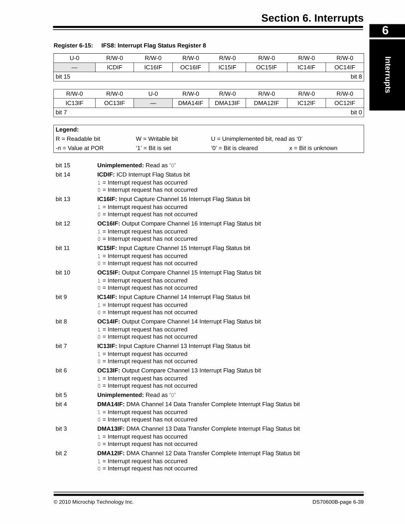
Register 6-15: IFS8: Interrupt Flag Status Register 8
U-0 R/W-0 R/W-0 R/W-0 R/W-0 R/W-0 R/W-0 R/W-0— ICDIF IC16IF OC16IF IC15IF OC15IF IC14IF OC14IF
bit 15 bit 8
R/W-0 R/W-0 U-0 R/W-0 R/W-0 R/W-0 R/W-0 R/W-0IC13IF OC13IF — DMA14IF DMA13IF DMA12IF IC12IF OC12IF
bit 7 bit 0
Legend:R = Readable bit W = Writable bit U = Unimplemented bit, read as ‘0’-n = Value at POR ‘1’ = Bit is set ‘0’ = Bit is cleared x = Bit is unknown
bit 15 Unimplemented: Read as ‘0’bit 14 ICDIF: ICD Interrupt Flag Status bit
1 = Interrupt request has occurred0 = Interrupt request has not occurred
bit 13 IC16IF: Input Capture Channel 16 Interrupt Flag Status bit1 = Interrupt request has occurred0 = Interrupt request has not occurred
bit 12 OC16IF: Output Compare Channel 16 Interrupt Flag Status bit1 = Interrupt request has occurred0 = Interrupt request has not occurred
bit 11 IC15IF: Input Capture Channel 15 Interrupt Flag Status bit1 = Interrupt request has occurred0 = Interrupt request has not occurred
bit 10 OC15IF: Output Compare Channel 15 Interrupt Flag Status bit1 = Interrupt request has occurred0 = Interrupt request has not occurred
bit 9 IC14IF: Input Capture Channel 14 Interrupt Flag Status bit1 = Interrupt request has occurred0 = Interrupt request has not occurred
bit 8 OC14IF: Output Compare Channel 14 Interrupt Flag Status bit1 = Interrupt request has occurred0 = Interrupt request has not occurred
bit 7 IC13IF: Input Capture Channel 13 Interrupt Flag Status bit1 = Interrupt request has occurred0 = Interrupt request has not occurred
bit 6 OC13IF: Output Compare Channel 13 Interrupt Flag Status bit1 = Interrupt request has occurred0 = Interrupt request has not occurred
bit 5 Unimplemented: Read as ‘0’bit 4 DMA14IF: DMA Channel 14 Data Transfer Complete Interrupt Flag Status bit
1 = Interrupt request has occurred0 = Interrupt request has not occurred
bit 3 DMA13IF: DMA Channel 13 Data Transfer Complete Interrupt Flag Status bit1 = Interrupt request has occurred0 = Interrupt request has not occurred
bit 2 DMA12IF: DMA Channel 12 Data Transfer Complete Interrupt Flag Status bit1 = Interrupt request has occurred0 = Interrupt request has not occurred
© 2010 Microchip Technology Inc. DS70600B-page 6-39

dsPIC33E/PIC24E Family Reference Manual
bit 1 IC12IF: Input Capture Channel 12 Interrupt Flag Status bit1 = Interrupt request has occurred0 = Interrupt request has not occurred
bit 0 OC12IF: Output Compare Channel 12 Interrupt Flag Status bit1 = Interrupt request has occurred0 = Interrupt request has not occurred
Register 6-15: IFS8: Interrupt Flag Status Register 8 (Continued)
DS70600B-page 6-40 © 2010 Microchip Technology Inc.

Section 6. InterruptsInterrupts
6
Register 6-16: IEC0: Interrupt Enable Control Register 0
R/W-0 R/W-0 R/W-0 R/W-0 R/W-0 R/W-0 R/W-0 R/W-0NVMIE DMA1IE AD1IE U1TXIE U1RXIE SPI1IE SPI1EIE T3IE
bit 15 bit 8
R/W-0 R/W-0 R/W-0 R/W-0 R/W-0 R/W-0 R/W-0 R/W-0T2IE OC2IE IC2IE DMA0IE T1IE OC1IE IC1IE INT0IE
bit 7 bit 0
Legend:R = Readable bit W = Writable bit U = Unimplemented bit, read as ‘0’-n = Value at POR ‘1’ = Bit is set ‘0’ = Bit is cleared x = Bit is unknown
bit 15 NVMIE: Non-Volatile Memory Interrupt Enable bit1 = Interrupt request enabled0 = Interrupt request not enabled
bit 14 DMA1IE: DMA Channel 1 Data Transfer Complete Interrupt Enable bit1 = Interrupt request enabled0 = Interrupt request not enabled
bit 13 AD1IE: ADC1 Conversion Complete Interrupt Enable bit1 = Interrupt request enabled0 = Interrupt request not enabled
bit 12 U1TXIE: UART1 Transmitter Interrupt Enable bit1 = Interrupt request enabled0 = Interrupt request not enabled
bit 11 U1RXIE: UART1 Receiver Interrupt Enable bit1 = Interrupt request enabled0 = Interrupt request not enabled
bit 10 SPI1IE: SPI1 Event Interrupt Enable bit1 = Interrupt request enabled0 = Interrupt request not enabled
bit 9 SPI1EIE: SPI1 Error Interrupt Enable bit1 = Interrupt request enabled0 = Interrupt request not enabled
bit 8 T3IE: Timer3 Interrupt Enable bit1 = Interrupt request enabled0 = Interrupt request not enabled
bit 7 T2IE: Timer2 Interrupt Enable bit1 = Interrupt request enabled0 = Interrupt request not enabled
bit 6 OC2IE: Output Compare Channel 2 Interrupt Enable bit1 = Interrupt request enabled0 = Interrupt request not enabled
bit 5 IC2IE: Input Capture Channel 2 Interrupt Enable bit1 = Interrupt request enabled0 = Interrupt request not enabled
bit 4 DMA0IE: DMA Channel 0 Data Transfer Complete Interrupt Enable bit1 = Interrupt request enabled0 = Interrupt request not enabled
© 2010 Microchip Technology Inc. DS70600B-page 6-41
dsPIC33E/PIC24E Family Reference Manual
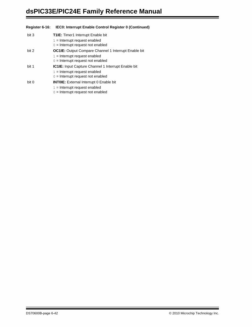
bit 3 T1IE: Timer1 Interrupt Enable bit1 = Interrupt request enabled0 = Interrupt request not enabled
bit 2 OC1IE: Output Compare Channel 1 Interrupt Enable bit1 = Interrupt request enabled0 = Interrupt request not enabled
bit 1 IC1IE: Input Capture Channel 1 Interrupt Enable bit1 = Interrupt request enabled0 = Interrupt request not enabled
bit 0 INT0IE: External Interrupt 0 Enable bit1 = Interrupt request enabled0 = Interrupt request not enabled
Register 6-16: IEC0: Interrupt Enable Control Register 0 (Continued)
DS70600B-page 6-42 © 2010 Microchip Technology Inc.

Section 6. InterruptsInterrupts
6
Register 6-17: IEC1: Interrupt Enable Control Register 1
R/W-0 R/W-0 R/W-0 R/W-0 R/W-0 R/W-0 R/W-0 R/W-0U2TXIE U2RXIE INT2IE T5IE T4IE OC4IE OC3IE DMA2IE
bit 15 bit 8
R/W-0 R/W-0 R/W-0 R/W-0 R/W-0 R/W-0 R/W-0 R/W-0IC8IE IC7IE AD2IE INT1IE CNIE CMIE MI2C1IE SI2C1IE
bit 7 bit 0
Legend:R = Readable bit W = Writable bit U = Unimplemented bit, read as ‘0’-n = Value at POR ‘1’ = Bit is set ‘0’ = Bit is cleared x = Bit is unknown
bit 15 U2TXIE: UART2 Transmitter Interrupt Enable bit1 = Interrupt request enabled0 = Interrupt request not enabled
bit 14 U2RXIE: UART2 Receiver Interrupt Enable bit1 = Interrupt request enabled0 = Interrupt request not enabled
bit 13 INT2IE: External Interrupt 2 Enable bit1 = Interrupt request enabled0 = Interrupt request not enabled
bit 12 T5IE: Timer5 Interrupt Enable bit1 = Interrupt request enabled0 = Interrupt request not enabled
bit 11 T4IE: Timer4 Interrupt Enable bit1 = Interrupt request enabled0 = Interrupt request not enabled
bit 10 OC4IE: Output Compare Channel 4 Interrupt Enable bit1 = Interrupt request enabled0 = Interrupt request not enabled
bit 9 OC3IE: Output Compare Channel 3 Interrupt Enable bit1 = Interrupt request enabled0 = Interrupt request not enabled
bit 8 DMA2IE: DMA Channel 2 Data Transfer Complete Interrupt Enable bit1 = Interrupt request enabled0 = Interrupt request not enabled
bit 7 IC8IE: Input Capture Channel 8 Interrupt Enable bit1 = Interrupt request enabled0 = Interrupt request not enabled
bit 6 IC7IE: Input Capture Channel 7 Interrupt Enable bit1 = Interrupt request enabled0 = Interrupt request not enabled
bit 5 AD2IE: ADC2 Conversion Complete Interrupt Enable bit1 = Interrupt request enabled0 = Interrupt request not enabled
bit 4 INT1IE: External Interrupt 1 Enable bit1 = Interrupt request enabled0 = Interrupt request not enabled
© 2010 Microchip Technology Inc. DS70600B-page 6-43

dsPIC33E/PIC24E Family Reference Manual
bit 3 CNIE: Input Change Notification Interrupt Enable bit1 = Interrupt request enabled0 = Interrupt request not enabled
bit 2 CMIE: Comparator Interrupt Enable bit1 = Interrupt request enabled0 = Interrupt request not enabled
bit 1 MI2C1IE: I2C1 Master Events Interrupt Enable bit1 = Interrupt request enabled0 = Interrupt request not enabled
bit 0 SI2C1IE: I2C1 Slave Events Interrupt Enable bit1 = Interrupt request enabled0 = Interrupt request not enabled
Register 6-17: IEC1: Interrupt Enable Control Register 1 (Continued)
DS70600B-page 6-44 © 2010 Microchip Technology Inc.

Section 6. InterruptsInterrupts
6
Register 6-18: IEC2: Interrupt Enable Control Register 2
R/W-0 R/W-0 R/W-0 R/W-0 R/W-0 R/W-0 R/W-0 R/W-0T6IE DMA4IE PMPIE OC8IE OC7IE OC6IE OC5IE IC6IE
bit 15 bit 8
R/W-0 R/W-0 R/W-0 R/W-0 R/W-0 R/W-0 R/W-0 R/W-0IC5IE IC4IE IC3IE DMA3IE C1IE C1RXIE SPI2IE SPI2EIE
bit 7 bit 0
Legend:R = Readable bit W = Writable bit U = Unimplemented bit, read as ‘0’-n = Value at POR ‘1’ = Bit is set ‘0’ = Bit is cleared x = Bit is unknown
bit 15 T6IE: Timer6 Interrupt Enable bit1 = Interrupt request enabled0 = Interrupt request not enabled
bit 14 DMA4IE: DMA Channel 4 Data Transfer Complete Interrupt Enable bit1 = Interrupt request enabled0 = Interrupt request not enabled
bit 13 PMPIE: Parallel Master Port Interrupt Enable bit1 = Interrupt request enabled0 = Interrupt request not enabled
bit 12 OC8IE: Output Compare Channel 8 Interrupt Enable bit1 = Interrupt request enabled0 = Interrupt request not enabled
bit 11 OC7IE: Output Compare Channel 7 Interrupt Enable bit1 = Interrupt request enabled0 = Interrupt request not enabled
bit 10 OC6IE: Output Compare Channel 6 Interrupt Enable bit1 = Interrupt request enabled0 = Interrupt request not enabled
bit 9 OC5IE: Output Compare Channel 5 Interrupt Enable bit1 = Interrupt request enabled0 = Interrupt request not enabled
bit 8 IC6IE: Input Capture Channel 6 Interrupt Enable bit1 = Interrupt request enabled0 = Interrupt request not enabled
bit 7 IC5IE: Input Capture Channel 5 Interrupt Enable bit1 = Interrupt request enabled0 = Interrupt request not enabled
bit 6 IC4IE: Input Capture Channel 4 Interrupt Enable bit1 = Interrupt request enabled0 = Interrupt request not enabled
bit 5 IC3IE: Input Capture Channel 3 Interrupt Enable bit1 = Interrupt request enabled0 = Interrupt request not enabled
bit 4 DMA3IE: DMA Channel 3 Data Transfer Complete Interrupt Enable bit1 = Interrupt request enabled0 = Interrupt request not enabled
© 2010 Microchip Technology Inc. DS70600B-page 6-45

dsPIC33E/PIC24E Family Reference Manual
bit 3 C1IE: ECAN1 Event Interrupt Enable bit1 = Interrupt request enabled0 = Interrupt request not enabled
bit 2 C1RXIE: ECAN1 Receive Data Ready Interrupt Enable bit1 = Interrupt request enabled0 = Interrupt request not enabled
bit 1 SPI2IE: SPI2 Event Interrupt Enable bit1 = Interrupt request enabled0 = Interrupt request not enabled
bit 0 SPI2EIE: SPI2 Error Interrupt Enable bit1 = Interrupt request enabled0 = Interrupt request not enabled
Register 6-18: IEC2: Interrupt Enable Control Register 2 (Continued)
DS70600B-page 6-46 © 2010 Microchip Technology Inc.

Section 6. InterruptsInterrupts
6
Register 6-19: IEC3: Interrupt Enable Control Register 3
U-0 R/W-0 R/W-0 R/W-0 R/W-0 R/W-0 R/W-0 R/W-0— RTCIE DMA5IE DCIIE DCIEIE QEI1IE PSEMIE C2IE
bit 15 bit 8
R/W-0 R/W-0 R/W-0 R/W-0 R/W-0 R/W-0 R/W-0 R/W-0C2RXIE INT4IE INT3IE T9IE T8IE MI2C2IE SI2C2IE T7IE
bit 7 bit 0
Legend:R = Readable bit W = Writable bit U = Unimplemented bit, read as ‘0’-n = Value at POR ‘1’ = Bit is set ‘0’ = Bit is cleared x = Bit is unknown
bit 15 Unimplemented: Read as ‘0’bit 14 RTCIE: Real-Time Clock and Calender Interrupt Enable bit
1 = Interrupt request enabled 0 = Interrupt request not enabled
bit 13 DMA5IE: DMA Channel 5 Data Transfer Complete Interrupt Enable bit1 = Interrupt request enabled0 = Interrupt request not enabled
bit 12 DCIIE: DCI Event Interrupt Enable bit1 = Interrupt request enabled0 = Interrupt request not enabled
bit 11 DCIEIE: DCI Error Interrupt Enable bit1 = Interrupt request enabled0 = Interrupt request not enabled
bit 10 QEI1IE: QEI1 Event Interrupt Enable bit1 = Interrupt request enabled0 = Interrupt request not enabled
bit 9 PSEMIE: PWM Primary Event Interrupt Enable bit1 = Interrupt request enabled0 = Interrupt request not enabled
bit 8 C2IE: ECAN2 Event Interrupt Enable bit1 = Interrupt request enabled0 = Interrupt request not enabled
bit 7 C2RXIE: ECAN2 Receive Data Ready Interrupt Enable bit1 = Interrupt request enabled0 = Interrupt request not enabled
bit 6 INT4IE: External Interrupt 4 Enable bit1 = Interrupt request enabled0 = Interrupt request not enabled
bit 5 INT3IE: External Interrupt 3 Enable bit1 = Interrupt request enabled0 = Interrupt request not enabled
bit 4 T9IE: Timer9 Interrupt Enable bit1 = Interrupt request enabled0 = Interrupt request not enabled
bit 3 T8IE: Timer8 Interrupt Enable bit1 = Interrupt request enabled0 = Interrupt request not enabled
© 2010 Microchip Technology Inc. DS70600B-page 6-47

dsPIC33E/PIC24E Family Reference Manual
bit 2 MI2C2IE: I2C2 Master Events Interrupt Enable bit1 = Interrupt request enabled0 = Interrupt request not enabled
bit 1 SI2C2IE: I2C2 Slave Events Interrupt Enable bit1 = Interrupt request enabled0 = Interrupt request not enabled
bit 0 T7IE: Timer7 Interrupt Enable bit1 = Interrupt request enabled0 = Interrupt request not enabled
Register 6-19: IEC3: Interrupt Enable Control Register 3 (Continued)
DS70600B-page 6-48 © 2010 Microchip Technology Inc.

Section 6. InterruptsInterrupts
6
Register 6-20: IEC4: Interrupt Enable Control Register 4
U-0 U-0 U-0 U-0 R/W-0 U-0 R/W-0 U-0— — — — QEI2IE — PSESMIE —
bit 15 bit 8
R/W-0 R/W-0 R/W-0 R/W-0 R/W-0 R/W-0 R/W-0 U-0C2TXIE C1TXIE DMA7IE DMA6IE CRCIE U2EIE U1EIE —
bit 7 bit 0
Legend:R = Readable bit W = Writable bit U = Unimplemented bit, read as ‘0’-n = Value at POR ‘1’ = Bit is set ‘0’ = Bit is cleared x = Bit is unknown
bit 15-12 Unimplemented: Read as ‘0’bit 11 QEI2IE: QEI2 Interrupt Enable bit
1 = Interrupt request enabled0 = Interrupt request not enabled
bit 10 Unimplemented: Read as ‘0’bit 9 PSESMIE: PWM Secondary Special Event Match Interrupt Enable bit
1 = Interrupt request enabled0 = Interrupt request not enabled
bit 8 Unimplemented: Read as ‘0’bit 7 C2TXIE: ECAN2 Transmit Data Request Interrupt Enable bit
1 = Interrupt request enabled0 = Interrupt request not enabled
bit 6 C1TXIE: ECAN1 Transmit Data Request Interrupt Enable bit1 = Interrupt request enabled0 = Interrupt request not enabled
bit 5 DMA7IE: DMA Channel 7 Data Transfer Complete Enable Status bit1 = Interrupt request enabled0 = Interrupt request not enabled
bit 4 DMA6IE: DMA Channel 6 Data Transfer Complete Enable Status bit1 = Interrupt request enabled0 = Interrupt request not enabled
bit 3 CRCIE: CRC Interrupt Enable bit1 = Interrupt request enabled0 = Interrupt request not enabled
bit 2 U2EIE: UART2 Error Interrupt Enable bit1 = Interrupt request enabled0 = Interrupt request not enabled
bit 1 U1EIE: UART1 Error Interrupt Enable bit1 = Interrupt request enabled0 = Interrupt request not enabled
bit 0 Unimplemented: Read as ‘0’
© 2010 Microchip Technology Inc. DS70600B-page 6-49

dsPIC33E/PIC24E Family Reference Manual
Register 6-21: IEC5: Interrupt Enable Control Register 5
R/W-0 R/W-0 R/W-0 R/W-0 R/W-0 R/W-0 R/W-0 R/W-0PWM2IE PWM1IE IC9IE OC9IE SPI3IE SPI3EIE U4TXIE U4RXIE
bit 15 bit 8
R/W-0 R/W-0 U-0 U-0 R/W-0 R/W-0 R/W-0 U-0U4EIE USBIE — — U3TXIE U3RXIE U3EIE —
bit 7 bit 0
Legend:R = Readable bit W = Writable bit U = Unimplemented bit, read as ‘0’-n = Value at POR ‘1’ = Bit is set ‘0’ = Bit is cleared x = Bit is unknown
bit 15 PWM2IE: PWM Generator 2 Interrupt Enable bit1 = Interrupt request enabled0 = Interrupt request not enabled
bit 14 PWM1IE: PWM Generator 1 Interrupt Enable bit1 = Interrupt request enabled0 = Interrupt request not enabled
bit 13 IC9IE: Input Capture Channel 9 Interrupt Enable bit1 = Interrupt request enabled0 = Interrupt request not enabled
bit 12 OC9IE: Output Compare Channel 9 Interrupt Enable bit1 = Interrupt request enabled0 = Interrupt request not enabled
bit 11 SPI3IE: SPI3 Interrupt Enable bit1 = Interrupt request enabled0 = Interrupt request not enabled
bit 10 SPI3EIE: SPI3 Error Interrupt Enables bit1 = Interrupt request enabled0 = Interrupt request not enabled
bit 9 U4TXIE: UART4 TX Interrupt Enable bit 1 = Interrupt request enabled0 = Interrupt request not enabled
bit 8 U4RXIE: UART4 RX Interrupt Enable bit 1 = Interrupt request enabled0 = Interrupt request not enabled
bit 7 U4EIE: UART4 Error Interrupt Enable bit1 = Interrupt request enabled0 = Interrupt request not enabled
bit 6 USBIE: USB Interrupt Enable bit 1 = Interrupt request enabled0 = Interrupt request not enabled
bit 5-4 Unimplemented: Read as ‘0’bit 3 U3TXIE: UART3 TX Interrupt Enable bit
1 = Interrupt request enabled0 = Interrupt request not enabled
bit 2 U3RXIE: UART3 RX Interrupt Enable bit1 = Interrupt request enabled0 = Interrupt request not enabled
DS70600B-page 6-50 © 2010 Microchip Technology Inc.

Section 6. InterruptsInterrupts
6
bit 1 U3EIE: UART3 Error Interrupt Enable bit1 = Interrupt request enabled0 = Interrupt request not enabled
bit 0 Unimplemented: Read as ‘0’
Register 6-21: IEC5: Interrupt Enable Control Register 5 (Continued)
© 2010 Microchip Technology Inc. DS70600B-page 6-51

dsPIC33E/PIC24E Family Reference Manual
Register 6-22: IEC6: Interrupt Enable Control Register 6
U-0 U-0 U-0 U-0 U-0 U-0 U-0 U-0— — — — — — — —
bit 15 bit 8
U-0 U-0 U-0 R/W-0 R/W-0 R/W-0 R/W-0 R/W-0— — — PWM7IE PWM6IE PWM5IE PWM4IE PWM3IE
bit 7 bit 0
Legend:R = Readable bit W = Writable bit U = Unimplemented bit, read as ‘0’-n = Value at POR ‘1’ = Bit is set ‘0’ = Bit is cleared x = Bit is unknown
bit 15-5 Unimplemented: Read as ‘0’bit 4 PWM7IE: PWM Generator 7 Interrupt Enable bit
1 = Interrupt request enabled0 = Interrupt request not enabled
bit 3 PWM6IE: PWM Generator 6 Interrupt Enable bit1 = Interrupt request enabled0 = Interrupt request not enabled
bit 2 PWM5IE: PWM Generator 5 Interrupt Enable bit1 = Interrupt request enabled0 = Interrupt request not enabled
bit 1 PWM4IE: PWM Generator 4 Interrupt Enable bit1 = Interrupt request enabled0 = Interrupt request not enabled
bit 0 PWM3IE: PWM Generator 3 Interrupt Enable bit1 = Interrupt request enabled0 = Interrupt request not enabled
DS70600B-page 6-52 © 2010 Microchip Technology Inc.

Section 6. InterruptsInterrupts
6
Register 6-23: IEC7: Interrupt Enable Control Register 7
R/W-0 R/W-0 R/W-0 R/W-0 R/W-0 R/W-0 R/W-0 R/W-0IC11IE OC11IE IC10IE OC10IE SPI4IE SPI4EIE DMA11IE DMA10IE
bit 15 bit 8
R/W-0 R/W-0 U-0 U-0 U-0 U-0 U-0 U-0DMA9IE DMA8IE — — — — — —
bit 7 bit 0
Legend:R = Readable bit W = Writable bit U = Unimplemented bit, read as ‘0’-n = Value at POR ‘1’ = Bit is set ‘0’ = Bit is cleared x = Bit is unknown
bit 15 IC11IE: Input Capture Channel 11 Interrupt Enable bit1 = Interrupt request has occurred0 = Interrupt request has not occurred
bit 14 OC11IE: Output Compare Channel 11 Interrupt Enable bit1 = Interrupt request has occurred0 = Interrupt request has not occurred
bit 13 IC10IE: Input Capture Channel 10 Interrupt Enable bit1 = Interrupt request has occurred0 = Interrupt request has not occurred
bit 12 OC10IE: Output Compare Channel 10 Interrupt Enable bit1 = Interrupt request has occurred0 = Interrupt request has not occurred
bit 11 SPI4IE: SPI4 Interrupt Enable bit1 = Interrupt request has occurred0 = Interrupt request has not occurred
bit 10 SPI4EIE: SPI4 Error Interrupt Enable bit1 = Interrupt request has occurred0 = Interrupt request has not occurred
bit 9 DMA11IE: DMA Channel 11 Data Transfer Complete Interrupt Enable bit1 = Interrupt request has occurred0 = Interrupt request has not occurred
bit 8 DMA10IE: DMA Channel 10 Data Transfer Complete Interrupt Enable bit1 = Interrupt request has occurred0 = Interrupt request has not occurred
bit 7 DMA9IE: DMA Channel 9 Data Transfer Complete Interrupt Enable bit1 = Interrupt request has occurred0 = Interrupt request has not occurred
bit 6 DMA8IE: DMA Channel 8 Data Transfer Complete Interrupt Enable bit1 = Interrupt request has occurred0 = Interrupt request has not occurred
bit 5-0 Unimplemented: Read as ‘0’
© 2010 Microchip Technology Inc. DS70600B-page 6-53

dsPIC33E/PIC24E Family Reference Manual
Register 6-24: IEC8: Interrupt Enable Control Register 8
U-0 R/W-0 R/W-0 R/W-0 R/W-0 R/W-0 R/W-0 R/W-0— ICDIE IC16IE OC16IE IC15IE OC15IE IC14IE OC14IE
bit 15 bit 8
R/W-0 R/W-0 U-0 R/W-0 R/W-0 R/W-0 R/W-0 R/W-0IC13IE OC13IE — DMA14IE DMA13IE DMA12IE IC12IE OC12IE
bit 7 bit 0
Legend:R = Readable bit W = Writable bit U = Unimplemented bit, read as ‘0’-n = Value at POR ‘1’ = Bit is set ‘0’ = Bit is cleared x = Bit is unknown
bit 15 Unimplemented: Read as ‘0’bit 14 ICDIE: ICD Interrupt Enable bit
1 = Interrupt request enabled0 = Interrupt request not enabled
bit 13 IC16IE: Input Capture Channel 16 Interrupt Enable bit1 = Interrupt request enabled0 = Interrupt request not enabled
bit 12 OC16IE: Output Compare Channel 16 Interrupt Enable bit1 = Interrupt request enabled0 = Interrupt request not enabled
bit 11 IC15IE: Input Capture Channel 15 Interrupt Enable bit1 = Interrupt request enabled0 = Interrupt request not enabled
bit 10 OC15IE: Output Compare Channel 15 Interrupt Enable bit1 = Interrupt request enabled0 = Interrupt request not enabled
bit 9 IC14IE: Input Capture Channel 14 Interrupt Enable bit1 = Interrupt request enabled0 = Interrupt request not enabled
bit 8 OC14IE: Output Compare Channel 14 Interrupt Enable bit1 = Interrupt request enabled0 = Interrupt request not enabled
bit 7 IC13IE: Input Capture Channel 13 Interrupt Enable bit1 = Interrupt request enabled0 = Interrupt request not enabled
bit 6 OC13IE: Output Compare 13 Interrupt Enable bit1 = Interrupt request enabled0 = Interrupt request not enabled
bit 5 Unimplemented: Read as ‘0’bit 4 DMA14IE: DMA Channel 14 Data Transfer Complete Interrupt Enable bit
1 = Interrupt request enabled0 = Interrupt request not enabled
bit 3 DMA13IE: DMA Channel 13 Data Transfer Complete Interrupt Enable bit1 = Interrupt request enabled0 = Interrupt request not enabled
bit 2 DMA12IE: DMA Channel 12 Data Transfer Complete Interrupt Enable bit1 = Interrupt request enabled0 = Interrupt request not enabled
DS70600B-page 6-54 © 2010 Microchip Technology Inc.

Section 6. InterruptsInterrupts
6
bit 1 IC12IE: Input Capture Channel 12 Interrupt Enable bit1 = Interrupt request enabled0 = Interrupt request not enabled
bit 0 OC12IE: Output Compare Channel 12 Interrupt Enable bit1 = Interrupt request enabled0 = Interrupt request not enabled
Register 6-24: IEC8: Interrupt Enable Control Register 8 (Continued)
© 2010 Microchip Technology Inc. DS70600B-page 6-55
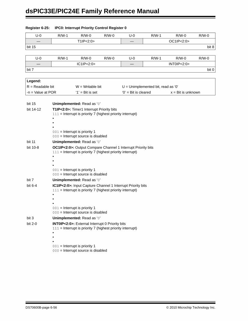
dsPIC33E/PIC24E Family Reference Manual
Register 6-25: IPC0: Interrupt Priority Control Register 0
U-0 R/W-1 R/W-0 R/W-0 U-0 R/W-1 R/W-0 R/W-0— T1IP<2:0> — OC1IP<2:0>
bit 15 bit 8
U-0 R/W-1 R/W-0 R/W-0 U-0 R/W-1 R/W-0 R/W-0— IC1IP<2:0> — INT0IP<2:0>
bit 7 bit 0
Legend:R = Readable bit W = Writable bit U = Unimplemented bit, read as ‘0’-n = Value at POR ‘1’ = Bit is set ‘0’ = Bit is cleared x = Bit is unknown
bit 15 Unimplemented: Read as ‘0’bit 14-12 T1IP<2:0>: Timer1 Interrupt Priority bits
111 = Interrupt is priority 7 (highest priority interrupt)•••001 = Interrupt is priority 1000 = Interrupt source is disabled
bit 11 Unimplemented: Read as ‘0’bit 10-8 OC1IP<2:0>: Output Compare Channel 1 Interrupt Priority bits
111 = Interrupt is priority 7 (highest priority interrupt)•••001 = Interrupt is priority 1000 = Interrupt source is disabled
bit 7 Unimplemented: Read as ‘0’bit 6-4 IC1IP<2:0>: Input Capture Channel 1 Interrupt Priority bits
111 = Interrupt is priority 7 (highest priority interrupt)•••001 = Interrupt is priority 1000 = Interrupt source is disabled
bit 3 Unimplemented: Read as ‘0’bit 2-0 INT0IP<2:0>: External Interrupt 0 Priority bits
111 = Interrupt is priority 7 (highest priority interrupt)•••001 = Interrupt is priority 1000 = Interrupt source is disabled
DS70600B-page 6-56 © 2010 Microchip Technology Inc.

Section 6. InterruptsInterrupts
6
Register 6-26: IPC1: Interrupt Priority Control Register 1
U-0 R/W-1 R/W-0 R/W-0 U-0 R/W-1 R/W-0 R/W-0— T2IP<2:0> — OC2IP<2:0>
bit 15 bit 8
U-0 R/W-1 R/W-0 R/W-0 U-0 R/W-1 R/W-0 R/W-0— IC2IP<2:0> — DMA0IP<2:0>
bit 7 bit 0
Legend:R = Readable bit W = Writable bit U = Unimplemented bit, read as ‘0’-n = Value at POR ‘1’ = Bit is set ‘0’ = Bit is cleared x = Bit is unknown
bit 15 Unimplemented: Read as ‘0’bit 14-12 T2IP<2:0>: Timer2 Interrupt Priority bits
111 = Interrupt is priority 7 (highest priority interrupt)•••001 = Interrupt is priority 1000 = Interrupt source is disabled
bit 11 Unimplemented: Read as ‘0’bit 10-8 OC2IP<2:0>: Output Compare Channel 2 Interrupt Priority bits
111 = Interrupt is priority 7 (highest priority interrupt)•••001 = Interrupt is priority 1000 = Interrupt source is disabled
bit 7 Unimplemented: Read as ‘0’bit 6-4 IC2IP<2:0>: Input Capture Channel 2 Interrupt Priority bits
111 = Interrupt is priority 7 (highest priority interrupt)•••001 = Interrupt is priority 1000 = Interrupt source is disabled
bit 3 Unimplemented: Read as ‘0’bit 2-0 DMA0IP<2:0>: DMA Channel 0 Data Transfer Complete Interrupt Priority bits
111 = Interrupt is priority 7 (highest priority interrupt)•••001 = Interrupt is priority 1000 = Interrupt source is disabled
© 2010 Microchip Technology Inc. DS70600B-page 6-57

dsPIC33E/PIC24E Family Reference Manual
Register 6-27: IPC2: Interrupt Priority Control Register 2
U-0 R/W-1 R/W-0 R/W-0 U-0 R/W-1 R/W-0 R/W-0— U1RXIP<2:0> — SPI1IP<2:0>
bit 15 bit 8
U-0 R/W-1 R/W-0 R/W-0 U-0 R/W-1 R/W-0 R/W-0— SPI1EIP<2:0> — T3IP<2:0>
bit 7 bit 0
Legend:R = Readable bit W = Writable bit U = Unimplemented bit, read as ‘0’-n = Value at POR ‘1’ = Bit is set ‘0’ = Bit is cleared x = Bit is unknown
bit 15 Unimplemented: Read as ‘0’bit 14-12 U1RXIP<2:0>: UART1 Receiver Interrupt Priority bits
111 = Interrupt is priority 7 (highest priority interrupt)•••001 = Interrupt is priority 1000 = Interrupt source is disabled
bit 11 Unimplemented: Read as ‘0’bit 10-8 SPI1IP<2:0>: SPI1 Event Interrupt Priority bits
111 = Interrupt is priority 7 (highest priority interrupt)•••001 = Interrupt is priority 1000 = Interrupt source is disabled
bit 7 Unimplemented: Read as ‘0’bit 6-4 SPI1EIP<2:0>: SPI1 Error Interrupt Priority bits
111 = Interrupt is priority 7 (highest priority interrupt)•••001 = Interrupt is priority 1000 = Interrupt source is disabled
bit 3 Unimplemented: Read as ‘0’bit 2-0 T3IP<2:0>: Timer3 Interrupt Priority bits
111 = Interrupt is priority 7 (highest priority interrupt)•••001 = Interrupt is priority 1000 = Interrupt source is disabled
DS70600B-page 6-58 © 2010 Microchip Technology Inc.

Section 6. InterruptsInterrupts
6
Register 6-28: IPC3: Interrupt Priority Control Register 3U-0 R/W-1 R/W-0 R/W-0 U-0 R/W-1 R/W-0 R/W-0— NVMIP<2:0> — DMA1IP<2:0>
bit 15 bit 8
U-0 R/W-1 R/W-0 R/W-0 U-0 R/W-1 R/W-0 R/W-0— AD1IP<2:0> — U1TXIP<2:0>
bit 7 bit 0
Legend:R = Readable bit W = Writable bit U = Unimplemented bit, read as ‘0’-n = Value at POR ‘1’ = Bit is set ‘0’ = Bit is cleared x = Bit is unknown
bit 15 Unimplemented: Read as ‘0’bit 14-12 NVMIP<2:0>: Non-Volatile Memory Interrupt Priority bits
111 = Interrupt is priority 7 (highest priority interrupt)•••001 = Interrupt is priority 1000 = Interrupt source is disabled
bit 11 Unimplemented: Read as ‘0’bit 10-8 DMA1IP<2:0>: DMA Channel 1 Data Transfer Complete Interrupt Priority bits
111 = Interrupt is priority 7 (highest priority interrupt)•••001 = Interrupt is priority 1000 = Interrupt source is disabled
bit 7 Unimplemented: Read as ‘0’bit 6-4 AD1IP<2:0>: ADC1 Conversion Complete Interrupt Priority bits
111 = Interrupt is priority 7 (highest priority interrupt)•••001 = Interrupt is priority 1000 = Interrupt source is disabled
bit 3 Unimplemented: Read as ‘0’bit 2-0 U1TXIP<2:0>: UART1 Transmitter Interrupt Priority bits
111 = Interrupt is priority 7 (highest priority interrupt)•••001 = Interrupt is priority 1000 = Interrupt source is disabled
© 2010 Microchip Technology Inc. DS70600B-page 6-59

dsPIC33E/PIC24E Family Reference Manual
Register 6-29: IPC4: Interrupt Priority Control Register 4
U-0 R/W-1 R/W-0 R/W-0 U-0 R/W-1 R/W-0 R/W-0— CNIP<2:0> — CMIP<2:0>
bit 15 bit 8
U-0 R/W-1 R/W-0 R/W-0 U-0 R/W-1 R/W-0 R/W-0— MI2C1IP<2:0> — SI2C1IP<2:0>
bit 7 bit 0
Legend:R = Readable bit W = Writable bit U = Unimplemented bit, read as ‘0’-n = Value at POR ‘1’ = Bit is set ‘0’ = Bit is cleared x = Bit is unknown
bit 15 Unimplemented: Read as ‘0’bit 14-12 CNIP<2:0>: Change Notification Interrupt Priority bits
111 = Interrupt is priority 7 (highest priority interrupt)•••001 = Interrupt is priority 1000 = Interrupt source is disabled
bit 11 Unimplemented: Read as ‘0’bit 10-8 CMIP<2:0>: Comparator Interrupt Priority bits
111 = Interrupt is priority 7 (highest priority interrupt)•••001 = Interrupt is priority 1000 = Interrupt source is disabled
bit 7 Unimplemented: Read as ‘0’bit 6-4 MI2C1IP<2:0>: I2C1 Master Events Interrupt Priority bits
111 = Interrupt is priority 7 (highest priority interrupt)•••001 = Interrupt is priority 1000 = Interrupt source is disabled
bit 3 Unimplemented: Read as ‘0’bit 2-0 SI2C1IP<2:0>: I2C1 Slave Events Interrupt Priority bits
111 = Interrupt is priority 7 (highest priority interrupt)•••001 = Interrupt is priority 1000 = Interrupt source is disabled
DS70600B-page 6-60 © 2010 Microchip Technology Inc.

Section 6. InterruptsInterrupts
6
Register 6-30: IPC5: Interrupt Priority Control Register 5U-0 R/W-1 R/W-0 R/W-0 U-0 R/W-1 R/W-0 R/W-0— IC8IP<2:0> — IC7IP<2:0>
bit 15 bit 8
U-0 R/W-1 R/W-0 R/W-0 U-0 R/W-1 R/W-0 R/W-0— AD2IP<2:0> — INT1IP<2:0>
bit 7 bit 0
Legend:R = Readable bit W = Writable bit U = Unimplemented bit, read as ‘0’-n = Value at POR ‘1’ = Bit is set ‘0’ = Bit is cleared x = Bit is unknown
bit 15 Unimplemented: Read as ‘0’bit 14-12 IC8IP<2:0>: Input Capture Channel 8 Interrupt Priority bits
111 = Interrupt is priority 7 (highest priority interrupt)•••001 = Interrupt is priority 1000 = Interrupt source is disabled
bit 11 Unimplemented: Read as ‘0’bit 10-8 IC7IP<2:0>: Input Capture Channel 7 Interrupt Priority bits
111 = Interrupt is priority 7 (highest priority interrupt)•••001 = Interrupt is priority 1000 = Interrupt source is disabled
bit 7 Unimplemented: Read as ‘0’bit 6-4 AD2IP<2:0>: ADC2 Conversion Complete Interrupt Priority bits
111 = Interrupt is priority 7 (highest priority interrupt)•••001 = Interrupt is priority 1000 = Interrupt source is disabled
bit 3 Unimplemented: Read as ‘0’bit 2-0 INT1IP<2:0>: External Interrupt 1 Priority bits
111 = Interrupt is priority 7 (highest priority interrupt)•••001 = Interrupt is priority 1000 = Interrupt source is disabled
© 2010 Microchip Technology Inc. DS70600B-page 6-61

dsPIC33E/PIC24E Family Reference Manual
Register 6-31: IPC6: Interrupt Priority Control Register 6
U-0 R/W-1 R/W-0 R/W-0 U-0 R/W-1 R/W-0 R/W-0— T4IP<2:0> — OC4IP<2:0>
bit 15 bit 8
U-0 R/W-1 R/W-0 R/W-0 U-0 R/W-1 R/W-0 R/W-0— OC3IP<2:0> — DMA2IP<2:0>
bit 7 bit 0
Legend:R = Readable bit W = Writable bit U = Unimplemented bit, read as ‘0’-n = Value at POR ‘1’ = Bit is set ‘0’ = Bit is cleared x = Bit is unknown
bit 15 Unimplemented: Read as ‘0’bit 14-12 T4IP<2:0>: Timer4 Interrupt Priority bits
111 = Interrupt is priority 7 (highest priority interrupt)•••001 = Interrupt is priority 1000 = Interrupt source is disabled
bit 11 Unimplemented: Read as ‘0’bit 10-8 OC4IP<2:0>: Output Compare Channel 4 Interrupt Priority bits
111 = Interrupt is priority 7 (highest priority interrupt)•••001 = Interrupt is priority 1000 = Interrupt source is disabled
bit 7 Unimplemented: Read as ‘0’bit 6-4 OC3IP<2:0>: Output Compare Channel 3 Interrupt Priority bits
111 = Interrupt is priority 7 (highest priority interrupt)•••001 = Interrupt is priority 1000 = Interrupt source is disabled
bit 3 Unimplemented: Read as ‘0’bit 2-0 DMA2IP<2:0>: DMA Channel 2 Data Transfer Complete Interrupt Priority bits
111 = Interrupt is priority 7 (highest priority interrupt)•••001 = Interrupt is priority 1000 = Interrupt source is disabled
DS70600B-page 6-62 © 2010 Microchip Technology Inc.

Section 6. InterruptsInterrupts
6
Register 6-32: IPC7: Interrupt Priority Control Register 7U-0 R/W-1 R/W-0 R/W-0 U-0 R/W-1 R/W-0 R/W-0— U2TXIP<2:0> — U2RXIP<2:0>
bit 15 bit 8
U-0 R/W-1 R/W-0 R/W-0 U-0 R/W-1 R/W-0 R/W-0— INT2IP<2:0> — T5IP<2:0>
bit 7 bit 0
Legend:R = Readable bit W = Writable bit U = Unimplemented bit, read as ‘0’-n = Value at POR ‘1’ = Bit is set ‘0’ = Bit is cleared x = Bit is unknown
bit 15 Unimplemented: Read as ‘0’bit 14-12 U2TXIP<2:0>: UART2 Transmitter Interrupt Priority bits
111 = Interrupt is priority 7 (highest priority interrupt)•••001 = Interrupt is priority 1000 = Interrupt source is disabled
bit 11 Unimplemented: Read as ‘0’bit 10-8 U2RXIP<2:0>: UART2 Receiver Interrupt Priority bits
111 = Interrupt is priority 7 (highest priority interrupt)•••001 = Interrupt is priority 1000 = Interrupt source is disabled
bit 7 Unimplemented: Read as ‘0’bit 6-4 INT2IP<2:0>: External Interrupt 2 Priority bits
111 = Interrupt is priority 7 (highest priority interrupt)•••001 = Interrupt is priority 1000 = Interrupt source is disabled
bit 3 Unimplemented: Read as ‘0’bit 2-0 T5IP<2:0>: Timer5 Interrupt Priority bits
111 = Interrupt is priority 7 (highest priority interrupt)•••001 = Interrupt is priority 1000 = Interrupt source is disabled
© 2010 Microchip Technology Inc. DS70600B-page 6-63

dsPIC33E/PIC24E Family Reference Manual
Register 6-33: IPC8: Interrupt Priority Control Register 8
U-0 R/W-1 R/W-0 R/W-0 U-0 R/W-1 R/W-0 R/W-0— C1IP<2:0> — C1RXIP<2:0>
bit 15 bit 8
U-0 R/W-1 R/W-0 R/W-0 U-0 R/W-1 R/W-0 R/W-0— SPI2IP<2:0> — SPI2EIP<2:0>
bit 7 bit 0
Legend:R = Readable bit W = Writable bit U = Unimplemented bit, read as ‘0’-n = Value at POR ‘1’ = Bit is set ‘0’ = Bit is cleared x = Bit is unknown
bit 15 Unimplemented: Read as ‘0’bit 14-12 C1IP<2:0>: ECAN1 Event Interrupt Priority bits
111 = Interrupt is priority 7 (highest priority interrupt)•••001 = Interrupt is priority 1000 = Interrupt source is disabled
bit 11 Unimplemented: Read as ‘0’bit 10-8 C1RXIP<2:0>: ECAN1 Receive Data Ready Interrupt Priority bits
111 = Interrupt is priority 7 (highest priority interrupt)•••001 = Interrupt is priority 1000 = Interrupt source is disabled
bit 7 Unimplemented: Read as ‘0’bit 6-4 SPI2IP<2:0>: SPI2 Event Interrupt Priority bits
111 = Interrupt is priority 7 (highest priority interrupt)•••001 = Interrupt is priority 1000 = Interrupt source is disabled
bit 3 Unimplemented: Read as ‘0’bit 2-0 SPI2EIP<2:0>: SPI2 Error Interrupt Priority bits
111 = Interrupt is priority 7 (highest priority interrupt)•••001 = Interrupt is priority 1000 = Interrupt source is disabled
DS70600B-page 6-64 © 2010 Microchip Technology Inc.

Section 6. InterruptsInterrupts
6
Register 6-34: IPC9: Interrupt Priority Control Register 9U-0 R/W-1 R/W-0 R/W-0 U-0 R/W-1 R/W-0 R/W-0— IC5IP<2:0> — IC4IP<2:0>
bit 15 bit 8
U-0 R/W-1 R/W-0 R/W-0 U-0 R/W-1 R/W-0 R/W-0— IC3IP<2:0> — DMA3IP<2:0>
bit 7 bit 0
Legend:R = Readable bit W = Writable bit U = Unimplemented bit, read as ‘0’-n = Value at POR ‘1’ = Bit is set ‘0’ = Bit is cleared x = Bit is unknown
bit 15 Unimplemented: Read as ‘0’bit 14-12 IC5IP<2:0>: Input Capture Channel 5 Interrupt Priority bits
111 = Interrupt is priority 7 (highest priority interrupt)•••001 = Interrupt is priority 1000 = Interrupt source is disabled
bit 11 Unimplemented: Read as ‘0’bit 10-8 IC4IP<2:0>: Input Capture Channel 4 Interrupt Priority bits
111 = Interrupt is priority 7 (highest priority interrupt)•••001 = Interrupt is priority 1000 = Interrupt source is disabled
bit 7 Unimplemented: Read as ‘0’bit 6-4 IC3IP<2:0>: Input Capture Channel 3 Interrupt Priority bits
111 = Interrupt is priority 7 (highest priority interrupt)•••001 = Interrupt is priority 1000 = Interrupt source is disabled
bit 3 Unimplemented: Read as ‘0’bit 2-0 DMA3IP<2:0>: DMA Channel 3 Data Transfer Complete Interrupt Priority bits
111 = Interrupt is priority 7 (highest priority interrupt)•••001 = Interrupt is priority 1000 = Interrupt source is disabled
© 2010 Microchip Technology Inc. DS70600B-page 6-65

dsPIC33E/PIC24E Family Reference Manual
Register 6-35: IPC10: Interrupt Priority Control Register 10
U-0 R/W-1 R/W-0 R/W-0 U-0 R/W-1 R/W-0 R/W-0— OC7IP<2:0> — OC6IP<2:0>
bit 15 bit 8
U-0 R/W-1 R/W-0 R/W-0 U-0 R/W-1 R/W-0 R/W-0— OC5IP<2:0> — IC6IP<2:0>
bit 7 bit 0
Legend:R = Readable bit W = Writable bit U = Unimplemented bit, read as ‘0’-n = Value at POR ‘1’ = Bit is set ‘0’ = Bit is cleared x = Bit is unknown
bit 15 Unimplemented: Read as ‘0’bit 14-12 OC7IP<2:0>: Output Compare Channel 7 Interrupt Priority bits
111 = Interrupt is priority 7 (highest priority interrupt)•••001 = Interrupt is priority 1000 = Interrupt source is disabled
bit 11 Unimplemented: Read as ‘0’bit 10-8 OC6IP<2:0>: Output Compare Channel 6 Interrupt Priority bits
111 = Interrupt is priority 7 (highest priority interrupt)•••001 = Interrupt is priority 1000 = Interrupt source is disabled
bit 7 Unimplemented: Read as ‘0’bit 6-4 OC5IP<2:0>: Output Compare Channel 5 Interrupt Priority bits
111 = Interrupt is priority 7 (highest priority interrupt)•••001 = Interrupt is priority 1000 = Interrupt source is disabled
bit 3 Unimplemented: Read as ‘0’bit 2-0 IC6IP<2:0>: Input Capture Channel 6 Interrupt Priority bits
111 = Interrupt is priority 7 (highest priority interrupt)•••001 = Interrupt is priority 1000 = Interrupt source is disabled
DS70600B-page 6-66 © 2010 Microchip Technology Inc.

Section 6. InterruptsInterrupts
6
Register 6-36: IPC11: Interrupt Priority Control Register 11
U-0 R/W-1 R/W-0 R/W-0 U-0 R/W-1 R/W-0 R/W-0— T6IP<2:0> — DMA4IP<2:0>
bit 15 bit 8
U-0 R/W-1 R/W-0 R/W-0 U-0 R/W-1 R/W-0 R/W-0— PMPIP<2:0> — OC8IP<2:0>
bit 7 bit 0
Legend:R = Readable bit W = Writable bit U = Unimplemented bit, read as ‘0’-n = Value at POR ‘1’ = Bit is set ‘0’ = Bit is cleared x = Bit is unknown
bit 15 Unimplemented: Read as ‘0’bit 14-12 T6IP<2:0>: Timer6 Interrupt Priority bits
111 = Interrupt is priority 7 (highest priority interrupt)•••001 = Interrupt is priority 1000 = Interrupt source is disabled
bit 11 Unimplemented: Read as ‘0’bit 10-8 DMA4IP<2:0>: DMA Channel 4 Data Transfer Complete Interrupt Priority bits
111 = Interrupt is priority 7 (highest priority interrupt)•••001 = Interrupt is priority 1000 = Interrupt source is disabled
bit 7 Unimplemented: Read as ‘0’bit 6-4 PMPIP<2:0>: PMP Interrupt Priority bits
111 = Interrupt is priority 7 (highest priority interrupt)•••001 = Interrupt is priority 1000 = Interrupt source is disabled
bit 3 Unimplemented: Read as ‘0’bit 2-0 OC8IP<2:0>: Output Compare Channel 8 Interrupt Priority bits
111 = Interrupt is priority 7 (highest priority interrupt)•••001 = Interrupt is priority 1000 = Interrupt source is disabled
© 2010 Microchip Technology Inc. DS70600B-page 6-67

dsPIC33E/PIC24E Family Reference Manual
Register 6-37: IPC12: Interrupt Priority Control Register 12
U-0 R/W-1 R/W-0 R/W-0 U-0 R/W-1 R/W-0 R/W-0— T8IP<2:0> — MI2C2IP<2:0>
bit 15 bit 8
U-0 R/W-1 R/W-0 R/W-0 U-0 R/W-1 R/W-0 R/W-0— SI2C2IP<2:0> — T7IP<2:0>
bit 7 bit 0
Legend:R = Readable bit W = Writable bit U = Unimplemented bit, read as ‘0’-n = Value at POR ‘1’ = Bit is set ‘0’ = Bit is cleared x = Bit is unknown
bit 15 Unimplemented: Read as ‘0’bit 14-12 T8IP<2:0>: Timer8 Interrupt Priority bits
111 = Interrupt is priority 7 (highest priority interrupt)•••001 = Interrupt is priority 1000 = Interrupt source is disabled
bit 11 Unimplemented: Read as ‘0’bit 10-8 MI2C2IP<2:0>: I2C2 Master Events Interrupt Priority bits
111 = Interrupt is priority 7 (highest priority interrupt)•••001 = Interrupt is priority 1000 = Interrupt source is disabled
bit 7 Unimplemented: Read as ‘0’bit 6-4 SI2C2IP<2:0>: I2C2 Slave Events Interrupt Priority bits
111 = Interrupt is priority 7 (highest priority interrupt)•••001 = Interrupt is priority 1000 = Interrupt source is disabled
bit 3 Unimplemented: Read as ‘0’bit 2-0 T7IP<2:0>: Timer7 Interrupt Priority bits
111 = Interrupt is priority 7 (highest priority interrupt)•••001 = Interrupt is priority 1000 = Interrupt source is disabled
DS70600B-page 6-68 © 2010 Microchip Technology Inc.

Section 6. InterruptsInterrupts
6
Register 6-38: IPC13: Interrupt Priority Control Register 13
U-0 R/W-1 R/W-0 R/W-0 U-0 R/W-1 R/W-0 R/W-0— C2RXIP<2:0> — INT4IP<2:0>
bit 15 bit 8
U-0 R/W-1 R/W-0 R/W-0 U-0 R/W-1 R/W-0 R/W-0— INT3IP<2:0> — T9IP<2:0>
bit 7 bit 0
Legend:R = Readable bit W = Writable bit U = Unimplemented bit, read as ‘0’-n = Value at POR ‘1’ = Bit is set ‘0’ = Bit is cleared x = Bit is unknown
bit 15 Unimplemented: Read as ‘0’bit 14-12 C2RXIP<2:0>: ECAN2 Receive Data Ready Interrupt Priority bits
111 = Interrupt is priority 7 (highest priority interrupt)•••001 = Interrupt is priority 1000 = Interrupt source is disabled
bit 11 Unimplemented: Read as ‘0’bit 10-8 INT4IP<2:0>: External Interrupt 4 Priority bits
111 = Interrupt is priority 7 (highest priority interrupt)•••001 = Interrupt is priority 1000 = Interrupt source is disabled
bit 7 Unimplemented: Read as ‘0’bit 6-4 INT3IP<2:0>: External Interrupt 3 Priority bits
111 = Interrupt is priority 7 (highest priority interrupt)•••001 = Interrupt is priority 1000 = Interrupt source is disabled
bit 3 Unimplemented: Read as ‘0’bit 2-0 T9IP<2:0>: Timer9 Interrupt Priority bits
111 = Interrupt is priority 7 (highest priority interrupt)•••001 = Interrupt is priority 1000 = Interrupt source is disabled
© 2010 Microchip Technology Inc. DS70600B-page 6-69

dsPIC33E/PIC24E Family Reference Manual
Register 6-39: IPC14: Interrupt Priority Control Register 14
U-0 R/W-1 R/W-0 R/W-0 U-0 R/W-1 R/W-0 R/W-0— DCIEIP<2:0> — QEI1IP<2:0>
bit 15 bit 8
U-0 R/W-1 R/W-0 R/W-0 U-0 R/W-1 R/W-0 R/W-0— PSEMIP<2:0> — C2IP<2:0>
bit 7 bit 0
Legend:R = Readable bit W = Writable bit U = Unimplemented bit, read as ‘0’-n = Value at POR ‘1’ = Bit is set ‘0’ = Bit is cleared x = Bit is unknown
bit 15 Unimplemented: Read as ‘0’bit 14-12 DCIEIP<2:0>: DCI Error Interrupt Priority bits
111 = Interrupt is priority 7 (highest priority interrupt)•••001 = Interrupt is priority 1000 = Interrupt source is disabled
bit 11 Unimplemented: Read as ‘0’bit 10-8 QEI1IP<2:0>: QEI1 Interrupt Priority bits
111 = Interrupt is priority 7 (highest priority interrupt)•••001 = Interrupt is priority 1000 = Interrupt source is disabled
bit 7 Unimplemented: Read as ‘0’bit 6-4 PSEMIP<2:0>: PWM Special Event Match Interrupt Priority bits
111 = Interrupt is priority 7 (highest priority interrupt)•••001 = Interrupt is priority 1000 = Interrupt source is disabled
bit 3 Unimplemented: Read as ‘0’bit 2-0 C2IP<2:0>: ECAN2 Event Interrupt Priority bits
111 = Interrupt is priority 7 (highest priority interrupt)•••001 = Interrupt is priority 1000 = Interrupt source is disabled
DS70600B-page 6-70 © 2010 Microchip Technology Inc.

Section 6. InterruptsInterrupts
6
Register 6-40: IPC15: Interrupt Priority Control Register 15U-0 U-0 U-0 U-0 U-0 R/W-1 R/W-0 R/W-0— — — — — RTCIP<2:0>
bit 15 bit 8
U-0 R/W-1 R/W-0 R/W-0 U-0 R/W-1 R/W-0 R/W-0— DMA5IP<2:0> — DCIIP<2:0>
bit 7 bit 0
Legend:R = Readable bit W = Writable bit U = Unimplemented bit, read as ‘0’-n = Value at POR ‘1’ = Bit is set ‘0’ = Bit is cleared x = Bit is unknown
bit 15-11 Unimplemented: Read as ‘0’bit 10-8 RTCIP<2:0>: Real-Time Clock and Calendar Interrupt Priority bits
111 = Interrupt is priority 7 (highest priority interrupt)•••001 = Interrupt is priority 1000 = Interrupt source is disabled
bit 7 Unimplemented: Read as ‘0’bit 6-4 DMA5IP<2:0>: DMA Channel 5 Data Transfer Complete Interrupt Priority bits
111 = Interrupt is priority 7 (highest priority interrupt)•••001 = Interrupt is priority 1000 = Interrupt source is disabled
bit 3 Unimplemented: Read as ‘0’bit 2-0 DCIIP<2:0>: DCI Event Interrupt Priority bits
111 = Interrupt is priority 7 (highest priority interrupt)•••001 = Interrupt is priority 1000 = Interrupt source is disabled
© 2010 Microchip Technology Inc. DS70600B-page 6-71
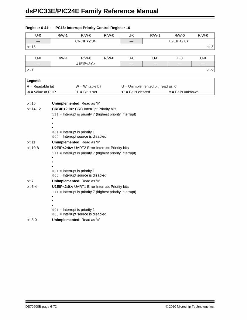
dsPIC33E/PIC24E Family Reference Manual
Register 6-41: IPC16: Interrupt Priority Control Register 16
U-0 R/W-1 R/W-0 R/W-0 U-0 R/W-1 R/W-0 R/W-0— CRCIP<2:0> — U2EIP<2:0>
bit 15 bit 8
U-0 R/W-1 R/W-0 R/W-0 U-0 U-0 U-0 U-0— U1EIP<2:0> — — — —
bit 7 bit 0
Legend:R = Readable bit W = Writable bit U = Unimplemented bit, read as ‘0’-n = Value at POR ‘1’ = Bit is set ‘0’ = Bit is cleared x = Bit is unknown
bit 15 Unimplemented: Read as ‘0’bit 14-12 CRCIP<2:0>: CRC Interrupt Priority bits
111 = Interrupt is priority 7 (highest priority interrupt)•••001 = Interrupt is priority 1000 = Interrupt source is disabled
bit 11 Unimplemented: Read as ‘0’bit 10-8 U2EIP<2:0>: UART2 Error Interrupt Priority bits
111 = Interrupt is priority 7 (highest priority interrupt)•••001 = Interrupt is priority 1000 = Interrupt source is disabled
bit 7 Unimplemented: Read as ‘0’bit 6-4 U1EIP<2:0>: UART1 Error Interrupt Priority bits
111 = Interrupt is priority 7 (highest priority interrupt)•••001 = Interrupt is priority 1000 = Interrupt source is disabled
bit 3-0 Unimplemented: Read as ‘0’
DS70600B-page 6-72 © 2010 Microchip Technology Inc.

Section 6. InterruptsInterrupts
6
Register 6-42: IPC17: Interrupt Priority Control Register 17U-0 R/W-1 R/W-0 R/W-0 U-0 R/W-1 R/W-0 R/W-0— C2TXIP<2:0> — C1TXIP<2:0>
bit 15 bit 8
U-0 R/W-1 R/W-0 R/W-0 U-0 R/W-1 R/W-0 R/W-0— DMA7IP<2:0> — DMA6IP<2:0>
bit 7 bit 0
Legend:R = Readable bit W = Writable bit U = Unimplemented bit, read as ‘0’-n = Value at POR ‘1’ = Bit is set ‘0’ = Bit is cleared x = Bit is unknown
bit 15 Unimplemented: Read as ‘0’bit 14-12 C2TXIP<2:0>: ECAN2 Transmit Data Request Interrupt Priority bits
111 = Interrupt is priority 7 (highest priority interrupt)•••001 = Interrupt is priority 1000 = Interrupt source is disabled
bit 11 Unimplemented: Read as ‘0’bit 10-8 C1TXIP<2:0>: ECAN1 Transmit Data Request Interrupt Priority bits
111 = Interrupt is priority 7 (highest priority interrupt)•••001 = Interrupt is priority 1000 = Interrupt source is disabled
bit 7 Unimplemented: Read as ‘0’bit 6-4 DMA7IP<2:0>: DMA Channel 7 Data Transfer Complete Interrupt Priority bits
111 = Interrupt is priority 7 (highest priority interrupt)•••001 = Interrupt is priority 1000 = Interrupt source is disabled
bit 3 Unimplemented: Read as ‘0’bit 2-0 DMA6IP<2:0>: DMA Channel 6 Data Transfer Complete Interrupt Priority bits
111 = Interrupt is priority 7 (highest priority interrupt)•••001 = Interrupt is priority 1000 = Interrupt source is disabled
© 2010 Microchip Technology Inc. DS70600B-page 6-73

dsPIC33E/PIC24E Family Reference Manual
Register 6-43: IPC18: Interrupt Priority Control Register 18
U-0 R/W-1 R/W-0 R/W-0 U-0 U-0 U-0 U-0— QEI2IP<2:0> — — — —
bit 15 bit 8
U-0 R/W-1 R/W-0 R/W-0 U-0 U-0 U-0 U-0— PSESMIP<2:0> — — — —
bit 7 bit 0
Legend:R = Readable bit W = Writable bit U = Unimplemented bit, read as ‘0’-n = Value at POR ‘1’ = Bit is set ‘0’ = Bit is cleared x = Bit is unknown
bit 15-11 Unimplemented: Read as ‘0’bit 11 Unimplemented: Read as ‘0’bit 10-8 FLT3IP<2:0>: PWM Fault3 Interrupt Priority bits
111 = Interrupt is priority 7 (highest priority interrupt)•••001 = Interrupt is priority 1000 = Interrupt source is disabled
bit 7 Unimplemented: Read as ‘0’bit 6-4 PSESMIP<2:0>: PWM Secondary Special Event Match Interrupt Priority bits
111 = Interrupt is priority 7 (highest priority interrupt)•••001 = Interrupt is priority 1000 = Interrupt source is disabled
bit 3-0 Unimplemented: Read as ‘0’
DS70600B-page 6-74 © 2010 Microchip Technology Inc.

Section 6. InterruptsInterrupts
6
Register 6-44: IPC20: Interrupt Priority Control Register 20U-0 R/W-1 R/W-0 R/W-0 U-0 R/W-1 R/W-0 R/W-0— U3TXIP<2:0> — U3RXIP<2:0>
bit 15 bit 8
U-0 R/W-1 R/W-0 R/W-0 U-0 U-0 U-0 U-0— U3EIP<2:0> — — — —
bit 7 bit 0
Legend:R = Readable bit W = Writable bit U = Unimplemented bit, read as ‘0’-n = Value at POR ‘1’ = Bit is set ‘0’ = Bit is cleared x = Bit is unknown
bit 15 Unimplemented: Read as ‘0’bit 14-12 U3TXIP<2:0>: UART3 TX Interrupt Priority bits
111 = Interrupt is priority 7 (highest priority interrupt)•••001 = Interrupt is priority 1000 = Interrupt source is disabled
bit 11 Unimplemented: Read as ‘0’bit 10-8 U3RXIP<2:0>: UART3 RX Interrupt Priority bits
111 = Interrupt is priority 7 (highest priority interrupt)•••001 = Interrupt is priority 1000 = Interrupt source is disabled
bit 7 Unimplemented: Read as ‘0’bit 6-4 U3EIP<2:0>: UART3 Error Interrupt Priority bits
111 = Interrupt is priority 7 (highest priority interrupt)•••001 = Interrupt is priority 1000 = Interrupt source is disabled
bit 3-0 Unimplemented: Read as ‘0’
© 2010 Microchip Technology Inc. DS70600B-page 6-75

dsPIC33E/PIC24E Family Reference Manual
Register 6-45: IPC21: Interrupt Priority Control Register 21
U-0 R/W-1 R/W-0 R/W-0 U-0 R/W-1 R/W-0 R/W-0— U4EIP<2:0> — USBIP<2:0>(1)
bit 15 bit 8
U-0 U-0 U-0 U-0 U-0 U-0 U-0 U-0— — — — — — — —
bit 7 bit 0
Legend:R = Readable bit W = Writable bit U = Unimplemented bit, read as ‘0’-n = Value at POR ‘1’ = Bit is set ‘0’ = Bit is cleared x = Bit is unknown
bit 15 Unimplemented: Read as ‘0’bit 14-12 U4EIP<2:0>: UART4 Error Interrupt Priority bits
111 = Interrupt is priority 7 (highest priority interrupt)•••001 = Interrupt is priority 1000 = Interrupt source is disabled
bit 11 Unimplemented: Read as ‘0’bit 10-8 USBIP<2:0>: USB Interrupt Priority bits(1)
111 = Interrupt is priority 7 (highest priority interrupt)•••001 = Interrupt is priority 1000 = Interrupt source is disabled
bit 7-0 Unimplemented: Read as ‘0’Note 1: This bit is enabled only in the devices with a USB module. Refer to the specific device data sheet to check
for availability of this module.
DS70600B-page 6-76 © 2010 Microchip Technology Inc.

Section 6. InterruptsInterrupts
6
Register 6-46: IPC22: Interrupt Priority Control Register 22U-0 R/W-1 R/W-0 R/W-0 U-0 R/W-1 R/W-0 R/W-0— SPI3IP<2:0> — SPI3EIP<2:0>
bit 15 bit 8
U-0 R/W-1 R/W-0 R/W-0 U-0 R/W-1 R/W-0 R/W-0— U4TXIP<2:0> — U4RXIP<2:0>
bit 7 bit 0
Legend:R = Readable bit W = Writable bit U = Unimplemented bit, read as ‘0’-n = Value at POR ‘1’ = Bit is set ‘0’ = Bit is cleared x = Bit is unknown
bit 15 Unimplemented: Read as ‘0’bit 14-12 SPI3IP<2:0>: SPI3 Interrupt Priority bits
111 = Interrupt is priority 7 (highest priority interrupt)•••001 = Interrupt is priority 1000 = Interrupt source is disabled
bit 11 Unimplemented: Read as ‘0’bit 10-8 SPI3EIP<2:0>: SPI3 Error Interrupt Priority bits
111 = Interrupt is priority 7 (highest priority interrupt)•••001 = Interrupt is priority 1000 = Interrupt source is disabled
bit 7 Unimplemented: Read as ‘0’bit 6-4 U4TXIP<2:0>: UART4 TX Interrupt Priority bits
111 = Interrupt is priority 7 (highest priority interrupt)•••001 = Interrupt is priority 1000 = Interrupt source is disabled
bit 3 Unimplemented: Read as ‘0’bit 2-0 U4RXIP<2:0>: UART4 RX Interrupt Priority bits
111 = Interrupt is priority 7 (highest priority interrupt)•••001 = Interrupt is priority 1000 = Interrupt source is disabled
© 2010 Microchip Technology Inc. DS70600B-page 6-77

dsPIC33E/PIC24E Family Reference Manual
Register 6-47: IPC23: Interrupt Priority Control Register 23
U-0 R/W-1 R/W-0 R/W-0 U-0 R/W-1 R/W-0 R/W-0— PWM2IP<2:0> — PWM1IP<2:0>
bit 15 bit 8
U-0 R/W-1 R/W-0 R/W-0 U-0 R/W-1 R/W-0 R/W-0— IC9IP<2:0> — OC9IP<2:0>
bit 7 bit 0
Legend:R = Readable bit W = Writable bit U = Unimplemented bit, read as ‘0’-n = Value at POR ‘1’ = Bit is set ‘0’ = Bit is cleared x = Bit is unknown
bit 15 Unimplemented: Read as ‘0’bit 14-12 PWM2IP<2:0>: PWM Generator 2 Interrupt Priority bits
111 = Interrupt is priority 7 (highest priority interrupt)•••001 = Interrupt is priority 1000 = Interrupt source is disabled
bit 11 Unimplemented: Read as ‘0’bit 10-8 PWM1IP<2:0>: PWM Generator 1 Interrupt Priority bits
111 = Interrupt is priority 7 (highest priority interrupt)•••001 = Interrupt is priority 1000 = Interrupt source is disabled
bit 7 Unimplemented: Read as ‘0’bit 6-4 IC9IP<2:0>: Input Capture Channel 9 Interrupt Priority bits
111 = Interrupt is priority 7 (highest priority interrupt)•••001 = Interrupt is priority 1000 = Interrupt source is disabled
bit 3 Unimplemented: Read as ‘0’bit 2-0 OC9IP<2:0>: Output Compare Channel 9 Interrupt Priority bits
111 = Interrupt is priority 7 (highest priority interrupt)•••001 = Interrupt is priority 1000 = Interrupt source is disabled
DS70600B-page 6-78 © 2010 Microchip Technology Inc.

Section 6. InterruptsInterrupts
6
Register 6-48: IPC24: Interrupt Priority Control Register 24U-0 R/W-1 R/W-0 R/W-0 U-0 R/W-1 R/W-0 R/W-0— PWM6IP<2:0> — PWM5IP<2:0>
bit 15 bit 8
U-0 R/W-1 R/W-0 R/W-0 U-0 R/W-1 R/W-0 R/W-0— PWM4IP<2:0> — PWM3IP<2:0>
bit 7 bit 0
Legend:R = Readable bit W = Writable bit U = Unimplemented bit, read as ‘0’-n = Value at POR ‘1’ = Bit is set ‘0’ = Bit is cleared x = Bit is unknown
bit 15 Unimplemented: Read as ‘0’bit 14-12 PWM6IP<2:0>: PWM Generator 6 Interrupt Priority bits
111 = Interrupt is priority 7 (highest priority interrupt)•••001 = Interrupt is priority 1000 = Interrupt source is disabled
bit 11 Unimplemented: Read as ‘0’bit 10-8 PWM5IP<2:0>: PWM Generator 5 Interrupt Priority bits
111 = Interrupt is priority 7 (highest priority interrupt)•••001 = Interrupt is priority 1000 = Interrupt source is disabled
bit 7 Unimplemented: Read as ‘0’bit 6-4 PWM4IP<2:0>: PWM Generator 4 Interrupt Priority bits
111 = Interrupt is priority 7 (highest priority interrupt)•••001 = Interrupt is priority 1000 = Interrupt source is disabled
bit 3 Unimplemented: Read as ‘0’bit 2-0 PWM3IP<2:0>: PWM Generator 3 Interrupt Priority bits
111 = Interrupt is priority 7 (highest priority interrupt)•••001 = Interrupt is priority 1000 = Interrupt source is disabled
© 2010 Microchip Technology Inc. DS70600B-page 6-79

dsPIC33E/PIC24E Family Reference Manual
Register 6-49: IPC25: Interrupt Priority Control Register 25
U-0 U-0 U-0 U-0 U-0 U-0 U-0 U-0— — — — — — — —
bit 15 bit 8
U-0 U-0 U-0 U-0 U-0 R/W-1 R/W-0 R/W-0— — — — — PWM7IP<2:0>
bit 7 bit 0
Legend:R = Readable bit W = Writable bit U = Unimplemented bit, read as ‘0’-n = Value at POR ‘1’ = Bit is set ‘0’ = Bit is cleared x = Bit is unknown
bit 15-3 Unimplemented: Read as ‘0’bit 2-0 PWM7IP<2:0>: PWM Generator 7 Interrupt Priority bits
111 = Interrupt is priority 7 (highest priority interrupt)•••001 = Interrupt is priority 1000 = Interrupt source is disabled
DS70600B-page 6-80 © 2010 Microchip Technology Inc.

Section 6. InterruptsInterrupts
6
Register 6-50: IPC29: Interrupt Priority Control Register 29U-0 R/W-1 R/W-0 R/W-0 U-0 R/W-1 R/W-0 R/W-0— DMA9IP<2:0> — DMA8IP<2:0>
bit 15 bit 8
U-0 U-0 U-0 U-0 U-0 U-0 U-0 U-0— — — — — — — —
bit 7 bit 0
Legend:R = Readable bit W = Writable bit U = Unimplemented bit, read as ‘0’-n = Value at POR ‘1’ = Bit is set ‘0’ = Bit is cleared x = Bit is unknown
bit 15 Unimplemented: Read as ‘0’bit 14-12 DMA9IP<2:0>: DMA Channel 9 Data Transfer Complete Interrupt Priority bits
111 = Interrupt is priority 7 (highest priority interrupt)•••001 = Interrupt is priority 1000 = Interrupt source is disabled
bit 11 Unimplemented: Read as ‘0’bit 10-8 DMA8IP<2:0>: DMA Channel 8 Data Transfer Complete Interrupt Priority bits
111 = Interrupt is priority 7 (highest priority interrupt)•••001 = Interrupt is priority 1000 = Interrupt source is disabled
bit 7-0 Unimplemented: Read as ‘0’
© 2010 Microchip Technology Inc. DS70600B-page 6-81

dsPIC33E/PIC24E Family Reference Manual
Register 6-51: IPC30: Interrupt Priority Control Register 30
U-0 R/W-1 R/W-0 R/W-0 U-0 R/W-1 R/W-0 R/W-0— SPI4IP<2:0> — SPI4EIP<2:0>
bit 15 bit 8
U-0 R/W-1 R/W-0 R/W-0 U-0 R/W-1 R/W-0 R/W-0— DMA11IP<2:0> — DMA10IP<2:0>
bit 7 bit 0
Legend:R = Readable bit W = Writable bit U = Unimplemented bit, read as ‘0’-n = Value at POR ‘1’ = Bit is set ‘0’ = Bit is cleared x = Bit is unknown
bit 15 Unimplemented: Read as ‘0’bit 14-12 SPI4IP<2:0>: SPI4 Interrupt Priority bits
111 = Interrupt is priority 7 (highest priority interrupt)•••001 = Interrupt is priority 1000 = Interrupt source is disabled
bit 11 Unimplemented: Read as ‘0’bit 10-8 SPI4EIP<2:0>: SPI4 Error Interrupt Priority bits
111 = Interrupt is priority 7 (highest priority interrupt)•••001 = Interrupt is priority 1000 = Interrupt source is disabled
bit 7 Unimplemented: Read as ‘0’bit 6-4 DMA11IP<2:0>: DMA Channel 11 Data Transfer Complete Interrupt Priority bits
111 = Interrupt is priority 7 (highest priority interrupt)•••001 = Interrupt is priority 1000 = Interrupt source is disabled
bit 3 Unimplemented: Read as ‘0’bit 2-0 DMA10IP<2:0>: DMA Channel 10 Data Transfer Complete Interrupt Priority bits
111 = Interrupt is priority 7 (highest priority interrupt)•••001 = Interrupt is priority 1000 = Interrupt source is disabled
DS70600B-page 6-82 © 2010 Microchip Technology Inc.

Section 6. InterruptsInterrupts
6
Register 6-52: IPC31: Interrupt Priority Control Register 31U-0 R/W-1 R/W-0 R/W-0 U-0 R/W-1 R/W-0 R/W-0— IC11IP<2:0> — OC11IP<2:0>
bit 15 bit 8
U-0 R/W-1 R/W-0 R/W-0 U-0 R/W-1 R/W-0 R/W-0— IC10IP<2:0> — OC10IP<2:0>
bit 7 bit 0
Legend:R = Readable bit W = Writable bit U = Unimplemented bit, read as ‘0’-n = Value at POR ‘1’ = Bit is set ‘0’ = Bit is cleared x = Bit is unknown
bit 15 Unimplemented: Read as ‘0’bit 14-12 IC11IP<2:0>: Input Capture Channel 11 Interrupt Priority bits
111 = Interrupt is priority 7 (highest priority interrupt)•••001 = Interrupt is priority 1000 = Interrupt source is disabled
bit 11 Unimplemented: Read as ‘0’bit 10-8 OC11IP<2:0>: Output Compare Channel 11 Interrupt Priority bits
111 = Interrupt is priority 7 (highest priority interrupt)•••001 = Interrupt is priority 1000 = Interrupt source is disabled
bit 7 Unimplemented: Read as ‘0’bit 6-4 IC10IP<2:0>: Input Capture Channel 10 Interrupt Priority bits
111 = Interrupt is priority 7 (highest priority interrupt)•••001 = Interrupt is priority 1000 = Interrupt source is disabled
bit 3 Unimplemented: Read as ‘0’bit 2-0 OC10IP<2:0>: Output Compare Channel 10 Interrupt Priority bits
111 = Interrupt is priority 7 (highest priority interrupt)•••001 = Interrupt is priority 1000 = Interrupt source is disabled
© 2010 Microchip Technology Inc. DS70600B-page 6-83

dsPIC33E/PIC24E Family Reference Manual
Register 6-53: IPC32: Interrupt Priority Control Register 32
U-0 R/W-1 R/W-0 R/W-0 U-0 R/W-1 R/W-0 R/W-0— DMA13IP<2:0> — DMA12IP<2:0>
bit 15 bit 8
U-0 R/W-1 R/W-0 R/W-0 U-0 R/W-1 R/W-0 R/W-0— IC12IP<2:0> — OC12IP<2:0>
bit 7 bit 0
Legend:R = Readable bit W = Writable bit U = Unimplemented bit, read as ‘0’-n = Value at POR ‘1’ = Bit is set ‘0’ = Bit is cleared x = Bit is unknown
bit 15 Unimplemented: Read as ‘0’bit 14-12 DMA13IP<2:0>: DMA Channel 13 Data Transfer Complete Interrupt Priority bits
111 = Interrupt is priority 7 (highest priority interrupt)•••001 = Interrupt is priority 1000 = Interrupt source is disabled
bit 11 Unimplemented: Read as ‘0’bit 10-8 DMA12IP<2:0>: DMA Channel 12 Data Transfer Complete Interrupt Priority bits
111 = Interrupt is priority 7 (highest priority interrupt)•••001 = Interrupt is priority 1000 = Interrupt source is disabled
bit 7 Unimplemented: Read as ‘0’bit 6-4 IC12IP<2:0>: Input Capture Channel 12 Interrupt Priority bits
111 = Interrupt is priority 7 (highest priority interrupt)•••001 = Interrupt is priority 1000 = Interrupt source is disabled
bit 3 Unimplemented: Read as ‘0’bit 2-0 OC12IP<2:0>: Output Compare Channel 12 Interrupt Priority bits
111 = Interrupt is priority 7 (highest priority interrupt)•••001 = Interrupt is priority 1000 = Interrupt source is disabled
DS70600B-page 6-84 © 2010 Microchip Technology Inc.

Section 6. InterruptsInterrupts
6
Register 6-54: IPC33: Interrupt Priority Control Register 33
U-0 R/W-1 R/W-0 R/W-0 U-0 R/W-1 R/W-0 R/W-0— IC13IP<2:0> — OC13IP<2:0>
bit 15 bit 8
U-0 U-0 U-0 U-0 U-0 R/W-1 R/W-0 R/W-0— — — — — DMA14IP<2:0>
bit 7 bit 0
Legend:R = Readable bit W = Writable bit U = Unimplemented bit, read as ‘0’-n = Value at POR ‘1’ = Bit is set ‘0’ = Bit is cleared x = Bit is unknown
bit 15 Unimplemented: Read as ‘0’bit 14-12 IC13IP<2:0>: Input Capture Channel 13 Interrupt Priority bits
111 = Interrupt is priority 7 (highest priority interrupt)•••001 = Interrupt is priority 1000 = Interrupt source is disabled
bit 11 Unimplemented: Read as ‘0’bit 10-8 OC13IP<2:0>: Output Compare Channel 13 Interrupt Priority bits
111 = Interrupt is priority 7 (highest priority interrupt)•••001 = Interrupt is priority 1000 = Interrupt source is disabled
bit 7-3 Unimplemented: Read as ‘0’bit 2-0 DMA14IP<2:0>: DMA Channel 14 Data Transfer Complete Interrupt Priority bits
111 = Interrupt is priority 7 (highest priority interrupt)•••001 = Interrupt is priority 1000 = Interrupt source is disabled
© 2010 Microchip Technology Inc. DS70600B-page 6-85

dsPIC33E/PIC24E Family Reference Manual
Register 6-55: IPC34: Interrupt Priority Control Register 34
U-0 R/W-1 R/W-0 R/W-0 U-0 R/W-1 R/W-0 R/W-0— IC15IP<2:0> — OC15IP<2:0>
bit 15 bit 8
U-0 R/W-1 R/W-0 R/W-0 U-0 R/W-1 R/W-0 R/W-0— IC14IP<2:0> — OC14IP<2:0>
bit 7 bit 0
Legend:R = Readable bit W = Writable bit U = Unimplemented bit, read as ‘0’-n = Value at POR ‘1’ = Bit is set ‘0’ = Bit is cleared x = Bit is unknown
bit 15 Unimplemented: Read as ‘0’bit 14-12 IC15IP<2:0>: Input Capture Channel 15 Interrupt Priority bits
111 = Interrupt is priority 7 (highest priority interrupt)•••001 = Interrupt is priority 1000 = Interrupt source is disabled
bit 11 Unimplemented: Read as ‘0’bit 10-8 OC15IP<2:0>: Output Compare Channel 15 Interrupt Priority bits
111 = Interrupt is priority 7 (highest priority interrupt)•••001 = Interrupt is priority 1000 = Interrupt source is disabled
bit 7 Unimplemented: Read as ‘0’bit 6-4 IC14IP<2:0>: Input Capture Channel 14 Interrupt Priority bits
111 = Interrupt is priority 7 (highest priority interrupt)•••001 = Interrupt is priority 1000 = Interrupt source is disabled
bit 3 Unimplemented: Read as ‘0’bit 2-0 OC14IP<2:0>: Output Compare Channel 14 Interrupt Priority bits
111 = Interrupt is priority 7 (highest priority interrupt)•••001 = Interrupt is priority 1000 = Interrupt source is disabled
DS70600B-page 6-86 © 2010 Microchip Technology Inc.

Section 6. InterruptsInterrupts
6
Register 6-56: IPC35: Interrupt Priority Control Register 35
U-0 U-0 U-0 U-0 U-0 R/W-1 R/W-0 R/W-0— — — — — ICDIP<2:0>
bit 15 bit 8
U-0 R/W-1 R/W-0 R/W-0 U-0 R/W-1 R/W-0 R/W-0— IC16IP<2:0> — OC16IP<2:0>
bit 7 bit 0
Legend:R = Readable bit W = Writable bit U = Unimplemented bit, read as ‘0’-n = Value at POR ‘1’ = Bit is set ‘0’ = Bit is cleared x = Bit is unknown
bit 15-11 Unimplemented: Read as ‘0’bit 10-8 ICDIP<2:0>: ICD Interrupt Priority bits
111 = Interrupt is priority 7 (highest priority interrupt)•••001 = Interrupt is priority 1000 = Interrupt source is disabled
bit 7 Unimplemented: Read as ‘0’bit 6-4 IC16IP<2:0>: Input Capture Channel 16 Interrupt Priority bits
111 = Interrupt is priority 7 (highest priority interrupt)•••001 = Interrupt is priority 1000 = Interrupt source is disabled
bit 3 Unimplemented: Read as ‘0’bit 2-0 OC16IP<2:0>: Output Compare Channel 16 Interrupt Priority bits
111 = Interrupt is priority 7 (highest priority interrupt)•••001 = Interrupt is priority 1000 = Interrupt source is disabled
© 2010 Microchip Technology Inc. DS70600B-page 6-87

dsPIC33E/PIC24E Family Reference Manual
Register 6-57: INTTREG: Interrupt Control and Status Register
U-0 U-0 U-0 U-0 R-0 R-0 R-0 R-0— — — — ILR<3:0>
bit 15 bit 8
R-0 R-0 R-0 R-0 R-0 R-0 R-0 R-0VECNUM<7:0>
bit 7 bit 0
Legend:R = Readable bit W = Writable bit U = Unimplemented bit, read as ‘0’-n = Value at POR ‘1’ = Bit is set ‘0’ = Bit is cleared x = Bit is unknown
bit 15-12 Unimplemented: Read as ‘0’bit 11-8 ILR<3:0>: New CPU Interrupt Priority Level bits
1111 = CPU Interrupt Priority Level is 15•••0001 = CPU Interrupt Priority Level is 10000 = CPU Interrupt Priority Level is 0
bit 7-0 VECNUM<7:0>: Vector Number of Pending Interrupt bits11111111 = Interrupt vector pending is number 263•••00000001 = Interrupt vector pending is number 900000000 = Interrupt vector pending is number 8
DS70600B-page 6-88 © 2010 Microchip Technology Inc.

Section 6. InterruptsInterrupts
6
6.5 INTERRUPT SETUP PROCEDURES6.5.1 InitializationTo configure an interrupt source, complete the following steps:
1. If nested interrupts are not desired, set the NSTDIS control bit (INTCON1<15>).2. Select the user application-assigned priority level for the interrupt source by writing the
control bits in the appropriate IPCx Control register. The priority level depends on thespecific application and type of the interrupt source. If multiple priority levels are not desired,the IPCx register control bits for all enabled interrupt sources can be programmed to thesame non-zero value.
3. Clear the interrupt flag status bit associated with the peripheral in the associated IFSxStatus register.
4. Enable the interrupt source by setting the interrupt enable control bit associated with thesource in the appropriate IECx Control register.
6.5.2 Interrupt Service RoutineThe method used to declare an ISR and initialize the IVT with the correct vector address dependson the programming language (C or Assembler) and the language development tool suite usedto develop the application.
In general, the user application must clear the interrupt flag in the appropriate IFSx register forthe source of interrupt that the ISR handles. Otherwise, the application will re-enter the ISRimmediately after it exits the routine. If the ISR is coded in Assembler language, it must beterminated using a RETFIE instruction to unstack the saved PC value, SRL value and old CPUpriority level.
6.5.3 Trap Service RoutineA TSR is coded like an ISR, except that the appropriate trap status flag in the INTCON1 registermust be cleared to avoid re-entry into the TSR.
6.5.4 Interrupt DisableTo enable user interrupts, set the GIE bit in the INTCON2 register. To disable interrupts, clear theGIE bit in the INTCON2 register.
The DISI instruction provides a convenient way to disables interrupts of priority levels 1-6 for afixed period of time. Level 7 interrupt sources are not disabled by the DISI instruction.
Note: At a device Reset, the IPC registers are initialized such that all user interruptsources are assigned to priority level 4.
Note: Only user interrupts with a priority level of 7 or less can be disabled. Trap sources(level 8-level 15) cannot be disabled.
© 2010 Microchip Technology Inc. DS70600B-page 6-89

dsPIC33E/PIC24E Family Reference Manual
6.5.5 Code ExampleExample 6-1 illustrates the code sequence that enables nested interrupts, sets up Timer1,Timer2, Timer3, Timer4 and change notice peripherals to priority levels 2, 5, 6, 3 and 4,respectively. It also illustrates how interrupts can be enabled and disabled using the Statusregister. Sample ISR illustrates interrupt clearing.
Example 6-1: Interrupt Setup Code Examplevoid enableInterrupts(void){
/* Enable level 1-7 interrupts *//* No restoring of previous CPU IPL state performed here */INTCON2bits.GIE = 1;
return;}
void disableInterrupts(void){
/* Disable level 1-7 interrupts *//* No saving of current CPU IPL setting performed here */
INTCON2bits.GIE = 0;
return;}
void initInterrupts(void){
/* Interrupt nesting enabled here */INTCON1bits.NSTDIS = 0;
/* Set Timer3 interrupt priority to 6 (level 7 is highest) */IPC2bits.T3IP = 6;
/* Set Timer2 interrupt priority to 5 */IPC1bits.T2IP = 5;
/* Set Change Notice interrupt priority to 4 */IPC4bits.CNIP = 4;
/* Set Timer4 interrupt priority to 3 */IPC6bits.T4IP = 3;
/* Set Timer1 interrupt priority to 2 */IPC0bits.T1IP = 2;
/* Reset Timer1 interrupt flag */IFS0bits.T1IF = 0;
/* Reset Timer2 interrupt flag */IFS0bits.T2IF = 0;
/* Reset Timer3 interrupt flag */IFS0bits.T3IF = 0;
/* Reset Timer4 interrupt flag */IFS1bits.T4IF = 0;
/* Enable CN interrupts */IEC1bits.CNIE = 1;
DS70600B-page 6-90 © 2010 Microchip Technology Inc.

Section 6. InterruptsInterrupts
6
Example 6-1: Interrupt Setup Code Example (Continued)/* Enable Timer1 interrupt */IEC0bits.T1IE = 1;
/* Enable Timer2 interrupt (PWM time base) */IEC0bits.T2IE = 1;
/* Enable Timer3 interrupt */IEC0bits.T3IE = 1;
/* Enable Timer4 interrupt (replacement for Timer 2 */IEC1bits.T4IE = 1;
/* Reset change notice interrupt flag */IFS1bits.CNIF = 0;
return;}
void __attribute__((__interrupt__,no_auto_psv)) _T1Interrupt(void){
/* Insert ISR Code Here*/
/* Clear Timer1 interrupt */IFS0bits.T1IF = 0;
}
void __attribute__((__interrupt__,no_auto_psv)) _T2Interrupt(void){
/* Insert ISR Code Here*/
/* Clear Timer2 interrupt */IFS0bits.T2IF = 0;
}
void __attribute__((__interrupt__,no_auto_psv)) _T3Interrupt(void){
/* Insert ISR Code Here*/
/* Clear Timer3 interrupt */IFS0bits.T3IF = 0;
}
void __attribute__((__interrupt__,no_auto_psv)) _T4Interrupt(void){
/* Insert ISR Code Here*/
/* Clear Timer4 interrupt */IFS1bits.T4IF = 0;
}
void __attribute__((__interrupt__,no_auto_psv)) _CNInterrupt(void){
/* Insert ISR Code Here*/
/* Clear CN interrupt */IFS1bits.CNIF = 0;
}
© 2010 Microchip Technology Inc. DS70600B-page 6-91

dsPIC33E/PIC
24E Family R
eference Manual
DS
70600B-page 6-92
© 2010 M
icrochip Technology Inc.
e is provided in Table 6-2.
Bit 3 Bit 2 Bit 1 Bit 0 AllResets
RR ADDRERR STKERR OSCFAIL — 0000
P INT3EP INT2EP INT1EP INT0EP 8000
R — — — — 0000
— — — SGHT 0000
IF T1IF OC1IF IC1IF INT0IF 0000
F CNIF CMIF MI2C1IF SI2C1IF 0000
IF C1IF C1RXIF SPI2IF SPI2EIF 0000
T8IF MI2C2IF SI2C2IF T7IF 0000
IF CRCIF U2EIF U1EIF — 0000
U3TXIF U3RXIF U3EIF — 0000
IF PWM6IF PWM5IF PWM4IF PWM3IF 0000
— — — — 0000
IF DMA13IF DMA12IF IC12IF OC12IF 0000
IE T1IE OC1IE IC1IE INT0IE 0000
E CNIE CMIE MI2C1IE SI2C1IE 0000
IE C1IE C1RXIE SPI2IE SPI2EIE 0000
T8IE MI2C2IE SI2C2IE T7IE 0000
IE CRCIE U2EIE U1EIE — 0000
U3TXIE U3RXIE U3EIE — 0000
IE PWM6IE PWM5IE PWM4IE PWM3IE 0000
— — — — 0000
IE DMA13IE DMA12IE IC12IE OC12IE 0000
— INT0IP<2:0> 4444
— DMA0IP<2:0> 4444
— T3IP<2:0> 4444
— U1TXIP<2:0> 4444
— SI2C1IP<2:0> 4444
— INT1IP<2:0> 4444
— DMA2IP<2:0> 4444
— T5IP<2:0> 4444
— SPI2EIP<2:0> 4444
6.6 REGISTER MAPA summary of the registers associated with the dsPIC33E/PIC24E family Interrupts modul
Table 6-2: Interrupt Controller Register Map(1)
File Name Bit 15 Bit 14 Bit 13 Bit 12 Bit 11 Bit 10 Bit 9 Bit 8 Bit 7 Bit 6 Bit 5 Bit 4
INTCON1 NSTDIS OVAERR OVBERR COVAERR COVBERR OVATE OVBTE COVTE SFTACERR DIV0ERR DMACTRAP MATHE
INTCON2 GIE DISI SWTRAP — — — — — — — — INT4E
INTCON3 — — — — — — — — — UAE DAE DOOV
INTCON4 — — — — — — — — — — — —
IFS0 NVMIF DMA1IF AD1IF U1TXIF U1RXIF SPI1IF SPI1EIF T3IF T2IF OC2IF IC2IF DMA0
IFS1 U2TXIF U2RXIF INT2IF T5IF T4IF OC4IF OC3IF DMA2IF IC8IF IC7IF AD2IF INT1I
IFS2 T6IF DMA4IF PMPIF OC8IF OC7IF OC6IF OC5IF IC6IF IC5IF IC4IF IC3IF DMA3
IFS3 — RTCIF DMA5IF DCIIF DCIEIF QEI1IF PSEMIF C2IF C2RXIF INT4IF INT3IF T9IF
IFS4 — — — — QEI2IF — PSESMIF — C2TXIF C1TXIF DMA7IF DMA6
IFS5 PWM2IF PWM1IF IC9IF OC9IF SPI3IF SPI3EIF U4TXIF U4RXIF U4EIF USBIF — —
IFS6 — — — — — — — — — — — PWM7
IFS7 IC11IF OC11IF IC10IF OC10IF SPI4IF SPI4EIF DMA11IF DMA10IF DMA9IF DMA8IF — —
IFS8 — ICDIF IC16IF OC16IF IC15IF OC15IF IC14IF OC14IF IC13IF OC13IF — DMA14
IEC0 NVMIE DMA1IE AD1IE U1TXIE U1RXIE SPI1IE SPI1EIE T3IE T2IE OC2IE IC2IE DMA0
IEC1 U2TXIE U2RXIE INT2IE T5IE T4IE OC4IE OC3IE DMA2IE IC8IE IC7IE AD2IE INT1I
IEC2 T6IE DMA4IE PMPIE OC8IE OC7IE OC6IE OC5IE IC6IE IC5IE IC4IE IC3IE DMA3
IEC3 — RTCIE DMA5IE DCIIE DCIEIE QEI1IE PSEMIE C2IE C2RXIE INT4IE INT3IE T9IE
IEC4 — — — — QEI2IE — PSESMIE — C2TXIE C1TXIE DMA7IE DMA6
IEC5 PWM2IE PWM1IE IC9IE OC9IE SPI3IE SPI3EIE U4TXIE U4RXIE U4EIE USBIE — —
IEC6 — — — — — — — — — — — PWM7
IEC7 IC11IE OC11IE IC10IE OC10IE SPI4IE SPI4EIE DMA11IE DMA10IE DMA9IE DMA8IE — —
IEC8 — ICDIE IC16IE OC16IE IC15IE OC15IE IC14IE OC14IE IC13IE OC13IE — DMA14
IPC0 — T1IP<2:0> — OC1IP<2:0> — IC1IP<2:0>
IPC1 — T2IP<2:0> — OC2IP<2:0> — IC2IP<2:0>
IPC2 — U1RXIP<2:0> — SPI1IP<2:0> — SPI1EIP<2:0>
IPC3 — NVMIP<2:0> — DMA1IP<2:0> — AD1IP<2:0>
IPC4 — CNIP<2:0> — CMIP<2:0> — MI2C1IP<2:0>
IPC5 — IC8IP<2:0> — IC7IP<2:0> — AD2IP<2:0>
IPC6 — T4IP<2:0> — OC4IP<2:0> — OC3IP<2:0>
IPC7 — U2TXIP<2:0> — U2RXIP<2:0> — INT2IP<2:0>
IPC8 — C1IP<2:0> — C1RXIP<2:0> — SPI2IP<2:0>
Legend: — = unimplemented, read as ‘0’. Reset values are shown in hexadecimal.Note 1: Not all bits are available for all devices. Please refer to the specific device data sheet for availability.

© 2010 M
icrochip Technology Inc.D
S70600B
-page 6-93
Section 6. InterruptsInterrupts 6
IP — DMA3IP<2:0> 4444
IP — IC6IP<2:0> 4444
IP — OC8IP<2:0> 4444
IP — T7IP<2:0> 4444
IP — T9IP<2:0> 4444
IP — C2IP<2:0> 4444
IP — DCIIP<2:0> 0444
IP — — — — 4440
IP — DMA6IP<2:0> 4444
IP — — — — 4040
IP — — — — 4440
IP — — — — 4400
IP — U4RXIP<2:0> 4444
IP — OC9IP<2:0> 4444
IP — PWM3IP<2:0> 4444
IP — PWM7IP<2:0> 0004
IP — — — — 4400
IP — DMA10IP<2:0> 4444
IP — OC10IP<2:0> 4444
IP — OC12IP<2:0> 4444
IP — DMA14IP<2:0> 4404
IP — OC14IP<2:0> 4444
IP — OC16IP<2:0> 0444
IN 7:0> 0000
Ta
N Bit 3 Bit 2 Bit 1 Bit 0 AllResets
LeNo
C9 — IC5IP<2:0> — IC4IP<2:0> — IC3IP<2:0>
C10 — OC7IP<2:0> — OC6IP<2:0> — OC5IP<2:0>
C11 — T6IP<2:0> — DMA4IP<2:0> — PMPIP<2:0>
C12 — T8IP<2:0> — MI2C2IP<2:0> — SI2C2IP<2:0>
C13 C2RXIP<2:0> — INT4IP<2:0> — INT3IP<2:0>
C14 — DCIEIP<2:0> — QEI1IP<2:0> — PSESMIP<2:0>
C15 — — — — — RTCIP<2:0> — DMA5IP<2:0>
C16 — CRCIP<2:0> — U2EIP<2:0> — U1EIP<2:0>
C17 — C2TXIP<2:0> — C1TXIP<2:0> — DMA7IP<2:0>
C18 — QEI2IP<2:0> — — — — — PSEMIP<2:0>
C20 — U3TXIP<2:0> — U3RXIP<2:0> — U3EIP<2:0>
C21 — U4EIP<2:0> — USBIP<2:0> — — — —
C22 — SPI3IP<2:0> — SPI3EIP<2:0> — U4TXIP<2:0>
C23 — PWM2IP<2:0> — PWM1IP<2:0> — IC9IP<2:0>
C24 — PWM6IP<2:0> — PWM5IP<2:0> — PWM4IP<2:0>
C25 — — — — — — — — — — — —
C29 — DMA9IP<2:0> — DMA8IP<2:0> — — — —
C30 — SPI4IP<2:0> — SPI4EIP<2:0> — DMA11IP<2:0>
C31 — IC11IP<2:0> — OC11IP<2:0> — IC10IP<2:0>
C32 — DMA13IP<2:0> — DMA12IP<2:0> — IC12IP<2:0>
C33 — IC13IP<2:0> — OC13IP<2:0> — — — —
C34 — IC15IP<2:0> — OC15IP<2:0> — IC14IP<2:0>
C35 — — — — — ICDIP<2:0> — IC16IP<2:0>
TTREG — — — — ILR<3:0> VECNUM<
ble 6-2: Interrupt Controller Register Map(1) (Continued)File ame Bit 15 Bit 14 Bit 13 Bit 12 Bit 11 Bit 10 Bit 9 Bit 8 Bit 7 Bit 6 Bit 5 Bit 4
gend: — = unimplemented, read as ‘0’. Reset values are shown in hexadecimal.te 1: Not all bits are available for all devices. Please refer to the specific device data sheet for availability.
dsPIC33E/PIC24E Family Reference Manual
6.7 DESIGN TIPS
Question 1: What happens when two sources of interrupt become pending at the sametime and have the same user application-assigned priority level?
Answer: The interrupt source with the highest natural order priority will take precedence.The natural order priority is determined by the IVT address for that source.Interrupt sources with a lower IVT address have a higher natural order priority.
Question 2: Can the DISI instruction be used to disable all sources of interrupt andtraps?
Answer: The DISI instruction does not disable traps or priority level 7 interrupt sources.However, the DISI instruction can be used as a convenient way to disable allinterrupt sources, if no priority level 7 interrupt sources are enabled in the user’sapplication.
Question 3: What happens when a peripheral interrupt is used as a DMA request?Answer: The user application can designate any peripheral interrupt to be a DMA request.
A DMA request is an IRQ that is directed to the DMA. When the DMA channel isconfigured to respond to a particular interrupt as a DMA request, the applicationshould disable the corresponding CPU interrupt. Otherwise, a CPU interruptwould also be requested.
DS70600B-page 6-94 © 2010 Microchip Technology Inc.

Section 6. InterruptsInterrupts
6
6.8 RELATED APPLICATION NOTESThis section lists application notes that are related to this section of the manual. Theseapplication notes may not be written specifically for the dsPIC33E/PIC24E product family, but theconcepts are pertinent and could be used with modification and possible limitations. The currentapplication notes related to the Interrupts module are:
Title Application Note #No related application notes at this time.
Note: Please visit the Microchip web site (www.microchip.com) for additional ApplicationNotes and code examples for the dsPIC33E/PIC24E family of devices.
© 2010 Microchip Technology Inc. DS70600B-page 6-95

dsPIC33E/PIC24E Family Reference Manual
6.9 REVISION HISTORY
Revision A (July 2009)This is the initial released version of this document.
Revision B (April 2010)This revision includes the following global updates that occur throughout the document:
• Bit name changes (see also Table 6-2: Interrupt Controller Register Map):- DMACTRAP is now DMACERR (see Register 6-3)- CMPIF is now CMIF (see Register 6-8)- PCEPIF is now PSEMIF (see Register 6-10)- PCESIF is now PSESMIF (see Register 6-11)- CMPIE is now CMIE (see Register 6-17)- RTCCIE is now RTCIE and PCEPIE is now PSEMIE (see Register 6-19)- PCESIE is now PSESMIE (see Register 6-20)- CMPIP is now CMIP (see Register 6-29)- PCEPIP is now PSEMIP (see Register 6-39)- RTCCIP is now RTCIP (see Register 6-40)- PCEPIP is now PSESMIP (see Register 6-43)
Additional updates include the following:
• Added the following new sections:- 6.2.1.4.1 “USB Address Error Soft Trap (UAE)”- 6.2.1.4.2 “DMA Address Error Soft Trap (DAE)”- 6.2.1.4.3 “DO Stack Overflow Soft Trap (DOOVR)”)
• Updated the five void __attribute lines of code and removed the watermark from the Interrupt Setup Code example (see Example 6-1)
• Updated the following Interrupt Source names in Table 6-1:- CMP1 is now CM (see Interrupt Vector Number 26)- PCEP is now PSEM – PWM Special Event Match (see Interrupt Vector Number 65)- RTCC is now RTC (see Interrupt Vector Number 70)- PCES is now PSESM – PWM Secondary Special Event Match (see Interrupt Vector
Number 81)- SI2C3 is now Reserved (see Interrupt Vector Number 95)- MI2C3 is now Reserved (see Interrupt Vector Number 96)- USBOIG is now USB1 (see Interrupt Vector Number 97)- PCG1 through PCG7 are now PWM1 through PWM7 (see Interrupt Vector Numbers
105 through 111)• Register additions and deletions (see also Table 6-2: Interrupt Controller Register Map):
- Added a definition for the VAR bit in Register 6-2- Added a shaded note to clarify hard trap operation in 6.2.2.4 “Generic Hard Trap”- Changed the default POR value for the GIE bit from ‘0’ to ‘1’ in the Interrupt Control
Register 2 (see Register 6-4)- Removed the FLT1IF bit from IFS3 (see Register 6-10)- Added the CRCIF bit and removed the FLT4IF, FLT3IF, and FLT2IF bits from IFS4 (see
Register 6-11)- Removed the MI2C3IF and SI2C3IF bits from IFS5 (see Register 6-12)- Removed the PWM9IF and PWM7IF bits from IFS6 (see Register 6-13)- Added the ICDIF and DMA12IF bits to IFS8 (see Register 6-15)- Removed the FLT1IE bit from IEC3 (see Register 6-19)- Removed the FLT4IE and FLT3IE bits from IEC4 (see Register 6-20)- Removed the PWM9IE and PWM8IE bits from IEC6 (see Register 6-22)
DS70600B-page 6-96 © 2010 Microchip Technology Inc.

Section 6. InterruptsInterrupts
6
Revision B (April 2010) (Continued)• Register additions and deletions (Continued) (see also Table 6-2: Interrupt ControllerRegister Map):- Added the ICDIE and DMA12IE bits to IEC8 (see Register 6-24)- Removed the FLT1IP<2:0> bits from IPC15 (see Register 6-40)- Removed the FLT2IP<2:0> bits from IPC16 (see Register 6-41)- Removed the FLT3IP<2:0> bits from IPC18 (see Register 6-43)- Removed IPC19 (was Register 6-44)- Removed the MI2C3IP<2:0> and SI2C3IP<2:0> bits from IPC21 (see Register 6-45)- Added the ICDIP<2:0> bits to IPC35 (see Register 6-56)- Updated the VECNUM bits from <6:0> to <7:0> in INTTREG (see Register 6-57)
© 2010 Microchip Technology Inc. DS70600B-page 6-97

dsPIC33E/PIC24E Family Reference Manual
NOTES:
DS70600B-page 6-98 © 2010 Microchip Technology Inc.

Note the following details of the code protection feature on Microchip devices:• Microchip products meet the specification contained in their particular Microchip Data Sheet.
• Microchip believes that its family of products is one of the most secure families of its kind on the market today, when used in the intended manner and under normal conditions.
• There are dishonest and possibly illegal methods used to breach the code protection feature. All of these methods, to our knowledge, require using the Microchip products in a manner outside the operating specifications contained in Microchip’s Data Sheets. Most likely, the person doing so is engaged in theft of intellectual property.
• Microchip is willing to work with the customer who is concerned about the integrity of their code.
• Neither Microchip nor any other semiconductor manufacturer can guarantee the security of their code. Code protection does not mean that we are guaranteeing the product as “unbreakable.”
Code protection is constantly evolving. We at Microchip are committed to continuously improving the code protection features of ourproducts. Attempts to break Microchip’s code protection feature may be a violation of the Digital Millennium Copyright Act. If such actsallow unauthorized access to your software or other copyrighted work, you may have a right to sue for relief under that Act.
Information contained in this publication regarding deviceapplications and the like is provided only for your convenienceand may be superseded by updates. It is your responsibility toensure that your application meets with your specifications.MICROCHIP MAKES NO REPRESENTATIONS ORWARRANTIES OF ANY KIND WHETHER EXPRESS ORIMPLIED, WRITTEN OR ORAL, STATUTORY OROTHERWISE, RELATED TO THE INFORMATION,INCLUDING BUT NOT LIMITED TO ITS CONDITION,QUALITY, PERFORMANCE, MERCHANTABILITY ORFITNESS FOR PURPOSE. Microchip disclaims all liabilityarising from this information and its use. Use of Microchipdevices in life support and/or safety applications is entirely atthe buyer’s risk, and the buyer agrees to defend, indemnify andhold harmless Microchip from any and all damages, claims,suits, or expenses resulting from such use. No licenses areconveyed, implicitly or otherwise, under any Microchipintellectual property rights.
© 2010 Microchip Technology Inc.
Trademarks
The Microchip name and logo, the Microchip logo, dsPIC, KEELOQ, KEELOQ logo, MPLAB, PIC, PICmicro, PICSTART, PIC32 logo, rfPIC and UNI/O are registered trademarks of Microchip Technology Incorporated in the U.S.A. and other countries.
FilterLab, Hampshire, HI-TECH C, Linear Active Thermistor, MXDEV, MXLAB, SEEVAL and The Embedded Control Solutions Company are registered trademarks of Microchip Technology Incorporated in the U.S.A.
Analog-for-the-Digital Age, Application Maestro, CodeGuard, dsPICDEM, dsPICDEM.net, dsPICworks, dsSPEAK, ECAN, ECONOMONITOR, FanSense, HI-TIDE, In-Circuit Serial Programming, ICSP, Mindi, MiWi, MPASM, MPLAB Certified logo, MPLIB, MPLINK, mTouch, Octopus, Omniscient Code Generation, PICC, PICC-18, PICDEM, PICDEM.net, PICkit, PICtail, REAL ICE, rfLAB, Select Mode, Total Endurance, TSHARC, UniWinDriver, WiperLock and ZENA are trademarks of Microchip Technology Incorporated in the U.S.A. and other countries.
SQTP is a service mark of Microchip Technology Incorporated in the U.S.A.
All other trademarks mentioned herein are property of their respective companies.
© 2010, Microchip Technology Incorporated, Printed in the U.S.A., All Rights Reserved.
Printed on recycled paper.
ISBN: 978-1-60932-130-7
DS70600B-page 99
Microchip received ISO/TS-16949:2002 certification for its worldwide headquarters, design and wafer fabrication facilities in Chandler and Tempe, Arizona; Gresham, Oregon and design centers in California and India. The Company’s quality system processes and procedures are for its PIC® MCUs and dsPIC® DSCs, KEELOQ® code hopping devices, Serial EEPROMs, microperipherals, nonvolatile memory and analog products. In addition, Microchip’s quality system for the design and manufacture of development systems is ISO 9001:2000 certified.

WORLDWIDE SALES AND SERVICE
DS70600B-page 100 © 2010 Microchip Te
AMERICASCorporate Office2355 West Chandler Blvd.Chandler, AZ 85224-6199Tel: 480-792-7200 Fax: 480-792-7277Technical Support: http://support.microchip.comWeb Address: www.microchip.comAtlantaDuluth, GA Tel: 678-957-9614 Fax: 678-957-1455BostonWestborough, MA Tel: 774-760-0087 Fax: 774-760-0088ChicagoItasca, IL Tel: 630-285-0071 Fax: 630-285-0075ClevelandIndependence, OH Tel: 216-447-0464 Fax: 216-447-0643DallasAddison, TX Tel: 972-818-7423 Fax: 972-818-2924DetroitFarmington Hills, MI Tel: 248-538-2250Fax: 248-538-2260KokomoKokomo, IN Tel: 765-864-8360Fax: 765-864-8387Los AngelesMission Viejo, CA Tel: 949-462-9523 Fax: 949-462-9608Santa ClaraSanta Clara, CA Tel: 408-961-6444Fax: 408-961-6445TorontoMississauga, Ontario, CanadaTel: 905-673-0699 Fax: 905-673-6509
ASIA/PACIFICAsia Pacific OfficeSuites 3707-14, 37th FloorTower 6, The GatewayHarbour City, KowloonHong KongTel: 852-2401-1200Fax: 852-2401-3431Australia - SydneyTel: 61-2-9868-6733Fax: 61-2-9868-6755China - BeijingTel: 86-10-8528-2100 Fax: 86-10-8528-2104China - ChengduTel: 86-28-8665-5511Fax: 86-28-8665-7889China - ChongqingTel: 86-23-8980-9588Fax: 86-23-8980-9500China - Hong Kong SARTel: 852-2401-1200 Fax: 852-2401-3431China - NanjingTel: 86-25-8473-2460Fax: 86-25-8473-2470China - QingdaoTel: 86-532-8502-7355Fax: 86-532-8502-7205China - ShanghaiTel: 86-21-5407-5533 Fax: 86-21-5407-5066China - ShenyangTel: 86-24-2334-2829Fax: 86-24-2334-2393China - ShenzhenTel: 86-755-8203-2660 Fax: 86-755-8203-1760China - WuhanTel: 86-27-5980-5300Fax: 86-27-5980-5118China - XianTel: 86-29-8833-7252Fax: 86-29-8833-7256China - XiamenTel: 86-592-2388138 Fax: 86-592-2388130China - ZhuhaiTel: 86-756-3210040 Fax: 86-756-3210049
ASIA/PACIFICIndia - BangaloreTel: 91-80-3090-4444 Fax: 91-80-3090-4123India - New DelhiTel: 91-11-4160-8631Fax: 91-11-4160-8632India - PuneTel: 91-20-2566-1512Fax: 91-20-2566-1513Japan - YokohamaTel: 81-45-471- 6166 Fax: 81-45-471-6122Korea - DaeguTel: 82-53-744-4301Fax: 82-53-744-4302Korea - SeoulTel: 82-2-554-7200Fax: 82-2-558-5932 or 82-2-558-5934Malaysia - Kuala LumpurTel: 60-3-6201-9857Fax: 60-3-6201-9859Malaysia - PenangTel: 60-4-227-8870Fax: 60-4-227-4068Philippines - ManilaTel: 63-2-634-9065Fax: 63-2-634-9069SingaporeTel: 65-6334-8870Fax: 65-6334-8850Taiwan - Hsin ChuTel: 886-3-6578-300Fax: 886-3-6578-370Taiwan - KaohsiungTel: 886-7-536-4818Fax: 886-7-536-4803Taiwan - TaipeiTel: 886-2-2500-6610 Fax: 886-2-2508-0102Thailand - BangkokTel: 66-2-694-1351Fax: 66-2-694-1350
EUROPEAustria - WelsTel: 43-7242-2244-39Fax: 43-7242-2244-393Denmark - CopenhagenTel: 45-4450-2828 Fax: 45-4485-2829France - ParisTel: 33-1-69-53-63-20 Fax: 33-1-69-30-90-79Germany - MunichTel: 49-89-627-144-0 Fax: 49-89-627-144-44Italy - Milan Tel: 39-0331-742611 Fax: 39-0331-466781Netherlands - DrunenTel: 31-416-690399 Fax: 31-416-690340Spain - MadridTel: 34-91-708-08-90Fax: 34-91-708-08-91UK - WokinghamTel: 44-118-921-5869Fax: 44-118-921-5820
01/05/10
chnology Inc.