scanning electron microscope
DESCRIPTION
Guidelines to understanding and operating SEM instrumentTRANSCRIPT

Introduction to Scanning Electron Microscopy
By: Brandon Cheney
Ant’s Leg Integrated Circuit
Nano-composite
This document was created as part of a Senior Project in the Materials Engineering
Department at San Jose State University. It is intended to provide an introduction scanning electron microscopy and techniques for better imaging. References are provided at the end of the paper for those who wish to study the subject more thoroughly.
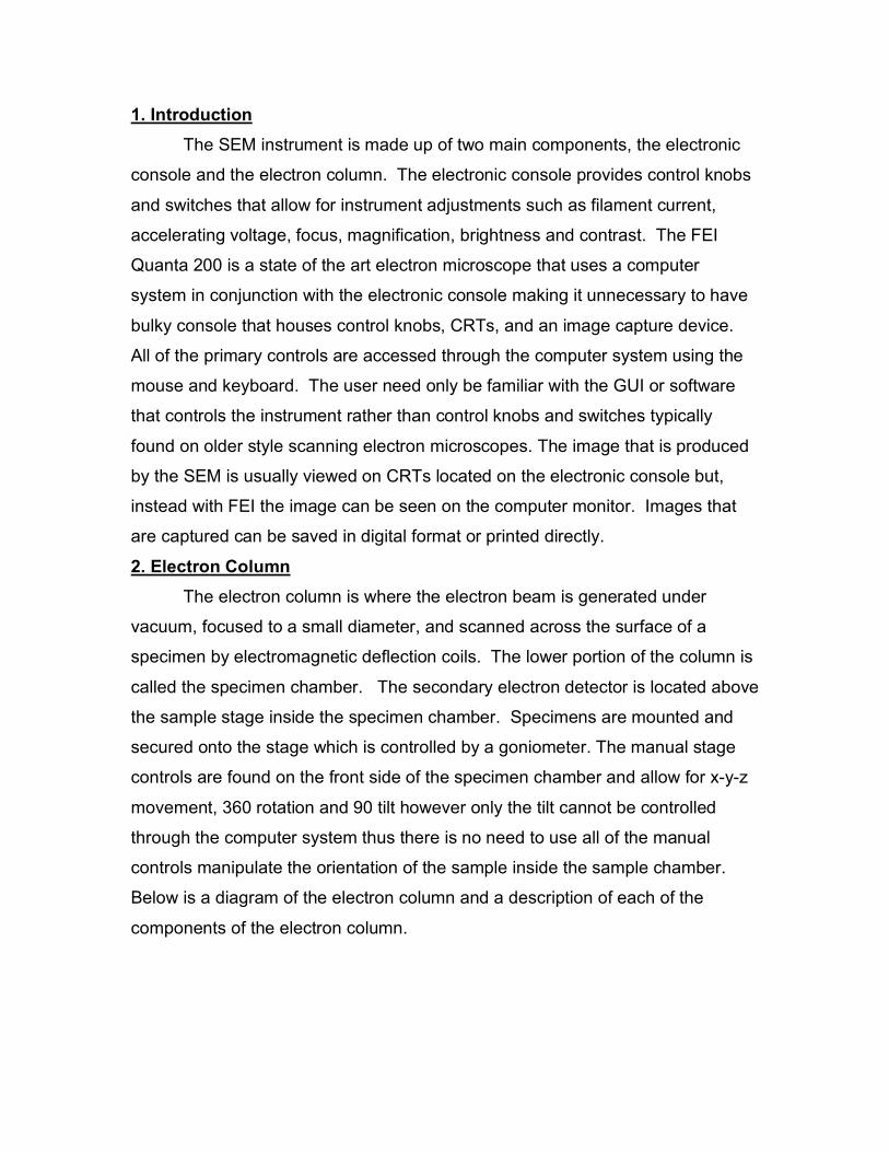
1. Introduction The SEM instrument is made up of two main components, the electronic
console and the electron column. The electronic console provides control knobs
and switches that allow for instrument adjustments such as filament current,
accelerating voltage, focus, magnification, brightness and contrast. The FEI
Quanta 200 is a state of the art electron microscope that uses a computer
system in conjunction with the electronic console making it unnecessary to have
bulky console that houses control knobs, CRTs, and an image capture device.
All of the primary controls are accessed through the computer system using the
mouse and keyboard. The user need only be familiar with the GUI or software
that controls the instrument rather than control knobs and switches typically
found on older style scanning electron microscopes. The image that is produced
by the SEM is usually viewed on CRTs located on the electronic console but,
instead with FEI the image can be seen on the computer monitor. Images that
are captured can be saved in digital format or printed directly.
2. Electron Column The electron column is where the electron beam is generated under
vacuum, focused to a small diameter, and scanned across the surface of a
specimen by electromagnetic deflection coils. The lower portion of the column is
called the specimen chamber. The secondary electron detector is located above
the sample stage inside the specimen chamber. Specimens are mounted and
secured onto the stage which is controlled by a goniometer. The manual stage
controls are found on the front side of the specimen chamber and allow for x-y-z
movement, 360 rotation and 90 tilt however only the tilt cannot be controlled
through the computer system thus there is no need to use all of the manual
controls manipulate the orientation of the sample inside the sample chamber.
Below is a diagram of the electron column and a description of each of the
components of the electron column.

Figure 2. Scanning electron microscope column [1].
1) Electron gun: Located at the top of the column where free electrons are
generated by thermionic emission from a tungsten filament at ~2700K.
The filament is inside the Wehnelt which controls the number of electrons
leaving the gun. Electrons are primarily accelerated toward an anode that
is adjustable from 200V to 30 kV (1kV=1000V).
2) Condenser Lenses: After the beam passes the anode it is influenced by
two condenser lenses that cause the beam to converge and pass through
a focal point. What occurs is that the electron beam is essentially focused
down to 1000 times its original size. In conjunction with the selected
accelerating voltage the condenser lenses are primarily responsible for
determining the intensity of the electron beam when it strikes the
specimen [1].

3) Apertures: Depending on the microscope one or more apertures may be
found in the electron column. The function of these apertures is to reduce
and exclude extraneous electrons in the lenses. The final lens aperture
located below the scanning coils determines the diameter or spot size of
the beam at the specimen. The spot size on the specimen will in part
determine the resolution and depth of field. Decreasing the spot size will
allow for an increase in resolution and depth of field with a loss of
brightness [1].
4) Scanning System: Images are formed by rastering the electron beam
across the specimen using deflection coils inside the objective lens. The
stigmator or astigmatism corrector is located in the objective lens and
uses a magnetic field in order to reduce aberrations of the electron beam.
The electron beam should have a circular cross section when it strikes the
specimen however it is usually elliptical thus the stigmator acts to control
this problem [1,4].
5) Specimen Chamber: At the lower portion of the column the specimen
stage and controls are located. The secondary electrons from the
specimen are attracted to the detector by a positive charge.
3. Vacuum System
The ability for a SEM to provide a controlled electron beam requires that
the electronic column be under vacuum at a pressure of at least 5x10⁻⁵ Torr. A
high vacuum pressure is required for a variety of reasons. First, the current that
passes through the filament causes the filament to reach temperatures around
2700K [2]. A hot tungsten filament will oxidize and burn out in the presence of air
at atmospheric pressure. Secondly, the ability of the column optics to operate
properly requires a fairly clean, dust-free environment. Third, air particles and
dust inside the column can interfere and block the electrons before the ever
reach the specimen in the sample chamber [1]. In order to provide adequate
vacuum pressure inside the column, a vacuum system consisting of two or more
pumps is typically present.

Separate pumps are required because one pump isn’t really capable of
doing all the work but, in conjunction they can provide a good vacuum pressure
relatively quickly and efficiently. A majority of the initial pumping is done by the
action of a mechanical pump often called a roughing pump. The roughing pump
operates first during the pump-down process and has excellent efficiency above
10-2 Torr. Although many mechanical pumps used in SEMs are capable of
producing pressures better than 5x10⁻⁵ Torr, a very long pump down time would
mostly be required. Pressures lower than 10-2 Torr are more easily acquired by
the action of a turbo-molecular pump. Turbo-molecular pumps make use of a
turbine that rotates at 20,000 to 50,000 rotations per minute to evacuate gas
molecules and particulates found inside the column [7]. Turbo-molecular pumps
are expensive and sensitive to vibrations thus it is important to remember that
sudden jolts to the instrument can not only affect the beam but, the severely
damage turbo pumps.
The FEI Quanta 200 is design to operate in three separate vacuum
modes, high vacuum (10-6 to 10-7 Torr), low vacuum (0.1 to 20 Torr) and ESEM
(0.1 to 20 Torr) [6]. In the low vacuum and ESEM mode of operation the
pressure inside the specimen chamber operates at a lower pressure than that
inside the actual column which is always at high vacuum. The high vacuum mode
is typically where most SEMs operate. In this mode the highest resolutions and
magnifications can be achieved although, it is not suitable for all specimens.
Generally anything that is conductive and has a high density works well in high
vacuum mode. Specimens that are non-conductive or have a low density are
more suitable for the low vacuum or ESEM mode. The ESEM mode of operation
is necessary for wet, non-conductive samples.
4. Electron Beam-Specimen Interactions
Originally microscopy was based on the use of the light microscope and
could provide specimen resolutions on the order of 0.2 microns. To achieve
higher resolutions, an electron source is required instead of light as the
illumination source, which allows for resolutions of about 25 Angstroms. The use

of electrons not only gives better resolution but, due to the nature electron beam
specimen interactions there are a variety of signals that can be used to provide
information regarding characteristics at and near the surface of a specimen.
In scanning electron microscopy visual inspection of the surface of a
material utilizes signals of two types, secondary and backscattered electrons.
Secondary and backscattered electrons are constantly being produced from the
surface of the specimen while under the electron beam however they are a result
of two separate types of interaction. Secondary electrons are a result of the
inelastic collision and scattering of incident electrons with specimen electrons.
They are generally characterized by possessing energies of less than 50 eV [1].
They are used to reveal the surface structure of a material with a resolution of
~10 nm or better [1].
Backscattered electrons are a result of an elastic collision and scattering
event between incident electrons and specimen nuclei or electrons.
Backscattered electrons can be generated further from the surface of the
material and help to resolve topographical contrast and atomic number contrast
with a resolution of >1 micron. While there are several types of signals that are
generated from a specimen under an electron beam the x-ray signal is typically
the only other signal that is used for scanning electron microscopy. The x-ray
signal is a result of recombination interactions between free electrons and
positive electron holes that are generated within the material. The x-ray signal
can originate from further down into the surface of the specimen surface and
allows for determination of elemental composition through EDS (energy
dispersive x-ray spectroscopy) analysis of characteristic x-ray signals. Figure 3
is a diagram which displays a cross section of the volume of primary excitation
illustrating zones from which signals may be detected [1].

Figure 3. Signals that result from electron beam-specimen interaction [2].
5. Observation Techniques
Scanning microscopes are becoming much easier to use these days with
the advancement of electronics and introduction of new techniques. After just a
short amount of training nearly anybody can acquire relatively good images. As
users begin to investigate a broader range of materials and encounter more
complex analysis scenarios, satisfactory images become more difficult for the
inexperienced user to obtain. When the image is not clear enough or an image
of a particular feature is seemingly impossible to obtain, it requires further
problem solving to determine what the cause really is. This section will focus on
the techniques for successful imaging.

Image Disturbances
There are many types of image disturbances that occur while imaging
specimens. In some cases these disturbances are attributed to defects with the
instrument; however, more than likely the disturbances are due to operator’s lack
of experience, improper sample preparation, or external influences such as
instrument vibration. Disturbances can be examined and corrected using a
systematic approach based on their appearance. Table 2 below summarizes
image disturbances and conditions that might cause them.
Table 2. Image disturbances and their possible causes [6].

Effect of Accelerating Voltage
The accelerating voltage on the Qunata 200 is adjustable from
200V-30 kV. Choosing the right accelerating voltage is critical for obtaining a
good clear image however the most suitable voltage level depends will depend
on mostly on the type of material being examined. The more conductive the
material the better it will behave under higher voltages. Higher voltages (15-
30kv) generally allow for high resolution at high magnifications although, this can
damage the specimen very quickly if it is not highly conductive. Thus, when
imaging polymers and ceramics it is more suitable to use voltages below 10 kV.
The figure below details the effect of using high and low accelerating voltages.
Figure 4. Effect of accelerating voltage [6].

5 kV Accelerating Voltage 25 kV Accelerating Voltage
Figure 5. The above images were taken at different accelerating voltages, notice how the resolution is improved with increased accelerating voltage [6].
30 kV Accelerating Voltage 5 kV Accelerating Voltage
Figure 6. The above images were with different accelerating voltages, notice how surface structures appear clearer at lower voltages [6].

Effect of Working Distance
Besides the accelerating voltage one’s choice of working distance and
spot size will greatly influence the image quality. As with accelerating voltage
there exists a give and take situation when choosing the most suitable settings
for working distance and spot size. Generally speaking a working distance of
10mm should be used and will allow for a good depth of field while maintaining
good resolution. In most cases one may want to reduce the working distance to
achieve better resolution especially when using lower accelerating voltages.
Figure 5 below illustrates the effect of working distance.
Figure 7. Effect of working distance [6].
10 mm Working Distance 38 mm Working Distance
Figure 8. The above images were taken at two different working distances, notice how the depth of field increases with working distance [6].

Effect of Spot Size
Spot size basically restricts the beam current and will thereby cause for
brightness and contrast compensations. Smaller spot sizes will require higher
brightness and contrast levels thus there can be a limits when using a small spot
size. Typically smaller spot sizes allow for higher resolution and a greater depth
of field. Figure 6 below shows the effects of spot size on image quality.
Figure 9. Effect of Spot Size [6].
600 micron spot size 200 micron spot size
Figure 10. The above images were taken with two different size spot sizes. Notice how much the depth of field is improved in the 200 micron spot size image [6].

6. References
1. M.T. Postek, K.S. Howard, A.H. Johnson and K.L. McMichael, Scanning Electron Microscopy: A Student’s Handbook, (Ladd Research Ind., Inc. Williston, VT., 1980).
2. C.E. Lyman, D.E. Newbury, J.I. Goldstein, D.B. Williams, A.D. Romig, J.T.
Armstrong, P. Echlin, C.E. Fiori, D.C. Joy, E. Lifshin and Klaus-Ruediger Peters, Scanning Electron Microscopy, X-Ray Microanalysis and Analytical Electron Microscopy: A Laboratory Workbook, (Plenum Press. New York, N.Y., 1990).
3. J.I. Goldstein, H. Yakowitz, D.E. Newbury, E. Lifshin, J.W. Colby, J.W.
Colby and J.R. Coleman, Pratical Scanning Electron Microscopy: Electron and Ion Microprobe Analysis, edited by J.I. Goldstein and H. Yakowitz (Pelnum Press. New York, N.Y., 1975).
4. I.M. Watt, The Principles and Practice of Electron Microscopy, (Cambridge
Univ. Press. Cambridge, England, 1985).
5. FEI. The Quanta 200 User’s Operation Manual 2nd ed. (2004).
6. JEOL. Guide to scanning electron Microscopy [Online]. Available at http://www.jeol.com/sem/docs/sem_guide/tbcontd.html (accessed 1 Feb 2005).
7. WIKIPEDIA (2005). Turbo molecular pump [Online]. Available at
http://en.wikipedia.org/wiki/Turbomolecular_pump (accessed 1 Feb 2005).