saw-less direct conversion receiver consideration
TRANSCRIPT

Author : Criterion
Why do we need external filter
In most wireless radios a weak desired signal can be accompanied by interferers
that can be significantly stronger[1]. For example, as liiustrated below, if phone1
transmits maximum GSM power, i.e. 33 dBm. Let’s assume the antenna efficiency
of phone1 and phone2 are both 50%(i.e. 3dB loss). Consequently, the phone2
receiver circuit will suffer from 0 dBm interferer.
We usually call the strong interferer blocker or jammer.
1

Author : Criterion
Blockers can drastically degrade the receiver performance through compressing
its gain and hence increasing its noise figure, as shown below[3] :
As shown below[8], stronger the blocker, more the gain reduction.
2

Author : Criterion
According to cascade noise figure formula[4,6] :
In general, less the LNA gain, higher the noise figure and worse the sensitivity.
Take SKY74092-11 of SKYWORKS for example, its P1dB is -5 dBm, and may be
saturated by the 0 dBm blocker as mentioned above[2].
3
Author : Criterion
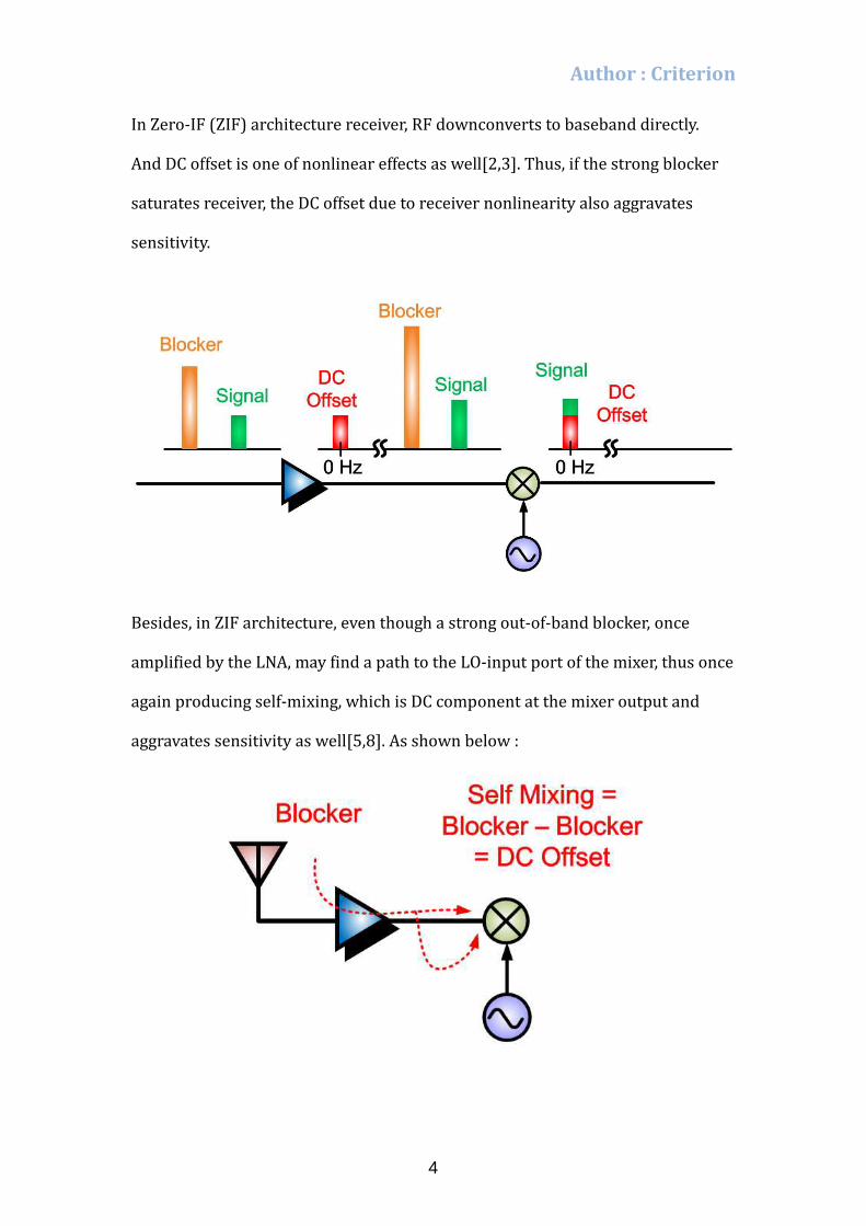
In Zero-IF (ZIF) architecture receiver, RF downconverts to baseband directly.
And DC offset is one of nonlinear effects as well[2,3]. Thus, if the strong blocker
saturates receiver, the DC offset due to receiver nonlinearity also aggravates
sensitivity.
Besides, in ZIF architecture, even though a strong out-of-band blocker, once
amplified by the LNA, may find a path to the LO-input port of the mixer, thus once
again producing self-mixing, which is DC component at the mixer output and
aggravates sensitivity as well[5,8]. As shown below :
4
Author : Criterion
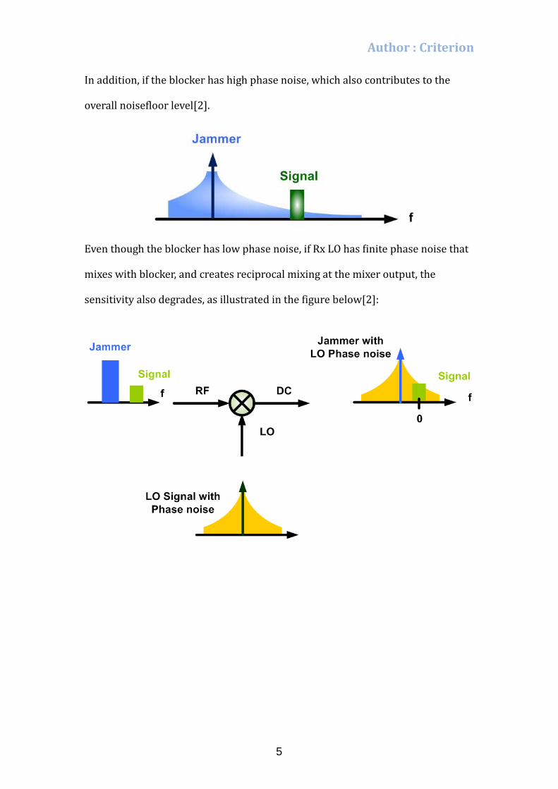
In addition, if the blocker has high phase noise, which also contributes to the
overall noisefloor level[2].
Even though the blocker has low phase noise, if Rx LO has finite phase noise that
mixes with blocker, and creates reciprocal mixing at the mixer output, the
sensitivity also degrades, as illustrated in the figure below[2]:
5
Author : Criterion
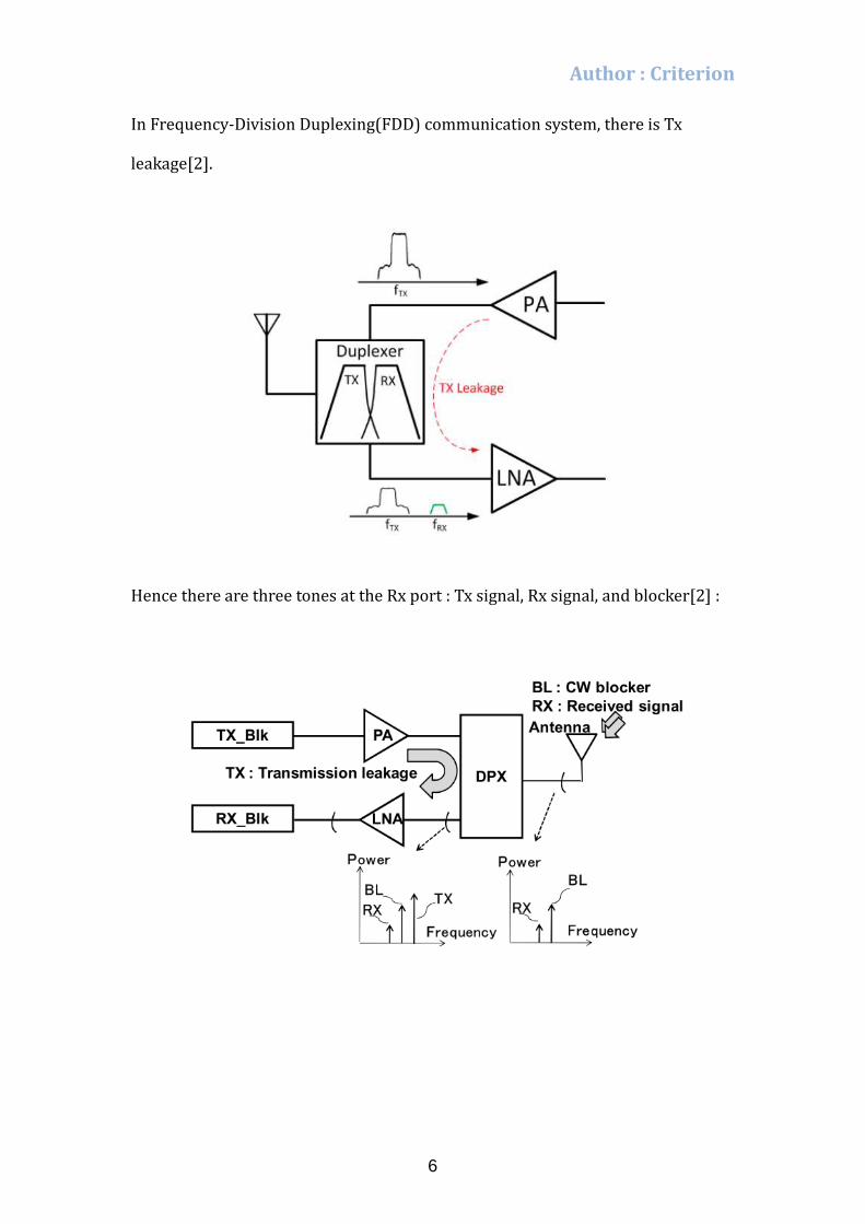
In Frequency-Division Duplexing(FDD) communication system, there is Tx
leakage[2].
Hence there are three tones at the Rx port : Tx signal, Rx signal, and blocker[2] :
6
Author : Criterion
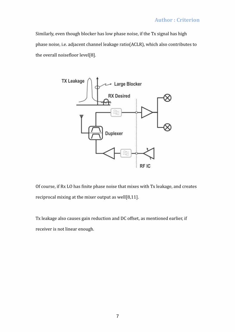
Similarly, even though blocker has low phase noise, if the Tx signal has high
phase noise, i.e. adjacent channel leakage ratio(ACLR), which also contributes to
the overall noisefloor level[8].
Of course, if Rx LO has finite phase noise that mixes with Tx leakage, and creates
reciprocal mixing at the mixer output as well[8,11].
Tx leakage also causes gain reduction and DC offset, as mentioned earlier, if
receiver is not linear enough.
7
Author : Criterion
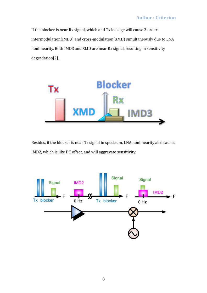
If the blocker is near Rx signal, which and Tx leakage will cause 3 order
intermodulation(IMD3) and cross-modulation(XMD) simultaneously due to LNA
nonlinearity. Both IMD3 and XMD are near Rx signal, resulting in sensitivity
degradation[2].
Besides, if the blocker is near Tx signal in spectrum, LNA nonlinearity also causes
IMD2, which is like DC offset, and will aggravate sensitivity.
8

Author : Criterion
Thus, the blocker and Tx leakage may affect the receiver by following
products[6] :
As mentioned above, we already know the effects from Tx leakage and blocker.
Higher the Tx leakage and blocker, higher the noise figure[7,14] :
9

Author : Criterion
Especially, if the mobile station is at the edge of the cellular boundary and there
is a strong blocker presence, due to the power control, the mobile's transmitter
power is kept close to it's maximum level maintain communication quality[2].
And the mobile station receives extremely weak signal in this case[13].
10
Author : Criterion
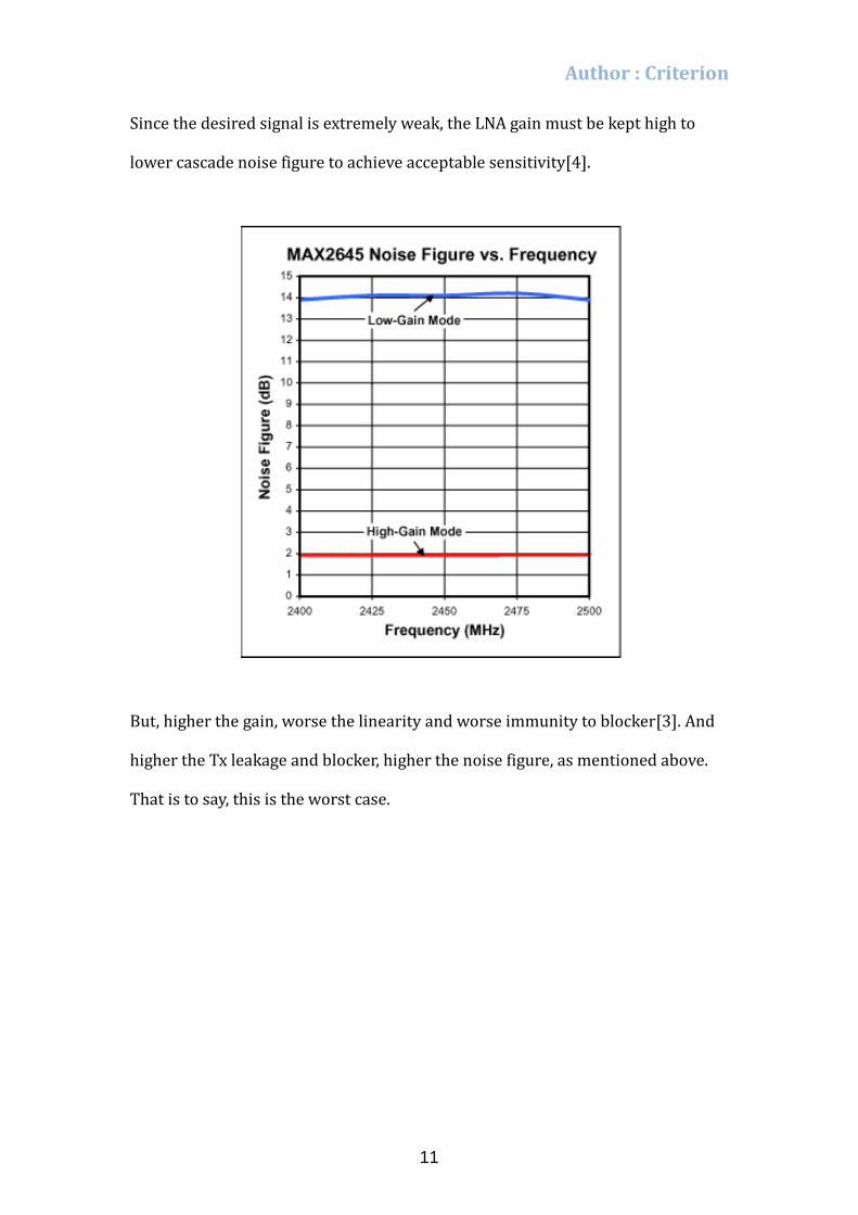
Since the desired signal is extremely weak, the LNA gain must be kept high to
lower cascade noise figure to achieve acceptable sensitivity[4].
But, higher the gain, worse the linearity and worse immunity to blocker[3]. And
higher the Tx leakage and blocker, higher the noise figure, as mentioned above.
That is to say, this is the worst case.
11

Author : Criterion
Hence in most standards, the receiver must satisfy a certain blocking template
defined at various blocker frequencies and levels, to insure sensitivity with
blocker. For instance, in the GSM standard, a desired signal only 3 dB above the
sensitivity could be accompanied by an out-of-band blocker as large as 0 dBm,
and as close as only 80 MHz to the edge of the PCS band[6,12].
Therefore, the blocker must be filtered out prior to reaching the LNA, especially
with high gain mode[1]. For these reasons, all existing receivers inevitably use an
external SAW filter at the LNA input to reject out-of-band blocker[7].
12

Author : Criterion
Although WCDMA scheme proves to be more resilient to out-of-band blockers,
due to the spread-spectrum nature of the system[10].
But as mentioned earlier, FDD communication system has Tx leakage issue. In
principle, the duplexer is effectively a dual-band highly selective filter, isolating
the RX and TX bands. However, cost and size constraints play the major role,
especially in multi-band applications, and limit the duplexer performance. As a
result, the duplexer isolation is finite, on the order of 45 to 50 dB, and the
receiver is plagued by the transmitter signal, as mentioned earlier. Less the
isolation, stronger the Tx leakage and worse the sensitivity. Generally speaking,
the duplexer isolation should be at least 55dB[2].
13
Author : Criterion
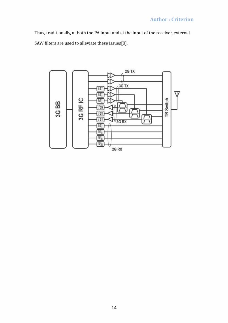
Thus, traditionally, at both the PA input and at the input of the receiver, external
SAW filters are used to alleviate these issues[8].
14
Author : Criterion
Why do we wanna remove external
filter
Nevertheless, since the external filters are typically not tunable, in multi-mode or
multi-band applications, each band requires a dedicated filter[8]. And this has
several obvious disadvantages.
First, it increases the cost, especially in multi-mode and multi-band applications,
where several of these filters are needed.
Second, according to cascade noise figure formula[4], the insertion loss of the
SAW filter, typically as high as 2 to 3 dB, degrades the receiver sensitivity
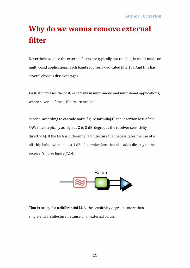
directly[4]. If the LNA is differential architecture that necessitates the use of a
off-chip balun with at least 1 dB of insertion loss that also adds directly to the
receiver’s noise figure[7,14].
That is to say, for a differential LNA, the sensitivity degrades more than
single-end architecture because of an external balun.
15
Author : Criterion
In order to overcome the loss of the external SAW filter and balun at the receiver
input, perhaps an external LNA is required[3], which helps to achieve a lower
noise figure. But an external LNA increases the cost as well, and it may degrade
the receiver’s linearity due to its inherent gain[3].
Third, the presence of these filters removes the flexibility of sharing the LNAs in
multi-mode or multi-band applications, particularly in software-defined
radios[8,9].
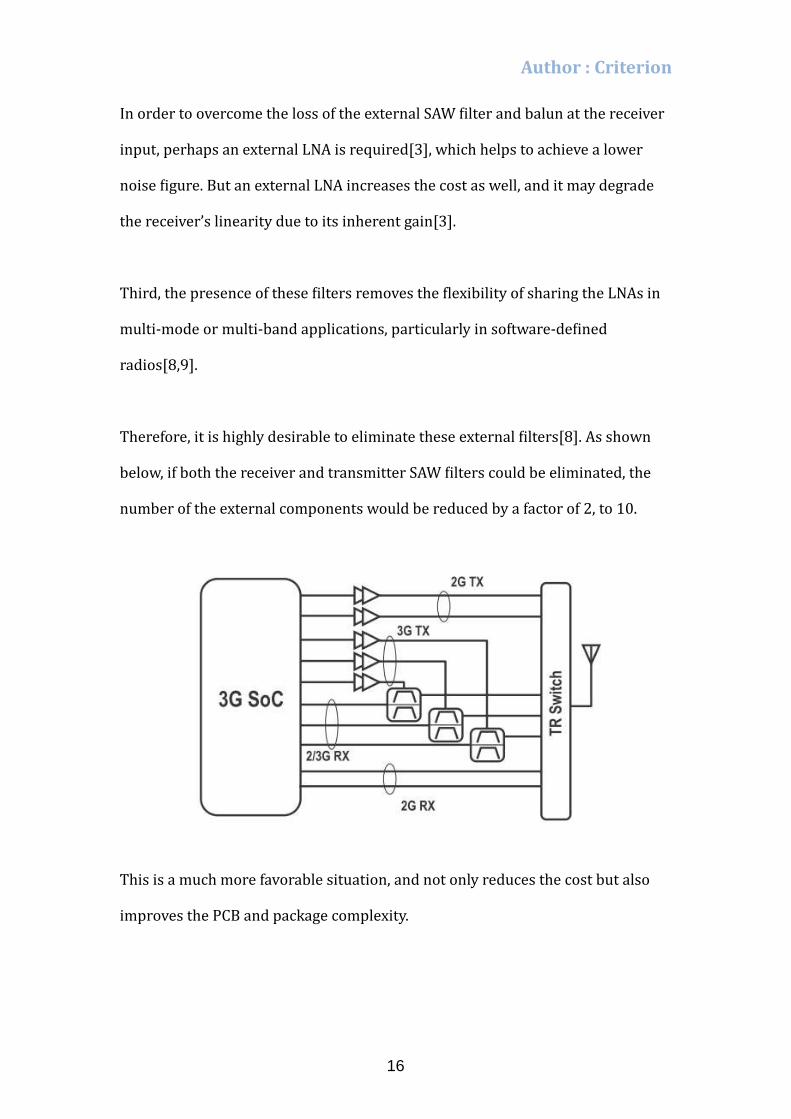
Therefore, it is highly desirable to eliminate these external filters[8]. As shown
below, if both the receiver and transmitter SAW filters could be eliminated, the
number of the external components would be reduced by a factor of 2, to 10.
This is a much more favorable situation, and not only reduces the cost but also
improves the PCB and package complexity.
16

Author : Criterion
The risk of removing external filter
However, eliminating RF filtering is challenging, this comes at the cost of more
stringent requirements of linearity for both receiver and transmitter[7,8]. As
indicated earlier, removing the receiver SAW filter reduces the receiver immunity
to strong out-of-band blockers that saturate LNA and aggravate sensitivity. In
FDD communication system, TX leakage mixes with an out-of-band blocker.
Due to the nonlinearity of the receiver, the IMD and XMD products will fall in the
desired receiver channel. These effects are typically relaxed by placing an
external SAW filter at the receiver to further attenuate the transmitter leakage
and out-of-band blockers. Otherwise, both the isolation of duplexer and the
nonlinearity requirements would be very stringent. Depending on the duplexer
isolation in the TX band, it can be shown that with typical blocker levels specified
in the 3GPP standard, this could lead to an IIP3 requirement of somewhere
around − 5 to 5 dBm[2,8].
17
Author : Criterion
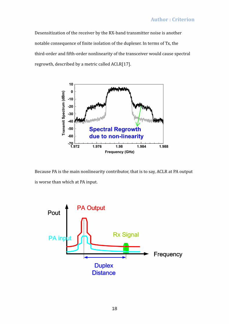
Desensitization of the receiver by the RX-band transmitter noise is another
notable consequence of finite isolation of the duplexer. In terms of Tx, the
third-order and fifth-order nonlinearity of the transceiver would cause spectral
regrowth, described by a metric called ACLR[17].
Because PA is the main nonlinearity contributor, that is to say, ACLR at PA output
is worse than which at PA input.
18
Author : Criterion
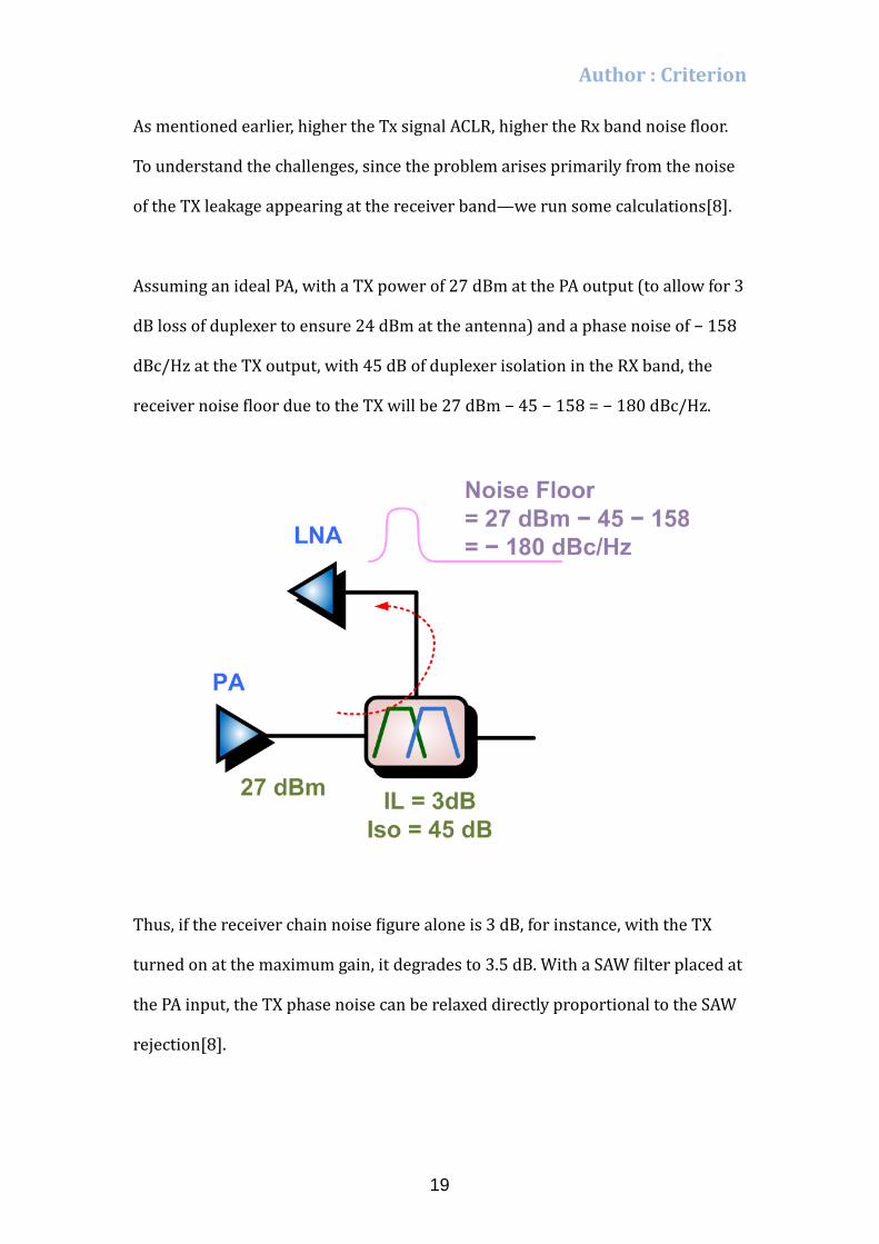
As mentioned earlier, higher the Tx signal ACLR, higher the Rx band noise floor.
To understand the challenges, since the problem arises primarily from the noise
of the TX leakage appearing at the receiver band—we run some calculations[8].
Assuming an ideal PA, with a TX power of 27 dBm at the PA output (to allow for 3
dB loss of duplexer to ensure 24 dBm at the antenna) and a phase noise of − 158
dBc/Hz at the TX output, with 45 dB of duplexer isolation in the RX band, the
receiver noise floor due to the TX will be 27 dBm − 45 − 158 = − 180 dBc/Hz.
Thus, if the receiver chain noise figure alone is 3 dB, for instance, with the TX
turned on at the maximum gain, it degrades to 3.5 dB. With a SAW filter placed at
the PA input, the TX phase noise can be relaxed directly proportional to the SAW
rejection[8].
19
Author : Criterion
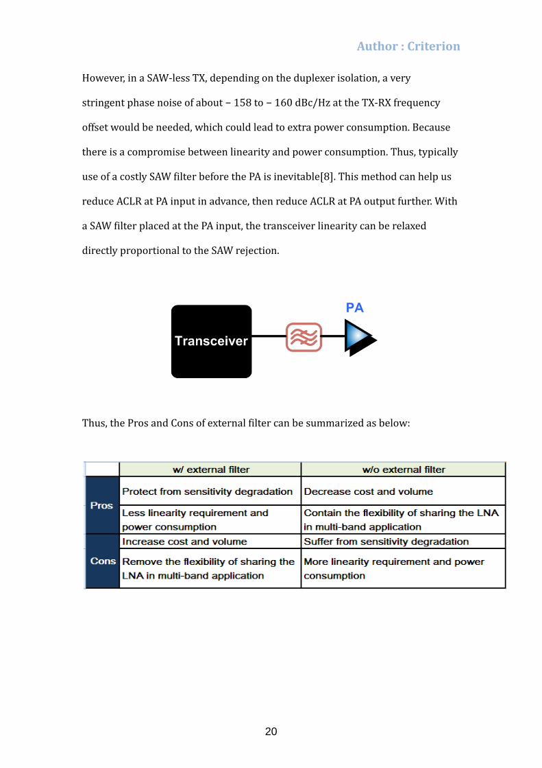
However, in a SAW-less TX, depending on the duplexer isolation, a very
stringent phase noise of about − 158 to − 160 dBc/Hz at the TX-RX frequency
offset would be needed, which could lead to extra power consumption. Because
there is a compromise between linearity and power consumption. Thus, typically
use of a costly SAW filter before the PA is inevitable[8]. This method can help us
reduce ACLR at PA input in advance, then reduce ACLR at PA output further. With
a SAW filter placed at the PA input, the transceiver linearity can be relaxed
directly proportional to the SAW rejection.
Thus, the Pros and Cons of external filter can be summarized as below:
20

Author : Criterion
Blocker-Tolerant techniques
Although external filters can reject out-of-band blockers. Nevertheless, not all
blockers can be eliminated by external filter, explained briefly as follows.
As shown above, an external SAW filter can eliminate out-of-band blockers and
Tx leakage, but can’t eliminate in-band blockers, which is ultimately through
baseband filtering[8,11]. And the nonlinear effects aggravating sensitivity, e.g.
gain reduction, DC offset, self-mixing, phase noise, IMD, and reciprocal mixing,
can be caused by in-band blockers as well.
21

Author : Criterion
As mentioned above, eliminating external filters can contain the flexibility of
sharing the LNAs in multi-mode or multi-band applications. Take ALM-1106 of
AVAGO for example, it can implemented in GPS/ISM/Wimax applications
simultaneously. Due to its wideband characteristic (0.9-3.5 GHz frequency
range), it is suitable for wideband application[9].
But compared to narrowband design, a wideband receiver can’t employ external
RF filtering and, therefore, a large blocker will saturate a conventional front-end
design. Besides, since external filtering has been ruled out, a conventional
wideband design has no selectivity and amplifies both the wanted signal and any
blockers. Any blocker present (whether or not it causes gain compression) will
be downconverted along with the wanted signal.
Consequently, for wideband or SAW-less design, the receivers need to be
considered blocker-tolerant[7]. And there are mainly three ways :
(1). Improve the receiver and transmitter linearity
(2). On-chip filtering
(3). Improve the isolation of duplexer
22
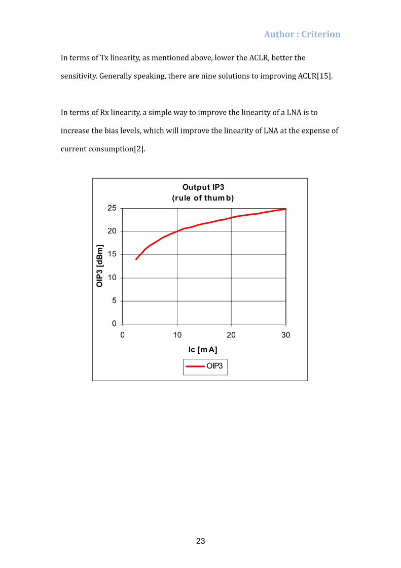
Author : Criterion
In terms of Tx linearity, as mentioned above, lower the ACLR, better the
sensitivity. Generally speaking, there are nine solutions to improving ACLR[15].
In terms of Rx linearity, a simple way to improve the linearity of a LNA is to
increase the bias levels, which will improve the linearity of LNA at the expense of
current consumption[2].
23
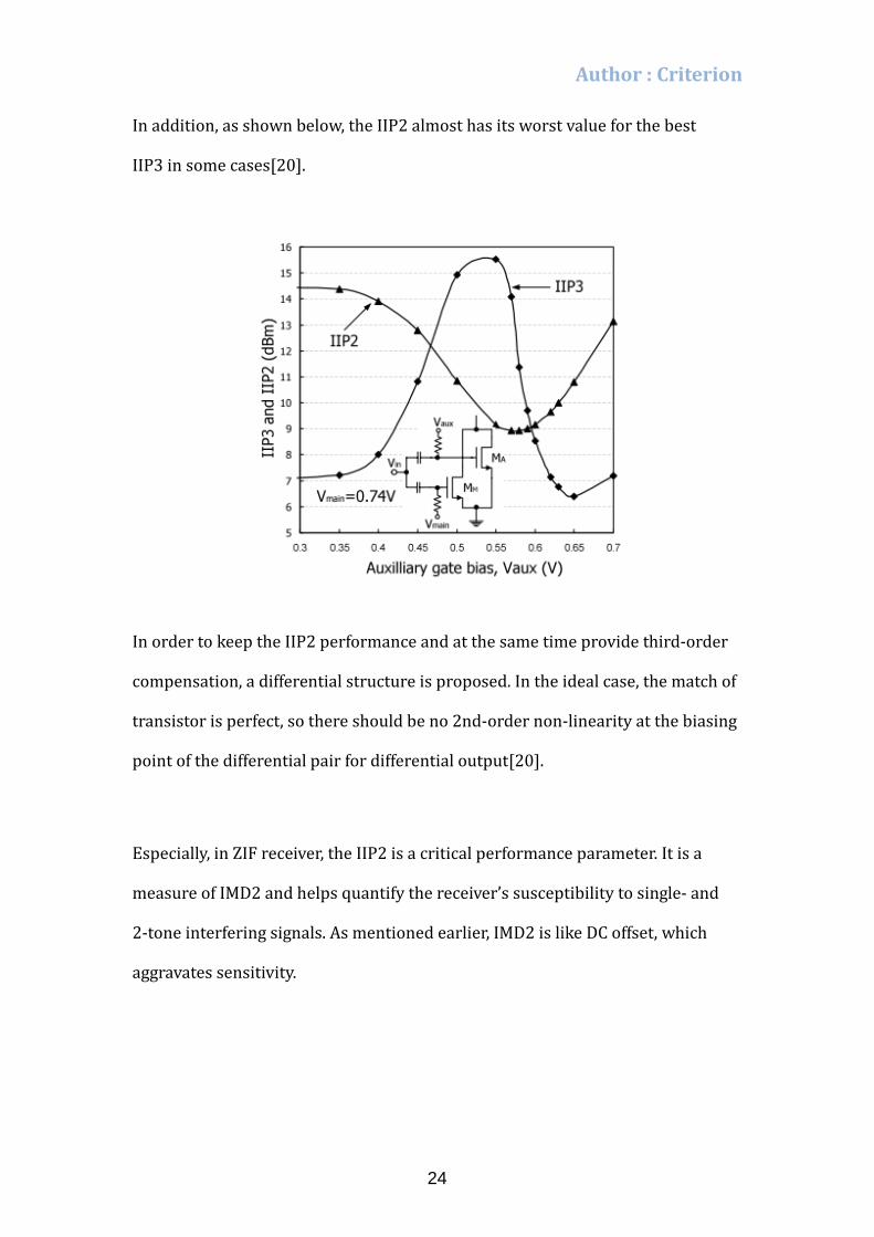
Author : Criterion
In addition, as shown below, the IIP2 almost has its worst value for the best
IIP3 in some cases[20].
In order to keep the IIP2 performance and at the same time provide third-order
compensation, a differential structure is proposed. In the ideal case, the match of
transistor is perfect, so there should be no 2nd-order non-linearity at the biasing
point of the differential pair for differential output[20].
Especially, in ZIF receiver, the IIP2 is a critical performance parameter. It is a
measure of IMD2 and helps quantify the receiver’s susceptibility to single- and
2-tone interfering signals. As mentioned earlier, IMD2 is like DC offset, which
aggravates sensitivity.
24
Author : Criterion
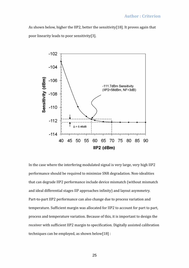
As shown below, higher the IIP2, better the sensitivity[18]. It proves again that
poor linearity leads to poor sensitivity[3].
In the case where the interfering modulated signal is very large, very high IIP2
performance should be required to minimize SNR degradation. Non-idealities
that can degrade IIP2 performance include device mismatch (without mismatch
and ideal differential stages IIP approaches infinity) and layout asymmetry.
Part-to-part IIP2 performance can also change due to process variation and
temperature. Sufficient margin was allocated for IIP2 to account for part to part,
process and temperature variation. Because of this, it is important to design the
receiver with sufficient IIP2 margin to specification. Digitally assisted calibration
techniques can be employed, as shown below[18] :
25

Author : Criterion
An automatic on chip IIP2 calibration routine is used to enhance IIP2 while also
accounting for interaction between the I and Q mixers[18]. Besides, large DC
offsets can degrade common-mode rejection ratio which can degrade IIP2 and
limit IIP2 calibration range. DC offsets generated from IIP2 calibration can limit
ADC headroom or require additional DC offset correction further down the
receiver chain. Changes in DC offset with IIP2 calibration are also undesirable
since a separate DC offset correction is required after each IIP2 calibration
adjustment. That’s the reason why an additional DC offset correction is built in
the circuit . The DC offset correction system is a critical component for ZIF
receiver design.
26
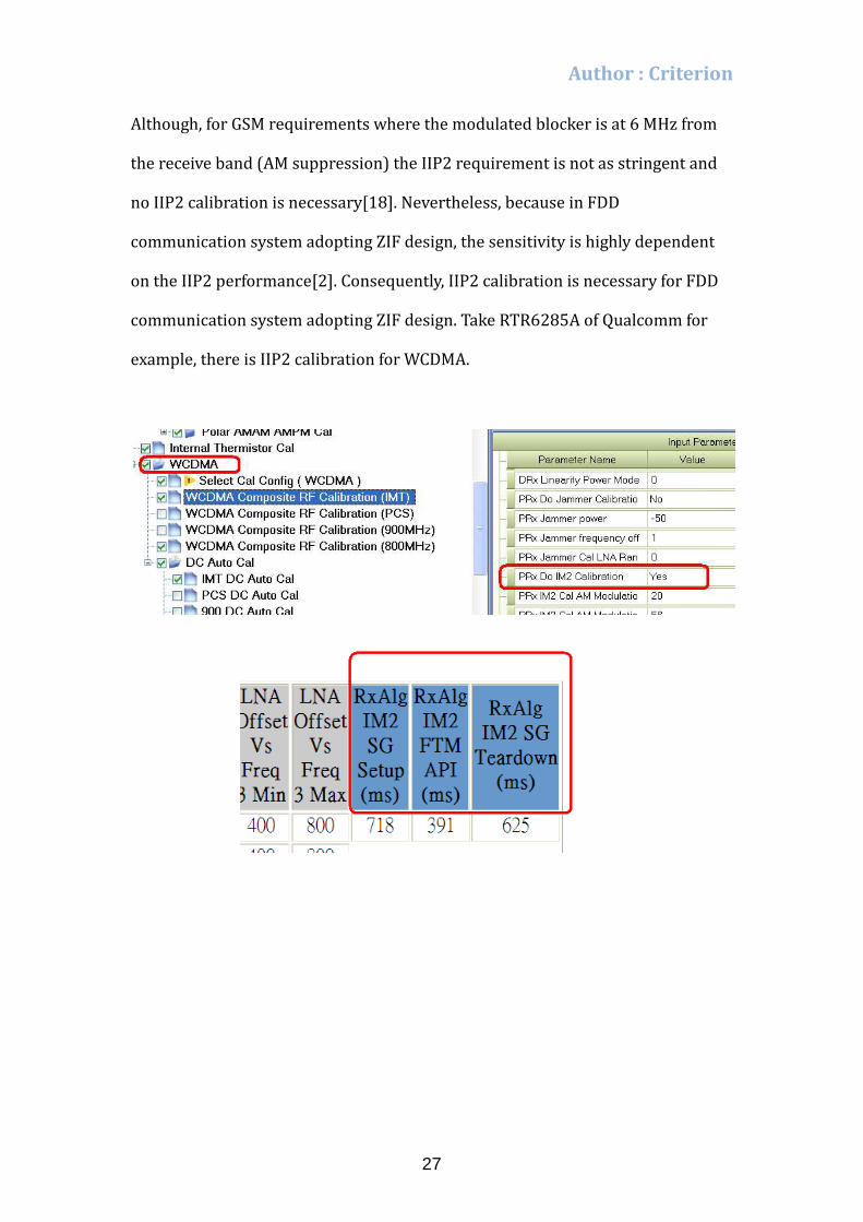
Author : Criterion
Although, for GSM requirements where the modulated blocker is at 6 MHz from
the receive band (AM suppression) the IIP2 requirement is not as stringent and
no IIP2 calibration is necessary[18]. Nevertheless, because in FDD
communication system adopting ZIF design, the sensitivity is highly dependent
on the IIP2 performance[2]. Consequently, IIP2 calibration is necessary for FDD
communication system adopting ZIF design. Take RTR6285A of Qualcomm for
example, there is IIP2 calibration for WCDMA.
27

Author : Criterion
Non-Ideal 90 degree balance in the I/Q demodulator produces unwanted images
which can be close to the carrier[11,27]. As shown above, the figure shows the
passband gain and stop-band rejection versus the I-Q phase and gain imbalance.
Any mismatch between the gain and phase of the two paths results in less
stop-band rejection and passband gain[6]. In ZIF, the signal along with the
blocker downconverts to baseband directly, and the sensitivity becomes
poor[6,27]. But an automatic on chip IIP2 calibration routine is used to enhance
IIP2 while accounting for interaction between the I and Q mixers[18].
28
Author : Criterion
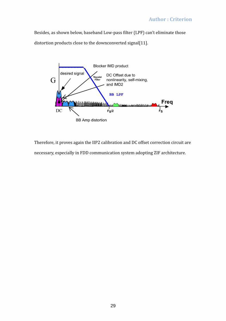
Besides, as shown below, baseband Low-pass filter (LPF) can’t eliminate those
distortion products close to the downconverted signal[11].
Therefore, it proves again the IIP2 calibration and DC offset correction circuit are
necessary, especially in FDD communication system adopting ZIF architecture.
29
Author : Criterion
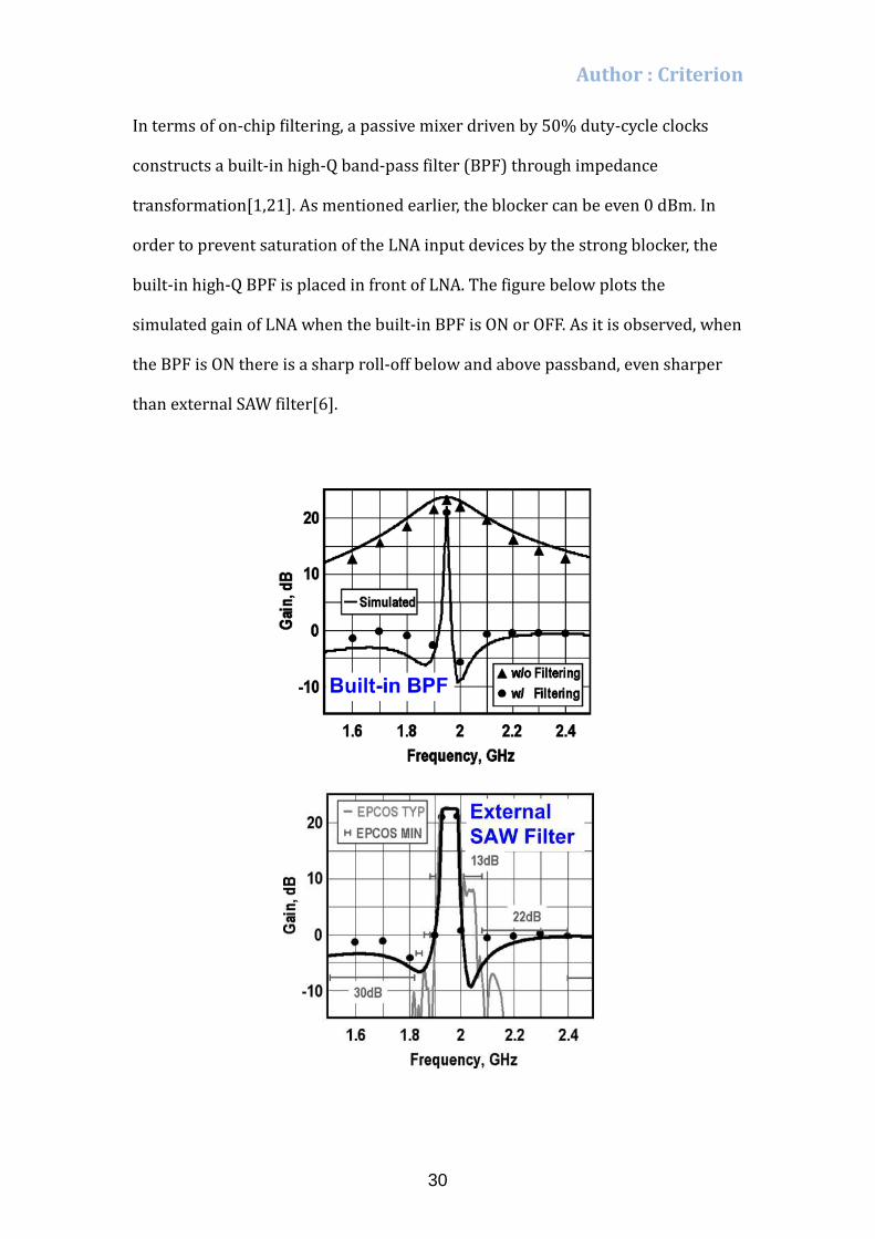
In terms of on-chip filtering, a passive mixer driven by 50% duty-cycle clocks
constructs a built-in high-Q band-pass filter (BPF) through impedance
transformation[1,21]. As mentioned earlier, the blocker can be even 0 dBm. In
order to prevent saturation of the LNA input devices by the strong blocker, the
built-in high-Q BPF is placed in front of LNA. The figure below plots the
simulated gain of LNA when the built-in BPF is ON or OFF. As it is observed, when
the BPF is ON there is a sharp roll-off below and above passband, even sharper
than external SAW filter[6].
30
Author : Criterion
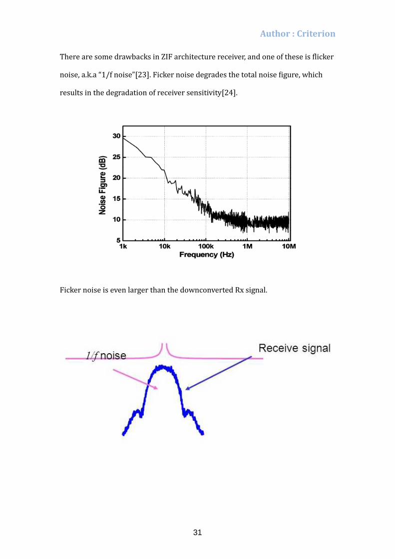
There are some drawbacks in ZIF architecture receiver, and one of these is flicker
noise, a.k.a “1/f noise”[23]. Ficker noise degrades the total noise figure, which
results in the degradation of receiver sensitivity[24].
Ficker noise is even larger than the downconverted Rx signal.
31
Author : Criterion
As mentioned in[3], the linearity of the mixer limits the whole linearity of the
receiver front-end and is effectively scaled down by the gain of LNA. Therefore, it
is essential to attain high linearity with low 1/f noise, which is difficult in active
mixers. Widely used active mixers suffer from high 1/f noise and poor linearity,
especially when the supply voltage is low. On the other hand, a current driven
passive mixer can provide relatively good linearity and inherent low 1/f noise
performance due to the absence of DC current[22]. Thus, in general, passive
CMOS mixers are considered as the appropriate choice for ZIF receivers because
they do not contribute to 1/f noise [24]. Furthermore, the passive mixer is
chosen not only for its well-known better 1/f noise and linearity over the active
mixer in low supply voltage applications, but also for its impedance
transformation property, which has been widely utilized to construct a built-in
high-Q BPF suppressing the transmitter leakage and other blockers[21].
32
Author : Criterion
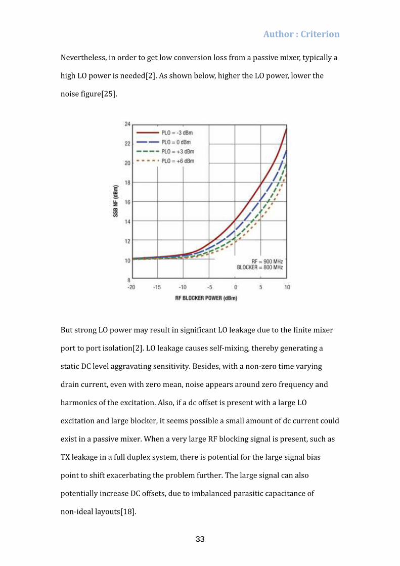
Nevertheless, in order to get low conversion loss from a passive mixer, typically a
high LO power is needed[2]. As shown below, higher the LO power, lower the
noise figure[25].
But strong LO power may result in significant LO leakage due to the finite mixer
port to port isolation[2]. LO leakage causes self-mixing, thereby generating a
static DC level aggravating sensitivity. Besides, with a non-zero time varying
drain current, even with zero mean, noise appears around zero frequency and
harmonics of the excitation. Also, if a dc offset is present with a large LO
excitation and large blocker, it seems possible a small amount of dc current could
exist in a passive mixer. When a very large RF blocking signal is present, such as
TX leakage in a full duplex system, there is potential for the large signal bias
point to shift exacerbating the problem further. The large signal can also
potentially increase DC offsets, due to imbalanced parasitic capacitance of
non-ideal layouts[18].
33
Author : Criterion
It has been demonstrated that increasing AC current through a mixer device
channel with a large RF blocker can generate considerably more 1/f noise and
DC offset. This is a significant concern for SAW-less operation. In conventional
ZIF receiver architectures, with 50% duty-cycle LO waveforms generation, the
mixer devices are either on or off. However with non-ideal rise and fall times, it
causes the total noise referred to the output of the baseband amplifier to
increase. However, compared to 50% duty-cycle, the DC induced currents are
lower with 25% duty-cycle LO. And the 1/f noise will have less contribution to
overall noise after commutation for a 25% duty-cycle system, resulting in less
noise amplification at baseband and larger signal to noise(SNR). 25% duty-cycle
LO waveforms result in improved 1/f noise and DC offset performance even
though with large blocking signals as well[18].
34
Author : Criterion
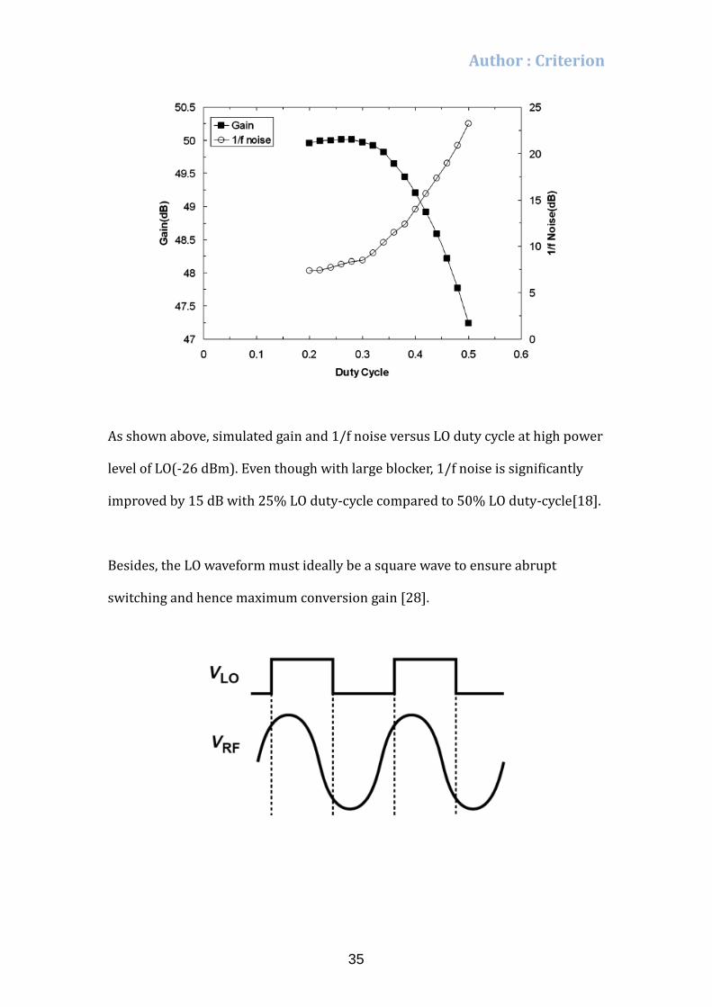
As shown above, simulated gain and 1/f noise versus LO duty cycle at high power
level of LO(-26 dBm). Even though with large blocker, 1/f noise is significantly
improved by 15 dB with 25% LO duty-cycle compared to 50% LO duty-cycle[18].
Besides, the LO waveform must ideally be a square wave to ensure abrupt
switching and hence maximum conversion gain [28].
35
Author : Criterion
Thus, in a ZIF receiver where the passive I and Q mixer are clocked with a 25%
duty-cycle LO, resulting in higher receiver gain relative to a 50% duty-cycle
implementation, a 3 dB improvement in gain by using 25% duty-cycle, as shown
above[18,28]. Besides, as mentioned earlier, I/Q imbalance results in image issue,
aggravating sensitivity. But with the 25% duty-cycle mixer design, the image
problem is eliminated[17,21]. On the other hand, as mentioned earlier, the IIP2
almost has its worst value for the best IIP3 in some cases. But a significant
advantage of using a passive mixer with 25% duty-cycle is that it is not sensitive
to increased IMD distortion when a large blocker is present. The results show
that the receiver IIP3 performance is improved significantly with 25% duty-cycle
compared to 50% duty-cycle. That is to say, with the 25% duty-cycle LO injection
into a passive mixer, which results in 3 dB additional gain; as well as lower noise
figure, IMD distortion and 1/f noise. Of course, with IIP2 calibration, these
improve more[18].
Consequently, if passive I and Q mixer are clocked with a 25% duty-cycle LO,
there are some advantages, as summaried below :
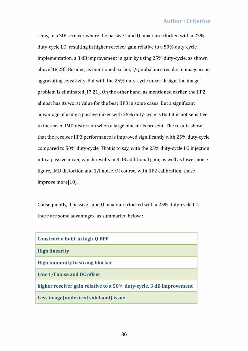
Construct a built-in high-Q BPF
High linearity
High immunity to strong blocker
Low 1/f noise and DC offset
higher receiver gain relative to a 50% duty-cycle, 3 dB improvement
Less image(undesired sideband) issue
36

Author : Criterion
As for duplexer, in addition to selecting a high isolation duplexer, the layout is
also critical. As shown below, we need to enhance isolation by means of good
layout.
We take SAYRF1G95HQ0F0A of Murata for example, because Tx port is far away
from Rx port. That is to say, there is good isolation between the layout traces
from the two ports.
37
Author : Criterion
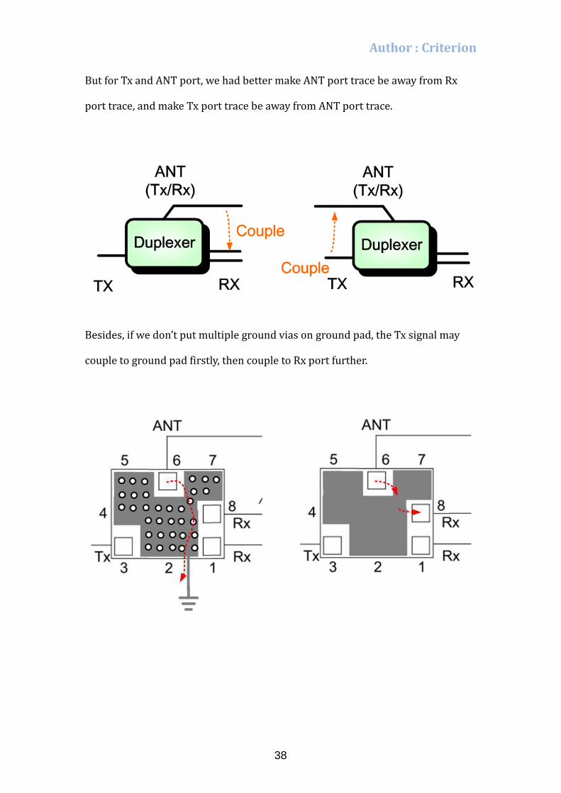
But for Tx and ANT port, we had better make ANT port trace be away from Rx
port trace, and make Tx port trace be away from ANT port trace.
Besides, if we don’t put multiple ground vias on ground pad, the Tx signal may
couple to ground pad firstly, then couple to Rx port further.
38

Author : Criterion
Consequently, as shown below, the correct PCB layout for duplexer should be like
this.
39
Author : Criterion
Reference
[1] A 65 nm CMOS Quad-Band SAW-Less Receiver SoC for GSM/GPRS/EDGE,
IEEE
[2] CDMA Zero-IF Receiver Consideration, Slideshare
[3] Sensitivity or selectivity -- How does eLNA impact the receriver performance,
Slideshare
[4] System(Board level) Noise Figure analysis and optimization,Slideshare
[5] On the Direct Conversion Receiver -- A Tutorial
[6] A Blocker Filtering Technique for SAW-Less Wireless Receivers
[7] A Blocker-Tolerant, Noise-Cancelling Receiver Suitable for Wideband
Wireless Applications
[8] Multi-Mode Multi-Band RF Transceivers for Wireless Communications
[9] ALM-1106 GPS Low Noise amplifier with Variable bias current and Shutdown
function, AVAGO
[10] Performance of spread spectrum system
[11] Wireless Technologies: Circuits, Systems, and Devices
[12] An Integrated GSM/DECT Receiver: Design Specifications
[13] Interference Mitigation Techniques for SAW-less CDMA Receivers
[14] HHM17147A1 for 673~2700MHz, MULTILAYER BALUN SPECIFICATION ,
TDK
[15] How to solve ACLR issue, Slideshare
[16] Design of a Direct Conversion Transmitter to Resist Combined Effects of
Power Amplifier Distortion and Local Oscillator Pulling
[17] Wireless Transceiver Circuits System Perspectives and Design Aspects
40

Author : Criterion
[18] A Single–Chip 10-Band WCDMA/HSDPA 4-Band GSM/EDGE SAW-less CMOS
Receiver With DigRF 3G Interface and +90 dBm IIP2
[19] A Comparative Study of Linearization Techniques of CMOS LNA
[20] A LINEARIZATION TECHNIQUE FOR RF LOW NOISE AMPLIFIER
[21] Analysis and design of a high-linearity receiver RF front-end with an
improved 25%-duty-cycle LO generator for WCDMA/GSM applications
[22] Image-Reject Mixer Arms Direct-Conversion Receivers
[23] Study of Flicker Noise for Zero-IF Receiver
[24] Design and Analysis of Low Flicker-Noise CMOS Mixers for
Direct-Conversion Receivers
[25] Passive Mixers in Downconverter Applications
[26] Understanding IP2 and IP3 Issues in Direct Conversion Receivers for
WCDMA Wide Area Basestations
[27] Introduction to I/Q signal, Slideshare
[28] RF MICROELECTRONICS—Mixer
41